an2839 application note - stmicroelectronics › resource › en › application_note › cd... ·...
TRANSCRIPT
September 2009 Doc ID 15104 Rev 1 1/40
AN2839Application note
L6228 fully-integrated two-phase stepper motor driver
IntroductionModern motion control applications need more flexibility, which can only be addressed with specialized IC products. The L6228 is a fully-integrated stepper motor driver IC specifically developed to drive a wide range of two-phase (bipolar) stepper motors. This IC is a one-chip, cost-effective solution that includes several unique circuit design features. These features, including a decoding logic that can generate three different stepping sequences, allow the device to be used in many applications, including microstepping. The principal aim of this development project was to produce an easy-to-use, fully-protected power IC. In addition, several key functions, such as protection circuitry and PWM current control, drastically reduce the number of external components to meet requirements for many different applications.
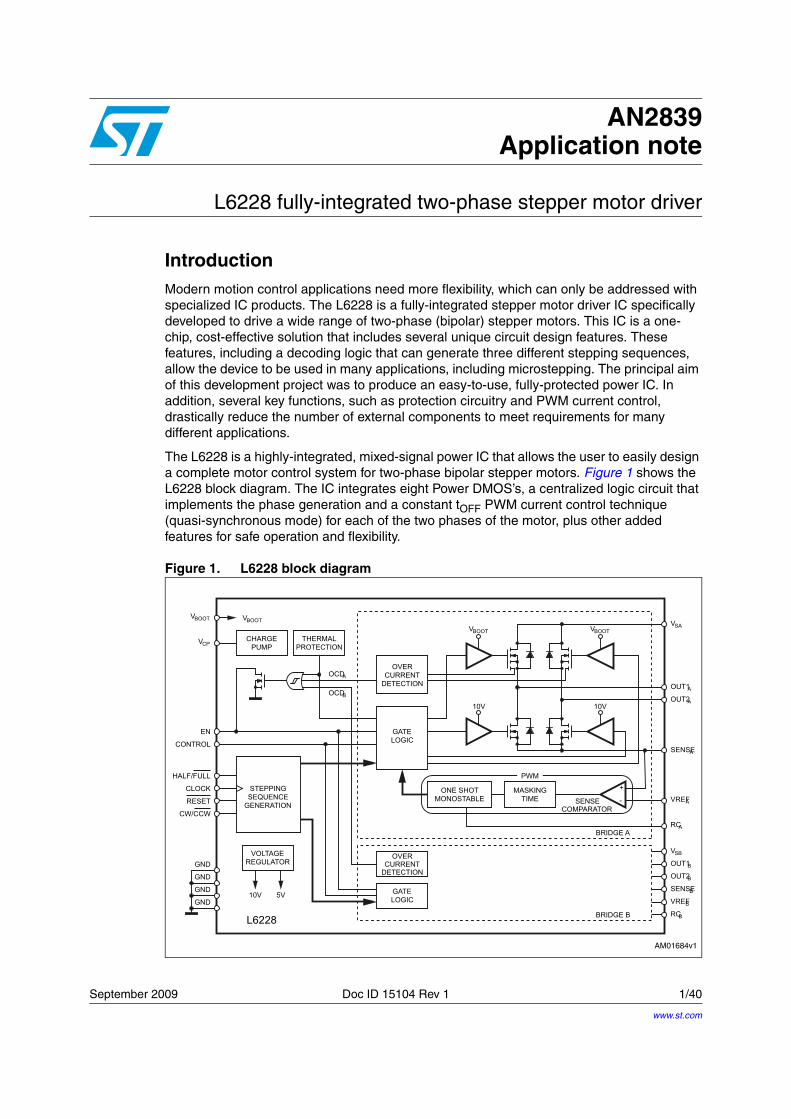
The L6228 is a highly-integrated, mixed-signal power IC that allows the user to easily design a complete motor control system for two-phase bipolar stepper motors. Figure 1 shows the L6228 block diagram. The IC integrates eight Power DMOS’s, a centralized logic circuit that implements the phase generation and a constant tOFF PWM current control technique (quasi-synchronous mode) for each of the two phases of the motor, plus other added features for safe operation and flexibility.
Figure 1. L6228 block diagram
www.st.com

Contents AN2839
2/40 Doc ID 15104 Rev 1
Contents
1 Designing an application with L6228 . . . . . . . . . . . . . . . . . . . . . . . . . . . 4
1.1 Current ratings . . . . . . . . . . . . . . . . . . . . . . . . . . . . . . . . . . . . . . . . . . . . . . 4
1.2 Voltage ratings and operating range . . . . . . . . . . . . . . . . . . . . . . . . . . . . . . 4
1.3 Choosing the bulk capacitor . . . . . . . . . . . . . . . . . . . . . . . . . . . . . . . . . . . . 6
1.4 Layout considerations . . . . . . . . . . . . . . . . . . . . . . . . . . . . . . . . . . . . . . . . . 7
1.5 Sensing resistors . . . . . . . . . . . . . . . . . . . . . . . . . . . . . . . . . . . . . . . . . . . . 9
1.6 External components for the charge pump . . . . . . . . . . . . . . . . . . . . . . . 10
1.7 Sharing the charge pump circuitry . . . . . . . . . . . . . . . . . . . . . . . . . . . . . . 11
1.8 Reference voltage for PWM current control . . . . . . . . . . . . . . . . . . . . . . . 12
1.9 Input logic pins . . . . . . . . . . . . . . . . . . . . . . . . . . . . . . . . . . . . . . . . . . . . . 13
1.10 EN pin . . . . . . . . . . . . . . . . . . . . . . . . . . . . . . . . . . . . . . . . . . . . . . . . . . . 13
1.11 Programmable off time monostable . . . . . . . . . . . . . . . . . . . . . . . . . . . . . 14
1.11.1 Off time selection and minimum on time . . . . . . . . . . . . . . . . . . . . . . . . 16
1.11.2 Decay modes . . . . . . . . . . . . . . . . . . . . . . . . . . . . . . . . . . . . . . . . . . . . . 16
1.12 Overcurrent protection . . . . . . . . . . . . . . . . . . . . . . . . . . . . . . . . . . . . . . . 18
1.13 Power management . . . . . . . . . . . . . . . . . . . . . . . . . . . . . . . . . . . . . . . . . 21
1.13.1 Maximum output current versus selectable devices . . . . . . . . . . . . . . . 23
1.13.2 Power dissipation and thermal analysis with PractiSPINTM software . . 23
1.14 Choosing the decay mode . . . . . . . . . . . . . . . . . . . . . . . . . . . . . . . . . . . . 24
1.15 Choosing the stepping sequence . . . . . . . . . . . . . . . . . . . . . . . . . . . . . . . 25
1.16 Microstepping . . . . . . . . . . . . . . . . . . . . . . . . . . . . . . . . . . . . . . . . . . . . . . 27
2 Application example . . . . . . . . . . . . . . . . . . . . . . . . . . . . . . . . . . . . . . . . 29
Appendix A Demonstration board. . . . . . . . . . . . . . . . . . . . . . . . . . . . . . . . . . . . . 31
A.1 PractiSPINTM . . . . . . . . . . . . . . . . . . . . . . . . . . . . . . . . . . . . . . . . . . . . . . . 31
A.2 L6228N evaluation with EVAL6208N. . . . . . . . . . . . . . . . . . . . . . . . . . . . . 32
A.2.1 Important notes. . . . . . . . . . . . . . . . . . . . . . . . . . . . . . . . . . . . . . . . . . . . 32
A.3 EVAL6228QR . . . . . . . . . . . . . . . . . . . . . . . . . . . . . . . . . . . . . . . . . . . . . . 34
References. . . . . . . . . . . . . . . . . . . . . . . . . . . . . . . . . . . . . . . . . . . . . . . . . . . . . . . . . 38
Revision history . . . . . . . . . . . . . . . . . . . . . . . . . . . . . . . . . . . . . . . . . . . . . . . . . . . . 39

AN2839 List of figures
Doc ID 15104 Rev 1 3/40
List of figures
Figure 1. L6228 block diagram . . . . . . . . . . . . . . . . . . . . . . . . . . . . . . . . . . . . . . . . . . . . . . . . . . . . . . 1Figure 2. Supply voltage of high-side gate drivers versus supply voltage . . . . . . . . . . . . . . . . . . . . . . 4Figure 3. Currents and voltages during the dead time at the beginning of the off time . . . . . . . . . . . . 5Figure 4. Voltage at the two outputs at the beginning of the off-time. . . . . . . . . . . . . . . . . . . . . . . . . . 6Figure 5. Typical application and layout suggestions . . . . . . . . . . . . . . . . . . . . . . . . . . . . . . . . . . . . . 8Figure 6. Two situations that must be avoided . . . . . . . . . . . . . . . . . . . . . . . . . . . . . . . . . . . . . . . . . . 9Figure 7. Charge pump . . . . . . . . . . . . . . . . . . . . . . . . . . . . . . . . . . . . . . . . . . . . . . . . . . . . . . . . . . . 10Figure 8. Sharing the charge-pump circuitry . . . . . . . . . . . . . . . . . . . . . . . . . . . . . . . . . . . . . . . . . . . 11Figure 9. Obtaining a variable voltage through a PWM output of a µC . . . . . . . . . . . . . . . . . . . . . . 12Figure 10. Logic input pins. . . . . . . . . . . . . . . . . . . . . . . . . . . . . . . . . . . . . . . . . . . . . . . . . . . . . . . . . . 13Figure 11. EN input pin . . . . . . . . . . . . . . . . . . . . . . . . . . . . . . . . . . . . . . . . . . . . . . . . . . . . . . . . . . . . 13Figure 12. Simplified schematic of the PWM current controller . . . . . . . . . . . . . . . . . . . . . . . . . . . . . . 14Figure 13. Output current regulation waveforms . . . . . . . . . . . . . . . . . . . . . . . . . . . . . . . . . . . . . . . . . 15Figure 14. Typical off time vs. COFF for several values of ROFF . . . . . . . . . . . . . . . . . . . . . . . . . . . . . 16Figure 15. Minimum on time vs. COFF . . . . . . . . . . . . . . . . . . . . . . . . . . . . . . . . . . . . . . . . . . . . . . . . . 16Figure 16. Fast decay mode output stage configurations . . . . . . . . . . . . . . . . . . . . . . . . . . . . . . . . . . 17Figure 17. Slow decay mode output stage configurations . . . . . . . . . . . . . . . . . . . . . . . . . . . . . . . . . . 17Figure 18. PWM controller loses the current regulation due to minimum on time . . . . . . . . . . . . . . . . 18Figure 19. PWM controller loses the current regulation due to minimum on time - detail . . . . . . . . . . 18Figure 20. Simplified circuitry of the overcurrent detection . . . . . . . . . . . . . . . . . . . . . . . . . . . . . . . . . 19Figure 21. Overcurrent operation: timing 1 . . . . . . . . . . . . . . . . . . . . . . . . . . . . . . . . . . . . . . . . . . . . . 20Figure 22. Overcurrent operation: timing 2 . . . . . . . . . . . . . . . . . . . . . . . . . . . . . . . . . . . . . . . . . . . . . 20Figure 23. Typical disable time vs. CEN for several values of REN . . . . . . . . . . . . . . . . . . . . . . . . . . . 21Figure 24. Typical delay time vs. CEN . . . . . . . . . . . . . . . . . . . . . . . . . . . . . . . . . . . . . . . . . . . . . . . . . 21Figure 25. IC dissipated power versus output current . . . . . . . . . . . . . . . . . . . . . . . . . . . . . . . . . . . . . 22Figure 26. Maximum output current vs. selectable devices . . . . . . . . . . . . . . . . . . . . . . . . . . . . . . . . . 23Figure 27. Power dissipation and thermal analysis with PractiSPINTM software . . . . . . . . . . . . . . . . . 24Figure 28. Torque instability in full-step mode. . . . . . . . . . . . . . . . . . . . . . . . . . . . . . . . . . . . . . . . . . . 25Figure 29. Balanced half step for low torque ripple . . . . . . . . . . . . . . . . . . . . . . . . . . . . . . . . . . . . . . . 26Figure 30. Realizing half-step current shaping . . . . . . . . . . . . . . . . . . . . . . . . . . . . . . . . . . . . . . . . . . 26Figure 31. Microstepping application . . . . . . . . . . . . . . . . . . . . . . . . . . . . . . . . . . . . . . . . . . . . . . . . . . 27Figure 32. Microstepping reference voltages, output currents and CLOCK signal . . . . . . . . . . . . . . 27Figure 33. Using fast decay during a high, negative current slope . . . . . . . . . . . . . . . . . . . . . . . . . . . 28Figure 34. Application example . . . . . . . . . . . . . . . . . . . . . . . . . . . . . . . . . . . . . . . . . . . . . . . . . . . . . . 30Figure 35. PractiSPINTM PC software . . . . . . . . . . . . . . . . . . . . . . . . . . . . . . . . . . . . . . . . . . . . . . . . . 31Figure 36. PractiSPINTM ST7 demonstration board. . . . . . . . . . . . . . . . . . . . . . . . . . . . . . . . . . . . . . . 32Figure 37. EVAL6208N electrical schematic . . . . . . . . . . . . . . . . . . . . . . . . . . . . . . . . . . . . . . . . . . . . 33Figure 38. EVAL6228QR . . . . . . . . . . . . . . . . . . . . . . . . . . . . . . . . . . . . . . . . . . . . . . . . . . . . . . . . . . . 34Figure 39. EVAL6228QR component placement . . . . . . . . . . . . . . . . . . . . . . . . . . . . . . . . . . . . . . . . . 35Figure 40. EVAL6228QR top layer . . . . . . . . . . . . . . . . . . . . . . . . . . . . . . . . . . . . . . . . . . . . . . . . . . . 36Figure 41. EVAL6228QR bottom layer . . . . . . . . . . . . . . . . . . . . . . . . . . . . . . . . . . . . . . . . . . . . . . . . 36Figure 42. EVAL6228QR electrical schematic . . . . . . . . . . . . . . . . . . . . . . . . . . . . . . . . . . . . . . . . . . . 37

Designing an application with L6228 AN2839
4/40 Doc ID 15104 Rev 1
1 Designing an application with L6228
1.1 Current ratingsWith MOSFET (DMOS) devices, unlike bipolar transistors, the current under short-circuit conditions is, at a first approximation, limited by the RDS(on) of the DMOS themselves and can reach very high values. The L6228’s OUT pins and the two VSA and VSB pins are rated for a maximum of 1.4 Arms and 2.8 A peak (typical values), corresponding to a total of 2.8 Arms (5.6 A peak) for the whole IC. These values are meant to avoid damaging the metal structures, including the metallization on the die and bond wires. In practical applications, however, the maximum-allowable current is less than these values, due to power dissipation limits (see Section 1.13). The device has a built-in overcurrent detection (OCD) that provides protection against short-circuits between the outputs and between an output and ground (see Section 1.12).
1.2 Voltage ratings and operating rangeThe L6228 requires a single supply voltage (VS) for the motor supply. Internal voltage regulators provide the 5 and 10 volts required for the internal circuitry. The operating range for VS is 8 to 52 V. To prevent the device from operating at an insufficient supply voltage, an undervoltage lockout (UVLO) circuit shuts down the device when the supply voltage falls below 5.5 V; to resume normal operating conditions, VS must then exceed 6.3 V. The hysteresis is provided to avoid false intervention of the UVLO function during fast VS ringings. It should be noted, however, that the DMOS' RDS(on) is a function of the VS supply voltage. In fact, when VS is less than 10 V, RDS(on) is adversely affected, and this is particularly true for the high-side DMOS’s that are driven from the VBOOT supply. This supply is obtained through a charge pump from the internal 10 V supply, which will tend to reduce its output voltage when VS goes below 10 V. Figure 2 shows the supply voltage of the high-side gate drivers (VBOOT - VS) versus the supply voltage (VS).
Figure 2. Supply voltage of high-side gate drivers versus supply voltage
Note that VS must be connected to both VSA and VSB since the bootstrap voltage (at the VBOOT pin) is the same for the two H-bridges. The integrated DMOS’s have a rated drain-source breakdown voltage of 60 V. However, VS should be kept below 52 V, since in normal working conditions the DMOS’s see a Vds voltage that will exceed the VS supply. In particular, when using the fast-decay mode, at the beginning of the off time (when all the DMOS’s are off during dead time) the SENSE pin sees a negative spike due to a non-negligible parasitic inductance of the PCB path from the pin to GND.

AN2839 Designing an application with L6228
Doc ID 15104 Rev 1 5/40
This spike is followed by a stable negative voltage due to the drop on RSENSE. One of the two OUT pins of the bridge sees a similar behavior, but with a slightly larger voltage due to the forward recovery time of the integrated freewheeling diode and the forward voltage drop across it (see Figure 3). The typical duration of this spike is 30 ns. At the same time, the other OUT pin of the same bridge sees a voltage above VS, due to the PCB inductance and voltage drop across the high-side (integrated) freewheeling diode, as the current reverses direction and flows into the bulk capacitor. It turns out that, in fast decay mode, the highest differential voltage is observed between the two OUT pins of the same bridge, at the beginning of the off time, and this must always be kept below 60 V(a). The same high-voltage condition exists when a step is made and the direction of the current flow reverses in the bridge.
Figure 3. Currents and voltages during the dead time at the beginning of the off time
Figure 4 on page 6 shows the voltage waveforms at the two OUT pins referring to a possible practical situation, with a peak output current of 1.4 A, VS = 52 V, RSENSE = 0.33 Ω, TJ = 25 °C (approximately) and a good PCB layout. The below-ground spike amplitude is -2.65 V for one output; the other OUT pin is at about 57 V. In these conditions, the total differential voltage reaches almost 60 V, which is the absolute maximum rating for the DMOS. It is extremely important to keep the differential voltage between two output pins belonging to the same full bridge within rated values. This can be accomplished by correctly selecting the value of the bulk capacitor and equivalent series resistance (ESR), according to the current peaks and chopping style, and by adopting good layout practices to minimize PCB parasitic inductances(a).
a. Refer to [3] in References.

Designing an application with L6228 AN2839
6/40 Doc ID 15104 Rev 1
Figure 4. Voltage at the two outputs at the beginning of the off-time
1.3 Choosing the bulk capacitorSince the bulk capacitor, placed between the VS and GND pins, is charged and discharged during IC operation, its AC current capability must be greater than the RMS value of the charge/discharge current. This current flows from the capacitor to the IC during the on time (tON) and from the IC (in fast decay; from the power supply in slow decay) to the capacitor during the off time (tOFF). The RMS value of the current flowing into the bulk capacitor depends on the peak output current, output current ripple, switching frequency, duty cycle and chopping style. It also depends on the characteristics of the power supply. A power supply with poor high-frequency performances (or long, inductive connections to the IC) will cause the bulk capacitor to be recharged slowly: the higher the current control switching frequency, the higher the current ripple in the capacitor; RMS current in the capacitor, however, does not exceed the RMS output current. The bulk capacitor value (C) and the ESR determine the amount of voltage ripple on the capacitor itself and on the IC. In slow decay, neglecting the dead-time and output current ripple, and assuming that during the on time the capacitor is not recharged by the power supply, the voltage at the end of the on time is:
Equation 1
so the supply voltage ripple is:
Equation 2
where IOUT is the output current. In fast decay, instead, the recirculating current recharges the capacitor, causing the supply voltage to exceed the nominal voltage. This can be very dangerous if the nominal supply voltage is close to the maximum recommended supply voltage (52 V).
In fast decay the supply voltage ripple is about:
VS IOUT– ESRtON
C-----------+⎝ ⎠
⎛ ⎞⋅
IOUT ESRtON
C-----------+⎝ ⎠
⎛ ⎞⋅

AN2839 Designing an application with L6228
Doc ID 15104 Rev 1 7/40
Equation 3
always assuming that the power supply does not recharge the capacitor, and neglecting the output current ripple and the dead-time. Usually (if C > 100 µF) the capacitance role is much less than the ESR, in which case the supply voltage ripple can be estimated as:
Equation 4
Equation 5
For example, if a maximum ripple of 500 mV is allowed and IOUT = 1 A, the capacitor ESR should be lower than:
Equation 6
Equation 7
In fact, current sunk by the VSA and VSB pins of the device is subject to higher peaks due to the reverse recovery charge of the internal freewheeling diodes. The duration of these peaks is very short and can be filtered using a small value (100÷200 nF), good-quality ceramic capacitor connected as close as possible to the VSA, VSB and GND pins of the IC. The bulk capacitor should be chosen with a maximum operating voltage 25% greater than the maximum supply voltage, considering also the power supply tolerances. For example, with a 48 V nominal power supply with 5% tolerance, the maximum voltage will be 50.4 V, and the operating voltage for the capacitor should be at least 63 V.
1.4 Layout considerationsWorking with devices that combine high-power switches and control logic in the same IC, special attention has to be paid to the layout of the PCB. In extreme cases, Power DMOS commutation can induce noise that may cause improper operation in the logic section of the device. Noise can be radiated by high dV/dt nodes or high dI/dt paths, or conducted through GND or supply connections. Logic connections, especially high-impedance nodes (actually all logic inputs, see Section 1.9), must be kept far from switching nodes and paths. With the L6228 in particular, the external components for the charge-pump circuitry should be connected together through short paths, since these components are subject to voltage and current switching at a relatively high frequency (600 kHz). The primary means of minimizing conducted noise is to work on a good GND layout (see Figure 5 on page 8).
IOUT 2 ESR⋅tON tOFF+
C--------------------------------+⎝ ⎠
⎛ ⎞⋅
IOUT ESR⋅
2 IOUT ESR⋅ ⋅
ESR 0.5V1A
------------< 500mΩ= in slow decay
in fast decayESR12--- 0.5V
1A------------⋅< 250mΩ=

Designing an application with L6228 AN2839
8/40 Doc ID 15104 Rev 1
Figure 5. Typical application and layout suggestions
The high current GND tracks (the tracks connected to the sensing resistors) must be connected directly to the negative terminal of the bulk capacitor. A good quality, high-frequency bypass capacitor is also required (typically a 100÷200 nF ceramic would suffice), since electrolytic capacitors show a poor high-frequency performance. Both bulk electrolytic and high-frequency bypass capacitors have to be connected with short tracks to VSA, VSB and GND. On the L6228 the GND pins are the logic GND since only the quiescent current flows through them. The logic GND and power GND should be connected together in a single point, the bulk capacitor, to keep noise in the power GND from affecting the logic GND. Specific care should be paid layouting the path from the SENSE pins through the sensing resistors to the negative terminal of the bulk capacitor (power ground). These tracks must be as short as possible to minimize parasitic inductances that can cause dangerous voltage spikes on the SENSE and OUT pins (see Section 1.2); for the same reason the capacitors on VSA, VSB and GND should be very close to the GND and supply pins. Refer to Section 1.5 for information on selecting the sense resistors. The traces connected to VSA, VSB, SENSEA, SENSEB, and the four OUT pins must be designed with adequate width, since high currents flow through these traces, and layer changes should be avoided. Should a layer change prove necessary, multiple and large via holes have to be used. A wide GND copper area can be used to improve heat removal, thus reducing thermal resistance.
Figure 6 on page 9 shows two typical situations that must be avoided. An important consideration regarding the location of the bulk capacitors is the ability to absorb the inductive energy from the load, without allowing the supply voltage to exceed the maximum rating. The diode shown in Figure 6 prevents the recirculation current from reaching the capacitors and will result in a high voltage on the IC pins that can damage the device. Having a switch or a power connection that can disconnect the capacitors from the IC, while there is still current in the motor, will also result in a high voltage transient since there is no capacitance to sink the recirculating current.

AN2839 Designing an application with L6228
Doc ID 15104 Rev 1 9/40
Figure 6. Two situations that must be avoided
1.5 Sensing resistorsEach motor winding current flows through the corresponding sensing resistor, causing a voltage drop that is used, by the logic, to control the peak value of the load current. Two important points must be taken into account when choosing the RSENSE value.
● The sensing resistor dissipates energy and provides dangerous negative voltages on the SENSE pin during the current recirculation. For this reason, the resistance of this component should be kept low.
● The voltage drop across RSENSE is compared with the reference voltage (on the Vref pin) by the internal comparator. The lower the RSENSE value, the higher the peak current error due to noise on the Vref pin and to the input offset of the current sense comparator: RSENSE values that are too small must be avoided.
A good compromise is to calculate the sensing resistor value so that the voltage drop, corresponding to the peak current in the load (Ipeak), is about 0.5 V: RSENSE = 0.5 V/Ipeak.
The sensing resistor must be of a non-inductive type in order to avoid dangerous negative spikes on the SENSE pins. Wire-wound resistors cannot be used here, while metallic film resistors are recommended for their high peak current capability and low inductance. For the same reason, the connections between the SENSE pins, C6, C7, VSA, VSB and GND pins (see Figure 5 on page 8) must be as short as possible (also see Section 1.4).
The average power dissipated by the sensing resistor is:
● Fast decay recirculation: PR ≈ Irms2 · RSENSE
● Slow decay recirculation: PR ≈ Irms2 · RSENSE · D
where D is the duty-cycle of the PWM current control and Irms is the RMS value of the load current. Nevertheless, the peak value of the dissipated power should be taken into account when choosing the power rating of the sensing resistor.
Equation 8
PR Ipk2
RSENSE⋅≈

Designing an application with L6228 AN2839
10/40 Doc ID 15104 Rev 1
where Ipk is the peak value of the load current.
Using multiple resistors in parallel will help obtain the required power rating with standard resistors and reduce the inductance.
The RSENSE tolerance reflects on the peak current error: 1% resistors should be preferred. Table 1 shows the recommended values for RSENSE (to obtain a 0.5-V drop) and power ratings for typical examples of current peak values.
1.6 External components for the charge pumpAn internal oscillator, with its output at the CP pin, switches from GND to 10 V with a typical frequency of 600 kHz (Figure 7).
Figure 7. Charge pump
When the oscillator output is at ground, C5 is charged by VS through D2. When it rises to 10 V, D2 is reverse-biased and the charge flows from C5 to C8 through D1, so the VBOOT pin, after a few cycles, reaches the maximum voltage of VS + 10 V - VD1 - VD2, which supplies the high-side gate drivers.
With a differential voltage between VS and VBOOT of about 9 V and both bridges switching at 50 kHz, the typical current drawn by the VBOOT pin is 1.85 mA.
Table 1. RSENSE recommended values
Ipk RSENSE value [Ω] RSENSE power rating [W] Alternatives
0.25 2 0.125
0.5 1 0.25
1 0.5 0.5 2 X 1 Ω, 0.25 W paralleled

AN2839 Designing an application with L6228
Doc ID 15104 Rev 1 11/40
To minimize interferences with the rest of the circuit, care must be taken in realizing the PCB layout of the C5, D1 and D2 connections (also see Section 1.4). The recommended values for the charge pump circuitry are:
● D1, D2: 1N4148
● C5: 10 nF, 100 V ceramic
● C8: 20 nF, 25 V ceramic
Due to the high charge-pump frequency, fast diodes are required. When connecting the cold side of the bulk capacitor (C8) to VS instead of GND, the average current in the external diodes during operation is less than 10 mA; at startup (when VS is provided to the IC) it is less than 200 mA while the reverse voltage is about 10 V in all conditions. IN4148 diodes withstand about 200 mA of DC current (1 A peak), and the maximum reverse voltage is 75 V, so they should fit for the majority of applications.
1.7 Sharing the charge pump circuitryIf more than one device is used in the application, the charge pump from one L6228 can be used to supply the VBOOT pins of several ICs. The unused CP pins on the slaved devices are left unconnected, as shown in Figure 8. A 100 nF capacitor (C8) should be connected to the VBOOT pin of each device.
The supply voltage pins VS of the devices sharing the charge pump must be connected together.
The higher the number of devices sharing the same charge pump, the lower the differential voltage available for the gate drive (VBOOT - VS), causing a higher RDS(on) for the high-side DMOS, and as such a higher dissipating power.
Better performance can also be obtained using a 33 nF capacitor for C5 and Schottky diodes (BAT47 are recommended).
Having more than three or four devices sharing the same charge-pump circuitry is not recommended since this will reduce the VBOOT voltage and increase the high-side MOSFET’s on-resistance, and therefore the power dissipation.
Figure 8. Sharing the charge-pump circuitry

Designing an application with L6228 AN2839
12/40 Doc ID 15104 Rev 1
1.8 Reference voltage for PWM current controlThe device has two analog inputs, VrefA and VrefB, connected to the internal sense comparators, to control the peak value of the motor current through the integrated PWM circuitry. In typical applications, these pins are connected together to obtain the same current in the two motor windings (one exception is the microstepping operation; see Section 1.16). A fixed reference voltage can be easily obtained through a resistive divider from an available 5 V voltage rail (maybe the one supplying the µC or the rest of the application) and GND.
A very simple way to obtain a variable voltage without using a DAC is to low-pass filter a PWM output of a µC (see Figure 9).
Assuming that the PWM output swings from 0 to 5 V, the resulting voltage will be:
Equation 9
where DµC is the duty-cycle of the PWM output of the µC.
Assuming that the output impedance of the µC is lower than 1 kΩ, with RLP = 56 kΩ, RDIV = 15 kΩ, CLP = 10 nF and a µC PWM switching from 0 to 5 V at 100 kHz, the low-pass filter’s time constant is about 0.12 ms and the remaining ripple on the Vref voltage will be about 20 mV. Using higher values for RLP, RDIV and CLP will reduce the ripple, but the reference voltage will take more time to vary after changing the duty-cycle of the µC PWM, and too-high values of RLP will also increase the impedance of the Vref net at low frequencies, causing a poor noise immunity.
As sensing resistor values are typically kept small, a small noise on the Vref input pins might cause a considerable error in the output current. It is recommended to decouple these pins with ceramic capacitors of some tens of nF, placed very close to the Vref and GND pins. Note that the Vref pins cannot be left unconnected, while, if connected to GND, zero current is not guaranteed due to voltage offset in the sense comparator. The best way to cut down the IC’s power consumption and clear the load current is by pulling down the EN pin. In slow decay, with a very small reference voltage, the PWM’s integrated circuitry can lose control of the current due to the minimum-allowed duration of tON (see Section 1.11).
Figure 9. Obtaining a variable voltage through a PWM output of a µC
Vref
5V DμC RDIV⋅ ⋅
RLP RDIV+---------------------------------------------=
AN2839 Designing an application with L6228
Doc ID 15104 Rev 1 13/40
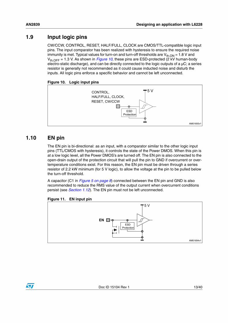
1.9 Input logic pinsCW/CCW, CONTROL, RESET, HALF/FULL, CLOCK are CMOS/TTL-compatible logic input pins. The input comparator has been realized with hysteresis to ensure the required noise immunity is met. Typical values for turn-on and turn-off thresholds are Vth,ON = 1.8 V and Vth,OFF = 1.3 V. As shown in Figure 10, these pins are ESD-protected (2 kV human-body electro-static discharge), and can be directly connected to the logic outputs of a µC; a series resistor is generally not recommended as it could cause inducted noise and disturb the inputs. All logic pins enforce a specific behavior and cannot be left unconnected.
Figure 10. Logic input pins
1.10 EN pinThe EN pin is bi-directional: as an input, with a comparator similar to the other logic input pins (TTL/CMOS with hysteresis), it controls the state of the Power DMOS. When this pin is at a low logic level, all the Power DMOS’s are turned off. The EN pin is also connected to the open-drain output of the protection circuit that will pull the pin to GND if overcurrent or over-temperature conditions exist. For this reason, the EN pin must be driven through a series resistor of 2.2 kW minimum (for 5 V logic), to allow the voltage at the pin to be pulled below the turn-off threshold.
A capacitor (C1 in Figure 5 on page 8) connected between the EN pin and GND is also recommended to reduce the RMS value of the output current when overcurrent conditions persist (see Section 1.12). The EN pin must not be left unconnected.
Figure 11. EN input pin

Designing an application with L6228 AN2839
14/40 Doc ID 15104 Rev 1
1.11 Programmable off time monostableThe L6228 includes a constant off time PWM current controller for each of the two bridges. The current control circuit senses the bridge current by sensing the voltage drop across an external sense resistor connected between the source of the two lower power MOSFET transistors and ground, as shown in Figure 12. As the current in the motor builds up, the voltage across the sense resistor increases proportionally. When the voltage drop across the sense resistor becomes greater than the voltage at the reference input (VrefA or VrefB), the sense comparator triggers the monostable, switching the bridge off. The power MOSFETs remain off for the time set by the monostable, and the motor current recirculates as defined by the selected decay mode, described in the next section. When the monostable times out, the bridge will again turn on. Since the internal dead time used to prevent cross-conduction in the bridge delays the turn-on of the power MOSFETs, the effective off time is the sum of the monostable time plus the dead time.
Figure 12. Simplified schematic of the PWM current controller
Figure 13 on page 15 shows the typical operating waveforms of the output current, the voltage drop across the sensing resistor, the RC pin voltage and the status of the bridge. More details regarding the synchronous rectification and the output stage configuration are included in the next section.
Immediately after the power MOSFET turns on, a high peak current flows through the sensing resistor due to the reverse recovery of the freewheeling diodes. The L6228 provides a 1 µs blanking time, tBLANK, that inhibits the comparator output so that this current spike cannot prematurely re-trigger the monostable.

AN2839 Designing an application with L6228
Doc ID 15104 Rev 1 15/40
Figure 13. Output current regulation waveforms
Figure 14 on page 16 shows the magnitude of the off time tOFF versus the COFF and ROFF values. It can be approximately calculated from the equations:
● tRCFALL = 0.6 · ROFF · COFF
● tOFF = tRCFALL + tDT = 0.6 · ROFF · COFF + tDT
where ROFF and COFF are the external component values and tDT is the internally-generated dead time with:
● 20 kΩ ≤ ROFF ≤ 100 kΩ● 0.47nF ≤ COFF ≤ 100 nF
● tDT = 1 µs (typical value)
Therefore:
● tOFF(MIN) = 6.6 µs
● tOFF(MAX) = 6 ms
These values allow a sufficient range of tOFF to implement the drive circuit for most motors.
The capacitor value chosen for COFF also affects the rise time tRCRISE of the voltage at the pin’s RCA (or RCB). The rise time tRCRISE will only be an issue if the capacitor is not completely charged before the next time the monostable is triggered. Therefore, the on time tON, which depends on the motors and supply parameters, has to be longer than tRCRISE to allow the PWM stage to correctly regulate the current. Furthermore, the on time tON cannot be shorter than the minimum on time tON(MIN).

Designing an application with L6228 AN2839
16/40 Doc ID 15104 Rev 1
Equation 10
Equation 11
1.11.1 Off time selection and minimum on time
Figure 15 shows the lower limit for the on time tON in order to obtain a good PWM current regulation capacity. It has to be said that tON is always longer than tON(MIN) because the device imposes this condition, but it can be shorter than tRCRISE - tDT. In this last case, the device continues to work but the off time tOFF is not more constant.
Therefore, a small COFF value gives more flexibility for the applications (allows a shorter on time and, therefore, a higher switching frequency), but the smaller the value for COFF, the more influential the noises on the circuit performance will be.
1.11.2 Decay modes
The CONTROL input is used to select the behavior of the bridge during the off time. When the CONTROL pin is low, the fast decay mode is selected and both transistors in the bridge are switched off during the off time. When the CONTROL pin is high, the slow decay mode is selected and only the low-side transistor of the bridge is switched off during the off time.
Figure 16 on page 17 shows the operation of the bridge in fast decay mode. At the start of the off time, both power MOSFETs are switched off and the current recirculates through the two opposite freewheeling diodes. The current decays with a high dI/dt since the voltage across the coil is essentially the power supply voltage. After the dead time, the lower power MOSFET in parallel with the conducting diode is turned on in synchronous rectification mode. In applications where the motor current is low, it is possible that the current decays completely to zero during the off time. At this point, if both power MOSFETs were operating in the synchronous rectification mode, it would be possible for the current to build in the opposite direction. To prevent this, only the lower power MOSFET is operated in synchronous rectification mode. This operation is called quasi synchronous rectification. When the monostable times out, the
tON tON MIN( )> 1.5μs (typ. value)=
tON tRCRISE tDT–>⎩⎨⎧
tRCRISE 600 COFF⋅=
Figure 14. Typical off time vs. COFF for several values of ROFF
Figure 15. Minimum on time vs. COFF
AM01697v1
1
10
100
1 . 103
1 . 104
Coff [nF]
tof
f [u
s]
R = 20 kΩ
R = 47 kΩ
R = 100 kΩ
0.1 1 10 100
AM01698v1
1
10
100
Coff [nF]
ton
(m
in)
[u
s]
0.1 1 10 100

AN2839 Designing an application with L6228
Doc ID 15104 Rev 1 17/40
power MOSFETs are turned on again after some delay set by the dead time to prevent cross-conduction.
Figure 17 shows the operation of the bridge in slow decay mode. At the start of the off time, the lower power MOSFET is switched off and the current recirculates around the upper half of the bridge. Since the voltage across the coil is low, the current decays slowly. After the dead time, the upper power MOSFET is operated in the synchronous rectification mode. When the monostable times out, the lower power MOSFET is turned on again after some delay set by the dead time to prevent cross-conduction.
Figure 16. Fast decay mode output stage configurations
Figure 17. Slow decay mode output stage configurations
In some conditions (short off time, very low regulated current, high motor winding L/R) the system may need an on time shorter than 1.5 µs. In such a case, the PWM current controller can lose the regulation.
Figure 18 and Figure 19 on page 18 show the operation of the circuit in this condition. When the current first reaches the threshold, the bridge is turned off for a fixed time and the current decays. During the following on time, the current increases above the threshold, but the bridge cannot be turned off until the minimum 1.5 µs on time has expired. Since the current increases more during each on time than it decays during the off time, it keeps growing during each cycle, with a steady-state asymptotic value set by the duty cycle and load DC resistance.

Designing an application with L6228 AN2839
18/40 Doc ID 15104 Rev 1
The resulting peak current will be:
Equation 12
where D = tON / (tON + tOFF) is the duty cycle and RLOAD is the load DC resistance.
1.12 Overcurrent protectionTo implement an overcurrent protection, a dedicated overcurrent detection (OCD) circuitry (see Figure 20 on page 19 for a simplified schematic) senses the current in each high side. The power DMOS’s are actually made up of thousands of individual identical cells, each carrying a fraction of the total current flowing. The current sensing element, connected in parallel to the power DMOS, is made with only a few such cells, having a 1:N ratio compared to the power DMOS. The total drain current is split between the output and the sense element according to the cell ratio. The sensed current is, then, a small fraction of the output current and will not contribute significantly to power dissipation.
Ipk VSD
RLOAD------------------⋅=
Figure 18. PWM controller loses the current regulation due to minimum on time
Figure 19. PWM controller loses the current regulation due to minimum on time - detail
AM01701v1 AM01702v1

AN2839 Designing an application with L6228
Doc ID 15104 Rev 1 19/40
Figure 20. Simplified circuitry of the overcurrent detection
This sensed current is compared to an internally-generated reference to detect an overcurrent condition. An internal open-drain MOSFET turns on when the sum of the currents in the bridges 1A and 2A or 1B and 2B reaches the threshold (2.8 A typical value); the open drain is internally-connected to the EN pin. To ensure an overcurrent protection, this pin should be connected to an external RC network (Figure 20).
Figure 21 and Figure 22 on page 20 show the device operating in an overcurrent condition (short to ground). When an overcurrent is detected, the internal open-drain MOSFET pulls the EN pin to GND, switching off all 8 power DMOS’s of the device and allowing the current to decay. If an overcurrent conditions persists, like a short to ground or a short between two output pins, the external RC network on the EN pin (see Figure 20) reduces the RMS value of the output current by imposing a fixed disable time after each overcurrent occurrence. The values of REN and CEN are selected to ensure proper operation of the device during a short-circuit condition. When the current flowing through the high-side DMOS reaches the OCD threshold (2.8 A typ.), after an internal propagation delay (tOCD(ON)) the open drain starts discharging CEN. When the EN pin voltage falls below the turn-off threshold (VTH(OFF)), all the power DMOS’s turn off after the internal propagation delay (tD(OFF)EN). The current begins to decay as it circulates through the freewheeling diodes. Since the DMOS’s are off, there is no current flowing through them and no current to sense; therefore, the OCD circuit, after a short delay (tOCD(OFF)), switches the internal open-drain device off, and REN can charge CEN. When the voltage at the EN pin reaches the turn-on threshold (VTH(ON)), after the tD(ON)EN delay, the DMOS’s turn on and the current restarts. Even if the maximum output current can be very high, the external RC network provides a disable time (tDISABLE) to ensure a safe RMS value (see Figure 22).

Designing an application with L6228 AN2839
20/40 Doc ID 15104 Rev 1
The maximum value reached by the current depends on its slew rate, and thus on the state of the short-circuit, the supply voltage, and on the total intervention delay (tDELAY). One can see that after the first current peak, the maximum value reached by the output current decreases; this is because the capacitor on the EN pin is discharged starting from a lower voltage, resulting in a shorter tDELAY.
The following approximate relations estimate the disable time and the first OCD intervention delay after the short-circuit (worst case).
The time the device remains disabled is:
Equation 13
where:
Equation 14
VEN(LOW) is the minimum voltage reached by the EN pin and can be estimated by the relation:
Equation 15
The total intervention time is:
Equation 16
Figure 21. Overcurrent operation: timing 1 Figure 22. Overcurrent operation: timing 2
tDISABLE tOCD OFF( ) tEN RISE( ) tD ON( )EN+ +=
tEN RISE( ) REN CEN
VDD VEN LOW( )–
VDD VTH ON( )–----------------------------------------------------ln⋅ ⋅=
VEN LOW( ) VTH OFF( ) e
tD OFF( )EN tOCD OFF( )+
ROPDR CEN⋅--------------------------------------------------------------------------
⋅=
tDELAY tOCD ON( ) tEN FALL( ) tD OFF( )EN+ +=

AN2839 Designing an application with L6228
Doc ID 15104 Rev 1 21/40
where:
Equation 17
tOCD(OFF), tOCD(ON), tD(ON)EN, tD(OFF)EN and ROPDR are device-intrinsic parameters and VDD is the pull-up voltage applied to REN.
The external RC network, CEN in particular, must be selected to obtain a reasonable fast OCD intervention (short tDELAY) and a safe disable time (long tDISABLE). Figure 23 and Figure 24 show both tDISABLE and tDELAY as a function of CEN: at least 100 µs for tDISABLE are recommended, keeping the delay time between 1 and 2 µs at the same time.
The internal open drain can also be turned on if the device experiences an over-temperature (OVT) condition. The OVT will cause the device to shut down when the die temperature exceeds the OVT threshold (TJ > 165 °C typ.). Since the OVT is also connected directly to the gate-drive circuit (see Figure 1 on page 1), all the Power DMOS’s will shut down, even if the EN pin voltage is still over Vth(OFF). When the junction temperature falls below the OVT turn-off threshold (150 °C typ.), the open drain turns off, CEN is recharged up to VTH(ON) and the Power DMOS’s are turned back on.
1.13 Power managementEven when operating at current levels well below the maximum ratings of the device, the operating junction temperature must be kept below 125° C.
Figure 25 on page 22 shows the IC’s dissipated power versus the RMS load current in four different driving sequences, assuming the supply voltage is 24 V.
tEN FALL( ) ROPDR CEN
VDDVTH OFF( )------------------------------ln⋅ ⋅=
Figure 23. Typical disable time vs. CEN for several values of REN
Figure 24. Typical delay time vs. CEN
AM01706v1
0010111
1 0
1 0 0
1 .1 03
C E N [ n F ]
t DIS
AB
LE [µ
s]
R E N = 2 2 0 kΩ R E N = 1 0 0 kΩR E N = 4 7 kΩR E N = 3 3 kΩ
R E N = 1 0 kΩ

Designing an application with L6228 AN2839
22/40 Doc ID 15104 Rev 1
Figure 25. IC dissipated power versus output current

AN2839 Designing an application with L6228
Doc ID 15104 Rev 1 23/40
1.13.1 Maximum output current versus selectable devices
Figure 26 shows a performance comparison between the L6228 (standard power) and the L6208 (high power) for different packages, with the following assumptions.
● Normal drive mode (two-phase on).
● Supply voltage: 24 V; switching frequency: 30 kHz.
● Tamb = 25° C, TJ = 125° C.
● Maximum RDS(on) (taking into account the process spread) considered, at 125° C.
● Maximum quiescent current IQ (taking into account the process spread) considered.
● PCB is an FR4 with a dissipating copper surface on the top side of 6 cm2 (with a thickness of 35 µm) for SO and PowerDIP packages (D, N suffixes).
● PCB is an FR4 with a dissipating copper surface on the top side of 6 cm2 (with a thickness of 35 µm), 16 via holes and a ground layer for the PowerSO package (PD suffix).
For each device (on the x axis), the y axis reports the maximum output current.
Figure 26. Maximum output current vs. selectable devices
1.13.2 Power dissipation and thermal analysis with PractiSPINTM software
The PractiSPINTM software includes a power dissipation and thermal analysis section that helps to calculate the IC power dissipation and estimate its junction temperature through a simulation.
The purpose of this section is to help perform a quick evaluation of the device, package and dissipating copper area required by the user’s application, and is a good starting point when designing an application (from the power dissipation and thermal points of view). Software results, especially thermal results, need to be confirmed on-bench.

Designing an application with L6228 AN2839
24/40 Doc ID 15104 Rev 1
The input data for simulation is divided in three sections.
● Application data: to select the motor characteristics and its configuration, the driving parameters and the analysis type (steady state, single pulse or repeated pulse analysis)
● Device data: to choose the device part number and edit some available IC parameters.
● PCB data: to select the package, PCB dissipating characteristics and ambient temperature
The output data includes the temperature and current profile waveforms, the estimated IC power dissipation and junction temperature.
For more details on the formulas used in the software, refer to the "Help" menu of the power dissipation and thermal analysis window.
Figure 27. Power dissipation and thermal analysis with PractiSPINTM software
1.14 Choosing the decay modeThe L6228 can operate in either fast or slow decay mode, each having a specific recirculation path for the current during off time. In slow decay mode, only the lower DMOS is turned off and the current recirculates around the upper half of the bridge so that the voltage across the coil is close to zero. In fast decay mode, both DMOS’s are turned off and the current recirculates back to the power supply rail so that the voltage across the coil is essentially the power supply voltage itself.
Slow decay operation provides several advantages: for a given peak current and off time, the current ripple is minimized. The same is true for acoustic noise and losses in the motor iron (achieving the same current ripple with fast decay mode would require a shorter off time resulting in a higher switching frequency and higher power dissipation in the IC). As current recirculates in the upper half of the bridge and both high-side DMOS’s in the same bridge are on, synchronous rectification is realized, minimizing power dissipation in the power switches. Furthermore, since no output pin goes below GND (see Section 1.2), no power is dissipated on the sense resistor during the off time (see Section 1.5).
AM01710v1

AN2839 Designing an application with L6228
Doc ID 15104 Rev 1 25/40
On the other hand, slow decay can be undesirable in some situations, for example when current has to be regulated at very low values or the motor winding L/R ratio is high. In these cases, an on time shorter than the minimum tON (about 1.5 µs) may be requested to regulate the current, and this can cause the PWM controller to lose the regulation (refer to Section 1.11).
Another situation where fast decay should be preferred to slow decay is when the regulated current is expected to vary over time with a given profile (enforced, providing a variable voltage on the Vref pins - see Section 1.16). Here fast decay helps to track fast decreasing edges in the desired profile.
1.15 Choosing the stepping sequenceThe device can provide three different sequences to run a stepper motor: full-step, two-phase on (normal drive), full-step, one-phase on (wave drive) and half-step.
If half-step driving is used, the motor advances by half a step after each clock pulse, obtaining a higher position resolution and reducing instability due to low torque regions in certain motors' speed-torque diagrams, when used in full-step mode.
Figure 28. Torque instability in full-step mode.
When this driving method is used, the torque is affected by ripple because in odd-numbered states, when both coils are driven, the total current in the motor windings is double that found in even-numbered states.
A way to avoid the high torque ripple in half-step mode is to supply the motor with a higher current (by a factor of ) during the even-numbered states, in which only one winding is energized, simply by applying a higher reference voltage at the VrefA, VrefB pins during these states (see Figure 29 on page 26)(b).
b. Also refer to [2] in References.
22

Designing an application with L6228 AN2839
26/40 Doc ID 15104 Rev 1
Figure 29. Balanced half step for low torque ripple
A simple circuit to generate two different reference voltages is shown in Figure 30. R1 and R2 should be chosen to have:
Equation 18
and R3 should be:
Equation 19
A similar circuit can also be used to modify the reference voltage in other situations. For example, it is possible at a constant rotation speed to reduce the motor torque and to increase it during acceleration and deceleration. A second transistor can be added to implement four different reference voltages, selectable by two logic signals.
Figure 30. Realizing half-step current shaping
Normal and wave drive are full-step modes. In wave drive mode, the two motor windings are alternately energized, while in normal drive, both the windings are energized in each state, increasing the torque by a factor of . On the other hand, the total current in the motor is double, so the efficiency is similar. In wave drive mode, the torque ripple is higher than in normal drive mode.
Vref HIGH, Vref 2⋅ 5VR2
R1 R2+----------------------⋅= =
R3
R1 R2⋅
2 1–( ) R1 R2+( )⋅-----------------------------------------------------=
AM01713v1
5V duringodd numbered states
0V duringeven numbered states
GND
+5V
R1
R2
R3
4.7kΩ
15kΩ
to Vref pin(s)
2

AN2839 Designing an application with L6228
Doc ID 15104 Rev 1 27/40
1.16 MicrosteppingMicrostepping operation has several advantages, including the absence of any instability phenomena due to low torque regions in certain motors' speed-torque diagrams (see Figure 28 on page 25), reduction of mechanical noise and increased position resolution. The L6228 can be used as a two-phase microstepping driver IC(c). The controller’s circuitry allows for an easy and inexpensive design with such a device. By controlling the Vref inputs, it is possible to obtain in the two phases variable output currents with a sine wave shape. A variable voltage proportional to the desired output current is applied to each reference pin. For microstepping, the two inputs are rectified sine-wave voltages with a phase delay of 90°. The L6228 is operated in the normal drive mode and the frequency of the two sine wave voltages must be 1/4 of the CLOCK frequency. Figure 31 shows a circuit to generate the two sine wave signals using low-pass filters and two PWM outputs of a µC (see Section 1.8). Figure 32 shows the Vref voltages, the CLOCK signal and the output currents.
Figure 31. Microstepping application
Figure 32. Microstepping reference voltages, output currents and CLOCK signal
The slow decay mode can sometimes be inadequate, particularly at high rotation speeds, since it does not allow the motor current to decay quickly enough and follow the decreasing
c. Refer to [5] in References.

Designing an application with L6228 AN2839
28/40 Doc ID 15104 Rev 1
slope of the desired sine wave. In cases like this, the fast decay mode can just be applied during the negative slope of the current (Figure 33).
The disadvantage is an increased current ripple in the other winding (where the current is increasing and fast decay is not needed).
Figure 33. Using fast decay during a high, negative current slope
AM01716v1

AN2839 Application example
Doc ID 15104 Rev 1 29/40
2 Application example
The first step is to select the type of decay. For the purpose of this example, we will implement slow decay, which allows a lower power dissipation, lower ripple and avoids voltages below GND at the output pins during recirculation.
The power dissipation and thermal analysis PractiSPINTM tool allow calculation of the IC power dissipation and estimation of the junction temperature. The purpose of this section is to help perform a fast evaluation of the device, package and dissipating copper area required by the user’s application, and is intended as a good starting point when designing an application (from the power dissipation and thermal points of view). Software results, especially thermal results, need to be confirmed on-bench.
The bulk capacitor needs to withstand at least 24 V + 5% + 25% ≅ 32 V. A 50 V capacitor will be used. Allowing a voltage ripple of 200 mV, the capacitor’s ESR should be lower than 200 mV/0.5 A = 400 mΩ; the AC current capability should be about 0.5 A.
Providing a reference voltage of 0.5 V, 1-Ω sensing resistors are needed. In slow decay mode, the resistors’ power rating is approximately PR ≅ Irms
2 · RSENSE · D ≅ 0.25 W.A 1 Ω - 0.25 W - 1% resistor is used. The charge pump uses recommended components (1N4148 diodes, ceramic capacitors and a 100 Ω resistor to reduce EMI).
R = 18 kΩ, C = 1.2 nF are connected to the RC pins, obtaining tOFF ≅ 16 µs. A 5.6 nF capacitor has been placed on the EN pin, and the pin is driven by the µC through a 100-kΩ resistor. With these values, if there is a short-circuit between two OUT pins or an OUT pin and GND, the power DMOS’s turn off after approximately 1 µs, and tDISABLE ≅ 240 µs.
Table 2. Application data
Application data Value
Rotation speed 300 rpm (fCK = 1 kHz)
Winding peak current 1 A
Maximum ripple 50 mA
Supply voltage 24 V ± 5%
Sequence Wave mode
Table 3. Motor data
Motor data Value
Winding resistance 6.6 Ω
Winding inductance 7.9 mH
Step angle 1.8°/step
Maximum BEMF at 300 rpm 15 V

Application example AN2839
30/40 Doc ID 15104 Rev 1
Figure 34. Application example
With wave drive selected, the dissipating power is about 0.8 W. If the ambient temperature is lower than 50° C, with a 4 cm2 copper area on the PCB and an SO24 package, the estimated junction temperature is about 94° C. Using more copper area or a PowerDIP package will reduce the junction temperature.
AM01717v1

AN2839 Demonstration board
Doc ID 15104 Rev 1 31/40
Appendix A Demonstration board
A.1 PractiSPINTM
PractiSPINTM is an evaluation and demonstration system that can be used with the powerSPINTM family (L62xx) of devices. A graphical user interface (GUI) program (shown in Figure 35) runs on an IBM PC under Windows and communicates with a common ST7-based interface board (Figure 36 on page 32) through the RS-232 serial port. The ST7 interface board connects to a device-specific demonstration board (target board) via a standard 34-pin ribbon cable interface.
Depending on the target device, the PractiSPINTM can drive a stepper motor, 1 or 2 DC motors or a brushless DC (BLDC) motor, operating significant parameters such as speed, current, voltage, direction, acceleration and deceleration rates from a user-friendly graphic interface, and programming a sequence of movements.
The software can also evaluate the power dissipated by the selected device and, for a given package and dissipating copper area on the PCB, estimate the device's junction temperature.
Figure 35. PractiSPINTM PC software
AM01718v1

Demonstration board AN2839
32/40 Doc ID 15104 Rev 1
Figure 36. PractiSPINTM ST7 demonstration board
A.2 L6228N evaluation with EVAL6208NTo easily evaluate the device in PowerDIP packages, it is possible to use the EVAL6208N, replacing the device directly on the available socket.
We recommend changing the sense resistor values to manage lower load currents according to the device’s specifications.
The EVAL6208N’s electrical schematic is shown in Figure 37 on page 33. For more information, refer to AN1451 "L6208 fully-integrated two-phase stepper motor driver".
A.2.1 Important notes
● JP1: should be closed in the INT position for use with the PractiSPINTM ST7 board.
● C6: recommended change to 5.6 nF for safe overcurrent protection.
● R8: recommended change to 100 kΩ for safe overcurrent protection.
● R9: recommended change to 100 kΩ if EN pin is driven from the CN5 connector (for example with PractiSPINTM ST7 board) for safe overcurrent protection.
● R20, R24: set the maximum current obtainable through PractiSPINTM (see PractiSPINTM documentation).
● R2: recommended change to adequate value (depending on supply voltage) to obtain 5 V across D3.

AN2839 Demonstration board
Doc ID 15104 Rev 1 33/40
Figure 37. EVAL6208N electrical schematic

Demonstration board AN2839
34/40 Doc ID 15104 Rev 1
A.3 EVAL6228QRA demonstration board has been designed to help in the evaluation of the device in QFN packages. The board implements a typical application that can be used as a reference design to drive a two-phase bipolar stepper motor with currents up to 1 A DC.
Thanks to the L6228Q’s small footprint (QFN 5 x 5 mm 32 leads), the PCB is very compact (27 x 32 mm).
Figure 42 on page 37 shows the electrical schematic of the board. Table 4 reports the parts list.
Figure 38. EVAL6228QR
A step clock input is used to apply a clock signal that determines the progress of the internal state machine. It can be reset to its initial state by pulling down the reset line.
To perform the PWM current control, an analog reference voltage should be provided to each of the driver’s channels. A fixed reference voltage can be easily obtained through a
Table 4. EVAL6228QR parts list
Part reference Part value Part description
C1 220 nF/25 V Capacitor
C2 220 nF/63 V Capacitor
C3 100 µF/63 V Capacitor
C4 10 nF/25 V Capacitor
C5 5.6 nF Capacitor
C6, C6 820 pF Capacitor
C8, C9 220 nF Capacitor
D1 BAT46SW Diodes
R1, R2, R3, R4, R5, R8 100 kΩ 5% 0.25 W Resistor
R6, R7 100kΩ 1% 0.25 W Resistor
R9, R10 0.4 Ω 1 W Resistor
R11, R13 20 kΩ 1% 0.25 W Resistor
R12, R14 2 kΩ 1% 0.25 W Resistor
U1 L6228Q Stepper motor driver in VFQFPN5x5

AN2839 Demonstration board
Doc ID 15104 Rev 1 35/40
resistive divider from an external voltage rail and GND (possibly the one supplying the µC or the rest of the application).
Otherwise, a very simple way to obtain a variable voltage without using a DAC is to low-pass filter a PWM output of a µC.
The input lines CW/CCW, control, half/full, EN and reset are connected to ground through a pull-down resistor which sets as default the low logic level on these lines. An external signal can be applied to change each input status.
D1, C1 and C4 make up a charge-pump circuit, which generates the supply voltage for the high-side integrated MOSFETs. Due to voltage and current switching at relatively high frequencies, these components are connected together through short paths in order to minimize induced noise on other circuitries.
R1 and C5 are used by the overcurrent protection’s integrated circuitry (the disable time tDISABLE is about 200 µs and delay time tDELAY about 1 µs with the values in Table 4).
R6, C6 and R7, C7 are used to set the off time tOFF of the two PWM channels at about 50 µs. The off time should be adjusted according to the motor’s electrical characteristics and supply voltage by changing the R6, C6 and R7, C7 values.
R11, R12, C8 and R13, R14, C9 are low-pass filters used to provide an external reference voltage through a PWM output of a µC.
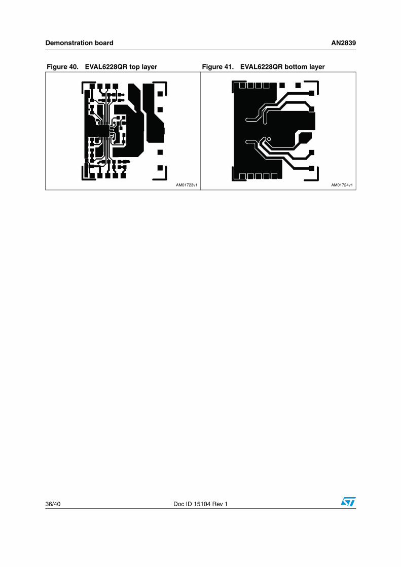
Figure 39 and Figure 41 show the components’ placement and the two layers of the EVAL6228QR reference design board. A GND area has been used to improve the IC’s power dissipation.
Figure 39. EVAL6228QR component placement
Demonstration board AN2839
36/40 Doc ID 15104 Rev 1
Figure 40. EVAL6228QR top layer Figure 41. EVAL6228QR bottom layer

AN2839 Demonstration board
Doc ID 15104 Rev 1 37/40
Figure 42. EVAL6228QR electrical schematic

References AN2839
38/40 Doc ID 15104 Rev 1
References
1. "A New Fully Integrated Stepper Motor Driver IC", Proceedings of PCIM 2001, September 2001, Intertech Communication.
2. "Stepper Motor Driving" (AN235).
3. "Controlling Voltage Transients in Full Bridge Driver Applications" (AN280).
4. "Stepper Motor Drive Considerations, Common Problems and Solutions" (AN460).
5. "Microstepping Stepper Motor Drive Using Peak Detecting Current Control" (AN1495).
6. "A New High Power IC Surface Mount Package Family" (AN668).

AN2839 Revision history
Doc ID 15104 Rev 1 39/40
Revision history
Table 5. Document revision history
Date Revision Changes
22-Sep-2009 1 Initial release.

AN2839
40/40 Doc ID 15104 Rev 1
Please Read Carefully:
Information in this document is provided solely in connection with ST products. STMicroelectronics NV and its subsidiaries (“ST”) reserve theright to make changes, corrections, modifications or improvements, to this document, and the products and services described herein at anytime, without notice.
All ST products are sold pursuant to ST’s terms and conditions of sale.
Purchasers are solely responsible for the choice, selection and use of the ST products and services described herein, and ST assumes noliability whatsoever relating to the choice, selection or use of the ST products and services described herein.
No license, express or implied, by estoppel or otherwise, to any intellectual property rights is granted under this document. If any part of thisdocument refers to any third party products or services it shall not be deemed a license grant by ST for the use of such third party productsor services, or any intellectual property contained therein or considered as a warranty covering the use in any manner whatsoever of suchthird party products or services or any intellectual property contained therein.
UNLESS OTHERWISE SET FORTH IN ST’S TERMS AND CONDITIONS OF SALE ST DISCLAIMS ANY EXPRESS OR IMPLIEDWARRANTY WITH RESPECT TO THE USE AND/OR SALE OF ST PRODUCTS INCLUDING WITHOUT LIMITATION IMPLIEDWARRANTIES OF MERCHANTABILITY, FITNESS FOR A PARTICULAR PURPOSE (AND THEIR EQUIVALENTS UNDER THE LAWSOF ANY JURISDICTION), OR INFRINGEMENT OF ANY PATENT, COPYRIGHT OR OTHER INTELLECTUAL PROPERTY RIGHT.
UNLESS EXPRESSLY APPROVED IN WRITING BY AN AUTHORIZED ST REPRESENTATIVE, ST PRODUCTS ARE NOTRECOMMENDED, AUTHORIZED OR WARRANTED FOR USE IN MILITARY, AIR CRAFT, SPACE, LIFE SAVING, OR LIFE SUSTAININGAPPLICATIONS, NOR IN PRODUCTS OR SYSTEMS WHERE FAILURE OR MALFUNCTION MAY RESULT IN PERSONAL INJURY,DEATH, OR SEVERE PROPERTY OR ENVIRONMENTAL DAMAGE. ST PRODUCTS WHICH ARE NOT SPECIFIED AS "AUTOMOTIVEGRADE" MAY ONLY BE USED IN AUTOMOTIVE APPLICATIONS AT USER’S OWN RISK.
Resale of ST products with provisions different from the statements and/or technical features set forth in this document shall immediately voidany warranty granted by ST for the ST product or service described herein and shall not create or extend in any manner whatsoever, anyliability of ST.
ST and the ST logo are trademarks or registered trademarks of ST in various countries.
Information in this document supersedes and replaces all information previously supplied.
The ST logo is a registered trademark of STMicroelectronics. All other names are the property of their respective owners.
© 2009 STMicroelectronics - All rights reserved
STMicroelectronics group of companies
Australia - Belgium - Brazil - Canada - China - Czech Republic - Finland - France - Germany - Hong Kong - India - Israel - Italy - Japan - Malaysia - Malta - Morocco - Philippines - Singapore - Spain - Sweden - Switzerland - United Kingdom - United States of America
www.st.com