an2714, optimizing the instruction cache of starcore...
TRANSCRIPT
Freescale SemiconductorApplication Note
AN2714Rev. 1, 11/2004
CONTENTS
1 Instruction Cache Basics .........................................21.1 Locality ...................................................................41.2 Types of Cache Misses ...........................................42 Extended Core Basics .............................................52.1 M1 Memory ............................................................62.2 Instruction Cache ....................................................73 Optimizing Code Performance ................................83.1 Cache Performance Characteristics ........................83.2 Code Optimization ..................................................93.3 System-Level Optimizations .................................103.4 Procedural-Level Optimizations ...........................153.5 Algorithmic-Level Optimizations .........................194 Conclusions........................................................... 215 References .............................................................23
Optimizing the Instruction Cache of StarCore™-Based Processorsby Hezi Rahamim
Although microprocessor speeds have dramatically increased in recent years, improvements in the access times of standard system memory such as SDRAM or DDR have proceeded much more slowly. The gap between microprocessor speed and memory access speed is increasing to such an extent that unless we can reduce memory access latencies, future improvements in CPU speeds will be increasingly nullified by the time taken to retrieve data from memory. The main technique to reduce memory access time is a cache hierarchy. Although accessing data in the first-level cache, which is the cache closest to the processor, does not carry much of a performance penalty, the required data will probably not be in the cache because the cache is so small. The result is a cache miss that causes the processor to stall until the desired data can be brought in from a higher level of the memory hierarchy. Cache misses are a common cause of CPU stalls and therefore limit performance. Reducing the numbers of stalls significantly improves overall system speeds. This application note describes how to write code to minimize the number of cache stalls. It explains how to use the cache environment of the SC140 extended core with maximum efficiency.
Note: The SC140 and SC1400 cores are functionally identical and code-compatible. The information in this document applies to both cores. For simplicity, the SC140 core is referenced throughout this application note. StarCore™-based products to which this application note applies are the MSC7110, MSC7112, MSC7113, MSC7115, MSC7116, MSC8102, MSC8122, and MSC8126.
© Freescale Semiconductor, Inc., 2004. All rights reserved.
Instruction Cache Basics
1 Instruction Cache BasicsUnlike general-purpose processors, most DSPs do not have a cache. Instead, they rely on multiple banks of on-chip memory and multiple bus sets to allow for several memory accesses per instruction cycle. However, some DSPs do incorporate a small, specialized instruction cache for storing instructions in small loops so that the internal bus sets can be free to retrieve data words. The increasingly high DSP clock rates enable DSPs to process more and more application channels for voice compression, video compression in wireless baseband applications, and packet telephony applications. Multi-channel processing usually requires both an increase in internal memory and multi-core solutions. The instruction and data caches isolate the multi-core platform and the internal memory from the core, therefore maintaining a high clock rate to the core without significantly affecting application performance. The result is a significant decrease in expensive zero wait state memory and therefore DSP processor die area. In addition, the level of associativity and the high cache hit rate usually require almost no optimization, thus shortening code development and accelerating time to market.
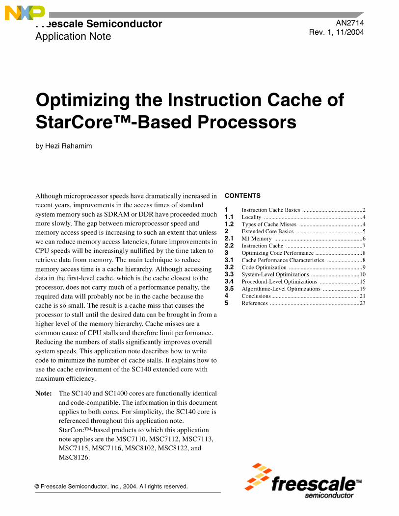
Caches can be either direct-mapped or N-way set1 associative. In a direct mapped cache, each main memory line has only one possible location in the cache according to its index. Figure 1 shows the internal structure and operation flow of a direct-mapped cache.
Figure 1. Structure of a Direct-Mapped Cache
1. A set is sometimes called an index.
CPUAddress
DataIn Out
Tag Index
Tag DataValid
4:1 Multiplex
Line AddressLine Offset
1
2
3
4
=?
Lower-Level Memory
Data
Optimizing the Instruction Cache of StarCore™-Based Processors, Rev. 1
2 Freescale Semiconductor

Instruction Cache Basics
Figure 2 shows the internal structure of the instruction cache (ICache) in the SC140 extended core, which is a 16-way set associative cache. Each main memory line has 16 different possible locations in the cache. The valid bit resolution (VBR) is 128 bits, and there is a valid bit for every 16-byte fetch set.
The SC140 extended core uses prefetching to prevent cache misses. A prefetch operation is added to the normal processor memory access instructions. Instead of fetching data on a cache miss, prefetching anticipates these misses and issues a fetch to the memory system before the actual memory reference. This prefetch occurs in parallel with normal processor operations, allowing the memory system time to transfer the data from main memory to the cache. Ideally, the prefetch process completes just as the processor needs to access the required data, without stalling the processor. In a non-blocking prefetch system, more prefetches can be issued while the first one is occurring.
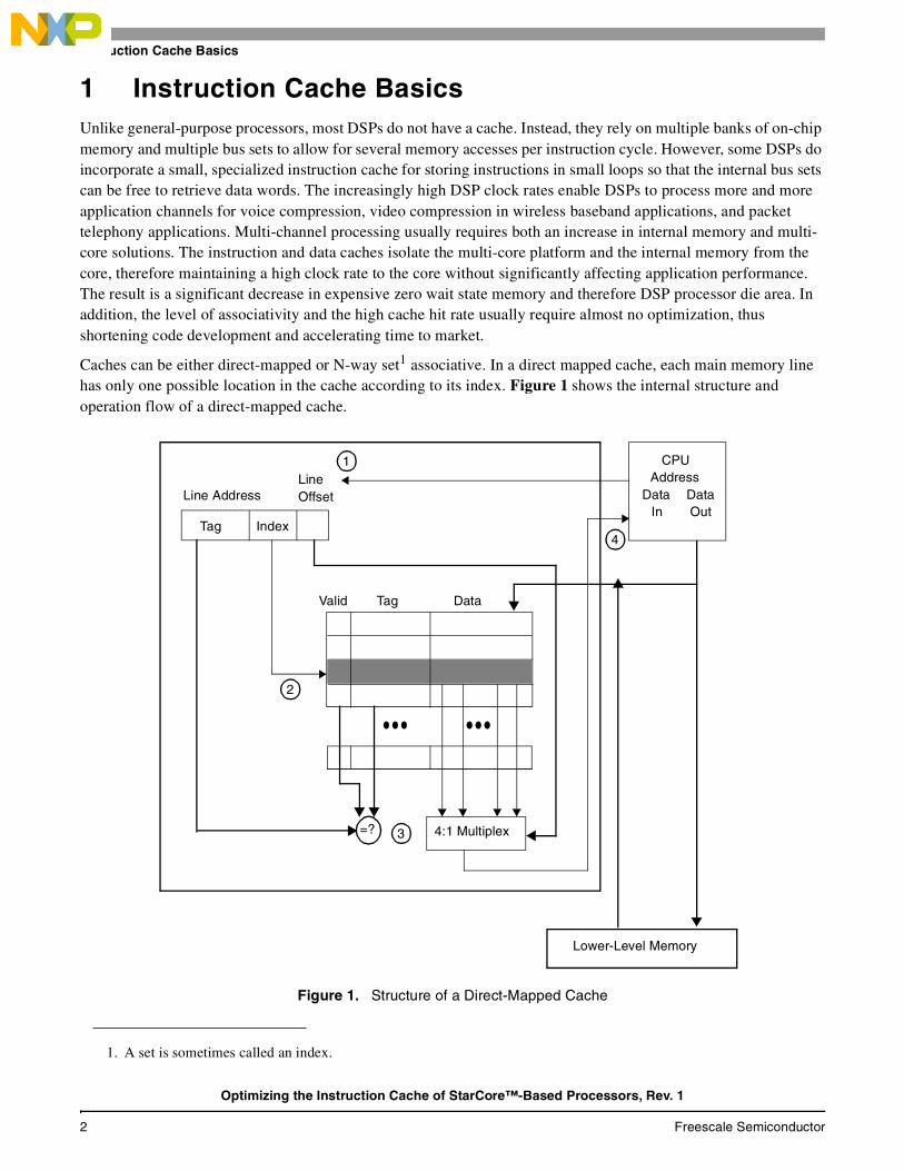
Figure 3 shows the line prefetch mechanism of the SC140 extended core. In this example, a miss occurs in an address corresponding to the sixth valid bit. First, the miss is served and VBR number 6 is fetched from the memory to the cache (marked by a circle). Then the rest of the burst is fetched to the cache in a wrap-around order. When the missed burst finishes, the prefetch mechanism continues fetching data into the cache until the end of the line or until a new miss occurs.
Figure 2. Structure of N-way Set Associative Cache
0000Fetch SetINDEXTAG
TAGValid Bits
One Per Fetch SetLine
256 Bytes
Way 0: Index 0
Way 0: Index 1
Way 0: Index 2
Way 0: Index 3
Way 1: Index 0
Way 1: Index 1
Way 1: Index 2
Way 1: Index 3
Way 15: Index 0
Way 15: Index 1
Way 15: Index 2
Way 15: Index 3
31 10 9 8 7 4 3 0
Optimizing the Instruction Cache of StarCore™-Based Processors, Rev. 1
Freescale Semiconductor 3
Instruction Cache Basics
Figure 3. Line Prefetch
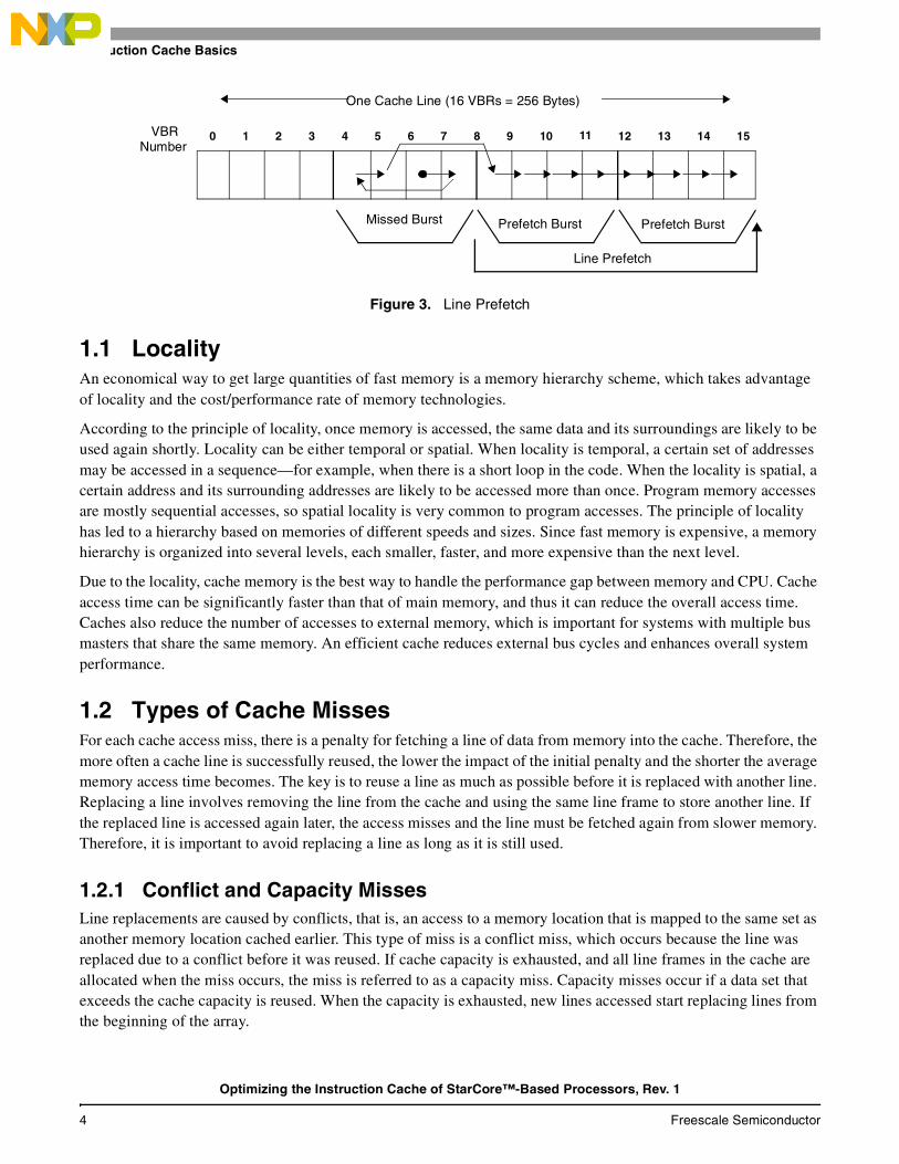
1.1 LocalityAn economical way to get large quantities of fast memory is a memory hierarchy scheme, which takes advantage of locality and the cost/performance rate of memory technologies.
According to the principle of locality, once memory is accessed, the same data and its surroundings are likely to be used again shortly. Locality can be either temporal or spatial. When locality is temporal, a certain set of addresses may be accessed in a sequence—for example, when there is a short loop in the code. When the locality is spatial, a certain address and its surrounding addresses are likely to be accessed more than once. Program memory accesses are mostly sequential accesses, so spatial locality is very common to program accesses. The principle of locality has led to a hierarchy based on memories of different speeds and sizes. Since fast memory is expensive, a memory hierarchy is organized into several levels, each smaller, faster, and more expensive than the next level.
Due to the locality, cache memory is the best way to handle the performance gap between memory and CPU. Cache access time can be significantly faster than that of main memory, and thus it can reduce the overall access time. Caches also reduce the number of accesses to external memory, which is important for systems with multiple bus masters that share the same memory. An efficient cache reduces external bus cycles and enhances overall system performance.
1.2 Types of Cache MissesFor each cache access miss, there is a penalty for fetching a line of data from memory into the cache. Therefore, the more often a cache line is successfully reused, the lower the impact of the initial penalty and the shorter the average memory access time becomes. The key is to reuse a line as much as possible before it is replaced with another line. Replacing a line involves removing the line from the cache and using the same line frame to store another line. If the replaced line is accessed again later, the access misses and the line must be fetched again from slower memory. Therefore, it is important to avoid replacing a line as long as it is still used.
1.2.1 Conflict and Capacity MissesLine replacements are caused by conflicts, that is, an access to a memory location that is mapped to the same set as another memory location cached earlier. This type of miss is a conflict miss, which occurs because the line was replaced due to a conflict before it was reused. If cache capacity is exhausted, and all line frames in the cache are allocated when the miss occurs, the miss is referred to as a capacity miss. Capacity misses occur if a data set that exceeds the cache capacity is reused. When the capacity is exhausted, new lines accessed start replacing lines from the beginning of the array.
0 151 2 3 4 5 6 7 8 9 10 11 12 13 14
One Cache Line (16 VBRs = 256 Bytes)
VBRNumber
Missed Burst Prefetch Burst Prefetch Burst
Line Prefetch
Optimizing the Instruction Cache of StarCore™-Based Processors, Rev. 1
4 Freescale Semiconductor
Extended Core Basics
Identifying the cause of a miss may help you to choose the appropriate way to avoid the miss. Conflict misses mean that the data accessed fits into the cache but lines are evicted due to conflicts. In this case, we may want to change the memory layout so that the data accessed is located at addresses in memory that do not conflict (map to the same set) in the cache. For capacity misses, you should reduce the amount of data that is processed at any given time.
1.2.2 Compulsory MissesA third category of misses is compulsory or first reference misses, which occur when the data is brought into the cache for the first time. A prefetch can reduce the amount of compulsory misses by predicting the program flow and then fetching the relevant instruction before it is accessed.
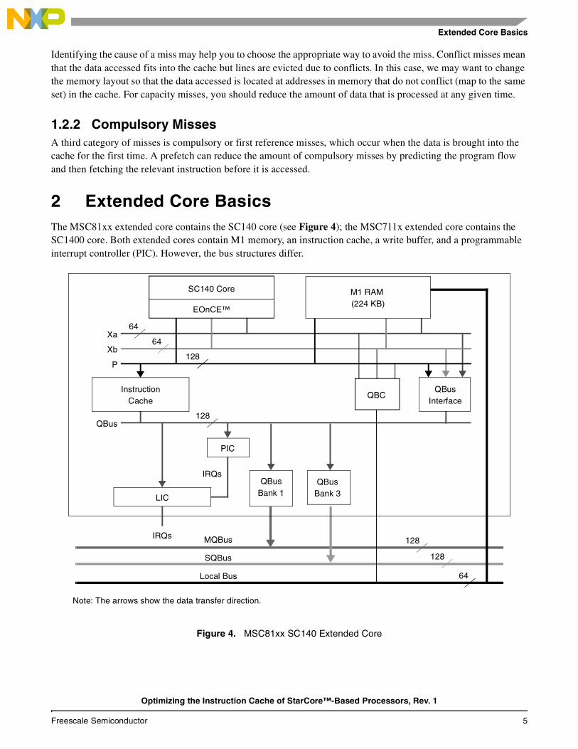
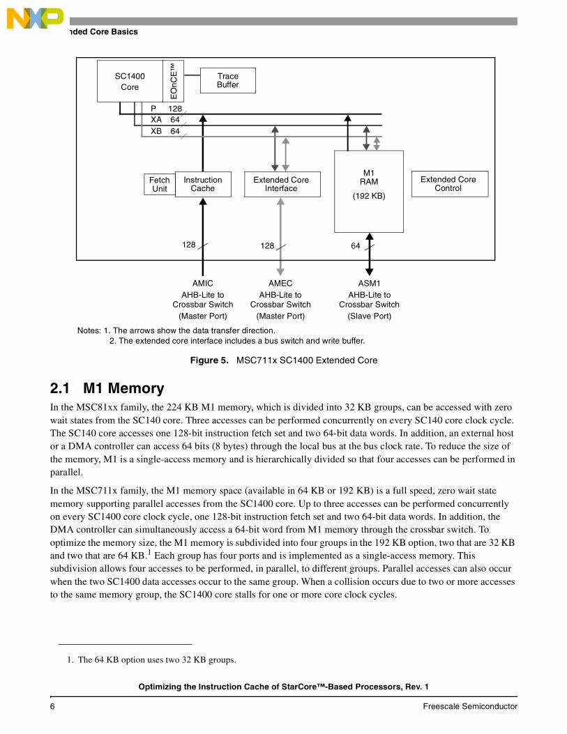
2 Extended Core BasicsThe MSC81xx extended core contains the SC140 core (see Figure 4); the MSC711x extended core contains the SC1400 core. Both extended cores contain M1 memory, an instruction cache, a write buffer, and a programmable interrupt controller (PIC). However, the bus structures differ.
Figure 4. MSC81xx SC140 Extended Core
Xa
Xb
P
QBus
IRQs
IRQs
MQBus
SQBus
Local Bus
128
128
64
64
64
LIC
PIC
128
128
SC140 Core
EOnCE™
QBusInterface
InstructionCache
M1 RAM (224 KB)
Note: The arrows show the data transfer direction.
QBusBank 1
QBusBank 3
QBC
Optimizing the Instruction Cache of StarCore™-Based Processors, Rev. 1
Freescale Semiconductor 5
Extended Core Basics
Figure 5. MSC711x SC1400 Extended Core
2.1 M1 MemoryIn the MSC81xx family, the 224 KB M1 memory, which is divided into 32 KB groups, can be accessed with zero wait states from the SC140 core. Three accesses can be performed concurrently on every SC140 core clock cycle. The SC140 core accesses one 128-bit instruction fetch set and two 64-bit data words. In addition, an external host or a DMA controller can access 64 bits (8 bytes) through the local bus at the bus clock rate. To reduce the size of the memory, M1 is a single-access memory and is hierarchically divided so that four accesses can be performed in parallel.
In the MSC711x family, the M1 memory space (available in 64 KB or 192 KB) is a full speed, zero wait state memory supporting parallel accesses from the SC1400 core. Up to three accesses can be performed concurrently on every SC1400 core clock cycle, one 128-bit instruction fetch set and two 64-bit data words. In addition, the DMA controller can simultaneously access a 64-bit word from M1 memory through the crossbar switch. To optimize the memory size, the M1 memory is subdivided into four groups in the 192 KB option, two that are 32 KB and two that are 64 KB.1 Each group has four ports and is implemented as a single-access memory. This subdivision allows four accesses to be performed, in parallel, to different groups. Parallel accesses can also occur when the two SC1400 data accesses occur to the same group. When a collision occurs due to two or more accesses to the same memory group, the SC1400 core stalls for one or more core clock cycles.
1. The 64 KB option uses two 32 KB groups.
XB
AHB-Lite to
128
64
SC1400
EO
nCE
™Extended Core
InterfaceInstruction
Cache
M1RAM
Notes: 1. The arrows show the data transfer direction.2. The extended core interface includes a bus switch and write buffer.
FetchUnit
128 64
Crossbar SwitchAHB-Lite to
Crossbar SwitchAHB-Lite to
Crossbar Switch
XA 64P 128
(192 KB)
Core
(Master Port) (Master Port) (Slave Port)
AMIC ASM1AMEC
Extended CoreControl
TraceBuffer
Optimizing the Instruction Cache of StarCore™-Based Processors, Rev. 1
6 Freescale Semiconductor
Extended Core Basics
Intelligent memory allocation significantly decreases the probability of collisions between an SC140 core bus and the DMA bus. For example, two accesses cannot collide if they belong to different 32 KB memory groups, which is usually the case since program code is stored in a different group than the data space of the program. The DMA controller stores the “next” buffers in yet a different group. Even in the same group, if two data elements are placed on a different module, a collision between two SC140 core buses is prevented. When a collision does occur, the SC140 core stalls for one clock cycle.
The overall memory size available for one SC140 core in both M1 and M2 memories and the partition between the memories is carefully designed as a trade-off between chip size and the memory requirements imposed by the bandwidth of the SC140 core. Typically the M1 memory contains critical routines and most of the channel data.
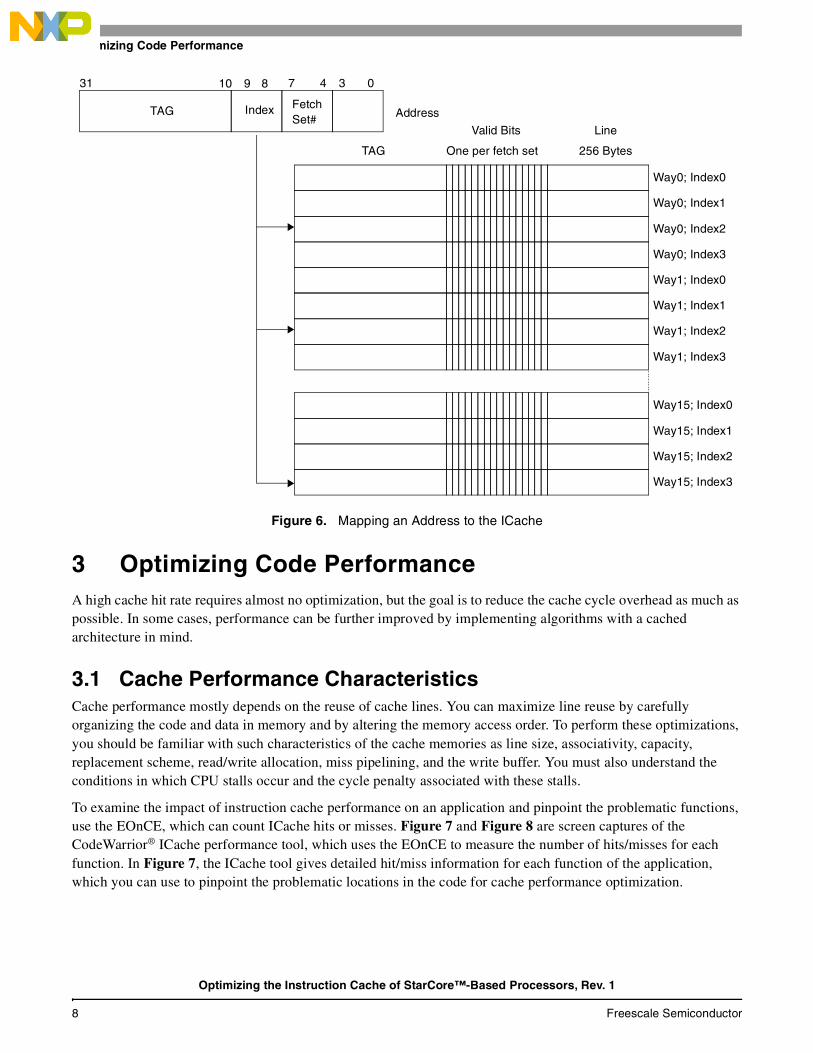
2.2 Instruction CacheThe SC140 ICache is highly optimized for real-time DSP applications and minimizes miss ratios, latencies, bus bandwidth requirements, and silicon area. The 16 KB ICache is 16-way set associative. Figure 6 illustrates its logic structure and demonstrates how an address is mapped to this structure. Each of the 16 ways contains four 256-byte lines and is divided into 16 fetch sets, each with an associated valid bit. The 2-bit index field of the address serves as an index to the line within the way. The line whose tag matches the tag field of the address is the selected line.
When a cache miss occurs, the new data is fetched in bursts of 1, 2, or 4 fetch sets (the MSC8102 DSP can fetch instructions in bursts of one fetch set only). There is also an option to fetch until the end of the line. This option, referred to as prefetch, takes advantage of the spatial locality of the code. When there is a need to fetch new data to the cache and the cache is full, one of the lines of the cache is thrashed using the least recently used (LRU) algorithm. The cache can be programmed so that only part of it is thrashed. For example, suppose task A needs to be preempted in favor of task B. While task B runs, the instructions of task A are thrashed from the instruction cache. When task B finishes and task A takes over, task A may find that its most recently used instructions are not in the cache. To prevent such a situation and thus keep task A’s most recently used instructions in the cache, the operating system can exclude the ways of task A from the part of the cache that can be thrashed. Another method of guaranteeing that the critical routines are always available for a task is to store them in the SC140 core M1 private memory. All the cache entries are flushed by issuing a cache flush command from the SC140 core, which is useful, for example, when new code is written to lines in the M2 memory that are already cached.
The ICache has run-time debug support. A counter in the Emulation and Debug (EOnCE) module is incremented for cache hits and misses. When the SC140 core is in the Debug processing state, its fetch unit is also in the Debug state and all the cache arrays can be read.
Optimizing the Instruction Cache of StarCore™-Based Processors, Rev. 1
Freescale Semiconductor 7
Optimizing Code Performance
Figure 6. Mapping an Address to the ICache
3 Optimizing Code PerformanceA high cache hit rate requires almost no optimization, but the goal is to reduce the cache cycle overhead as much as possible. In some cases, performance can be further improved by implementing algorithms with a cached architecture in mind.
3.1 Cache Performance CharacteristicsCache performance mostly depends on the reuse of cache lines. You can maximize line reuse by carefully organizing the code and data in memory and by altering the memory access order. To perform these optimizations, you should be familiar with such characteristics of the cache memories as line size, associativity, capacity, replacement scheme, read/write allocation, miss pipelining, and the write buffer. You must also understand the conditions in which CPU stalls occur and the cycle penalty associated with these stalls.
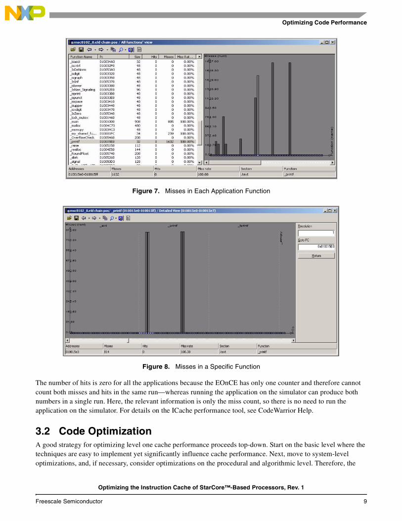
To examine the impact of instruction cache performance on an application and pinpoint the problematic functions, use the EOnCE, which can count ICache hits or misses. Figure 7 and Figure 8 are screen captures of the CodeWarrior® ICache performance tool, which uses the EOnCE to measure the number of hits/misses for each function. In Figure 7, the ICache tool gives detailed hit/miss information for each function of the application, which you can use to pinpoint the problematic locations in the code for cache performance optimization.
TAG
Valid Bits Line
TAG Index FetchSet# Address
31 03479 8
Way0; Index0
Way0; Index1
Way0; Index2
Way0; Index3
256 BytesOne per fetch set
10
Way1; Index0
Way1; Index1
Way1; Index2
Way1; Index3
Way15; Index0
Way15; Index1
Way15; Index2
Way15; Index3
Optimizing the Instruction Cache of StarCore™-Based Processors, Rev. 1
8 Freescale Semiconductor
Optimizing Code Performance
Figure 7. Misses in Each Application Function
Figure 8. Misses in a Specific Function
The number of hits is zero for all the applications because the EOnCE has only one counter and therefore cannot count both misses and hits in the same run—whereas running the application on the simulator can produce both numbers in a single run. Here, the relevant information is only the miss count, so there is no need to run the application on the simulator. For details on the ICache performance tool, see CodeWarrior Help.
3.2 Code OptimizationA good strategy for optimizing level one cache performance proceeds top-down. Start on the basic level where the techniques are easy to implement yet significantly influence cache performance. Next, move to system-level optimizations, and, if necessary, consider optimizations on the procedural and algorithmic level. Therefore, the
Optimizing the Instruction Cache of StarCore™-Based Processors, Rev. 1
Freescale Semiconductor 9
Optimizing Code Performance
structure of this section reflects the order in which to address the optimizations. At the most basic level, you need only activate the cache by setting the enable bit in the ICache control register and enabling the SC140 prefetch mechanism, as follows:
volatile unsigned short *pIFUR = (unsigned short *) 0x00f0ff60; volatile unsigned short *pWBCR = (unsigned short *) 0x00f0ff82; volatile unsigned short *pICCR = (unsigned short *) 0x00f0fc00;
int main(int argc, char *argv[]) {
*pIFUR = 0x0000; // Prefetch enabled. *pWBCR = 0x03FF; // Write Buffer enabled. *pICCR = 0xF001; // Cache enabled.
}
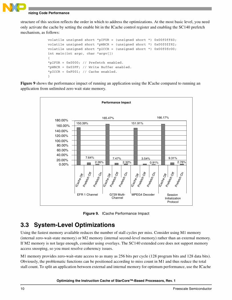
Figure 9 shows the performance impact of running an application using the ICache compared to running an application from unlimited zero wait state memory.
Figure 9. ICache Performance Impact
3.3 System-Level OptimizationsUsing the fastest memory available reduces the number of stall cycles per miss. Consider using M1 memory (internal zero-wait-state memory) or M2 memory (internal second-level memory) rather than an external memory. If M2 memory is not large enough, consider using overlays. The SC140 extended core does not support memory access snooping, so you must resolve coherency issues.
M1 memory provides zero-wait-state access to as many as 256 bits per cycle (128 program bits and 128 data bits). Obviously, the problematic functions can be positioned according to miss count in M1 and thus reduce the total stall count. To split an application between external and internal memory for optimum performance, use the ICache
180.00%
160.00%
140.00%120.00%
100.00%80.00%
0.00%
EFR 1 Channel G729 Multi-Channel
MPEG4 Decoder Session Initialization
Protocol
ICac
he O
ffP
refe
tch
Off
Pre
fetc
h O
nIC
ache
Off
Pre
fetc
h O
ffP
refe
tch
On
ICac
he O
ffP
refe
tch
Off
Pre
fetc
h O
n
ICac
he O
ffP
refe
tch
Off
Pre
fetc
h O
n
150.39%
7.64%
2.26%
165.47%
7.47%2.32%
151.91%
3.54%0.91%
166.17%
9.31%2.76%
Performance Impact
60.00%40.00%
20.00%
Optimizing the Instruction Cache of StarCore™-Based Processors, Rev. 1
10 Freescale Semiconductor
Optimizing Code Performance
performance tool shown in Figure 7 and Figure 8 to consider the misses each function produces. A useful guideline is to analyze the code size of the application and its miss rate and then maximize the “normalized miss rate,” defined as follows:
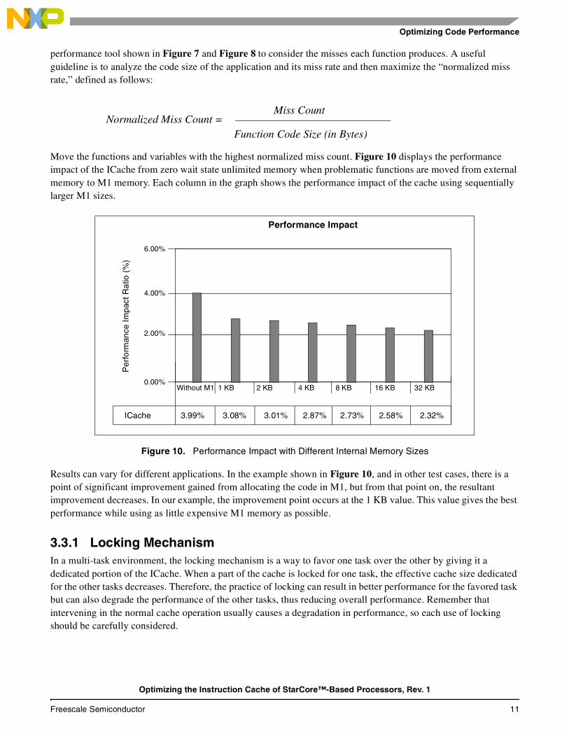
Move the functions and variables with the highest normalized miss count. Figure 10 displays the performance impact of the ICache from zero wait state unlimited memory when problematic functions are moved from external memory to M1 memory. Each column in the graph shows the performance impact of the cache using sequentially larger M1 sizes.
Figure 10. Performance Impact with Different Internal Memory Sizes
Results can vary for different applications. In the example shown in Figure 10, and in other test cases, there is a point of significant improvement gained from allocating the code in M1, but from that point on, the resultant improvement decreases. In our example, the improvement point occurs at the 1 KB value. This value gives the best performance while using as little expensive M1 memory as possible.
3.3.1 Locking MechanismIn a multi-task environment, the locking mechanism is a way to favor one task over the other by giving it a dedicated portion of the ICache. When a part of the cache is locked for one task, the effective cache size dedicated for the other tasks decreases. Therefore, the practice of locking can result in better performance for the favored task but can also degrade the performance of the other tasks, thus reducing overall performance. Remember that intervening in the normal cache operation usually causes a degradation in performance, so each use of locking should be carefully considered.
Normalized Miss Count = Miss Count
Function Code Size (in Bytes)
Performance Impact
Without M1 1 KB 2 KB 4 KB 8 KB 16 KB 32 KB
6.00%
4.00%
2.00%
0.00%
Per
form
ance
Impa
ct R
atio
(%
)
ICache 3.99% 3.08% 3.01% 2.87% 2.73% 2.58% 2.32%
Optimizing the Instruction Cache of StarCore™-Based Processors, Rev. 1
Freescale Semiconductor 11
Optimizing Code Performance
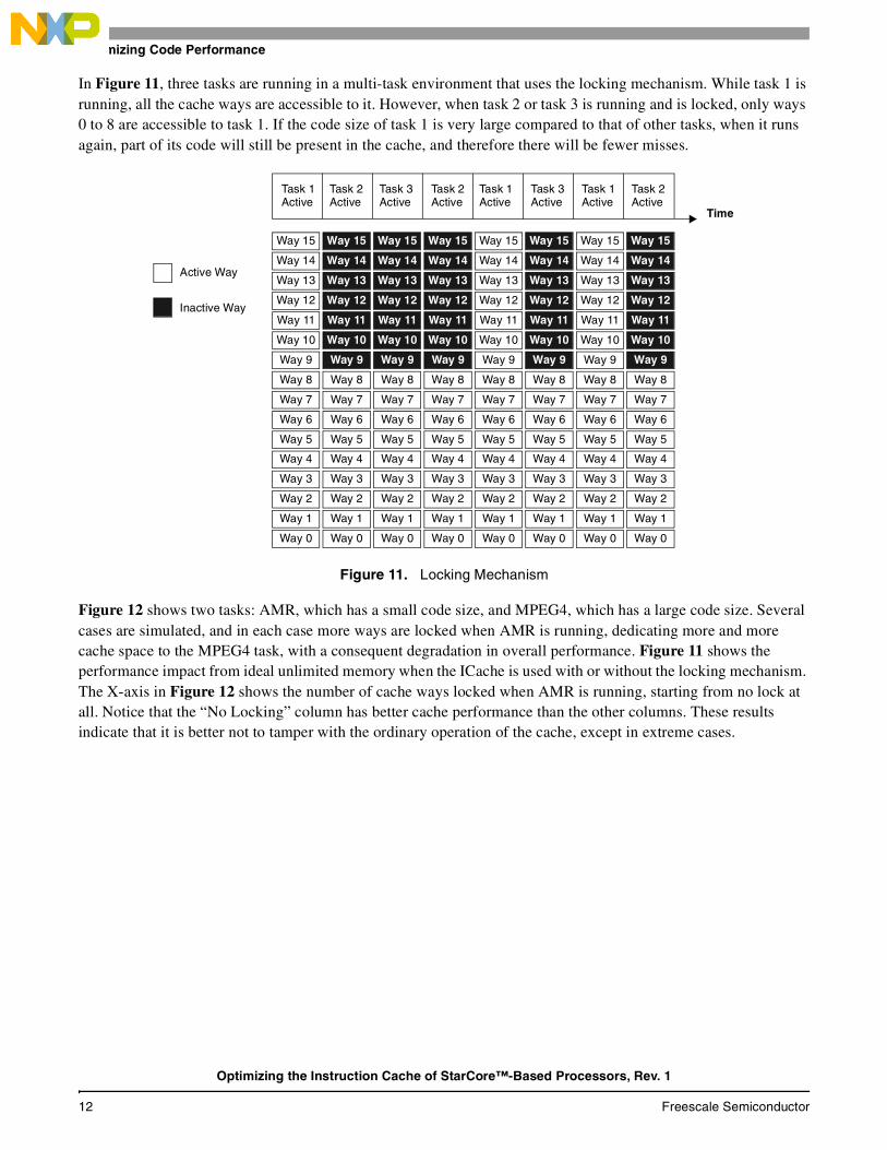
In Figure 11, three tasks are running in a multi-task environment that uses the locking mechanism. While task 1 is running, all the cache ways are accessible to it. However, when task 2 or task 3 is running and is locked, only ways 0 to 8 are accessible to task 1. If the code size of task 1 is very large compared to that of other tasks, when it runs again, part of its code will still be present in the cache, and therefore there will be fewer misses.
Figure 11. Locking Mechanism
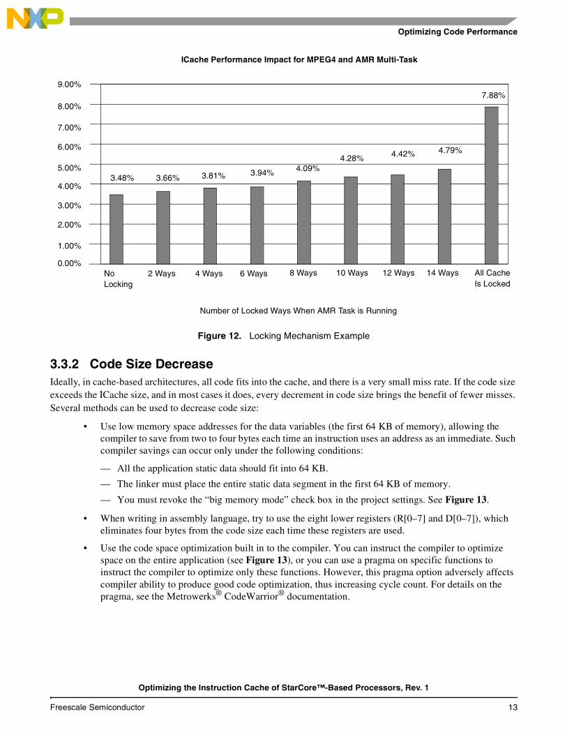
Figure 12 shows two tasks: AMR, which has a small code size, and MPEG4, which has a large code size. Several cases are simulated, and in each case more ways are locked when AMR is running, dedicating more and more cache space to the MPEG4 task, with a consequent degradation in overall performance. Figure 11 shows the performance impact from ideal unlimited memory when the ICache is used with or without the locking mechanism. The X-axis in Figure 12 shows the number of cache ways locked when AMR is running, starting from no lock at all. Notice that the “No Locking” column has better cache performance than the other columns. These results indicate that it is better not to tamper with the ordinary operation of the cache, except in extreme cases.
Way 9
Way 15
Way 14
Way 13
Way 12
Way 11
Way 10
Way 9
Way 15
Way 14
Way 13
Way 12
Way 10
Way 9
Way 15
Way 14
Way 13
Way 12
Way 11
Way 10
Way 9
Way 8
Way 7
Way 6
Way 5
Way 4
Way 3
Way 2
Way 1
Way 0
Way 11
Way 8
Way 7
Way 6
Way 5
Way 4
Way 3
Way 2
Way 1
Way 0
Way 8
Way 7
Way 6
Way 5
Way 4
Way 3
Way 2
Way 1
Way 0
Way 15
Way 14
Way 13
Way 12
Way 11
Way 10
Way 8
Way 7
Way 6
Way 5
Way 4
Way 3
Way 2
Way 1
Way 0
Way 15
Way 14
Way 13
Way 12
Way 11
Way 10
Way 9
Way 8
Way 7
Way 6
Way 5
Way 4
Way 3
Way 2
Way 1
Way 0
Way 15
Way 14
Way 13
Way 12
Way 11
Way 10
Way 9
Way 8
Way 7
Way 6
Way 5
Way 4
Way 3
Way 2
Way 1
Way 0
Way 15
Way 14
Way 13
Way 12
Way 11
Way 10
Way 9
Way 8
Way 7
Way 6
Way 5
Way 4
Way 3
Way 2
Way 1
Way 0
Way 15
Way 14
Way 13
Way 12
Way 11
Way 10
Way 9
Way 8
Way 7
Way 6
Way 5
Way 4
Way 3
Way 2
Way 1
Way 0
Task 1Active
Task 2Active
Task 3Active
Task 2Active
Task 1Active
Task 3Active
Task 1Active
Task 2Active
Active Way
Inactive Way
Time
Optimizing the Instruction Cache of StarCore™-Based Processors, Rev. 1
12 Freescale Semiconductor
Optimizing Code Performance
Figure 12. Locking Mechanism Example
3.3.2 Code Size DecreaseIdeally, in cache-based architectures, all code fits into the cache, and there is a very small miss rate. If the code size exceeds the ICache size, and in most cases it does, every decrement in code size brings the benefit of fewer misses. Several methods can be used to decrease code size:
• Use low memory space addresses for the data variables (the first 64 KB of memory), allowing the compiler to save from two to four bytes each time an instruction uses an address as an immediate. Such compiler savings can occur only under the following conditions:
— All the application static data should fit into 64 KB.
— The linker must place the entire static data segment in the first 64 KB of memory.
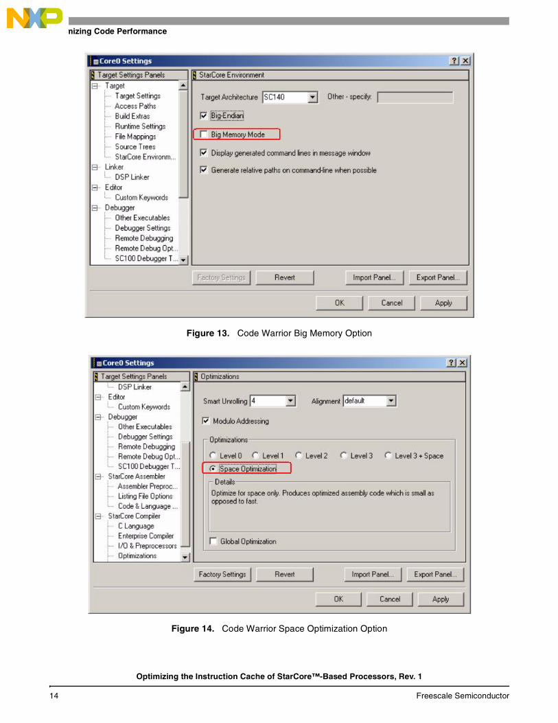
— You must revoke the “big memory mode” check box in the project settings. See Figure 13.
• When writing in assembly language, try to use the eight lower registers (R[0–7] and D[0–7]), which eliminates four bytes from the code size each time these registers are used.
• Use the code space optimization built in to the compiler. You can instruct the compiler to optimize space on the entire application (see Figure 13), or you can use a pragma on specific functions to instruct the compiler to optimize only these functions. However, this pragma option adversely affects compiler ability to produce good code optimization, thus increasing cycle count. For details on the pragma, see the Metrowerks® CodeWarrior® documentation.
9.00%
8.00%
7.00%
6.00%
5.00%
4.00%
0.00%
3.00%
2.00%
1.00%
ICache Performance Impact for MPEG4 and AMR Multi-Task
Number of Locked Ways When AMR Task is Running
3.48% 3.66% 3.81% 3.94% 4.09%4.28% 4.42% 4.79%
7.88%
No Locking
2 Ways 4 Ways 6 Ways 8 Ways 10 Ways 12 Ways 14 Ways All CacheIs Locked
Optimizing the Instruction Cache of StarCore™-Based Processors, Rev. 1
Freescale Semiconductor 13
Optimizing Code Performance
Figure 13. Code Warrior Big Memory Option
Figure 14. Code Warrior Space Optimization Option
Optimizing the Instruction Cache of StarCore™-Based Processors, Rev. 1
14 Freescale Semiconductor

Optimizing Code Performance
3.4 Procedural-Level OptimizationsThe procedural-level optimizations discussed in this section are function alignment and function inlining.
3.4.1 Function Alignment A miss is served by the instruction fetch unit (IFU). After the missed address is fetched into the ICache, the IFU continues to fetch the sequential instruction fetch-sets until one of the following events occurs:
• End of the cache line
• A different ICache miss
• A transaction with higher-priority bus use
Most misses occur at the beginning of a cache line, so even if program flow is sequential (no branches) there can still be misses in the ICache. Aligning a function with the beginning address of a cache line decreases the total number of cache lines in which the function occurs, thereby reducing the miss count. In Figure 15, the function occupies one cache line less after the alignment.
Figure 15. Function Alignment
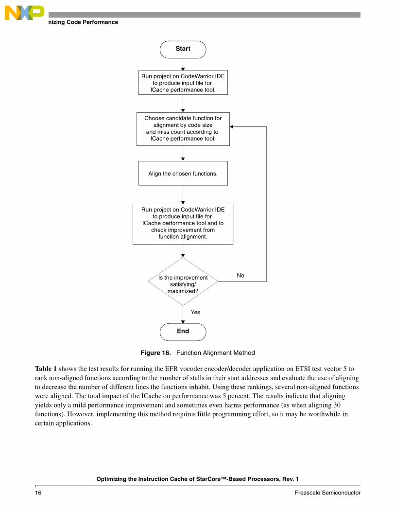
However, function alignment increases code size because empty spaces are created, thus counteracting the benefits of aligning the functions and sometimes can even degrading application performance. Figure 16 shows a flow chart of the iterative method needed to archive the best results.
Assembly functions are aligned by adding the phrase .align 256 at the start of each function to be aligned. The following example shows the way to align a C code function using the pragma directive supported in Code Warrior 2.5.
void foo() {
#pragma align foo 256 printf("Hello!\n");
}
Without Alignment With Alignment of 256
Function Start Function Start
Function End Function End
Optimizing the Instruction Cache of StarCore™-Based Processors, Rev. 1
Freescale Semiconductor 15
Optimizing Code Performance
Figure 16. Function Alignment Method
Table 1 shows the test results for running the EFR vocoder encoder/decoder application on ETSI test vector 5 to rank non-aligned functions according to the number of stalls in their start addresses and evaluate the use of aligning to decrease the number of different lines the functions inhabit. Using these rankings, several non-aligned functions were aligned. The total impact of the ICache on performance was 5 percent. The results indicate that aligning yields only a mild performance improvement and sometimes even harms performance (as when aligning 30 functions). However, implementing this method requires little programming effort, so it may be worthwhile in certain applications.
Start
Run project on CodeWarrior IDEto produce input file for
ICache performance tool.
Choose candidate function foralignment by code size
and miss count according to ICache performance tool.
Align the chosen functions.
Run project on CodeWarrior IDEto produce input file for
ICache performance tool and tocheck improvement from
function alignment.
Is the improvementsatisfying/
maximized?
End
Yes
No
Optimizing the Instruction Cache of StarCore™-Based Processors, Rev. 1
16 Freescale Semiconductor

Optimizing Code Performance
3.4.2 Function Inlining When there is a change of flow, such as BRA and JSR, and the called function/code section is not in the cache, a miss occurs. To minimize the number of misses, function inlining is performed. When a function is inlined, its code is prefetched with the caller function code so that misses at the start of the called function are reduced.
Figure 17. Function Inlining
However, if the inlined function is called from many different places and is inlined in all these places, the code size increases, counteracting the benefit of inlining. It is advisable to inline only functions with the following properties:
• They are called from very few places (up to three places).
• Their code size is very small.
• They get more stalls at their starting addresses than other candidate functions.
The EFR vocoder application ran a test script to rank functions according to the number of stalls occurring in their start addresses. The function code size and number of times called were also considered in order to minimize the change in code size. Table 18 shows a flow chart of the iterative method used to achieve the best results.
Table 1. Function Aligning
Test Number
DescriptionTotal
Program Miss Count
Total Program
Stall Count
Stall Count Improvement
Code Size(Bytes)
Code Size Increase (Bytes)
1 No alignment 6084 78187 0 67536 0
2 Alignment of 5 functions
6065 76554 2% 67690 154
3 Alignment of 16 functions
5901 75634 3.3% 68096 560
4 Alignment of 30 functions
6159 79944 –2.2% 69306 1808
Cache Miss
Cache Miss
No Cache Miss
Without Inline, A Cache Miss
With Inline, No Cache Miss
Optimizing the Instruction Cache of StarCore™-Based Processors, Rev. 1
Freescale Semiconductor 17

Optimizing Code Performance
Figure 18. Function Inlining Method
A function can be inlined only when global optimization is applied to a library from CodeWarrior or when the inlined function implementation is the same file as the caller function. A pragma placed in the caller function before the function call instructs the compiler to inline the function in that specific function call. This option allows you to inline the functions only for code that executes a great many times, such as inside loops, to increase function inlining efficiency. The pragma can also be used immediately after the statement where function_name is called. If this statement contains several calls to function_name, they are all inlined. If only certain calls should be inlined, set a pragma noinline in the function to be called (as shown in Example 1). Otherwise, an automatic inline might interfere with it so that the designated call is inlined but other calls where inlining is not desired are inlined as well.
Start
Run project on CodeWarrior IDEto produce input file for
ICache performance tool.
Choose candidate functions forinlining by code size, number ofcalls, and miss count according
to ICache performance tool.
Inline the chosen functions.
Run project on CodeWarrior IDEto produce input file for
ICache performance tool and tocheck improvement from
function inlining.
Is the improvementsatisfying/
maximized?
End
Yes
No
Optimizing the Instruction Cache of StarCore™-Based Processors, Rev. 1
18 Freescale Semiconductor

Optimizing Code Performance
Example 1. Pragma noinline
int foo1(int x, int y){
#pragma noinline return (x+y);
} int foo2(int X, int Y)
{ int Acc; Acc = foo1(X, Y); // This one is not inlined Acc = Acc + foo1(X, Y);// This one is inlined #pragma inline_call foo1 Acc = Acc + foo1(X, Y);// This one is not inlined return Acc;
}
Table 2 presents the test results of running the EFR encoder/decoder application on test vector 5. These results show that inlining yields only a small improvement in performance. Implementing this method requires little programming effort, so it may be worthwhile in certain applications.
Note: If both inlining and alignment are performed, inlining should implemented first because inlining yields better results, and each method influences the results of the other. In both cases, (alignment and inlining), the changes can sometimes harm application performance, so each change should be examined.
3.5 Algorithmic-Level OptimizationsThis section discusses how to avoid ICache capacity misses and conflict misses.
3.5.1 Instruction Cache Capacity MissesIf the ICache is not big enough to hold all the functions of a loop, the loop may need to be split up to achieve code reuse without evictions. Splitting the loop may increase the memory requirements for temporary buffers to hold output data. Assume that the combined code size of function_1 and function_2, as shown in Example 2, is larger than the size of the ICache. The code loop has been split to allow both functions to execute from the ICache repeatedly, considerably reducing misses. However, the temporary buffer tmp[] now has to hold all intermediate results from each call to function_1.
Table 2. Function Inlining
Test Number
DescriptionTotal Program
Miss Count
Total Program
Stall Count
Stall Count Improvement
Code Size(Bytes)
Code Size Increase (Bytes)
1 No inlining 6084 78187 67536
2 Inlining of 6 functions
5800 74550 4.5% 67696 198
Optimizing the Instruction Cache of StarCore™-Based Processors, Rev. 1
Freescale Semiconductor 19
Optimizing Code Performance
Example 2. Combined Code Size is Larger than ICache
for (i=0; i<N; i++) {
function_1(in[i], tmp); function_2(tmp, out[i]);
}
Example 3. Code Split to Execute from ICache
for (i=0; i<N; i++) {
function_1(in[i], tmp[i]); } for (i=0; i<N; i++) {
function_2(tmp[i], out[i]);}
These examples are used in a multi-channel GSM EFR vocoder encoder/decoder application. There are two projects. The first executes the whole frame (encode and decode) and then switches to the next channel. In the second project, the encoder and decoder are broken into five subprocesses, each called sequentially, to process the entire frame. Every frame of an N channel EFR vocoder is processed in the following order:
{ Decoder (sub-process 1) * N channels. Encoder (sub-process 1) * N channels. Encoder (sub-process 2) * N channels. Decoder (sub-process 2) * N channels. Encoder (sub-process 3) * N channels. Decoder (sub-process 3) * N channels. Encoder (sub-process 4) * N channels. Decoder (sub-process 4) * N channels.
}
These two projects prevent many ICache capacity and conflict misses. Simulations of these projects were run on an 8-channel EFR vocoder encoder/decoder. Using the sub-frame encode/decode method reduced the total miss counts by 30 percent. In addition, the miss ratio was comparable to the miss ratio using the whole frame encode/decode method.
3.5.2 Instruction Cache Conflict MissesThe SC140 instruction cache is a highly associative cache (16 ways), so the miss scenario described in this section has a very low probability of occurrence. All code of the working set fits into the cache so that there are no capacity misses by definition, but conflict misses occur. This section first explains how instruction cache conflict misses are caused and then describes how allocating the code contiguously in memory can eliminate the conflict misses.
On the SC140 extended core, 17 different memory addresses are mapped to the same line so that the seventeenth memory access evicts the first one. The chances that this will actually occur are very small. However, if the cache was direct mapped, only two memory addresses mapped to the same line are sufficient to cause eviction. Direct-mapped caches have a much higher conflict miss rate than a 16-way set associative cache.
The compiler and linker do not consider cache conflicts, and an inappropriate memory layout may cause conflict misses during execution. Most evictions can be avoided by altering the order in which functions are linked in memory; that is, by allocating code that is accessed within some local time window contiguously in memory.
Optimizing the Instruction Cache of StarCore™-Based Processors, Rev. 1
20 Freescale Semiconductor
Conclusions
Consider the code in Example 4. Assume that the linker has placed function_1 to function_17 so that they overlap in the instruction cache. When function_1 to function_16 are called the first time, they are allocated in the ICache, causing misses. A following call to function_17 causes its code to be allocated in the ICache and to evict parts of the code of function_1, since these lines overlap. When function_1 is called again in the next iteration, its lines must be brought back into instruction cache, only to be evicted again by function_2. Function_2 is then evicted by function_3 and so forth. For all following iterations, each time the functions evict one another and thereby cause cache misses. These are conflict misses. They can be completely avoided by allocating the code of any two functions from the 17 functions into non-conflicting sets. The most straightforward way is to place the code of the two functions contiguously in memory.
It also would be possible to move function_17 to a place where none of its sets conflicts with the other functions. Although this would prevent eviction, the first method has the advantage that you need not worry about absolute address placement and can simply change the order in which the functions are allocated in memory.
Example 4. Instruction Cache Conflict
for (i=0; i<N; i++) {
function_1(); function_2(); . . . function_16(); function_17();
}
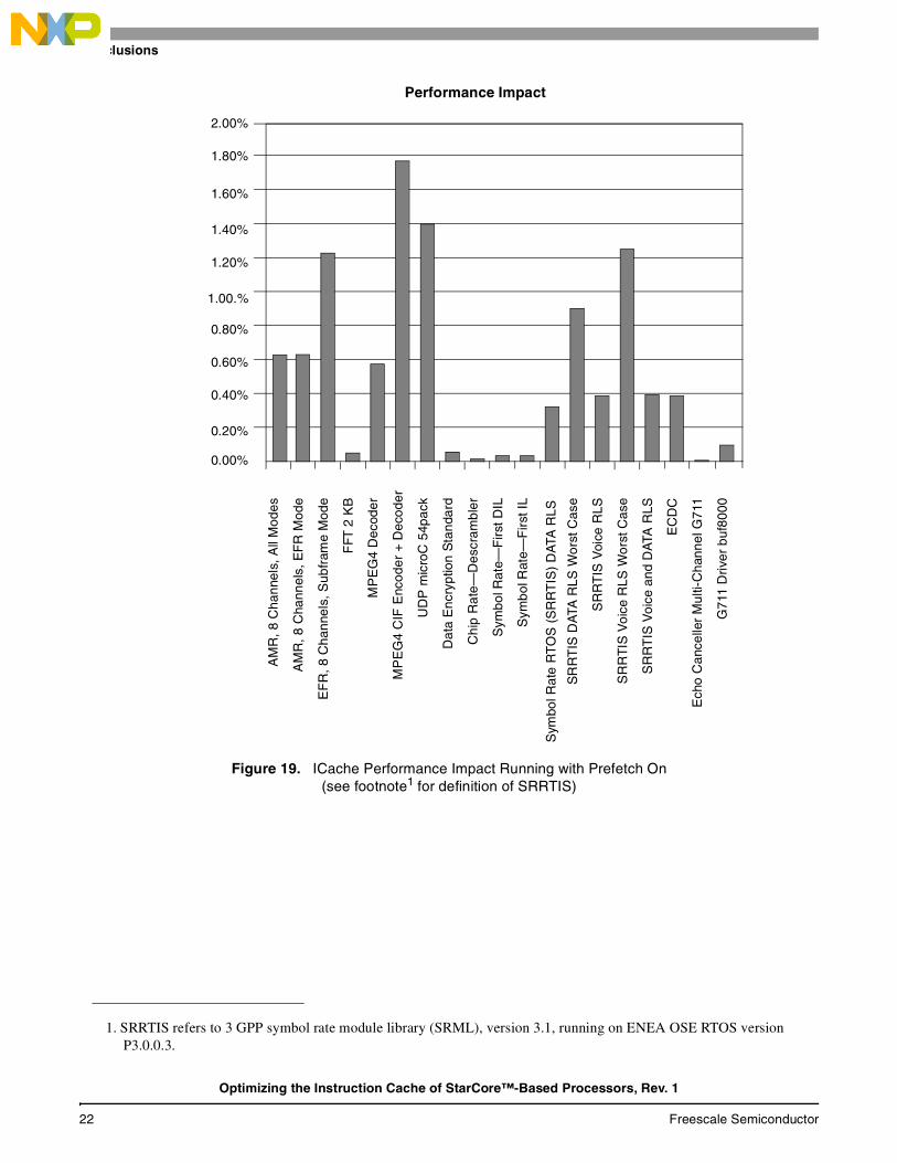
4 Conclusions The performance impact of the ICache was measured on many applications. Figure 19 shows the performance impact of running an application using the ICache compared to running the application from unlimited zero wait state memory. The complete application was simulated in a multi-core environment. Each application executed simultaneously on all the four cores of the SC140 extended core. A shift was added to each core to make the cores nonsynchronous so one core would not cause the other cores always to get hit on the ICache. The research results make it very clear that use of the ICache has almost no impact on an application’s performance. These results strongly indicate that in most cases there is no need for cache optimizations.
Because of its high associativity level (16 way set associative) and powerful prefetch mechanism, the SC140 extended core has a high cache rate and requires almost no optimization. However, small changes that can be easily implemented—such as enabling prefetch—may result in massive improvements in application performance. It is good programming practice to be aware of ICache impact on application performance and so direct a design to be “cache-friendly”.
Optimizing the Instruction Cache of StarCore™-Based Processors, Rev. 1
Freescale Semiconductor 21
Conclusions
Figure 19. ICache Performance Impact Running with Prefetch On(see footnote1 for definition of SRRTIS)
1. SRRTIS refers to 3 GPP symbol rate module library (SRML), version 3.1, running on ENEA OSE RTOS version P3.0.0.3.
1.80%
1.60%
1.40%
1.20%
1.00.%
0.80%
0.00%
0.60%
0.40%
0.20%
2.00%
Performance Impact
AM
R, 8
Cha
nnel
s, A
ll M
odes
AM
R, 8
Cha
nnel
s, E
FR
Mod
e
MP
EG
4 D
ecod
er
EF
R, 8
Cha
nnel
s, S
ubfr
ame
Mod
e
FFT
2 K
B
MP
EG
4 C
IF E
ncod
er +
Dec
oder
G71
1 D
river
buf
8000
UD
P m
icro
C 5
4pac
k
Chi
p R
ate—
Des
cram
bler
Sym
bol R
ate
RT
OS
(S
RR
TIS
) D
ATA
RLS
Dat
a E
ncry
ptio
n S
tand
ard
Sym
bol R
ate—
Firs
t DIL
Sym
bol R
ate—
Firs
t IL
SR
RT
IS D
ATA
RLS
Wor
st C
ase
SR
RT
IS V
oice
RLS
SR
RT
IS V
oice
RLS
Wor
st C
ase
SR
RT
IS V
oice
and
DA
TA R
LS
EC
DC
Ech
o C
ance
ller
Mul
ti-C
hann
el G
711
Optimizing the Instruction Cache of StarCore™-Based Processors, Rev. 1
22 Freescale Semiconductor
References
5 ReferencesIn addition to the reference manual for your StarCore-based DSP device, you should also consult the following documents, all of which are available through the web site listed on the back cover of this document:
[1] CodeWarrior Development Tools: Metrowerks Enterprise C Compiler User’s Manual (available on the Metrowerks web site, which is accessible under “Related Links” at the web site listed on the back cover of this document. On the Metrowerks web site, the manual is available in the Developer Resources section under the “Support” tab.
[2] CodeWarrior Development Tools for StarCore DSP: Targeting Manual. Also available on the Metrowerks web site.
[3] SC140 DSP Core Reference Manual (MNSC140CORE/D)
Optimizing the Instruction Cache of StarCore™-Based Processors, Rev. 1
Freescale Semiconductor 23
AN2714
Information in this document is provided solely to enable system and software implementers to use Freescale Semiconductor products. There are no express or implied copyright licenses granted hereunder to design or fabricate any integrated circuits or integrated circuits based on the information in this document.
Freescale Semiconductor reserves the right to make changes without further notice to any products herein. Freescale Semiconductor makes no warranty, representation or guarantee regarding the suitability of its products for any particular purpose, nor does Freescale Semiconductor assume any liability arising out of the application or use of any product or circuit, and specifically disclaims any and all liability, including without limitation consequential or incidental damages. “Typical” parameters which may be provided in Freescale Semiconductor data sheets and/or specifications can and do vary in different applications and actual performance may vary over time. All operating parameters, including “Typicals” must be validated for each customer application by customer’s technical experts. Freescale Semiconductor does not convey any license under its patent rights nor the rights of others. Freescale Semiconductor products are not designed, intended, or authorized for use as components in systems intended for surgical implant into the body, or other applications intended to support or sustain life, or for any other application in which the failure of the Freescale Semiconductor product could create a situation where personal injury or death may occur. Should Buyer purchase or use Freescale Semiconductor products for any such unintended or unauthorized application, Buyer shall indemnify and hold Freescale Semiconductor and its officers, employees, subsidiaries, affiliates, and distributors harmless against all claims, costs, damages, and expenses, and reasonable attorney fees arising out of, directly or indirectly, any claim of personal injury or death associated with such unintended or unauthorized use, even if such claim alleges that Freescale Semiconductor was negligent regarding the design or manufacture of the part.
Freescale™ and the Freescale logo are trademarks of Freescale Semiconductor, Inc. StarCore is a trademark of StarCore LLC. All other product or service names are the property of their respective owners.
© Freescale Semiconductor, Inc. 2004.
How to Reach Us:Home Page:www.freescale.com
E-mail:[email protected]
USA/Europe or Locations not listed:Freescale Semiconductor Technical Information Center, CH3701300 N. Alma School RoadChandler, Arizona 85224+1-800-521-6274 or [email protected]
Europe, Middle East, and Africa:Freescale Halbleiter Deutschland GMBHTechnical Information CenterSchatzbogen 781829 München, Germany+44 1296 380 456 (English)+46 8 52200080 (English)+49 89 92103 559 (German)+33 1 69 35 48 48 (French)[email protected]
Japan:Freescale Semiconductor Japan Ltd. HeadquartersARCO Tower 15F1-8-1, Shimo-Meguro, Meguro-ku,Tokyo 153-0064, Japan0120 191014 or +81 3 5437 [email protected]
Asia/Pacific:Freescale Semiconductor Hong Kong Ltd.Technical Information Center2 Dai King StreetTai Po Industrial EstateTai Po, N.T. Hong Kong+800 2666 8080
For Literature Requests Only:Freescale Semiconductor Literature Distribution CenterP.O. Box 5405Denver, Colorado 802171-800-441-2447 or 303-675-2140Fax: [email protected]
Rev. 111/2004