an1980 application noteapplication-notes.digchip.com/005/5-10295.pdf · · 2009-02-08the list of...
TRANSCRIPT

AN1980/0704 1/22
Rev. 1
1 - INTRODUCTION
The Super10 core is the most recent member of the ST10 family with a wide addressing space. A fractionof the Super10 16 Mbyte addressable space is covered by dedicated buses for on-chip peripherals,on-chip program and data memories. The External Bus Controller allows access to additional memoriesand peripherals. The external bus supports various configurations to address several memories andperipherals in parallel, therefore it can be tailored to fit perfectly into a given application system. The pur-pose of this note is to give pieces of advice on how to program EBC registers to obtain the best possibleperformance.
AN1980APPLICATION NOTE
Programming Super10 External Bus Controller Registers
AN1980 APPLICATION NOTE
2/22
1 - INTRODUCTION ........................................................................................................ 1
2 - EXTERNAL BUS CONTROLLER (EBC) ................................................................... 3
2.1 - OVERVIEW ................................................................................................................ 3
2.2 - TIMING PRINCIPLES ................................................................................................. 4
3 - R303 EVALUATION BOARD BUS EXCHANGES VIA EBC .................................... 5
3.1 - THEORETICAL ANALYSIS ........................................................................................ 5
3.1.1 - Super10 R303 Timings and Waveforms ..................................................................... 63.1.2 - Comparison with uPD434008AL SRAM Timings ....................................................... 83.1.3 - Comparison With M29W200BT Flash Timings ......................................................... 113.1.4 - Numerical Application ................................................................................................. 14
4 - PRACTICAL APPROACH ......................................................................................... 15
4.1 - BOARD ACTIVATION ................................................................................................ 15
4.2 - HOW TO SET-UP EBC REGISTERS ........................................................................ 15
5 - TIMING VALIDATION ................................................................................................ 16
5.1 - METHODOLOGY ....................................................................................................... 16
5.2 - RESULTS ................................................................................................................... 16
6 - CONCLUSION ........................................................................................................... 17
7 - REFERENCES ........................................................................................................... 17
8 - APPENDIX ................................................................................................................. 18
8.1 - EBC REGISTERS INITIALIZATION EXAMPLE - FCPU = 133MHZ .......................... 18
8.2 - VALIDATION TEST PROGRAM .......................................................................... 19
TABLE OF CONTENTS
AN1980 APPLICATION NOTE
3/22
2 - EXTERNAL BUS CONTROLLER (EBC)
2.1 - Overview
The integrated External Bus Controller (EBC) is configured thanks to a set of registers. The control regis-ters bring enough flexibility in the bus timings and accuracy in the addressing of external memories andperipherals to adapt the Super10 to almost all applications.
The list of control registers is given in Table 1 on page 3 and the registers are explained in the followingsections.
Notes: 1. Depends on reset bus configuration (latched in the RSTCFG register).2. Refer to the product specification for the exact value.
The EBC supports up to 8 external chip select channels (CS0..CS7). Each of these chip select signal isprogrammable via a set of registers. The FCONCSx registers specify the external bus cycles in terms ofaddress (multiplexed or demultiplexed), data width (16-bit or 8-bit wide), chip select enable and READYsignal control.
The timing of the bus access is controlled by the TCONCSx timing configuration registers, which specifythe length of the different access phases. All the parameters used to access within a specific addressarea are defined via the corresponding ADDRSELx address select register.
The seven register sets FCONCS1/TCONCS1/ADDRSEL1...FCONCS7/TCONCS7/ADDRSEL7 allow todefine seven independent "address windows" with their specific parameters, while all external accessesoutside these windows are controlled via FCONCS0 and TCONCS0 registers.
The external bus timing is related to the CPU clock. All bus signals are generated in relation to the risingedge of this clock. This last affirmation will help the reader to fully understand the further timing wave-forms.
Table 1: EBC Configuration Registers Overview
Name CS Description Reset Value
EBCMOD0 All Global configuration of EBC pins 0XXXh 1
TCONCS0 0 Timing control for CS0 7A7Fh 2
FCONCS0 0 Function control for CS0 00X1h 1
TCONCS1-7 1-7 Timing control for for CS1...CS7 0000h
FCONCS1-7 1-7 Function control for for CS1...CS7 0000h
ADDRSEL1-7 1-7 Address window selection for CS1...CS7 0000h

AN1980 APPLICATION NOTE
4/22
2.2 - Timing Principles
The timing of the external bus accesses can be adapted to demultiplexed or multiplexed buses. Oneaccess cycle is split in six phases. Some phases are more related to one of the access types (demulti-plexed or multiplexed). The following description focuses on demultiplexed memory accesses *.
* The difference between a multiplexed and demultiplexed access is that in the former only one bus isused to vehicle sequentialy the address and data, instead of two dedicated buses in the later.
– A Phase - 0 to 3 clock periods - TSCONCSx.PHAx bit-field value.
The A phase cycles (data bus drivers are forced to tri-state) are only inserted when the current accessis not using the same Chip Select line (CS) than the previous one.
– B Phase - 1 or 2 clock periods long - TCONCSx.PHBx bit-field value + 1.
It defines the minimal possible ALE active length (1 clock period). During this phase, the address bus isvalid for the external device.
– C Phase - 0 to 3 clock periods - TCONCSx.PHCx bit-field value.
C phase cycles can be used to delay the read/write command signals.
– D Phase - 0 or 1 clock period - TCONCSx.PHDx bit field value.
In write mode, it participates to the set-up time of the data bus before the write command becomes ac-tive.
– E Phase - 1 to 32 clock periods long - TCONCSx.PHEx bit field value + 1.
It determines the read/write signal duration and number of wait-states being inserted.
– F Phase - 0 to 3 clock periods - TCONCSx.PHFx bit-field value.
Addresses and write data are held while the write command is inactive. The number of hold-states beinginserted at the F phase is independently programmed by TCONCSx.RDPHFx for read accesses andTCONCSx.WRPHFx for write accesses. In write mode, it offers a way to adjust the hold time of the databus.
Refer to [1] for more details.
AN1980 APPLICATION NOTE
5/22
3 - R303 EVALUATION BOARD BUS EXCHANGES VIA EBC
3.1 - Theoretical Analysis
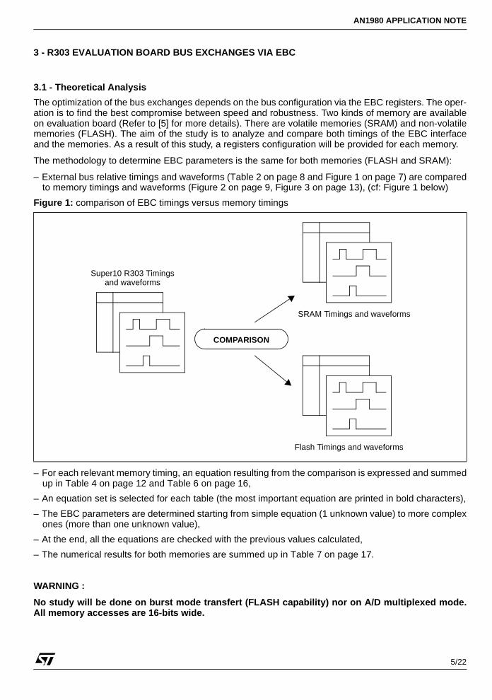
The optimization of the bus exchanges depends on the bus configuration via the EBC registers. The oper-ation is to find the best compromise between speed and robustness. Two kinds of memory are availableon evaluation board (Refer to [5] for more details). There are volatile memories (SRAM) and non-volatilememories (FLASH). The aim of the study is to analyze and compare both timings of the EBC interfaceand the memories. As a result of this study, a registers configuration will be provided for each memory.
The methodology to determine EBC parameters is the same for both memories (FLASH and SRAM):
– External bus relative timings and waveforms (Table 2 on page 8 and Figure 1 on page 7) are comparedto memory timings and waveforms (Figure 2 on page 9, Figure 3 on page 13), (cf: Figure 1 below)
– For each relevant memory timing, an equation resulting from the comparison is expressed and summedup in Table 4 on page 12 and Table 6 on page 16,
– An equation set is selected for each table (the most important equation are printed in bold characters),
– The EBC parameters are determined starting from simple equation (1 unknown value) to more complexones (more than one unknown value),
– At the end, all the equations are checked with the previous values calculated,
– The numerical results for both memories are summed up in Table 7 on page 17.
WARNING :
No study will be done on burst mode transfert (FLASH capability) nor on A/D multiplexed mode.All memory accesses are 16-bits wide.
Figure 1: comparison of EBC timings versus memory timings
Super10 R303 Timings
SRAM Timings and waveforms
Flash Timings and waveforms
COMPARISON
and waveforms

AN1980 APPLICATION NOTE
6/22
3.1.1 - Super10 R303 Timings and Waveforms
Figure 2: External Bus Relative Timing Waveforms, Demultiplexed Mode
TA TC TETD TFTB
A23:A0
Data in
Data out
CS7:CS0
RD
AD15:AD0
WR
Rea
d cy
cle
Writ
e cy
cle
t12
t28
t41
t84
t20t14
t18
t22t24
t80
t17

AN1980 APPLICATION NOTE
7/22
Table 2: External Bus Relative Timings, Demultiplexed Mode
Notes: 1. Max worst case spec, one wait state is needed (Te = 15ns@Fcpu = 133MHz).
2. The hold time can be set to 0ns (Internal and output clocks are delayed resulting in a negative value at timing analysis).
Timing Description Symbol Minimum Maximum Unit
(A23:A0) / BHE / (CS7:CS0) set-up time to RD / WR / WRL / WRH falling edge
t80 Ta + Tc + Td + (Tb - 1.37)
ns
RD / WR / WRL / WRH low time t12 Te - 0.78 ns
RD falling edge to valid data (AD15:AD0) in t14 Te - 10.17 1) ns
Address (A23:A0)/BHE / (CS7:CS0) to valid data (AD15:AD0) in t17 Ta + Tb + Tc + Td + Te - 11.42
ns
Data (AD15:AD0) hold time after RD rising edge t18 -1.45 2) ns
Data (AD15:AD0) tristate time after RD rising edge t20 Tf - 1.56 ns
Data (AD15:AD0) tristate time after (CS7:CS0) rising edge t84 1.06 ns
Data (AD15:AD0) out setup time to WR / WRL / WRH rising edge t22 Td + (Te- 2.72) ns
Valid Data (AD15:AD0) out hold time after WR / WRL / WRH rising edge
t24 Tf + 0.77 ns
Address (A23:A0) / BHE hold after RD / WR / WRL / WRH rising edge
t28 Tf + 0.17 ns
Chip Select (CS7:CS0) hold after RD / WR / WRL / WRH rising edge
t41 Tf + 0.35 ns
AN1980 APPLICATION NOTE
8/22
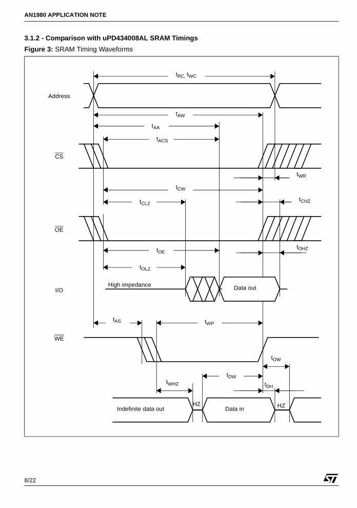
3.1.2 - Comparison with uPD434008AL SRAM Timings
Figure 3: SRAM Timing Waveforms
Address
Data out
Data in
CS
OE
I/O
WE
High impedance
HZHZIndefinite data out
tAA
tACS
tCLZ
tOE
tOLZ
tOHZ
tCHZ
tOW
tDH
tDWtWHZ
tWPtAS
tWR
tAW
tCW
tRC, tWC
AN1980 APPLICATION NOTE
9/22
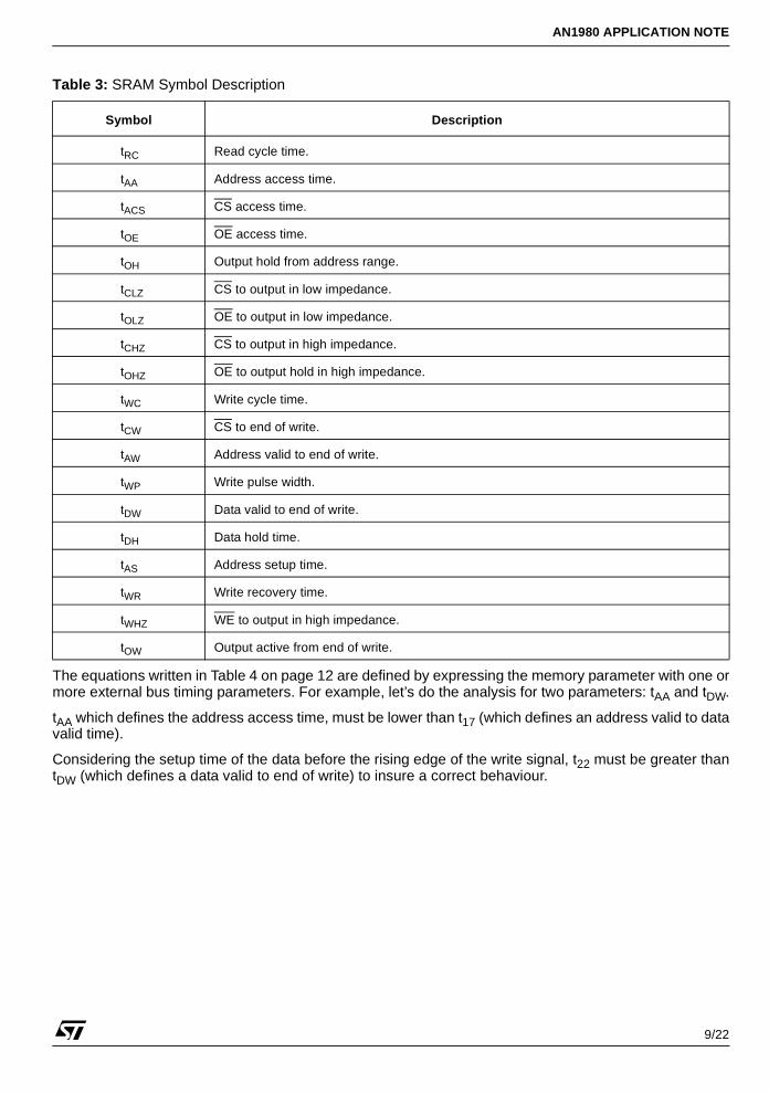
Table 3: SRAM Symbol Description
The equations written in Table 4 on page 12 are defined by expressing the memory parameter with one ormore external bus timing parameters. For example, let’s do the analysis for two parameters: tAA and tDW.
tAA which defines the address access time, must be lower than t17 (which defines an address valid to datavalid time).
Considering the setup time of the data before the rising edge of the write signal, t22 must be greater thantDW (which defines a data valid to end of write) to insure a correct behaviour.
Symbol Description
tRC Read cycle time.
tAA Address access time.
tACS CS access time.
tOE OE access time.
tOH Output hold from address range.
tCLZ CS to output in low impedance.
tOLZ OE to output in low impedance.
tCHZ CS to output in high impedance.
tOHZ OE to output hold in high impedance.
tWC Write cycle time.
tCW CS to end of write.
tAW Address valid to end of write.
tWP Write pulse width.
tDW Data valid to end of write.
tDH Data hold time.
tAS Address setup time.
tWR Write recovery time.
tWHZ WE to output in high impedance.
tOW Output active from end of write.

AN1980 APPLICATION NOTE
10/22
Table 4: SRAM Timings Versus EBC Timings
Notes: 1. Address and chip select bits toggle at the same time.
2. Useful in case of address controlled access (CS = OE = VIL) instead of CS controlled access.
3. Useless since WR and RD signals cannot be active at the same time.
Remark : Refer to [2] for more details on the memory product.
No Symbol Min (ns) Max (ns) Equation Result (ns) Notes
SR
AM
RE
AD
CY
CL
E
1 tRC 15 t80+t12+t28 > tRC Tabcdef > 16.98
2 tAA 15 t17 > tAA Tabcde > 26.42
3 tACS 15 idem idem 1
4 tOE 7 t14 > tOE Te > 17.17
5 tOH 3 Not Applicable Not Applicable 2
6 tCLZ 3 t80 > tCLZ Tabcd > 4.37
7 tOLZ 0 t14 > tOLZ Te > 10.17
8 tCHZ 7 t84 > tCHZ Tf > 5.94
9 tOHZ 7 t20 > tOHZ Tf > 5.44
SR
AM
WR
ITE
CY
CL
E
10 tWC 15 t80+t12+t28 > tWC Tabcdef > 16.98
11 tCW 10 t80+t12 > tCW Tabcde > 12.15
12 tAW 10 idem idem 1
13 tWP 10 t12 > tWP Te > 10.78
14 tDW 7 t22 > tDW Tde > 9.72
15 tDH 0 t24 > tDH Tf > -0.77
16 tAS 0 t80 > tAS Tabcd > 1.37
17 tWR 1 t28 > tWR Tf > 0.83
18 tWHZ 7 Not Applicable Not Applicable 3
19 tOW 3 Not Applicable Not Applicable 3

AN1980 APPLICATION NOTE
11/22
3.1.3 - Comparison With M29W200BT Flash Timings
Figure 4: FLASH Timing Waveforms
tRC, tWC
Address
E
G
DQ15/DQ0
WE
G
DQ15/DQ0
VALID
VALID
VALID
tLZ
tOE
tCS
tOLZ
tDF
tHZ
tOH
tCE
tACC
tOH
tOH
tAH
tGHWL
tCH
tOEH
tAS
tDS
tWPH
tDH
tWP

AN1980 APPLICATION NOTE
12/22
Table 5: Flash sYmbol Description
Symbol Description
tRC Address valid to next address valid.
tACC Address valid to output valid.
tLZ Chip enable low to output transition.
tCE Chip enable low to output valid.
tOLZ Output enable low to output transition.
tOE Output enable low to output valid.
tHZ Chip enable high to output Hi-Z.
tDF Output enable high to output Hi-Z.
tOH Chip enable, output enable or address transition to output transition.
tELFL/H Chip enable to BYTE low or high.
tFLQZ BYTE low to output Hi-Z.
tFHQV BYTE high to output valid.
tWC Address valid to next valid address.
tCS Chip enable low to write enable low.
tWP Write enable low to write enable high.
tDS Input valid to write enable high.
tDH Write enable high to input transition.
tCH Write enable high to chip enable high.
tWPH Write enable high to write enable low.
tAS Address valid to write enable low.
tAH Write enable low to address transition.
tGHWL Output enable high to write enable low.
tOEH Write enable high to output enable low.
tBUSY Program/erase valid to RB low.
tVCS Vcc high to chip enable low.
AN1980 APPLICATION NOTE
13/22
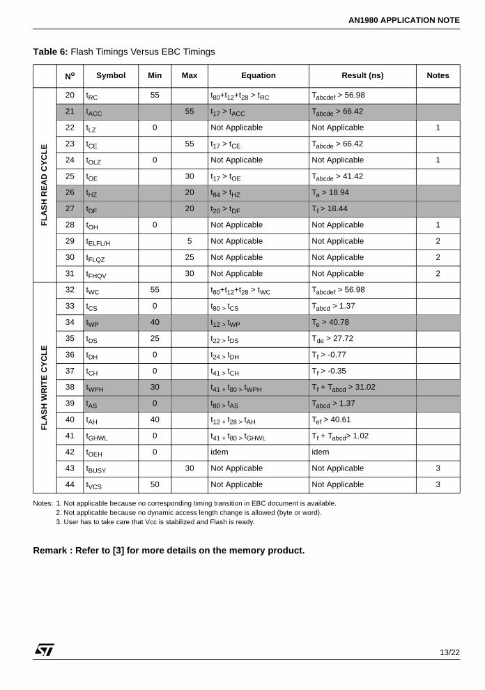
Table 6: Flash Timings Versus EBC Timings
Notes: 1. Not applicable because no corresponding timing transition in EBC document is available.2. Not applicable because no dynamic access length change is allowed (byte or word).3. User has to take care that Vcc is stabilized and Flash is ready.
Remark : Refer to [3] for more details on the memory product.
No Symbol Min Max Equation Result (ns) Notes
FL
AS
H R
EA
D C
YC
LE
20 tRC 55 t80+t12+t28 > tRC Tabcdef > 56.98
21 tACC 55 t17 > tACC Tabcde > 66.42
22 tLZ 0 Not Applicable Not Applicable 1
23 tCE 55 t17 > tCE Tabcde > 66.42
24 tOLZ 0 Not Applicable Not Applicable 1
25 tOE 30 t17 > tOE Tabcde > 41.42
26 tHZ 20 t84 > tHZ Ta > 18.94
27 tDF 20 t20 > tDF Tf > 18.44
28 tOH 0 Not Applicable Not Applicable 1
29 tELFL/H 5 Not Applicable Not Applicable 2
30 tFLQZ 25 Not Applicable Not Applicable 2
31 tFHQV 30 Not Applicable Not Applicable 2
FL
AS
H W
RIT
E C
YC
LE
32 tWC 55 t80+t12+t28 > tWC Tabcdef > 56.98
33 tCS 0 t80 > tCS Tabcd > 1.37
34 tWP 40 t12 > tWP Te > 40.78
35 tDS 25 t22 > tDS Tde > 27.72
36 tDH 0 t24 > tDH Tf > -0.77
37 tCH 0 t41 > tCH Tf > -0.35
38 tWPH 30 t41 + t80 > tWPH Tf + Tabcd > 31.02
39 tAS 0 t80 > tAS Tabcd > 1.37
40 tAH 40 t12 + t28 > tAH Tef > 40.61
41 tGHWL 0 t41 + t80 > tGHWL Tf + Tabcd> 1.02
42 tOEH 0 idem idem
43 tBUSY 30 Not Applicable Not Applicable 3
44 tVCS 50 Not Applicable Not Applicable 3

AN1980 APPLICATION NOTE
14/22
3.1.4 - Numerical Application
The register value associated to each EBC phase is calculated using the previous selected equations set(major equations marked as bold). Maximum application performance is reached when all these parame-ters are minimized. So, as a starting point, just assign to each parameter the smallest possible value :PHa = 0, PHb = 1, PHc = 0, PHd = 0, PHe = 1, PHf_read = 0, PHf_write = 0. Then, resolve all the equations (Ta,Tb, Tc, Td, Te, Tf_read, Tf_write) starting from the easiest equation (1 unknown value) to the most difficult one.
For example, considering SRAM memory equations, it is easy to determine Te for a given frequency withthe following equation (equation number 4) :
Te > 17.17 ns (Te = 2 x 10 ns @100Mhz, Te = 3 x 7.5 ns @133Mhz).
Depending on clock frequency (100Mhz or 133Mhz), two TCONCSx register configurations which verifyall these equations are shown in Table Notes:.
Notes: 1. Tf , considering (8), should be greater than 0. Tf is replaced by Ta according to the fact that no mode change (for instance : fromdemux to mux) is allowed when the CS is activated. The only data contention may appear in case of CS change. Thus, by addingTa, all data contentions are avoided.
2. Successive write configuration, since Tf cannot be greater than 3 wait states, 1 wait state is added to Tb. Nevertheless, the usershould consider two values for this parameter regarding the access type (write or read). The proposal is to reduce to the minimumthe parameter in case of read and to increase it for a write. A dynamic switching occurs each time the user code enters and exitsa flash programmation section allowing to reduce read access penalty.
3. According to (21), a wait state is added on Te to fit requirement.
4. The A phase cycles are only inserted when the current access is not using the same CS than the previous one. In conclusion, twovalues (min. et max.) are calculated depending on this assertion.
Table 7: Wait States Summary
SRAM Memory FLASH Memory
Fcpu
Tcpu
100Mhz
10ns
133Mhz
7.5ns
Equations used 100Mhz
10ns
133Mhz
7.5ns
Equations used
A phase 1 1 (8)(17) 1 2 3 (26)(27) 1
B phase 1 1 2 1 2 (38) 2
C phase 0 0 0 0
D phase 0 0 0 0
E phase 2 3 4 5 7 (34)(21) 3
F phase read 0 0 1 0 0 1
F phase write 0 0 1 3 3 (38) 2
Twrite min 4 3 4 9 12
max 4 4 5 11 15
Tread min 4 3 4 6 9
max 4 4 5 8 12

AN1980 APPLICATION NOTE
15/22
4 - PRACTICAL APPROACH
4.1 - Board Activation
To verify the EBC registers configuration previously calculated, a Super10 R303 Bond Out evaluationboard is used. The evaluation board provides :
– 128K x 16-bit Data FLASH,
– 512K x 16-bit SRAM.
The memory mapping for both memories is set to :
– SRAM : 40 0000h - 4F FFFFh,
– FLASH : 50 0000h - 53 FFFFh.
The board configuration is as follows :
– Normal mode selected (boot-strap loader mode selected - BSL on, starting in internal program memory- EA off),
– Master frequency Fcpu is 133 Mhz,
– CS0 signal selects on-board FLASH memory bank (16 bit demultiplexed),
– CS1 signal selects on-board SRAM memory bank (16 bit demultiplexed, WRL / WRH mode),
– Serial link is used by the host system to debug the application,
– P2[1:0] respectively connected to LED[1:0].
The EBC registers initialization is :
– EBCMOD0 = 0x0928h
– FCONCS0 = 0x0021h
– FCONCS1 = 0x0021h
– ADDRSEL1 = 0x4008h
4.2 - How to Set-up EBC Registers
A Super10 application program is generally made of at least three different sections :
– SYSTEM INITIALISATION
– APPLICATION INITIALISATION
– MAIN PROGRAM
In the first section, all the system registers are initialized to ensure a correct Super10 behavior. These ini-tializations are mandatory. The EINIT instruction ends this section. In the next one, all application dedi-cated initializations are done. The last section contains the user code.
The EBC registers are initialized in the SYSTEM INIT section before the EINIT instruction. An example ofEBC registers initialization is given in page 18.
The Tasking toolchain provides everything needed to initialize these registers without difficulties. A dedi-cated tool menu "EDE-> Bus configuration" allows the user to enter each registers value in an easilyunderstandable way (Refer to [4] for more details).
AN1980 APPLICATION NOTE
16/22
5 - TIMING VALIDATION
5.1 - Methodology
The previous EBC registers configuration must deliver the maximum bus bandwidth without data integritytroubles. It is not possible to verify this last conclusion due to the fact that we do not use the evaluationboard in worst case conditions (125°C for example). To stress the timings for verification purposes, asolution is to demonstrate that for a more restrictive configuration (parameters set to the minimum), someerrors occur. The idea is to write and read each external memory location and check that the pattern pre-viously written is the same as the one read. Two EBC configurations will be used :
– Minimal configuration : Tb = 1, Te = 1, the others parameters are reset.
– Calculated configuration : see Table Notes:.
Pratically, the minimal configuration should lead to a fail status and the calculated configuration not.
The Flash memory and the SRAM memory are treated differently. The Flash memory need to be initial-ized with an utility tool "Flash166" provided by the board manufactor whereas the SRAM memory is initial-ized by the firmware application. The Flash initialization pattern is a draughtboard (i.e: 10101010) foreven addresses and an inverted draughtboard (i.e: 01010101) for odd addresses. Only read operationare performed on the Flash memory after the initialisation process is done.
The test program is given in page 19.
5.2 - Results
The test program is run twice using the minimal and the calculated configurations. The LED 0 and 1, onthe R303 evaluation board, give respectively the Flash and the SRAM test status. A lit LED indicates thatthe test passes.
The results are as follows :
The SRAM memory test does not fail even if we use the minimal configuration. A failed test will beobserved only if we use the R303 evaluation board in worst case conditions (process, voltage, tempera-ture).
Table 8: Memories Test Results
Memory Minimal Configuration Calculated Configuration
FLASH Failed Passed
SRAM Passed Passed
AN1980 APPLICATION NOTE
17/22
6 - CONCLUSION
This note has described a way of setting up the EBC registers to maximize External Bus performance fortwo given memories. The flexibility of the Super10 EBC allows the user to use any kind of memory andtailor the different parameters accordingly to reach high performance.
7 - REFERENCES
[1] Super10 User’s manual (M345/M350, release 1.3)
[2] uPD434008AL Datasheet
[3] M29W200BT/BB Datasheet
[4] Tasking Toolchain & Documentation, release 7.5r2
[5] Forth System Super10_3 Documentation

AN1980 APPLICATION NOTE
18/22
8 - APPENDIX
THE SOFTWARE INCLUDED IN THIS NOTE IS FOR GUIDANCE ONLY. STMICROELECTRONICSSHALL NOT BE HELD LIABLE FOR ANY DIRECT, INDIRECT OR CONSEQUENTIAL DAMAGES WITHRESPECT TO ANY CLAIMS ARISING FROM USE OF THE SOFTWARE.
8.1 - EBC Registers Initialization Example - Fcpu = 133Mhz
MOV R0, #00928h ; 24 address bits
MOV EBCMOD0, R0 ; 2 chip select lines
; Ready pin enabled (active low)
; WRLn and WRHn (not WRn and BHEn)
; All EBC pins enabled (master mode)
MOV R0, #21h ; 16 demux
MOV FCONCS0, R0 ; Ready disabled
MOV R0, #6187h ; A = 3 clks No CS switch off time
MOV TCONCS0, R0 ; B = 2 clks ALE length
; C = 0 clk No R/W delay
; D = 0 clk
; E = 7 clks Wait state time
; F = 0 clk Read memory tristate time
; F = 3 clks Write memory tristate time
MOV R0, #21h ; 16 demux
MOV FCONCS1, R0 ; Ready disabled
MOV R0, #0081h ; A = 1 clk No CS switch off time
MOV TCONCS1, R0 ; B = 1 clk ALE length
; C = 0 clk No R/W delay
; D = 0 clk
; E = 3 clks Wait state time
; F = 0 clk (R and W) No memory tristate time
MOV R0, #4008h ; 1024 Kbyte window
MOV ADDRSEL1, R0 ; 400000h to 4FFFFF...EINIT ; System init end

AN1980 APPLICATION NOTE
19/22
8.2 - Validation Test Program
/*----------------------------------------------------------------- **
** EBC Test program with Super10 R303/M345 **
** **
** Programming task: **
** Initialize EBC registers via graphical interface **
** Verify that read and write accesses are performed correctly on **
** SRAM and FLASH memory at full speed. **
** **
** Outputs: **
** Port 2.0 = driving LED #1, SRAM Ok if LED #1 lit **
** Port 2.1 = driving LED #2 FLASH ok if LED #2 lit **
**----------------------------------------------------------------- */
#include <REGSUPER10BO.H>
#define SRAM_SIZE 524288 /* 512k * 16 bits */
#define FLASH_SIZE 131072 /* 128k * 16 bits */
/********************************************************************/
#pragma class hb=FASTSRAM
#pragma combine hb=P//A0x400000
#pragma align hb=word
_huge unsigned int sram_array[SRAM_SIZE];
#pragma class hb=SLOWFLASH
#pragma combine hb=P//A0x500000
#pragma align hb=word
_huge unsigned int flash_array[FLASH_SIZE];
#pragma default_attributes
const unsigned int inv_draughtboard_vec = 0x5555;
const unsigned int draughtboard_vec = 0xAAAA;
unsigned int sram_test_ok = 1;
unsigned int flash_test_ok = 1;
sfrbit DP20 _atbit (DP2,0); /* Output, LED #1 */
sfrbit DP21 _atbit (DP2,1); /* Output, LED #2 */
sfrbit P20 _atbit (P2,0);
sfrbit P21 _atbit (P2,1);
/********************************************************************/
AN1980 APPLICATION NOTE
20/22
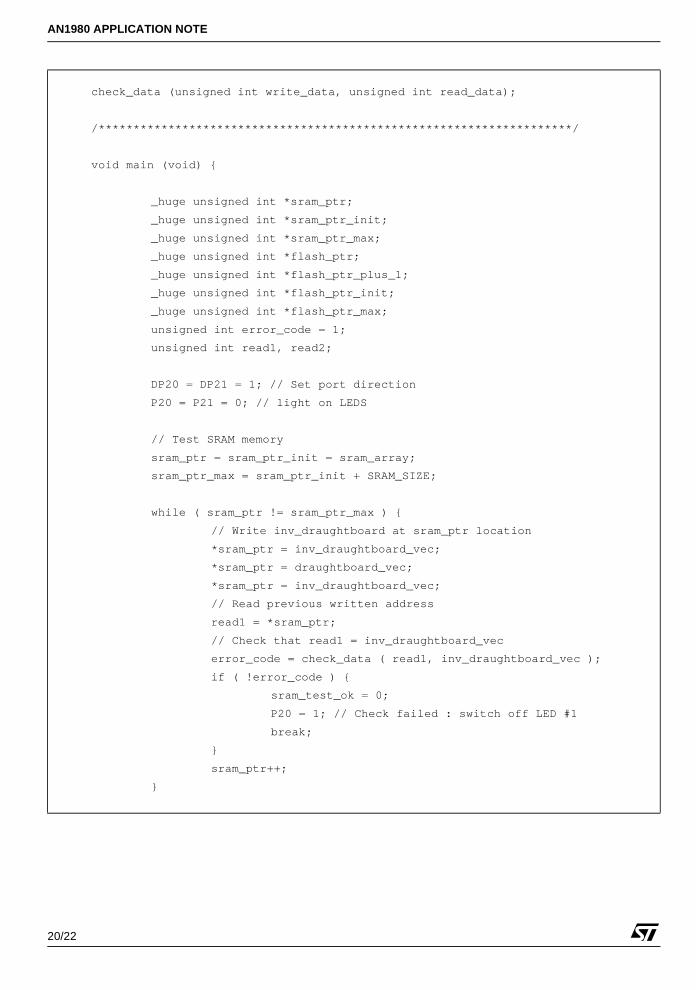
check_data (unsigned int write_data, unsigned int read_data);
/********************************************************************/
void main (void) {
_huge unsigned int *sram_ptr;
_huge unsigned int *sram_ptr_init;
_huge unsigned int *sram_ptr_max;
_huge unsigned int *flash_ptr;
_huge unsigned int *flash_ptr_plus_1;
_huge unsigned int *flash_ptr_init;
_huge unsigned int *flash_ptr_max;
unsigned int error_code = 1;
unsigned int read1, read2;
DP20 = DP21 = 1; // Set port direction
P20 = P21 = 0; // light on LEDS
// Test SRAM memory
sram_ptr = sram_ptr_init = sram_array;
sram_ptr_max = sram_ptr_init + SRAM_SIZE;
while ( sram_ptr != sram_ptr_max ) {
// Write inv_draughtboard at sram_ptr location
*sram_ptr = inv_draughtboard_vec;
*sram_ptr = draughtboard_vec;
*sram_ptr = inv_draughtboard_vec;
// Read previous written address
read1 = *sram_ptr;
// Check that read1 = inv_draughtboard_vec
error_code = check_data ( read1, inv_draughtboard_vec );
if ( !error_code ) {
sram_test_ok = 0;
P20 = 1; // Check failed : switch off LED #1
break;
}
sram_ptr++;
}
AN1980 APPLICATION NOTE
21/22
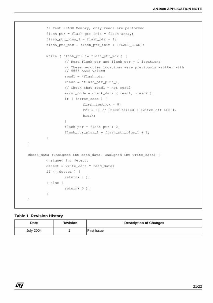
Table 1. Revision History
Date Revision Description of Changes
July 2004 1 First Issue
// Test FLASH Memory, only reads are performed
flash_ptr = flash_ptr_init = flash_array;
flash_ptr_plus_1 = flash_ptr + 1;
flash_ptr_max = flash_ptr_init + (FLASH_SIZE);
while ( flash_ptr != flash_ptr_max ) {
// Read flash_ptr and flash_ptr + 1 locations
// These memories locations were previously written with // 5555 AAAA values
read1 = *flash_ptr;
read2 = *flash_ptr_plus_1;
// Check that read1 = not read2
error_code = check_data ( read1, ~read2 );
if ( !error_code ) {
flash_test_ok = 0;
P21 = 1; // Check failed : switch off LED #2
break;
}
flash_ptr = flash_ptr + 2;
flash_ptr_plus_1 = flash_ptr_plus_1 + 2;
}
}
check_data (unsigned int read_data, unsigned int write_data) {
unsigned int detect;
detect = write_data ^ read_data;
if ( !detect ) {
return( 1 );
} else {
return( 0 );
}
}
AN1980 APPLICATION NOTE
22/22
AN
1980
.FM
22
The present note which is for guidance only, aims at providing customers with information regarding their productsin order for them to save
time. As a result, STMicroelectronics shall not be held liable for any direct, indirector consequential damages with respect to any claims aris-
ing from the content of such a note and/or the use made by customers of the information contained herein in connection with their products.
Information furnished is believed to be accurate and reliable. However, STMicroelectronics assumes no responsibility for the consequencesof use of such information nor for any infringement of patents or other rights of third parties which may result from its use. No license is grantedby implication or otherwise under any patent or patent rights of STMicroelectronics. Specifications mentioned in this publication are subjectto change without notice. This publication supersedes and replaces all information previously supplied. STMicroelectronics products are notauthorized for use as critical components in life support devices or systems without express written approval of STMicroelectronics.
The ST logo is a registered trademark of STMicroelectronics.All other names are the property of their respective owners
© 2004 STMicroelectronics - All rights reserved
STMicroelectronics GROUP OF COMPANIESAustralia - Belgium - Brazil - Canada - China - Czech Republic - Finland - France - Germany - Hong Kong - India - Israel - Italy - Japan -
Malaysia - Malta - Morocco - Singapore - Spain - Sweden - Switzerland - United Kingdom - United Stateswww.st.com