an1827: programming and erasing flash memory on the ... · memory in the flash array is organized...
TRANSCRIPT

Fre
esc
ale
Se
mic
on
du
cto
r, I
nc
...
Order this documentby AN1827/D
AN1827
Programming and Erasing FLASH Memoryon the MC68HC908AS60By Kim Keating, Adeela Gill, and Kazue Kikuchi
Body Electronics and Occupant SafetyMatt RutledgeNon-Volatile Memory Technology Center
Introduction
Freescale has released an innovative type of FLASH non-volatile memory(NVM) for its 8-bit M68HC08 Family of microcontrollers. This FLASHtechnology allows in-circuit reprogrammability over the entireautomotive specification range.
In-circuit reprogrammability offers these advantages:
• In-system code revision
• EPROM (erasable programmable read-only memory)replacement as a reusable code development platform
• Quick time to market with one chip for code development andproduction
• No obsolete inventory as with ROM parts
• Allows for last-minute code changes without waiting for new ROMcode lots
© Motorola, Inc., 1999 AN1827
For More Information On This Product, Go to: www.freescale.com

Application Note
F
ree
sca
le S
em
ico
nd
uc
tor,
I
Freescale Semiconductor, Inc.n
c..
.
This application note explains how to use the FLASH on theMC68HC908AS60 and provides example software for program anderase operations. The reprogramming algorithms are written in bothM68HC08 assembly code and in C code.
This code is available for download from Motorola’s SemiconductorProduct Sector’s Web site at http://mot-sps.com.
The FLASH topics covered in this application note include:
• Features
• Implementation on Motorola’s M68HC08 microcontrollers
• Functional description
• Control and block protect registers
• Charge pump
• Block protection
• Erase operation
• Page program/margin read algorithm
• Frequently asked questions
• Hardware schematic
• Assembly source code
• C source code
Features
The benefits of FLASH on the MC68HC908AS60 include:
• Single VDD power supply is utilized for program/erase.This feature simplifies program and erase with respect to EPROM(no high voltage power supply or UV (ultraviolet) oven required),reduces program and erase cycle time, and enables in-circuitreprogrammability.
AN1827
2 For More Information On This Product,
Go to: www.freescale.com

Application NoteImplementation on Motorola’s M68HC08 Microcontrollers
F
ree
sca
le S
em
ico
nd
uc
tor,
I
Freescale Semiconductor, Inc.n
c..
.
• The FLASH manufacturing process is fully compatible with theEEPROM (electrically erasable, programmable read-onlymemory) process.This process compatibility allows the functionality of both FLASHand EEPROM non-volatile memories on the same chip.
• Meets automotive specificationsUnlike many competing microcontrollers with FLASH, this FLASHcan operate and meet reliability requirements for the automotivespace. The FLASH on the MC68HC908AS60 will read, program,and erase over the –40°C to 125°C temperature range. Thespecified program/erase endurance and data retention lifetime arevalid over the entire temperature range.
• Multiple arraysMultiple arrays on the MC68HC908AS60 allow code execution outof one array while programming or erasing the other array.
• Smart programming algorithmUse of the smart programming algorithm ensures minimumprogram time while still guaranteeing automotive environmentoperation and data retention.
Implementation on Motorola’s M68HC08 Microcontrollers
The specific FLASH technology found on the MC68HC908AS60 isknown as FLASH 2TS, in reference to its 2-transistor source-select bitcell. FLASH 2TS is commonly found on Motorola’s M68HC08 Family ofmicrocontrollers, but it is not the exclusive FLASH technology for theHC08 core. The FLASH 2TS technology discussed in this applicationnote is referred to generically as FLASH.
This FLASH technology is available in array sizes between 2 Kbytes and32 Kbytes. For parts requiring more than 32 Kbytes, multiple arrays ofany size between 2 Kbytes and 32 Kbytes, with 2-Kbyte boundaries, canbe placed on a chip. Typically, only one charge pump is used on partswith multiple arrays. This constrains program or erase operations to onearray at a time, but conserves die area.
AN1827
3 For More Information On This Product,
Go to: www.freescale.com

Application Note
F
ree
sca
le S
em
ico
nd
uc
tor,
I
Freescale Semiconductor, Inc.n
c..
.
The FLASH bit cell consists of two transistors in series, referred to as theselect-gate and control-gate transistors. The floating gate is associatedwith the control gate transistor and stores charges which represent thetwo different data states of the memory. The high threshold condition ofthe bit cell is the erased state and the low threshold condition is theprogrammed state. The select gate prevents bit cell leakage ofunselected wordlines during read operations when the floating gate isprogrammed.
Although the size and shape of the array is mostly transparent to theuser, it does help when determining the "cared addresses" during theerase algorithm. The term and function of "cared addresses" areexplained in the Erase Operation of this application note. For now, it isimportant to know that the cared addresses determine exactly whichblock will erase during the erase operation.
More importantly, the size and shape of the memory array may alter thesize of the programming page. The term page refers to the number ofconsecutive bytes that are programmed during a page program/marginread operation. On larger memory arrays, like the two arrays found onthe MC68HC908AS60, one page equals eight bytes. As the array isscaled down, the page is proportionally scaled to either four, two, or onebyte(s). This will affect the programming algorithm that appears later inthis application note.
The only other obvious difference in implementation of the FLASH arrayis the size of the blocks that can be protected against an undesiredprogram or erase operation. Again, this depends on the size of thememory on the microcontroller. Check the appropriate documentationfor each specific microcontroller to determine the size of the memoryarray, the page program size, and the erase block sizes.
AN1827
4 For More Information On This Product,
Go to: www.freescale.com

Application NoteFunctional Description
F
ree
sca
le S
em
ico
nd
uc
tor,
I
Freescale Semiconductor, Inc.n
c..
.
Functional Description
The FLASH memory on the MC68HC908AS60 physically consists of twoindependent arrays with two bytes of block protection and additionalbytes of user vectors. An erased bit reads as a logic 0 and aprogrammed bit reads as a logic 1. Program and erase operations arefacilitated through control bits in memory mapped registers. Details forthese operations appear later in this application note.
Memory in the FLASH array is organized into pages within rows. Thereare eight pages of memory per row with eight bytes per page. Theminimum erase block size is a single row, 64 bytes. Programming isperformed on a per-page basis, eight bytes at a time. The addressranges for the user memory, control registers, block protect registers,and vectors are listed here.
The FLASH memory map on the MC68HC908AS60 consists of:
• $0450–$05FF, FLASH-2 array, 432 bytes
• $0E00–$7FFF, FLASH-2 array, 29,184 bytes
• $8000–$FDFF, FLASH-1 array, 32,256 bytes
• $FE0B, FLASH-1 control register, FLCR1
• $FE11, FLASH-2 control register, FLCR2
• $FF80, FLASH-1 block protect register, FLBPR1
• $FF81, FLASH-2 block protect register, FLBPR2
• $FFDA–$FFFF, FLASH-1 vector space, 38 bytes
To program the FLASH, each page must be erased before it isprogrammed. The erase block sizes are found in Erase Operation.
The four 64-byte row address boundaries for the MC68HC908AS60 are:
• $xx00–$xx3F
• $xx40–$xx7F
• $xx80–$xxBF
• $xxC0–$xxFF
AN1827
5 For More Information On This Product,
Go to: www.freescale.com

Application Note
F
ree
sca
le S
em
ico
nd
uc
tor,
I
Freescale Semiconductor, Inc.n
c..
.
When programming the FLASH, exact program time must be used toprogram a page. Excessive program time can result in a program disturbcondition, in which case an erased bit on the row being programmedbecomes unintentionally programmed. Program disturb is avoided byusing an iterative program and margin read technique known as thesmart programming algorithm. The smart programming algorithm isrequired whenever programming the FLASH. See PageProgram/Margin Read Algorithm.
NOTE: A security feature prevents viewing of the FLASH contents.1
Programming tools are available from Freescale. Contact a local Freescalerepresentative for more information.
Control and Block Protect Registers
Each FLASH array has two registers that control its operation, theFLASH control register (FLCR) and the FLASH block protect register(FLBPR). See Figure 1 and Figure 2.
There are two FLASH control registers, FLCR1 and FLCR2, forFLASH-1 and FLASH-2 arrays, respectively.
• $FE0B — FLASH-1 control register (FLCR1)
• $FE11 — FLASH-2 control register (FLCR2)
1. No security feature is absolutely secure. However, Motorola’s strategy is to make reading orcopying the FLASH difficult for unauthorized users.
Bit 7 6 5 4 3 2 1 Bit 0
Read:FDIV1 FDIV0 BLK1 BLK0 HVEN MARGIN ERASE PGM
Write:
Reset: 0 0 0 0 0 0 0 0
Figure 1. FLASH Control Register (FLCR)
AN1827
6 For More Information On This Product,
Go to: www.freescale.com

Application NoteControl and Block Protect Registers
F
ree
sca
le S
em
ico
nd
uc
tor,
I
Freescale Semiconductor, Inc.n
c..
.
FDIV1 — Frequency Divide Control Bit
This read/write bit together with FDIV0 selects the factor by whichthe charge pump clock is divided from the bus clock. See ChargePump.
FDIV0 — Frequency Divide Control Bit
This read/write bit together with FDIV1 selects the factor by whichthe charge pump clock is divided from the bus clock. See ChargePump.
BLK1 — Block Erase Control Bit
This read/write bit together with BLK0 allows erasing of blocks ofvarying sizes. See Erase Operation for a description of availableblock sizes.
BLK0 — Block Erase Control Bit
This read/write bit together with BLK1 allows erasing of blocks ofvarying sizes. See Erase Operation for a description of availableblock sizes.
HVEN — High-Voltage Enable Bit
This read/write bit enables the charge pump to drive high voltagesfor program and erase operations in the array. HVEN can be setonly if either PGM = 1 or ERASE = 1 and the proper sequence forerase or page program/margin read is followed.
1 = High voltage enabled to array and charge pump on0 = High voltage disabled to array and charge pump off
MARGIN — Margin Read Control Bit
This read/write bit configures the memory for the margin readoperation. MARGIN cannot be set if HVEN = 1. MARGIN willautomatically clear (MARGIN = 0) if asserted when HVEN = 1.
1 = Margin read operation selected0 = Margin read operation unselected
AN1827
7 For More Information On This Product,
Go to: www.freescale.com

Application Note
F
ree
sca
le S
em
ico
nd
uc
tor,
I
Freescale Semiconductor, Inc.n
c..
.
ERASE — Erase Control Bit
This read/write bit configures the memory for the erase operation.ERASE is interlocked with the PGM bit such that both bits cannotbe set at the same time.
1 = Erase operation selected0 = Erase operation unselected
PGM — Program Control Bit
This read/write bit configures the memory for the programoperation. PGM is interlocked with the ERASE bit such that bothbits cannot be set at the same time.
1 = Program operation selected0 = Program operation unselected
There are two FLASH block protect registers, FLBPR1 and FLBPR2, forFLASH-1 and FLASH-2 arrays, respectively.
• $FF80 — FLASH-1 block protect register (FLBPR1)
• $FF81 — FLASH-2 block protect register (FLBPR2)
BPR3 — Block Protect Register Bit 3
This bit protects the memory contents in the address range:FLASH-1 $C000 to $FFFF or FLASH-2 $4000 to $7FFF.
1 = Address range protected from erase or program0 = Address range open to erase or program
Bit 7 6 5 4 3 2 1 Bit 0
Read:DC DC DC DC BPR3 BPR2 BPR1 BPR0
Write:
Reset: NV NV NV NV NV NV NV NV
NV — Non-volatile, 1 if programmed, 0 if erasedDC — Don’t care
Figure 2. FLASH Block Protect Register (FLBPR)
AN1827
8 For More Information On This Product,
Go to: www.freescale.com

Application NoteCharge Pump
F
ree
sca
le S
em
ico
nd
uc
tor,
I
Freescale Semiconductor, Inc.n
c..
.
BPR2 — Block Protect Register Bit 2
This bit protects the memory contents in the address range:FLASH-1 $A000 to $FFFF or FLASH-2 $2000 to $7FFF.
1 = Address range protected from erase or program0 = Address range open to erase or program
BPR1 — Block Protect Register Bit 1
This bit protects the memory contents in the address range:FLASH-1 $9000 to $FFFF or FLASH-2 $1000 to $7FFF.
1 = Address range protected from erase or program0 = Address range open to erase or program
BPR0 — Block Protect Register Bit 0
This bit protects the memory contents in the address range:FLASH-1 $8000 to $FFFF or FLASH-2 $0450 to $7FFF.
1 = Address range protected from erase or program0 = Address range open to erase or program
Charge Pump
The internal charge pump is required for program, margin read, anderase operations of the FLASH.
The charge pump is a dynamic circuit that uses a specific clockingsequence of capacitors and switches to generate voltages higher inmagnitude than VDD. This charge pump design requires a clockfrequency range between 1.8 MHz and 2.5 MHz to operate the FLASHcorrectly. The charge pump clock is derived from the bus clock. TheFDIV1 and FDIV0 bits in the FLASH control register are able to dividethe internal bus clock by 1, 2, or 4 to generate the charge pump clock.These divide ratios allow enough tolerance for several commonlyavailable crystal frequencies.
See Table 1 for common divide ratios based upon internal busfrequency.
AN1827
9 For More Information On This Product,
Go to: www.freescale.com

Application Note
F
ree
sca
le S
em
ico
nd
uc
tor,
I
Freescale Semiconductor, Inc.n
c..
.
NOTE: When FLASH memory is programmed/erased with the PLL on or inmonitor mode, bus frequency is not always the same as the externalclock frequency divided by four. Since the charge pump frequency isderived from the bus frequency, confirm the bus frequency being used.
NOTE: If the charge pump frequency is not between 1.8 MHz and 2.5 MHz,Freescale does not guarantee the operation, electrical, or reliabilityspecifications of the FLASH.
The HVEN bit in the FLASH control register enables the charge pump togenerate high voltages for program and erase modes. The charge pumpalso generates a regulated voltage for the margin read mode in thesmart programming algorithm. During programming, the HVEN bitshould be asserted only for 1 ms to 1.2 ms at a time. (See Figure 8.)Asserting HVEN for longer than 1.2 ms at a time risks program disturb,where an erased bit on the same row becomes unintentionallyprogrammed. Program disturb is a common soft fault and can berecovered by erasing the row and reprogramming using the smartprogramming algorithm.
Table 1. Bus Frequency Divide Ratios for Charge Pump Clock
fBus (MHz) FDIV1 FDIV0 Division fPump (MHz)
2.000 0 0 1 2.000
2.4576 0 0 1 2.4576
4.000 0 1 2 2.000
4.9152 0 1 2 2.4576
8.000 1 1 4 2.000
8.400 1 1 4 2.100
AN1827
10 For More Information On This Product,
Go to: www.freescale.com

Application NoteBlock Protection
F
ree
sca
le S
em
ico
nd
uc
tor,
I
Freescale Semiconductor, Inc.n
c..
.
Block Protection
To protect the contents in the FLASH array from being inadvertentlyprogrammed or erased by run-away code in the user application, theFLASH block protect register option was implemented. This register iscomposed of two non-volatile bytes within the FLASH-1 array, with onebyte per FLASH array. Once the block protect bits are set in the FLBPRregisters, the defined address ranges are protected from beingprogrammed or erased. See Control and Block Protect Registers fora description of address ranges.
The FLBPR register itself can be erased or programmed only with anexternal voltage VHI on the IRQ pin. VHI is defined as a voltage betweenVDD + 2 V and VDD + 4 V. Use of the block protect register is anadditional measure to prevent inadvertent programming or erasing ofFLASH contents in an application.
NOTE: To implement in-system program or erase for a protected area ofFLASH, a high voltage signal must be routed to the IRQ pin.
Erase Operation
To erase a FLASH array, follow this 9-step procedure. Figure 3 showsa flowchart of this procedure.
1. Set ERASE = 1, and set the BLK bits and FDIV bits.
ERASE = 1 configures the FLASH memory for an erase operation.The BLK bits determine the erase block size: whole array, halfarray, 512 bytes or 64 bytes. The FDIV bits determine the chargepump frequency. The frequency should be selected within therange between 1.8 MHz and 2.5 MHz. Refer to Charge Pump.
2. Read the FLASH block protect register.
The block protect registers must be read before high voltage canbe enabled. If the desired address set in step 3 is in a protectedblock, erase will fail.
AN1827
11 For More Information On This Product,
Go to: www.freescale.com

Application Note
F
ree
sca
le S
em
ico
nd
uc
tor,
I
Freescale Semiconductor, Inc.n
c..
.
3. Write to any FLASH address within the block address rangedesired.
The "cared" bits for the FLASH address are latched and used todetermine the address range that will be erased. The details arediscussed later in this section.
4. Set HVEN = 1.
a. Internal high voltage is applied for erasing.
5. Wait for a time, tErase.
tErase is the block erase time.
6. Set HVEN = 0.
Internal high voltage is disabled.
7. Wait for a time, tKill.
This allows the high voltage to be discharged completely.
8. Set ERASE = 0.
Disable the erase operation.
9. Wait for a time, tHVD.
After a time, tHVD, the memory can be accessed in normal readmode.
NOTE: If bulk erase is attempted on a FLASH array where either part or all ofthe array is block protected, then none of the FLASH memory in thatarray is erased.
AN1827
12 For More Information On This Product,
Go to: www.freescale.com

Application NoteErase Operation
F
ree
sca
le S
em
ico
nd
uc
tor,
I
Freescale Semiconductor, Inc.n
c..
.
Figure 3. FLASH Erase Operation Flowchart
2. READ BLOCK PROTECTREGISTERS (FLBPR)
1. SET ERASE BIT, BLK BITSAND FDIV BITS
ERASE FLASH
3. WRITE TO AN ADDRESS IN THEBLOCK TO ERASE
4. SET HVEN BIT
5. WAIT A TIME, tErase
6. CLEAR HVEN BIT
7. WAIT A TIME, tKill
8. CLEAR ERASE BIT
9. WAIT A TIME, tHVD
ERASE OPERATIONCOMPLETE
AN1827
13 For More Information On This Product,
Go to: www.freescale.com

Application Note
F
ree
sca
le S
em
ico
nd
uc
tor,
I
Freescale Semiconductor, Inc.n
c..
.
Although the overall procedure is relatively simple, step 3 could usesome clarification. Since the specified address is any address within theblock to erase, the microcontroller must somehow know exactly whichmemory range to erase. This is where the "cared address" becomesimportant.
In step 2, the size of the block to erase is set by writing to the BLK bitsin the FLCR. Table 2 shows the various block sizes which can be erasedin one erase operation.
When an address is specified in step 3, certain address lines are latchedpertaining to this block size, and they establish the start and endaddresses of the block. The larger the erase block, the smaller the sizeof the cared address.
For example, if the BLK bits are set such that the erase block size is asingle row (BLK0 = BLK1 = 1), and the address $9AF0 is specified instep 3, then bits 15–6 of $9AF0 are the "cared addresses." Therefore,the values of these address bits are fixed.
Table 2. Erase Block Sizes
BLK1 BLK0 Block Size Cared Addresses
0 0 Full array: 32 Kbytes A15
0 1 One-half array: 16 Kbytes A15–A14
1 0 Eight rows: 512 bytes A15–A9
1 1 Single row: 64 bytes A15–A6
Hex 9 A F 0
Bit No. 15 14 13 12 11 10 9 8 7 6 5 4 3 2 1 0
Binary 1 0 0 1 1 0 1 0 1 1 1 1 0 0 0 0
Figure 4. Cared Address Example $9AF0
Cared Addresses
AN1827
14 For More Information On This Product,
Go to: www.freescale.com

Application NoteErase Operation
F
ree
sca
le S
em
ico
nd
uc
tor,
I
Freescale Semiconductor, Inc.n
c..
.
As a result, the beginning address of the block which will be erased is:
The end address of the block which will be erased is:
This results in erasing 64 bytes from address $9AC0 to $9AFF.
NOTE: All memory arrays are shaped differently, so one row may not equal 64bytes like on the MC68HC908AS60. Refer to the appropriatedocumentation for the pertinent device and apply these same principles.
Hex 9 A C 0
Bit No. 15 14 13 12 11 10 9 8 7 6 5 4 3 2 1 0
Binary 1 0 0 1 1 0 1 0 1 1 0 0 0 0 0 0
Figure 5. Erase Beginning Address for Example
Hex 9 A F F
Bit No. 15 14 13 12 11 10 9 8 7 6 5 4 3 2 1 0
Binary 1 0 0 1 1 0 1 0 1 1 1 1 1 1 1 1
Figure 6. Erase End Address for Example
Cared Addresses
Cared Addresses
AN1827
15 For More Information On This Product,
Go to: www.freescale.com

Application Note
F
ree
sca
le S
em
ico
nd
uc
tor,
I
Freescale Semiconductor, Inc.n
c..
.
Page Program/Margin Read Algorithm
In the MC68HC908AS60, programming of the FLASH memory is doneon a page-by-page basis. A page consists of eight bytes, fromaddresses $XXX0 to $XXX7 or from $XXX8 to $XXXF. Therefore, theaddresses of the first byte in a page must be $XXX0 or $XXX8.
This FLASH memory requires the smart programming algorithm. Thesmart programming algorithm is defined as an iterative program andmargin read sequence. Every page program operation is followed by amargin read until the data is programmed successfully. The margin readstep of the smart programming algorithm is used to ensure programmedbits are programmed to sufficient margin for data retention over thedevice’s lifetime.
The smart programming algorithm steps are shown here and in theFigure 7 flowchart.
1. Initialize attempt counter.
The sequence will be attempted until the count reaches flsPulses.
2. Set PGM = 1 and set FDIV bits.
PGM = 1 configures the FLASH memory for a program operationand enables the latching of the address and data forprogramming. The FDIV bits determine the charge pumpfrequency. The frequency should be selected within the rangebetween 1.8 MHz and 2.5 MHz. Refer to Charge Pump.
3. Read the FLASH block protect register.
The block protect register must be read before high voltage can beenabled. If the desired address is in a protected block, theprogramming will fail.
4. Write data to the page being programmed (typically 8 bytes).
This requires separate write operations for each byte and theaddresses of the page must be $XXX0 to $XXX7, or $XXX8 to$XXXF.
AN1827
16 For More Information On This Product,
Go to: www.freescale.com

Application NotePage Program/Margin Read Algorithm
F
ree
sca
le S
em
ico
nd
uc
tor,
I
Freescale Semiconductor, Inc.n
c..
.
5. Set HVEN = 1.
Internal high voltage is applied for programming.
6. Wait for a time, tStep.
tStep is the time high voltage is applied for every program pulse.
7. Set HVEN = 0.
Internal high voltage is disabled.
8. Wait for a time, tHVTV.
Wait for programming voltages to dissipate before margin reading.
9. Set MARGIN = 1.
This configures the FLASH memory for margin read operation.
10. Wait for a time, tVTP.
Time to discharge the margin read voltage.
11. Set PGM = 0.
This step disables the programming operation.
12. Wait for a time, tHVD.
After a time, tHVD, the memory can be accessed in normal readmode.
13. Read programmed data (margin read process).
This requires separate read operations for each byte.
14. Compare margin read data with data written in Step 4.
This requires separate read operations for each byte.
15. Clear the MARGIN bit.
Disable the margin read operation.
16. Increment attempt counter since programming was notsuccessful.
17. If any byte of programmed data does not match the margin readdata, then there are two options. If the count is less than themaximum (flsPulses(); return to step 2 to repeat programming of thesame page. If the attempt to program count has reached flsPulses,the programming operation has failed.
AN1827
17 For More Information On This Product,
Go to: www.freescale.com

Application Note
F
ree
sca
le S
em
ico
nd
uc
tor,
I
Freescale Semiconductor, Inc.n
c..
.
Figure 7. FLASH Smart Programming Algorithm Flowchart
2. SET PGM BIT AND FDIV BITS
8. WAIT A TIME, tHVTV
10. WAIT A TIME, tVTP
5. SET HVEN BIT
11. CLEAR PGM BIT
9. SET MARGIN BIT
12. WAIT A TIME, tHVD
16. INCREMENT ATTEMPT COUNTER
YES
NO
YES
NO
PROGRAMMING OPERATIONFAILED
PROGRAMMING OPERATIONCOMPLETE
4. WRITE DATA TO SELECTED PAGE
6. WAIT A TIME, tStep
7. CLEAR HVEN BIT
13. MARGIN READ PAGE OF DATA15. CLEAR MARGIN BIT
OF MARGIN READ DATAEQUAL TO
WRITE DATA17. ATTEMPT COUNT
EQUAL TOflsPulses
3. READ FLBPR
CLEAR MARGIN BIT
14. ALL BYTES
1. INITIALIZE ATTEMPT COUNTER TO 0
PROGRAMMING FLASH
Notes:1) This algorithm is mandatory for
programming the FLASH.2) This page program algorithm assumes
the page(s) to be programmed areinitially erased.
?
?
AN1827
18 For More Information On This Product,
Go to: www.freescale.com

Application NotePage Program/Margin Read Algorithm
F
ree
sca
le S
em
ico
nd
uc
tor,
I
Freescale Semiconductor, Inc.n
c..
.
Fig
ure
8. T
imin
g D
iag
ram
of
On
e P
age
Pro
gra
m-M
arg
in R
ead
Ste
p in
th
e S
mar
t P
rog
ram
min
g A
lgo
rith
m
PG
M
FD
IV1
FD
IV0
IT12
IAB
IDB
MA
RG
IN
HV
EN
IRW
...
...
...
...
...
...
...
...
...
23
45
67
89
10
11
12
13
14
15
t S
tep
t
HV
TV
tV
TP
tH
VD
...
...
...
...
...
...
...
...
...
...
...
...
...
...
... ...
...
ST
EP
2.
3.
4.
5.
6.
7.
8.
9.
10.
11.
12.
13.
1.
INIT
IALIZ
E A
TT
EM
PT
CO
UN
TE
R (
NO
T S
HO
WN
)
SE
T P
GM
AN
D F
DIV
BIT
S
RE
AD
FLB
PR
WR
ITE
DAT
A T
O S
ELE
CT
ED
PA
GE
SE
T H
VE
N B
IT
WA
IT A
TIM
E,t S
tep
CLE
AR
HV
EN
BIT
WA
IT A
TIM
E,t H
VT
V
SE
T M
AR
GIN
BIT
WA
IT A
TIM
E,t V
TP
CLE
AR
PG
M B
IT
WA
IT A
TIM
E,t H
VD
MA
RG
IN R
EA
D P
AG
E O
F D
ATA
CO
MPA
RE
MA
RG
IN R
EA
D D
ATA
TO
WR
ITE
DATA
CLE
AR
MA
RG
IN B
IT15.
14.
...
...
INTERNAL USER CONTROLLABLE
SIGNALS REGISTERS
— D
O N
OT
CA
RE
DATA
AN1827
19 For More Information On This Product,
Go to: www.freescale.com

Application Note
F
ree
sca
le S
em
ico
nd
uc
tor,
I
Freescale Semiconductor, Inc.n
c..
.
The smart programming algorithm ensures programming data retentionand minimum program time and reduces the possibility of programdisturb. The margin read operation imposes a more stringent readcondition on the bit cell so that long-term data retention is ensured. Theoperation is the same as the ordinary read operation except the marginbit is set (MARGIN = 1). However, when the margin read operation isexecuted, data is read automatically with seven additional bus cycles perbyte. This additional settling time allows sensing of the lower bit cellcurrent.
The smart programming algorithm also uses multiple short programpulses instead of using one long program pulse. Therefore, wheneverthe margin read is successful, the page programming is completed evenif the program pulses do not reach the maximum. If the program pulsesreach the maximum, it means that programming operation has failed.
NOTE: When the COP is enabled, the seven additional cycles of the marginread operation must be considered. Since the COP counter continues torun during the additional cycles, the additional cycles need to be addedto the COP feed loop.
NOTE: When the block protect bits in the FLASH block protect register are set,a portion of the memory will be locked so that no further erase orprogram operation may be performed. However, when high voltage isapplied on the IRQ pin, the whole FLASH memory is unprotected. Thedetails are described in the Control and Block Protect Registers.
AN1827
20 For More Information On This Product,
Go to: www.freescale.com

Application NoteFrequently Asked Questions
F
ree
sca
le S
em
ico
nd
uc
tor,
I
Freescale Semiconductor, Inc.n
c..
.
Frequently Asked Questions
These questions and answers are designed to help the user withfrequent concerns.
Question 1 I cannot program/erase FLASH memory at all. What should I consider tomake my program/erase code work?
Answer 1 Check the following:
• Did you use the smart programming algorithm in yourprogramming code?The smart programming algorithm ensures that the FLASH isprogrammed for sufficient data retention and in minimum programtime. Furthermore, not following this algorithm can lead tooverprogramming, which risks program disturb. The use of thesmart programming algorithm is highly recommended. (Refer toPage Program/Margin Read Algorithm.)
• Is each step of the smart programming algorithm (or erasealgorithm) performed in the right order?The sequence of the program and erase operations areinterlocked in hardware so only the prescribed order of theseoperations can occur. However, other non-FLASH operations mayoccur between the steps shown.
• Is the memory block where you want to program/eraseunprotected?The block protect feature of the FLASH is present to preventunintentional programming or erasing. The block protect bits mustbe set such that the memory to be erased or programmed isunprotected. The only way to override the block protect bits is toapply voltage VHI on IRQ during the erase and programalgorithms. (Refer to Block Protection.)
• Are delay times such as tStep, tErase, tHVD, etc., within thespecification?Timing is critical to ensure proper FLASH operation. Delay timesthat are too long or too short can alter the FLASH performance tothe point where it does not work or is not reliable. Freescale does
AN1827
21 For More Information On This Product,
Go to: www.freescale.com

Application Note
F
ree
sca
le S
em
ico
nd
uc
tor,
I
Freescale Semiconductor, Inc.n
c..
.
not guarantee FLASH performance if the wrong delay times areused.
• Is the correct FLASH register being written to enable erase orprogram?The MC68HC908AS60 has two FLASH arrays with two separatesets of control and block protect registers. Make sure theappropriate register is being addressed. Refer to Control andBlock Protect Registers.
• Is the maximum pulse value (flsPulses) set correctly according tospecification?Usually, the FLASH will program in fewer than the maximumspecified number of program pulses allowed. However, thespecification is chosen to ensure that even the worst-case(slowest) bits program by allowing enough programming time.Setting this value lower than the specification may not work all thetime. Refer to the electrical specifications in MC68HC908AS60Advance Information, Freescale document order numberMC68HC908AS60/D.
• Is the charge pump frequency correct?The charge pump frequency has to be set between 1.8 MHz and2.5 MHz. If the bus speed is not between 1.8 MHz and 2.5 MHz,you must set FDIV bits to generate a suitable charge pumpfrequency. Refer to Charge Pump.
• Is the COP enabled?If the COP is enabled, make sure that the COP bit is clearedbefore the COP reset occurs. Remember that in margin readmode, every byte requires seven additional cycles for sensing.Refer to the Page Program/Margin Read Algorithm.
Question 2 What is the FLASH charge pump?
Answer 2 The charge pump is a dynamic (clocked) circuit which generates highvoltages internally in the FLASH to program and erase the non-volatilememory.
AN1827
22 For More Information On This Product,
Go to: www.freescale.com

Application NoteFrequently Asked Questions
F
ree
sca
le S
em
ico
nd
uc
tor,
I
Freescale Semiconductor, Inc.n
c..
.
Question 3 The MC68HC908AS60 FLASH programs one page (eight bytes) at atime. Do I always have to program the entire page?
Answer 3 No, it is not necessary to program the entire page. Addresses which arenot programmed are left as they were before the page programming wasstarted. If one page includes reserved bytes, these bytes should not beprogrammed.
Question 4 Do I have to use the smart programming algorithm?
Answer 4 The use of smart programming algorithm is required. Freescale does notguarantee the performance of the FLASH if this algorithm is not followed.Refer to Page Program/Margin Read Algorithm.
Question 5 During a program/erase process, can I execute an interrupt service orinclude additional steps?
Answer 5 Unrelated (non-FLASH) steps may be included between steps of theprogram/erase algorithms as long as the sequence of the steps remainsconsistent. However, interrupt service routines can cause errors in theprogram or erase timing and lead to corrupt or missing data in theFLASH. Freescale does not guarantee performance of the FLASH ifinterrupts are not masked during the program or erase operations.
Question 6 I am executing program/erase code out of one of the memory arrays.Can the same array be programmed/erased?
Answer 6 No.
Question 7 In running the program/erase code in one of the memory arrays, can theother memory array be programmed/erased?
Answer 7 Yes. The MC68HC908AS60 has two FLASH memory arrays. One arraycan be used for executing code while programming/erasing the other.
AN1827
23 For More Information On This Product,
Go to: www.freescale.com

Application Note
F
ree
sca
le S
em
ico
nd
uc
tor,
I
Freescale Semiconductor, Inc.n
c..
.
Question 8 Can I program/erase both FLASH arrays at the same time?
Answer 8 No. The charge pump is shared between both arrays to minimize siliconarea and cost. Therefore, only one high voltage FLASH operation (eitherprogram or erase) can occur at a time on the MC68HC908AS60.
Question 9 The FLASH specification states that a maximum of eight page programcycles can be done per row between erase cycles. What does thismean?
Answer 9 This specification states that a row (64 bytes of eight pages) should notbe programmed more than eight times before erasing. Programming therow in excess of eight times risks inadvertent programming of erasedbits. (This type of fault is known as program disturb.) Programming isdone on a per-page basis where eight smart programming cycles areused typically to program eight pages, programming the entire row of 64bytes. If further programming is required on a row after eight programcycles, the row must be erased first before it is programmed again.
Question 10 When writing eight bytes of data to one page of FLASH memory forprogramming, does the order of written data matter?
Answer 10 No, as long as the bytes are written within a page, the data is latched forthe programming operation.
Question 11 I cannot program/erase the FLASH block protect register (FLBPR).
Answer 11 To program or erase the FLBPR, you must apply VHi on the IRQ pin.Refer to Control and Block Protect Registers.
Question 12 Does bus frequency affect the programming time? For example, isprogramming time using 8-MHz bus frequency shorter than using 2-MHzbus frequency?
Answer 12 FLASH program times using an 8-MHz bus verses a 2-MHz bus haveminimal difference.
AN1827
24 For More Information On This Product,
Go to: www.freescale.com

Application NoteFrequently Asked Questions
F
ree
sca
le S
em
ico
nd
uc
tor,
I
Freescale Semiconductor, Inc.n
c..
.
Question 13 I’m sending external data serially into the MC68HC908AS60 forprogramming. How can I speed up this process?
Answer 13 If you run the MC68HC908AS60 at a higher bus speed, you can improvethe non-FLASH overhead during programming.
Question 14 If I program FLASH with 2-MHz bus frequency, can I read the FLASHwith 8-MHz bus frequency without any problems?
Answer 14 Yes. The FLASH will meet all specifications, including data retentionperformance, if the FLASH is programmed/erased and used withinspecification limits.
Question 15 Why is the maximum number of program attempts (flsPulses) so high?
Answer 15 This limit is set high to account for the worst case manufacturing processvariations, ensuring that the slowest FLASH bit will still program. Onaverage, the page program times are much faster than this worst caselimit.
Question 16 The program/erase operation is not successful in the monitor mode.
Answer 16 The FLASH memory is protected in the monitor mode to make it difficultfor unauthorized users to view the memory contents. Beforeprogramming/erasing FLASH, the security feature on the part must be"broken" to view the FLASH contents. When an attempt to break securityfails, the FLASH is not addressed during reads and invalid data will beobserved. Refer to the monitor ROM section, which describes how tobreak security, in the MC68HC908AS60 Advance Information, Freescaledocument order number MC68HC908AS60/D.
Question 17 I have failed to break security in monitor mode. Can I execute a bulkerase?
Answer 17 Yes. Bulk erase is the only FLASH operation to attempt when failing tobreak security in monitor mode. Make sure the block protect feature isnot asserted or override it to bulk erase the device.
AN1827
25 For More Information On This Product,
Go to: www.freescale.com

Application Note
F
ree
sca
le S
em
ico
nd
uc
tor,
I
Freescale Semiconductor, Inc.n
c..
.
Question 18 In the monitor mode, how I can tell if the break security has beensuccessful?
Answer 18 If the security check was unsuccessful, memory reads will return thesame data for every byte read instead of the code or data expected.
Question 19 Do I need to confirm the memory contents after programming theFLASH?
Answer 19 It is recommended that the code used to program the FLASH alsoinclude a verification step to ensure the integrity of the data programmedinto the FLASH. Some sort of error flag should be set if the data in theFLASH does not agree with what was programmed.
Question 20 A block of memory in the FLASH array is protected by programming theblock protect register. When I execute bulk erase without applying highvoltage on the IRQ pin, will all of the array, except for the protected block,be erased?
Answer 20 No. If any part of the array being bulk erased is protected, the bulk eraseoperation is defeated unless high voltage is placed on IRQ.
Question 21 What is the expected lifetime of FLASH memory?
Answer 21 The minimum program/erase endurance and data retention lifetime ofthe FLASH memory for all conditions is found in MC68HC908AS60Advance Information, Freescale document order numberMC68HC908AS60/D.
Question 22 What steps can I take to prolong the life of the FLASH memory?
Answer 22 The FLASH memory has a finite program/erase and data retentionlifetime. However, the specification shows the minimum lifetimeconsidering the worst case set of conditions applied to the part. Ingeneral, the FLASH will last longer if it is used at temperatures muchlower than the maximum specified, such as 25°C. The program/eraseendurance and data retention of this FLASH memory is worst at 125°C.
AN1827
26 For More Information On This Product,
Go to: www.freescale.com

Application NoteSchematic
F
ree
sca
le S
em
ico
nd
uc
tor,
I
Freescale Semiconductor, Inc.n
c..
.
Question 23 Can I program/erase/read the FLASH at the maximum temperaturelimits continuously for the specified lifetime of the part?
Answer 23 Yes.
Question 24 What modes of operation cause the most noise?
Answer 24 Program and erase modes cause a significant amount of EMI(electromagnetic interference) and power supply noise due to the hightransient current demand of the charge pump. High accuracy ADC(analog-to-digital) conversions may not be possible while the FLASH isprogramming or erasing.
Schematic
Figure 9 shows the hardware schematic for the FLASH 2TS.
AN1827
27 For More Information On This Product,
Go to: www.freescale.com

Application Note
F
ree
sca
le S
em
ico
nd
uc
tor,
I
Freescale Semiconductor, Inc.n
c..
.
Fig
ure
9. H
ard
war
e S
chem
atic
fo
r P
rog
ram
min
gan
d E
rasi
ng
FL
AS
H 2
TS
on
th
e M
C68
HC
908A
S60D
ate:
October 22, 1999Sheet
1
of
1
SizeDocument Number
REV
BRelease Level RP
1.0
Title
Programming and Erasing 2TS FLASH Memory
Body Electronics Systems Engineering
GND
VHI
GND
VDD
5 V +/- 10%
8 V +/- 1v
VDD
VDD
RESET
SWITCH
GND
34
35
36
37
38
39
40
41
42
43
44
45
46
4 74 84 95 05 1V D D A
5 2V S S A
1C G M X F C
2O S C 2
3O S C 1
4567
8
IRQ*
9
RST*
1011121314151617181920
2 12 2
2 3
V S S
2 4
V D D
2 52 6
2 72 8
2 93 0
3 13 2
3 4
MC68HC908AS60
0.1uF
10K
0.1uF
VDDVHI
IRQ
0.1uF
GND
VOLTAGE
SWITCH
VDD
GND
GND
VDD
GND
GND
10K
0.1uF
NC
1
VCC
14
OUT
8
GND
7
9.8304MHz
Not
e: V
DD
sho
uld
be a
pplie
d to
IRQ
at a
ll tim
es, e
xcep
t whe
npr
ogra
mm
ing
the
FLA
SH
blo
ck p
rote
ct r
egis
ters
. Whe
n pr
ogra
mm
ing
the
FLA
SH
blo
ck p
rote
ct r
egis
ters
, hig
h vo
ltage
(V
Hi)
mus
t be
appl
ied
to IR
Q.
AN1827
28 For More Information On This Product,
Go to: www.freescale.com

Application NoteAssembly Source Code
F
ree
sca
le S
em
ico
nd
uc
tor,
I
Freescale Semiconductor, Inc.n
c..
.
Assembly Source Code
Sample assembly source code for FLASH programming and erasing areincluded in this section.
The routines Erase.mrt and Program.mrt are the respective mainroutines for erasing and programming. Both disable the COP andinitialize the charge pump clocks. The main routines also set up theparameters required by the subroutines such as FLASH_addr and thesize of the erase block or the data bytes to be programmed. Erase.mrtcan erase a 64-byte, 512-byte, 16-Kbyte, or a 32-Kbyte block of FLASH.Program.mrt programs one page (eight bytes) of FLASH with the data01, 02, 03, 04, 05, 06, 07, 08. Figure 10 and Figure 11 are theflowcharts for Erase.mrt and Program.mrt.
The subroutine EraseRoutine includes the erasing flowchart and iscalled from Erase.mrt. It calls subroutine WriteFLCR to set or clearvarious bits in the FLCR register and subroutine Delay to generate therequired delays between steps.
Prog8Bytes is the smart programming algorithm subroutine calledfrom Program.mrt. It also uses the WriteFLCR and Delay
subroutines. Note that Prog8Bytes can make multiple attempts (up tothe value set in flsPulses) to program one page.
The flowcharts for EraseRoutine, Prog8Bytes, WriteFLCR andDelay are Figure 12, Figure 13, Figure 14, and Figure 15,respectively.
NOTE: VDD should be applied to IRQ at all times, except when programming theFLASH block protect registers. When programming the FLASH blockprotect registers, flip the switch such that high voltage is applied to IRQ.
AN1827
29 For More Information On This Product,
Go to: www.freescale.com

Application Note
F
ree
sca
le S
em
ico
nd
uc
tor,
I
Freescale Semiconductor, Inc.n
c..
.
Figure 10. Erasing Main Routine Flowchart
DISABLE COP
END
Erase.mrt/ Er_mrt.c
CALL EraseRoutineTO ERASE BLOCK
LOAD ANY FLASHADDRESS WITHIN THE
BLOCK ADDRESS RANGETO BE ERASED INTO
FLASH_addr
WRITE TO FDIV BITSIN FLCR REGISTERS
TO SET CHARGE PUMPCLOCK
SET BLK BITS IN THEFLCR ACCORDING TO
TO THE SIZE OF BLOCKTO ERASE
AN1827
30 For More Information On This Product,
Go to: www.freescale.com

Application NoteAssembly Source Code
F
ree
sca
le S
em
ico
nd
uc
tor,
I
Freescale Semiconductor, Inc.n
c..
.
Figure 11. Programming Main Routine Flowchart
Program.mrt/ Prog_mrt.c
LOAD DATA BUFFERWITH 8 BYTESTO PROGRAM
ERROR OCCURS?
DISABLE COP
CALL Prog8BytesTO PROGRAM PAGE
END END
NO
YES
WRITE TO FDIV BITSIN FLCR REGISTERS TO
SET CHARGE PUMPCLOCK
LOAD SELECTEDFLASH PAGE
STARTING ADDRESSINTO FLASH_addr
PROGRAMMINGSUCCESS
PROGRAMMINGFAILURE
AN1827
31 For More Information On This Product,
Go to: www.freescale.com

Application Note
F
ree
sca
le S
em
ico
nd
uc
tor,
I
Freescale Semiconductor, Inc.n
c..
.
Figure 12. Subroutine EraseRoutine Flowchart
READ FLASH BLOCKPROTECT REGISTERS
EraseRoutine(Prog_er.srt /Prog_er_srt.c)
SET I BIT TO MASKINTERRUPTS
CALL Delay TOWAIT tKill
CALL WriteFLCR TOCLEAR ERASE BIT
CLEAR I BIT TOENABLE INTERRUPTS
RETURN
STEP 1
STEP 2
STEP 3
STEP 4
STEP 5
STEP 6
STEP 7
STEP 8
STEP 9
WRITE TO
ANY DATA VALUE
CALL WriteFLCRTO SET ERASE BIT
CALL Delay TOWAIT tHVD
CALL WriteFLCRTO SET HVEN BIT
CALL Delay TOWAIT tErase
CALL WriteFLCRTO CLEAR HVEN BIT
FLASH_addr WITH
AN1827
32 For More Information On This Product,
Go to: www.freescale.com

Application NoteAssembly Source Code
F
ree
sca
le S
em
ico
nd
uc
tor,
I
Freescale Semiconductor, Inc.n
c..
.
Figure 13. Subroutine Prog8Bytes Flowchart
READ FLASH BLOCKPROTECT REGISTERS
CALL WriteFLCRTO SET HVEN BIT
CALL Delay TOWAIT tStep
CALL WriteFLCRTO SET PGM BIT
CALL WriteFLCRTO CLEAR HVEN BIT
CALL Delay TOWAIT tHVTV
CALL WriteFLCRTO SET MARGIN BIT
CALL WriteFLCRTO CLEAR PGM BIT
A
B
STEP 1
STEP 2
STEP 3
STEP 4
STEP 5
STEP 6
STEP 7
STEP 8
STEP 9
COPY DATA FROMBUFFER TO SELECTED
FLASH PAGE
CLEAR ATTEMPTCOUNTER
REPROGRAM THE SAME PAGE
STEP 10
STEP 11
SET I BIT TO MASKINTERRUPTS
Prog8Bytes(Prog_er.srt /Prog_er_srt.c)
CALL DelayTO WAIT tVTP
AN1827
33 For More Information On This Product,
Go to: www.freescale.com

Application Note
F
ree
sca
le S
em
ico
nd
uc
tor,
I
Freescale Semiconductor, Inc.n
c..
.
Figure 13. Subroutine Prog8Bytes Flowchart (Continued)
CALL DelayTO WAIT tHVD
CALL WriteFLCR TOCLEAR MARGIN BIT
CLEAR I BIT TOENABLE INTERRUPTS
CALL WriteFLCR TOCLEAR MARGIN BIT
B
A
NO
YES
NO
YES
STEP 12
STEPS 13 AND 14STEP 15
STEP 16
STEP 17
INCREMENT ATTEMPTCOUNTER
REPROGRAM THE SAME PAGE
IS ATTEMPTCOUNTER =
flsPulses?
Note:ZERO VALUE = PROGRAMMING SUCCESSNON-ZERO VALUE = PROGRAMMING FAILURE
RETURN* SEE NOTE *
PROGRAMMING FAILURE
WAS EACHBYTE PROGRAMMED
CORRECTLY
ACCUMULATOR VALUE (OR RETURNED VALUE) INDICATES THE PROGRAMMING RESULT.
?
AN1827
34 For More Information On This Product,
Go to: www.freescale.com

Application NoteAssembly Source Code
F
ree
sca
le S
em
ico
nd
uc
tor,
I
Freescale Semiconductor, Inc.n
c..
.
Figure 14. Subroutine WriteFLCR Flowchart
Figure 15. Subroutine Delay Flowchart
RETURN
ISFLASH_addr >=
FLASH-1 ($8000)?
SET OR CLEAR BITIN FLCR2
SET OR CLEAR BITIN FLCR1
WriteFLCR(Prog_er.srt /Prog_er_srt.c)
NO
YES
RETURN
DELAY(Prog_er.srt /Prog_er_srt.c)
WRITE FOR A VARIABLEAMOUNT OF TIME
DEPENDING ON VALUEOF ACCUMULATOR
(OR FUNCTION PARAMETER)
AN1827
35 For More Information On This Product,
Go to: www.freescale.com

Application Note
F
ree
sca
le S
em
ico
nd
uc
tor,
I
Freescale Semiconductor, Inc.n
c..
.
Assembly Source Code
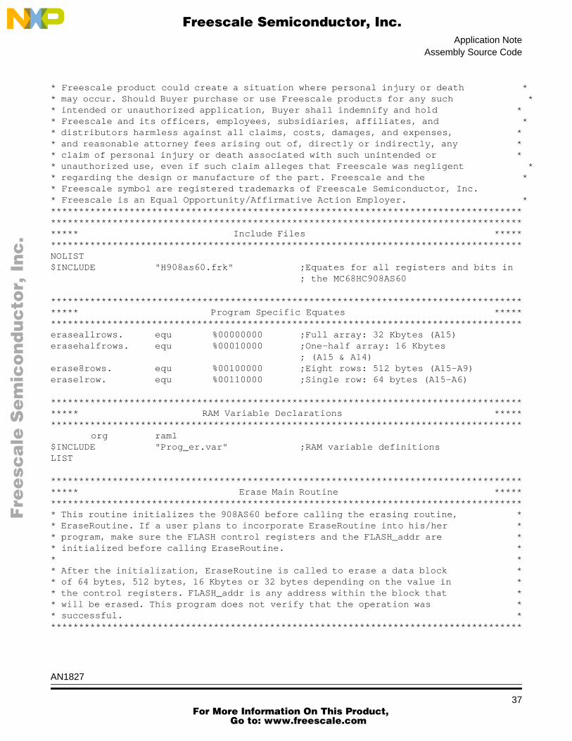
************************************************************************************************************************************************************************* ** Erase FLASH 2TS Memory on the MC68HC908AS60 ** ************************************************************************************** File Name: Erase.mrt Copyright (c) ** ** Current Revision: 1.0 ** Current Release Level: RP ** Current Revision Release Date: 9/6/99 ** ** Current Release Written By: Kim Sparks ** Freescale Systems Engineering - Austin, TX ** ** Assembled Under: CASM08 (P&E Micro Inc.) Ver.: 3.06 SLD ** ** Project Folder Name: FLASH_2TS ** ** Part Family Software Routine Works With: HC08 ** Part Module(s) Software Routine Works With: fls32k_a01 ** ** Routine Size (Bytes): 270 ** Stack Space Used (Bytes): 6 ** RAM Used (Bytes): 2 ** Global Variables Used: FLASH_addr ** Subroutine Called: EraseRoutine, WriteFLCR ** ** Full Functional Description Of Routine Design: ** Erase.mrt is the main routine that demonstrates how to erase different ** size blocks of FLASH 2TS memory on the MC68HC908AS60. ** ************************************************************************************** Freescale reserves the right to make changes without further notice to ** any product herein. Freescale makes no warranty, representation or ** guarantee regarding the suitability of its products for any particular ** purpose, nor does Freescale assume any liability arising out of the ** application or use of any product, circuit, and specifically disclaims ** any and all liability, including without limitation consequential or ** incidental damages. "Typical" parameters can and do vary in different ** applications. All operating parameters, including "Typicals" must be ** validated for each customer application by customer’s technical experts. ** Freescale does not convey any license under its patent rights nor the ** rights of others. Freescale products are not designed, intended, or ** authorized for use as components in systems intended for surgical ** implant into the body, or other applications intended to support or ** sustain life, or for any other application in which the failure of the *
AN1827
36 For More Information On This Product,
Go to: www.freescale.com
Application NoteAssembly Source Code
F
ree
sca
le S
em
ico
nd
uc
tor,
I
Freescale Semiconductor, Inc.n
c..
.
* Freescale product could create a situation where personal injury or death ** may occur. Should Buyer purchase or use Freescale products for any such ** intended or unauthorized application, Buyer shall indemnify and hold ** Freescale and its officers, employees, subsidiaries, affiliates, and ** distributors harmless against all claims, costs, damages, and expenses, ** and reasonable attorney fees arising out of, directly or indirectly, any ** claim of personal injury or death associated with such unintended or ** unauthorized use, even if such claim alleges that Freescale was negligent ** regarding the design or manufacture of the part. Freescale and the ** Freescale symbol are registered trademarks of Freescale Semiconductor, Inc. * Freescale is an Equal Opportunity/Affirmative Action Employer. ****************************************************************************************************************************************************************************** Include Files *****************************************************************************************NOLIST$INCLUDE "H908as60.frk" ;Equates for all registers and bits in
; the MC68HC908AS60
***************************************************************************************** Program Specific Equates *****************************************************************************************eraseallrows. equ %00000000 ;Full array: 32 Kbytes (A15)erasehalfrows. equ %00010000 ;One-half array: 16 Kbytes
; (A15 & A14)erase8rows. equ %00100000 ;Eight rows: 512 bytes (A15-A9)erase1row. equ %00110000 ;Single row: 64 bytes (A15-A6)
***************************************************************************************** RAM Variable Declarations *****************************************************************************************
org ram1$INCLUDE "Prog_er.var" ;RAM variable definitionsLIST
***************************************************************************************** Erase Main Routine ****************************************************************************************** This routine initializes the 908AS60 before calling the erasing routine, ** EraseRoutine. If a user plans to incorporate EraseRoutine into his/her ** program, make sure the FLASH control registers and the FLASH_addr are ** initialized before calling EraseRoutine. ** ** After the initialization, EraseRoutine is called to erase a data block ** of 64 bytes, 512 bytes, 16 Kbytes or 32 bytes depending on the value in ** the control registers. FLASH_addr is any address within the block that ** will be erased. This program does not verify that the operation was ** successful. *************************************************************************************
AN1827
37 For More Information On This Product,
Go to: www.freescale.com

Application Note
F
ree
sca
le S
em
ico
nd
uc
tor,
I
Freescale Semiconductor, Inc.n
c..
.
org flash-1
Start:mov #$71,config-1 ;Turn off the COP, but leave the LVI on
lda #$00 ;Set up the frequency divide controlsta flcr1 ; bits in flcr1 & flcr2 for ansta flcr2 ; appropriate charge pump clock
ldhx #$4001 ;Any address within the block that will; be erased
sthx FLASH_addr ;Set address of erase block
lda #eraseallrows. ;Set BLK1 and BLK0 in appropriatejsr WriteFLCR ; FLASH control register to specify the
; size of block to erase
jsr EraseRoutine ;Erase the block of FLASH including the; specified address
bra *
***************************************************************************************** Subroutine Body Includes Section *****************************************************************************************$INCLUDE "prog_er.srt" ;WriteFLCR and Delay subroutines
***************************************************************************************** Reset Vectors *****************************************************************************************
org resetfdb Start
************************************************************************************************************************************************************************* ** Program / Margin Read FLASH 2TS Memory on the MC68HC908AS60 ** ************************************************************************************** File Name: Program.mrt Copyright (c) ** ** Current Revision: 1.0 ** Current Release Level: RP ** Current Revision Release Date: 9/6/99 ** ** Current Release Written By: Kim Sparks ** Freescale Systems Engineering - Austin, TX ** ** Assembled Under: CASM08 (P&E Micro Inc.) Ver.: 3.06 SLD ** ** Project Folder Name: FLASH_2TS ** *
AN1827
38 For More Information On This Product,
Go to: www.freescale.com

Application NoteAssembly Source Code
F
ree
sca
le S
em
ico
nd
uc
tor,
I
Freescale Semiconductor, Inc.n
c..
.
* Part Family Software Routine Works With: HC08 ** Part Module(s) Software Routine Works With: fls32k_a01 ** ** Routine Size (Bytes): 278 ** Stack Space Used (Bytes): 5 ** RAM Used (Bytes): 11 ** Global Variables Used: FLASH_addr, data, attempt ** Subroutine Called: Prog8Bytes ** ** Full Functional Description Of Routine Design: ** Program.mrt is the main routine for the programming operation. It ** demonstrates a smart programming algorithm that minimizes the amount ** of time needed to program a page of FLASH 2TS memory on the ** MC68HC908AS60. One page consists of eight consecutive bytes of FLASH ** memory starting at either address $xxx0 or $xxx8. ** ****************************************************************************************** Include Files *****************************************************************************************NOLIST$INCLUDE "H908as60.frk" ;Equates for all registers and bits in
; the MC68HC908AS60org ram1
$INCLUDE "Prog_er.var" ;RAM variable definitionsLIST
***************************************************************************************** Program/Margin Read Main Routine ****************************************************************************************** This routine initializes the 908AS60 before calling the programming ** routine, Prog8Bytes. If a user plans to incorporate Prog8Bytes into ** his/her program, make sure the FLASH control registers, FLASH_addr and ** data buffer are initialized before calling Prog8Bytes. ** ** After the initialization, Prog8Bytes is called to program 8 data bytes, ** or one page of FLASH memory. If programming was successful, then the ** program will jump to the branch always statement in "No_Error." If ** programming failed, then the program will remain at the branch always ** statement in "Load." *************************************************************************************
org flash-2
Start:mov #$71,config-1 ;Turn off the COP, but leave the LVI on
lda #$00 ;Set up the frequency divide controlsta flcr1 ; bits in flcr1 & 2 for the appropriatesta flcr2 ; charge pump clock
ldhx #$8000 ;Load FLASH_addr with address of wheresthx FLASH_addr ; the 8 bytes should start being
AN1827
39 For More Information On This Product,
Go to: www.freescale.com

Application Note
*
F
ree
sca
le S
em
ico
nd
uc
tor,
I
Freescale Semiconductor, Inc.n
c..
.
; programmed. Must be XXX0 or XXX8
clrh ;Fill the RAM buffer, data, with valuesldx #8 ; to program into FLASH.
Load: stx data-1,X ; (ie. 01,02,03,04,05,06,07,08)decxbne Load
jsr Prog8Bytes ;Program the 8 data bytes
cbeqa #0,No_Error ;Check if a programming error occurred
bra * ; **Programming failed**; Take appropriate action
No_Error:bra * ; **Programming successful**
; End of program
***************************************************************************************** Subroutine Body Includes Section *****************************************************************************************$INCLUDE "prog_er.srt" ;Prog8Bytes, WriteFLCR and Delay
; subroutines***************************************************************************************** Vectors *****************************************************************************************
org resetfdb Start
************************************************************************************************************************************************************************* ** Programming and Erasing FLASH 2TS Memory on the MC68HC908AS60 ** ************************************************************************************** File Name: Prog_er.var Copyright (c) ** ** Current Revision: 1.0 ** Current Release Level: RP ** Current Revision Release Date: 9/6/99 ** ** Current Release Written By: Kim Sparks ** Freescale Systems Engineering - Austin, TX* ** Assembled Under: CASM08 (P&E Micro Inc.) Ver.: 3.06 SLD ** ** Project Folder Name: FLASH_2TS ** ** Part Family Software Routine Works With: HC08 ** ** RAM Used (Bytes): 11 ** *
AN1827
40 For More Information On This Product,
Go to: www.freescale.com

Application NoteAssembly Source Code
*
F
ree
sca
le S
em
ico
nd
uc
tor,
I
Freescale Semiconductor, Inc.n
c..
.
* Description: ** RAM variable definitions for Program.mrt and Erase.mrt ****************************************************************************************** RAM Variables *****************************************************************************************FLASH_addr rmb $2 ;16 bit Address of FLASH memory to
; erase or programdata: rmb $8 ;Eight data bytes that will be
; programmedattempt: rmb $1 ;Counts number of attempts to program
; a page************************************************************************************* ** Program / Margin Read and Erase FLASH 2TS Memory Subroutines ** ************************************************************************************** File Name: Prog_er.srt Copyright (c) ** ** Current Revision: 1.0 ** Current Release Level: RP ** Current Revision Release Date: 9/6/99 ** ** Current Release Written By: Kim Sparks ** Freescale Systems Engineering - Austin, TX* ** Assembled Under: CASM08 (P&E Micro Inc.) Ver.: 3.06 SLD ** ** Project Folder Name: FLASH_2TS ** ** Part Family Software Routine Works With: HC08 ** Part Module(s) Software Routine Works With: fls32k_a01 ** ** ** Module Size (Bytes): EraseRoutine 53 ** Prog8Bytes 160 ** WriteFLCR 20 ** Delay 9 ** Stack Space Used (Bytes): EraseRoutine 4 ** Prog8Bytes 3 ** WriteFLCR 0 ** Delay 1 ** RAM Used (Bytes): EraseRoutine 2 ** Prog8Bytes 11 ** WriteFLCR 0 ** Delay 0 ** Global Variable(s) Used: EraseRoutine FLASH_addr ** Prog8Bytes FLASH_addr, data, attempt ** WriteFLCR FLASH_addr ** Delay None ** Submodule(s) Called: EraseRoutine WriteFLCR, Delay ** Prog8Bytes WriteFLCR, Delay *
AN1827
41 For More Information On This Product,
Go to: www.freescale.com

Application Note
F
ree
sca
le S
em
ico
nd
uc
tor,
I
Freescale Semiconductor, Inc.n
c..
.
* WriteFLCR None ** Delay None ** Calling Sequence: JSR EraseRoutine, JSR Prog8Byte ** JSR WriteFLCR, JSR Delay ** Entry Label: EraseRoutine, Prog8Bytes, WriteFLCR ** Delay ** Entry Conditions: EraseRoutine 2 bytes address defined at ** FLASH_addr ** Prog8Bytes 2 bytes address defined at ** FLASH_addr ** 8 programming bytes located ** at variables data ** WriteFLCR 2 bytes address defined at ** FLASH_addr ** FLCR (FLASH Control ** Register) bit definition ** passed in accumulator ** Delay Delay variable passed in ** accumulator ** Number of Exit Points: 4 ** Exit Label: EraseRoutine Erase990 ** Prog8Bytes Prog990 ** WriteFLCR FLCR990 ** Delay Delay990 ** Exit Conditions: EraseRoutine None ** Prog8Bytes pass/fail result in ** accumulator ** WriteFLCR None ** Delay None ** ** Full Functional Description Of Subroutine: ** Prog_er.srt consists of two primary subroutines called EraseRoutine ** and Prog8Bytes. These demonstrate 2TS flash erasing and programming ** algorithms, respectively. The routines also call other subroutines ** WriteFLCR and Delay. ** ****************************************************************************************** FLASH Delay Equates ****************************************************************************************** Each delay time related to FLASH 2TS program and erase operations is ** calculated with bus speed 2.4576 MHz. *************************************************************************************tERASE: equ $F6 ;FLASH 2TS block/bulk erase time
; (~102 ms)tKILL: equ $0A ;FLASH 2TS high-voltage kill time
; (~209 µs)tHVD: equ $03 ;FLASH 2TS return to read time
; (~66 µs)tSTEP: equ $31 ;FLASH 2TS page program step size
; (~1 ms)tHVTV: equ $03 ;FLASH 2TS HVEN low to MARGIN high
AN1827
42 For More Information On This Product,
Go to: www.freescale.com

Application NoteAssembly Source Code
F
ree
sca
le S
em
ico
nd
uc
tor,
I
Freescale Semiconductor, Inc.n
c..
.
; time (~66 µs)tVTP: equ $08 ;FLASH 2TS MARGIN high to PGM low
; time (~168 µs)flsPULSES: equ $64 ;FLASH 2TS maximum page program pulses
; (100 pulses)***************************************************************************************** Erase a Block of FLASH Memory Subroutine ****************************************************************************************** This routine erases a block of FLASH of the size specified in the FLASH ** Control Registers and at the location specified by FLASH_addr. ** FLASH_addr is any address within the block to be erased. The routine ** follows the basic 9 step sequence of the FLASH erase operation. ** ** Initializations required: ** Set charge pump clock and block erase size in FLCR1 and FLCR2; ** FLASH_addr set ** Values returned: ** none *************************************************************************************EraseRoutine:
sei ;Disable interruptsldhx FLASH_addr ;Load the starting address of the block
; to be erased
lda #erase. ;Step 1 - Set the ERASE bitjsr WriteFLCR
lda flbpr1 ;Step 2 - Read from block protectlda flbpr2 ; registers
sta ,X ;Step 3 - Write to any FLASH address; within the block address range to be; erased with any data value;(indexed, 16 bit offset=H:X+$00)
lda #hven. ;Step 4 - Set the HVEN bitjsr WriteFLCR
lda #terase ;Step 5 - Wait for time tERASEpshxldx #$14
Again:jsr Delaydbnzx Againpulx
lda #hven. ;Step 6 - Clear the HVEN bitjsr WriteFLCR
lda #tkill ;Step 7 - Wait for time tKILLjsr Delay
AN1827
43 For More Information On This Product,
Go to: www.freescale.com

Application Note
F
ree
sca
le S
em
ico
nd
uc
tor,
I
Freescale Semiconductor, Inc.n
c..
.
lda #erase. ;Step 8 - Clear the ERASE bitjsr WriteFLCR
lda #thvd ;Step 9 - Wait for time tHVDjsr DELAY
cli ;Enable interrupts
Erase990:rts
***************************************************************************************** Program/Margin Read 8 Bytes of FLASH Memory Subroutine ****************************************************************************************** This routine programs the 8 bytes of data from the RAM data buffer to ** the FLASH memory starting at FLASH_addr. The programming is done in ** ascending order, ie. data[0] -> FLASH_addr[0], data[1] -> FLASH_addr[1], ** etc. ** ** The routine is structured into a loop for smart programming so that the ** minimum amount of high voltage is applied to the FLASH. Each time ** through the loop is called a "pulse." Each pulse consists of all 17 ** steps shown in the application note, with the programming time, tSTEP, ** equal to approximately 1 ms. ** ** If all 8 bytes program correctly in the approximately 1 ms time period, ** then the routine exits and returns control to the calling program. If ** the 8 bytes do not program correctly, another attempt(pulse) is made. ** This continues for the maximum number of pulses (flsPULSES). If the 8 ** bytes are not programmed successfully after a maximum number of pulses, ** then the programming error flag is incremented, the routine is exited ** and the error value (any non-zero value) is returned in the accumulator. ** ** Initializations required: ** Set charge pump clock in FLCR1 and FLCR2; FLASH_addr set; data ** buffer filled ** Values returned: ** A = Program Success/Error Flag *************************************************************************************Prog8Bytes:
sei ;No interrupts allowed during; programming
clr attempt ;Step 1 - Clear attempt counter
NextAttempt:ldhx FLASH_addr ;Load the address of the page to be
; programmed in the HX register
lda #pgm. ;Step 2 - Set the PGM bitjsr WriteFLCR
AN1827
44 For More Information On This Product,
Go to: www.freescale.com

Application NoteAssembly Source Code
F
ree
sca
le S
em
ico
nd
uc
tor,
I
Freescale Semiconductor, Inc.n
c..
.
lda flbpr1 ;Step 3 - Read from the block protectlda flbpr2 ; registers
lda data ;Step 4 - Copy the 8 bytes of datasta ,x ; from the RAM buffer to thelda data+1 ; appropriate FLASH locationssta 1,xlda data+2sta 2,xlda data+3sta 3,xlda data+4sta 4,xlda data+5sta 5,xlda data+6sta 6,xlda data+7sta 7,x
lda #hven. ;Step 5 - Set the HVEN bitjsr WriteFLCR
lda #tSTEP ;Step 6 - Wait for time tSTEPjsr Delay
lda #hven. ;Step 7 - Clear the HVEN bitjsr WriteFLCR
lda #tHVTV ;Step 8 - Wait for time tHVTVjsr Delay
lda #margin. ;Step 9 - Set the MARGIN bitjsr WriteFLCR
lda #tVTP ;Step 10 - Wait for time tVTPjsr Delay
lda #pgm. ;Step 11 - Clear the PGM bitjsr WriteFLCR
lda #tHVD ;Step 12 - Wait for time tHVDjsr Delay
lda ,x ;Step 13 and 14 - Check to see if thecmp data ; correct data was programmed in thebne Repeat ; FLASH page. If not, jump to Repeat tolda 1,x ; do another attempt. If so, jump tocmp data+1 ; Complete.bne Repeat
AN1827
45 For More Information On This Product,
Go to: www.freescale.com

Application Note
F
ree
sca
le S
em
ico
nd
uc
tor,
I
Freescale Semiconductor, Inc.n
c..
.
lda 2,xcmp data+2bne Repeatlda 3,xcmp data+3bne Repeatlda 4,xcmp data+4bne Repeatlda 5,xcmp data+5bne Repeatlda 6,xcmp data+6bne Repeatlda 7,xcmp data+7bne Repeatjmp Complete
Repeat:lda #margin. ; ** Program Failure **jsr WriteFLCR ;Step 15 - Clear the MARGIN bitinc attempt ;Step 16 - Increment attempt counterlda attempt
cbeqa #flsPULSES,Return ;Step 17 - If attempt is less thanjmp NextAttempt ; flsPULSES, go back to NextAttempt
; (Step 2)
Complete: ; ** Program Success **lda #margin. ;Clear the MARGIN bitjsr WriteFLCRclra
Return:cli ;Clear the interrupt mask bit and
; return
Prog990: ;If programming was unsuccessful inrts ; flsPULSES, the accumulator has a
; non-zero value
AN1827
46 For More Information On This Product,
Go to: www.freescale.com

Application NoteAssembly Source Code
F
ree
sca
le S
em
ico
nd
uc
tor,
I
Freescale Semiconductor, Inc.n
c..
.
***************************************************************************************** Write to a FLASH Control Register ****************************************************************************************** This routine determines whether flcr1 or flcr2 should be written to ** based on the FLASH address specified by FLASH_addr. ** ** ** Initializations required: ** H:X = FLASH_addr ** ** Values returned: ** None *************************************************************************************WriteFLCR:
cphx #flash-1 ;If FLASH_addr is in FLASH-1 array,bhs Array1 ; jump to Array1
eor flcr2 ;Write to flcr2 registersta flcr2bra FLCR990
Array1:eor flcr1 ;Write to flcr1 registersta flcr1
FLCR990:rts
***************************************************************************************** Delay Routine ****************************************************************************************** This routine delays for a variable amount of time depending on the value ** passed into the routine by the accumulator (A). ** Delay = (2 + (2 + 45 + 3) * A + 2 + 4) / Bus Freq ** ** Initializations required: ** A = delay variable ** Values returned: ** None *************************************************************************************Delay:
pshx ;2 cyc., Store the lower address of; FLASH_addr on the stack
Loop: ldx #$0F ;2 cyc., Initialize X for inner loop dbnzx * ;3 cyc., 15 * 3 = 45 cycles dbnza Loop ;3 cyc., Decrement value passed in by
; accumulator and repeat if necessary pulx ;2 cyc., Restore the lower address
Delay990: rts ;4 cyc., Return
AN1827
47 For More Information On This Product,
Go to: www.freescale.com

Application Note
*/
F
ree
sca
le S
em
ico
nd
uc
tor,
I
Freescale Semiconductor, Inc.n
c..
.
C Source Code
The sample assembly source code contained in the previous section iswritten in C language in this section.
In C, the main routines are called Er_mrt.c and Prog_mrt.c. The sameflowcharts apply.
/**********************************************************************************//**********************************************************************************//* *//* Erase FLASH 2TS Memory on the MC68HC908AS60 *//* *//**********************************************************************************//* File Name: Er_mrt.c Copyright (c) *//* *//* Current Revision: 1.0 *//* Current Release Level: RP *//* Current Revision Release Date: 10/02/99 *//* *//* Current Release Written By: Adeela Gill *//* Freescale Systems Engineering/* Austin, Texas *//* *//* Compiled Under: HiCross HC08 (HiWare) Ver.: 5.0.5 *//* *//* Project Folder Name: FLASH_2TS *//* *//* Part Family Software Routine Works With: HC08 *//* Part Module(s) Software Routine Works With: fls32k_a01 *//* *//* Routine Size (Bytes): 346 *//* Stack Space Used (Bytes): 9 *//* RAM Used (Bytes): 2 *//* Global Variables Used: FLASH_addr *//* Subroutine(s) Called: EraseRoutine, WriteFLCR *//* *//* Full Functional Description Of Routine Design: *//* Er_main.c is the main routine that demonstrates how to erase *//* different size blocks of FLASH 2TS memory on the MC68HC908AS60. *//* *//**********************************************************************************//* Freescale reserves the right to make changes without further notice to *//* any product herein. Freescale makes no warranty, representation or *//* guarantee regarding the suitability of its products for any particular *//* purpose, nor does Freescale assume any liability arising out of the *//* application or use of any product, circuit, and specifically disclaims *//* any and all liability, including without limitation consequential or */
AN1827
48 For More Information On This Product,
Go to: www.freescale.com

Application NoteC Source Code
/
F
ree
sca
le S
em
ico
nd
uc
tor,
I
Freescale Semiconductor, Inc.n
c..
.
/* incidental damages. "Typical" parameters can and do vary in different *//* applications. All operating parameters, including "Typicals" must be *//* validated for each customer application by customer’s technical *//* experts. Freescale does not convey any license under its patent rights *//* nor the rights of others. Freescale products are not designed, *//* intended, or authorized for use as components in systems intended for *//* surgical implant into the body, or other applications intended to *//* support or sustain life, or for any other application in which the *//* failure of the Freescale product could create a situation where *//* personal injury or death may occur. Should Buyer purchase or use *//* Freescale products for any such intended or unauthorized application, *//* Buyer shall indemnify and hold Freescale and its officers, employees, *//* subsidiaries, affiliates, and distributors harmless against all *//* claims, costs, damages, and expenses, and reasonable attorney fees *//* arising out of, directly or indirectly, any claim of personal injury *//* or death associated with such unintended or unauthorized use, even if *//* such claim alleges that Freescale was negligent regarding the design or *//* manufacture of the part. Freescale and the Freescale symbol are */* registered trademarks of Freescale Semiconductor, Inc. *//**********************************************************************************//**********************************************************************************//***** Include Files *****//**********************************************************************************/#include <as60_flash_frk.c> /* Equates for the registers and bits */
/* of the HC908AS60 that are used */#include <prog_er_var.c> /* RAM variable definitions *//**********************************************************************************//***** Program-Specific Defines *****//**********************************************************************************/#define eraseallrows 0x00 /* full array erase: 32 Kbytes */
/* cared addresses A15 */#define erasehalfrows 0x10 /* one-half array erase: 16 Kbytes */
/* cared addresses A15-A14 */#define erase8rows 0x20 /* eight row erase: 512 Bytes */
/* cared addresses A15-A9 */#define erase1row 0x30 /* single row erase: 64 Bytes */
/* cared addresses A15-A6 *//**********************************************************************************//***** Function Definitions *****//**********************************************************************************/extern void EraseRoutine (void);extern void writeFLCR (unsigned char);
/**********************************************************************************//***** Erase Main Routine *****//**********************************************************************************//* This routine initializes the 908AS60 before calling the erasing *//* routine, EraseRoutine. If a user plans to incorporate EraseRoutine *//* into his/her program, make sure the FLASH control registers and the *//* variable FLASH_addr are initialized before calling EraseRoutine. *//* After the initialization, EraseRoutine is called to erase a data */
AN1827
49 For More Information On This Product,
Go to: www.freescale.com

Application Note
F
ree
sca
le S
em
ico
nd
uc
tor,
I
Freescale Semiconductor, Inc.n
c..
.
/* block of 64 bytes, 512 bytes, 16 Kbytes or 32bytes depending on the *//* value in the control registers. FLASH_addr is any address within the *//* block that will be erased. This program does not verify that the *//* operation was successful. *//**********************************************************************************/void main (){
CONFIG1 = 0x71; /*Turn off the COP, but leave the *//* LVI on */
FLCR1 = 0x00; /*Set up the frequency divide */FLCR2 = 0x00; /* control bits in flcr1 & flcr2 */
/* for an appropriate charge pump *//* clock */
FLASH_addr=(unsigned char *)0x4001;/*Set address of erase block. This *//* is any address within the block *//* that will be erased */
writeFLCR(eraseallrows); /*Set BLK1 and BLK0 in appropriate *//* FLASH control register to specify *//* the size of block to erase */
EraseRoutine (); /*Erase the block of FLASH including *//* the specified address */
while (1);
}/**********************************************************************************//**** Subroutine Body Includes ****//**********************************************************************************/#include <prog_er_srt.c> /*Prog8Bytes, WriteFLCR and Delay */
/* Subroutines *//**********************************************************************************//**********************************************************************************//* *//* Program / Margin Read FLASH 2TS Memory on the MC68HC908AS60 *//* *//**********************************************************************************//* File Name: Prog_mrt.c Copyright (c) *//* *//* Current Revision: 1.0 *//* Current Release Level: RP *//* Current Revision Release Date: 10/02/99 *//* *//* Current Release Written By: Adeela Gill *//* Freescale Systems Engineering *//* Austin, Texas *//* *//* Compiled Under: HiCross HC08 (HiWare) Ver.: 5.0.5 *//* *//* Project Folder Name: FLASH_2TS *//* *//* Part Family Software Routine Works With: HC08 *//* Part Module(s) Software Routine Works With: fls32k_a01 */
AN1827
50 For More Information On This Product,
Go to: www.freescale.com

Application NoteC Source Code
F
ree
sca
le S
em
ico
nd
uc
tor,
I
Freescale Semiconductor, Inc.n
c..
.
/* *//* Routine Size (Bytes): 368 *//* Stack Space Used (Bytes): 12 *//* RAM Used (Bytes): 11 *//* Global Variables Used: FLASH_addr, data, attempt *//* Subroutine(s) Called: Prog8Bytes *//* *//* Full Functional Description Of Routine Design: *//* Prog_mrt.c is the main routine for the programming operation. It *//* demonstrates a smart programming algorithm that minimizes the *//* amount of time needed to program a page of 2TS FLASH memory on the *//* MC68HC908AS60. One page consists of eight consecutive bytes of *//* FLASH memory starting at either address $xxx0 or $xxx8. *//* *//**********************************************************************************//**********************************************************************************//***** Include Files *****//**********************************************************************************/#include <as60_flash_frk.c> /* Equates for the registers and bits */
/* of the HC908AS60 that are used */#include <prog_er_var.c> /* RAM variable definitions *//**********************************************************************************//***** Function Definitions *****//**********************************************************************************/extern void writeFLCR (unsigned char);extern unsigned char Prog8Bytes (void);/**********************************************************************************//***** Program/Margin Read Main Routine *****//**********************************************************************************//* This routine initializes the 908AS60 before calling the programming *//* routine, Prog8Bytes. If a user plans to incorporate Prog8Bytes into *//* his/her program, make sure the FLASH control registers, FLASH_addr *//* and data buffer are initialized before calling Prog8Bytes. *//* After the initialization, Prog8Bytes is called to program 8 data *//* bytes, or one page of FLASH memory. If programming was successful, *//* then the program will jump to the while(1) statement in the "if" *//* expression. If programming failed, then the program will remain at *//* the while(1) statement in the "else" expression. *//**********************************************************************************/void main (){
unsigned char count; /* Variable to count down bits */unsigned char pgmsuccess; /* Return value from Prog8Bytes */
CONFIG1 = 0x71; /*Turn off the COP, but leave the *//* LVI on */
FLCR1 = 0x00; /*Set up the frequency divide */FLCR2 = 0x00; /* control bits in flcr1 & 2 for */
/* the appropriate charge pump *//* clock */
AN1827
51 For More Information On This Product,
Go to: www.freescale.com

Application Note
*/
F
ree
sca
le S
em
ico
nd
uc
tor,
I
Freescale Semiconductor, Inc.n
c..
.
FLASH_addr = (unsigned char *)0x8000;/*Load FLASH_addr with address of *//* where the 8 bytes should start *//* being programmed. Must be XXX0 *//* or XXX8 */
for (count = 8; count != 0; count--) data[count-1]=count; /* Fill the RAM array, data, with */
/* values to program into FLASH. *//* (ie. 01,02,03,04,05,06,07,08) */
pgmsuccess=Prog8Bytes(); /* Program the 8 data bytes */
if (pgmsuccess!=0) /* Check if a programming error *//* occurred */
while (1); /* -- Programming failed -- *//* Take appropriate action */
else while (1); /* -- Programming successful -- *//* End of program */
}/**********************************************************************************//***** Subroutine Body Includes Section *****//**********************************************************************************/#include <prog_er_srt.c> /* Prog8Bytes, WriteFLCR and Delay */
/* Subroutines *//**********************************************************************************//**********************************************************************************//* *//* HC908AS60 FLASH Framework *//* *//**********************************************************************************//* File Name: as60_flash_frk.c Copyright (c) *//* *//* Current Revision: 1.0 *//* Current Release Level: RP *//* Current Revision Release Date: 10/02/99 *//* *//* Current Release Written By: Adeela Gill *//* Freescale Systems Engineering/* Austin, Texas *//* *//* Compiled Under: HiCross HC08 (HiWare) Ver.: 5.0.5 *//* *//* Project Folder Name: FLASH_2TS *//* *//* Part Family Software Routine Works With: HC08 *//* Part Module(s) Software Routine Works With: fls32k_a01 *//* *//* Framework Description: *//* This framework was generated using the MC68HC908AT60 General *//* Release Specification as a reference. *//**********************************************************************************/
AN1827
52 For More Information On This Product,
Go to: www.freescale.com

Application NoteC Source Code
*/
F
ree
sca
le S
em
ico
nd
uc
tor,
I
Freescale Semiconductor, Inc.n
c..
.
/**********************************************************************************//***** Register Equates *****//**********************************************************************************/#define CONFIG1 (*((volatile unsigned char *)0x001F))
/* Configuration Register 1 */
#define FLCR1 (*((volatile unsigned char *)0xFE0B))/* FLASH Control Register 1 */
#define FLCR2 (*((volatile unsigned char *)0xFE11))/* FLASH Control Register 2 */
#define FLBPR1 (*((volatile unsigned char *)0xFF80))/* FLASH Block Protect Register 1 */
#define FLBPR2 (*((volatile unsigned char *)0xFF81))/* FLASH Block Protect Register 2 */
#define FLASH1 (*((volatile unsigned char *)0x8000))/* Start Address of FLASH Array 1 */
#define FLASH2 (*((volatile unsigned char *)0x0450))/* Start Address of FLASH Array 2 */
/**********************************************************************************//***** Bit Equates *****//**********************************************************************************/#define HVEN 0x08 /* Bit 3: High-Voltage Enable Bit */#define MARGIN 0x04 /* Bit 2: Margin Read Control Bit */#define ERASE 0x02 /* Bit 1: Erase Control Bit */#define PGM 0x01 /* Bit 0: Program Control Bit *//**********************************************************************************//**********************************************************************************//* *//* Programming and Erasing FLASH 2TS Memory on the MC68HC908AS60 *//* *//**********************************************************************************//* File Name: Prog_er_var.c Copyright (c) *//* *//* Current Revision: 1.0 *//* Current Release Level: RP *//* Current Revision Release Date: 10/02/99 *//* *//* Current Release Written By: Adeela Gill *//* Freescale Systems Engineering/* Austin, Texas *//* *//* Compiled Under: HiCross HC08 (HiWare) Ver.: 5.0.5 *//* *//* Project Folder Name: FLASH_2TS *//* *//* Part Family Software Routine Works With: HC08 *//* Part Module(s) Software Routine Works With: fls32k_a01 *//* *//* RAM Used (Bytes): 11 *//* *//* Description: */
AN1827
53 For More Information On This Product,
Go to: www.freescale.com

Application Note
F
ree
sca
le S
em
ico
nd
uc
tor,
I
Freescale Semiconductor, Inc.n
c..
.
/* RAM variable definitions for Prog_mrt.c and Er_main.c *//* *//**********************************************************************************/
/**********************************************************************************//**** RAM Variables ****//**********************************************************************************/unsigned char * FLASH_addr; /* 16 bit address of FLASH memory to */
/* erase or program */unsigned char data[8]; /* Eight data bytes that will be */
/* programmed */unsigned char attempt; /* Counts number of attempts to */
/* program a page *//**********************************************************************************//**********************************************************************************//* *//* Program / Margin Read and Erase FLASH 2TS Memory Subroutines *//* *//**********************************************************************************//* File Name: Prog_er_srt.c Copyright (c) *//* *//* Current Revision: 1.0 *//* Current Release Level: RP *//* Current Revision Release Date: 10/02/99 *//* *//* Current Release Written By: Adeela Gill *//* Freescale Systems Engineering *//* Austin, Texas *//* *//* Compiled Under: HiCross HC08 (HiWare) Ver.: 5.0.5 *//* *//* Project Folder Name: FLASH_2TS *//* *//* Part Family Software Routine Works With: HC08 *//* Part Module(s) Software Routine Works With: fls32k_a01 *//* *//* Routine Sizes (Bytes): composite with called routines: *//* Prog8Bytes 187 bytes *//* EraseRoutine 75 bytes *//* Delay 24 bytes *//* WriteFLCR 30 bytes *//* Stack Space Used (Bytes): composite with called routines: *//* Prog8Bytes 8 bytes *//* EraseRoutine 9 bytes *//* Delay 2 bytes *//* WriteFLCR 1 bytes *//* RAM Used (Bytes): composite with called routines: *//* Prog8Bytes 11 bytes *//* EraseRoutine 2 bytes *//* Delay 0 bytes *//* WriteFLCR 2 bytes *//* *//* Global Variable(s) Used: Prog8Bytes FLASH_addr, data, attempt */
AN1827
54 For More Information On This Product,
Go to: www.freescale.com

Application NoteC Source Code
F
ree
sca
le S
em
ico
nd
uc
tor,
I
Freescale Semiconductor, Inc.n
c..
.
/* EraseRoutine FLASH_addr *//* Delay None *//* WriteFLCR FLASH_addr *//* *//* Submodule(s) Called: Prog8Bytes WriteFLCR, Delay *//* EraseRoutine WriteFLCR, Delay *//* Delay None *//* WriteFLCR None *//* *//* Calling Sequence: EraseRoutine () *//* int=Prog8Bytes () *//* WriteFLCR (unsigned char) *//* Delay (unsigned char) *//* *//* Entry Label: void EraseRoutine(), *//* unsigned char Prog8Bytes() *//* void WriteFLCR (unsigned char) *//* void Delay (unsigned char) *//* *//* Entry Conditions: EraseRoutine 2 byte address defined at *//* FLASH_addr *//* Prog8Bytes 2 bytes address defined at *//* FLASH_addr *//* 8 programming bytes located *//* at variable data *//* WriteFLCR 2 bytes address defined at *//* FLASH_addr *//* 1 byte FLCR bit definition *//* passed in *//* Delay 1 byte delay value passed in *//* *//* Number of Exit Points: 4 *//* Exit Label: EraseRoutine Erase990 *//* Prog8Bytes Prog990 *//* WriteFLCR FLCR990 *//* Delay Delay990 *//* *//* Exit Conditions: EraseRoutine None *//* Prog8Bytes pass/fail result returned *//* WriteFLCR None *//* Delay None *//* *//* Full Functional Description Of Subroutine: *//* Prog_er_srt.c consists of two primary subroutines called *//* EraseRoutine and Prog8Bytes. These demonstrate 2TS flash erasing *//* and programming algorithms, respectively. The routines also call *//* other subroutines WriteFLCR and Delay. *//* */
AN1827
55 For More Information On This Product,
Go to: www.freescale.com

Application Note
F
ree
sca
le S
em
ico
nd
uc
tor,
I
Freescale Semiconductor, Inc.n
c..
.
/**********************************************************************************//**********************************************************************************//***** FLASH Delay Equates *****//**********************************************************************************//* Each delay time related to FLASH 2TS program and erase operations is *//* calculated with bus speed 2.4576 MHz. *//**********************************************************************************/#define tERASE 0xF0 /* FLASH 2TS block/bulk erase time */
/* (~101 ms) */#define tKILL 0x0A /* FLASH 2TS high-voltage kill time */
/* (~210 µs) */#define tHVD 0x02 /* FLASH 2TS return to read time */
/* (~51 µs) */#define tSTEP 0x32 /* FLASH 2TS page program step size */
/* (~1 ms) */#define tHVTV 0x02 /* FLASH 2TS HVEN low to MARGIN high */
/* time (~51 µs) */#define tVTP 0x07 /* FLASH 2TS MARGIN high to PGM low */
/* time (~151 µs) */#define flsPULSES 0x64 /* FLASH 2TS maximum page program */
/* pulses (100 pulses) *//**********************************************************************************//***** Necessary Assembly-Level Commands Defines *****//**********************************************************************************/#define EnableInterrupts {asm CLI;}#define DisableInterrupts {asm SEI;}/**********************************************************************************//***** Function Initializations *****//**********************************************************************************/void EraseRoutine (void);unsigned char Prog8Bytes (void);void writeFLCR (unsigned char);void Delay (unsigned char);/**********************************************************************************//**** Erase a Block of FLASH Memory Subroutine *****//**********************************************************************************//* This routine erases a block of FLASH of the size specified in the *//* FLASH Control Registers and at the location specified by FLASH_addr. *//* FLASH_addr is any address within the block to be erased. The routine *//* follows the basic 9 step sequence of the FLASH erase operation. *//* *//* Initializations required: *//* Set charge pump clock and block erase size in FLCR1 and FLCR2; *//* FLASH_addr set *//* Values returned: *//* none *//**********************************************************************************/void EraseRoutine (){
unsigned char Blk_Protect1; /* set up local variables */unsigned char Blk_Protect2;unsigned char loop;
AN1827
56 For More Information On This Product,
Go to: www.freescale.com

Application NoteC Source Code
F
ree
sca
le S
em
ico
nd
uc
tor,
I
Freescale Semiconductor, Inc.n
c..
.
DisableInterrupts; /* Disable interrupts */
writeFLCR (ERASE); /* Step 1 - Set the ERASE bit */
Blk_Protect1 = FLBPR1; /* Step 2 - Read from the block */Blk_Protect2 = FLBPR2; /* protect registers */
*FLASH_addr = 0xFF; /* Step 3 - Write to any FLASH *//* address within the block address *//* range with any data value */
writeFLCR (HVEN); /* Step 4 - Set the HVEN bit */
for (loop=0x15; loop !=0; loop--) Delay (tERASE); /* Step 5 - Wait for time tERASE */
writeFLCR (HVEN); /* Step 6 - Clear the HVEN bit */
Delay (tKILL); /* Step 7 - Wait for time tKILL */
writeFLCR (ERASE); /* Step 8 - Clear the ERASE bit */
Delay (tHVD); /* Step 9 - Wait for time tHVD */
EnableInterrupts; /* Enable Interrupts */
Erase990:return;
}/**********************************************************************************//**** Program/Margin Read 8 Bytes of FLASH Memory Subroutine *****//**********************************************************************************//* This routine programs the 8 bytes of data from the RAM data array to *//* the FLASH memory starting at FLASH_addr. The programming is done in *//* ascending order, ie. data[0] -> FLASH_addr[0], data[1] -> *//* FLASH_addr[1], etc. *//* *//* The routine is structured into a loop for smart programming so that *//* the minimum amount of high voltage is applied to the FLASH. Each time *//* through the loop is called a "pulse". Each pulse consists of all 17 *//* steps shown in the application note, with the programming time, tSTEP, *//* equal to approximately 1 ms. *//* *//* If all 8 bytes program correctly in the approximately 1ms time period, *//* then the routine exits and returns control to the calling program. If *//* the 8 bytes do not program correctly, another attempt(pulse) is made. *//* This continues for the maximum number of pulses (flsPULSES). If the 8 *//* bytes are not programmed successfully after a maximum number of *//* pulses, then the programming error flag is incremented, the routine is *//* exited and the error value (any non-zero value) is returned. *//* */
AN1827
57 For More Information On This Product,
Go to: www.freescale.com
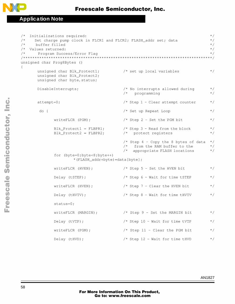
Application Note
F
ree
sca
le S
em
ico
nd
uc
tor,
I
Freescale Semiconductor, Inc.n
c..
.
/* Initializations required: *//* Set charge pump clock in FLCR1 and FLCR2; FLASH_addr set; data *//* buffer filled *//* Values returned: *//* Program Success/Error Flag *//**********************************************************************************/unsigned char Prog8Bytes (){
unsigned char Blk_Protect1; /* set up local variables */unsigned char Blk_Protect2;unsigned char byte,status;
DisableInterrupts; /* No interrupts allowed during *//* programming */
attempt=0; /* Step 1 - Clear attempt counter */
do { /* Set up Repeat Loop */
writeFLCR (PGM); /* Step 2 - Set the PGM bit */
Blk_Protect1 = FLBPR1; /* Step 3 - Read from the block */Blk_Protect2 = FLBPR2; /* protect registers */
/* Step 4 - Copy the 8 bytes of data *//* from the RAM buffer to the *//* appropriate FLASH locations */
for (byte=0;byte<8;byte++)*(FLASH_addr+byte)=data[byte];
writeFLCR (HVEN); /* Step 5 - Set the HVEN bit */
Delay (tSTEP); /* Step 6 - Wait for time tSTEP */
writeFLCR (HVEN); /* Step 7 - Clear the HVEN bit */
Delay (tHVTV); /* Step 8 - Wait for time tHVTV */
status=0;
writeFLCR (MARGIN); /* Step 9 - Set the MARGIN bit */
Delay (tVTP); /* Step 10 - Wait for time tVTP */
writeFLCR (PGM); /* Step 11 - Clear the PGM bit */
Delay (tHVD); /* Step 12 - Wait for time tHVD */
AN1827
58 For More Information On This Product,
Go to: www.freescale.com

Application NoteC Source Code
F
ree
sca
le S
em
ico
nd
uc
tor,
I
Freescale Semiconductor, Inc.n
c..
.
for (byte=0; byte<8; byte++)if (*(FLASH_addr+byte) == data[byte]) status++;
/* Step 13 and 14 - Check to see if *//* the correct data was programmed *//* in the FLASH page. If not, *//* proceed with the bracketed *//* expressions. If so, skip to next *//* if statement. */
if (status != 8) {/* -- Program Failure -- *//* Step 15 - Clear the MARGIN bit */
writeFLCR (MARGIN);attempt++; /* Step 16 - Increment attempt */
/* counter */ }
if (status == 8) /* -- Program Success -- */writeFLCR (MARGIN);
/* Clear the MARGIN bit */
} while ((status!=8) && (attempt<flsPULSES));/* Step 17 - If attempt is less than *//* flsPULSES, go back to step 2 */
EnableInterrupts; /* Clear the interrupt mask bit */
Prog990:return (8-status); /* If programming was unsuccessful in */
/* flsPULSES, a non-zero value is *//* returned */
}/**********************************************************************************//**** Write to a FLASH Control Register *****//**********************************************************************************//* This routine determines whether flcr1 or flcr2 should be written to *//* based on the FLASH address specified by FLASH_addr. *//* *//* Initializations required: *//* set FLASH_addr *//* Values returned: *//* None *//**********************************************************************************/void writeFLCR (unsigned char A){
/* FLASH-1=$8000, FLASH-2=$0450 */if (FLASH_addr >= &FLASH1) /*If FLASH_addr is in FLASH-1 array */
FLCR1 = FLCR1 ^ A; /* write to FLCR1 Register */
elseFLCR2 = FLCR2 ^ A; /* else write to FLCR2 Register */
FLCR990:return;
AN1827
59 For More Information On This Product,
Go to: www.freescale.com

N
ON
-D
IS
CL
OS
UR
E
AG
RE
EM
EN
T
RE
QU
IR
ED
Application Note
F
ree
sca
le S
em
ico
nd
uc
tor,
I
Freescale Semiconductor, Inc.n
c..
.
/**********************************************************************************//**** Delay Routine *****//**********************************************************************************//* This routine delays for a variable amount of time depending on the *//* value passed into the routine as variable A. *//* Delay time = (12 + (5 + (11+72+11)*A + 11) + 8) / Bus Freq *//* This equation includes the bus cycles from calling the delay routine *//* until hitting the next line of code. This allows the user to *//* accurately predict the delay between two steps in the code. *//* *//* Initializations required: *//* Pass in variable A = Delay Value *//* Values returned: *//* None *//**********************************************************************************/void Delay (unsigned char A){
unsigned char count;
while (A!=0) {for (count=0x03;count!=0;count--);A--;
}
Delay990:return;
}
For More Information On This Product,
Go to: www.freescale.com