an1124: embedded acpi compliant ddr power generation using ... · embedded acpi compliant ddr power...
TRANSCRIPT

Embedded ACPI Compliant DDR Power Generation Using the ISL6537A and ISL6506
APPLICATION NOTE
AN1124Rev 0.00
January 15, 2007
IntroductionThe ISL6537A, in conjunction with the ISL6506, provides a complete ACPI compliant power solution for computer systems with either dual channel DDRI, DDRII, or DDRIII Memory systems. The chipset offered by Intersil provides the necessary control, protection and proper ACPI sequencing of the following rails: 5VDUAL, 3.3VDUAL, VDDQ_DDR, VTT_DDR, VREF_DDR, VDAC, VGMCH, and VTT_GMCH/CPU.
The ISL6537A consists of a synchronous buck controller to supply VDDQ_DDR with high current during S0/S1 (Run) states and standby current during S3 (Suspend-To-RAM = STR) state. During Run mode, a fully integrated sink-source regulator generates an accurate (VDDQ_DDR/2) high current VTT_DDR voltage. A buffered version of the VDDQ_DDR/2 reference is provided as VREF_DDR. The ISL6537A also features a PWM controller that, in conjunction with an external gate driver IC, regulates VGMCH and two LDO controllers to regulate VDAC and VTT_GMCH/CPU. A more complete description of the ISL6537A can be found in the datasheet[1].
The ISL6506 controls the 5VDUAL and 3.3VDUAL rails. There are three versions of the ISL6506. The version required will depend on whether 5VDUAL is required to be active during S4/S5. A more complete description of the ISL6506 can be found in the datasheet[2].
Quick Start EvaluationThe ISL6537A_6506EVAL1Z board is shipped ‘ready to use’ right from the box. The ISL6537A_6506EVAL1Z supports testing with an ATX power supply. All seven outputs can be exercised through external loads. Both the VDDQ and VTT regulators have the ability to source or sink current while all other outputs may only source current.
There are posts available on each regulated output rail for drawing a load and/or monitoring the voltages. Eighteen individually labeled probe points are also available for use. These probe points provide Kelvin connections to signals which may be of interest to the designer.
Two switches have been placed on the board to accommodate ACPI signal simulation. These two switches generate the SLP_S3 and SLP_S5 signals that are sent to the ISL6506, ISL6537A and the ATX.
Recommended Test Equipment
To test the full functionality of the ISL6537A and ISL6506, the following equipment is recommended:
• An ATX power supply (minimum 160W configuration)• Multiple electronic loads• Four channel oscilloscope with probes• Precision digital multimeters
As there are seven regulated rails, it is difficult to exercise and monitor all of them at the same time. The user may wish to employ discrete resistive loads in addition to electronic loads. Electronic loads are favored because they allow the user to apply a multitude of varying load levels and load transients which allow for a broader analysis.
Circuit Setup
SET SWITCHES
Ensure that the S3 switch is in the ACTIVE position and the S5 switch is in the S5 position. With the switches in these positions, the board will be forced into a sleep state at initial power up.
CONNECT THE ATX SUPPLY
Plug the 20-pin connector from the ATX power supply into the 20-pin receptacle, J1, on the evaluation board. Should the ATX power supply have a master AC switch, turn this switch to the OFF position prior to applying AC voltage.
CONNECT LOADS
Figure 1 details the locations of the available power, ground, and signal connection points on the ISL6537A_6506EVAL1Z evaluation board. The maximum loads specified for each rail below are absolute. VTT_DDR is cascaded from the VDDQ_DDR rail while the VTT_GMCH/CPU is cascaded from the VGMCH rail (refer to “ISL6537A_6506EVAL1Z Schematic” on page 10). Any loading of a cascaded rail will itself be a load on the rail that is providing input and must be accounted for prior to application of loads.
FIGURE 1. ISL6537A_6506EVAL1Z BOARD POWER AND SIGNAL CONNECTIONS
KEY - Ground Terminal for Load and/or Probe Ground Clip
- Output Rail Terminal for Load and/or Probe
- Probe Point
ATXCONNECTOR
(VDDQ)
ISL6506
(DDR_VTT)
(VGMCH)
(VTT_GMCH/CPU)
ISL6537A
(5VDUAL)
(3VDUAL)
S3 S5
(SWITCHES)
ISL6537A_6506EVAL1Z
(VDAC)
SLP_S3# VCC5 5VDUAL UGATE
12V VREF_IN
VCC3 5VSBY VID_PG LGATE
SLP_S5# PWR_OK VREF_OUT
3VDUAL
AN1124 Rev 0.00 Page 1 of 15January 15, 2007

Embedded ACPI Compliant DDR Power
Generation Using the ISL6537A and ISL6506
Loading VDDQ_DDR - Sourcing Current: Connect the positive terminal of an electronic load to the VDDQ post. Connect the return terminal of the same load to the corresponding GND post. The maximum load current that the rail will support prior to entering an overcurrent condition is 15A.
Loading VDDQ_DDR - Sinking Current: Typically, the VDDQ rail does not sink current, however, the ISL6537A has the ability to allow the VDDQ rail to do just that. To test the VDDQ rail while sinking current, connect the positive terminal of an electronic load to the 5VDUAL post. Connect the return terminal of the same load to the VDDQ post. The maximum load current that the rail will support prior to entering an overcurrent condition is 15A.
CAUTION: The return terminal of the load must float for this to work properly.
Loading VTT_DDR - Sourcing Current: To test VTT_DDR while the regulator sources current, connect the positive terminal of an electronic load to the DDR_ VTT post. Connect the return terminal of the same load to the corresponding GND post. The maximum continuous current that the rail will support is 2A. Transient loads to 3A are also supported.
Loading VTT_DDR - Sinking Current: To test VTT_DDR while the regulator sinks current, connect the positive terminal of an electronic load to the VDDQ post. Connect the return terminal of the same load to the DDR_VTT post. The maximum continuous current that the rail will support is 2A. Transient loads to 3A are also supported.
CAUTION: The return terminal of the load must float for this to work properly.
Loading VGMCH: Connect the positive terminal of an electronic load to the VGMCH post. Connect the return terminal of the corresponding GND post. The maximum load supported by this rail is 10A.
Loading VDAC: Connect the positive terminal of an electronic load to the VDAC post. Connect the return terminal of the corresponding GND post. The maximum load supported by this rail is 5A.
Loading VTT_GMCH/CPU - Sourcing Current: Connect the positive terminal an electronic load to the VTT_GMCH/CPU post. Connect the return terminal of the corresponding GND post. The maximum load supported by this rail is 5A.
Loading 5VDUAL: Connect the positive terminal of an electronic load to the 5VDUAL post. Connect the return terminal of the corresponding GND post. The maximum load supported by this rail is 14A.
Loading 3VDUAL: Connect the positive terminal of an electronic load to the 3VDUAL post. Connect the return terminal of the corresponding GND post. The maximum load supported by this rail is 14A.
Operation
APPLY POWER TO THE BOARD
Plug the ATX supply into the mains. If the supply has an AC switch, turn it on. With the S3 and S5 switches in the ACTIVE and S5 positions, respectively, the board will be in the S5 sleep state. Voltages present on the board will be 5VSBY which is supplied by the ATX and 3VDUAL which is controlled by the ISL6506.
To enable the circuit, toggle the S5 switch to ACTIVE. This will place the board in the S0 state. All outputs should be brought up.
EXAMINE START-UP WAVEFORMS AND OUTPUT QUALITY UNDER VARYING LOADS
Start-up is immediate following the transition to the S0 state. Using an oscilloscope or other laboratory equipment, the ramp-up and/or regulation of the outputs can be studied. Loading of the output can be accomplished through the use of an electronic load. Other methods, such as the use of discrete power resistors will work for loading as well.
Reference Design
General
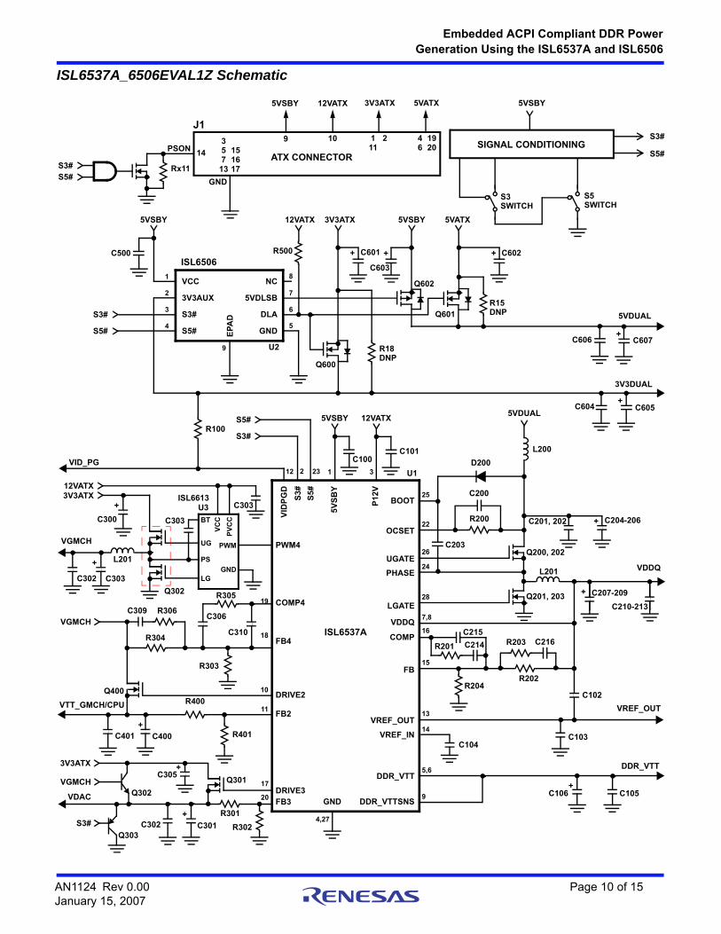
The ISL6537A_6506EVAL1Z is an evaluation board that highlights the operation of the ISL6537A and ISL6506 in an embedded ACPI and DDR DRAM Memory Power application. The VDDQ_DDR supply has been designed to supply 1.8V at a maximum load of 15A. The VTT_DDR termination supply will track the VDDQ_DDR supply at 50% while sourcing or sinking current. The second PWM controller is designed to supply up to 10A of current at 1.5V for VGMCH while the single stage LDOs supply 2.5V for VDAC and 1.2V for VTT_GMCH/CPU.Refer to “ISL6537A_6506EVAL1Z Schematic” on page 10, “ISL6537A_6506EVAL1Z Bill of Material” on page 11 and “ISL6537A_6506EVAL1Z Layout” on page 12).
Power Up And State Transitions
Sleep State Transitions
There are several distinct state transitions that the ISL6537A and ISL6506 support. These include a Cold/Mechanical Start (S5 to S0 state transition), Active to Sleep (S0 to S3 transition), Sleep to Active (S3 to S0 transition) and finally Active to Shutdown (S0 to S5 transition). Table 1 shows the switch positions and the corresponding ACPI states.
TABLE 1. ISL6537A_6506EVAL1Z STATES
S3 SWITCH S5 SWITCH SLEEP STATE ATX STATE
ACTIVE ACTIVE S0 (Active) ON
S3 ACTIVE S3 Standby
ACTIVE S5 S5 Standby
S3 S5 S5 Standby
AN1124 Rev 0.00 Page 2 of 15January 15, 2007
Embedded ACPI Compliant DDR Power
Generation Using the ISL6537A and ISL6506
If both the S3 and S5 switches are thrown to S3 and S5, respectively, the board will default to an S5 state. If the board is in either an S3 or S5 sleep state, the ATX supply is put into standby mode, where only the 5VSBY rail is active.
Initial Power Up - Cold Start
If both the S3 and S5 switches are toggled to the ACTIVE position prior to applying AC power to the ATX supply, the board will immediately enter into S0 state when the 5VSBY rail comes up after the AC power is applied to the ATX. Figure 2 shows a Cold Start. Examination of the VDAC
waveform shows this rail ramping up with the VGMCH rail. This is due to an external circuit that was included on the evaluation board and is described in the section titled “Grantsdale VDAC Sequencing Circuitry” on page 5.
S5 Sleep State to S0 State Transition
If the S5 switch is toggled to the S5 position prior to application of AC power to the ATX supply, then the board will immediately enter into the S5 sleep state when the 5VSBY rail comes up after the AC voltage is applied to the ATX. The ISL6506 will bring up the 3VDUAL rail but all other output rails will be inactive. The transition from the S5 state to the S0 state will occur when the S5 switch is toggled to theACTIVE position. Figure 3 shows this transition. Note that the 3VDUAL rail are already active prior to the other rails soft starting. If the ISL6506A had been used, the 5VDUAL rail would have been active in the S5 state as well. During testing of the evaluation board, it may be observed that the 5VDUAL rail stays up during the S5 sleep state. If this behavior is observed, the explanation would be that the bulk capacitor on the 5VDUALrail did not discharge a significant amount while the board was in the S5 sleep state.
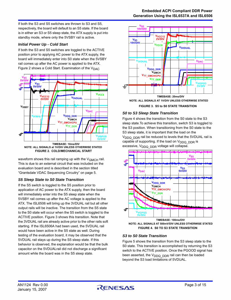
S0 to S3 Sleep State Transition
Figure 4 shows the transition from the S0 state to the S3 sleep state.To achieve this transition, switch S3 is toggled to the S3 position. When transitioning from the S0 state to the S3 sleep state, it is important that the load on the VDDQ_DDR rail be reduced to levels that the 5VDUAL rail is capable of supporting. If the load on VDDQ_DDR is excessive, VDDQ_DDR voltage will collapse.
S3 to S0 State Transition
Figure 5 shows the transition from the S3 sleep state to the S0 state. This transition is accomplished by returning the S3 switch to the ACTIVE position. Once the PGOOD signal has been asserted, the VDDQ_DDR rail can then be loaded beyond the S3 load limitations of 5VDUAL.
FIGURE 2. COLD/MECHANICAL START
TIMEBASE: 10ms/DIVNOTE: ALL SIGNALS at 1V/DIV UNLESS OTHERWISE STATED
VS55V/DIV
VS35V/DIV
VVIDPGD5V/DIV
VVCC5V5VDUAL
V3VDUAL
V5SBY
VDDQ_DDRVGMCH
VTT_GMCH/CPUVTT_DDR
VVCC122V/DIV
VDAC
FIGURE 3. S5 to S0 STATE TRANSITION
VS510V/DIV
VS310V/DIV
VVIDPGD5V/DIV
VVCC5V5VDUAL
V3VDUAL
VVCC122V/DIV
TIMEBASE: 20ms/DIV
NOTE: ALL SIGNALS AT 1V/DIV UNLESS OTHERWISE STATED
VDDQ_DDRVGMCH
VTT_GMCH/CPUVTT_DDR
VDAC
FIGURE 4. S0 TO S3 STATE TRANSITION
VS55V/DIV
VS35V/DIV
VVIDPGD5V/DIV
VDDQ_DDRVGMCHVTT_GMCH/CPUVTT_DDR
VDAC
TIMEBASE: 100ms/DIV
NOTE: ALL SIGNALS AT 500mV/DIV UNLESS OTHERWISE STATED
AN1124 Rev 0.00 Page 3 of 15January 15, 2007

Embedded ACPI Compliant DDR Power
Generation Using the ISL6537A and ISL6506
ACPI Start-up Timing
The ISL6506 and ISL6537A chipset were designed to work in tandem to Start-up critical ACPI and Memory voltages within a specific window of opportunity during the overall Start-up or sleep recovery process of a typical motherboard. Figure 6 shows a generic desktop sleep state to wake state sequencing. At time T1, either the SLP_S3# or SLP_S5#
signal transitions HIGH, which is the signal to the system to enter into the S0 state. At time T2, 10ns later, PS_ON, the signal that commands the ATX supply to turn on, is forced LOW. At time T3, the ATX rails have risen to 95% of their targeted nominal levels. The time between T2 and T3 can be between 100ms and 500ms. At time T4, the PWR_OK signal from the ATX supply starts to rise. The time between T3 and T4 will also fall between 100ms and 500ms. At time T5, the ATX PWR_OK signal has risen HIGH. This transition is specified to be less than 10ms. At this point, the PWROK signal from the GMCH is commanded HIGH. At time T6, anywhere from 31 to 44 RTCs after PWROK has asserted HIGH, the PCIRST# signal from the ICH asserts HIGH.
When PCIRST# asserts HIGH, bus traffic resumes and the system is awake.
The ISL6506 and ISL6537A chipset bring all the ACPI rails under their control into regulation between time T3 and T4. This timing assures, even with minimum specified system timings, that the regulators will have their inputs available from the ATX supply and also that the output rails will be in regulation and ready for bus traffic once PCIRST# asserts HIGH.[4][5]
Evaluation Board DesignThe complete Bill of Material for the evaluation board can be seen in “ISL6537A_6506EVAL1Z Bill of Material” on page 11. This section gives an overview of the design parameters and decisions made for each regulator.
ISL6506 Circuitry
The ISL6506 incorporates all the ACPI timing, control and monitoring required for the 5VDUAL and 3.3VDUAL rails, while maintaining a low component count. The Vishay Si7840 was utilized for both N-Channel MOSFET pass elements due to the low rDS(ON) and thermal capabilities of the packaging. Very little power is dissipated from the MOSFET in this application. The P-Channel MOSFET, the Vishay Si7483, was chosen for similar reasons.
The MOSFET thermal capabilities and it’s rDS(ON) are the two major considerations when choosing a MOSFET as a pass element for the 5VDUAL and 3.3VDUAL rails. The maximum allowable temperature rise of the MOSFET is used to calculate the maximum power that the MOSFET can dissipate via the thermal resistance ratings of the FET. The maximum rDS(ON) of the MOSFET can then be calculated by dividing the maximum allowable power dissipation of the MOSFET by the square of the maximum load current that will flow through the MOSFET. If the datasheet specified rDS(ON) of the MOSFET being considered is less than this calculated maximum rDS(ON) value, then the MOSFET can be used safely in the application, provided proper layout techniques for thermal dissipation are used.
ISL6537A Circuitry
VDDQ_DDR Switching Regulator
The VDDQ_DDR switching regulator was designed to handle a 15A continuous output load while maintaining 1.8V. Voltage excursions due to transient loading of 25A/µs were to be no greater than 50mV with a full 15A load step.
In order to supply 15A of continuous current, two upper and two lower MOSFETs were utilized. The part chosen for both upper and lower MOSFETs was the Vishay Si7840BDP. The choice of both the MOSFET and the parallel MOSFET configuration will actually allow for a continuous current of at least 20A without the FETs becoming too hot.
The transient specifications were met by employing large value capacitors that have relatively low ESR ratings and by
FIGURE 5. S3 TO S0 STATE TRANSITION
TIMEBASE: 20ms/DIV
NOTE: ALL SIGNALS AT 500mV/DIV UNLESS OTHERWISE STATED
VS55V/DIV
VS35V/DIV
VVIDPGD5V/DIV
VDDQ_DDRVGMCHVTT_GMCH/CPUVTT_DDR
VDAC
FIGURE 6. GENERIC WAKEUP SEQUENCING
SLP_S3#
PS_ON
PWR_OK
PWROK
PCIRST#
+12V, 5V,
SLP_S5#OR
T1 T2 T3 T4 T5T6
3.3V
(NOT TO SCALE)
AN1124 Rev 0.00 Page 4 of 15January 15, 2007

Embedded ACPI Compliant DDR Power
Generation Using the ISL6537A and ISL6506
using some ceramic capacitors to decrease the effective ESR even more. Three 1800µF bulk capacitors with 16m ESR were utilized as the bulk output capacitance. During a transient, the large capacitance supplies energy to the load while the output inductor current slews up to match the load current.
The output inductor was designed so that the ripple voltage on the output rail would be approximately 20mV. A simple wirewound toroidal inductor was designed for this regulator. To save on the Bill of Material (BoM) cost, the same inductor was used on the input filter to the VDDQ regulator.
Since there is an input inductor, the input capacitors must be rated to handle all of the AC RMS current going through the upper MOSFET. The capacitors that were chosen have RMS current ratings that exceed the maximum RMS current expected at full load.
The final aspect to the VDDQ_DDR regulator design was to insure the stability of the system. A Type III compensation network was chosen for this design. The compensation components were calculated to give a system bandwidth of about 50kHz with a Phase Margin of approximately 65°. For more information on calculating the compensation components for a single phase buck regulator, see Intersil’s Technical Brief, TB417, titled “Designing Stable Compensation Networks for Single Phase Voltage Mode Buck Regulators.”[3]
VGMCH SWITCHING REGULATOR
The regulation of the VGMCH rail is accomplished by down converting from the 3.3VATX rail with a switching regulator. The ISL6537A incorporates all the control aspects of the switching regulator and requires that a MOSFET gate driver be utilized to drive the upper and lower MOSFETs of the synchronous buck switching regulator. This design utilizes the ISL6613 to drive the switching MOSFETs. The MOSFETs chosen were dual packaged FETs from Vishay, the Si7844. The FETs and the package allow for efficient regulation at full load of 10A. The output inductor is the same as the input and output inductor used in the VDDQ regulator. The output capacitor allows for a large amount of capacitance while minimizing the output ripple to less than 40mV. The compensation network is a Type III. This network yields a stable system with approximately 30kHz of bandwidth.
LDO REGULATORS
The VTT_DDR regulator required minimal design work as the control circuitry and pass element are incorporated within the ISL6537A. Except for the pass element and output capacitance, all other circuitry for the remaining LDOs is also contained within the ISL6537A.
The VDAC and VTT_GMCH/CPU are both regulated via the internal LDO controllers. The pass elements chosen for both was the Vishay Si7840BDP. This allowed for a higher single
part count on the BoM while allowing the regulators to source a sufficient amount of load.
For all the LDOs, including the VTT_DDR regulator, the output capacitance was chosen to maintain a stable output rail while minimizing voltage excursions due to load transients.
GRANTSDALE VDAC SEQUENCING CIRCUITRY
The Grantsdale chipset imposes special requirements on the startup and shutdown timing of the VDAC rail in relation to the VGMCH rail. During Start-up, the VDAC rail must not Start-up until the VGMCH rail has reached at least 0.7V. When entering a sleep state, the VDAC rail must be brought below the VGMCH rail level before the VGMCH rail can begin to ramp down.
A circuit was included on the ISL6537A evaluation board that will keep a 0.7V differential between the VGMCH and VDAC rails until the VDAC rail is soft started. This circuit will also discharge the VDAC rail immediately upon entering into a sleep state. This circuit is shown in Figure 7. During Start-up, the base-emitter junction of Q302 maintains a 0.7V differential between VGMCH and VDAC. Upon assertion of the SLP_S3# signal, Q303 discharges the VDAC rail which allows the VGMCH rail to discharge.
Evaluation Board PerformanceThis section presents the performance of the ISL6537A_6506EVAL1Z evaluation board while subjected to various conditions.
Switching Regulator Ripple Voltages
Figure 8 shows the ripple voltage on the VDDQ and VGMCH outputs.
FIGURE 7. GRANTSDALE SEQUENCING CIRCUITRY
3V3ATX
VGMCH
SLP_S3#
Q302
Q303
VDAC
AN1124 Rev 0.00 Page 5 of 15January 15, 2007

Embedded ACPI Compliant DDR Power
Generation Using the ISL6537A and ISL6506
Transient Performance
Figures 9 through 14 show the response of the outputs when subjected to a variety of transient loads while in the Active (S0) State. Figure 9 shows VDDQ_DDR under transient
loading. The response of the VDDQ_DDR regulator to the transient load brings the output voltage back into regulation very quickly.
Figure 10 shows VTT_DDR under a transient loading that causes VTT_DDR to source current.
While the load is being applied to the VTT_DDR rail, there is a noticeable reaction in the VDDQ_DDR rail as well. Since the VTT_DDR rail is derived from the VDDQ_DDR rail, any load on the VTT_DDR rail is seen by the VDDQ_DDR rail.
Figure 11 shows VTT_DDR under a transient that causes VTT_DDR to sink current.
Again, the reaction of the VDDQ_DDR rail is evident since the loading on the VTT_DDR rail is transferred directly to the VDDQ_DDR rail. In both cases, sourcing and sinking current, where the VTT_DDR rail has been loaded and the VDDQ_DDR rail has responded to the loading, the VTT_DDR rail did not appear to be affected as much as the VDDQ_DDR rail. This is because a linear regulator (VTT_DDR) will respond much faster than a switching regulator (VDDQ_DDR). This difference in response is because the
TIMEBASE: 1ms/DIV
VDDQ_DDR20mV/DIV AC COUPLED
FIGURE 8. VDDQ and VGMCH RIPPLE VOLTAGE
VUGATE(DDQ)10V/DIVVGMCH
50mV/DIV AC COUPLED
VUGATE(GMCH)10V/DIV
FIGURE 9. TRANSIENT ON VDDQ
VDDQ_DDR (1.8V OFFSET)
TIMEBASE: 200ms/DIV
NOTE: ALL SIGNALS AT 50mV/DIV UNLESS OTHERWISE STATED
ILOAD10A/DIV
VTT (0.9V OFFSET)
VGMCH (1.5V OFFSET)
VTT_GMCH/CPU (1.2V OFFSET)
VDAC (2.5V OFFSET)
FIGURE 10. SOURCING TRANSIENT ON VTT_DDR
TIMEBASE: 200ms/DIVNOTE: ALL SIGNALS AT 50mV/DIV UNLESS OTHERWISE STATED
VDDQ_DDR (1.8V OFFSET)
ILOAD1A/DIV
VTT (0.9V OFFSET)
VGMCH (1.5V OFFSET)
VTT_GMCH/CPU (1.2V OFFSET)
VDAC (2.5V OFFSET)
FIGURE 11. SINKING TRANSIENT ON VTT_DDR
TIMEBASE: 200ms/DIV
NOTE: ALL SIGNALS AT 50mV/DIV UNLESS OTHERWISE STATED
VDDQ_DDR (1.8V OFFSET)
ILOAD1A/DIV
VTT (0.9V OFFSET)
VGMCH (1.5V OFFSET)
VTT_GMCH/CPU (1.2V OFFSET)
VDAC (2.5V OFFSET)
AN1124 Rev 0.00 Page 6 of 15January 15, 2007

Embedded ACPI Compliant DDR Power
Generation Using the ISL6537A and ISL6506
inductor current must slew up/down to supply the load current while the linear regulator control will apply more voltage to the gate of the pass FET.
Figure 12 shows VGMCH under transient loading.
The response of the VGMCH regulator to the transient load brings the output voltage back into regulation very quickly. The VTT_GMCH/CPU rail is affected by the transient on the VGMCH rail since it is derived from the VGMCH rail.
Figure 13 shows the VTT_GMCH/CPU rail under a sourcing transient load.
The loading of this rail is light enough such that the response of the VGMCH rail is negligible.
Figure 14 shows the VDAC rail under transient loading.
Fault Protection
Figures 15, 16, 17, 18 and 19 show the response of the system to a shorts on the VDDQ_DDR rail, VTT, rail, VGMCH rail, VTT_GMCH/CPU rail and VDAC rail, respectively.
FIGURE 12. TRANSIENT ON VGMCH
TIMEBASE: 200ms/DIVNOTE: ALL SIGNALS AT 50mV/DIV UNLESS OTHERWISE STATED
VDDQ_DDR (1.8V OFFSET)
ILOAD1A/DIV
VTT (0.9V OFFSET)
VGMCH (1.5V OFFSET)
VTT_GMCH/CPU (1.2V OFFSET)
VDAC (2.5V OFFSET)
FIGURE 13. SOURCING TRANSIENT ON VTT_GMCH/CPU
TIMEBASE: 200ms/DIV
NOTE: ALL SIGNALS AT 50mV/DIV UNLESS OTHERWISE STATED
VDDQ_DDR (1.8V OFFSET)
ILOAD1A/DIV
VTT (0.9V OFFSET)
VGMCH (1.5V OFFSET)
VTT_GMCH/CPU (1.2V OFFSET)
VDAC (2.5V OFFSET)
FIGURE 14. TRANSIENT ON VDAC
TIMEBASE: 200ms/DIV
NOTE: ALL SIGNALS AT 50mV/DIV UNLESS OTHERWISE STATED
VDDQ_DDR (1.8V OFFSET)
ILOAD1A/DIV
VTT (0.9V OFFSET)
VGMCH (1.5V OFFSET)
VTT_GMCH/CPU (1.2V OFFSET)
VDAC (2.5V OFFSET)
TIMEBASE: 50ms/DIVNOTE: ALL SIGNALS AT 500mV/DIV UNLESS OTHERWISE STATED
100 LOAD ON ALL RAILS
VVIDPG5V/DIV
VDDQ_DDR
VTT
VGMCH
VTT_GMCH/CPU
VDAC
FIGURE 15. FAULT RESPONSE ON VDDQ
AN1124 Rev 0.00 Page 7 of 15January 15, 2007

Embedded ACPI Compliant DDR Power
Generation Using the ISL6537A and ISL6506
FIGURE 16. FAULT RESPONSE ON VTT FIGURE 17. FAULT RESPONSE ON VGMCH
FIGURE 18. FAULT RESPONSE ON VTT_GMCH/CPU FIGURE 19. FAULT RESPONSE ON VDAC
TIMEBASE: 50ms/DIVNOTE: ALL SIGNALS AT 500mV/DIV UNLESS OTHERWISE STATED
100 LOAD ON ALL RAILS
VVIDPG5V/DIV
VTT
VGMCH
VTT_GMCH/CPU
VDAC
VDDQ_DDR
TIMEBASE: 50ms/DIVNOTE: ALL SIGNALS AT 500mV/DIV UNLESS OTHERWISE STATED
100 LOAD ON ALL RAILS
VVIDPG5V/DIV
VTT
VTT_GMCH/CPU
VDAC
VDDQ_DDR
VGMCH
TIMEBASE: 50ms/DIVNOTE: ALL SIGNALS AT 500mV/DIV UNLESS OTHERWISE STATED
100 LOAD ON ALL RAILS
VVIDPG5V/DIV
VTT
VTT_GMCH/CPU
VDAC
VDDQ_DDR
VGMCH
TIMEBASE: 50ms/DIVNOTE: ALL SIGNALS AT 500mV/DIV UNLESS OTHERWISE STATED
100 LOAD ON ALL RAILS
VVIDPG5V/DIV
VTT VTT_GMCH/CPU
VDAC
VDDQ_DDR
VGMCH
AN1124 Rev 0.00 Page 8 of 15January 15, 2007

Embedded ACPI Compliant DDR Power
Generation Using the ISL6537A and ISL6506
Efficiency
Figure 20 shows the efficiencies of the VDDQ_DDR and the VGMCH switching regulators while in the S0 State. Measurements were taken at room temperature under thermal equilibrium with no air flow. As the other regulated outputs are all derived through linear regulation, their efficiencies are not shown.
ISL6537A_6506EVAL1Z CustomizationThere are numerous ways in which a designer might modify the ISL6537A_6506EVAL1Z evaluation board for differing requirements. Some of the changes which are possible include:
• The input and output inductors, L200 and L201, for the VDDQ_DDR regulator as well as the output inductor, L302, for the VGMCH regulator.
• The input and output capacitance for any of the regulators.
• The overcurrent trip point of the VDDQ_DDR regulator, programmed through the OCSET resistor, R200. Refer to the ISL6537A datasheet for details on this.
• Changing the value of C104 to alter the soft start profile of the VTT_DDR rail when transitioning from Sleep to Active State.
• All MOSFET footprints on the evaluation board allow for either SO8 or PowerPak packaged MOSFETs to be utilized.
• ISL6506 control can be bypassed by placing zero ohm jumpers at locations R15 and R18. Doing this will short out the NFETs that control the 3VDUAL and 5VDUAL rails.
• The output voltage of any regulator, except for VTT_DDR may be modified by changing the voltage programming resistor for the respective regulator. For VDDQ_DDR, change R204; for VGMCH, change R303; for VDAC, change R302; VTT_GMCH/CPU, change R401. If the voltage level is to be modified, always change the resistor that is tied between the feedback point of the error amplifier and ground. Modifying
the value of the resistor that is located between the output and the feedback point on the error amplifier will alter the system response characteristics. Refer to the ISL6537A datasheet section titled “Output Voltage Selection” [1] for the equations used to select the resistor values discussed above.
• The effect of the S3# and S5# signals on the ATX power supply can be negated by populating resistor Rx11 with a zero ohm jumper. Doing this will cause the PSON# signal to the ATX supply to be hard tied to ground. This will force the ATX supply on even in sleep states.
ConclusionThe ISL6537A_6506EVAL1Z is a versatile platform that allows designers to gain a full understanding of the functionality of the ISL6506 and ISL6537A chipset in an ACPI compliant system. The board is also flexible enough to allow the designer to modify the board for differing requirements. The following pages provide a schematic, bill of materials, and layout drawings to support implementation of this solution.
ReferencesFor Intersil documents available on the web, see http://www.intersil.com/
[1] ISL6537A Data Sheet, Intersil Corporation, FN9143.
[2] ISL6506 Data Sheet, Intersil Corporation, FN9141.
[3] Designing Stable Compensation Networks for Single Phase Voltage Mode Buck Regulators, Intersil Corporation, TB417.
[4] Advanced Configuration and Power Interface Specification, Revision 3.0a, Hewlett Packard, Intel, Microsoft, Phoenix Technologies and Toshiba Corporations.
[5] ATX Specification, Version 2.2, Intel Corporation
FIGURE 20. SWITCHING REGULATOR EFFICIENCIES
75
80
85
90
95
0 3 6 9 12 15 18
VDDQ_DDR EFFICIENCY
VGMCH EFFICIENCY
LOAD CURRENT (A)
EF
FIC
IEN
CY
(%
)
AN1124 Rev 0.00 Page 9 of 15January 15, 2007
Embedded ACPI Compliant DDR Power
Generation Using the ISL6537A and ISL6506
ISL6537A_6506EVAL1Z Schematic
ATX CONNECTOR
J146
1920
5VATX12VATX5VSBY
35
109
713
151617
GND
14PSON
S5#S3#
SIGNAL CONDITIONING
S3SWITCH
S5SWITCH
5VSBY
S3#
S5#
S5#
S3#
VCC
3V3AUX
S3#
S5#
NC
5VDLSB
DLA
GND
ISL6506
5VSBY 12VATX 5VSBY 5VATX3V3ATX
5VDUAL
1
2
3
4
8
7
6
5
EP
AD
9
3V3DUAL
Q600
Q602
Q601
R18
R15
R500
U2
C500 C601
C603
C602
C606 C607
C604 C605
DNP
DNP
111
2
3V3ATX
5VSBY
UGATE
FB
COMPISL6537A
LGATE
DDR_VTTDDR_VTT
VREF_IN
VREF_OUT
DDR_VTTSNS
COMP4
FB4
VDDQ
5VDUAL
OCSET
GND
PHASE
VGMCH
VREF_OUT
VDDQ
5V
SB
Y
P12
V
S5#
S3#
S5
#
S3
#
12VATX
BOOT3V3ATX
PWM4
DRIVE2
FB2VTT_GMCH/CPU
VID
PG
D
DRIVE3FB3
R203 C216C215
C214
R202
R201
R204
Q201, 203
Q200, 202
R200
D200
C203
R304
R303
R400
R401
Q302
Q400
L201
C210-213
C207-209+
+C201, 202 C204-206
C200
L200
C102
C103C104
+C105C106
C100C101
+++
+
+
R100
+
C302 C303
+C401 C400
U1
Rx11
VID_PG12 3
4,27
5,6
7,8
9
10
11
12
13
14
15
16
17
18
19
20
UG
22
23
24
25
26
28
BT
PWM
GND
PS
PV
CC
VC
C
LG
C303
C303
12VATX
ISL6613U3+
C300
L201
R305
VGMCHC309 R306
C310
C306
VDAC
R301
R302
Q301
+C302 C301
+C305
3V3ATX
VGMCH
S3#
Q302
Q303
AN1124 Rev 0.00 Page 10 of 15January 15, 2007

Embedded ACPI Compliant DDR Power
Generation Using the ISL6537A and ISL6506
ISL6537A_6506EVAL1Z Bill of Material
REF DES DESCRIPTION PKG VENDOR VENDOR P/N QTY
C100, 101, 201, 202, 307, 308
1µF, X5R Capacitor 0603 Various 6
C204-206 2200µF, 6.3V MBZ Capacitor 10x20 Rubycon 6.3MBZ2200M10X20 3
C207, 208, 209, 301, 304, 400,
605, 607
1800µF, 16V MBZ Capacitor 10x23 Rubycon 16MBZ1800M10X23 8
C106, 300, 305, 601, 602, 603
220µF, 25V 8x11.5 Panasonic EEU-FCIE221 6
C105, 210-213, 302, 304, 401, 500, 604, 606
22µF Capacitor 1206 Various 11
C102, 103, 203, 317
0.1µF Capacitor 0603 Various 4
C104 0.47µF, 10V, X5R MLC Capacitor 0603 TDK C1608X5R1A474K 1
C200 1000pF, X7R Capacitor 0603 Various 1
C214 4700pF, X7R Capacitor 0603 Various 1
C215 1500pF, X7R Capacitor 0603 Various 1
C216 56nF, X7R Capacitor 0603 Various 1
C306 10nF, X7R Capacitor 0603 Various 1
C309 33nF, X7R Capacitor 0603 Various 1
C310 3300pF, X7R Capacitor 0603 Various 1
D200 Diode Various MA732 1
L200, 201, 302 2.1µH, 2m Inductor 7T 14AWG on T50-52B Core
Various 3
Q200-203, 301, 400, 600
30V N-Channel MOSFET PowerPak Vishay Si7840BDP 7
Q300 30V Dual N-Channel MOSFET PowerPak Vishay Si7844BDP 1
Q601 30V N-Channel MOSFET PowerPak Vishay Si7880BDP 1
Q602 30V P-Channel MOSFET PowerPak Vishay Si7483BDP 1
R100 10.0k, 1% Resistor 0603 Various 1
R200 5.76k, 1% Resistor 0603 Various 1
R201 31.6k, 1% Resistor 0603 Various 1
R202, 301, 304 1.74k, 1% Resistor 0603 Various 1
R203 21.0, 1% Resistor 0603 Various 1
R204 1.37k, 1% Resistor 0603 Various 1
R302 1.40k, 1% Resistor 0603 Various 1
R303 1.96k, 1% Resistor 0603 Various 1
R305 18.2k, 1% Resistor 0603 Various 1
R306 36.5, 1% Resistor 0603 Various 1
R309, 310 0 Jumper 0603 Various 1
R400 1.24k, 1% Resistor 0603 Various 1
R401 2.43k, 1% Resistor 0603 Various 1
R500 1.00k, 1% Resistor 0603 Various 1
U1 ACPI Compliant DDR, GMCH Regulator 28Ld 6x6mm QFN Intersil ISL6537ACR 1
U2 ACPI Controller 8Ld ESOIC Intersil ISL6506ECB 1
U3 MOSFET Gate Driver 8Ld SOIC Intersil HIP6603BCB 1
AN1124 Rev 0.00 Page 11 of 15January 15, 2007

Embedded ACPI Compliant DDR Power
Generation Using the ISL6537A and ISL6506
ISL6537A_6506EVAL1Z Layout
FIGURE 21. TOP SILK SCREEN
FIGURE 22. TOP
AN1124 Rev 0.00 Page 12 of 15January 15, 2007

Embedded ACPI Compliant DDR Power
Generation Using the ISL6537A and ISL6506
FIGURE 23. INTERNAL 1 GROUND
FIGURE 24. INTERNAL 2 POWER
ISL6537A_6506EVAL1Z Layout (Continued)
AN1124 Rev 0.00 Page 13 of 15January 15, 2007

Embedded ACPI Compliant DDR Power
Generation Using the ISL6537A and ISL6506
FIGURE 25. BOTTOM
FIGURE 26. BOTTOM SILK SCREEN (REVERSED)
ISL6537A_6506EVAL1Z Layout (Continued)
AN1124 Rev 0.00 Page 14 of 15January 15, 2007

http://www.renesas.comRefer to "http://www.renesas.com/" for the latest and detailed information.
Renesas Electronics America Inc.1001 Murphy Ranch Road, Milpitas, CA 95035, U.S.A.Tel: +1-408-432-8888, Fax: +1-408-434-5351Renesas Electronics Canada Limited9251 Yonge Street, Suite 8309 Richmond Hill, Ontario Canada L4C 9T3Tel: +1-905-237-2004Renesas Electronics Europe LimitedDukes Meadow, Millboard Road, Bourne End, Buckinghamshire, SL8 5FH, U.KTel: +44-1628-651-700, Fax: +44-1628-651-804Renesas Electronics Europe GmbHArcadiastrasse 10, 40472 Düsseldorf, Germany Tel: +49-211-6503-0, Fax: +49-211-6503-1327Renesas Electronics (China) Co., Ltd.Room 1709 Quantum Plaza, No.27 ZhichunLu, Haidian District, Beijing, 100191 P. R. ChinaTel: +86-10-8235-1155, Fax: +86-10-8235-7679Renesas Electronics (Shanghai) Co., Ltd.Unit 301, Tower A, Central Towers, 555 Langao Road, Putuo District, Shanghai, 200333 P. R. China Tel: +86-21-2226-0888, Fax: +86-21-2226-0999Renesas Electronics Hong Kong LimitedUnit 1601-1611, 16/F., Tower 2, Grand Century Place, 193 Prince Edward Road West, Mongkok, Kowloon, Hong KongTel: +852-2265-6688, Fax: +852 2886-9022Renesas Electronics Taiwan Co., Ltd.13F, No. 363, Fu Shing North Road, Taipei 10543, TaiwanTel: +886-2-8175-9600, Fax: +886 2-8175-9670Renesas Electronics Singapore Pte. Ltd.80 Bendemeer Road, Unit #06-02 Hyflux Innovation Centre, Singapore 339949Tel: +65-6213-0200, Fax: +65-6213-0300Renesas Electronics Malaysia Sdn.Bhd.Unit 1207, Block B, Menara Amcorp, Amcorp Trade Centre, No. 18, Jln Persiaran Barat, 46050 Petaling Jaya, Selangor Darul Ehsan, MalaysiaTel: +60-3-7955-9390, Fax: +60-3-7955-9510Renesas Electronics India Pvt. Ltd.No.777C, 100 Feet Road, HAL 2nd Stage, Indiranagar, Bangalore 560 038, IndiaTel: +91-80-67208700, Fax: +91-80-67208777Renesas Electronics Korea Co., Ltd.17F, KAMCO Yangjae Tower, 262, Gangnam-daero, Gangnam-gu, Seoul, 06265 KoreaTel: +82-2-558-3737, Fax: +82-2-558-5338
SALES OFFICES
© 2018 Renesas Electronics Corporation. All rights reserved.Colophon 7.0
(Rev.4.0-1 November 2017)
Notice
1. Descriptions of circuits, software and other related information in this document are provided only to illustrate the operation of semiconductor products and application examples. You are fully responsible for
the incorporation or any other use of the circuits, software, and information in the design of your product or system. Renesas Electronics disclaims any and all liability for any losses and damages incurred by
you or third parties arising from the use of these circuits, software, or information.
2. Renesas Electronics hereby expressly disclaims any warranties against and liability for infringement or any other claims involving patents, copyrights, or other intellectual property rights of third parties, by or
arising from the use of Renesas Electronics products or technical information described in this document, including but not limited to, the product data, drawings, charts, programs, algorithms, and application
examples.
3. No license, express, implied or otherwise, is granted hereby under any patents, copyrights or other intellectual property rights of Renesas Electronics or others.
4. You shall not alter, modify, copy, or reverse engineer any Renesas Electronics product, whether in whole or in part. Renesas Electronics disclaims any and all liability for any losses or damages incurred by
you or third parties arising from such alteration, modification, copying or reverse engineering.
5. Renesas Electronics products are classified according to the following two quality grades: “Standard” and “High Quality”. The intended applications for each Renesas Electronics product depends on the
product’s quality grade, as indicated below.
"Standard": Computers; office equipment; communications equipment; test and measurement equipment; audio and visual equipment; home electronic appliances; machine tools; personal electronic
equipment; industrial robots; etc.
"High Quality": Transportation equipment (automobiles, trains, ships, etc.); traffic control (traffic lights); large-scale communication equipment; key financial terminal systems; safety control equipment; etc.
Unless expressly designated as a high reliability product or a product for harsh environments in a Renesas Electronics data sheet or other Renesas Electronics document, Renesas Electronics products are
not intended or authorized for use in products or systems that may pose a direct threat to human life or bodily injury (artificial life support devices or systems; surgical implantations; etc.), or may cause
serious property damage (space system; undersea repeaters; nuclear power control systems; aircraft control systems; key plant systems; military equipment; etc.). Renesas Electronics disclaims any and all
liability for any damages or losses incurred by you or any third parties arising from the use of any Renesas Electronics product that is inconsistent with any Renesas Electronics data sheet, user’s manual or
other Renesas Electronics document.
6. When using Renesas Electronics products, refer to the latest product information (data sheets, user’s manuals, application notes, “General Notes for Handling and Using Semiconductor Devices” in the
reliability handbook, etc.), and ensure that usage conditions are within the ranges specified by Renesas Electronics with respect to maximum ratings, operating power supply voltage range, heat dissipation
characteristics, installation, etc. Renesas Electronics disclaims any and all liability for any malfunctions, failure or accident arising out of the use of Renesas Electronics products outside of such specified
ranges.
7. Although Renesas Electronics endeavors to improve the quality and reliability of Renesas Electronics products, semiconductor products have specific characteristics, such as the occurrence of failure at a
certain rate and malfunctions under certain use conditions. Unless designated as a high reliability product or a product for harsh environments in a Renesas Electronics data sheet or other Renesas
Electronics document, Renesas Electronics products are not subject to radiation resistance design. You are responsible for implementing safety measures to guard against the possibility of bodily injury, injury
or damage caused by fire, and/or danger to the public in the event of a failure or malfunction of Renesas Electronics products, such as safety design for hardware and software, including but not limited to
redundancy, fire control and malfunction prevention, appropriate treatment for aging degradation or any other appropriate measures. Because the evaluation of microcomputer software alone is very difficult
and impractical, you are responsible for evaluating the safety of the final products or systems manufactured by you.
8. Please contact a Renesas Electronics sales office for details as to environmental matters such as the environmental compatibility of each Renesas Electronics product. You are responsible for carefully and
sufficiently investigating applicable laws and regulations that regulate the inclusion or use of controlled substances, including without limitation, the EU RoHS Directive, and using Renesas Electronics
products in compliance with all these applicable laws and regulations. Renesas Electronics disclaims any and all liability for damages or losses occurring as a result of your noncompliance with applicable
laws and regulations.
9. Renesas Electronics products and technologies shall not be used for or incorporated into any products or systems whose manufacture, use, or sale is prohibited under any applicable domestic or foreign laws
or regulations. You shall comply with any applicable export control laws and regulations promulgated and administered by the governments of any countries asserting jurisdiction over the parties or
transactions.
10. It is the responsibility of the buyer or distributor of Renesas Electronics products, or any other party who distributes, disposes of, or otherwise sells or transfers the product to a third party, to notify such third
party in advance of the contents and conditions set forth in this document.
11. This document shall not be reprinted, reproduced or duplicated in any form, in whole or in part, without prior written consent of Renesas Electronics.
12. Please contact a Renesas Electronics sales office if you have any questions regarding the information contained in this document or Renesas Electronics products.
(Note 1) “Renesas Electronics” as used in this document means Renesas Electronics Corporation and also includes its directly or indirectly controlled subsidiaries.
(Note 2) “Renesas Electronics product(s)” means any product developed or manufactured by or for Renesas Electronics.