an10996 ol2381 quick set-up
TRANSCRIPT

AN10996OL2381 Quick set-upRev. 1 — 5 July 2011 Application note
Document information
Info Content
Keywords OL2381, registers, set-up
Abstract This application note describes how to quickly set-up the OL2381 registers for transmit and receive communication.

NXP Semiconductors AN10996OL2381 Quick set-up
Revision history
Rev Date Description
v.1 20110705 initial version
AN10996 All information provided in this document is subject to legal disclaimers. © NXP B.V. 2011. All rights reserved.
Application note Rev. 1 — 5 July 2011 2 of 21
Contact informationFor more information, please visit: http://www.nxp.com
For sales office addresses, please send an email to: [email protected]

NXP Semiconductors AN10996OL2381 Quick set-up
1. Introduction
This application note describes how to quickly set-up the OL2381 registers for transmit and receive communication.
This application note describes how to set the transmitter and receiver to the following:
• Modulation: FSK (Frequency-Shift Keying)
• Operating frequency: 868 MHz
• Baud rate: 4.8 kbit/s
• Frequency deviation: 4.8 kHz
• Data encoding: Manchester
The receiver is set for data reception.
Polling, wake-up search and preamble detection are not used.
The application settings used in this application note apply to a basic application and many important OL2381 features are not used. More detailed evaluation information is available in the data sheet, application note and user guide for the OL2381. Register settings which require to be set to values that are different to their reset are described. The settings used in this application note are provided in a configuration file in Section 4.8 on page 17.
A Graphical User Interface (GUI)1 is used to show register settings for both transmitter and receiver. Figure 12 on page 12 and Figure 13 on page 12 (transmitter results) show only the use of Manchester encoding to send data (10101010…)
In all examples, except Figure 22 on page 17, the OL2381 pseudo-random generator is disabled: register PORTCON0[2:1] is set to 00; see Figure 23 on page 18. The waveforms in Figure 22 on page 17 show the OL2381 pseudo-random generator enabled to send data.
The general registers shown in the following graphics that are required for receiver and transmitter functions are colored blue; registers required only for receiver operation are yellow, and registers required only for transmitter operation are green.
Once this simple application has been setup and running, more complex applications can be built on this one by adding more useful built-in features.
A block diagram of the OL2381 is shown in Figure 1.
1. The OL2381 GUI is available from NXP on request.
AN10996 All information provided in this document is subject to legal disclaimers. © NXP B.V. 2011. All rights reserved.
Application note Rev. 1 — 5 July 2011 3 of 21

xxxxxxxxxxxxxxxxxxxxx xxxxxxxxxxxxxxxxxxxxxxxxxx xxxxxxx x x x xxxxxxxxxxxxxxxxxxxxxxxxxxxxxx xxxxxxxxxxxxxxxxxxx xx xx xxxxx xxxxxxxxxxxxxxxxxxxxxxxxxxx xxxxxxxxxxxxxxxxxxx xxxxxx xxxxxxxxxxxxxxxxxxxxxxxxxxxxxxxxxxx xxxxxxxxxxxx x x xxxxxxxxxxxxxxxxxxxxx xxxxxxxxxxxxxxxxxxxxxxxxxxxxxx xxxxx xxxxxxxxxxxxxxxxxxxxxxxxxxxxxxxxxxxxxxxxxxxxxxxxxx xxxxxxxx xxxxxxxxxxxxxxxxxxxxxxxxx xxxxxxxxxxxxxxxxxxxx xxx
AN
10996
Ap
plicatio
n n
ote
NX
P S
emico
nd
ucto
rsA
N10996
OL
23
81 Q
uick
se
t-up
001aan586
TRANSMITSTATE MACHINE
BAUD-RATEGENERATOR
POLLINGTIMER RSSI LEVEL
CLASSIFICATIONTIMING
CLASSIFICATION
BLETIONT
SIGNAL SIGNATURE RECOGNITION UNIT
SPI
REGDIG
ETATOR
ionally P12
OCKOVERY
HESTERODER
REGPLL
REGVCO
REGPA
P11/INT
P14/IND
TEN
P12/CLOCK
P13/SDO
P10/DATA
SEN
SDIO
SCLK
VREG_DIG(digital supply)
VREG_PLL(PLL supply)
VREG_VCO(VCO supply)
VREG_PA(PA supply)
PTDIS
TES
T3
TES
T2
TES
T1
All inform
ation provided
in this docum
ent is subject to leg
al disclaim
ers.©
NX
P B
.V. 2011. A
ll rights reserved.
Rev. 1 —
5 July 2011
4 of 21
(1) All internal domain grounds including external GND pins 1, 8, 9, 16 and 32 are connected to the exposed die pad.
Fig 1. OL2381 block diagram
LNA
exposed(1)
die pad
RF_OUT
VC
C_X
O
RF_IN
XTAL1
CHANNEL FILTERAUTO CALIBRATION RECEIVE
STATE MACINE
MODULATIONAMPLITUDE
CLASSIFICATION
PREAMDETEC
UNI
CONTROL LOGIC, GAIN
NUM/FRACTIONAL-N PLL
MAIN DIVIDER
VCOAUTO
CALIBRATION
LEVELSLICER
DATAFILTER
EDGESLICER
RESGENER
XTALOSCILLATOR
optto
CHARGEPUMP
BIASCONTROL
POWER AMPLIFIER
VCO÷2OR÷4
90 °
0 °
FMDEMOD
RSSI
RSSI
FSK
ASK
CLREC
MANCDEC
BASEBAND PROCESSING
bufferloop filter
PFD
limiter
limiter
CHANNELFILTER
50 kHz to300 kHz
XTAL2
VC
C_I
F
VC
C_D
IG
VC
C_R
F
VC
C_P
A
VC
C_R
EG
GN
D_I
F
GN
D_D
IG
GN
D_P
LL
GN
D_R
F
GN
D_L
NA
GN
D_P
A
GN
D_V
CO
GN
D_X
O
GN
D_R
ING
GN
D_R
EG
_PLL
GN
D_R
EG
_VC
O
GN
D_R
EG
_PA

NXP Semiconductors AN10996OL2381 Quick set-up
2. General registers
This section briefly explains how to set the common registers used by the receiver and transmitter. This setting is explained in the flow chart Figure 2.
2.1 Frequency
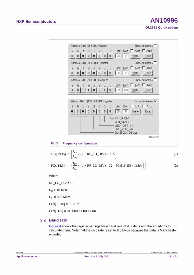
The OL2381 registers allow up to four frequencies to be set. In this application note, only one frequency is set for simplicity. Figure 3 shows the register settings for 868 MHz and the equations to calculate them. Frequencies above 500 MHz require the VCO frequency to be divided by 2 (bit RF_LO_DIV set to logic 0).
Fig 2. General registers flow chart
019aab765
Ports Configuration: PORTCON0, PORTCON1,PORTCON2
TX/RXRXTX
Configuration of the PLL: EXPERT0
Clock Configuration: CLOCKCON
TX Configuration RX Configuration
Baud Rate: TIMING0, TIMING1
Frequency registers: FC0[L, M, H], FC1[L, M, H],FC2[L, M, H]; FC3[L, M, H];LOCON (bit RF_LO_DIV)
OL2381configuration
AN10996 All information provided in this document is subject to legal disclaimers. © NXP B.V. 2011. All rights reserved.
Application note Rev. 1 — 5 July 2011 5 of 21
NXP Semiconductors AN10996OL2381 Quick set-up
(1)
(2)
Where:
RF_LO_DIV = 0.
fref = 16 MHz.
fRF = 868 MHz.
FCx[19:15] = 00110b.
FCx[14:0] = 010000000000000b.
2.2 Baud rate
Figure 4 shows the register settings for a baud rate of 4.8 kbit/s and the equations to calculate them. Note that the chip rate is set to 9.6 kbit/s because the data is Manchester encoded.
Fig 3. Frequency configuration
019aac368
FCx[19:15]fRF
fref------- 1 RF_LO_DIV+ 32.5–=
FCx[14:0]fRF
fref------- 1 RF_LO_DIV+ 32– FCx[19:15] 16384– =
AN10996 All information provided in this document is subject to legal disclaimers. © NXP B.V. 2011. All rights reserved.
Application note Rev. 1 — 5 July 2011 6 of 21

NXP Semiconductors AN10996OL2381 Quick set-up
(3)
(4)
Where:
chip rate = 9600 bit/s.
fref = 16 MHz.
PRESC = 011b.
MAINSC = 00111010101b.
2.3 PLL
The recommended value for PLL bandwidth is ICP 2 as shown in Figure 5.
Fig 4. Baud rate configuration
019aac369
kchipchip_rate 4096 128
fref------------------------------------------------------- 2048 MAINSC+
2PRESC
-----------------------------------------= =
PRESC log28191
2 max 25 min 3000 kchip ------------------------------------------------------------------------------ =
Fig 5. PLL bandwidth configuration
019aac370
AN10996 All information provided in this document is subject to legal disclaimers. © NXP B.V. 2011. All rights reserved.
Application note Rev. 1 — 5 July 2011 7 of 21

NXP Semiconductors AN10996OL2381 Quick set-up
2.4 Ports configuration
Writing to (and reading from) OL2381 registers is always done via the SPI ports. Data can be sent and received either via the SPI or OL2381 ports P10, P11, and P12. In this example, ports are used and register PORTCON2 must be set as shown in Figure 6 (bits SEP_TX_LINES and SEP_RX_OUT set to 11).
The configuration of P14 depends on the RF switch; details are given in the data sheet.
3. TX registers
This section explains how to set the registers used by the transmitter for this application.
The complete transmit flow chart is shown in Figure 7.
Fig 6. Ports configuration
019aac371
AN10996 All information provided in this document is subject to legal disclaimers. © NXP B.V. 2011. All rights reserved.
Application note Rev. 1 — 5 July 2011 8 of 21

NXP Semiconductors AN10996OL2381 Quick set-up
3.1 Power amplifier (PA) configuration
Bits PAM[1:0] in register TXCON set the voltage for the power amplifier voltage regulator. PAM0 (PAM[1:0] set to 00) is the recommended value for power amplifier operation. The Manchester encoded data requires the chip clock to be used as the transmit clock (TXCLKSEL = 1) as shown in Figure 8.
The output power can be trimmed by bits AMH0[4:0] in register ACON0. Setting register ACON0 as shown in Figure 9 should provide an output power of about 10 dBm.
Fig 7. TX register flow chart
PA Configuration:
Register TXCONRegister ACON0 or ACON1
Configuration of the frequency deviation: FDEVConfiguration of the ramp: FRMP
Configuration of the TX flags:- Frequency- Manchester- ASK/FSK
- ACON0/ACON1
TX Configuration
ModulationASK
see Chapter 7
FSK
019aab773Activate Transmit command
Configuration of ACON2Configuration of the ramp: ARMP
Fig 8. PA configuration
019aac314
AN10996 All information provided in this document is subject to legal disclaimers. © NXP B.V. 2011. All rights reserved.
Application note Rev. 1 — 5 July 2011 9 of 21

NXP Semiconductors AN10996OL2381 Quick set-up
3.2 Frequency modulation and deviation
Bit ASK0 (Figure 9) is set to logic 0 for FSK modulation. Register FDEV configures the frequency deviation, which in this example is set to 4.8 kHz as shown in Figure 10.
(5)
(6)
Where:
FDEV = 65536 fdev / fref.
fdev = 4.8 kHz.
fref = 16 MHz.
DOUBLE_SD_RESULT = 0.
RF_LO_DIV = 0.
FDEV_EXP = 001b.
FDEV_MANT = 01010b.
Fig 9. Output power configuration
019aac372
Fig 10. Frequency deviation configuration
019aac315
FDEV_EXP min 7,max 1 DOUBLE_SD_RESULT+1 RF_LO_DIV+
---------------------------------------------------------------------- 2FDEV15.75---------------- log
=
FDEV_MANT min 31 0.5FDEV
2FDEV_EXP
-------------------------+
=
AN10996 All information provided in this document is subject to legal disclaimers. © NXP B.V. 2011. All rights reserved.
Application note Rev. 1 — 5 July 2011 10 of 21

NXP Semiconductors AN10996OL2381 Quick set-up
3.3 TX flags
Transmit mode is entered by sending a transmit command to OL2381 and is activated on the 9th clock edge. Figure 11 shows the transmit command configuration for Manchester encoded data.
3.4 Results
Figure 12 and Figure 13 show spectrum analyzer displays of the transmitted signal and the demodulated signal with the transmitter settings described previously. The OL2381’s registers can either be set manually using the GUI or by loading the configuration file shown in Section 4.8 on page 17.
Frequency channel 0 selected, FSK, Manchester encoding, synchronized mode + activation on 9th clock edge.
Fig 11. Transmit command
019aac159
AN10996 All information provided in this document is subject to legal disclaimers. © NXP B.V. 2011. All rights reserved.
Application note Rev. 1 — 5 July 2011 11 of 21

NXP Semiconductors AN10996OL2381 Quick set-up
Fig 12. Transmitted signal spectrum
Fig 13. Demodulated transmitted signal spectrum
019aac160
019aac161
AN10996 All information provided in this document is subject to legal disclaimers. © NXP B.V. 2011. All rights reserved.
Application note Rev. 1 — 5 July 2011 12 of 21

NXP Semiconductors AN10996OL2381 Quick set-up
4. RX registers
This section describes how to set the registers used by the receiver for this application. The complete receipt flow chart is shown in Figure 14.
4.1 LNA configuration
The LNA is set to high gain mode (default value) as shown in Figure 15.
Fig 14. RX register flow chart
019aab779
ModulationASKFSK
EdgeSlicer
LevelSlicer
RXGAIN (GAINSTEP, HIGAINLIM if needed)
Configuration of the Channel filter bandwidthand modulation choise RXBW
Configuration of the baseband filterRXBBCON
Configuration of the receive mode:RXCON
Configuration of the timing check unit:TIMINGCHK
Configuration of the slicer:SLICERINITL, SLICERINITH
Configuration of the signal monitoring:-
-
Modulation amplitude range: UMODAMPTH;EMODAMPTH; LMODAMPTHRSSI level:UPPERRSSITH, LOWERRSSITH
Activate Receive command
Polling timer NoYes
Configuration ofPOLLWUPTIME
Configuration ofPOLLACTION
Configuration of RXcommand:
Manchester, Gain,Frequency
(according toprevious regsisters)
Configuration of the preamble length: PREACONConfiguration of the preamble data: PREA0 to PREA2
Configuration of RXFOLLOWUP
Configuration of WUPST0 (if needed)
Configuration of SIGMON0, RXDCON0 (if needed)
Configuration of SIGMON1, RXDCON1 (if needed)
Configuration of SIGMON2 (if needed), RXDCON2
see Chapter 7
AN10996 All information provided in this document is subject to legal disclaimers. © NXP B.V. 2011. All rights reserved.
Application note Rev. 1 — 5 July 2011 13 of 21

NXP Semiconductors AN10996OL2381 Quick set-up
4.2 Channel bandwidth configuration
Register RXBW sets the choice of demodulation (ASK/FSK) and channel filter (IF) bandwidth. Bit DEMOD_ASK is set to 0 for FSK modulation. Careful consideration should be given to the choice of bandwidth to optimize receiver performance. It should be close to the bandwidth occupied by the modulated signal. FSK modulation requires the bandwidth to be equal to twice the sum of the modulating frequency and frequency deviation. The frequency tolerance of the crystal oscillators used should also be taken into account.
The frequency deviation is 4.8 kHz and the modulation frequency is 4.8 kbits (4.8 kHz), which is twice the sum of the previous value of 19.2 kHz. The maximum modulation frequency of the 4.8 kbit/s Manchester encoded data is 4.8 kHz. The nearest channel bandwidth value available is 50 kHz, set by CF_BW[6:4] as shown in Figure 16.
4.3 Baseband filter configuration
Register RXBBCON sets the baseband filter cut-off frequency. It should be appropriate to use modulation. The optimum cut-off frequency at 4.8 kHz is 7.095 kHz, set by BASEBAND_FILTER_FC as shown in Figure 17.
Fig 15. LNA configuration
019aac373
Fig 16. Register RXBW
019aac316
AN10996 All information provided in this document is subject to legal disclaimers. © NXP B.V. 2011. All rights reserved.
Application note Rev. 1 — 5 July 2011 14 of 21

NXP Semiconductors AN10996OL2381 Quick set-up
4.4 Manchester decoder setting
The Manchester decoder should be activated by register RXCON, bit RX_MANCHESTER set to logic 1 as shown in Figure 18.
4.5 Slicer configuration
The edge slicer feature is recommended for FSK modulation, SLICERSEL_D[5:4] set to 00 as shown in Figure 19.
Fig 17. Baseband filter configuration
019aac352
Fig 18. Manchester decoder
019aac317
Fig 19. Slicer configuration
019aac374
AN10996 All information provided in this document is subject to legal disclaimers. © NXP B.V. 2011. All rights reserved.
Application note Rev. 1 — 5 July 2011 15 of 21

NXP Semiconductors AN10996OL2381 Quick set-up
4.6 Expected modulation amplitude configuration
The expected peak modulation must be configured to set the receiver to its optimum settings. Register EMODAMPTH (Figure 20) holds the expected peak deviation value which is compared with the received baseband signal. The receiver has to know the deviation frequency of the transmitted signal to ensure correct operation.
(7)
(8)
(9)
Where:
x: real target value.
x = 33256 modulation deviation / 200.
Modulation deviation = 4.8 kHz.
EDGE_MODAMPTH_TH_EXP = 0110b.
EDGE_MODAMPTH_TH_MANT = 1100b.
4.7 RX flags
Receive mode is entered by sending a receive command to OL2381 and is activated on the 9th clock edge. Figure 12 shows the receive command configuration when only data reception is required.
Fig 20. Expected modulation amplitude configuration
019aac375
EMODAMPTH min 32767 EDGE_MODAMP_TH_MANT 2EDGE_MODAMP_TH_EXP =
EDGE_MODAMP_TH_EXP min 15 2max 15 x
7.75--------------------------- log
=
EDGE_MODAMP_TH_MANT min 15x
2EDGE_MODAMP_TH_EXP
-------------------------------------------------------- 0.5+
=
AN10996 All information provided in this document is subject to legal disclaimers. © NXP B.V. 2011. All rights reserved.
Application note Rev. 1 — 5 July 2011 16 of 21

NXP Semiconductors AN10996OL2381 Quick set-up
4.8 Results
Figure 22 shows the transmitted and received data and clock if receiver is set as described in the previous sections. The received data and clock traces are colored blue and green respectively.
The OL2381’s pseudo-random generator is enabled for transmitting data as shown in Figure 22. Bits P10C[2:1] in register PORTCON0 are set to 10 as shown in Figure 23.
The OL2381’s registers can either be set manually using the GUI or by loading the configuration file shown below.
Data reception (no WUPS and preamble), frequency channel 0 selected.
Fig 21. Receive command
019aac162
Fig 22. Received data
019aac164
AN10996 All information provided in this document is subject to legal disclaimers. © NXP B.V. 2011. All rights reserved.
Application note Rev. 1 — 5 July 2011 17 of 21

NXP Semiconductors AN10996OL2381 Quick set-up
The settings used in this application note are available in a configuration file which can be loaded into the OL2381 as shown below:
//Start[LoPSTerRegisterConfiguration]FileFormat = V2.1NoOfConfigs = 1ActiveConfig = 1
[PresetConfig1]DeviceVersion = V0AConfigName = UpdateTime = 04/21/09 16:14:41; x0 x1 x2 x3 x4 x5 x6 x7 x8 x9 xA xB xC xD xE xF; visible in bank 0,101_0x = 00 00 B2 00 00 00 00 00 00 00 00 00 00 00 D5 5901_1x = 24 24 66 00 00 00 00 00 00 00 2A 00 1F 00 00 0001_2x = 20 F0 50 00 00 00 00 04 00 00 6C 00 00 00 -- --01_3x = -- -- -- -- -- -- -- -- -- -- -- -- -- -- -- 01; visible in bank 00_2x = -- -- -- -- -- -- -- -- -- -- -- -- -- -- 00 000_3x = 00 00 00 00 00 04 00 00 00 00 00 00 00 00 00 --; visible in bank 11_2x = -- -- -- -- -- -- -- -- -- -- -- -- -- -- 00 001_3x = 00 02 00 00 00 00 00 00 00 00 00 00 00 00 00 --TxRx = -- -- -- -- -- -- -- -- -- -- -- -- -- -- 8E 8C//Stop
Fig 23. Pseudo-random generator used for transmitting data
019aac163
AN10996 All information provided in this document is subject to legal disclaimers. © NXP B.V. 2011. All rights reserved.
Application note Rev. 1 — 5 July 2011 18 of 21

NXP Semiconductors AN10996OL2381 Quick set-up
5. Abbreviations
Table 1. Abbreviations
Acronym Description
AM Amplitude Modulation
ASK Amplitude-Shift Keying
FM Frequency Modulation
FSK Frequency Shift Keying
GUI Graphic User Interface
LNA Low-Noise Amplifier
PLL Phase-Locked Loop
RF Radio Frequency
RSSI Residual Signal Strength Indicator
RX Receiver
SPI Serial Peripheral Interface
TX Transmitter
VCO Voltage-Controlled Oscillator
WUP Wake UP
WUPS Wake UP Search
XTAL Crystal Oscillator
AN10996 All information provided in this document is subject to legal disclaimers. © NXP B.V. 2011. All rights reserved.
Application note Rev. 1 — 5 July 2011 19 of 21

NXP Semiconductors AN10996OL2381 Quick set-up
6. Legal information
6.1 Definitions
Draft — The document is a draft version only. The content is still under internal review and subject to formal approval, which may result in modifications or additions. NXP Semiconductors does not give any representations or warranties as to the accuracy or completeness of information included herein and shall have no liability for the consequences of use of such information.
6.2 Disclaimers
Limited warranty and liability — Information in this document is believed to be accurate and reliable. However, NXP Semiconductors does not give any representations or warranties, expressed or implied, as to the accuracy or completeness of such information and shall have no liability for the consequences of use of such information.
In no event shall NXP Semiconductors be liable for any indirect, incidental, punitive, special or consequential damages (including - without limitation - lost profits, lost savings, business interruption, costs related to the removal or replacement of any products or rework charges) whether or not such damages are based on tort (including negligence), warranty, breach of contract or any other legal theory.
Notwithstanding any damages that customer might incur for any reason whatsoever, NXP Semiconductors’ aggregate and cumulative liability towards customer for the products described herein shall be limited in accordance with the Terms and conditions of commercial sale of NXP Semiconductors.
Right to make changes — NXP Semiconductors reserves the right to make changes to information published in this document, including without limitation specifications and product descriptions, at any time and without notice. This document supersedes and replaces all information supplied prior to the publication hereof.
Suitability for use — NXP Semiconductors products are not designed, authorized or warranted to be suitable for use in life support, life-critical or safety-critical systems or equipment, nor in applications where failure or malfunction of an NXP Semiconductors product can reasonably be expected to result in personal injury, death or severe property or environmental damage. NXP Semiconductors accepts no liability for inclusion and/or use of NXP Semiconductors products in such equipment or applications and therefore such inclusion and/or use is at the customer’s own risk.
Applications — Applications that are described herein for any of these products are for illustrative purposes only. NXP Semiconductors makes no representation or warranty that such applications will be suitable for the specified use without further testing or modification.
Customers are responsible for the design and operation of their applications and products using NXP Semiconductors products, and NXP Semiconductors accepts no liability for any assistance with applications or customer product
design. It is customer’s sole responsibility to determine whether the NXP Semiconductors product is suitable and fit for the customer’s applications and products planned, as well as for the planned application and use of customer’s third party customer(s). Customers should provide appropriate design and operating safeguards to minimize the risks associated with their applications and products.
NXP Semiconductors does not accept any liability related to any default, damage, costs or problem which is based on any weakness or default in the customer’s applications or products, or the application or use by customer’s third party customer(s). Customer is responsible for doing all necessary testing for the customer’s applications and products using NXP Semiconductors products in order to avoid a default of the applications and the products or of the application or use by customer’s third party customer(s). NXP does not accept any liability in this respect.
Export control — This document as well as the item(s) described herein may be subject to export control regulations. Export might require a prior authorization from national authorities.
Evaluation products — This product is provided on an “as is” and “with all faults” basis for evaluation purposes only. NXP Semiconductors, its affiliates and their suppliers expressly disclaim all warranties, whether express, implied or statutory, including but not limited to the implied warranties of non-infringement, merchantability and fitness for a particular purpose. The entire risk as to the quality, or arising out of the use or performance, of this product remains with customer.
In no event shall NXP Semiconductors, its affiliates or their suppliers be liable to customer for any special, indirect, consequential, punitive or incidental damages (including without limitation damages for loss of business, business interruption, loss of use, loss of data or information, and the like) arising out the use of or inability to use the product, whether or not based on tort (including negligence), strict liability, breach of contract, breach of warranty or any other theory, even if advised of the possibility of such damages.
Notwithstanding any damages that customer might incur for any reason whatsoever (including without limitation, all damages referenced above and all direct or general damages), the entire liability of NXP Semiconductors, its affiliates and their suppliers and customer’s exclusive remedy for all of the foregoing shall be limited to actual damages incurred by customer based on reasonable reliance up to the greater of the amount actually paid by customer for the product or five dollars (US$5.00). The foregoing limitations, exclusions and disclaimers shall apply to the maximum extent permitted by applicable law, even if any remedy fails of its essential purpose.
6.3 TrademarksNotice: All referenced brands, product names, service names and trademarks are the property of their respective owners.
AN10996 All information provided in this document is subject to legal disclaimers. © NXP B.V. 2011. All rights reserved.
Application note Rev. 1 — 5 July 2011 20 of 21

NXP Semiconductors AN10996OL2381 Quick set-up
7. Contents
1 Introduction . . . . . . . . . . . . . . . . . . . . . . . . . . . . 3
2 General registers . . . . . . . . . . . . . . . . . . . . . . . . 52.1 Frequency. . . . . . . . . . . . . . . . . . . . . . . . . . . . . 52.2 Baud rate . . . . . . . . . . . . . . . . . . . . . . . . . . . . . 62.3 PLL . . . . . . . . . . . . . . . . . . . . . . . . . . . . . . . . . . 72.4 Ports configuration . . . . . . . . . . . . . . . . . . . . . . 8
3 TX registers . . . . . . . . . . . . . . . . . . . . . . . . . . . . 83.1 Power amplifier (PA) configuration . . . . . . . . . . 93.2 Frequency modulation and deviation . . . . . . . 103.3 TX flags . . . . . . . . . . . . . . . . . . . . . . . . . . . . . 113.4 Results . . . . . . . . . . . . . . . . . . . . . . . . . . . . . . 11
4 RX registers . . . . . . . . . . . . . . . . . . . . . . . . . . . 134.1 LNA configuration . . . . . . . . . . . . . . . . . . . . . . 134.2 Channel bandwidth configuration . . . . . . . . . . 144.3 Baseband filter configuration . . . . . . . . . . . . . 144.4 Manchester decoder setting . . . . . . . . . . . . . . 154.5 Slicer configuration . . . . . . . . . . . . . . . . . . . . . 154.6 Expected modulation amplitude
configuration . . . . . . . . . . . . . . . . . . . . . . . . . . 164.7 RX flags . . . . . . . . . . . . . . . . . . . . . . . . . . . . . 164.8 Results . . . . . . . . . . . . . . . . . . . . . . . . . . . . . . 17
5 Abbreviations. . . . . . . . . . . . . . . . . . . . . . . . . . 19
6 Legal information. . . . . . . . . . . . . . . . . . . . . . . 206.1 Definitions. . . . . . . . . . . . . . . . . . . . . . . . . . . . 206.2 Disclaimers . . . . . . . . . . . . . . . . . . . . . . . . . . . 206.3 Trademarks. . . . . . . . . . . . . . . . . . . . . . . . . . . 20
7 Contents . . . . . . . . . . . . . . . . . . . . . . . . . . . . . . 21
© NXP B.V. 2011. All rights reserved.
For more information, please visit: http://www.nxp.comFor sales office addresses, please send an email to: [email protected]
Date of release: 5 July 2011
Document identifier: AN10996
Please be aware that important notices concerning this document and the product(s)described herein, have been included in section ‘Legal information’.