an10436 tda8932b/33(b) class-d audio amplifier · document information an10436 tda8932b/33(b)...
TRANSCRIPT

AN10436TDA8932B/33(B) Class-D audio amplifierRev. 01 — 12 December 2007 Application note
Document informationInfo ContentKeywords Class-D amplifier, High efficiency, Switch mode amplifier, Flat TV.
Abstract This application note describes a stereo Switched Mode Amplifier (SMA) for audio, based on either the TDA8932B or TDA8933(B) Class-D audio amplifier device of NXP Semiconductors, which has been designed for Flat TV applications.The TDA8932B device is the high-power version that delivers an output power of 2 × 10 WRMS to 2 × 25 WRMS in a Single Ended (SE) configuration or 10 WRMS to 50 WRMS in a Bridge Tied Load (BTL) configuration.The TDA8933(B) device is the low-power version that delivers an output power of 2 × 5 WRMS to 2 × 15 WRMS in a SE configuration or 10 WRMS to 30 WRMS in a BTL configuration.This high efficiency SMA device has been designed to operate without a heat sink and has the flexibility to operate from either an asymmetrical supply or a symmetrical supply with a wide range (10 V to 36 V or ±5 V to ±18 V).The TDA8932B/33(B) device utilizes two advanced features, the Thermal Foldback (TF) and the cycle-by-cycle current limiting to avoid audio holes (interruptions) during normal operation.In addition, the TDA8932B/33(B) utilizes integrated Half Supply Voltage (HVP) buffers to simplify the design for an asymmetrical supply in the SE configuration. Control logic is integrated for a pop free transition between on/off. A SLEEP mode is incorporated to comply with the power saving regulations.An application designed around the TDA8932B/33(B) device is very robust because of the internal protection features, such as a number of voltage protections, OverCurrent Protection (OCP) and OverTemperature Protection (OTP).

NXP Semiconductors AN10436TDA8932B/33(B) Class-D audio amplifier
Revision historyRev Date Description
01.00 20071212 First release
AN10436_1 © NXP B.V. 2007. All rights reserved.
Application note Rev. 01 — 12 December 2007 2 of 55
Contact informationFor additional information, please visit: http://www.nxp.com
For sales office addresses, please send an email to: [email protected]
NXP Semiconductors AN10436TDA8932B/33(B) Class-D audio amplifier
1. Introduction
This application note describes a reference design of a Switched Mode Amplifier (SMA) for audio, based on the TDA8932B or TDA8933(B) device of NXP Semiconductors operating from an asymmetrical supply.
The TDA8932B device and the TDA8933(B) device are pin-to-pin compatible and can be used in either a stereo SE configuration or a mono BTL configuration. The TDA8932B is the high-power version and the TDA8933(B) is the low-power version. Together they cover a wide power range per channel of 5 WRMS to 50 WRMS. The two versions are available in the SO32 package (TDA8932BT, TDA8933T) and the HTSSOP32 package (TDA8932BTW, TDA8933BTW). The TDA8932B/33(B) Class-D amplifier is intended for:
• Flat TV application• Flat panel monitors• Multimedia systems, docking stations• Wireless speakers• Microsystems
Distinctive features
• High efficiency Class-D audio amplifier due to a low RDSon in SE configuration.• Operates from a wide voltage range 10 V to 36 V (asymmetrical) or ±5 V to ±18 V
(symmetrical).• Maximum power capability:
– TDA8932B is 2 × 30 WRMS short time output power in 4 Ω SE without heat sink.– TDA8933(B) is 2 × 20 WRMS short time output power in 8 Ω SE without heat sink.
• Cycle-by-cycle current limiting to avoid interruption during normal operation.• Unique Thermal Foldback (TF) to avoid interruption during normal operation.• Integrated Half Supply Voltage (HVP) buffers for reference and SE output capacitance
(asymmetrical supply).• Internal logic for pop free power supply on/off cycling.• Low standby current in SLEEP mode for power saving regulations.
Protection features
• Window Protection (WP)• UnderVoltage Protection (UVP)• OverVoltage Protection (OVP)• UnBalance Protection (UBP)• OverCurrent Protection (OCP)• OverTemperature Protection (OTP)• ESD protection
These features enable an engineer to design a high performance, reliable and cost effective SMA with only a small number of external components.
AN10436_1 © NXP B.V. 2007. All rights reserved.
Application note Rev. 01 — 12 December 2007 3 of 55

NXP Semiconductors AN10436TDA8932B/33(B) Class-D audio amplifier
1.1 Block diagram
1.2 Fixed frequency pulse width modulated Class-D conceptThe TDA8932B/33(B) device is a closed loop fixed frequency pulse width modulated Class-D amplifier with two differential analog inputs, each driving an independent power stage (see Figure 2). The power stage consists out of a low side and a high side N-channel MOSFET.
Fig 1. Block diagram
001aaf597
2
10 31 828
29
27
3
12
TDA8932B
OSCILLATOR
26
BOOT1
VDDP1
OUT1
VSSP1
PWMMODULATOR
DRIVERHIGH
DRIVERLOW
CTRL
MANAGER
CTRLPWM
MODULATOR
PROTECTIONS:OVP, OCP, OTP,
UVP, TF, WPSTABILIZER 11 V
STABILIZER 11 V
REGULATOR 5 V
MODE
VDDA
15
14
IN1P
OSCREF OSCIO VDDA
VSSD
IN1N
INREF
IN2P
IN2N
6POWERUP
4DIAG
7CGND
21
20
22
23
BOOT2
VDDP2
OUT2
25 STAB1
24 STAB2
18
11
DREF
HVPREF
30 HVP1
19 HVP2
VSSP2
DRIVERHIGH
DRIVERLOW
VDDA
VSSP1
VSSP2
VSSD
VDDA
VSSA
HALF SUPPLY VOLTAGE
5ENGAGE
13
9
TEST
VSSA
1, 16, 17, 32
VSSD(HW)
AN10436_1 © NXP B.V. 2007. All rights reserved.
Application note Rev. 01 — 12 December 2007 4 of 55

NXP Semiconductors AN10436TDA8932B/33(B) Class-D audio amplifier
The TDA8932B/33(B) can be configured for use in either SE or BTL. The major benefits of an SE configuration compared to a BTL configuration are cost and efficiency. This is because:
• Only one pair of power switches is required for each channel.• Only one LP filter (inductor and film capacitor) is required for each channel.• Only two power stages for stereo in one package, therefore no heat sink required.
An internal feedback network has a fixed closed loop gain of 30 dB in the SE configuration (36 dB in the BTL configuration).
The Pulse Width Modulation (PWM) output signal has a oscillator frequency that is fixed by either:
• An internal oscillator when configured as master.• An external oscillator when configured as slave.
The pulse width will be modulated according to the input signal.
Section 3 describes the complete application design of the TDA8932B/33(B) and includes the dimensioning of the LP output filter.
1.3 Typical application circuits (simplified)
1.3.1 Asymmetrical supply stereo SE configurationThe simplified application circuit of the TDA8932B/33(B) device when operated from an asymmetrical supply (single supply) can be seen in Figure 3. The TDA8932B/33(B) incorporates three integrated half supply voltage buffers to simplify the design for an asymmetrical supply in SE configuration. One buffer is for the reference decoupling capacitor (CHVPREF) on HVPREF (pin 11) and two other buffers are for the two AC-couple capacitors (CSE) in series with the speaker.
Fig 2. TDA8932B/33(B) in SE configuration
IN1P 2
IN1N
3
TDA8932B/33(B)
IN2N 14
IN2P
15
27
22
PWM
OUT1
PWM
OUT2
CSE
LPFILTER
010aaa000
CSE
LPFILTER
AN10436_1 © NXP B.V. 2007. All rights reserved.
Application note Rev. 01 — 12 December 2007 5 of 55
NXP Semiconductors AN10436TDA8932B/33(B) Class-D audio amplifier
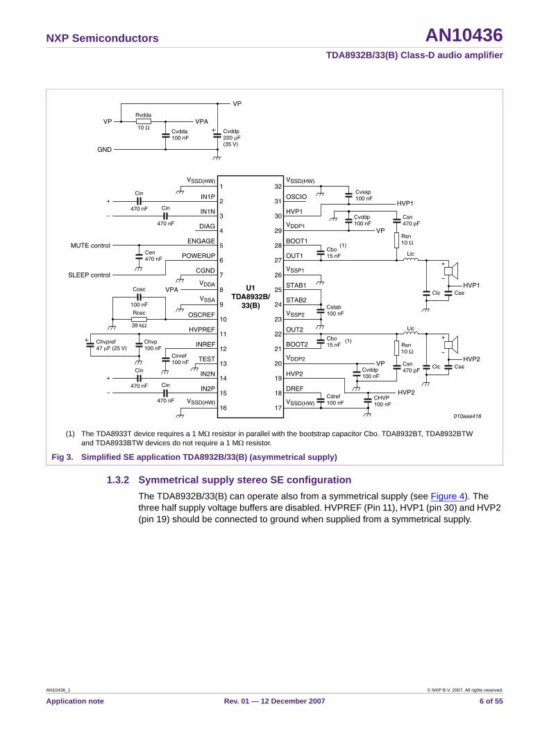
1.3.2 Symmetrical supply stereo SE configurationThe TDA8932B/33(B) can operate also from a symmetrical supply (see Figure 4). The three half supply voltage buffers are disabled. HVPREF (Pin 11), HVP1 (pin 30) and HVP2 (pin 19) should be connected to ground when supplied from a symmetrical supply.
(1) The TDA8933T device requires a 1 MΩ resistor in parallel with the bootstrap capacitor Cbo. TDA8932BT, TDA8932BTW and TDA8933BTW devices do not require a 1 MΩ resistor.
Fig 3. Simplified SE application TDA8932B/33(B) (asymmetrical supply)
U1TDA8932B/
33(B)
VSSD(HW)
470 nF
Cin
Cen470 nF
VSSD(HW)
IN1P
Cinref100 nF
Chvp100 nF
Chvpref47 μF (25 V)
Cvddp220 μF(35 V)
470 nF
Cin
470 nF
Cin
470 nF
Cin
100 nF
Cosc
39 kΩ
Rosc
10 Ω
Rvdda
MUTE control
VPA
SLEEP control
Cvdda100 nF
VP VPA
VP
GND
OSCIO
IN1N HVP1
DIAG VDDP1
ENGAGE BOOT1
POWERUP OUT1
CGND VSSP1
VDDA STAB1
VSSA STAB2
OSCREF VSSP2
HVPREF OUT2
INREF BOOT2
TEST VDDP2
IN2N HVP2
IN2P DREF
VSSD(HW) VSSD(HW)
010aaa418
1
2
3
4
5
6
7
8
9
10
11
12
13
14
15
16
18
17
20
19
22
21
24
23
26
25
32
31
30
29
28
27
+
−
+
− Csn470 pF
Csn470 pF
Rsn10 Ω
Rsn10 Ω
Llc
Llc
Cdref100 nF
HVP1
VP
Cstab100 nF
Clc
Cvddp100 nF
Cvddp100 nF
VP
Cbo15 nF
Cvssp100 nF
Cbo15 nF
CseHVP1
Clc CseHVP2
CHVP100 nF
HVP2
(1)
(1)
AN10436_1 © NXP B.V. 2007. All rights reserved.
Application note Rev. 01 — 12 December 2007 6 of 55

NXP Semiconductors AN10436TDA8932B/33(B) Class-D audio amplifier
A symmetrical supply has some benefits compared to an asymmetrical supply. First, the power bandwidth is not limited by the size of the SE capacitor. Therefore, for a full bandwidth (20 Hz to 20 kHz) amplifier, a symmetrical supply should be considered to avoid a large value SE capacitor. Secondly, when the supply is either unregulated and/or weak (e.g., a 50 Hz / 60 Hz transformer), the output signal will not suffer from asymmetrical clipping (see Section 4.4).
1.3.3 Asymmetrical supply mono BTL configurationThe TDA8932B/33(B) can operate in BTL configuration when a high output power is required at a low supply voltage (e.g., for driving a subwoofer in a 2.1 system). See Figure 5.
(1) The TDA8933T device requires a 1 MΩ resistor in parallel with the bootstrap capacitor Cbo. TDA8932BT, TDA8932BTW and TDA8933BTW devices do not require a 1 MΩ resistor.
Fig 4. Simplified SE application TDA8932B/33(B) (symmetrical supply)
U1TDA8932B/
33(B)
VSSD(HW)
470 nF
Cin
Cen470 nF
Csn470 pF
Csn470 pF
Rsn10 Ω
Rsn10 Ω
Llc
Llc
VSSD(HW)
IN1P
Cdref100 nF
Cinref100 nF
Cvddp220 μF(25 V)
470 nF
Cin
470 nF
Cin
470 nF
Cin
100 nF
Cosc
39 kΩ
Rosc
10 Ω
Rvdda
MUTE control
VDDA
VSSA
VSS
VSSVSSA
VSSA
VSSA
VSSA
SLEEP control
Cvdda100 nF
VDD VDDA
10 Ω
RvssaVSS VSSA
VDD
VSS
Cvssa100 nF
Cvssp220 μF(25 V)
GND
OSCIO
IN1N HVP1
DIAG VDDP1
ENGAGE BOOT1
VDD
POWERUP OUT1
CGND VSSP1
VDDA STAB1
VSSA STAB2
OSCREF VSSP2
HVPREF OUT2
INREF
Cstab100 nF
Clc
ClcBOOT2
TEST VDDP2
IN2N HVP2
IN2P DREF
VSSD(HW) VSSD(HW)
010aaa419
1
2
3
4
5
6
7
8
9
10
11
12
13
14
15
16
18
17
20
19
22
21
24
23
26
25
32
31
30
29
28
27
VSSA
Cvddp100 nF
Cvddp100 nF
VSS
VDD
Cbo15 nF
+
−
+
−
Cvssp100 nF
Cbo15 nF
Cvssp100 nF
VSS
(1)
(1)
VSSA
AN10436_1 © NXP B.V. 2007. All rights reserved.
Application note Rev. 01 — 12 December 2007 7 of 55

NXP Semiconductors AN10436TDA8932B/33(B) Class-D audio amplifier
1.3.4 Symmetrical supply mono BTL configurationThe TDA8932B/33(B) can operate in BTL configuration when high output powers are required at a low supply voltage (e.g., for driving a subwoofer in a 2.1 system). See Figure 6.
(1) The TDA8933T device requires a 1 MΩ resistor in parallel with the bootstrap capacitor Cbo. TDA8932BT, TDA8932BTW and TDA8933BTW devices do not require a 1 MΩ resistor.
Fig 5. Simplified BTL application TDA8932B/33(B) (asymmetrical supply)
U1TDA8932B/
33(B)
VSSD(HW)
470 nF
Cin
Cen470 nF
Csn470 pF
Rsn10 Ω
Llc
Llc
VSSD(HW)
IN1P
Cinref100 nF
Chvp100 nF
470 nF
Cin
100 nF
Cosc
39 kΩ
Rosc
MUTEcontrol
VPA
SLEEPcontrol
OSCIO
IN1N HVP1
DIAG VDDP1
ENGAGE BOOT1
POWERUP OUT1
CGND VSSP1
VDDA STAB1
VSSA STAB2
OSCREF VSSP2
HVPREF OUT2
INREF
Cstab100 nF
Clc
Clc
BOOT2
TEST VDDP2
IN2N HVP2
IN2P DREF
VSSD(HW) VSSD(HW)
010aaa420
1
2
3
4
5
6
7
8
9
10
11
12
13
14
15
16
18
17
20
19
22
21
24
23
26
25
32
31
30
29
28
27
Cvddp220 μF(35 V)
10 Ω
Rvdda
Cvdda100 nF
VP VPA
VP
GND
+
−
HVPREF
Csn470 pF
Rsn10 Ω
Cdref100 nF
Cvddp100 nF
VP
Cbo15 nF
Chvp100 nF
Rhvp
470 ΩHVPREF
Csn470 pF
Rsn10 Ω
HVPREF
VP
Cvddp100 nF
Cbo15 nF
Chvp100 nF Rhvp
470 Ω
(1)
(1)
AN10436_1 © NXP B.V. 2007. All rights reserved.
Application note Rev. 01 — 12 December 2007 8 of 55

NXP Semiconductors AN10436TDA8932B/33(B) Class-D audio amplifier
2. Functional IC description
This chapter briefly describes the main functionality of the TDA8932B/33(B) device and the different modes. It also describes the different features and the protections implemented in the TDA8932B/33(B). Table 3 in Section 2.8 in gives a description of each pin.
2.1 Control inputsThe TDA8932B/33(B) is controlled by two inputs, POWERUP (pin 6) and ENGAGE (pin 5). The POWERUP is a two-level high impedance input. The ENGAGE input has an internal pull-up current source and an internal pull-down resistor of 100 kΩ (typical). The internal pull-up current source is enabled after the power stages are
(1) The TDA8933T device requires a 1 MΩ resistor in parallel with the bootstrap capacitor Cbo. TDA8932BT, TDA8932BTW and TDA8933BTW devices do not require a 1 MΩ resistor.
Fig 6. Simplified BTL application TDA8932B/33(B) (symmetrical supply)
U1TDA8932B/
33(B)
VSSD(HW)
Cen470 nF
Llc
Llc
VSSD(HW)
IN1P
Cinref100 nF
100 nF
Cosc
39 kΩ
Rosc
MUTEcontrol
VDDA
VSSA
VSSA
VSSA
VSSA
SLEEPcontrol
OSCIO
IN1N HVP1
DIAG VDDP1
ENGAGE BOOT1
POWERUP OUT1
CGND VSSP1
VDDA STAB1
VSSA STAB2
OSCREF VSSP2
HVPREF OUT2
INREF
Cstab100 nF
Clc
Clc
BOOT2
TEST VDDP2
IN2N HVP2
IN2P DREF
VSSD(HW) VSSD(HW)
010aaa421
1
2
3
4
5
6
7
8
9
10
11
12
13
14
15
16
18
17
20
19
22
21
24
23
26
25
32
31
30
29
28
27
Cvddp220 μF(25 V)
10 Ω
Rvdda
Cvdda100 nF
VDD VDDA
10 Ω
RvssaVSS VSSA
VDD
VSS
Cvssa100 nF
Cvssp220 μF(25 V)
GND
1 μF
Cin
1 μF
Cin
VSS
Csn470 pF
Rsn10 Ω
VSSVSSA
VDD
Cvddp100 nF
Cbo15 nF
Cvssp100 nF
Csn470 pF
Rsn10 Ω
Cdref100 nF
VSSA
Cvddp100 nF
VDD
Cbo15 nF
Cvssp100 nF
VSS
VSS
+
−
(1)
(1)
VSSA
AN10436_1 © NXP B.V. 2007. All rights reserved.
Application note Rev. 01 — 12 December 2007 9 of 55
NXP Semiconductors AN10436TDA8932B/33(B) Class-D audio amplifier
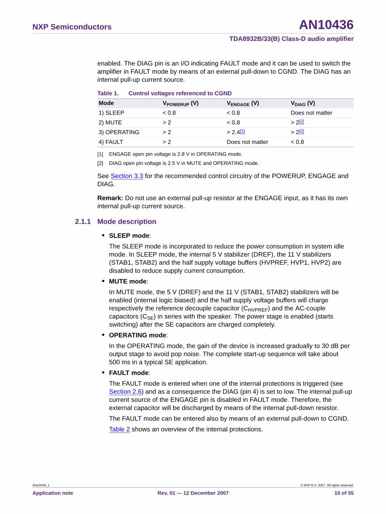
enabled. The DIAG pin is an I/O indicating FAULT mode and it can be used to switch the amplifier in FAULT mode by means of an external pull-down to CGND. The DIAG has an internal pull-up current source.
[1] ENGAGE open pin voltage is 2.8 V in OPERATING mode.
[2] DIAG open pin voltage is 2.5 V in MUTE and OPERATING mode.
See Section 3.3 for the recommended control circuitry of the POWERUP, ENGAGE and DIAG.
Remark: Do not use an external pull-up resistor at the ENGAGE input, as it has its own internal pull-up current source.
2.1.1 Mode description
• SLEEP mode:The SLEEP mode is incorporated to reduce the power consumption in system idle mode. In SLEEP mode, the internal 5 V stabilizer (DREF), the 11 V stabilizers (STAB1, STAB2) and the half supply voltage buffers (HVPREF, HVP1, HVP2) are disabled to reduce supply current consumption.
• MUTE mode:In MUTE mode, the 5 V (DREF) and the 11 V (STAB1, STAB2) stabilizers will be enabled (internal logic biased) and the half supply voltage buffers will charge respectively the reference decouple capacitor (CHVPREF) and the AC-couple capacitors (CSE) in series with the speaker. The power stage is enabled (starts switching) after the SE capacitors are charged completely.
• OPERATING mode:In the OPERATING mode, the gain of the device is increased gradually to 30 dB per output stage to avoid pop noise. The complete start-up sequence will take about 500 ms in a typical SE application.
• FAULT mode:The FAULT mode is entered when one of the internal protections is triggered (see Section 2.6) and as a consequence the DIAG (pin 4) is set to low. The internal pull-up current source of the ENGAGE pin is disabled in FAULT mode. Therefore, the external capacitor will be discharged by means of the internal pull-down resistor.The FAULT mode can be entered also by means of an external pull-down to CGND.Table 2 shows an overview of the internal protections.
Table 1. Control voltages referenced to CGNDMode VPOWERUP (V) VENGAGE (V) VDIAG (V)1) SLEEP < 0.8 < 0.8 Does not matter
2) MUTE > 2 < 0.8 > 2[2]
3) OPERATING > 2 > 2.4[1] > 2[2]
4) FAULT > 2 Does not matter < 0.8
AN10436_1 © NXP B.V. 2007. All rights reserved.
Application note Rev. 01 — 12 December 2007 10 of 55
NXP Semiconductors AN10436TDA8932B/33(B) Class-D audio amplifier
2.2 Half Supply Voltage (HVP) chargersThe internal HVPREF, HVP1 and HVP2 buffers will quickly charge the reference capacitor (CHVPREF) and the SE capacitors (CSE) before the power stage is enabled. The typical charge current of the HVP1 (pin 30) and the HVP2 (pin 19) buffers is 80 mA (dependent on the junction temperature). The charge time of the SE capacitor can be estimated as follows:
(1)
Where:
CSE = single ended capacitor (F)VDDA = analog supply voltage (V)VSSA = negative analog supply voltage (V)I = typical charge current (A)
Example:
Charging an SE capacitor of 1000 μF at a supply voltage of 22 V takes about 138 ms.
Remark: The half supply voltage buffers are short circuit protected.
2.3 Pop free power supply on/off cycling
2.3.1 Supply turn-onInternal logic will delay the operation (regardless of the control voltages) until the HVPREF, HVP1 and HVP2 buffers are settled at ½(VDDA − VSSA) to avoid pop noise. For an optimum pop performance, a capacitor of 470 nF should be attached to the ENGAGE (pin 5). This will make sure the gain and therefore the offset will be increased gradually to avoid pop sound (see Figure 21).
2.3.2 Supply turn-offEither the UnBalance Protection (UBP) or the UnderVoltage Protection (UVP) will avoid pop noise when the power supply is turned off. The power stage is disabled when either VDDA drops more than 20 % (see Section 2.6.6 for more detail) or the UVP threshold level (9.5 V typical) is reached.
Remark: During power supply on/off cycling, an unwanted input signal from the audio source can still cause a pop noise. To prevent this the ENGAGE pin should be pulled down to CGND to mute any unwanted signal.
2.4 Oscillator frequencyAn external resistor connected between the OSCREF (pin 10) and VSSA sets the oscillator frequency of the PWM output. The oscillator frequency can be estimated with this equation:
(2)
tCSE 0.5 VDDA VSSA–( )⋅ ⋅
I--------------------------------------------------------------=
fosc12.45 109⋅
Rosc--------------------------=
AN10436_1 © NXP B.V. 2007. All rights reserved.
Application note Rev. 01 — 12 December 2007 11 of 55

NXP Semiconductors AN10436TDA8932B/33(B) Class-D audio amplifier
Where:
Rosc = resistor to set the oscillator frequency.
The oscillator frequency can be set between 250 kHz and 500 kHz.
Example:
The use of a 39 kΩ resistor will result in a oscillator frequency of about 320 kHz.
Remark: A decouple capacitor of 100 nF should be connected across Rosc for noise reduction.
Remark: Synchronization is recommended when two or more TDA8932B/33(B) devices are used in the same application (see Section 2.5).
2.5 Device synchronizationSynchronization is recommended to avoid possible audible beat tones from the speakers when two or more TDA8932B/33(B) devices are used in the same application. Synchronization can be achieved by connecting all OSCIOs (pin 31) together and configuring one of the devices as master, while the other TDA8932B/33(B) device is configured as slave (see Figure 7).
A device is configured as master when a resistor is connected between OSCREF (pin 10) and VSSA to set the oscillator frequency. The OSCIO (pin 31) of the master is then configured as an oscillator output for synchronization. The OSCREF (pin 10) of the slave devices should be shortened to VSSA to configure the OSCIO as an input.
Remark: In a 2.1 system, the SE device for the L/R channel should be configured as master.
Remark: The maximum number of slaves driven by one master is 12.
Fig 7. Device synchronization in a 2.1 system
VSSA OSCREF OSCIO VSSA OSCREF OSCIO
MASTERL/R CHANNEL
SLAVESUBWOOFER CHANNEL
TDA8932B/33(B)
31 3199 10
Rosc39 kΩ
Cosc100 nF
10
010aaa001
TDA8932B/33(B)
VSSAVSSA
AN10436_1 © NXP B.V. 2007. All rights reserved.
Application note Rev. 01 — 12 December 2007 12 of 55

NXP Semiconductors AN10436TDA8932B/33(B) Class-D audio amplifier
2.6 Limiting and protection featuresThe TDA8932B/33(B) device utilizes two advanced limiting features, the thermal foldback and the cycle-by-cycle current limiting, to avoid audio holes (interruptions) during normal operation.
In addition to these limiting features the device has several protection features that make the TDA8932B/33(B) very robust during a fault condition. The following protections are incorporated:
• Window Protection (WP)• UnderVoltage Protections (UVP)• OverVoltage Protection (OVP)• UnBalance Protection (UBP)• OverCurrent Protection (OCP)• OverTemperature Protection (OTP)
When one of the above protections is triggered, the device will enter the FAULT mode and the power stage is disabled immediately (floating). Furthermore, an internal timer of about 100 ms is started and the DIAG (pin 4), referenced to CGND, is set low for the first 50 ms of the timer to indicate this protection status (FAULT mode). In addition the internal pull-up current of the ENGAGE pin is disabled in the FAULT mode, so the external capacitor will be discharged by means of the internal pull-down resistor (100 kΩ). After about 100 ms the device will restart (self-recovering), but only when the fault condition has been resolved.
A microcontroller can use the diagnostic signal (DIAG) to, e.g., shut down either the amplifier or the power supply.
Table 2. Overview of all the limiting and protection features inside the TDA8932B/33(B)Feature Trigger level DIAG
outputRemark
Min Typ MaxTF - 140 °C - 150 °C high Unique thermal limiting to avoid audio holes
when the junction temperature exceeds 140 °C during normal operation. (See Section 2.6.1)
Cycle-by-cycle current limiting
TDA8932B 4.0 A 5.0 A - high Unique current limiting to avoid audio holes when the current exceeds the trigger level during normal operation. (See Section 2.6.2)
TDA8933(B) 2.0 A 2.3 A -
WP[1] low level 7.6[1] - - low[2] Power stage stays floating and entering FAULT mode. (See Section 2.6.3)high level 14.4[1] - -
UVP (VDDA − VSSA)
- 8.0 V 9.5 V 10 V low[2] Power stage becomes floating entering FAULT mode. (See Section 2.6.4)
OVP (VDDA − VSSA)
- 36 V 38.5 V 40 V low[2] Power stage becomes floating entering FAULT mode. (See Section 2.6.5)
UBP[3] low level - 17.6 V[3] - low[2] Power stage becomes floating entering FAULT mode. (See Section 2.6.6)high level - 29.3 V[3] -
AN10436_1 © NXP B.V. 2007. All rights reserved.
Application note Rev. 01 — 12 December 2007 13 of 55

NXP Semiconductors AN10436TDA8932B/33(B) Class-D audio amplifier
[1] WP threshold level at VP = 22 V. See Equation 3 and Equation 4 for the threshold level versus the supply voltage.
[2] DIAG is active low for at least 50 ms.
[3] UBP threshold level at VP = 22 V. See Equation 5 and Equation 6 for the threshold level versus the supply voltage.
2.6.1 Thermal Foldback (TF)When the junction of the TDA8932B/33(B) exceeds 140 °C, the TF will gradually reduce the gain, limiting the power dissipation. This means that the device will not switch off, but will continue to operate at a slightly lower gain, causing no audio holes (interruptions). The maximum junction temperature will not go beyond the absolute maximum temperature. Therefore, a heat sink is not required and the thermal design becomes less critical and less temperature head room requires to be taken into account since audio holes will not occur and the device will always stay within the Safe Operating Area (SOA).
2.6.2 Cycle-by-cycle current limitingWhen the output current of the device exceeds either 4 A (TDA8932B) or 2 A (TDA8933(B)), the cycle-by-cycle current limitation becomes active. This means the device will not switch off, but continue to operate while limiting the current without causing audio holes (interruptions). The maximum output current will not go beyond the absolute maximum current.
Remark: When the cycle-by-cycle current limiting becomes active, it will cause distortion. See Section 3.2 for information on how to calculate the peak output current, depending on the supply voltage and the speaker impedance.
2.6.3 Window Protection (WP)WP checks the voltage at the PWM outputs (OUT1 pin 27 and OUT2 pin 22) before the power stage is enabled (transition from SLEEP mode to MUTE / OPERATING mode). To avoid large currents flowing, the WP is activated (power stage stays floating) in the event of a short from the PWM output to either VDD or VSS. The DIAG is set to low for at least 50 ms.
The PWM output voltage where the WP becomes active at an asymmetrical supply can be calculated as follows:
Low threshold level:
(3)
OCP Low ohmic short across the load
TDA8932B 4.0 A 5.0 A - low[2] Power stage becomes floating entering FAULT mode. (See Section 2.6.7)TDA8933(B) 2.0 A 2.3 A -
OTP - 155 °C - 160 °C low[2] Power stage becomes floating entering FAULT mode. (See Section 2.6.8)
Table 2. Overview of all the limiting and protection features inside the TDA8932B/33(B) …continued
Feature Trigger level DIAG output
RemarkMin Typ Max
VO wp( )l1132------ VDDA⋅=
AN10436_1 © NXP B.V. 2007. All rights reserved.
Application note Rev. 01 — 12 December 2007 14 of 55

NXP Semiconductors AN10436TDA8932B/33(B) Class-D audio amplifier
High threshold level:
(4)
Where:
VO(wp) = window protection output voltage (low or high). Referenced to VSSA (V).VDDA = analog supply voltage (V).
The TDA8932B/33(B) will recover when the output voltage at OUT1 and OUT2 is within (21/32) VDDA > Vo > (11/32) VDDA.
2.6.4 UnderVoltage Protection (UVP)The TDA8932B/33(B) requires a minimum supply voltage for proper operation. When the supply voltage drops below the UVP threshold level of 9.5 V (typical VDDA − VSSA), the power stage becomes floating and the DIAG is set low for at least 50 ms.
2.6.5 OverVoltage Protection (OVP)An OVP is incorporated because an SE Class-D amplifier is able to increase the supply voltage when it is driven at low audio frequencies. This phenomenon is better known as "supply pumping" (see also Section 4.3). The OVP prevents that supply pumping exceeds the absolute maximum supply voltage rating of the TDA8932B/33(B). This is a protection against self-destruction. The OVP threshold level is an internal fixed level at 38.5 V (typical VDDA − VSSA). Beyond this OVP threshold level the power stage will become floating and the DIAG is set low for at least 50 ms.
Remark: The OVP will neither prevent nor limit an overvoltage caused by the power supply.
2.6.6 UnBalance Protection (UBP)The UBP senses the supply voltage unbalance between the analog supply voltages VDDA and VSSA with respect to the HVPREF voltage at pin 11. The UBP is triggered when the unbalance exceeds a certain level to avoid improper biasing resulting in e.g. pop. The DIAG is set low and remains low for at least 50 ms.
The supply voltage where the UBP becomes active with an asymmetrical supply can be estimated as follows:
Low threshold level:
(5)
High threshold level:
(6)
Where:
VP(ubp) = unbalance protection supply voltage (low and high). VDDA (pin 8) referenced to VSSA (V).
VO wp( )h2132------ VDDA⋅=
VP ubp( )l85--- VHVPREF⋅=
VP ubp( )h83--- VHVPREF⋅=
AN10436_1 © NXP B.V. 2007. All rights reserved.
Application note Rev. 01 — 12 December 2007 15 of 55

NXP Semiconductors AN10436TDA8932B/33(B) Class-D audio amplifier
VHVPREF = half supply voltage reference (pin 11) referenced to VSSA (V)
The TDA8932B/33(B) will recover when the supply voltage is within (8/5) VHVPREF > VP > (8/3) VHVPREF.
The supply voltage at which the UBP becomes active with a symmetrical supply can be estimated as follows:
Low threshold level:
(7)
High threshold level:
(8)
Where:
VDDA(ubp) = unbalance protection analog supply voltage. VDDA (pin 8) referenced to VHVPREF (V), HVPREF is connected to GND.VSSA = negative analog supply voltage (pin 9) referenced to VHVPREF (V)
Example asymmetrical supply (use Equation 5 and Equation 6):
At a supply voltage of 22 V, the voltage on HVPREF is equal to VHVPREF = 11 V. The HVPREF voltage is buffered so the level will change only very slowly. When the supply voltage drops quickly (dV/dt > 4 V/s), the UBP is triggered below 17.6 V. When the supply voltage increases quickly, the UBP is triggered above 29.3 V.
Remark: With either an unregulated or a weak power supply, it might happen that this UBP is triggered, e.g., because of a voltage drop during a transient from no load to full load condition. See Section 4.4 for more detail.
2.6.7 OverCurrent Protection (OCP)The OCP is activated only in a fault condition when the current exceeds 4 A (TDA8932B) or 2 A (TDA8933(B)) because of either a low ohmic short across the load or a low ohmic short from the demodulated output (after the inductor) to either VSS or VDD. The DIAG is set low for 50 ms and the internal timer of 100 ms is started. The timer or the WP will keep the power stage disabled for at least 100 ms. As long as the short remains across the load, this cycle will repeat. The average power dissipation in the TDA8932B/33(B) will be low because the short circuit current will flow only during a very small part of the timer cycle of 100 ms.
When the current exceeds 4 A (TDA8932B) or 2 A (TDA8933(B)) during normal operation, only the cycle-by-cycle current limiting is active without causing any audio holes (interruptions). See also Section 2.6.2.
VDDA ubp( )l35--- VSSA⋅=
VDDA ubp( )h53--- VSSA⋅=
AN10436_1 © NXP B.V. 2007. All rights reserved.
Application note Rev. 01 — 12 December 2007 16 of 55

NXP Semiconductors AN10436TDA8932B/33(B) Class-D audio amplifier
2.6.8 OverTemperature Protection (OTP)The OTP is activated only in a fault condition when the junction temperature exceeds 155 °C (typical) e.g. during a short across the SE capacitor. The DIAG output is set low for at least 50 ms and an internal timer of 100 ms is started. The timer will keep the power stage disabled for at least 100 ms.
When the junction temperature exceeds 140 °C during normal operation, the thermal foldback is active without causing any audio holes (interruptions). See also Section 2.6.1.
2.7 Pinning information
Fig 8. Pin configuration SO32
TDA8932BTTDA8933T
VSSD(HW) VSSD(HW)
IN1P OSCIO
IN1N HVP1
DIAG VDDP1
ENGAGE BOOT1
POWERUP OUT1
CGND VSSP1
VDDA STAB1
VSSA STAB2
OSCREF VSSP2
HVPREF OUT2
INREF BOOT2
TEST VDDP2
IN2N HVP2
IN2P DREF
VSSD(HW) VSSD(HW)
010aaa422
1
2
3
4
5
6
7
8
9
10
11
12
13
14
15
16
18
17
20
19
22
21
24
23
26
25
32
31
30
29
28
27
AN10436_1 © NXP B.V. 2007. All rights reserved.
Application note Rev. 01 — 12 December 2007 17 of 55

NXP Semiconductors AN10436TDA8932B/33(B) Class-D audio amplifier
2.8 Pin description
Fig 9. Pin configuration HTSSOP32
TDA8932BTWTDA8933BTW
VSSD(HW) VSSD(HW)
IN1P OSCIO
IN1N HVP1
DIAG VDDP1
ENGAGE BOOT1
POWERUP OUT1
CGND VSSP1
VDDA STAB1
VSSA STAB2
OSCREF VSSP2
HVPREF OUT2
INREF BOOT2
TEST VDDP2
IN2N HVP2
IN2P DREF
VSSD(HW) VSSD(HW)
010aaa423
1
2
3
4
5
6
7
8
9
10
11
12
13
14
15
16
18
17
20
19
22
21
24
23
26
25
32
31
30
29
28
27
Table 3. Pin descriptionSymbol Pin DescriptionVSSD(HW) 1, 16,
17, 32Negative digital supply voltage and handle wafer connection (heat spreader). With an asymmetrical supply, the VSSD(HW) is connected to the supply ground. With a symmetrical supply, the VSSD(HW) is connected to the negative supply line, VSSA.
IN1P 2 Positive audio input for power stage 1.
IN1N 3 Negative audio input for power stage1.
DIAG 4 Input/output to indicate the FAULT mode. DIAG has an internal pull-up and should left floating when unused.
ENGAGE 5 Input with internal pull-up to switch between MUTE mode and OPERATING mode.
POWERUP 6 Input to switch between SLEEP mode and MUTE mode.
CGND 7 Control ground, reference for POWERUP, ENGAGE and DIAG. This CGND is connected to the supply ground.
VDDA 8 Positive analog supply voltage.
VSSA 9 Negative analog supply voltage.
OSCREF 10 Input to set the frequency for the internal oscillator (master configuration). In slave configuration this pin should be connected to VSSA.
HVPREF 11 Decoupling of the internal half supply voltage reference (asymmetrical supply). With a symmetrical supply, this pin should be connected to the CGND (supply ground).
INREF 12 Decoupling for the input reference voltage.
TEST 13 Test signal input for testing purpose only (leave floating or connect to VSSA).
IN2N 14 Negative audio input for power stage 2.
IN2P 15 Positive audio input for power stage 2.
DREF 18 Decoupling of the internal 5 V regulator.
AN10436_1 © NXP B.V. 2007. All rights reserved.
Application note Rev. 01 — 12 December 2007 18 of 55

NXP Semiconductors AN10436TDA8932B/33(B) Class-D audio amplifier
3. Design 2 x 5 W - 25 W audio amplifier (asymmetrical supply)
This chapter describes a stereo amplifier reference design that is based on the TDA8932BT or the TDA8933(B)T device of NXP Semiconductors (see the schematic Section 3.10). This low-cost stereo Single Ended (SE) amplifier design operates with an asymmetrical supply (10 V to 36 V). The TDA8932BT and the TDA8933(B)T devices are pin-to-pin compatible.
The reference PCB, when mounted with TDA8932BT (high-power version), can deliver a continuous time output power of 2 × 15 WRMS into 4 Ω (VP = 22 V) without a heat sink. The maximum short time output power is equal to 2 × 25 WRMS into 4 Ω (VP = 29 V).
The reference PCB, when mounted with TDA8933(B)T (low-power version), can deliver a continuous time output power of 2 × 15 WRMS into 8 Ω (VP = 31 V) without a heat sink. The maximum short time output power is equal to 2 × 18 WRMS into 8 Ω (VP = 34 V).
This chapter shows the most important equations that can be used as a guideline for any design based on the TDA8932B/33(B).
3.1 Output power estimationThe output power for the SE and the BTL configuration, just before clipping, can be estimated through the use of these equations:
(9)
HVP2 19 Half supply voltage buffer for the SE capacitor of output 2 (asymmetrical supply). With a symmetrical supply, this pin should be connected to the CGND (supply ground).
VDDP2 20 Positive supply voltage for the power stage 2.
BOOT2 21 Bootstrap for the high-side driver, power stage 2.
OUT2 22 PWM output, power stage 2.
VSSP2 23 Negative supply voltage for the power stage 2.
STAB2 24 Decoupling of the internal 11 V regulator for power stage 2.
STAB1 25 Decoupling of the internal 11 V regulator for power stage 1.
VSSP1 26 Negative supply voltage for the power stage 1.
OUT1 27 PWM output, power stage 1.
BOOT1 28 Bootstrap for the high-side driver, channel 1.
VDDP1 29 Positive supply voltage for the power stage 1.
HVP1 30 Half supply voltage buffer for the SE capacitor of output 1 (asymmetrical supply). With a symmetrical supply, this pin should be connected to the CGND (supply ground).
OSCIO 31 Oscillator input in the slave configuration or the oscillator output in the master configuration.
Exposed die pad
Exposed die pad applicable to HTSSOP32 package only. The exposed die pad should be connected to VSSD(HW).
Table 3. Pin descriptionSymbol Pin Description
SE: Po(0.5%)
RLRL RDSon Rs RESR+ + +----------------------------------------------------------⎝ ⎠
⎛ ⎞ 1 tW min( ) fosc⋅–( ) VP⋅ ⋅⎝ ⎠⎛ ⎞
2
8 RL⋅-----------------------------------------------------------------------------------------------------------------------------------=
AN10436_1 © NXP B.V. 2007. All rights reserved.
Application note Rev. 01 — 12 December 2007 19 of 55
NXP Semiconductors AN10436TDA8932B/33(B) Class-D audio amplifier
(10)
Where:
VP = supply voltage (V) (VDDP − VSSP)RL = load impedance (Ω)RDSon = on-resistance power switch (Ω)Rs = series resistance output inductor (Ω)RESR = equivalent series resistance of SE capacitance (Ω)tW(min) = minimum pulse width (s) (80 ns typical)fosc = oscillator frequency (Hz) (320 kHz typical R7 = 39 kΩ)
Remark: Equation 9 and Equation 10 are valid only when:
Peak output current ≤ 4 A for TDA8932B (see Section 3.2).Peak output current ≤ 2 A for TDA8933(B).
The output power at 10 % THD can be estimated as follows:
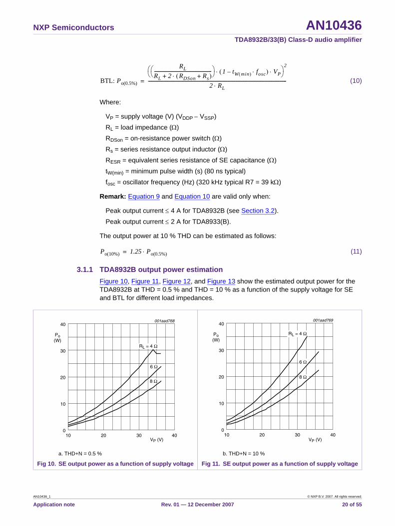
(11)
3.1.1 TDA8932B output power estimationFigure 10, Figure 11, Figure 12, and Figure 13 show the estimated output power for the TDA8932B at THD = 0.5 % and THD = 10 % as a function of the supply voltage for SE and BTL for different load impedances.
BTL: Po(0.5%)
RLRL 2 RDSon Rs+( )⋅+----------------------------------------------------⎝ ⎠
⎛ ⎞ 1 tW min( ) fosc⋅–( ) VP⋅ ⋅⎝ ⎠⎛ ⎞
2
2 RL⋅-----------------------------------------------------------------------------------------------------------------------------=
Po(10%) 1.25 Po(0.5%)⋅=
a. THD+N = 0.5 % b. THD+N = 10 %
Fig 10. SE output power as a function of supply voltage Fig 11. SE output power as a function of supply voltage
VP (V)10 403020
20
10
30
40
Po(W)
0
RL = 4 Ω
6 Ω
8 Ω
001aad768
VP (V)10 403020
20
10
30
40
Po(W)
0
RL = 4 Ω
6 Ω
8 Ω
001aad769
AN10436_1 © NXP B.V. 2007. All rights reserved.
Application note Rev. 01 — 12 December 2007 20 of 55

NXP Semiconductors AN10436TDA8932B/33(B) Class-D audio amplifier
Remark: Figure 10 and Figure 11 are calculated with RDSon = 0.15 Ω (at Tj = 25 °C), Rs = 0.05 Ω, RESR = 0.05 Ω and IO(ocp) = 4.0 A (minimum).
Remark: Figure 12 and Figure 13 are calculated with RDSon = 0.15 Ω (at Tj = 25 °C), Rs = 0.05 Ω and IO(ocp) = 4.0 A (minimum).
The horizontal parts in the figures indicate the region where current limiting becomes active, when a level of 4.0 A (minimum) is taken into account. It is recommended to avoid these regions because current limiting will cause unwanted distortion (see Section 3.2).
3.1.2 TDA8933(B) output power estimationFigure 14, Figure 15, Figure 16, and Figure 17 show the estimated output power for the TDA8933(B) at THD = 0.5 % and THD = 10 % as a function of supply voltage for SE and BTL for different load impedances.
a. THD+N = 0.5 % b. THD+N = 10 %
Fig 12. BTL output power as a function of supply voltage
Fig 13. BTL output power as a function of supply voltage
VP (V)10 403020
40
20
60
80
Po(W)
0
RL = 8 Ω
6 Ω
4 Ω
001aad770
VP (V)10 403020
40
20
60
80
Po(W)
0
RL = 8 Ω
6 Ω
4 Ω
001aad771
AN10436_1 © NXP B.V. 2007. All rights reserved.
Application note Rev. 01 — 12 December 2007 21 of 55

NXP Semiconductors AN10436TDA8932B/33(B) Class-D audio amplifier
Remark: Figure 14 and Figure 15 are calculated with RDSon = 0.39 Ω (at Tj = 25 °C), Rs = 0.05 Ω, RESR = 0.05 Ω and IO(ocp) = 2.0 A (minimum).
Remark: Figure 16 and Figure 17 are calculated with RDSon = 0.39 Ω (at Tj = 25 °C), Rs = 0.05 Ω and IO(ocp) = 2.0 A (minimum).
The horizontal parts in the figures indicate the region where current limiting becomes active when a level of 2.0 A (minimum) is taken into account. It is recommended to avoid these regions because current limiting will cause unwanted distortion (see Section 3.2).
a. THD+N = 0.5 % b. THD+N = 10 %
Fig 14. TDA8933(B): SE output power as a function of supply voltage
Fig 15. TDA8933(B): SE output power as a function of supply voltage
VP (V)10 403020
10
5
15
20
Po(W)
0
RL = 8 Ω
6 Ω
4 Ω
010aaa105
VP (V)10 403020
10
5
15
20
Po(W)
0
RL = 8 Ω
6 Ω
4 Ω
010aaa108
a. THD+N = 0.5 % b. THD+N = 10 %
Fig 16. TDA8933(B): BTL output power as a function of supply voltage
Fig 17. TDA8933(B): BTL output power as a function of supply voltage
VP (V)10 201814 1612
010aaa106
10
5
15
20
Po(W)
0
RL = 6 Ω
RL = 8 Ω
VP (V)10 201814 1612
010aaa107
10
5
15
20
Po(W)
0
RL = 6 Ω
RL = 8 Ω
AN10436_1 © NXP B.V. 2007. All rights reserved.
Application note Rev. 01 — 12 December 2007 22 of 55

NXP Semiconductors AN10436TDA8932B/33(B) Class-D audio amplifier
3.2 Peak output current estimationThe most important benefit of cycle-by-cycle current limiting is the loss of audio holes without requiring a lot of head room towards the maximum peak output current of the TDA8932B/33(B). The peak output current is limited internally above:
• 4 A minimum for the TDA8932B.• 2 A minimum for the TDA8933(B).
During normal operation, the output current should not exceed the threshold level of IO(ocp) = 4 A minimum (TDA8932B) or IO(ocp) = 2 A minimum (TDA8933(B)) because it will cause distortion. The peak output current in either SE or BTL can be estimated through the use of these equations:
(12)
(13)
Where:
VP = supply voltage (V) (VDDP-VSSP)RL = load impedance (Ω)RDSon = on-resistance power switch (Ω)Rs = series resistance output inductor (Ω)RESR = equivalent series resistance of SE capacitance (Ω)
Example TDA8932B (IO(ocp) = 4 A minimum):
A 4 Ω speaker in the SE configuration can be used until a supply voltage of 33 V (approx.) without running into current limiting.
A 4 Ω speaker in the BTL configuration can be used until a supply voltage of 17.5 V (approx.) without running into current limiting.
3.3 Control circuitThe recommended POWERUP circuit is a resistor divider between the supply voltage and CGND of the amplifier. Optionally a transistor can be used to enter SLEEP mode to reduce the power consumption in e.g., system idle mode.
SE: IO peak( )0.5 VP⋅
RL RDSon Rs RESR+ + +----------------------------------------------------------≤
BTL: IO peak( )Vp
RL 2 RDSon Rs+( )⋅+----------------------------------------------------≤
AN10436_1 © NXP B.V. 2007. All rights reserved.
Application note Rev. 01 — 12 December 2007 23 of 55

NXP Semiconductors AN10436TDA8932B/33(B) Class-D audio amplifier
Figure 19 and Figure 20 show two alternative POWERUP circuits to control SLEEP mode from a 3.3 V or 5 V logic supply by means of a micro controller.
Remark: Pull-up resistor should be ≥ 1 kΩ.
An external capacitor of 470 nF is recommended at the ENGAGE pin. The switch in series with the internal pull-up current source will be closed after the power stage is enabled and finally the external capacitor will “softly” engage the amplifier. Softly means that the gain is gradually increased depending on the capacitor value (dV/dt) attached to the ENGAGE pin avoiding pop noise due to DC offset.
Fig 18. POWERUP circuit with optional sleep control
OPTIONAL CIRCUIT FOR SLEEP CONTROL
OPERATING
SLEEP
GND
47 kΩ
10 V .. 36 V
12 kΩ
010aaa006
8
6
7
VDDA
POWERUP
CGND
Fig 19. Sleep control push-pull output Fig 20. Sleep control open-drain output
PUSH-PULL OUTPUT
OPERATING
SLEEP
3.3 V or 5 V
10 kΩ
010aaa007
6
7
POWERUP
CGND
10 kΩ
OPEN-DRAIN OUTPUT
OPERATING
SLEEP
010aaa008
6
7
POWERUP
CGND
3.3 V or 5 V
Fig 21. Engage circuit with optional mute control
OPTIONAL CIRCUIT FOR MUTE CONTROL
OPERATING
SLEEP
GND
2.8 V
10 kΩ
010aaa009
5
7
ENGAGE
CGND
470 nF 100 kΩ2 kΩ
50 μA
AN10436_1 © NXP B.V. 2007. All rights reserved.
Application note Rev. 01 — 12 December 2007 24 of 55

NXP Semiconductors AN10436TDA8932B/33(B) Class-D audio amplifier
Remark: Do not use an external pull-up resistor at the ENGAGE input.
Remark: For a quick enable of the MUTE mode it is recommended to short circuit the 10 k series resistor.
The DIAG pin can be used to:
• Read out the status of respectively OPERATING mode or FAULT mode.• Quickly disable the power stage in case of fault conditions at set level.
The internal pull-up current is limited (approx. 50 μA) therefore the maximum resistive load (referenced to CGND) is 47 kΩ. DIAG open pin voltage is 2.8 V (typ).
The absolute maximum sink current of the DIAG pin should be limited to 5 mA (internal pull-down resistance Rpd ≈ 1 kΩ when set low).
Remark: The DIAG should be left floating when unused.
3.4 Analog audio inputThe input signal is applied to the differential input of the TDA8932B/33(B) by means of AC-couple capacitors (see Figure 23). AC-couple capacitors are required for DC-blocking because the inputs (IN1P, IN1N, IN2P and IN2N) are biased at a voltage level of approximately +2.2 V (with respect to VSS) when operating from an asymmetrical supply. At symmetrical supply, the inputs are biased at a voltage level of approximately −2.2 V (with respect to HVPREF). The bias voltage is equal to the INREF voltage (pin 12).
Remark: The input should be grounded close to the audio source (not at the amplifier side) to avoid a common ground with the power supply ground.
Fig 22. DIAG circuit to disable power stage
OPTIONAL CIRCUIT TO DISABLE POWER STAGE
OPERATING
FAULT
GND
010aaa010
4
7
DIAG
CGND
100 kΩ
1 kΩERROR
2.5 V
50 μA
Fig 23. Input circuitry
010aaa011
Ri100 kΩ
C5
C7470 nF
470 nF
R2
R3
4.7 kΩ
4.7 kΩ
C6330 pF
IN1P 2
IN1N 3
AN10436_1 © NXP B.V. 2007. All rights reserved.
Application note Rev. 01 — 12 December 2007 25 of 55

NXP Semiconductors AN10436TDA8932B/33(B) Class-D audio amplifier
3.4.1 Input impedanceThe input impedance of the TDA832B/33(B) device is equal to Ri = 100 kΩ. A low pass RC filter (R2, R3 and C6) is applied to reduce the sensitivity for out-of-band disturbances.
The closed loop voltage gain at 1 kHz is equal to:
(14)
The cut-off frequency of the low-pass filter is equal to:
(15)
The AC couple capacitors form a high-pass filter, with the total input impedance (R2 + R3 + Ri). The cut-off frequency of the high-pass filter is equal to:
(16)
Example:
Substituting R2, R3 = 4.7 kΩ and the AC-couple capacitors of C5, C7 = 470 nF in Equation 16 results in a cut-off frequency of 6 Hz, well below 20 Hz.
Substituting R2, R3 = 4.7 kΩ and C6 = 330 pF in Equation 15 results in a cut-off frequency of 56 kHz, well above 20 kHz.
3.4.2 Gain reductionThe gain of the TDA8932B/33(B) is fixed internally at 30 dB for SE configuration (or 36 dB BTL configuration). The gain can be reduced by a resistive voltage divider at the input (see Figure 25).
Fig 24. Input transfer function
f−3dB(l) f−3dB(h)
0 dB
010aaa012
Gv cl( ) 20Ri
R2 R3 Ri+ +-------------------------------⎝ ⎠
⎛ ⎞log=
f 3dB h( )–1
2πR2 R3+( ) Ri⋅R2 R3 Ri+ +---------------------------------- C6⋅ ⋅
----------------------------------------------------------=
f 3dB l( )–1
2π R2 R3 Ri+ +( ) C5 C7⋅C5 C7⋅-------------------⎝ ⎠
⎛ ⎞⋅ ⋅-----------------------------------------------------------------------------=
AN10436_1 © NXP B.V. 2007. All rights reserved.
Application note Rev. 01 — 12 December 2007 26 of 55
NXP Semiconductors AN10436TDA8932B/33(B) Class-D audio amplifier
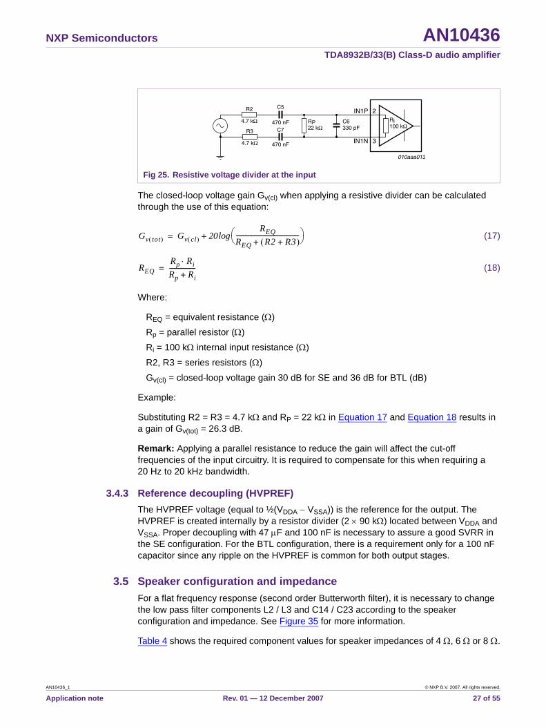
The closed-loop voltage gain Gv(cl) when applying a resistive divider can be calculated through the use of this equation:
(17)
(18)
Where:
REQ = equivalent resistance (Ω)Rp = parallel resistor (Ω)Ri = 100 kΩ internal input resistance (Ω)R2, R3 = series resistors (Ω)Gv(cl) = closed-loop voltage gain 30 dB for SE and 36 dB for BTL (dB)
Example:
Substituting R2 = R3 = 4.7 kΩ and RP = 22 kΩ in Equation 17 and Equation 18 results in a gain of Gv(tot) = 26.3 dB.
Remark: Applying a parallel resistance to reduce the gain will affect the cut-off frequencies of the input circuitry. It is required to compensate for this when requiring a 20 Hz to 20 kHz bandwidth.
3.4.3 Reference decoupling (HVPREF)The HVPREF voltage (equal to ½(VDDA − VSSA)) is the reference for the output. The HVPREF is created internally by a resistor divider (2 × 90 kΩ) located between VDDA and VSSA. Proper decoupling with 47 μF and 100 nF is necessary to assure a good SVRR in the SE configuration. For the BTL configuration, there is a requirement only for a 100 nF capacitor since any ripple on the HVPREF is common for both output stages.
3.5 Speaker configuration and impedanceFor a flat frequency response (second order Butterworth filter), it is necessary to change the low pass filter components L2 / L3 and C14 / C23 according to the speaker configuration and impedance. See Figure 35 for more information.
Table 4 shows the required component values for speaker impedances of 4 Ω, 6 Ω or 8 Ω.
Fig 25. Resistive voltage divider at the input
010aaa013
Ri100 kΩ
C5
C7470 nF
470 nF
R2
R3
4.7 kΩ
4.7 kΩ
C6330 pF
RP22 kΩ
IN1P 2
IN1N 3
Gv tot( ) Gv cl( ) 20REQ
REQ R2 R3+( )+-----------------------------------------⎝ ⎠
⎛ ⎞log+=
REQRp Ri⋅Rp Ri+-----------------=
AN10436_1 © NXP B.V. 2007. All rights reserved.
Application note Rev. 01 — 12 December 2007 27 of 55

NXP Semiconductors AN10436TDA8932B/33(B) Class-D audio amplifier
3.5.1 Filter inductorThere are two main types of inductors:
• Air coil, current independent inductance and no saturation effect.• Inductor with a magnetic core (ferrite or iron powder):
– Magnetically unshielded version (pot core).– Magnetically shielded version (pot core or toroidal core).
An air coil is used often in HiFi audio equipment, but is not very useful in mainstream audio because of the physical size.
The major benefit of an unshielded inductor is cost. However, the magnetic stray field can cause either crosstalk issues or interference with other sensitive parts inside an audio or TV system (AM-receiver, picture interference, etc.).
The benefit of the shielded magnetic inductor is that the magnetic field is captured inside the core, reducing the magnetic stray field.
The most important parameters of an inductor are:
• DC current rating to avoid magnetic saturation, causing an increase in audio distortion.
• Linearity of the inductor, causing an increase in audio distortion (especially above 1 kHz).
• DC resistance having a direct impact on efficiency.
The DC current capability needs to be high enough to avoid magnetic saturation. High peak currents are a result of saturation because the inductor tends to acts like a short. Therefore, for a proper inductor selection it is important to consider the maximum current delivered by the amplifier, and the temperature of the inductor (higher inductor temperature will decrease the saturation level). The maximum current occurs at voltage clipping and can be calculated through the use of either Equation 12 for SE configuration or Equation 13 for BTL configuration.
Example:
For a 2 × 15 W SE amplifier operating at 22 V the maximum output current is equal to 2.1 A (RDSon = 0.15 Ω and Rs = 0.05 Ω and RESR = 0.06 Ω). Therefore, it is recommended to select an inductor that retains still at least 80 % of the nominal inductance at the maximum current of 2.1 A.
Table 4. Filter component valuesConfiguration Impedance (Ω) L2 / L3 (μH) C14 / C23 (nF)SE 4 22 680
6 33 470
8 47 330
BTL 4 10 1500
6 15 1000
8 22 680
AN10436_1 © NXP B.V. 2007. All rights reserved.
Application note Rev. 01 — 12 December 2007 28 of 55

NXP Semiconductors AN10436TDA8932B/33(B) Class-D audio amplifier
Remark: Saturation will cause audio distortion and severe saturation might even damage the device.
The inductor types listed below are recommended, based on audio and EMC performance.
Remark: For EMC purposes, it is important that the inner layer (for a multiple layer winding) is attached to the switching output to minimize electrical stray fields. The inner layer (start of the winding) is indicated with a dot mark on the inductor. In this way the outside layer acts like an electrical shielding for the inner layer attached to the output with fast alternating voltages.
3.5.2 Filter capacitorA film capacitor is the best choice for audio performance. However, in most cases a ceramic SMD capacitor (NPO or X7R) will also give a satisfying performance. The voltage rating of the filter capacitor should be 25 % higher than the maximum supply voltage VP in an asymmetrical application. In a symmetrical application the voltage rating should be 25 % higher than the half the maximum supply voltage (VDDP − VSSP).
3.5.3 Zobel damping networkA zobel network is recommended in every Class-D amplifier application to damp the filter resonance (See in Figure 26 RZ and CZ). Filter resonance will occur due to the inductive behavior (LE) of the speaker voice coil.
Table 5. Recommended inductor typesBrand and type L (μH) Isat (A) Output power (W per channel) in RL = 4 Ω
TOKO 16RHBP leaded, shielded
22 4.9 25
47 3.4
TOKO 11RHBP A7503CY leaded, shielded
22 2.21 15
47 1.60
TOKO DS86C B992AS SMD, shielded
22 2.0 10
47 1.4
Sagami 7311NA leaded, shielded
22 3.4 25
47 2.3
Sagami 7E08N SMD, shielded
22 2.6 15
47 1.8
Fig 26. Zobel damping network
010aaa426
VDD
VSS
PWMLLC
CZ
RZ LE
RECLC
voice coilequivalent
circuit
AN10436_1 © NXP B.V. 2007. All rights reserved.
Application note Rev. 01 — 12 December 2007 29 of 55

NXP Semiconductors AN10436TDA8932B/33(B) Class-D audio amplifier
This zobel damping network is quite effective for a voice coil inductance LE < 10 LLC. The zobel damping network will lower the resonance peak current in the filter inductor by at least 15 % to 40 % lowering the risk of unwanted inductor saturation.
Remark: Besides inductor saturation a tweeter might also benefit from a zobel network since filter resonance can overstress the tweeter.
Table 6 contains the optimum damping resistors for different capacitor values:
A minimum zobel damping network CZ = 47 nF and RZ = 82 Ω is strongly recommended.
The optimum damping resistors are equal for 6 Ω and 8 Ω speakers when using the filter component values from Table 4, which are calculated based on fo = 40 kHz.
The resistor (RZ) should be able to at least dissipate the power when driving the amplifier with a 20 kHz unclipped sine wave.
Figure 27 shows the sine wave power dissipation (20 kHz) as a function of supply voltage.
Table 6. Damping resistors for different capacitor valuesConfiguration Speaker
impedance (Ω)LLC (μH) CLC (nF) CZ (nF) RZ (Ω)
- - - 47 82
- - - 68 56
Single ended 4 22 680 100 39
- - - 150 27
- - - 220 22
(1) CZ = 47 nF / RZ = 82 Ω(2) CZ = 68 nF / RZ = 56 Ω(3) CZ = 100 nF / RZ = 39 Ω(4) CZ = 150 nF / RZ = 27 Ω(5) CZ = 220 nF / RZ = 22 Ω
Fig 27. Power dissipation as a function of supply voltage
VP (V)10 3618 26
010aaa427
1
1.5
0.5
2
2.5
P(W)
0
(1)
(2)
(3)
(4)
(5)
AN10436_1 © NXP B.V. 2007. All rights reserved.
Application note Rev. 01 — 12 December 2007 30 of 55

NXP Semiconductors AN10436TDA8932B/33(B) Class-D audio amplifier
Remark: If the amplifier is driven at the resonance frequency (fo = 40 kHz) of the filter, the power dissipation in the resistor will rise causing the resistor to overheat.
3.5.4 Voltage clamp diodesFor a voice coil inductance LE greater than 10 times the filter inductance (LLC) the effectiveness of the zobel damping network is limited and the power dissipation in the resistor grows high, requiring bulky power resistors. In general, mostly subwoofer voice coils and HIFI multi-way speakers have such a high inductance.
Remark: Applications for which the end user is able to disconnect the speaker and operate the amplifier without speaker, might also suffer from issues of robustness because of the inductor saturation.
To avoid inductor saturation in case of high inductive load or no load, it is recommended to apply voltage clamp diodes at the output to the supply rails (see Figure 28).
Relatively cheap general purpose diodes, like the 1N4001 (VR = 50 V) or the 1N4002 (VR = 100 V) can be used for this purpose. The reverse voltage of the diode should be at least 1.2 times the supply voltage and the repetitive peak current should be 1.2 times the maximum current of the amplifier.
3.6 Single ended capacitorA single ended amplifier (Class-AB or Class-D) operating at an asymmetrical supply voltage will require an AC couple capacitor (SE capacitor) in series with the speaker. Especially for a low output power (< 25 W) it is a very cost effective solution compared to a BTL configuration. It should be noted, the SE capacitor has no major drawback on THD and audio performance in general.
The SE capacitor forms a high-pass filter with the speaker impedance. Therefore, the frequency response will roll off with 20 dB per decade below the cut-off frequency f−3dB. The cut-off frequency is equal to:
(19)
Where:
RL = load impedance (Ω).C15 (C24) = Single Ended capacitance (F) (see schematic Section 3.10).
Fig 28. Voltage clamp diodes
010aaa428
VDD
VSS
PWMLLC
Dcl2
Dcl1
CZ
RZ LE
RECLC
voice coilequivalent
circuit
f 3dB–1
2π RL C15⋅ ⋅--------------------------------=
AN10436_1 © NXP B.V. 2007. All rights reserved.
Application note Rev. 01 — 12 December 2007 31 of 55

NXP Semiconductors AN10436TDA8932B/33(B) Class-D audio amplifier
Table 7 shows the required SE capacitor values for a cut-off frequency of 60 Hz, 40 Hz and 20 Hz.
3.6.1 Voltage ratingThe voltage rating of the SE capacitor should be at least equal to the nominal supply voltage VP in the application. This because the voltage at the SE capacitor can be modulated heavily when the amplifier is driven at either a low frequency or during an overload (a short circuit across the load or to VP). In these situations the peak voltage at the SE capacitor can be almost equal to the supply voltage.
3.6.2 LifetimeThe ambient temperature and the ripple current have the greatest effect on the lifetime of the aluminium electrolytic capacitors. For lifetime considerations the SE capacitance must be able to at least handle the ripple current that is equal to the load current at ¼ rated output power. Only ¼ of the rated output power is taken into account, because it is not likely that an audio amplifier is driven continuously at rated output power over a lifetime.
The ripple current at ¼ Prated is equal to:
(20)
Where:
RL = load impedance (Ω)VP = supply voltage (V) (VDDP − VSSP)
Example:
The ripple current of an amplifier that operates at 22 V with a 4 Ω load (Prated = 15 W) is approximately 486 mA. This ripple current can be used to determine the expected lifetime of the SE capacitor. Most general purpose electrolytic capacitors (85 °C type) are capable already of handling a 486 mA ripple current.
Both the ripple current and the voltage rating must be considered to prevent the capacitor from failing.
3.7 Bootstrap capacitorA 15 nF SMD capacitor (NPO or X7R) is required to drive the high side N-channel MOSFET. The bootstrap capacitor is charged by means of an internal diode between the STAB1 (pin 25) and the BOOT1 (pin 28) at the moment that the low side MOSFET is on.
Table 7. Values SE capacitorImpedance (Ω) C15 / C24 (μF)
f−3dB = 60 Hz f−3dB = 40 Hz f−3dB = 20 Hz4 680 1000 2200
6 470 680 1500
8 330 470 1000
I1 2⁄ VP⋅
2 RL⋅--------------------- 1
4---⋅=
AN10436_1 © NXP B.V. 2007. All rights reserved.
Application note Rev. 01 — 12 December 2007 32 of 55
NXP Semiconductors AN10436TDA8932B/33(B) Class-D audio amplifier
The voltage across the bootstrap capacitor is equal to VSTAB1 − VF (forward voltage drop internal diode). Therefore a voltage rating of 16 V is sufficient for the two bootstrap capacitors.
Remark: Only the TDA8933T device requires a 1 MΩ across both bootstrap capacitors for discharging when the power stage becomes floating.
3.8 Output RC snubber networkAn RC snubber network (see schematic Section 3.10) reduces the voltage ringing at the power stage output (pin 22 and pin 27) after a voltage transition. A proper implementation of this RC snubber will improve the EMC performance (see Figure 33).
The worst case power dissipation in the snubber resistor R5 (R12) is equal to:
(21)
Where:
C9 (C29) = snubber capacitor (F)VP = supply voltage (V) (VDDP − VSSP)fosc = oscillator frequency (Hz)
Example:
Substituting C9 = 470 pF, VP = 22 V and fosc = 320 kHz in Equation 21, results in a power dissipation of 73 mW, requiring an 0805 SMD.
The voltage rating of the snubber capacitors (C9 and C26) should be 25 % higher than the maximum supply voltage in the application.
3.9 Layout recommendationsThe PCB design of an SMA is probably the most difficult part of the design, because it might affect the audio performance, the EMC performance, the thermal performance, or even the functionality of the TDA8932B/33(B).
3.9.1 EMC considerationsA double-sided PCB with plated through holes and 35 μm copper is recommended, but a single layer is feasible as well.
Figure 29 shows a proposed floor plan of the critical components that contribute to a good audio and EMC performance. The top side of this reference board is used to place the leaded components and the copper plane for thermal reasons. For more information on thermal considerations refer to Section 3.9.2.
The bottom side of the double-layer PCB is used to place the SMD components, including the TDA8932B/33(B) and the majority of the signal tracks (see Figure 30 to Figure 33).
P 1 2⁄ C9 VP( )2 2 fosc⋅ ⋅ ⋅ ⋅=
AN10436_1 © NXP B.V. 2007. All rights reserved.
Application note Rev. 01 — 12 December 2007 33 of 55

NXP Semiconductors AN10436TDA8932B/33(B) Class-D audio amplifier
Some important notes for a proper layout are summarized below:
• Input / output connectors at one side of the PCB (solid and "clean" star GND connection).
• Supply buffer capacitor (C1) close to the IC.• Filter inductor (L2, L3) close to the IC.• Filter capacitor (C14, C23) close to the output connector, together with the SE
capacitor (C15, C24).• Place the High Frequency (HF) supply decoupling capacitor close to the IC (see
Figure 30).• Place the HF decoupling capacitor STAB1/2 voltage close to the IC (see Figure 31).• Place the Bootstrap capacitor of the high-side driver close to the IC (see Figure 32).• Place the RC output snubber network close to the IC (see Figure 33).• Place the HF decoupling capacitor DREF voltage close to the IC (see Figure 33).
Fig 29. Proposed floor plan of the components
U1
FILTER INDUCTOR
SE CAPACITOR
FILTER CAPACITOR
Large signal supply and output
L2 L3
C15
C14 C23
C1
C24
Audio outputs Supply
I/O CONNECTORS AT ONE SIDE
SOLID “CLEAN” GND
Small signal input
TD
A89
32B
/33(
B)
Audio inputs
BUFFER CAPACITOR
010aaa056
AN10436_1 © NXP B.V. 2007. All rights reserved.
Application note Rev. 01 — 12 December 2007 34 of 55

NXP Semiconductors AN10436TDA8932B/33(B) Class-D audio amplifier
Remark: SMD components are on the bottom layer, viewed from the top.
Fig 30. HF decoupling supply C8, C25 Fig 31. HF decoupling STAB1/2 C17
C17
C9
C10
C432 U1 1
C18R12
C31
C30 C31617
29
26
23
20
C25
R5
15
010aaa060
C17
C9
C10
C432 U1 1
C18R12
C31
C30 C31617
29
C25
R5
15
26252423
010aaa061
Fig 32. Bootstrap capacitor high-side driver C10, C18 Fig 33. RC output snubber network
C17
C9
C10
C432 U1 1
C18R12
C31
C30 C31617
29
C25
R5
15
2825
2221
010aaa057
C17
C9
C10
C432 U1 1
C18R12
C31
C30 C31617
C25
R5
15
2926
2320
010aaa058
Fig 34. HF decoupling DREF C30
C17
C9
C10
C432 U1 1
C18R12
C31
C30 C316
C25
R5
15
18
17
010aaa059
AN10436_1 © NXP B.V. 2007. All rights reserved.
Application note Rev. 01 — 12 December 2007 35 of 55

NXP Semiconductors AN10436TDA8932B/33(B) Class-D audio amplifier
In general:
• Minimizing the current loops that carry fast alternating currents will reduce magnetic radiation.
• Minimizing the length / size of the PWM output track (fast alternating voltages) as much as possible, will prevent capacitive coupling to the environment. Otherwise this could lead to disturbances of high impedance inputs.
3.9.2 Thermal considerationsThe thermal resistance is determined by the selected SMD package, the PCB layout implementation and the airflow inside the final enclosure of the amplifier.
The TDA8932B/33(B) is available in two different thermally enhanced SMD packages:
• TDA8932BT/33T in SO32 (SOT287-1) package for reflow and wave solder process.• TDA8932BTW/33BTW in an HTSSOP32 (SOT549-1) package for reflow solder
process only.
Thermal resistance SO32 package
The SO32 package has special thermal corner leads, pins 1, 16, 17 and 32, increasing the power capability (reducing the overall Rth(j-a)) when soldered to a thermal copper plane at VSSA level. The SO package is very suitable for single layer PCB designs or PCB designs with limited space for a thermal plane. Due to the package size the SO32 is able to radiate a significant part of the heat directly into the air (thermal resistance is less depending on the heat transfer via the PCB).
The thermal resistance of a S032 package will range from about 35 K/W to 50 K/W when mounted on a single or two layer PCB (free air natural convection). Mounting a heat sink can further decrease the thermal resistance with another 15 % to 25 %.
The thermal resistance measured at the compact reference PCB (55 mm × 45 mm) with S032 package can be found in Section 5.3.
Thermal resistance HTSSOP32 package
The HTSSOP32 package has an exposed die-pad that only reduces the overall Rth(j-a) significantly when soldered to a thermal copper plane at VSSA level (thermal resistance is strongly depending on the size and the number of copper planes). This makes the HTSSOP package very suitable for multilayer PCB designs with sufficient space for two or three thermal copper planes. When applying three thermal copper planes it is even possible to reach a continuous time output power of 2 × 25 W without a heat sink.
The thermal resistance of a HTSSOP32 package will range from about 25 K/W to 55 K/W when mounted on a multilayer PCB without heat sink (free air natural convection).
Increasing the area of the thermal copper planes, the number of planes, or the copper thickness will further reduce the thermal resistance Rth(j-a) of both packages.
AN10436_1 © NXP B.V. 2007. All rights reserved.
Application note Rev. 01 — 12 December 2007 36 of 55

NXP Semiconductors AN10436TDA8932B/33(B) Class-D audio amplifier
Airflow inside enclosure
At a set level the airflow inside the enclosure will be limited compared to the situation in free air natural convection. The airflow and other heat sources close to the amplifier will influence the temperature significantly. Therefore it is always recommended (and the responsibility of the set maker) to check the temperature behavior in the final environment of the amplifier.
Remark: The TDA8932B/33(B) amplifier with the thermal foldback feature will never cause audio interruption (audio holes) due to the limited airflow and the limited presence of other heat sources close to the amplifier. Therefore this thermal foldback feature will improve the reliable of the amplifier application under extreme temperature conditions because the device itself will always stay within the Safe Operating Area (SOA).
Thermal resistance
Measured thermal resistance of both the SO32 and the HTSSOP32 reference design can be found in Section 5.3.
Thermal via’s
Thermal via’s should be applied for an optimum heat flow to other layers of the PCB to reduce the Rth(j−a). The thermal via’s should be placed close to corner leads and beyond the package for the SO32 package (see PCB layout Section 3.12).
Remark: Do not use via’s with web construction, as they will have a high thermal resistance.
Thermal calculations
To estimate the maximum junction temperature, Equation 22 can be used:
(22)
Where:
Tamb = ambient temperature (°C)P = power dissipation in U1 (W) (see Figure 50 or Figure 61, P versus PO)Rth(j−a) = thermal resistance junction ambient (K/W)
Example:
Estimation of the junction temperature at Prated (for FTC requirements).
Power dissipation P = 2.5 W (see Figure 47) at Prated = 2 × 15 W in 4 Ω. The estimated junction temperature at Tamb = 25 °C and Rth(j−a) = 44 K/W, will be Tj(max) = 135 °C (approx.) (Equation 22), staying below the TF threshold level of 140 °C.
At a Prated = 2 × 25 W in 4 Ω the TF becomes active. The TF will gradually reduce the gain and therefore reduce the long-term output power. See Section 5.3 for the output power as a function of time, when the TF becomes active. The major benefit of the TF feature is that the amplifier is not switched off when it reaches the maximum junction temperature.
Remark: Lifetime is guaranteed because the TDA8932B/33(B) stays within the safe operating area due to the TF feature.
Tj max( ) Tamb Rth j a–( ) P⋅+≈
AN10436_1 © NXP B.V. 2007. All rights reserved.
Application note Rev. 01 — 12 December 2007 37 of 55

NXP Semiconductors AN10436TDA8932B/33(B) Class-D audio amplifier
Remark: For thermal reliability and/or quality requirements on set level, an average music power of ¼ Prated is assumed. This assumption can be made because audio amplifiers are not driven continuously at the rated output power. Taking this into account, shows the major benefit of Class-D as compared to Class-AB. Class-D dissipates less at ¼ Prated and that makes it possible to comply easily with the thermal reliability and/or quality regulations with a cheap SO32 or HTSSOP32 package without a heat sink.
3.10 Schematic - revision 3.00
(1) The TDA8933T device requires a 1 MΩ in parallel with the bootstrap capacitor Cbo.
Fig 35. Schematic - version 3.00
VSSD/HW
IN1P
IN1N
DIAG
ENGAGE
POWERUP
CGND
VDDA
VSSA
OSCREF
HVPREF
INREF
IN2N
IN2P
TEST
VSSD/HW
VSSD/HW
OSCIO
HVP1
VDDP1
BOOT1
OUT1
VSSP1
STAB1
STAB2
VSSP2
OUT2
BOOT2
HVP2
VDDP2
VSSD/HW
1
2
3
4
5
6
7
8
9
10
11
13
14
12
15
IN1
C5470 nF
32
31
30
29
28
27
26
25
24
23
22
20
19
21
18
1716
C11470 nF
R10
39 kΩ
C16100nF
C4100 nF
VP
C1015 nF(1)
C9470 pF
C8100 nF
R510 Ω
C17100 nF
L3
22 μHC1815 nF(1) R12
10 Ω
C26470 pF
VPC25100 nF
VP = 10V ...35V
GND
VP
VPA
C2220 μF/35 V
C1220 μF/35 V
R1
10 Ω
U1TDA8932BT
/33T
010aaa062
HVP1
HVP2C30100 nF
C31100 nF
R2
4.7 kΩR3
4.7 kΩ
C6330 pF
S1R712 kΩ
SLEEP
ON
R6
47 kΩVPA
C2047 μF
C21100 nF
C22100 nF
C29470 nF
IN2
C27470 nF
R15
4.7 kΩ
R14
4.7 kΩ C28330 pF
R4
10 kΩ
S2
MUTE
OPERATING
1
2
1
2
VPA
R1322 Ω
C19100 nF
12C23
680 nF
C241000 μF, 25 V
HVP2
−+ OUT2 4 Ω
J4
R822 Ω
C12100 nF
12C14
680 nF
C151000 μF, 25 V
HVP1
+−
OUT1 4 Ω
J3L2
22 μH
C3100 nF
12
J1
L1
BEAD
J2
J5
AN10436_1 © NXP B.V. 2007. All rights reserved.
Application note Rev. 01 — 12 December 2007 38 of 55

NXP Semiconductors AN10436TDA8932B/33(B) Class-D audio amplifier
3.11 Bill of materials - revision 3.00
3.12 PCB layout - Revision 2Double-sided PCB (55 mm × 45 mm) with plated through holes (Ø = 0.6 mm), 35 μm copper and FR4 base material.
Table 8. Bill of materialsItem Qty Reference Part Description1 2 C1, C2 220 μF / 35 V General purpose 85 °C, Ø 8 mm
2 10 C3, C4, C12, C16, C17, C19, C21, C22, C30, C31
100 nF / 50 V SMD 0805, X7R
3 5 C5, C7, C11, C27, C29 470 nF / 16 V SMD 1206, X7R
4 2 C6, C28 330 pF / 16 V SMD 0805, X7R
5 2 C8, C25 100 nF / 50 V SMD 1206, X7R
6 2 C26, C9 470 pF / 50 V SMD 0805, X7R
7 2 C10, C18 15 nF / 16 V SMD 0805, X7R
8 2 C23, C14 680 nF / 63 V MKT-02
9 2 C24, C15 1000 μF / 25 V General purpose 85 °C Ø 12.5 mm
10 1 C20 47 μF / 25 V General purpose 85 °C Ø 6 mm
11 1 D1 LED 3 mm LED
12 3 J1, J3, J4 Screw terminal Camden Electronics CTB3551/2
13 2 J2, J5 Cinch -
14 1 L1 Bead SMD 1206, 742792115 / Würth Elektronik or BLM41PG600SN1L / Murata
15 2 L3, L2 22 μH 11RHBP / Toko A7503CY-220M
16 3 R1, R5, R12 10 R SMD 1206
17 5 R2, R3, R14, R15, R16 4.7 k SMD 0805
18 1 R4 10 k SMD 0805
19 1 R6 47 k SMD 0805
20 1 R7 12 k SMD 0805
21 2 R8, R13 22 R SMD 2512
22 1 R10 39 k SMD 0805
23 2 S2, S1 PCB switch 090320901 / Secme
24 1 U1 TDA8932BT SOT287-1 (SO32) / NXP Semiconductors
TDA8933(B)T SOT287-1 (SO32) / NXP Semiconductors
AN10436_1 © NXP B.V. 2007. All rights reserved.
Application note Rev. 01 — 12 December 2007 39 of 55
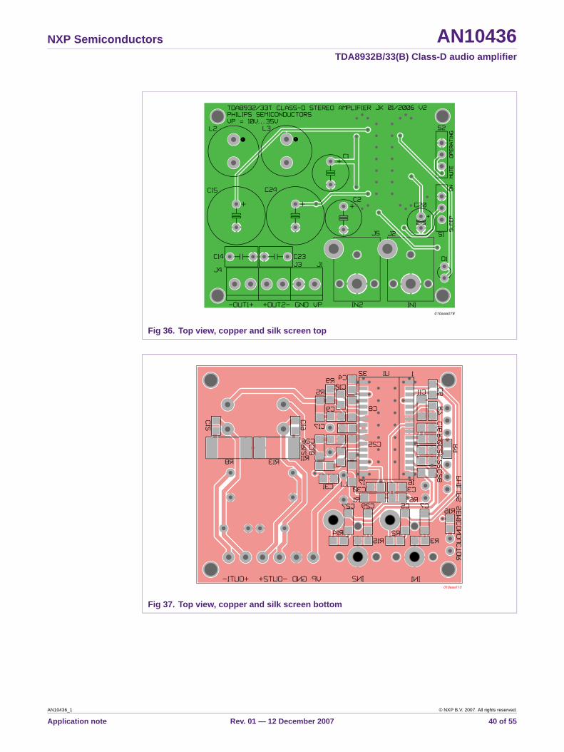
NXP Semiconductors AN10436TDA8932B/33(B) Class-D audio amplifier
Fig 36. Top view, copper and silk screen top
Fig 37. Top view, copper and silk screen bottom
010aaa078
010aaa110
AN10436_1 © NXP B.V. 2007. All rights reserved.
Application note Rev. 01 — 12 December 2007 40 of 55

NXP Semiconductors AN10436TDA8932B/33(B) Class-D audio amplifier
4. Power supply
4.1 Supply filteringA CLC phi filter (C1, L1 and C2) is used to keep the High Frequency (HF) currents locally around the amplifier (see Figure 38). Two 100 nF SMD capacitors (C8 and C25) and an electrolytic buffer capacitor (C1) should be placed close to the amplifier to minimize the area of the HF current loops to avoid emission. The ferrite bead (L1) will avoid the flow of HF currents in (mostly) large supply voltage loops. The analog voltage (VDDA) of the TDA8932B/33(B) requires an RC filter of 10 Ω (R1) and 100 nF (C3) to avoid the HF noise entering the analog controller part of the device.
4.1.1 Lifetime electrolytic capacitorThe ambient temperature and the ripple current have the greatest effect on the lifetime of the aluminium electrolytic capacitors. The output power of an amplifier is assumed often to be ¼ of the total rated output power. At a power rating of 2 × 3.75 W (¼ × 15 W) the lifetime is not an issue when general-purpose electrolytic capacitors (with a value of at least 220 μF) are used.
4.2 Supply GND connectionThe best practice to avoid any common ground path with the power supply is to leave the supply floating. The power supply should be attached to GND at the amplifier side. The differential input should be grounded at the sound processor and not at the amplifier side.
Fig 38. Supply filtering
POWERSUPPLY
L1
FERRITEBEAD
TDA8932B/33(B)
010aaa063
LPFILTER
LPFILTER
29
26
C3R110 ohm
C1C2
23
20
C8
C25
27
22
OUT 1
OUT 2
C15
C24
VDDA pin 8
HF CURRENTS
AN10436_1 © NXP B.V. 2007. All rights reserved.
Application note Rev. 01 — 12 December 2007 41 of 55

NXP Semiconductors AN10436TDA8932B/33(B) Class-D audio amplifier
4.3 Low frequency supply pumping effectA Single Ended (SE) Class-D amplifier will deliver energy back to the supply line (VP) during the negative part of the audio signal. Because most power supplies are not capable of sinking energy, the supply voltage will increase especially when driving the amplifier at low audio frequencies. This phenomenon is often called the pumping effect.
The voltage increase caused by the pumping effect depends on:
• The speaker impedance.• The supply voltage.• The audio signal frequency.• The capacitance value of the supply line.• The source/sink current of other channels (including the quiescent current of the
amplifier).• The current drawn from other circuits attached to the same supply line.
This voltage increase might trigger the OVP of the audio amplifier and/or cause incorrect control behavior of the regulated power supply.
The most effective way to overcome the pumping effect in a stereo SE application is to apply one of the input signals to the negative input to invert the phase of that particular output (see Figure 40).
Fig 39. Supply GND connection
GND
GND
POWER SUPPLYSOUND
PROCESSOR
DAC OUT
GNDFERRITE
BEAD
100nF
AMPLIFIER TDA8932B/33(B)
LPFILTER
SPEAKER
DIFFERENTIAL INPUT
SOLID GROUND PLANESTAR GROUNDAMPLIFIER SIDE
LEAVE FLOATINGFROM GROUND(OR USE RC)
010aaa079
GND
AN10436_1 © NXP B.V. 2007. All rights reserved.
Application note Rev. 01 — 12 December 2007 42 of 55

NXP Semiconductors AN10436TDA8932B/33(B) Class-D audio amplifier
With this method, OUT1 and OUT2 are out of phase to minimize the pumping effect. The inversion of one of the outputs will also halve the peak current drawn from the power supply at a low audio frequency.
Remark: Do not forget to change the polarity of the speaker connection of channel 2 to get the original phase of the signal from the speaker.
4.4 Unregulated or weak power supplyThe voltage ripple of an unregulated power supply can be quite significant, due to:
• The output impedance (load regulation).• A variation on the AC mains (line regulation).• A cross regulation in a multiple output SMPS.
Therefore, when operating from an asymmetrical supply, this voltage ripple will cause asymmetrical clipping. This might trigger also the UBP (UnBalance Protection) when the voltage ripple exceeds either −20 % or +33 % of the nominal supply voltage (see also Section 2.6.6). Therefore, any unregulated power supply (an auxiliary voltage from either an SMPS or a 50 Hz / 60 Hz transformer) might need some attention to minimize the load, the line and the cross regulation.
The voltage dip during a transient from no load condition to full load condition should be considered. The average supply current in full load for a stereo amplifier can be estimated as follows:
(23)
(24)
Where:
Po = RMS output power per channel (W)ηpo = output power efficiency, audio amplifier
Fig 40. Inverting the phase of one output and input (of channel 2)
IN1P 2
IN1N
3
TDA8932B/33(B)
IN2N 14
IN2P
15
27
22
OUT1
OUT2
C15
LPFILTER
010aaa064
C24
LPFILTER
SE: IP(avg)2 Po⋅
ηpo VP⋅-------------------=
BTL: IP(avg)Po
ηpo VP⋅-------------------=
AN10436_1 © NXP B.V. 2007. All rights reserved.
Application note Rev. 01 — 12 December 2007 43 of 55

NXP Semiconductors AN10436TDA8932B/33(B) Class-D audio amplifier
VP = supply voltage (V) (VDDP - VSSP)
Example:
A 2 × 15 W amplifier at 22 V and 89 % efficiency will draw an average supply current of 1.53 A.
Remark: For either a 50 Hz / 60 Hz transformer or a weak auxiliary supply, it might be worthwhile to consider the use of a symmetrical supply to avoid asymmetrical clipping (early clipping of the positive output voltage).
5. Performance characterization TDA8932B
5.1 Audio characterization SE
5.1.1 Performance figures SETable 9 shows the measured performance figures of the TDA8932BT two layer reference board (55 mm × 45 mm) configured in SE configuration.
VP = 22 V, RL = 2 × 4 Ω SE, fosc = 320 kHz, fi = 1 kHz, Tamb = 25 °C unless specified otherwise.
Table 9. Performance figuresSymbol Parameters Conditions / notes Min Typ Max UnitVP supply voltage operates down to UVP threshold level
operates up to OVP threshold level10[1] - 36[1] V
Po(RMS) RMS output power Continuous time output power per channel - - - -
RL = 4 Ω - - - -
THD+N = 10 % - 15.3 - W
THD+N = 0.5 % - 12.1 - W
RL = 8 Ω, VP = 30 V - - - -
THD+N = 10 % - 15.5 - W
THD+N = 0.5 % - 12.3 - W
short time output power - - - -
RL = 4 Ω, VP = 29 V - - - -
THD+N = 10 % - 26.5 - W
THD+N = 0.5 % - 21.1 - W
THD+N total harmonic distortion-plus-noise
Po = 1 W, AES17 brick wall filter 20 kHz - - - -
RL = 4 Ω - 0.015 - %
RL = 8 Ω, VP = 30 V - 0.01 - %
ηpo output power efficiency
Po = 15 W - - - -
RL = 4 Ω - 92 - %
RL = 8 Ω, VP = 30 V - 93 - %
Gv(cl) closed-loop voltage gain
Vi = 100 mVRMS, 1 kHz, Ri = 4.7 kΩ, no load - 29.2 - dB
Vi(sens) input sensitivity voltage
Prated = 2 × 15 W - 305 - mVRMS
AN10436_1 © NXP B.V. 2007. All rights reserved.
Application note Rev. 01 — 12 December 2007 44 of 55

NXP Semiconductors AN10436TDA8932B/33(B) Class-D audio amplifier
[1] It is not recommended to operate the IC at the supply boundaries (10 V or 36 V) unless the supply is regulated well.
5.1.2 Performance graphs SE
Vn(o) noise output voltage MUTE mode - 70 - μV
OPERATING mode, inputs shorted at INP, INN
- 100 - μV
S/N Signal to Noise ratio unweighted, w.r.t. VO = 7.8 VRMS - 98 - dB
B bandwidth ±3 dB, C15 = C24 = 1000 μF - 40 - 45,000 - Hz
SVRR supply voltage ripple rejection
RL = 4 Ω, Vripple = 500 mVRMS, 100 Hz, inputs shorted
- 62 - dB
RL = 8 Ω, Vripple = 500 mVRMS, 100 Hz, inputs shorted
- 60 - dB
αcs channel separation Po = 1 W, 1 kHz - 80 - dB
IP supply current total application; SLEEP mode, no load - 680 - μA
Iq quiescent current total application; MUTE / OPERATING mode - 53 - mA
Table 9. Performance figures …continued
Symbol Parameters Conditions / notes Min Typ Max Unit
VP = 22 V, 2 × 4 Ω SE(1) = 6 kHz(2) = 1 kHz(3) = 100 Hz
VP = 30 V, 2 × 8 Ω SE(1) = 6 kHz(2) = 1 kHz(3) = 100 Hz
Fig 41. THD+N as a function of output power Fig 42. THD+N as a function of output power
001aad772
10−1
10−2
10
1
102
THD+N(%)
10−3
Po (W/channel)10−2 1021010−1 1
(1)
(3)
(2)
001aad773
10−1
10−2
10
1
102
THD+N(%)
10−3
Po (W/channel)10−2 1021010−1 1
(1)
(3)
(2)
AN10436_1 © NXP B.V. 2007. All rights reserved.
Application note Rev. 01 — 12 December 2007 45 of 55
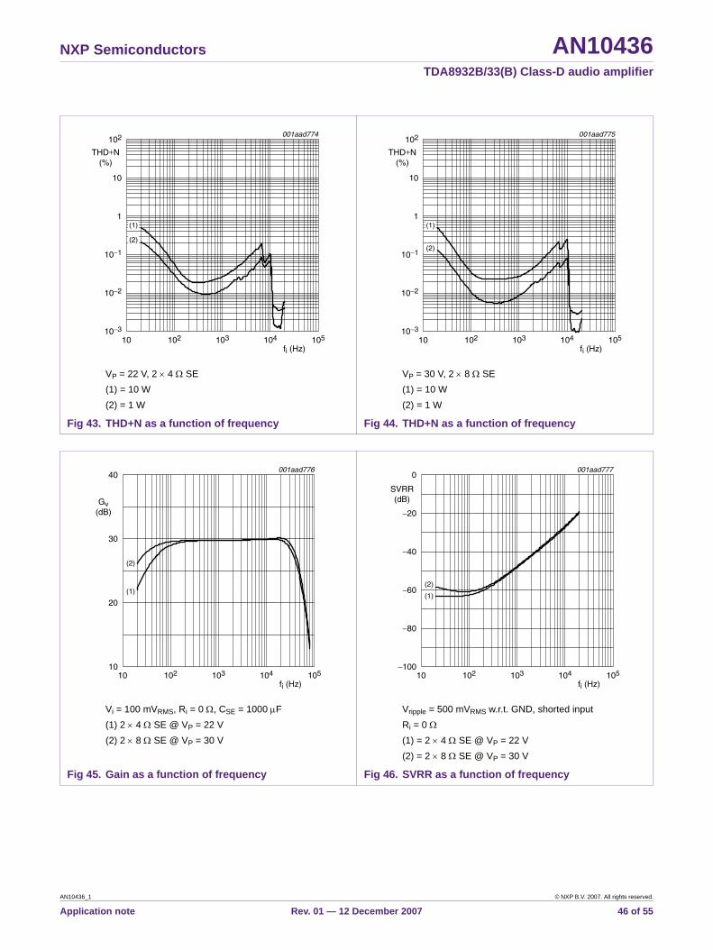
NXP Semiconductors AN10436TDA8932B/33(B) Class-D audio amplifier
VP = 22 V, 2 × 4 Ω SE(1) = 10 W(2) = 1 W
VP = 30 V, 2 × 8 Ω SE(1) = 10 W(2) = 1 W
Fig 43. THD+N as a function of frequency Fig 44. THD+N as a function of frequency
001aad774
10−1
10−2
10
1
102
THD+N(%)
10−3
fi (Hz)10 105104102 103
(1)
(2)
001aad775
10−1
10−2
10
1
102
THD+N(%)
10−3
fi (Hz)10 105104102 103
(1)
(2)
Vi = 100 mVRMS, Ri = 0 Ω, CSE = 1000 μF(1) 2 × 4 Ω SE @ VP = 22 V(2) 2 × 8 Ω SE @ VP = 30 V
Vripple = 500 mVRMS w.r.t. GND, shorted inputRi = 0 Ω(1) = 2 × 4 Ω SE @ VP = 22 V(2) = 2 × 8 Ω SE @ VP = 30 V
Fig 45. Gain as a function of frequency Fig 46. SVRR as a function of frequency
001aad776
20
30
40
Gv(dB)
10
fi (Hz)10 105104102 103
(2)
(1)
001aad777
−60
−40
−80
−20
0
SVRR(dB)
−100
fi (Hz)10 105104102 103
(2)
(1)
AN10436_1 © NXP B.V. 2007. All rights reserved.
Application note Rev. 01 — 12 December 2007 46 of 55

NXP Semiconductors AN10436TDA8932B/33(B) Class-D audio amplifier
Ri = 0 Ω(1) 2 × 4 Ω SE @ VP = 22 V(2) 2 × 8 Ω SE @ VP = 30 V
PO = 1 W, CHVPREF = 47 μF(1) = 2 × 4 Ω SE @ VP = 22 V(2) = 2 × 8 Ω SE @ VP = 30 V
Fig 47. S/N ratio as a function of output power Fig 48. Channel separation as a function of frequency
001aad778
Po (W/channel)10−2 1021010−1 1
40
80
120
S/N(dB)
0
(2)(1)
001aad779
−60
−40
−80
−20
0
αcs(dB)
−100
fi (Hz)10 105104102 103
(1)(2)
fi = 1 kHz(1) 2 × 4 Ω SE @ VP = 22 V(2) 2 × 8 Ω SE @ VP = 30 VRemark: ηpo = (2 · Po) / (2 · Po + P)
fi = 1 kHz(1) = 2 × 4 Ω SE @ VP = 22 V(2) = 2 × 8 Ω SE @ VP = 30 VRemark: Power dissipation in junction only.
Fig 49. Efficiency as a function of output power Fig 50. Power dissipation as a function of output power
Po (W/channel)0 20155 10
001aad780
40
60
20
80
100
ηpo(%)
0
(2)
(1)
001aad781
1.0
2.0
3.0
P(W)
0
Po (W/channel)10−2 1021010−1 1
(2)
(1)
AN10436_1 © NXP B.V. 2007. All rights reserved.
Application note Rev. 01 — 12 December 2007 47 of 55

NXP Semiconductors AN10436TDA8932B/33(B) Class-D audio amplifier
5.2 Audio characterization BTL
5.2.1 Performance figures BTLTable 10 shows the measured performance figures of the TDA8932BT two layer reference board (55 mm × 45 mm) configured in BTL configuration.
VP = 22 V, RL = 8 Ω BTL, fosc = 320 kHz, fi = 1 kHz, Tamb = 25 °C unless specified otherwise.
fi = 1 kHz(1) 2 × 4 Ω SE @ THD+N = 10 %(2) 2 × 4 Ω SE @ THD+N = 0.5 %(3) 2 × 8 Ω SE @ THD+N = 10 %(4) 2 × 8 Ω SE @ THD+N = 0.5 %
Fig 51. Maximum output power as a function of supply voltage
VP (V)10 3830 3414 18 22 26
001aaf886
16
8
24
32
Po(W/channel)
0
(4)
(1)
(2)
(3)
Table 10. Performance figuresSymbol Parameter Conditions/notes Min Typ Max UnitVP supply voltage operates down to UVP threshold level;
operates up to OVP threshold level10[1] - 36[1] V
Po(RMS) RMS output power RL = 8 Ω - - - -
THD+N = 10 % - 32.1 - W
THD+N = 0.5 % - 25.7 - W
RL = 4 Ω; VP = 12 V - - - -
THD+N = 10 % - 17.2 - W
THD+N = 0.5 % - 13.2 - W
THD+N total harmonic distortion-plus-noise
Po = 1 W, AES17 brick wall filter 20 kHz - - - -
RL = 8 Ω - 0.007 - %
RL = 4 Ω, VP = 12 V - 0.02 - %
ηpo output power efficiency Po = 15 W, VP = 22 V, RL = 8 Ω - 90 - %
Po = 30 W, VP = 12 V, RL = 4 Ω - 92 - %
AN10436_1 © NXP B.V. 2007. All rights reserved.
Application note Rev. 01 — 12 December 2007 48 of 55

NXP Semiconductors AN10436TDA8932B/33(B) Class-D audio amplifier
[1] It is not recommended to operate the IC at the supply boundaries (10 V or 36 V) unless the supply is regulated well.
5.2.2 Performance graphs BTL
Gv(cl) closed-loop voltage gain Vi = 100 mVRMS, 1 kHz, Ri = 4.7 kΩ, no load - 35.2 - dB
Vi(sens) input sensitivity voltage Prated = 30 W, Ri = 4.7 kΩ - 305 - mVrms
Vn(o) noise output voltage MUTE mode - 25 - μV
OPERATING mode, inputs shorted at INP, INN - 100 - μV
S/N signal-to-noise ratio unweighted, in relation to VO = 15.5 VRMS - 104 - dB
B bandwidth ±3 dB 0 to 45,000 Hz
SVRR supply voltage ripple rejection
RL = 8 W, Vripple = 500 mVRMS, 100 Hz, inputs shorted
- 77 - dB
RL = 4 W, Vripple = 500 mVRMS, 100 Hz, inputs shorted
- 77 - dB
IP supply current SLEEP mode, no load - 680 - μA
Iq quiescent current MUTE / OPERATING mode - 53 - mA
Table 10. Performance figures …continued
Symbol Parameter Conditions/notes Min Typ Max Unit
VP = 22 V, 8 Ω BTL(1) 6 kHz(2) 1 kHz(3) 100 Hz
VP = 12 V, 4 Ω BTL(1) 6 kHz(2) 1 kHz(3) 100 Hz
Fig 52. THD+N as a function of output power Fig 53. THD+N as a function of output power
001aad783
10−1
10−2
10
1
102
THD+N(%)
10−3
Po (W)10−2 1021010−1 1
(1)
(2)
(3)
001aad782
10−1
10−2
10
1
102
THD+N(%)
10−3
Po (W)10−2 1021010−1 1
(1)
(2)
(3)
AN10436_1 © NXP B.V. 2007. All rights reserved.
Application note Rev. 01 — 12 December 2007 49 of 55

NXP Semiconductors AN10436TDA8932B/33(B) Class-D audio amplifier
VP = 22 V, 8 Ω BTL(1) 10 W(2) 1 W
VP = 12 V, 4 Ω BTL(1) 10 W(2) 1 W
Fig 54. THD+N as a function of frequency Fig 55. THD+N as a function of frequency
001aae114
10−1
10−2
10
1
102
THD+N(%)
10−3
fi (Hz)10 105104102 103
(1)
(2)
001aae115
10−1
10−2
10
1
102
THD+N(%)
10−3
fi (Hz)10 105104102 103
(2)
(1)
Vi = 100 mVRMS, Ri = 0 Ω(1) 4 Ω BTL @ VP = 12 V(2) 8 Ω BTL @ VP = 22 V
Vripple = 500 mVRMS in relation to GND, shorted input, Ri = 0 Ω(1) 4 Ω BTL @ VP = 12 V(2) 8 Ω BTL @ VP = 22 V
Fig 56. Gain as a function of frequency Fig 57. SVRR as a function of frequency
001aae116
20
30
40
Gv(dB)
10
fi (Hz)10 105104102 103
(1)(2)
001aae117
−60
−40
−80
−20
0
SVRR(dB)
−100
fi (Hz)10 105104102 103
(1)
(2)
AN10436_1 © NXP B.V. 2007. All rights reserved.
Application note Rev. 01 — 12 December 2007 50 of 55

NXP Semiconductors AN10436TDA8932B/33(B) Class-D audio amplifier
Ri = 0 Ω(1) 4 Ω BTL @ VP = 12 V(2) 8 Ω BTL @ VP = 22 V
fi = 1 kHz(1) 4 Ω BTL @ THD+N = 10 %(2) 4 Ω BTL @ THD+N = 0.5 %(3) 8 Ω BTL @ THD+N = 10 %(4) 8 Ω BTL @ THD+N = 0.5 %
Fig 58. S/N ratio as a function of output power Fig 59. Maximum output power as a function of supply voltage
001aae118
Po (W)10−2 1021010−1 1
40
80
120
S/N(dB)
0
(2)
(1)
001aaf893
VP (V)10 34261814 3022
40
50
30
20
10
60
70Po(W)
0
(2)
(1)
(3)
(4)
fi = 1 kHz(1) 4 Ω BTL @ VP = 12 V(2) 8 Ω BTL @ VP = 22 VRemark: ηpo = (Po) / (Po + P)
fi = 1 kHz(1) 4 Ω BTL @ VP = 12 V(2) 8 Ω BTL @ VP = 22 VRemark: Power dissipation in junction only
Fig 60. Efficiency as a function of output power Fig 61. Power dissipation as a function of output power
001aae119
Po (W)0 302010
40
60
20
80
100
ηpo(%)
0
(2)
(1)
001aae120
1.0
2.0
3.0
P(W)
0
Po (W)10−2 1021010−1 1
(2)
(1)
AN10436_1 © NXP B.V. 2007. All rights reserved.
Application note Rev. 01 — 12 December 2007 51 of 55

NXP Semiconductors AN10436TDA8932B/33(B) Class-D audio amplifier
5.3 Thermal characterizationThe measured thermal resistance of the reference design with an SO32 package, a double-sided FR4 PCB (55 mm × 45 mm) and 35 μm copper, is equal to 44 K/W (free air and natural convection).
When the junction temperature reaches the threshold level of the Thermal Foldback (140 °C to 150 °C), it starts to reduce gradually the output power so the maximum temperature will stay always within the Safe Operating Area.
Figure 62 and Figure 63 show the TDA8932BT (S032) output power as a function of time at different supply voltages. The total output power of the device is 2 × Po, because the measurement is performed at SE configuration.
Figure 64 and Figure 65 show the TDA8932BT output power as a function of time at different supply voltages. Total output power of the device is 1 × Po because the measurement is performed at BTL configuration.
RL = 2 × 4 Ω SE; fi = 1 kHz; 2 layer SO32 application board (55 mm × 45 mm) without heat sink.(1) VP = 22 V(2) VP = 26 V(3) VP = 29 V
RL = 2 × 8 Ω SE; fi = 1 kHz; 2 layer SO32 application board (55 mm × 45 mm) without heat sink.(1) VP = 30 V(2) VP = 34 V
Fig 62. SE output power as a function of time Fig 63. SE output power as a function of time
t (s)0 600480240 360120
001aaf887
16
8
24
32
0
Po(W/channel)
(2)
(1)
(3)
t (s)0 600480240 360120
001aaf888
16
8
24
32
0
Po(W/channel)
(2)
(1)
AN10436_1 © NXP B.V. 2007. All rights reserved.
Application note Rev. 01 — 12 December 2007 52 of 55

NXP Semiconductors AN10436TDA8932B/33(B) Class-D audio amplifier
5.4 EMI characterization (FCC)The TDA8932B/33(B) reference design can comply easily with the FCC radiated emissions standards with 1 m of cable attached to all the I/Os. The spectrum analyzer is set at MAX hold and the output power is 2 × 1/8 Prated.
RL = 4 Ω; fi = 1 kHz; 2 layer SO32 application board (55 mm × 45 mm) without heat sink.(1) VP = 12 V(2) VP = 13.5 V(3) VP = 15 V
RL = 8 Ω; fi = 1 kHz; 2 layer SO32 application board (55 mm × 45 mm) without heat sink.(1) VP = 22 V(2) VP = 26 V(3) VP = 29 V
Fig 64. BTL output power as a function of time Fig 65. BTL output power as a function of time
t (s)0 600480240 360120
001aaf896
16
8
24
32
0
Po(W)
(2)
(1)
(3)
t (s)0 600480240 360120
001aaf899
20
40
60
10
30
50
Po(W)
0
(2)
(1)
(3)
Fig 66. 150 kHz to 30 MHz Fig 67. 30 MHz to 300 MHz
REF 80.0 dBμW ATTEN 10 dB
START 150 kHzRES BW 10 kHz
STOP 30.00 MHzSWP 750 msec
DISPLAY LINE50.0 dBμV
010aaa102
DL50.0dBμV
VBW 10 kHz
BATTERY
010aaa101REF 50.0 dBμW ATTEN 10 dB
START 30 MHzRES BW 100 kHz
STOP 300.0 MHzSWP 200 msec
BATTERY
DISPLAY LINE50.0 dBμV
DL50.0dBμV
VBW 30 kHz
AN10436_1 © NXP B.V. 2007. All rights reserved.
Application note Rev. 01 — 12 December 2007 53 of 55

NXP Semiconductors AN10436TDA8932B/33(B) Class-D audio amplifier
6. Legal information
6.1 DefinitionsDraft — The document is a draft version only. The content is still under internal review and subject to formal approval, which may result in modifications or additions. NXP Semiconductors does not give any representations or warranties as to the accuracy or completeness of information included herein and shall have no liability for the consequences of use of such information.
6.2 DisclaimersGeneral — Information in this document is believed to be accurate and reliable. However, NXP Semiconductors does not give any representations or warranties, expressed or implied, as to the accuracy or completeness of such information and shall have no liability for the consequences of use of such information.
Right to make changes — NXP Semiconductors reserves the right to make changes to information published in this document, including without limitation specifications and product descriptions, at any time and without notice. This document supersedes and replaces all information supplied prior to the publication hereof.
Suitability for use — NXP Semiconductors products are not designed, authorized or warranted to be suitable for use in medical, military, aircraft, space or life support equipment, nor in applications where failure or malfunction of an NXP Semiconductors product can reasonably be expected to result in personal injury, death or severe property or environmental damage. NXP Semiconductors accepts no liability for inclusion and/or use of NXP Semiconductors products in such equipment or applications and therefore such inclusion and/or use is at the customer’s own risk.
Applications — Applications that are described herein for any of these products are for illustrative purposes only. NXP Semiconductors makes no representation or warranty that such applications will be suitable for the specified use without further testing or modification.
6.3 TrademarksNotice: All referenced brands, product names, service names and trademarks are the property of their respective owners.
AN10436_1 © NXP B.V. 2007. All rights reserved.
Application note Rev. 01 — 12 December 2007 54 of 55
NXP Semiconductors AN10436TDA8932B/33(B) Class-D audio amplifier
7. Contents
1 Introduction . . . . . . . . . . . . . . . . . . . . . . . . . . . . 31.1 Block diagram. . . . . . . . . . . . . . . . . . . . . . . . . . 41.2 Fixed frequency pulse width modulated Class-D
concept . . . . . . . . . . . . . . . . . . . . . . . . . . . . . . . 41.3 Typical application circuits (simplified) . . . . . . . 51.3.1 Asymmetrical supply stereo SE configuration . 51.3.2 Symmetrical supply stereo SE configuration . . 61.3.3 Asymmetrical supply mono BTL configuration . 71.3.4 Symmetrical supply mono BTL configuration . . 82 Functional IC description . . . . . . . . . . . . . . . . . 92.1 Control inputs . . . . . . . . . . . . . . . . . . . . . . . . . . 92.1.1 Mode description . . . . . . . . . . . . . . . . . . . . . . 102.2 Half Supply Voltage (HVP) chargers. . . . . . . . 112.3 Pop free power supply on/off cycling . . . . . . . 112.3.1 Supply turn-on . . . . . . . . . . . . . . . . . . . . . . . . 112.3.2 Supply turn-off . . . . . . . . . . . . . . . . . . . . . . . . 112.4 Oscillator frequency . . . . . . . . . . . . . . . . . . . . 112.5 Device synchronization. . . . . . . . . . . . . . . . . . 122.6 Limiting and protection features . . . . . . . . . . . 132.6.1 Thermal Foldback (TF) . . . . . . . . . . . . . . . . . . 142.6.2 Cycle-by-cycle current limiting . . . . . . . . . . . . 142.6.3 Window Protection (WP). . . . . . . . . . . . . . . . . 142.6.4 UnderVoltage Protection (UVP) . . . . . . . . . . . 152.6.5 OverVoltage Protection (OVP) . . . . . . . . . . . . 152.6.6 UnBalance Protection (UBP) . . . . . . . . . . . . . 152.6.7 OverCurrent Protection (OCP) . . . . . . . . . . . . 162.6.8 OverTemperature Protection (OTP) . . . . . . . . 172.7 Pinning information. . . . . . . . . . . . . . . . . . . . . 172.8 Pin description . . . . . . . . . . . . . . . . . . . . . . . . 183 Design 2 x 5 W - 25 W audio amplifier
(asymmetrical supply) . . . . . . . . . . . . . . . . . . . 193.1 Output power estimation. . . . . . . . . . . . . . . . . 193.1.1 TDA8932B output power estimation. . . . . . . . 203.1.2 TDA8933(B) output power estimation. . . . . . . 213.2 Peak output current estimation. . . . . . . . . . . . 233.3 Control circuit . . . . . . . . . . . . . . . . . . . . . . . . . 233.4 Analog audio input . . . . . . . . . . . . . . . . . . . . . 253.4.1 Input impedance . . . . . . . . . . . . . . . . . . . . . . . 263.4.2 Gain reduction . . . . . . . . . . . . . . . . . . . . . . . . 263.4.3 Reference decoupling (HVPREF). . . . . . . . . . 273.5 Speaker configuration and impedance . . . . . . 273.5.1 Filter inductor . . . . . . . . . . . . . . . . . . . . . . . . . 283.5.2 Filter capacitor . . . . . . . . . . . . . . . . . . . . . . . . 293.5.3 Zobel damping network . . . . . . . . . . . . . . . . . 293.5.4 Voltage clamp diodes . . . . . . . . . . . . . . . . . . . 313.6 Single ended capacitor . . . . . . . . . . . . . . . . . . 313.6.1 Voltage rating . . . . . . . . . . . . . . . . . . . . . . . . . 32
3.6.2 Lifetime . . . . . . . . . . . . . . . . . . . . . . . . . . . . . 323.7 Bootstrap capacitor . . . . . . . . . . . . . . . . . . . . 323.8 Output RC snubber network . . . . . . . . . . . . . 333.9 Layout recommendations. . . . . . . . . . . . . . . . 333.9.1 EMC considerations. . . . . . . . . . . . . . . . . . . . 333.9.2 Thermal considerations . . . . . . . . . . . . . . . . . 363.10 Schematic - revision 3.00. . . . . . . . . . . . . . . . 383.11 Bill of materials - revision 3.00 . . . . . . . . . . . . 393.12 PCB layout - Revision 2 . . . . . . . . . . . . . . . . . 394 Power supply. . . . . . . . . . . . . . . . . . . . . . . . . . 414.1 Supply filtering . . . . . . . . . . . . . . . . . . . . . . . . 414.1.1 Lifetime electrolytic capacitor . . . . . . . . . . . . . 414.2 Supply GND connection. . . . . . . . . . . . . . . . . 414.3 Low frequency supply pumping effect . . . . . . 424.4 Unregulated or weak power supply . . . . . . . . 435 Performance characterization TDA8932B. . . 445.1 Audio characterization SE . . . . . . . . . . . . . . . 445.1.1 Performance figures SE. . . . . . . . . . . . . . . . . 445.1.2 Performance graphs SE. . . . . . . . . . . . . . . . . 455.2 Audio characterization BTL . . . . . . . . . . . . . . 485.2.1 Performance figures BTL . . . . . . . . . . . . . . . . 485.2.2 Performance graphs BTL. . . . . . . . . . . . . . . . 495.3 Thermal characterization . . . . . . . . . . . . . . . . 525.4 EMI characterization (FCC) . . . . . . . . . . . . . . 536 Legal information . . . . . . . . . . . . . . . . . . . . . . 546.1 Definitions . . . . . . . . . . . . . . . . . . . . . . . . . . . 546.2 Disclaimers . . . . . . . . . . . . . . . . . . . . . . . . . . 546.3 Trademarks . . . . . . . . . . . . . . . . . . . . . . . . . . 547 Contents. . . . . . . . . . . . . . . . . . . . . . . . . . . . . . 55
© NXP B.V. 2007. All rights reserved.For more information, please visit: http://www.nxp.comFor sales office addresses, please send an email to: [email protected]
Date of release: 12 December 2007Document identifier: AN10436_1
Please be aware that important notices concerning this document and the product(s)described herein, have been included in section ‘Legal information’.