an x-band schottky diode mixer in sige technology with ... · research paper an x-band schottky...
TRANSCRIPT

General rights Copyright and moral rights for the publications made accessible in the public portal are retained by the authors andor other copyright owners and it is a condition of accessing publications that users recognise and abide by the legal requirements associated with these rights
Users may download and print one copy of any publication from the public portal for the purpose of private study or research
You may not further distribute the material or use it for any profit-making activity or commercial gain
You may freely distribute the URL identifying the publication in the public portal If you believe that this document breaches copyright please contact us providing details and we will remove access to the work immediately and investigate your claim
Downloaded from orbitdtudk on Jan 15 2020
An X-band Schottky diode mixer in SiGe technology with tunable Marchand balun
Michaelsen Rasmus Schandorph Johansen Tom Keinicke Tamborg Kjeld M Zhurbenko Vitaliy YanLeiPublished inInternational Journal of Microwave and Wireless Technologies
Link to article DOI101017S1759078716001069
Publication date2017
Document VersionPeer reviewed version
Link back to DTU Orbit
Citation (APA)Michaelsen R S Johansen T K Tamborg K M Zhurbenko V amp Yan L (2017) An X-band Schottky diodemixer in SiGe technology with tunable Marchand balun International Journal of Microwave and WirelessTechnologies 9(5) 965-976 httpsdoiorg101017S1759078716001069
research paper
An X-band Schottky diode mixer in SiGetechnology with tunable Marchand balun
rasmus s michaelsen12
tom k johansen1
kjeld m tamborg2
vitaliy zhurbenko1
and lei yan1
In this paper we propose a double balanced mixer with a tunable Marchand balun The circuit is designed in a SiGe BiCMOSprocess using Schottky diodes The tunability of the Marchand balun is used to enhance critical parameters for doublebalanced mixers The local oscillator-IF isolation can be changed from ndash51 to ndash605 dB by tuning Similarly the IIP2 canbe improved from 413 to 487 dBm at 11 GHz while the input referred 1-dB compression point is kept constant at8 dBm The tuning have no influence on conversion loss which remains at 88 dB at a LO power level of 11 dBm at thecenter frequency of 11 GHz The mixer has a 3 dB bandwidth from 8 to 13 GHz covering the entire X-band The fullmixer has a size of 2050 mm times 1000 mm
Keywords Si-based devices and IC technologies Circuit design and applications
Received 16 September 2015 Revised 19 August 2016 Accepted 22 August 2016
I I N T R O D U C T I O N
FREQUENCY down conversion is a vital function in almostany microwave receiver The simplest receivers are usuallybased on the homodyne or direct conversion architecture[1] This overcomes the problem with image frequencychannel and leaves only the desired signal directly at base-band Mixers for direct conversion are also used in Dopplerradars as the direct conversion architecture gives theDoppler shift directly from the received frequency Mixersfor direct conversion have the drawback that the radio fre-quency (RF) and local oscillator (LO) frequencies are at thesame frequency thus good isolation between the ports is im-portant as filtering is not possible Also as the output fre-quency is low flicker or 1f noise might be a problem
The double balanced mixer ideally provides infinite isola-tion between all ports and is therefore a good choice to useas a mixer for direct conversion Other benefits of thedouble balanced mixer are rejection of LO noise and high lin-earity [2] The balancing circuits should to get full benefit ofthe double balanced architecture be well adjusted This ischallenging to achieve in practice due to process and manufac-turing variances
To utilize the broadband nature of the double balancedmixer the balun should also be broadband otherwise thebandwidth of the mixer will be limited The Marchandbalun [3] is in itself very broadband and it is commonly
used for this reason in a planar [4ndash6] or lumped-distributed[7ndash9] implementation In [10] we presented a Marchandbalun with tunable phase balance and in [11 12] we presenteda broad band double balanced mixer using diode connectedheterojunction bipolar transistors (HBTs) together withlumped Marchand baluns on RF and LO ports The mixerdesign presented here integrates the tunable Marchandbalun on the LO-port together with Schottky diodes for themixing core This allows to correct for any mismatcheseither in the balun design or in the mixing core itself Thisshould then enhance the benefits of practical implementationsof double balanced mixers where our focus will be on theproperties important for direct conversion mixing ie portisolation and linearity To the authorrsquos knowledge a doublebalanced ring mixer with balance corrections using atunable balun is demonstrated here for the first time
I I D E S I G N O F M I X E R W I T HT U N A B L E B A L U N
This section gives a description of the design of the circuitryFirst a description of the lumped Marchand balun design withtunable phase balance is given This will be followed by a de-scription of the full mixer circuit The theoretical treatment ofthe effect of LO balun imbalance on mixer characteristics canbe found in Appendix V
A) Marchand balun designThe broadband nature of the Marchand balun makes it anideal candidate for a double balanced mixer The idea of thetunable Marchand balun as described in [10] is to introducea tunable shunt susceptance between the two coupled
Corresponding authorRS MichaelsenEmail rsmweibeldk
1Department of Electrical Engineering Technical University of Denmark 2800Kongens Lyngby Denmark2Weibel Scientific AS 3450 Alleroslashd Denmark
1
International Journal of Microwave and Wireless Technologies page 1 of 12 Cambridge University Press and the European Microwave Association 2016doi101017S1759078716001069
httpwwwcambridgeorgcoreterms httpdxdoiorg101017S1759078716001069Downloaded from httpwwwcambridgeorgcore DTU Library - Tech Info Ctr of Denmark on 06 Oct 2016 at 085848 subject to the Cambridge Core terms of use available at
elements of the Marchand balun The tuning range Df =S21 minus S31 is given as [10]
Df asymp Z0(C4 + C2)C2 + 1
Bm (1)
where C is the coupling factor of the coupled line element Z0
is the characteristic impedance and Bm frac14 jvCm is the addedsusceptance
A typical planar Marchand balun is realized using coupledtransmission lines and the introduction of a negative suscep-tance is difficult to synthesize Instead the lumped element im-plementation [8] is suggested as this already has a capacitanceplaced where the additional susceptance is required allowingfor an effective negative susceptance by having a smaller cap-acitance than normally required The design procedurefollows the one given in [8]
B) Mixer designA diagram of the full mixer is shown in Fig 1 The mixing coreconsists of four Schottky diodes in a ring to enable the doublebalanced properties [2] When choosing the diode size theconversion-loss degradation factor [2] is a helpful guidingparameter
d = 1 + Rs
Zs+ Zsf 2
RF
Rsf 2c
(2)
where Rs is the series resistance Zs is the real diode junctionsRF input resistance and fc frac14 12pRsCj is the cutoff frequencyIncreasing the diode area will decrease the series resistancebut increase the junction capacitance Cj in such a mannerthat the cutoff frequency will decrease [13] But as the RF fre-quency is low compared to fc a larger diode will give betterconversion-loss degradation factor as the last term of (2)will be almost negligible Using Harmonic Balance simula-tions a size was found such that using single series inductorsLRF and LLO for the RF and the LO ports respectively was suf-ficient to match to 50 V This gave a diode area of 144(mm)2with corresponding series resistance of Rs frac14 19 V junctioncapacitance of Cj0 = 80 fF which results in a cutoff frequencyof fc frac14 105 GHz and a loss degradation factor of d frac14 15 dB
The IF-extraction is similar to that described in [11] Thatis the RF balun has coupling capacitors CIF to its ground con-nection allowing for the IF signal extraction It is important tomake the IF extraction symmetric as any asymmetry will affectthe balun performance On the LO side the balun will by itsgrounding ensure the IF-return path for the diode ringTable 1 gives the design parameters
C) Effect of tunable LO balunIn Appendix V the effect of LO balun imbalance on the per-formance of double balanced diode ring mixer is describedtheoretically In particular it is described how the DC offsetLO and RF leakage conversion loss and second-order inter-modulation depends upon an interaction between the LObalun imbalance (amplitude and phase imbalances) and loadmismatch The effect of load mismatch is described with aphenomenal parameter DZ The load mismatch parameter ishighly layout dependent and cannot be assessed a priori
Once the layout has been completed however it is possibleto perform an electromagnetic (EM) simulation on thelayout of the double balanced diode ring mixer circuit Thisshould provide a fair estimate of the effect of load mismatchFigure 2 shows the 3D EM preview of the Schottky diode ringfor the double balanced mixer using Momentum in ADS fromKeysight Technologies The interdigitated finger structure ofthe four Schottky diodes in the ring is clearly visual Internalports are provided at the internal anode and cathode connec-tions of each Schottky diode The EM result of the ring
Fig 1 Schematic of the double balanced mixer including RF and LO baluns
Table 1 Design parameters for the mixer circuit
Inductance Ls (nH) 102Inductive coupling K 0825Capacitive coupling Cc ( fF) 379Input matching capacitors Cs ( fF) 283Balance matching capacitor Cm ( fF) 190Matching inductor LO LLO (nH) 094Matching inductor RF LRF (nH) 094Diode area Ad (mm2) 144
2 rasmus s michaelsen et al
httpwwwcambridgeorgcoreterms httpdxdoiorg101017S1759078716001069Downloaded from httpwwwcambridgeorgcore DTU Library - Tech Info Ctr of Denmark on 06 Oct 2016 at 085848 subject to the Cambridge Core terms of use available at
structure is subsequently included into the circuit schematicfor Harmonic balance simulations With this setup it isbelieved that the load mismatch caused by the asymmetry inthe layout of the diode ring can be accurately predicted
According to the theoretical description in Appendix V theLO leakage at the IF port should not depend on the load mis-match Therefore we should expect the LO leakage to be mini-mized once the LO balun imbalance is minimized Extendingthe above EM-circuit co-simulation approach to the completemixer circuit including LO and RF baluns matching induc-tors and diode ring it is possible to predict the LO leakageas a function of phase difference between the complementaryoutputs of the LO balun This is shown in Fig 3 for an LO fre-quency of 115 GHz and LO power level of +11 dBm
As expected from our theoretical description the LO leakageis minimized for a phase difference around 1808 for the LObalun The shown phase difference ranging from 21848 to217658 corresponds to the achievable tuning range of theLO balun using the metal-oxide-semiconductor (MOS)varicap The reason that the minimum of the LO leakage isnot occurring exactly at 1808 phase difference is that the LObalun also has a small amplitude imbalance Despite this it isshown how even a rather limited tuning range can improvethe LO leakage by approximately 7 dB As described inAppendix V the second-order intermodulation is expected todepend simultaneously on interaction between the LO balun
imbalance and the load mismatch That is no second-orderintermodulation would be expected if either the LO balun im-balance or load mismatch are zero Figure 4 shows the simu-lated second-order intermodulation product at the IF portThe LO frequency is set at 114 GHz and the LO power is setat +11 dBm The two RF tones are at 115 and 11513 GHzThus the second-order intermodulation project is at 13 MHzThe power in each of the two RF tones is ndash20 dBm It is seenthat tuning the phase balance of the LO balun indeed improvesthe second-order intermodulation product Because thesecond-order intermodulation product depends on both theLO balun imbalance and the load mismatch the minimum isnot reached at exactly a phase difference of 1808 Due to thepresence of an amplitude imbalance the second-order intermo-dulation product cannot be cancelled completely
I I I E X P E R I M E N T A L R E S U L T S
In this section the experimental results are discussed Themeasurements are made on-wafer using a probe station andcalibration is used to remove losses in cables and probes
The circuit is fabricated using a SiGeC BiCMOS processfrom Innovations for High Performance Microelectronics(IHP) It is a 025 mm technology but Schottky diodes arenot a mature part of the process and may suffer from leakagecurrent Indeed characterization of fabricated Schottky diodesrevealed a significant leakage current with spreading acrosstest sites Their performance as mixer diodes howevershould not be affected too much by the leakage current Theprocess also has metal-insulator-metal (MIM) capacitorsMOS-varactors and five metal layers of which the upper twoare extra thick intended for passives or low loss interconnects
First measurements of the Marchand balun measured on aseparate breakout is presented in Section IIA) which is fol-lowed by a presentation of the measurements of the fullmixer circuit in Section IIB)
A) Marchand balun experimental resultsA break out of the circuit was manufactured with a size of700 mm times 990 mm which is shown in Fig 5 The matching
Fig 2 3D EM preview Schottky diode ring for the double balanced mixerusing Momentum in ADS from Keysight Technologies
Fig 3 LO leakage versus phase difference for the LO balun The LO frequencyis 115 GHz and the LO power is +11 dBm
Fig 4 Second-order intermodulation product at IF port versus phasedifference of the LO balun
an x-band schottky diode mixer in sige technology 3
httpwwwcambridgeorgcoreterms httpdxdoiorg101017S1759078716001069Downloaded from httpwwwcambridgeorgcore DTU Library - Tech Info Ctr of Denmark on 06 Oct 2016 at 085848 subject to the Cambridge Core terms of use available at
capacitors Cs is implemented as MIM capacitors and variablecapacitor Cm is implemented using a MOS-varactor whichcan be tuned from 035 to 10 pF The inductors Ls is implemen-ted as broad-side coupled inductor pairs using the top two metallayers for best Q-value These are diagonally offset to get thedesired inductive coupling k and capacitive coupling Cc
Figure 6 shows measurements of insertion loss reflectionand isolation of the balun structure The insertion loss isbetter than 7 dB on both channels in the range from 11 to13 GHz while having a return loss better than 145 dB Themagnitude balance is plotted in Fig 7 At the center frequencyof 12 GHz the magnitude balance can be tuned by 08 dBfrom ndash08 to 0 dB In Fig 8 the phase difference is plottedfor different bias values as a function of frequency At thecenter frequency the phase difference can be tuned by 588from 17168 to 17748 so a perfect match is not obtainablebut a large improvement of Df is still possible
B) Full mixer circuitIn this section measurements of the combined mixer circuitare discussed The circuit has a size of 2050 mm times 1000 mm
and in Fig 9 is a microphotograph of the circuit For all mea-surements the IF-frequency is 100 MHz
The conversion loss as a function of LO power at 115 GHzis plotted in Fig 10 for measurements and simulation It isalmost saturated for a LO power level of 11 dBm with a
Fig 5 Microphotograph of the tunable Marchand balun size 700 mm times990 mm
Fig 6 Insertion loss and input matching measured with tuning voltagesranging from ndash25 to 25 V
Fig 7 Measurement of magnitude imbalance with tuning voltages rangingfrom ndash25 to 25 V
Fig 8 Measurement of phase difference between output ports with tuningvoltages ranging from ndash25 to 25 V
Fig 9 Microphotograph of the mixer circuit Size 2050 mm times 1000 mm
4 rasmus s michaelsen et al
httpwwwcambridgeorgcoreterms httpdxdoiorg101017S1759078716001069Downloaded from httpwwwcambridgeorgcore DTU Library - Tech Info Ctr of Denmark on 06 Oct 2016 at 085848 subject to the Cambridge Core terms of use available at
conversion loss of 97 dB Increasing the LO power level to16 dBm will only give a small decrease in conversion loss to93 dB Thus for all other measurements the lower level of11 dBm is chosen A good agreement between measurementand simulation is observed except when the diode is drivenwith low power This is due to the diode model not being ac-curate at these power levels
The conversion loss as a function of frequency is plotted inFig 11 for measurements and simulation A good agreementbetween simulation and measurements is observed A conver-sion loss of 88 dB is obtained at 11 GHz The broadbandnature of the Marchand balun is seen and the 3-dB bandwidthis from 8 to 13 GHz covering the entire X-band and into thelower part of the Ku-band It is seen that the conversion loss isindependent of the bias voltage on the MOS varactor andthereby the LO balun imbalance This trend is in agreementwith the theoretical prediction using equation (A25) inAppendix V
Changing the tuning capacitance has a clear influence onthe LO to IF isolation as was predicted in equation (A20)in Appendix V At 11 GHz it can be changed from ndash413 dBat a bias voltage of ndash25 V to ndash487 dB at a bias voltage of
Fig 10 Conversion loss as a function of LO power
Fig 13 DC level versus tuning voltage for different frequencies
Fig 12 LO to IF isolation versus tuning voltage for different frequencies
Fig 14 IF power versus RF power at the fundamental and second-orderfrequency for different tuning voltages Extrapolated lines show IIP2Fig 11 Conversion loss as a function of frequency
an x-band schottky diode mixer in sige technology 5
httpwwwcambridgeorgcoreterms httpdxdoiorg101017S1759078716001069Downloaded from httpwwwcambridgeorgcore DTU Library - Tech Info Ctr of Denmark on 06 Oct 2016 at 085848 subject to the Cambridge Core terms of use available at
25 V In Fig 12 the LO to IF isolation is plotted as a functionof balun tuning voltage for different frequencies It is possibleto reduce the isolation more for the higher frequencies butthis is what is expected as the phase balance of the balun ismore sensitive to bias changes there and have better magni-tude balance as shown in Figs 7 and 8
The RFndashIF isolation is also constant due to the fact that themain contributing mechanism to the leakage is unbalance inthe RF-balun which remains constant
In Fig 13 the DC offset is plotted versus the tuning voltageIt is possible to change the DC offset by a few mV but there isa larger offset of around 9 mV which cannot be completelyremoved As would be expected there is a larger swing forthe higher frequencies as the balun is more sensitive hereApart from disturbing the following circuitry the DC offsetis also unwanted as it increases the flicker noise level [14]
The linearity is plotted in Fig 14 The 1 dB compressionpoint is measured to be at 8 dBm RF input power
Intermodulation is measured with two RF tones at frequen-cies of 115 and 11513 GHz For the measurements thesecond-order product at 13 MHz and the third-orderproduct at 74 MHz is chosen The LO frequency is114 GHz Isolators are placed after the signal generators toavoid leakage and intermodulation of the signals before theyare applied to the mixer Attenuation is added to the outputof the mixer to avoid measuring the non-linearity of the spec-trum analyzer [15] From Fig 14 the IIP2 can be read as theextrapolated values to be 455 488 and 571 dBm for biaslevels of ndash25 0 and 25 V respectively giving a 116 dBtuning range of IIP2 The curve corresponding to the 25 Vbias point has a steeper slope for the last couple of pointswhich could be a fourth-order phenomenon as the one thatwas observed in [11] The IIP3 is likewise found to be20 dBm for all bias levels This is according to the theoryexplained in Appendix V where it was shown that thesecond-order intermodulation is sensitive to small changesin the balance according to equation (A26) whereas thethird-order intermodulation is not according to equation(A28) Thus it is experimentally shown that a tunable baluncan enhance the properties of the double balanced mixer byincreasing the LOndashIF isolation and the IIP2
In Table 2 the mixer is compared with other state-of-the-artdirect conversion mixers reported in the open literature Aswould be expected from a SiGe technology it is clear that ifone wants an extremely linear circuit an active topology isnot suitable Of course the active topology comes with thebenefit of having 45 dB gain compared with 288 dB orworse for the passive diode-based topologies The 1 dB com-pression point is lower than what is reported for [17] and[11] but these also exhibit more loss
The best IIP2 is achieved by [11] but after tuning ourcircuit is close to this and on par with [17]
An explanation for the poorer isolation and intermodula-tion is that a perfect balance is not obtained anywhere inthe tuning range of the balun For the mixer reported in[11] the inherent balun balance is believed to be extraordinarygood which however can generally not be assured in all prac-tical cases
I V C O N C L U S I O N
We have presented a Schottky mixer design in a SiGe technol-ogy with a balun which is tunable to reduce leakage andenhance linearity A breakout of the balun was measuredThe full mixer has a size of 2050 mmtimes 1000 mm The centerfrequency of the mixer is 11 GHz Here it has a conversionloss of ndash88 dB with a LO power level of 11 dBm The 3-dBbandwidth is from 8 to 13 GHz more than the entireX-band The conversion loss is constant over the tuningrange The LOndashIF isolation on the other hand can changefrom 413 to 487 dBm at 11 GHz The IIP2 can be improvedby the tuning from 455 to 571 dBm while the 1-dB compres-sion point and IIP3 is kept constant at 67 and 20 dBm
R E F E R E N C E S
[1] Razavi B Design considerations for direct-conversion receiversIEEE Trans Circuits Syst II Analog Digital Signal Process 44 (6)(1997) 428ndash435
[2] Maas SA Microwave Mixers 2nd ed Artec House BostonLondon 1993
[3] Marchand N Transmission-line conversion transformersElectronics 17 (1944) 142ndash145
[4] Zhang Z-Y Guo Y-X Ong L Chia MYW A new planarMarchand balun in Int Microwave Symp (MTT-S) Long BeachCA USA 2005
[5] Ang KS Robertson ID Elgaid K Thayne IG 40 to 90 GHzimpedance-transforming CPW Marchand balun in IEEEMTTS Int Microwave Symp Digest Boston MA USA 20001141ndash1144
[6] Ma T-G Wang C-C Lai C-H Miniaturized distributedMarchand balun using coupled synthesized CPWs IEEE MicrowWireless Compon Lett 21 (2011) 188ndash190
[7] Ang KS Leong YC Lee CH Analysis and design of miniatur-ized lumped-distributed impedance-transforming baluns IEEETrans Microw Theory Tech 51 (2003) 1009ndash1017
Table 2 Comparison between this work and recent reported direct conversion mixers
References Technology Topology Frequency(GHz)
CG(dB)
LO-power(dBm)
LO-IFRF-IFLO-RFisolation (dB)
IP1 dB
(dBm)IIP2(dBm)
[16] SiGe HBT Active doublebal
18 45 21 ndashndash31 2122 203
[17] SiC Schottky Double bal 24 212 24 30 7ndash 23 58[11] SiGe
HBT-diodeDouble bal 85 298 15 554058 12 66
[Thiswork]
SiGe Schottky Double bal 11 288 11 60535537 8 45ndash57
6 rasmus s michaelsen et al
httpwwwcambridgeorgcoreterms httpdxdoiorg101017S1759078716001069Downloaded from httpwwwcambridgeorgcore DTU Library - Tech Info Ctr of Denmark on 06 Oct 2016 at 085848 subject to the Cambridge Core terms of use available at
[8] Johansen TK Krozer V Analysis and Design of Lumped ElementMarchand Baluns In Mikon Conf Proc Wroclaw Poland 2008
[9] Miao X Zhang W Geng Y Chen X Ma R Gao J Design ofcompact frequency-tuned microstrip balun IEEE AntennasWireless Propag Lett 9 (2010) 686ndash688
[10] Michaelsen R Johansen T Tamborg K Zhurbenko V a modi-fied Marchand balun configuration with tunable phase balanceIEEE Microw Wireless Compon Lett 23 (2013) 66ndash68
[11] Michaelsen R Johansen T Tamborg K Zhurbenko V Design ofa broadband passive X-band double-balanced mixer in SiGe HBTtechnology Int J Microw Wireless Technol 6 (2014) 235ndash242
[12] Michaelsen RS Johansen TK Kjeld T Vitaliy Z A PassiveX-Band Double Balanced Mixer Utilizing Diode Connected SiGeHBTs 8th European Microwave Integrated Circuit Conf(EuMIC) Nuremberg Germany 2013
[13] Rassel RM et al Schottky barrier diodes for millimeter wave sige-bicmos applications in Proc of the 2006 BipolarBicmos Circuitsand Technology Meeting Maastricht Netherlands 2006
[14] Michaelsen R Johansen T Tamborg K Investigation ofLO-leakage cancellation and DC-offset influence on flicker-noisein X-band mixers in 7th European Microwave Integrated CircuitConf (EuMIC) Amsterdam Netherlands 2012
[15] Maas SA Nonlinear Microwave and RF Circuits 2nd ed ArtecHouse 2003
[16] Wang Y Duster JS Kornegay KT Park H Laskar J An18 GHz low noise high linearity active mixer in SiGe in ProcIEEE Int Symp Circuits and Systems 2005
[17] Sudow M Andersson K Nilsson P-A Rorsman N A highlylinear double balanced Schottky diode S-band mixer IEEEMicrow Wireless Compon Lett 16 (2006) 336ndash338
[18] Michaelsen R Johansen T Krozer V Design of a x4 subharmonicsub-millimeter wave diode mixer based on an analytic expression forsmall-signal conversion admittance parameters in 2013 Microwaveand Optoelectronics Conf (IMOC) Rio de Janeiro Brazil 2013
[19] Abramowitz M Stegun IA Handbook of MathematicalFunctions Dover Publications Washington DC USA 1968
Rasmus S Michaelsen received theMSc and PhD degrees in ElectricalEngineering from the Technical Univer-sity of Denmark Denmark in 2010 and2016 repectively In 2009 he joinedWeibel Scientific AS designing andtesting X-band microwave componentsand later as MMIC design engineer In2010 he was on an external stay at Phy-
sikalisches Institut Johann Wolfgang Goethe-UniversitatFrankfurt am Main Germany His current research interestsinclude microwave monolithic integrated circuit (MMIC)design nonlinear circuits flicker noise and direct conversionreceiver circuits
Tom K Johansen received his MS andPhD degrees in Electrical Engineeringfrom the Technical University of Den-mark Denmark in 1999 and 2003 re-spectively In 1999 he joined theElectromagnetic Systems group DTUElektro Technical University of Den-mark Denmark where he is currentlyan Associate Professor From September
2001 to March 2002 he was a Visiting scholar at the centerfor wireless communication University of San Diego Califor-nia Ca From November 2012 to February 2013 he spent a sab-batical at the Ferdinand Braun Institute (FBH) in BerlinGermany His research areas include the modeling of HBT de-vices microwave millimeter-wave and sub-millimeter-waveintegrated circuit design
Kjeld M Tamborg was born in KastrupDenmark in 1966 He received his MScdegree in Electronics from the TechnicalUniversity of Denmark (DTU) in 1990He was in 1990 hired by Weibel ScientificAS Alleroslashd Denmark where he is stillworking Since 2007 he has been respon-sible for the product Weibel radar an-tenna heads and components inside
During his work he has developed micro strip antenna ele-ments low noise amplifiers power amplifiers mixers oscilla-tors and many other components for X-band radar
Vitaliy Zhurbenko received the MScdegree from the Kharkiv National Univer-sity of Radio Electronics in 2001 and thePhD degree from the Technical Univer-sity of Denmark in 2008 all in ElectricalEngineering From November 2000 toJune 2005 he was a metrology engineerwith the Laboratory of Metrology Khar-kiv Ukraine In 2005 he joined the Tech-
nical University of Denmark where he is currently an AssociateProfessor His current research interests include microwave andmillimeter wave devices and integrated circuits for instrumenta-tion applications microwave and millimeter wave sensing forbiomedical and security applications microwave imaging andradars antenna and passive circuit design and characterization
Lei Yan was born in Beijing China in1980 He received the BE degree inElectronics Engineering from XirsquodianUniversity China in 1998 He receivedthe MSc and PhD degrees in ElectricalEngineering department of Technicaluniversity of Denmark in 2007 and2012 respectively His previous researchinterests include wideband MMIC de-
signs low noise amplifiers mixer and mm-wave power amp-lifier Since 2012 he joined the photonic-componentdepartment in Fraunhofer Heinrich-Hertz-Institut at Berlinfor IC development in optical communication field
an x-band schottky diode mixer in sige technology 7
httpwwwcambridgeorgcoreterms httpdxdoiorg101017S1759078716001069Downloaded from httpwwwcambridgeorgcore DTU Library - Tech Info Ctr of Denmark on 06 Oct 2016 at 085848 subject to the Cambridge Core terms of use available at
A P P E N D I X
V N O N - I D E A L D O U B L E B A L A N C E DM I X E R T H E O R Y
This section will give a theoretical description of the behaviorof double balanced mixers in the case of non-ideal baluns Themain focus will be on DC offset port isolation and the inter-modulation products First we investigate the large signal con-ditions for the LO-voltage This is followed by an analysis ofthe behavior of the ring mixer due to unbalance The analysistakes the time-varying nature of the diodes non-linear con-ductances under the influence of LO balun imbalances intoaccount Thus it will be possible to identify the mechanismsresponsible for DC offset LO and RF leakage conversionloss and second-order intermodulation products
The diode ring which will be used as the core of the doublebalanced mixer is depicted in Fig 15 The current througheach Schottky diode is given by
Idn = Is expVdn
hVT
( )minus 1
( ) (A1)
where Is is the saturation current Vdn is the large signal diodevoltage across diode n h is the ideality factor and VT is thethermal voltage
To find the LO-voltage across a single diode in the diodering we look at the left and right half-circuit independentlyThe half-circuit is shown in Fig 16 where the impedanceZm is a combination of IF RF load and embeddingnetwork Using the definitions on the figure we have the fol-lowing voltage relation
Va = Vd1 + ZmIm (A2)
Vb = minusVd2 + ZmIm (A3)
where Im = ia + ib = Is expVd1
hVT
( )minus exp
Vd2
hVT
( )( ) (A4)
The signals Va and Vb can be given as
Va = VLO 1 minus DA2
( )cos vLOt minus Df
2
( ) (A5)
Vb = minusVLO 1 + DA2
( )cos vLOt + Df
2
( ) (A6)
where we have introduced a phase error Df and a amplitudeerror DA This allows us to investigate the consequences ofimbalance on circuit performance We also introduce a loadimbalance on the IF load given as Zmleft = Zm(1 + (DZ2))and Zmright = Zm(1 minus (DZ2)) for the left and right half cir-cuits respectively The term ZmIm from (A2) which will con-tribute to a voltage difference across the two diodes isapproximated by the term (1 + AZ(1 minus (DZ2))) where AZ
is a function of the amplitude and phase balance This termreduces to zero if the amplitude and phase balance are bothzero Then the large signal diode voltages can be approxi-mated to
Vd1 = VLO 1 minusDA2
( )cos vLOt minus Df
2
( )1 minus AZ 1 + DZ
2
( )( )
(A7a)
Vd2 = VLO 1 +DA2
( )cos vLOt + Df
2
( )1 + AZ 1 + DZ
2
( )( )
(A7b)
Vd3 =minusVLO 1+DA2
( )cos vLOt+Df
2
( )1+AZ 1minusDZ
2
( )( )
(A7c)Fig 15 Schottky diode ring
Fig 16 Half circuit of diode ring left side
8 rasmus s michaelsen et al
httpwwwcambridgeorgcoreterms httpdxdoiorg101017S1759078716001069Downloaded from httpwwwcambridgeorgcore DTU Library - Tech Info Ctr of Denmark on 06 Oct 2016 at 085848 subject to the Cambridge Core terms of use available at
Vd4 =minusVLO 1minusDA2
( )cos vLOtminusDf
2
( )1minusAZ 1minusDZ
2
( )( )
(A7d)
From Fig 15 we have
I1 = Id1 minus Id2 (A8)
I2 = Id3 minus Id4 (A9)
Summing these gives the currents at the IF port and the differ-ence gives the current at the RF port
IIF = I1 + I2 (A10)
IRF = I1 minus I2 (A11)
The current through each diode as a function of RF voltagecan be expressed as a Taylor series taken around the largesignal LO voltage
Idn (t) = I0dn(t) + g1dn
(t)v + g2dn(t)v2 + g3dn
(t)v3 + middot middot middot (A12)
where dn denotes the diode number n I0dn= Id(V)|V=Vdn
g1 = dId(V)dV
∣∣V=Vdn
and g2 = 12d2Id(V)dV2∣∣
V=Vdn
Using (A12) we will investigate how the DC offset LO andRF leakage conversion loss and second-order intermodula-tion depends on the unbalances For each diode the currentwill be given as
Id1 = I0d1(t) minus g1d1
(t)vRF + g2d1(t)v2
RF minus g3d1(t)v3
RF (A13a)
Id2 = I0d2(t) + g1d2
(t)vRF + g2d2(t)v2
RF + g3d2(t)v3
RF (A13b)
Id3 = I0d3(t) + g1d3
(t)vRF + g2d3(t)v2
RF + g3d3(t)v3
RF (A13c)
Id4 = I0d4(t) minus g1d4
(t)vRF + g2d4(t)v2
RF minus g3d1(t)v3
RF (A13d)
A) DC offset from LO driveFrom (A12) a DC contribution comes from the first term I0(t)or the even ordered terms for vLO = vRF In this section wewill only look at the DC that comes from the I0(t) term inSection VE) we look at the DC term coming from higherorders It should be mentioned that other mechanisms canalso add to the DC offset such as LO-self mixing due to aparasitic path from the LO port to the RF port before themixer core [14] The zero-order Fourier coefficient corre-sponds to the DC-current through each diode The zero-orderFourier coefficient I0(t) corresponds to the DC-current
through each diode can be found as [18]
I00d1
= Is I0VLO(1 minus (DA2))(1 minus AZ(1 + (DZ2)))
hVT
( )minus 1
[ ]
(A14a)
I00d2
= Is I0VLO(1 + (DA2))(1 + AZ(1 + (DZ2)))
hVT
( )minus 1
[ ]
(A14b)
I00d3
= Is I0VLO(1 + (DA2))(1 + AZ(1 minus (DZ2)))
hVT
( )minus 1
[ ]
(A14c)
I00d4
= Is I0VLO(1 minus (DA2))(1 minus AZ(1 minus (DZ2)))
hVT
( )minus 1
[ ]
(A14d)
where I0(x) is the modified Bessel function of order 0 and ar-gument x As the deviations are all small linearizing will givebetter insight First we reformulate the nominator in (A14a)
VLO 1 minus DA2
( )1 minus AZ 1 minus DZ
2
( )( )= VLO 1 + a( ) (A15)
where a = minusDA2 minus AZ(1 minus (DZ2)) + DA(2)AZ(1 minus (DZ2)) Similar relations can be formulated for (A15) through(A14d) Then linearizing the Bessel function around VLOfor small deviations of a using [9628] in [19] gives
I0VLO(1 + a)
hVT
( )= I0
VLO
hVT
( )+ VLO
hVTI1
VLO
hVT
( )a (A16)
where I1(x) is the modified Bessel function of first order andargument x Using this relation in (A14a) through (A14d)inserting them into (A8) and (A9) and then into (A10) weget
IIF = I00d1
minus I00d2
+ I00d3
minus I00d4
= minusIsVLO
hVTI1
VLO
hVT
( )4AZ
DZ2
(A17)
This shows that a DC contribution comes directly from theLO signal in the mixer core due to load mismatch (DZ ) to-gether with LO balun imbalance (contained in AZ) For aproperly designed circuit this contribution to the DC offsetshould be of a little concern
B) LO leakageThe LO leakage is found as the fundamental current runningthrough the diodes to the IF port corresponding to the first-order term of the Fourier series of I0dn The first-order Fourier
an x-band schottky diode mixer in sige technology 9
httpwwwcambridgeorgcoreterms httpdxdoiorg101017S1759078716001069Downloaded from httpwwwcambridgeorgcore DTU Library - Tech Info Ctr of Denmark on 06 Oct 2016 at 085848 subject to the Cambridge Core terms of use available at
coefficients of I0dn can be found as [18]
I10d1
= Is
I1VLO(1 minus (DA2))(1 minus AZ(1 + (DZ2)))
hVT
( )
times exp minusjDf
2
( )minus 1
⎡⎢⎢⎣
⎤⎥⎥⎦
(A18a)
I10d2
= Is
I1VLO(1 + (DA2))(1 + AZ(1 + (DZ2)))
hVT
( )
times exp jDf
2
( )minus 1
⎡⎢⎢⎣
⎤⎥⎥⎦
(A18b)
I10d3
= minusIs
I1VLO(1 + (DA2))(1 + AZ(1 minus (DZ2)))
hVT
( )
times exp jDf
2
( )minus 1
⎡⎢⎢⎣
⎤⎥⎥⎦
(A18c)
I10d4
= minusIs
I1VLO(1 minus (DA2))(1 minus AZ(1 minus (DZ2)))
hVT
( )
times exp minusjDf
2
( )minus 1
⎡⎢⎢⎣
⎤⎥⎥⎦
(A18d)
The term exp(j(Df2)) is due to the phase mismatch becausewhen calculating the nrsquoth Fourier coefficient this appears asthe modified Bessel function times a factor exp jn(Df2)
( )[18] Linearizing the modified Bessel function of first orderaround VLO that is for small deviations using [9628] in[19] gives
I1VLO(1 + a)
hVT
( )= I1
VLO
hVT
( )+ 1
2VLO
hVT
times I0VLO
hVT
( )+ I2
VLO
hVT
( )( )a
(A19)
Using this relation in (A14a) through (A14d) inserting theminto (A8) and (A9) and then into (A10) we get
IIF =minus 2jIsVLO
hVTI0
VLO
hVT
( )+ I2
VLO
hVT
( )( )
times cosDf
2
( )AZ + DA
2
( )+ j sin
Df
2
( )DA2
AZ
[ ]
(A20)
From (A20) it is seen that there is a strong connectionbetween balun imbalances and the LO leakage but no depend-ence on load mismatch
C) RF leakageThe second term of (A12) describes the linear behavior of theRF current The RF leakage is found as the zeroth-orderFourier coefficient of g1dn
(t) This can be evaluated as [18]
G01d1
= Is
hVTI0
VLO(1 minus (DA2))(1 minus AZ(1 + (DZ2)))hVT
( )
(A21a)
G01d2
= Is
hVTI0
VLO(1 + (DA2))(1 + AZ(1 + (DZ2)))hVT
( )
(A21b)
G01d3
= Is
hVTI0
VLO(1 + (DA2))(1 + AZ 1 minus (DZ2)( )
)hVT
( )
(A21c)
G01d4
= Is
hVTI0
VLO(1 minus (DA2))(1 minus AZ(1 minus (DZ2)))hVT
( )
(A21d)
Linearizing the Bessel function and using equations (A13)through (A14) we get
IIF = (minusG01d1
minus G01d2
+ G01d3
+ G01d4)vRF
= minus4vRFIsVLO
(hVT )2 I1VLO
hVT
( )DA2
AZDZ2
(A22)
As observed from (A22) an imbalance in the LO balun willresult in a RF leakage if there is also simultaneously a mis-match in the IF-load This is not to say that this is the onlyway a RF-leak can occur an imbalance in the RF-balun hasa high impact on the RF-leakage but this is outside thescope of this analysis
D) Conversion lossThe desired mixing product at the IF frequency is found whenthe RF signal is multiplied with the fundamental tone ofg1dn
(t) The contribution can be evaluated from the first-orderFourier coefficients as
G11d1
= Is
hVTI1
VLO(1 minus (DA2))(1 minus AZ(1 + (DZ2)))hVT
( )
times exp minusjDf
2
( )
(A23a)
10 rasmus s michaelsen et al
httpwwwcambridgeorgcoreterms httpdxdoiorg101017S1759078716001069Downloaded from httpwwwcambridgeorgcore DTU Library - Tech Info Ctr of Denmark on 06 Oct 2016 at 085848 subject to the Cambridge Core terms of use available at
G11d2
= Is
hVTI1
VLO(1 + (DA2))(1 + AZ(1 + (DZ2)))hVT
( )
times exp jDf
2
( )
(A23b)
G11d3
= minus Is
hVTI1
VLO(1 + (DA2))(1 + AZ(1 minus (DZ2)))hVT
( )
times exp jDf
2
( )
(A23c)
G11d4
= minus Is
hVTI1
VLO(1 minus (DA2))(1 minus AZ(1 minus (DZ2)))hVT
( )
times exp minusjDf
2
( )
(A23d)
Linearizing the Bessel function and using equations (A13)through (A14) we get
IIF = (minusG11d1
minus G11d2
+ G11d3
+ G11d4)vRF
= minus4vRFIs
hVTI1
VLO
hVT
( )cos
Df
2
( )[
+ 12
VLO
hVTI2
VLO
hVT
( )+ I0
VLO
hVT
( )( )
times AZDA2
cosDf
2
( )+ j AZ + DA
2
( )sin
Df
2
( )( )]
(A24)
The conversion loss is inversely proportional to the IF currentTherefore it is observed that the conversion loss is notaffected much by the phase imbalance as cos(Df2) asymp 1and the second term is negligible under the assumption ofsmall deviations
E) Second-order intermodulationThe third term of (A12) describes the second-order behaviorof the RF current The zeroth-order Fourier coefficient ofg2dn
(t) gives rise to the second-order intermodulation andDC-contribution from the RF signal The Fourier coefficientcan be found as [18]
G02d1= Is
2(hVT )2 times I0VLO(1minus(DA2))(1minusAZ(1+(DZ2)))
hVT
( )
(A25a)
G02d2= Is
2(hVT )2 times I0VLO(1+(DA2))(1+AZ(1+(DZ2)))
hVT
( )
(A25b)
G02d3= Is
2(hVT )2times I0VLO(1+(DA2))(1+AZ(1minus(DZ2)))
hVT
( )
(A25c)
G02d4= Is
2(hVT )2 times I0VLO(1minus(DA2))(1minusAZ(1minus(DZ2)))
hVT
( )
(A25d)
Again by linearizing the Bessel function and using equations(A13) through (A14) we get
IIF = G02d1
minusG02d2
+G02d3
minusG02d4
( )v2
RF
=minus2VLOIs
(hVT )3 I1VLO
hVT
( )AZ
DZ2
v2RF
(A26)
From (A26) we see that second-order intermodulation pro-ducts will arise if there is a load mismatch together with aLO-balun imbalance
F) Third-order intermodulationThe fourth term of (A12) describes the third-order behaviorof the RF current To mix the frequencies to be near the IF fre-quency it is neccessary for the third-order RF to mix with theLO ie it is the first-order Fourier coefficient of g2dn
(t) whichgive rise to the third-order intermodulation from the RFsignal The Fourier coefficient can be found as [18]
G13d1
= Is
6(hVT )3 I1VLO(1 minus (DA2))(1 minus AZ(1 + (DZ2)))
hVT
( )
times exp minusjDf
2
( )
(A27a)
G13d2
= Is
6(hVT )3 I1VLO(1 + (DA2))(1 + AZ(1 + (DZ2)))
hVT
( )
times exp jDf
2
( )
(A27b)
G13d3
=minus Is
6(hVT )3 I1VLO(1+(DA2))(1+AZ(1minus(DZ2)))
hVT
( )
times exp jDf
2
( )
(A27c)
G13d4
=minus Is
6(hVT )3 I1VLO(1minus(DA2))(1minusAZ(1minus(DZ2)))
hVT
( )
times exp minusjDf
2
( )
(A27d)
an x-band schottky diode mixer in sige technology 11
httpwwwcambridgeorgcoreterms httpdxdoiorg101017S1759078716001069Downloaded from httpwwwcambridgeorgcore DTU Library - Tech Info Ctr of Denmark on 06 Oct 2016 at 085848 subject to the Cambridge Core terms of use available at
Linearizing the Bessel function and using equations (A13)through (A14) we get
IIF =(minus G1
3d1minus G1
3d2+ G1
3d3+ G1
3d4
)v3
RF
= minus 23
vRFIs
(hVT )3
I1VLO
hVT
( )cos
Df
2
( )+ 1
2VLO
hVT
I2VLO
hVT
( )+ I0
VLO
hVT
( )( )⎡⎢⎢⎣
times AZDA2
cosDf
2
( )+ j AZ + DA
2
( )sin
Df
2
( )( )]
(A28)
It is observed that the third-order intermodulation is notaffected much by the phase imbalance as cos(Df2) asymp 1and the second term is negligible under the assumption ofsmall deviations just like the conversion loss
12 rasmus s michaelsen et al
httpwwwcambridgeorgcoreterms httpdxdoiorg101017S1759078716001069Downloaded from httpwwwcambridgeorgcore DTU Library - Tech Info Ctr of Denmark on 06 Oct 2016 at 085848 subject to the Cambridge Core terms of use available at
- An X-band Schottky diode mixer in SiGe technology with tunable Marchand balun
-
- INTRODUCTION
- DESIGN OF MIXER WITH TUNABLE BALUN
-
- Marchand balun design
- Mixer design
- Effect of tunable LO balun
-
- EXPERIMENTAL RESULTS
-
- Marchand balun experimental results
- Full mixer circuit
-
- CONCLUSION
- APPENDIX
- NON-amph 014IDEAL DOUBLE BALANCED MIXER THEORYampshow [AQ ID=Q12]
-
- DC offset from LO drive
- LO leakage
- RF leakage
- Conversion loss
- E) Second-amph 014order intermodulation
- F) Third-amph 014order intermodulation
-
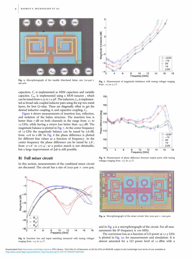
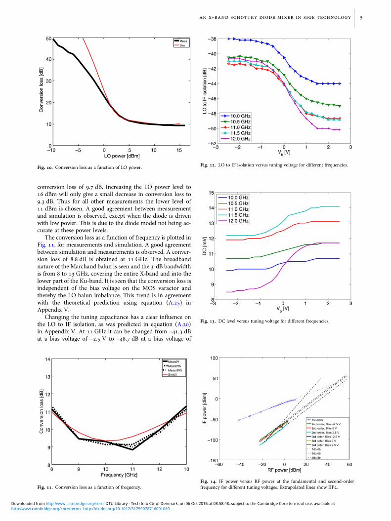
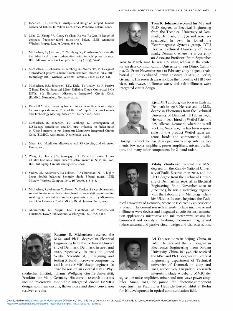