an energy-efficient solution from freescale mc9s08mm128...
TRANSCRIPT

© Freescale Semiconductor, Inc., 2009-2010. All rights reserved.
Freescale reserves the right to change the detail specifications as may be required to permit improvements in the design of its products.
80-LQFP 12mm x 12mm64-LQFP 10mm x 10mm 81-MapBGA 10mm x10mm
8-Bit HCS08 Central Processor Unit (CPU)– Up to 48-MHz CPU above 2.4 V, 40 MHz CPU above 2.1 V, and
20 MHz CPU above 1.8 V across temperature of -40°C to 105°C – HCS08 instruction set with added BGND instruction– Support for up to 33 interrupt/reset sources
On-Chip Memory– 128 K Dual Array Flash read/program/erase over full operating
voltage and temperature– 12 KB Random-access memory (RAM)– Security circuitry to prevent unauthorized access to RAM and
FlashPower-Saving Modes
– Two ultra-low power stop modes. Peripheral clock enable register can disable clocks to unused modules to reduce currents
– Time of Day (TOD) — Ultra-low power 1/4 sec counter with up to 64s timeout.
– Ultra-low power external oscillator that can be used in stop modes to provide accurate clock source to the TOD. 6 usec typical wake up time from stop3 mode
Clock Source Options – Oscillator (XOSC1) — Loop-control Pierce oscillator; 32.768 kHz
crystal or ceramic resonator dedicated for TOD operation.– Oscillator (XOSC2) — for high frequency crystal input for MCG
reference to be used for system clock and USB operations.– Multipurpose Clock Generator (MCG) — PLL and FLL; precision
trimming of internal reference allows 0.2% resolution and 2% deviation over temperature and voltage; supports CPU frequencies from 4 kHz to 48 MHz.
System Protection– Watchdog computer operating properly (COP) reset Watchdog
computer operating properly (COP) reset with option to run from dedicated 1-kHz internal clock source or bus clock
– Low-voltage detection with reset or interrupt; selectable trip points; separate low-voltage warning with optional interrupt; selectable trip points
– Illegal opcode and illegal address detection with reset– Flash block protection for each array to prevent accidental
write/erasure– Hardware CRC to support fast cyclic redundancy checks
Development Support– Single-wire background debug interface– Real-time debug with 6 hardware breakpoints (4 PC, 1 address
and 1 data) Breakpoint capability to allow single breakpoint setting during in-circuit debugging
– On-chip in-circuit emulator (ICE) debug module containing 3 comparators and 9 trigger modes
Peripherals– CMT— Carrier Modulator timer for remote control
communications. Carrier generator, modulator and driver for dedicated infrared out. Can be used as an output compare timer.
– IIC— Up to 100 kbps with maximum bus loading; Multi-master operation; Programmable slave address; Interrupt driven
byte-by-byte data transfer; supports broadcast mode and 11-bit addressing
– PRACMP — Analog comparator with selectable interrupt; compare option to programmable internal reference voltage; operation in stop3
– SCI — Two serial communications interfaces with optional 13-bit break; option to connect Rx input to PRACMP output on SCI1 and SCI2; High current drive on Tx on SCI1 and SCI2; wake-up from stop3 on Rx edge
– SPI1— Serial peripheral interface (SPI) with 64-bit FIFO buffer; 16-bit or 8-bit data transfers; full-duplex or single-wire bidirectional; double-buffered transmit and receive; master or slave mode; MSB-first or LSB-first shifting
– SPI2— Serial peripheral interface with full-duplex or single-wire bidirectional; Double-buffered transmit and receive; Master or Slave mode; MSB-first or LSB-first shifting
– TPM — Two 4-channel Timer/PWM Module; Selectable input capture, output compare, or buffered edge- or center-aligned PWM on each channel; external clock input/pulse accumulator
– USB — Supports USB in full-speed device configuration. On-chip transceiver and 3.3V regulator help save system cost, fully compliant with USB Specification 2.0. Allows control, bulk, interrupt and isochronous transfers. Not available on MC9S08MM32A devices.
– ADC16 — 16-bit Successive approximation ADC with up to 4 dedicated differential channels and 8 single-ended channels; range compare function; 1.7 mV/C temperature sensor; internal bandgap reference channel; operation in stop3; fully functional from 3.6V to 1.8V, Configurable hardware trigger for 8 Channel select and result registers
– PDB — Programmable delay block with 16-bit counter and modulus and prescale to set reference clock to bus divided by 1 to bus divided by 2048; 8 trigger outputs for ADC16 module provides periodic coordination of ADC sampling sequence with sequence completion interrupt; Back-to-Back mode and Timed mode
– DAC — 12-bit resolution; 16-word data buffers with configurable watermark.
– OPAMP — Two flexible operational amplifiers configurable for general operations; Low offset and temperature drift.
– TRIAMP — Two trans-impedance amplifiers dedicated for converting current inputs into voltages.
Input/Output– Up to 47 GPIOs and 2 output-only pin and 1 input-only pin.– Voltage Reference output (VREFO).– Dedicated infrared output pin (IRO) with
high current sink capability.– Up to 16 KBI pins with selectable polarity.
Package Options– 81-MBGA 10x10 mm– 80-LQFP 12x12 mm– 64-LQFP 10x10 mm
Freescale SemiconductorData Sheet: Technical Data
Document Number: MC9S08MM128Rev. 3, 10/2010
MC9S08MM128 seriesCovers: MC9S08MM128, and MC9S08MM64, MC9S08MM32, and MC9S08MM32A
An Energy-Efficient Solution from Freescale
Freescale reserves the right to change the detail specifications as may be required to permit improvements in the design of its products.
Freescale Semiconductor2
Contents
Related DocumentationFind the most current versions of all documents at: http://www.freescale.com.
–
Reference Manual —MC9S08MM128RM
Contains extensive product information including modes of operation, memory, resets and interrupts, register definition, port pins, CPU, and all module information.
1 Devices in the MC9S08MM128 series. . . . . . . . . . . . . . . . . . . . . 31.1 Pin Assignments . . . . . . . . . . . . . . . . . . . . . . . . . . . . . . . 6
1.1.1 64-Pin LQFP . . . . . . . . . . . . . . . . . . . . . . . . . . . .61.1.2 80-Pin LQFP . . . . . . . . . . . . . . . . . . . . . . . . . . . .81.1.3 81-Pin MAPBGA . . . . . . . . . . . . . . . . . . . . . . . . .9
1.2 Pin Assignments by Packages . . . . . . . . . . . . . . . . . . . 10
2 Electrical Characteristics . . . . . . . . . . . . . . . . . . . . . . . . . . . . . . 132.1 Parameter Classification . . . . . . . . . . . . . . . . . . . . . . . . 132.2 Absolute Maximum Ratings . . . . . . . . . . . . . . . . . . . . . 142.3 Thermal Characteristics . . . . . . . . . . . . . . . . . . . . . . . .152.4 ESD Protection Characteristics . . . . . . . . . . . . . . . . . .162.5 DC Characteristics . . . . . . . . . . . . . . . . . . . . . . . . . . . .172.6 Supply Current Characteristics . . . . . . . . . . . . . . . . . . .202.7 PRACMP Electricals . . . . . . . . . . . . . . . . . . . . . . . . . . .232.8 12-Bit DAC Electricals. . . . . . . . . . . . . . . . . . . . . . . . . .242.9 ADC Characteristics . . . . . . . . . . . . . . . . . . . . . . . . . . .26
2.10 MCG and External Oscillator (XOSC) Characteristics .332.11 AC Characteristics . . . . . . . . . . . . . . . . . . . . . . . . . . . .36
2.11.1 Control Timing . . . . . . . . . . . . . . . . . . . . . . . . . .362.11.2 TPM Timing . . . . . . . . . . . . . . . . . . . . . . . . . . . .38
2.12 SPI Characteristics . . . . . . . . . . . . . . . . . . . . . . . . . . . .392.13 Flash Specifications . . . . . . . . . . . . . . . . . . . . . . . . . . .422.14 USB Electricals . . . . . . . . . . . . . . . . . . . . . . . . . . . . . . .432.15 VREF Electrical Specifications . . . . . . . . . . . . . . . . . . .442.16 TRIAMP Electrical Parameters . . . . . . . . . . . . . . . . . . .462.17 OPAMP Electrical Parameters. . . . . . . . . . . . . . . . . . . .47
3 Ordering Information . . . . . . . . . . . . . . . . . . . . . . . . . . . . . . . . .483.1 Device Numbering System . . . . . . . . . . . . . . . . . . . . . .483.2 Package Information . . . . . . . . . . . . . . . . . . . . . . . . . . .493.3 Mechanical Drawings . . . . . . . . . . . . . . . . . . . . . . . . . .49
4 Revision History . . . . . . . . . . . . . . . . . . . . . . . . . . . . . . . . . . . . .49
Freescale reserves the right to change the detail specifications as may be required to permit improvements in the design of its products.
Devices in the MC9S08MM128 series
Freescale Semiconductor 3
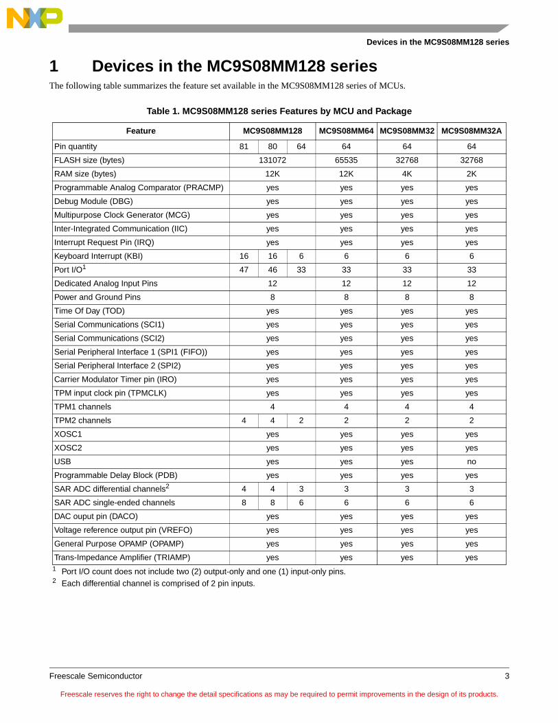
1 Devices in the MC9S08MM128 seriesThe following table summarizes the feature set available in the MC9S08MM128 series of MCUs.
Table 1. MC9S08MM128 series Features by MCU and Package
Feature MC9S08MM128 MC9S08MM64 MC9S08MM32 MC9S08MM32A
Pin quantity 81 80 64 64 64 64
FLASH size (bytes) 131072 65535 32768 32768
RAM size (bytes) 12K 12K 4K 2K
Programmable Analog Comparator (PRACMP) yes yes yes yes
Debug Module (DBG) yes yes yes yes
Multipurpose Clock Generator (MCG) yes yes yes yes
Inter-Integrated Communication (IIC) yes yes yes yes
Interrupt Request Pin (IRQ) yes yes yes yes
Keyboard Interrupt (KBI) 16 16 6 6 6 6
Port I/O1
1 Port I/O count does not include two (2) output-only and one (1) input-only pins.
47 46 33 33 33 33
Dedicated Analog Input Pins 12 12 12 12
Power and Ground Pins 8 8 8 8
Time Of Day (TOD) yes yes yes yes
Serial Communications (SCI1) yes yes yes yes
Serial Communications (SCI2) yes yes yes yes
Serial Peripheral Interface 1 (SPI1 (FIFO)) yes yes yes yes
Serial Peripheral Interface 2 (SPI2) yes yes yes yes
Carrier Modulator Timer pin (IRO) yes yes yes yes
TPM input clock pin (TPMCLK) yes yes yes yes
TPM1 channels 4 4 4 4
TPM2 channels 4 4 2 2 2 2
XOSC1 yes yes yes yes
XOSC2 yes yes yes yes
USB yes yes yes no
Programmable Delay Block (PDB) yes yes yes yes
SAR ADC differential channels2
2 Each differential channel is comprised of 2 pin inputs.
4 4 3 3 3 3
SAR ADC single-ended channels 8 8 6 6 6 6
DAC ouput pin (DACO) yes yes yes yes
Voltage reference output pin (VREFO) yes yes yes yes
General Purpose OPAMP (OPAMP) yes yes yes yes
Trans-Impedance Amplifier (TRIAMP) yes yes yes yes
Freescale reserves the right to change the detail specifications as may be required to permit improvements in the design of its products.
Devices in the MC9S08MM128 series
Freescale Semiconductor4
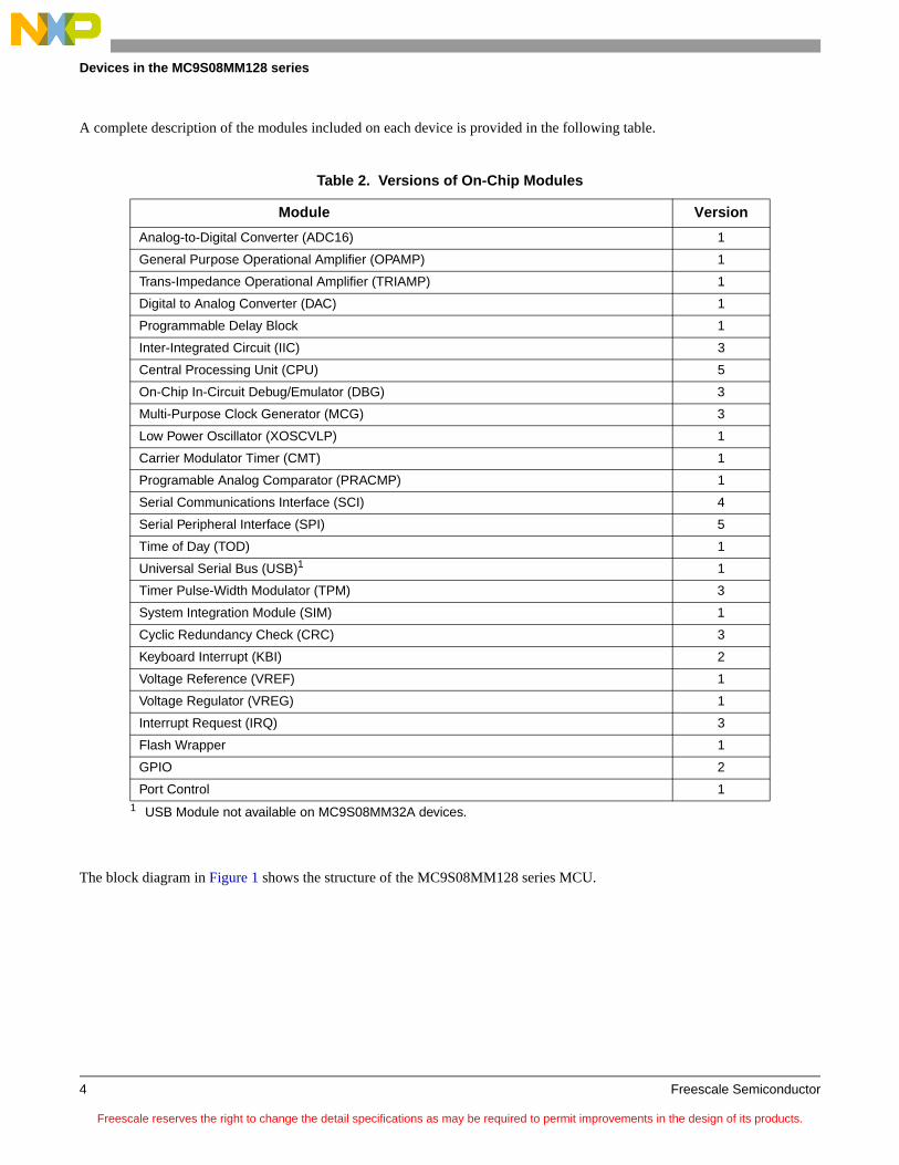
A complete description of the modules included on each device is provided in the following table.
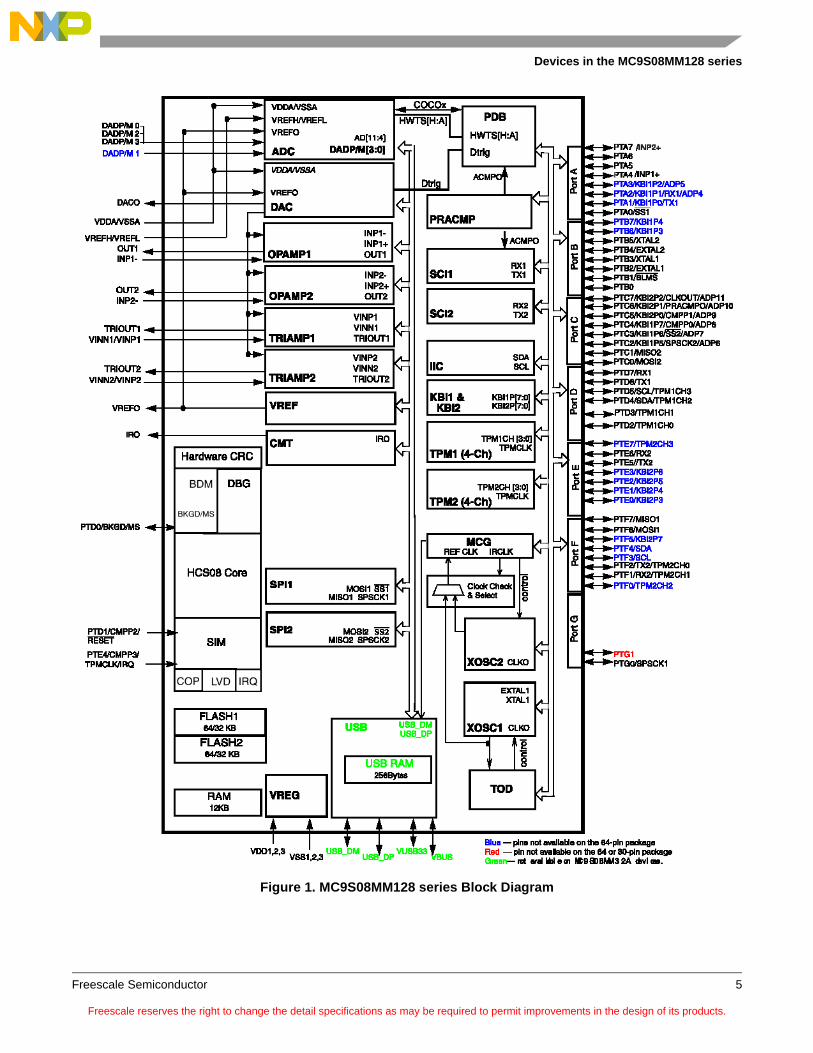
The block diagram in Figure 1 shows the structure of the MC9S08MM128 series MCU.
Table 2. Versions of On-Chip Modules
Module Version
Analog-to-Digital Converter (ADC16) 1
General Purpose Operational Amplifier (OPAMP) 1
Trans-Impedance Operational Amplifier (TRIAMP) 1
Digital to Analog Converter (DAC) 1
Programmable Delay Block 1
Inter-Integrated Circuit (IIC) 3
Central Processing Unit (CPU) 5
On-Chip In-Circuit Debug/Emulator (DBG) 3
Multi-Purpose Clock Generator (MCG) 3
Low Power Oscillator (XOSCVLP) 1
Carrier Modulator Timer (CMT) 1
Programable Analog Comparator (PRACMP) 1
Serial Communications Interface (SCI) 4
Serial Peripheral Interface (SPI) 5
Time of Day (TOD) 1
Universal Serial Bus (USB)1
1 USB Module not available on MC9S08MM32A devices.
1
Timer Pulse-Width Modulator (TPM) 3
System Integration Module (SIM) 1
Cyclic Redundancy Check (CRC) 3
Keyboard Interrupt (KBI) 2
Voltage Reference (VREF) 1
Voltage Regulator (VREG) 1
Interrupt Request (IRQ) 3
Flash Wrapper 1
GPIO 2
Port Control 1
Freescale reserves the right to change the detail specifications as may be required to permit improvements in the design of its products.
Devices in the MC9S08MM128 series
Freescale Semiconductor 5
Figure 1. MC9S08MM128 series Block Diagram
Freescale reserves the right to change the detail specifications as may be required to permit improvements in the design of its products.
Devices in the MC9S08MM128 series
Freescale Semiconductor6
1.1 Pin AssignmentsThis section shows the pin assignments for the MC9S08MM128 series devices.
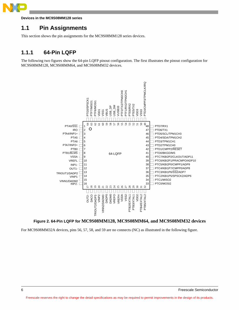
1.1.1 64-Pin LQFPThe following two figures show the 64-pin LQFP pinout configuration. The first illustrates the pinout configuration for MC9S08MM128, MC9S08MM64, and MC9S08MM32 devices.
Figure 2. 64-Pin LQFP for MC9S08MM128, MC9S08MM64, and MC9S08MM32 devices
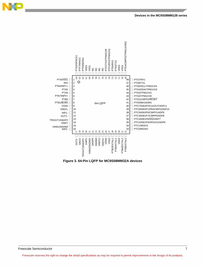
For MC9S08MM32A devices, pins 56, 57, 58, and 59 are no connects (NC) as illustrated in the following figure.
PTA0/SS1IRO
PTA5PTA6
PTB0PTB1/BLMS
12345678910111213141516
17 18 19 20 21 22 23 24 25 26 27 28 29 30 31 32
VR
EF
O
VS
S2
PT
B2/
EX
TA
L1P
TB
3/X
TA
L1V
DD
2P
TB
4/E
XT
AL2
PT
B5/
XT
AL2
48474645444342414039383736353433
PTD7/RX1PTD6/TX1PTD5/SCL/TPM1CH3PTD4/SDA/TPM1CH2PTD3/TPM1CH1PTD2/TPM1CH0PTD1/CMPP2/RESETPTD0/BKGD/MSPTC7/KBI2P2/CLKOUT/ADP11PTC6/KBI2P1/PRACMPO/ADP10PTC5/KBI2P0/CMPP1/ADP9PTC4/KBI1P7/CMPP0/ADP8PTC3/KBI1P6/SS2/ADP7PTC2/KBI1P5/SPSCK2/ADP6PTC1/MISO2PTC0/MOSI2
64 63 62 61 60 59 58 57 56 55 54 53 52 51 50 49
PT
G0/
SP
SC
K1
PT
F7/
MIS
O1
PT
F6/
MO
SI1
VD
D1
VS
S1
VB
US
US
B_D
PU
SB
_DM
VU
SB
33P
TF
2/T
X2/
TP
M2C
H0
PT
F1/
RX
2/T
PM
2CH
1P
TE
6/R
X2
PT
E5/
TX
2V
DD
3V
SS
3
64-LQFP
DA
DP
0
TR
IOU
T2/
DA
DP
3
VIN
N2/
DA
DM
3
DA
DM
0
DA
CO
VR
EF
H
VIN
P2
TRIOUT1/DADP2
VINN1/DADM2
INP1-
INP2-
OUT1-
OU
T2-
PTA4/INP1+
PTA7/INP2+
VREFL
VSSA
VINP1
VD
DA
PT
E4/
CM
PP
3/T
PM
CLK
/IRQ
Freescale reserves the right to change the detail specifications as may be required to permit improvements in the design of its products.
Devices in the MC9S08MM128 series
Freescale Semiconductor 7
Figure 3. 64-Pin LQFP for MC9S08MM32A devices
PTA0/SS1IRO
PTA5PTA6
PTB0PTB1/BLMS
12345678910111213141516
17 18 19 20 21 22 23 24 25 26 27 28 29 30 31 32
VR
EF
O
VS
S2
PT
B2/
EX
TA
L1P
TB
3/X
TA
L1V
DD
2P
TB
4/E
XT
AL2
PT
B5/
XT
AL2
48474645444342414039383736353433
PTD7/RX1PTD6/TX1PTD5/SCL/TPM1CH3PTD4/SDA/TPM1CH2PTD3/TPM1CH1PTD2/TPM1CH0PTD1/CMPP2/RESETPTD0/BKGD/MSPTC7/KBI2P2/CLKOUT/ADP11PTC6/KBI2P1/PRACMPO/ADP10PTC5/KBI2P0/CMPP1/ADP9PTC4/KBI1P7/CMPP0/ADP8PTC3/KBI1P6/SS2/ADP7PTC2/KBI1P5/SPSCK2/ADP6PTC1/MISO2PTC0/MOSI2
64 63 62 61 60 59 58 57 56 55 54 53 52 51 50 49
PT
G0/
SP
SC
K1
PT
F7/
MIS
O1
PT
F6/
MO
SI1
VD
D1
VS
S1
NC
NC
NC
NC
PT
F2/
TX
2/T
PM
2CH
0P
TF
1/R
X2/
TP
M2C
H1
PT
E6/
RX
2P
TE
5/T
X2
VD
D3
VS
S3
64-LQFP
DA
DP
0
TR
IOU
T2/
DA
DP
3
VIN
N2/
DA
DM
3
DA
DM
0
DA
CO
VR
EF
H
VIN
P2
TRIOUT1/DADP2
VINN1/DADM2
INP1-
INP2-
OUT1-
OU
T2-
PTA4/INP1+
PTA7/INP2+
VREFL
VSSA
VINP1
VD
DA
PT
E4/
CM
PP
3/T
PM
CLK
/IRQ
Freescale reserves the right to change the detail specifications as may be required to permit improvements in the design of its products.
Devices in the MC9S08MM128 series
Freescale Semiconductor8
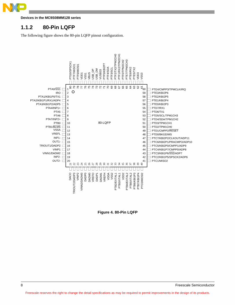
1.1.2 80-Pin LQFPThe following figure shows the 80-pin LQFP pinout configuration.
Figure 4. 80-Pin LQFP
PTA0/SS1IRO
PTA1/KBI1P0/TX1PTA2/KBI1P1/RX1/ADP4
PTA3/KBI1P2/ADP5
PTA5PTA6
PTB0PTB1/BLMS
1234567891011121314151617181920
21 22 23 24 25 26 27 28 29 30 31 32 33 34 35 36 37 38 39 40
6059585756555453525150494847464544434241
80 79 78 77 76 75 74 73 72 71 70 69 68 67 66 65 64 63 62 61
VR
EF
O
VS
S2
PT
B2/
EX
TA
L1P
TB
3/X
TA
L1V
DD
2P
TB
4/E
XT
AL2
PT
B5/
XT
AL2
PT
B6/
KB
I1P
3P
TB
7/K
BI1
P4
PT
C0/
MO
SI2
PTE3/KBI2P6PTE2/KBI2P5PTE1/KBI2P4PTE0/KBI2P3PTD7/RX1PTD6/TX1PTD5/SCL/TPM1CH3PTD4/SDA/TPM1CH2PTD3/TPM1CH1PTD2/TPM1CH0PTD1/CMPP2/RESETPTD0/BKGD/MSPTC7/KBI2P2/CLKOUT/ADP11PTC6/KBI2P1/PRACMPO/ADP10PTC5/KBI2P0/CMPP1/ADP9PTC4/KBI1P7/CMPP0/ADP8PTC3/KBI1P6/SS2/ADP7PTC2/KBI1P5/SPSCK2/ADP6PTC1/MISO2
PT
G0/
SP
SC
K1
PT
F7/
MIS
O1
PT
F6/
MO
SI1
VD
D1
VS
S1
VB
US
US
B_D
PU
SB
_DM
VU
SB
33P
TF
5/K
BI2
P7
PT
F4/
SD
AP
TF
3/S
CL
PT
F2/
TX
2/T
PM
2CH
0P
TF
1/R
X2/
TP
M2C
H1
PT
F0/
TP
M2C
H2
PT
E7/
TP
M2C
H3
PT
E6/
RX
2P
TE
5/T
X2
VD
D3
VS
S3
80-LQFP
DA
DP
0
DA
DP
1
TRIOUT1/DADP2
TR
IOU
T2/
DA
DP
3
VIN
N2/
DA
DM
3
VINN1/DADM2
DA
DM
0
DA
DM
1
INP1-
INP2-
OUT1-
OUT2-
PTA4/INP1+
PTA7/INP2+
VREFL
VSSA
VINP1
DA
CO
VR
EF
H
VIN
P2
VD
DA
PTE4/CMPP3/TPMCLK/IRQ
Freescale reserves the right to change the detail specifications as may be required to permit improvements in the design of its products.
Devices in the MC9S08MM128 series
Freescale Semiconductor 9
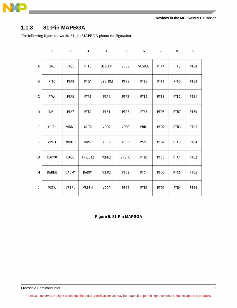
1.1.3 81-Pin MAPBGAThe following figure shows the 81-pin MAPBGA pinout configuration.
Figure 5. 81-Pin MAPBGA
1 2 3 4 5 6 7 8 9
A IRO PTG0 PTF6 USB_DP VBUS VUSB33 PTF4 PTF3 PTE4
B PTF7 PTA0 PTG1 USB_DM PTF5 PTE7 PTF1 PTF0 PTE3
C PTA4 PTA5 PTA6 PTA1 PTF2 PTE6 PTE5 PTE2 PTE1
D INP1- PTA7 PTB0 PTB1 PTA2 PTA3 PTD5 PTD7 PTE0
E OUT1 VINN1 OUT2 VDD2 VDD3 VDD1 PTD2 PTD3 PTD6
F VINP1 TRIOUT1 INP2- VSS2 VSS3 VSS1 PTB7 PTC7 PTD4
G DADP0 DACO TRIOUT2 VINN2 VREFO PTB6 PTC0 PTC1 PTC2
H DADM0 DADM1 DADP1 VINP2 PTC3 PTC4 PTD0 PTC5 PTC6
J VSSA VREFL VREFH VDDA PTB2 PTB3 PTD1 PTB4 PTB5
Freescale reserves the right to change the detail specifications as may be required to permit improvements in the design of its products.
Devices in the MC9S08MM128 series
Freescale Semiconductor10
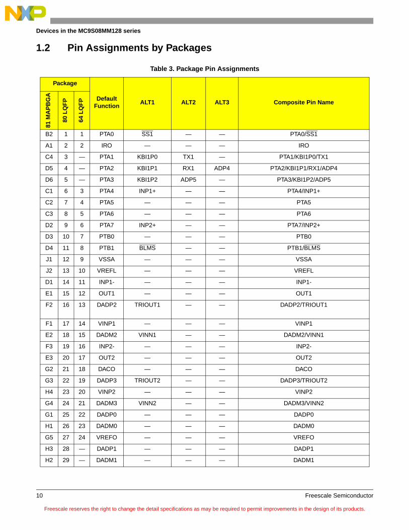
1.2 Pin Assignments by Packages
Table 3. Package Pin Assignments
Package
Default Function
ALT1 ALT2 ALT3 Composite Pin Name
81 M
AP
BG
A
80 L
QF
P
64 L
QF
P
B2 1 1 PTA0 SS1 — — PTA0/SS1
A1 2 2 IRO — — — IRO
C4 3 — PTA1 KBI1P0 TX1 — PTA1/KBI1P0/TX1
D5 4 — PTA2 KBI1P1 RX1 ADP4 PTA2/KBI1P1/RX1/ADP4
D6 5 — PTA3 KBI1P2 ADP5 — PTA3/KBI1P2/ADP5
C1 6 3 PTA4 INP1+ — — PTA4/INP1+
C2 7 4 PTA5 — — — PTA5
C3 8 5 PTA6 — — — PTA6
D2 9 6 PTA7 INP2+ — — PTA7/INP2+
D3 10 7 PTB0 — — — PTB0
D4 11 8 PTB1 BLMS — — PTB1/BLMS
J1 12 9 VSSA — — — VSSA
J2 13 10 VREFL — — — VREFL
D1 14 11 INP1- — — — INP1-
E1 15 12 OUT1 — — — OUT1
F2 16 13 DADP2 TRIOUT1 — — DADP2/TRIOUT1
F1 17 14 VINP1 — — — VINP1
E2 18 15 DADM2 VINN1 — — DADM2/VINN1
F3 19 16 INP2- — — — INP2-
E3 20 17 OUT2 — — — OUT2
G2 21 18 DACO — — — DACO
G3 22 19 DADP3 TRIOUT2 — — DADP3/TRIOUT2
H4 23 20 VINP2 — — — VINP2
G4 24 21 DADM3 VINN2 — — DADM3/VINN2
G1 25 22 DADP0 — — — DADP0
H1 26 23 DADM0 — — — DADM0
G5 27 24 VREFO — — — VREFO
H3 28 — DADP1 — — — DADP1
H2 29 — DADM1 — — — DADM1
Freescale reserves the right to change the detail specifications as may be required to permit improvements in the design of its products.
Devices in the MC9S08MM128 series
Freescale Semiconductor 11
J3 30 25 VREFH — — — VREFH
J4 31 26 VDDA — — — VDDA
F4 32 27 VSS2 — — — VSS2
J5 33 28 PTB2 EXTAL1 — — PTB2/EXTAL1
J6 34 29 PTB3 XTAL1 — — PTB3/XTAL1
E4 35 30 VDD2 — — — VDD2
J8 36 31 PTB4 EXTAL2 — — PTB4/EXTAL2
J9 37 32 PTB5 XTAL2 — — PTB5/XTAL2
G6 38 — PTB6 KBI1P3 — — PTB6/KBI1P3
F7 39 — PTB7 KBI1P4 — — PTB7/KBI1P4
G7 40 33 PTC0 MOSI2 — — PTC0/MOSI2
G8 41 34 PTC1 MISO2 — — PTC1/MISO2
G9 42 35 PTC2 KBI1P5 SPSCK2 ADP6 PTC2/KBI1P5/SPSCK2/ADP6
H5 43 36 PTC3 KBI1P6 SS2 ADP7 PTC3/KBI1P6/SS2/ADP7
H6 44 37 PTC4 KBI1P7 CMPP0 ADP8 PTC4/KBI1P7/CMPP0/ADP8
H8 45 38 PTC5 KBI2P0 CMPP1 ADP9 PTC5/KBI2P0/CMPP1/ADP9
H9 46 39 PTC6 KBI2P1 PRACMPO ADP10 PTC6/KBI2P1/PRACMPO/ADP10
F8 47 40 PTC7 KBI2P2 CLKOUT ADP11 PTC7/KBI2P2/CLKOUT/ADP11
H7 48 41 PTD0 BKGD MS — PTD0/BKGD/MS
J7 49 42 PTD1 CMPP2 RESET — PTD1/CMPP2/RESET
E7 50 43 PTD2 TPM1CH0 — — PTD2TPM1CH0
E8 51 44 PTD3 TPM1CH1 — — PTD3/TPM1CH1
F9 52 45 PTD4 SDA TPM1CH2 — PTD4/SDA/TPM1CH2
D7 53 46 PTD5 SCL TPM1CH3 — PTD5/SCL/TPM1CH3
E9 54 47 PTD6 TX1 — — PTD6/TX1
D8 55 48 PTD7 RX1 — — PTD7/RX1
D9 56 — PTE0 KBI2P3 — — PTE0/KBI2P3
C9 57 — PTE1 KBI2P4 — — PTE1/KBI2P4
C8 58 — PTE2 KBI2P5 — — PTE2/KBI2P5
B9 59 — PTE3 KBI2P6 — — PTE3/KBI2P6
A9 60 49 PTE4 CMPP3 TPMCLK IRQ PTE4/CMPP3/TPMCLK/IRQ
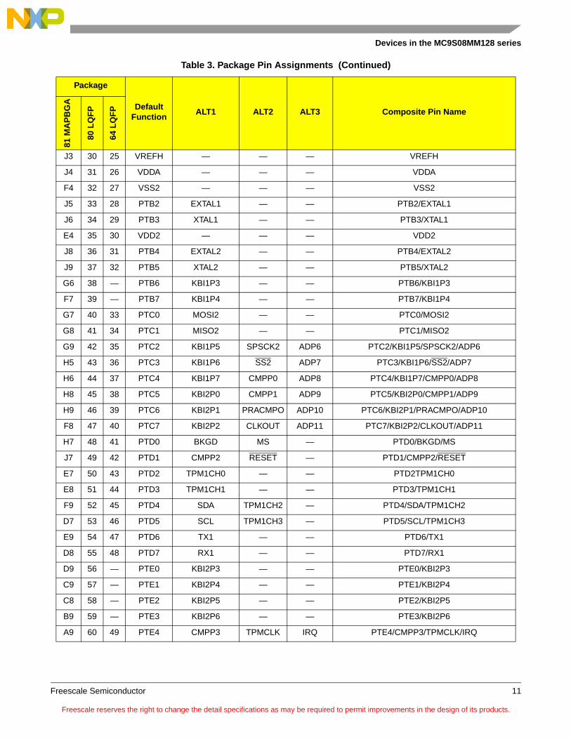
Table 3. Package Pin Assignments (Continued)
Package
Default Function
ALT1 ALT2 ALT3 Composite Pin Name
81 M
AP
BG
A
80 L
QF
P
64 L
QF
P
Freescale reserves the right to change the detail specifications as may be required to permit improvements in the design of its products.
Devices in the MC9S08MM128 series
Freescale Semiconductor12
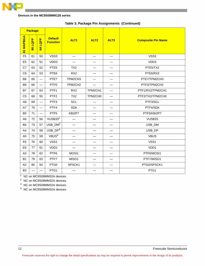
F5 61 50 VSS3 — — — VSS3
E5 62 51 VDD3 — — — VDD3
C7 63 52 PTE5 TX2 — — PTE5/TX2
C6 64 53 PTE6 RX2 — — PTE6/RX2
B6 65 — PTE7 TPM2CH3 — — PTE7/TPM2CH3
B8 66 — PTF0 TPM2CH2 — — PTF0/TPM2CH2
B7 67 54 PTF1 RX2 TPM2CH1 — PTF1/RX2/TPM2CH1
C5 68 55 PTF2 TX2 TPM2CH0 — PTF2/TX2/TPM2CH0
A8 69 — PTF3 SCL — — PTF3/SCL
A7 70 — PTF4 SDA — — PTF4/SDA
B5 71 — PTF5 KBI2P7 — — PTF5/KBI2P7
A6 72 56 VUSB331 — — — VUSB33
B4 73 57 USB_DM2 — — — USB_DM
A4 74 58 USB_DP3 — — — USB_DP
A5 75 59 VBUS4 — — — VBUS
F6 76 60 VSS1 — — — VSS1
E6 77 61 VDD1 — — — VDD1
A3 78 62 PTF6 MOSI1 — — PTF6/MOSI1
B1 79 63 PTF7 MISO1 — — PTF7/MISO1
A2 80 64 PTG0 SPSCK1 — — PTG0/SPSCK1
B3 — — PTG1 — — — PTG1
1 NC on MC9S08MM32A devices.2 NC on MC9S08MM32A devices.3 NC on MC9S08MM32A devices.4 NC on MC9S08MM32A devices.
Table 3. Package Pin Assignments (Continued)
Package
Default Function
ALT1 ALT2 ALT3 Composite Pin Name
81 M
AP
BG
A
80 L
QF
P
64 L
QF
P
Freescale reserves the right to change the detail specifications as may be required to permit improvements in the design of its products.
Electrical Characteristics
Freescale Semiconductor 13
2 Electrical Characteristics
This section contains electrical specification tables and reference timing diagrams for the MC9S08MM128/64/32/32A microcontroller, including detailed information on power considerations, DC/AC electrical characteristics, and AC timing specifications.
The electrical specifications are preliminary and are from previous designs or design simulations. These specifications may not be fully tested or guaranteed at this early stage of the product life cycle. These specifications will, however, be met for production silicon. Finalized specifications will be published after complete characterization and device qualifications have been completed.
NOTEThe parameters specified in this data sheet supersede any values found in the module specifications.
2.1 Parameter ClassificationThe electrical parameters shown in this supplement are guaranteed by various methods. To give the customer a better understanding, the following classification is used and the parameters are tagged accordingly in the tables where appropriate:
NOTEThe classification is shown in the column labeled “C” in the parameter tables where appropriate.
Table 4. Parameter Classifications
P Those parameters are guaranteed during production testing on each individual device.
CThose parameters are achieved by the design characterization by measuring a statistically relevant sample size across process variations.
TThose parameters are achieved by design characterization on a small sample size from typical devices under typical conditions unless otherwise noted. All values shown in the typical column are within this category.
D Those parameters are derived mainly from simulations.
Freescale reserves the right to change the detail specifications as may be required to permit improvements in the design of its products.
Electrical Characteristics
Freescale Semiconductor14
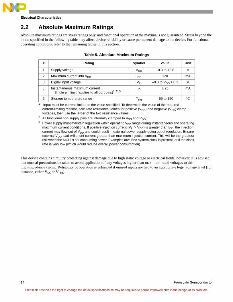
2.2 Absolute Maximum RatingsAbsolute maximum ratings are stress ratings only, and functional operation at the maxima is not guaranteed. Stress beyond the limits specified in the following table may affect device reliability or cause permanent damage to the device. For functional operating conditions, refer to the remaining tables in this section.
This device contains circuitry protecting against damage due to high static voltage or electrical fields; however, it is advised that normal precautions be taken to avoid application of any voltages higher than maximum-rated voltages to this high-impedance circuit. Reliability of operation is enhanced if unused inputs are tied to an appropriate logic voltage level (for instance, either VSS or VDD).
Table 5. Absolute Maximum Ratings
# Rating Symbol Value Unit
1 Supply voltage VDD –0.3 to +3.8 V
2 Maximum current into VDD IDD 120 mA
3 Digital input voltage VIn –0.3 to VDD + 0.3 V
4Instantaneous maximum current
Single pin limit (applies to all port pins)1, 2, 3
1 Input must be current limited to the value specified. To determine the value of the required current-limiting resistor, calculate resistance values for positive (VDD) and negative (VSS) clamp voltages, then use the larger of the two resistance values.
2 All functional non-supply pins are internally clamped to VSS and VDD.3 Power supply must maintain regulation within operating VDD range during instantaneous and operating
maximum current conditions. If positive injection current (VIn > VDD) is greater than IDD, the injection current may flow out of VDD and could result in external power supply going out of regulation. Ensure external VDD load will shunt current greater than maximum injection current. This will be the greatest risk when the MCU is not consuming power. Examples are: if no system clock is present, or if the clock rate is very low (which would reduce overall power consumption).
ID 25 mA
5 Storage temperature range Tstg –55 to 150 C
Freescale reserves the right to change the detail specifications as may be required to permit improvements in the design of its products.
Electrical Characteristics
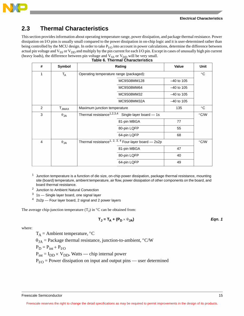
Freescale Semiconductor 15
2.3 Thermal CharacteristicsThis section provides information about operating temperature range, power dissipation, and package thermal resistance. Power dissipation on I/O pins is usually small compared to the power dissipation in on-chip logic and it is user-determined rather than being controlled by the MCU design. In order to take PI/O into account in power calculations, determine the difference between actual pin voltage and VSS or VDD and multiply by the pin current for each I/O pin. Except in cases of unusually high pin current (heavy loads), the difference between pin voltage and VSS or VDD will be very small.
The average chip-junction temperature (TJ) in C can be obtained from:
TJ = TA + (PD JA) Eqn. 1
where:
TA = Ambient temperature, CJA = Package thermal resistance, junction-to-ambient, C/W
PD = Pint PI/O
Pint = IDD VDD, Watts — chip internal power
PI/O = Power dissipation on input and output pins — user determined
Table 6. Thermal Characteristics
# Symbol Rating Value Unit
1 TA Operating temperature range (packaged): C
MC9S08MM128 –40 to 105
MC9S08MM64 –40 to 105
MC9S08MM32 –40 to 105
MC9S08MM32A –40 to 105
2 TJMAX Maximum junction temperature 135 C
3 JA Thermal resistance1,2,3,4 Single-layer board — 1s
1 Junction temperature is a function of die size, on-chip power dissipation, package thermal resistance, mounting site (board) temperature, ambient temperature, air flow, power dissipation of other components on the board, and board thermal resistance.
2 Junction to Ambient Natural Convection3 1s — Single layer board, one signal layer4 2s2p — Four layer board, 2 signal and 2 power layers
C/W
81-pin MBGA 77
80-pin LQFP 55
64-pin LQFP 68
4 JA Thermal resistance1, 2, 3, 4 Four-layer board — 2s2p C/W
81-pin MBGA 47
80-pin LQFP 40
64-pin LQFP 49
Freescale reserves the right to change the detail specifications as may be required to permit improvements in the design of its products.
Electrical Characteristics
Freescale Semiconductor16
For most applications, PI/O Pint and can be neglected. An approximate relationship between PD and TJ (if PI/O is neglected) is:
PD = K (TJ + 273C) Eqn. 2
Solving Equation 1 and Equation 2 for K gives:
K = PD (TA + 273C) + JA (PD)2 Eqn. 3
where K is a constant pertaining to the particular part. K can be determined from Equation 3 by measuring PD (at equilibrium) for a known TA. Using this value of K, the values of PD and TJ can be obtained by solving Equation 1 and Equation 2 iteratively for any value of TA.
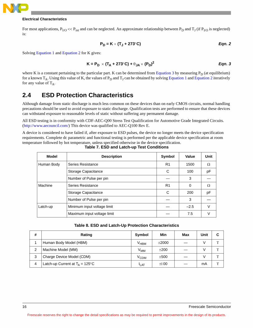
2.4 ESD Protection CharacteristicsAlthough damage from static discharge is much less common on these devices than on early CMOS circuits, normal handling precautions should be used to avoid exposure to static discharge. Qualification tests are performed to ensure that these devices can withstand exposure to reasonable levels of static without suffering any permanent damage.
All ESD testing is in conformity with CDF-AEC-Q00 Stress Test Qualification for Automotive Grade Integrated Circuits. (http://www.aecouncil.com/) This device was qualified to AEC-Q100 Rev E.
A device is considered to have failed if, after exposure to ESD pulses, the device no longer meets the device specification requirements. Complete dc parametric and functional testing is performed per the applicable device specification at room temperature followed by hot temperature, unless specified otherwise in the device specification.
Table 7. ESD and Latch-up Test Conditions
Model Description Symbol Value Unit
Human Body Series Resistance R1 1500
Storage Capacitance C 100 pF
Number of Pulse per pin — 3 —
Machine Series Resistance R1 0
Storage Capacitance C 200 pF
Number of Pulse per pin — 3 —
Latch-up Minimum input voltage limit — –2.5 V
Maximum input voltage limit — 7.5 V
Table 8. ESD and Latch-Up Protection Characteristics
# Rating Symbol Min Max Unit C
1 Human Body Model (HBM) VHBM 2000 — V T
2 Machine Model (MM) VMM 200 — V T
3 Charge Device Model (CDM) VCDM 500 — V T
4 Latch-up Current at TA = 125C ILAT 00 — mA T
Freescale reserves the right to change the detail specifications as may be required to permit improvements in the design of its products.
Electrical Characteristics
Freescale Semiconductor 17
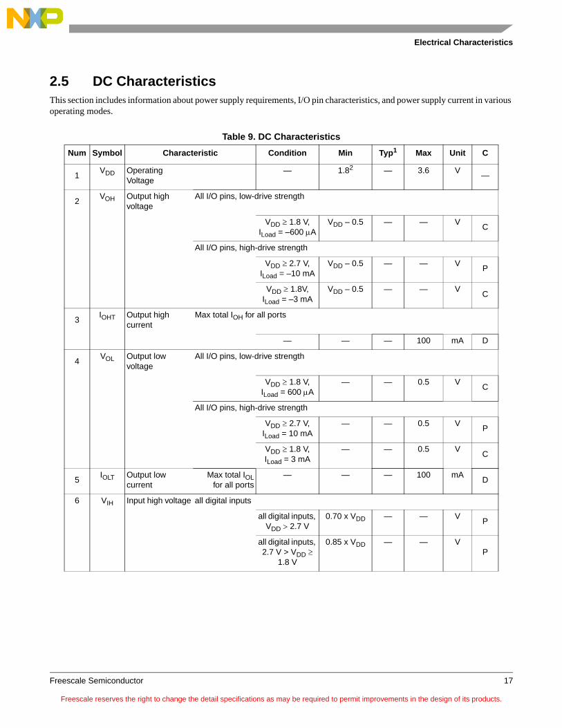
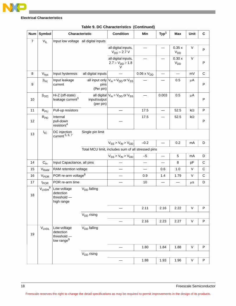
2.5 DC CharacteristicsThis section includes information about power supply requirements, I/O pin characteristics, and power supply current in various operating modes.
Table 9. DC Characteristics
Num Symbol Characteristic Condition Min Typ1 Max Unit C
1VDD Operating
Voltage— 1.82 — 3.6 V
—
2VOH Output high
voltageAll I/O pins, low-drive strength
VDD 1.8 V, ILoad = –600 A
VDD – 0.5 — — VC
All I/O pins, high-drive strength
VDD 2.7 V, ILoad = –10 mA
VDD – 0.5 — — VP
VDD 1.8V, ILoad = –3 mA
VDD – 0.5 — — VC
3IOHT Output high
currentMax total IOH for all ports
— — — 100 mA D
4VOL Output low
voltageAll I/O pins, low-drive strength
VDD 1.8 V, ILoad = 600 A
— — 0.5 VC
All I/O pins, high-drive strength
VDD 2.7 V, ILoad = 10 mA
— — 0.5 VP
VDD 1.8 V, ILoad = 3 mA
— — 0.5 VC
5IOLT Output low
currentMax total IOL
for all ports— — — 100 mA
D
6 VIH Input high voltage all digital inputs
all digital inputs, VDD 2.7 V
0.70 x VDD — — VP
all digital inputs, 2.7 V > VDD
1.8 V
0.85 x VDD — — VP
Freescale reserves the right to change the detail specifications as may be required to permit improvements in the design of its products.
Electrical Characteristics
Freescale Semiconductor18
7 VIL Input low voltage all digital inputs
all digital inputs, VDD 2.7 V
— — 0.35 x VDD
VP
all digital inputs, 2.7 VDD 1.8
V
— — 0.30 x VDD
VP
8 Vhys Input hysteresis all digital inputs — 0.06 x VDD — — mV C
9|IIn| Input leakage
currentall input only
pins(Per pin)
VIn = VDD or VSS — — 0.5 AP
10|IOZ| Hi-Z (off-state)
leakage current3 all digital
input/output(per pin)
VIn = VDD or VSS — 0.003 0.5 AP
11 RPU Pull-up resistors — 17.5 — 52.5 k P
12RPD Internal
pull-down resistors4
—17.5 — 52.5 k
P
13IIC DC injection
current 5, 6, 7Single pin limit
VSS > VIN > VDD –0.2 — 0.2 mA D
Total MCU limit, includes sum of all stressed pins
VSS > VIN > VDD –5 — 5 mA D
14 CIn Input Capacitance, all pins — — — 8 pF C
15 VRAM RAM retention voltage — — 0.6 1.0 V C
16 VPOR POR re-arm voltage8 — 0.9 1.4 1.79 V C
17 tPOR POR re-arm time — 10 — — s D
18
VLVDH9 Low-voltage
detection threshold —high range
VDD falling
— 2.11 2.16 2.22 V P
VDD rising
— 2.16 2.23 2.27 V P
19
VLVDL Low-voltage detection threshold —low range9
VDD falling
— 1.80 1.84 1.88 V P
VDD rising
— 1.88 1.93 1.96 V P
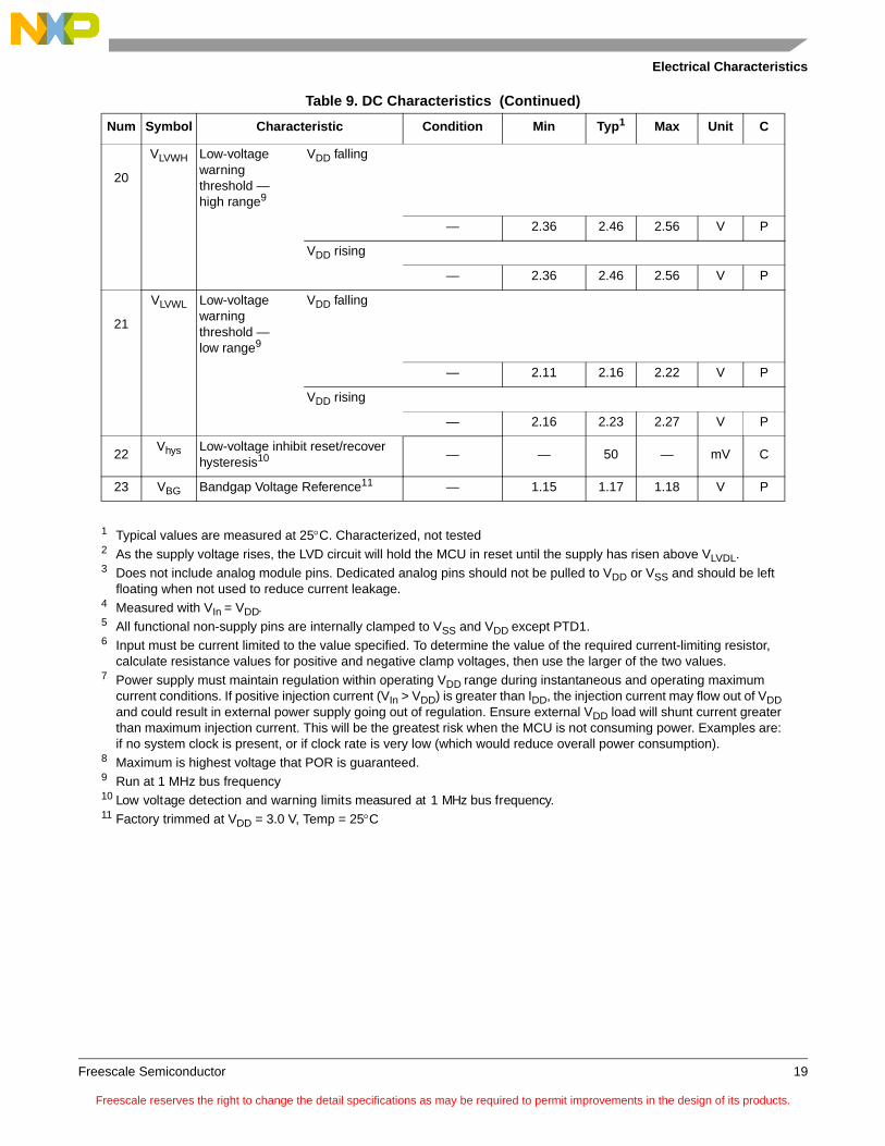
Table 9. DC Characteristics (Continued)
Num Symbol Characteristic Condition Min Typ1 Max Unit C
Freescale reserves the right to change the detail specifications as may be required to permit improvements in the design of its products.
Electrical Characteristics
Freescale Semiconductor 19
20
VLVWH Low-voltage warning threshold —high range9
VDD falling
— 2.36 2.46 2.56 V P
VDD rising
— 2.36 2.46 2.56 V P
21
VLVWL Low-voltage warning threshold —low range9
VDD falling
— 2.11 2.16 2.22 V P
VDD rising
— 2.16 2.23 2.27 V P
22Vhys Low-voltage inhibit reset/recover
hysteresis10 — — 50 — mV C
23 VBG Bandgap Voltage Reference11 — 1.15 1.17 1.18 V P
1 Typical values are measured at 25C. Characterized, not tested2 As the supply voltage rises, the LVD circuit will hold the MCU in reset until the supply has risen above VLVDL.3 Does not include analog module pins. Dedicated analog pins should not be pulled to VDD or VSS and should be left
floating when not used to reduce current leakage. 4 Measured with VIn = VDD.5 All functional non-supply pins are internally clamped to VSS and VDD except PTD1.6 Input must be current limited to the value specified. To determine the value of the required current-limiting resistor,
calculate resistance values for positive and negative clamp voltages, then use the larger of the two values.7 Power supply must maintain regulation within operating VDD range during instantaneous and operating maximum
current conditions. If positive injection current (VIn > VDD) is greater than IDD, the injection current may flow out of VDD and could result in external power supply going out of regulation. Ensure external VDD load will shunt current greater than maximum injection current. This will be the greatest risk when the MCU is not consuming power. Examples are: if no system clock is present, or if clock rate is very low (which would reduce overall power consumption).
8 Maximum is highest voltage that POR is guaranteed.9 Run at 1 MHz bus frequency10 Low voltage detection and warning limits measured at 1 MHz bus frequency.11 Factory trimmed at VDD = 3.0 V, Temp = 25C
Table 9. DC Characteristics (Continued)
Num Symbol Characteristic Condition Min Typ1 Max Unit C
Freescale reserves the right to change the detail specifications as may be required to permit improvements in the design of its products.
Electrical Characteristics
Freescale Semiconductor20
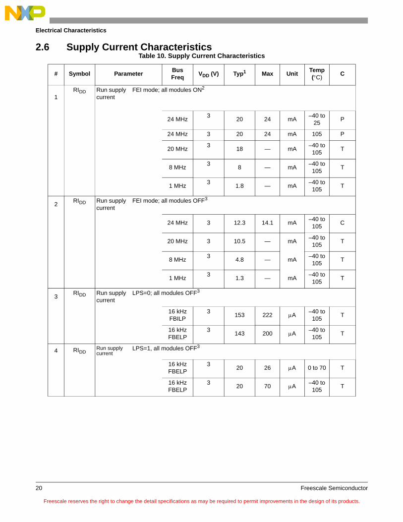
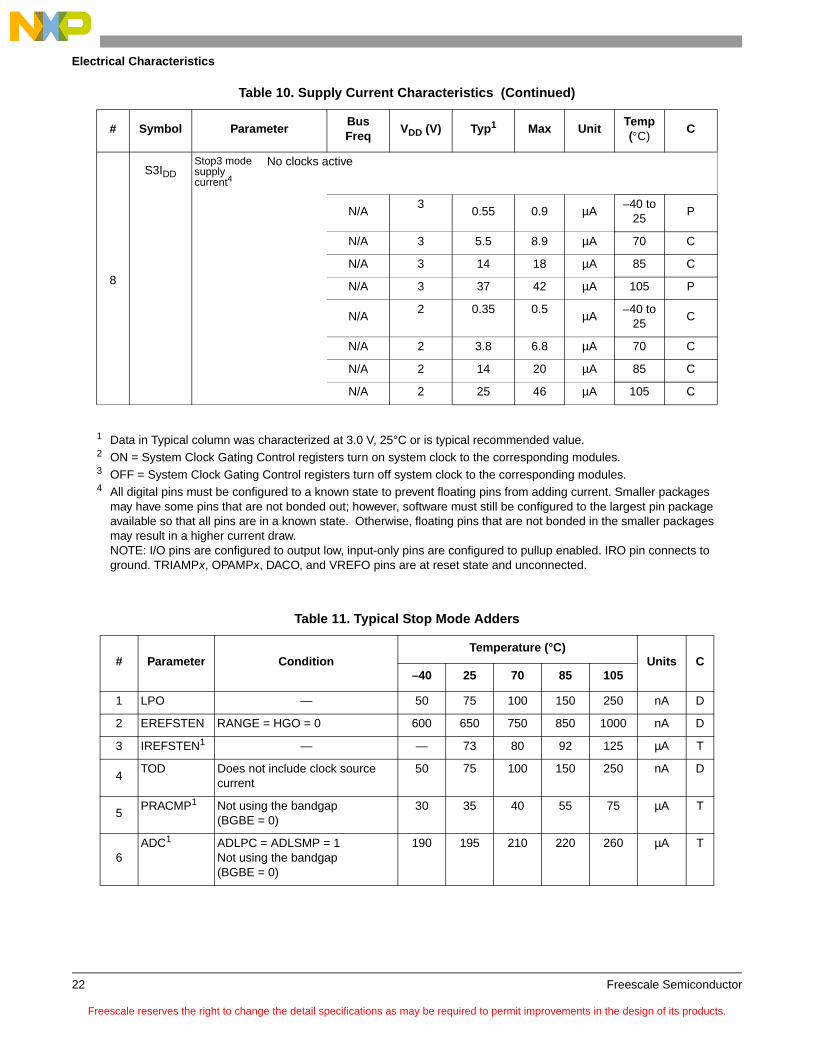
2.6 Supply Current CharacteristicsTable 10. Supply Current Characteristics
# Symbol ParameterBusFreq
VDD (V) Typ1 Max UnitTemp(C)
C
1RIDD Run supply
currentFEI mode; all modules ON2
24 MHz3
20 24 mA–40 to
25P
24 MHz 3 20 24 mA 105 P
20 MHz3
18 — mA–40 to
105T
8 MHz3
8 — mA–40 to
105T
1 MHz3
1.8 — mA–40 to
105T
2RIDD Run supply
currentFEI mode; all modules OFF3
24 MHz 3 12.3 14.1 mA–40 to
105C
20 MHz 3 10.5 — mA–40 to
105T
8 MHz3
4.8 — mA–40 to
105T
1 MHz3
1.3 — mA–40 to
105T
3RIDD Run supply
currentLPS=0; all modules OFF3
16 kHz FBILP
3153 222 A
–40 to 105
T
16 kHz FBELP
3143 200 A
–40 to 105
T
4 RIDDRun supply current
LPS=1, all modules OFF3
16 kHz FBELP
320 26 A 0 to 70 T
16 kHz FBELP
320 70 A
–40 to 105
T
Freescale reserves the right to change the detail specifications as may be required to permit improvements in the design of its products.
Electrical Characteristics
Freescale Semiconductor 21
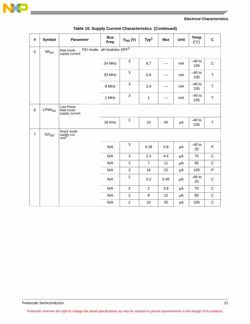
5 WIDDWait mode supply current
FEI mode, all modules OFF3
24 MHz3
6.7 — mA–40 to
105C
20 MHz3
5.6 — mA–40 to
105T
8 MHz3
2.4 — mA–40 to
105T
1 MHz3
1 — mA–40 to
105T
6 LPWIDDLow-Power Wait mode supply current
16 KHz3
10 40 µA–40 to
105T
7 S2IDDStop2 mode supply cur-rent4
N/A3
0.39 0.8 µA–40 to
25P
N/A 3 2.4 4.5 µA 70 C
N/A 3 7 11 µA 85 C
N/A 3 16 22 µA 105 P
N/A2
0.2 0.45 µA–40 to
25C
N/A 2 2 3.8 µA 70 C
N/A 2 8 12 µA 85 C
N/A 2 10 20 µA 105 C
Table 10. Supply Current Characteristics (Continued)
# Symbol ParameterBusFreq
VDD (V) Typ1 Max UnitTemp(C)
C
Freescale reserves the right to change the detail specifications as may be required to permit improvements in the design of its products.
Electrical Characteristics
Freescale Semiconductor22
8
S3IDDStop3 mode supply current4
No clocks active
N/A3
0.55 0.9 µA–40 to
25P
N/A 3 5.5 8.9 µA 70 C
N/A 3 14 18 µA 85 C
N/A 3 37 42 µA 105 P
N/A2 0.35 0.5
µA–40 to
25C
N/A 2 3.8 6.8 µA 70 C
N/A 2 14 20 µA 85 C
N/A 2 25 46 µA 105 C
1 Data in Typical column was characterized at 3.0 V, 25°C or is typical recommended value.2 ON = System Clock Gating Control registers turn on system clock to the corresponding modules.3 OFF = System Clock Gating Control registers turn off system clock to the corresponding modules.4 All digital pins must be configured to a known state to prevent floating pins from adding current. Smaller packages
may have some pins that are not bonded out; however, software must still be configured to the largest pin package available so that all pins are in a known state. Otherwise, floating pins that are not bonded in the smaller packages may result in a higher current draw. NOTE: I/O pins are configured to output low, input-only pins are configured to pullup enabled. IRO pin connects to ground. TRIAMPx, OPAMPx, DACO, and VREFO pins are at reset state and unconnected.
Table 11. Typical Stop Mode Adders
# Parameter ConditionTemperature (°C)
Units C–40 25 70 85 105
1 LPO — 50 75 100 150 250 nA D
2 EREFSTEN RANGE = HGO = 0 600 650 750 850 1000 nA D
3 IREFSTEN1 — — 73 80 92 125 µA T
4TOD Does not include clock source
current50 75 100 150 250 nA D
5PRACMP1 Not using the bandgap
(BGBE = 0)30 35 40 55 75 µA T
6ADC1 ADLPC = ADLSMP = 1
Not using the bandgap (BGBE = 0)
190 195 210 220 260 µA T
Table 10. Supply Current Characteristics (Continued)
# Symbol ParameterBusFreq
VDD (V) Typ1 Max UnitTemp(C)
C
Freescale reserves the right to change the detail specifications as may be required to permit improvements in the design of its products.

Electrical Characteristics
Freescale Semiconductor 23
2.7 PRACMP Electricals
7
DAC1 High-Power mode; no load on DACO
369 377 377 390 410 µA T
Low-Power mode 50 51 51 52 60 µA T
8OPAMP1 High-Power mode 453 538 538 540 540 µA T
Low-Power mode 56 67 67 68 70 µA T
9TRIAMP1 High-Power mode 430 432 433 438 478 µA T
Low-Power mode 52 52 52 55 60 µA T
1 Not available in stop2 mode.
Table 12. PRACMP Electrical Specifications
# Characteristic Symbol Min Typical Max Unit C
1 Supply voltage VPWR 1.8 — 3.6 V P
2 Supply current (active) (PRG enabled) IDDACT1 — — 80 A D
3 Supply current (active) (PRG disabled) IDDACT2 — — 40 A D
4Supply current (ACMP and PRG all disabled)
IDDDIS — — 2 nA D
5 Analog input voltage VAIN VSS – 0.3 — VDD V D
6 Analog input offset voltage VAIO — 5 40 mV D
7 Analog comparator hysteresis VH 3.0 — 20.0 mV D
8 Analog input leakage current IALKG — — 1 nA D
9 Analog comparator initialization delay tAINIT — — 1.0 s D
10 Programmable reference generator inputs VIn2 (VDD25) 1.8 — 2.75 V D
11Programmable reference generator setup delay
tPRGST — 1 — µs D
12Programmable reference generator step size
Vstep 0.75 1 1.25 LSB D
13Programmable reference generator voltage range
Vprgout VIn/32 — Vin V P
Table 11. Typical Stop Mode Adders (Continued)
# Parameter ConditionTemperature (°C)
Units C–40 25 70 85 105
Freescale reserves the right to change the detail specifications as may be required to permit improvements in the design of its products.
Electrical Characteristics
Freescale Semiconductor24
2.8 12-Bit DAC Electricals
Table 13. DAC 12LV Operating Requirements
# Characteristic Symbol Min Max Unit C Notes
1 Supply voltage VDDA 1.8 3.6 V P
2 Reference voltage VDACR 1.15 3.6 V C
3 Temperature TA –40 105 °C C
4Output load capacitance CL
— 100 pF C
A small load capacitance (47 pF) can improve the bandwidth performance of the DAC.
5 Output load current IL — 1 mA C
Table 14. DAC 12-Bit Operating Behaviors
# Characteristic Symbol Min Typ Max Unit C Notes
1 Resolution N 12 — 12 bit T
2 Supply current low-power mode IDDA_DACLP — 50 100 µA T
3 Supply current high-power mode IDDA_DACHP — 345 500 µA T
4
Full-scale Settling time(±1 LSB)(0x080 to 0xF7F or 0xF7F to 0x080)low-power mode
TsFSLP
— — 200 µs T
• VDDA = 3 V or 2.2 V
• VREFSEL = 1 • Temperature
= 25°C
5
Full-scale Settling time (±1 LSB)(0x080 to 0xF7F or 0xF7F to 0x080)high-power mode
TsFSHP
— — 30 µs T
• VDDA = 3 V or 2.2 V
• VREFSEL = 1 • Temperature
= 25°C
6
Code-to-code Settling time (±1 LSB)(0xBF8 to 0xC08 or 0xC08 to 0xBF8) low-power mode
TsC-CLP
— — 5 µs T
• VDDA = 3 V or 2.2 V
• VREFSEL = 1 • Temperature
= 25°C
7
Code-to-code Settling time (±1 LSB)(0xBF8 to 0xC08 or 0xC08 to 0xBF8) high-power mode (3 V at Room Temperature)
TsC-CHP
— 1 — µs T
• VDDA = 3 V or 2.2 V
• VREFSEL = 1 • Temperature
= 25°C
8
DAC output voltage range low (high-power mode, no load, DAC set to 0) (3 V at Room Temperature)
Vdacoutl
— — 100 mV T
Freescale reserves the right to change the detail specifications as may be required to permit improvements in the design of its products.
Electrical Characteristics
Freescale Semiconductor 25
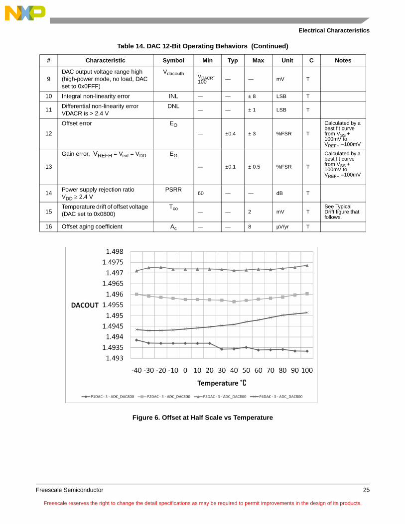
Figure 6. Offset at Half Scale vs Temperature
9DAC output voltage range high (high-power mode, no load, DAC set to 0x0FFF)
VdacouthVDACR-100 — — mV T
10 Integral non-linearity error INL — — ± 8 LSB T
11Differential non-linearity error VDACR is > 2.4 V
DNL— — ± 1 LSB T
12
Offset error EO
— ±0.4 ± 3 %FSR T
Calculated by a best fit curve from VSS + 100mV to VREFH –100mV
13
Gain error, VREFH = Vext = VDD EG
— ±0.1 ± 0.5 %FSR T
Calculated by a best fit curve from VSS + 100mV to VREFH –100mV
14Power supply rejection ratio VDD 2.4 V
PSRR60 — — dB T
15Temperature drift of offset voltage (DAC set to 0x0800)
Tco— — 2 mV T
See Typical Drift figure that follows.
16 Offset aging coefficient Ac — — 8 µV/yr T
Table 14. DAC 12-Bit Operating Behaviors (Continued)
# Characteristic Symbol Min Typ Max Unit C Notes
Freescale reserves the right to change the detail specifications as may be required to permit improvements in the design of its products.

Electrical Characteristics
Freescale Semiconductor26
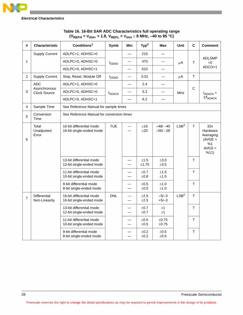
2.9 ADC Characteristics
Table 15. 16-Bit ADC Operating Conditions
# Symb Characteristic Conditions Min Typ1 Max Unit C Comment
1 VDDA Supply voltage Absolute 1.8 — 3.6 V D
2VDDA Delta to VDD
(VDD–VDDA)2–100 0 +100
mV D
3VSSA Ground voltage Delta to VSS
(VSS–VSSA)2–100 0 +100
mV D
4 VREFH Ref Voltage High 1.15 VDDA VDDA V D
5 VREFL Ref Voltage Low VSSA VSSA VSSA V D
6 VADIN Input Voltage VREFL — VREFH V D
7CADIN Input
Capacitance16-bit modes
8/10/12-bit modes— 8
4105
pF T
8 RADIN Input Resistance — 2 5 k T
9
RAS Analog Source Resistance
External to MCU
Assumes ADLSMP=0
16-bit modefADCK > 8 MHz
— — 0.5k T
4 MHz < fADCK < 8MHz
— — 1k T
fADCK < 4 MHz — — 2 k T
13/12-bit modefADCK > 8 MHz
— — 1k T
4 MHz < fADCK < 8MHz
— — 2k T
fADCK < 4 MHz — — 5 k T
11/10-bit modefADCK > 8 MHz
— — 2k T
4 MHz < fADCK < 8MHz
— — 5k T
fADCK < 4 MHz — — 10 k T
9/8-bit modefADCK > 8 MHz
— — 5k T
fADCK < 8 MHz — — 10 k T
Freescale reserves the right to change the detail specifications as may be required to permit improvements in the design of its products.
Electrical Characteristics
Freescale Semiconductor 27
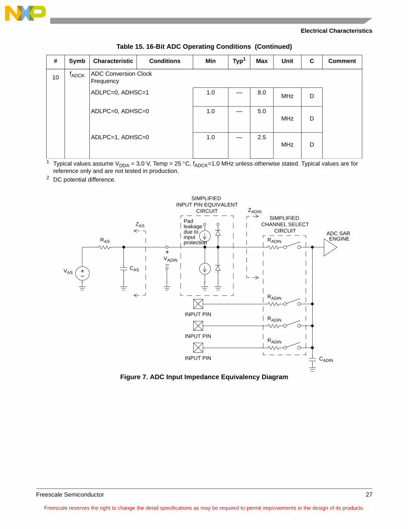
Figure 7. ADC Input Impedance Equivalency Diagram
10fADCK ADC Conversion Clock
Frequency
ADLPC=0, ADHSC=1 1.0 — 8.0MHz D
ADLPC=0, ADHSC=0 1.0 — 5.0MHz D
ADLPC=1, ADHSC=0 1.0 — 2.5MHz D
1 Typical values assume VDDA = 3.0 V, Temp = 25 C, fADCK=1.0 MHz unless otherwise stated. Typical values are for reference only and are not tested in production.
2 DC potential difference.
Table 15. 16-Bit ADC Operating Conditions (Continued)
# Symb Characteristic Conditions Min Typ1 Max Unit C Comment
+–
+
–VAS
RAS
CAS
VADIN
ZASPad leakagedue toinput protection
ZADIN
SIMPLIFIED INPUT PIN EQUIVALENT
CIRCUIT
RADIN
ADC SARENGINE
SIMPLIFIED CHANNEL SELECT
CIRCUIT
INPUT PIN
RADIN
CADIN
INPUT PIN
RADIN
INPUT PIN
RADIN
Freescale reserves the right to change the detail specifications as may be required to permit improvements in the design of its products.
Electrical Characteristics
Freescale Semiconductor28
Table 16. 16-Bit SAR ADC Characteristics full operating range
(VREFH = VDDA, > 1.8, VREFL = VSSA 8 MHz, –40 to 85 °C)
# Characteristic Conditions1 Symb Min Typ2 Max Unit C Comment
Supply Current ADLPC=1, ADHSC=0
IDDAD
— 215 —
A TADLSMP
=0ADCO=1
1 ADLPC=0, ADHSC=0 — 470 —
ADLPC=0, ADHSC=1 — 610 —
2 Supply Current Stop, Reset, Module Off IDDAD — 0.01 — A T
ADC Asynchronous Clock Source
ADLPC=1, ADHSC=0
fADACK
— 2.4 —
MHzC
tADACK = 1/fADACK
3 ADLPC=0, ADHSC=0 — 5.2 —
ADLPC=0, ADHSC=1 — 6.2 —
4 Sample Time See Reference Manual for sample times
5Conversion Time
See Reference Manual for conversion times
6
Total Unadjusted Error
16-bit differential mode16-bit single-ended mode
TUE ——
1620
48/ –4056/ –28
LSB3 T 32xHardware Averaging (AVGE =
%1AVGS =
%11)
13-bit differential mode12-bit single-ended mode
——
1.51.75
3.03.5
T
11-bit differential mode10-bit single-ended mode
——
0.70.8
1.51.5
T
9-bit differential mode8-bit single-ended mode
——
0.50.5
1.01.0
T
7Differential Non-Linearity
16-bit differential mode16-bit single-ended mode
DNL ——
2.52.5
5/–3+5/–3
LSB2 T
13-bit differential mode12-bit single-ended mode
——
0.70.7
11
T
11-bit differential mode10-bit single-ended mode
——
0.50.5
0.750.75
T
9-bit differential mode8-bit single-ended mode
——
0.20.2
0.50.5
T
Freescale reserves the right to change the detail specifications as may be required to permit improvements in the design of its products.
Electrical Characteristics
Freescale Semiconductor 29
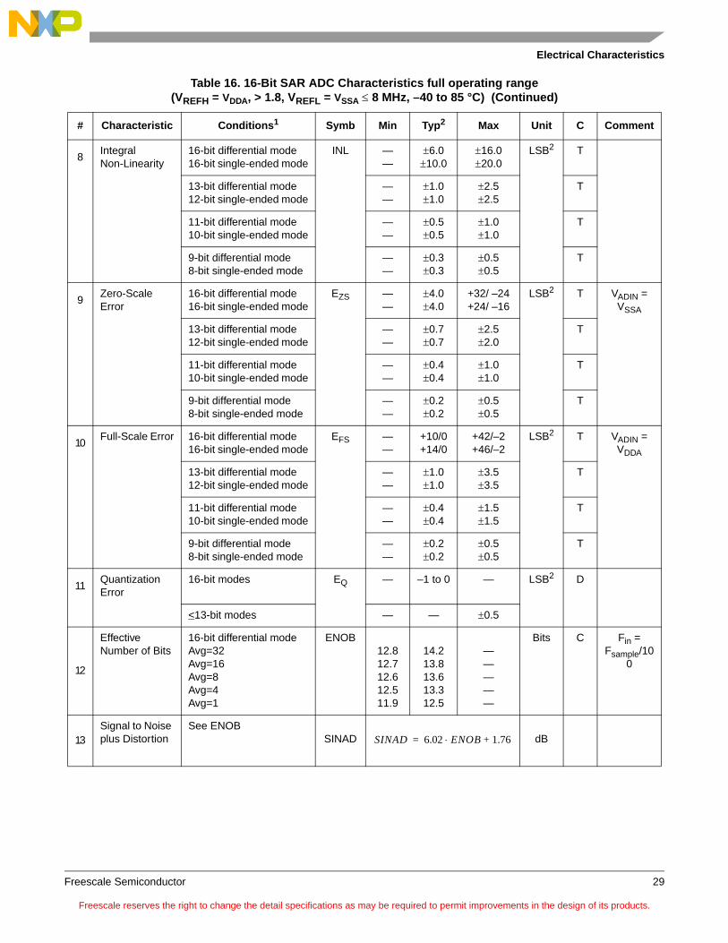
8Integral Non-Linearity
16-bit differential mode16-bit single-ended mode
INL ——
6.010.0
16.020.0
LSB2 T
13-bit differential mode12-bit single-ended mode
——
1.01.0
2.52.5
T
11-bit differential mode10-bit single-ended mode
——
0.50.5
1.01.0
T
9-bit differential mode8-bit single-ended mode
——
0.30.3
0.50.5
T
9Zero-Scale Error
16-bit differential mode16-bit single-ended mode
EZS ——
4.04.0
+32/ –24+24/ –16
LSB2 T VADIN = VSSA
13-bit differential mode12-bit single-ended mode
——
0.70.7
2.52.0
T
11-bit differential mode10-bit single-ended mode
——
0.40.4
1.01.0
T
9-bit differential mode8-bit single-ended mode
——
0.20.2
0.50.5
T
10Full-Scale Error 16-bit differential mode
16-bit single-ended modeEFS —
—+10/0+14/0
+42/–2+46/–2
LSB2 T VADIN = VDDA
13-bit differential mode12-bit single-ended mode
——
1.01.0
3.53.5
T
11-bit differential mode10-bit single-ended mode
——
0.40.4
1.51.5
T
9-bit differential mode8-bit single-ended mode
——
0.20.2
0.50.5
T
11Quantization Error
16-bit modes EQ — –1 to 0 — LSB2 D
<13-bit modes — — 0.5
12
Effective Number of Bits
16-bit differential modeAvg=32Avg=16Avg=8Avg=4Avg=1
ENOB12.812.712.612.511.9
14.213.813.613.312.5
—————
Bits C Fin = Fsample/10
0
13Signal to Noise plus Distortion
See ENOBSINAD dB
Table 16. 16-Bit SAR ADC Characteristics full operating range (VREFH = VDDA, > 1.8, VREFL = VSSA 8 MHz, –40 to 85 °C) (Continued)
# Characteristic Conditions1 Symb Min Typ2 Max Unit C Comment
SINAD 6.02 ENOB 1.76+=
Freescale reserves the right to change the detail specifications as may be required to permit improvements in the design of its products.
Electrical Characteristics
Freescale Semiconductor30
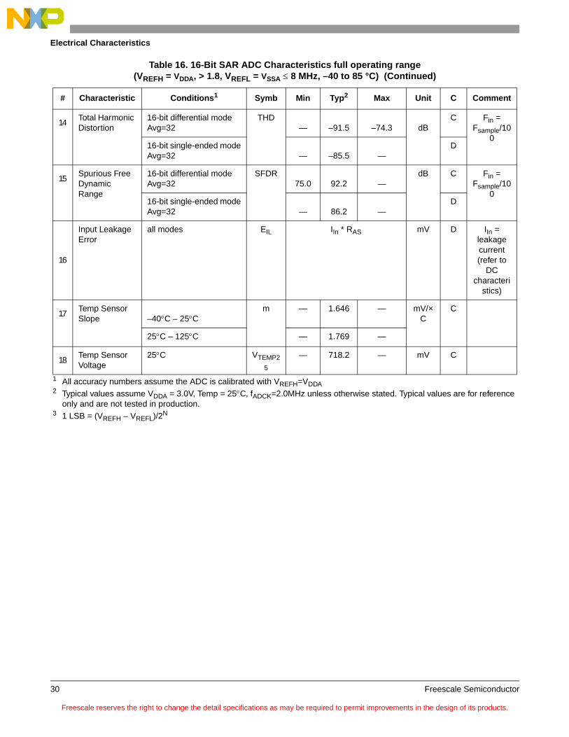
14Total Harmonic Distortion
16-bit differential modeAvg=32
THD— –91.5 –74.3 dB
C Fin = Fsample/10
016-bit single-ended modeAvg=32 — –85.5 —
D
15Spurious Free Dynamic Range
16-bit differential modeAvg=32
SFDR75.0 92.2 —
dB C Fin = Fsample/10
016-bit single-ended modeAvg=32 — 86.2 —
D
16
Input Leakage Error
all modes EIL IIn * RAS mV D IIn = leakage current (refer to
DC characteri
stics)
17Temp SensorSlope –40C – 25C
m — 1.646 — mV/×C
C
25C – 125C — 1.769 —
18Temp SensorVoltage
25C VTEMP2
5
— 718.2 — mV C
1 All accuracy numbers assume the ADC is calibrated with VREFH=VDDA2 Typical values assume VDDA = 3.0V, Temp = 25C, fADCK=2.0MHz unless otherwise stated. Typical values are for reference
only and are not tested in production.3 1 LSB = (VREFH – VREFL)/2N
Table 16. 16-Bit SAR ADC Characteristics full operating range (VREFH = VDDA, > 1.8, VREFL = VSSA 8 MHz, –40 to 85 °C) (Continued)
# Characteristic Conditions1 Symb Min Typ2 Max Unit C Comment
Freescale reserves the right to change the detail specifications as may be required to permit improvements in the design of its products.
Electrical Characteristics
Freescale Semiconductor 31
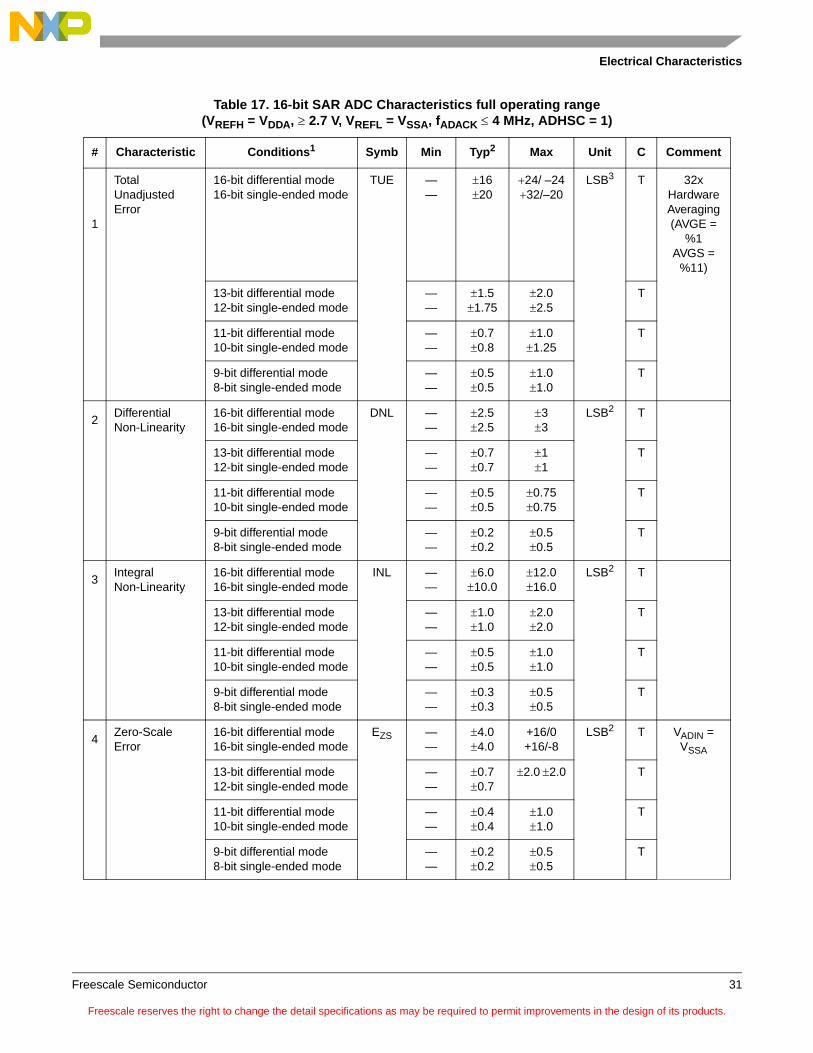
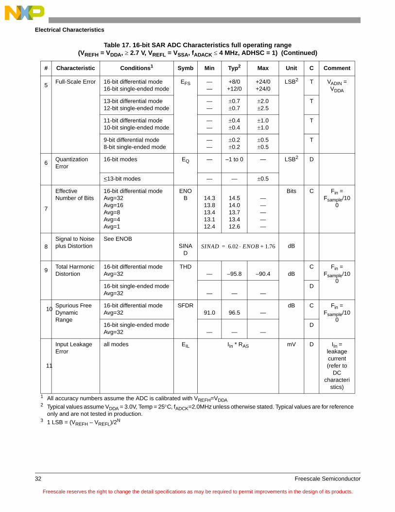
Table 17. 16-bit SAR ADC Characteristics full operating range
(VREFH = VDDA, 2.7 V, VREFL = VSSA, fADACK 4 MHz, ADHSC = 1)
# Characteristic Conditions1 Symb Min Typ2 Max Unit C Comment
1
Total Unadjusted Error
16-bit differential mode16-bit single-ended mode
TUE ——
1620
24/ –2432/–20
LSB3 T 32xHardware Averaging (AVGE =
%1AVGS =
%11)
13-bit differential mode12-bit single-ended mode
——
1.51.75
2.02.5
T
11-bit differential mode10-bit single-ended mode
——
0.70.8
1.01.25
T
9-bit differential mode8-bit single-ended mode
——
0.50.5
1.01.0
T
2Differential Non-Linearity
16-bit differential mode16-bit single-ended mode
DNL ——
2.52.5
33
LSB2 T
13-bit differential mode12-bit single-ended mode
——
0.70.7
11
T
11-bit differential mode10-bit single-ended mode
——
0.50.5
0.750.75
T
9-bit differential mode8-bit single-ended mode
——
0.20.2
0.50.5
T
3Integral Non-Linearity
16-bit differential mode16-bit single-ended mode
INL ——
6.010.0
12.016.0
LSB2 T
13-bit differential mode12-bit single-ended mode
——
1.01.0
2.02.0
T
11-bit differential mode10-bit single-ended mode
——
0.50.5
1.01.0
T
9-bit differential mode8-bit single-ended mode
——
0.30.3
0.50.5
T
4Zero-Scale Error
16-bit differential mode16-bit single-ended mode
EZS ——
4.04.0
+16/0+16/-8
LSB2 T VADIN = VSSA
13-bit differential mode12-bit single-ended mode
——
0.70.7
2.0 2.0 T
11-bit differential mode10-bit single-ended mode
——
0.40.4
1.01.0
T
9-bit differential mode8-bit single-ended mode
——
0.20.2
0.50.5
T
Freescale reserves the right to change the detail specifications as may be required to permit improvements in the design of its products.
Electrical Characteristics
Freescale Semiconductor32
5Full-Scale Error 16-bit differential mode
16-bit single-ended modeEFS —
—+8/0
+12/0+24/0+24/0
LSB2 T VADIN = VDDA
13-bit differential mode12-bit single-ended mode
——
0.70.7
2.02.5
T
11-bit differential mode10-bit single-ended mode
——
0.40.4
1.01.0
T
9-bit differential mode8-bit single-ended mode
——
0.20.2
0.50.5
T
6Quantization Error
16-bit modes EQ — –1 to 0 — LSB2 D
<13-bit modes — — 0.5
7
Effective Number of Bits
16-bit differential modeAvg=32Avg=16Avg=8Avg=4Avg=1
ENOB 14.3
13.8 13.413.112.4
14.514.013.713.412.6
—————
Bits C Fin = Fsample/10
0
8Signal to Noise plus Distortion
See ENOBSINA
DdB
9Total Harmonic Distortion
16-bit differential modeAvg=32
THD— –95.8 –90.4 dB
C Fin = Fsample/10
016-bit single-ended modeAvg=32 — — —
D
10Spurious Free Dynamic Range
16-bit differential modeAvg=32
SFDR91.0 96.5 —
dB C Fin = Fsample/10
016-bit single-ended modeAvg=32 — — —
D
11
Input Leakage Error
all modes EIL IIn * RAS mV D IIn = leakage current (refer to
DC characteri
stics)
1 All accuracy numbers assume the ADC is calibrated with VREFH=VDDA2 Typical values assume VDDA = 3.0V, Temp = 25C, fADCK=2.0MHz unless otherwise stated. Typical values are for reference
only and are not tested in production.3 1 LSB = (VREFH – VREFL)/2N
Table 17. 16-bit SAR ADC Characteristics full operating range (VREFH = VDDA, 2.7 V, VREFL = VSSA, fADACK 4 MHz, ADHSC = 1) (Continued)
# Characteristic Conditions1 Symb Min Typ2 Max Unit C Comment
SINAD 6.02 ENOB 1.76+=
Freescale reserves the right to change the detail specifications as may be required to permit improvements in the design of its products.
Electrical Characteristics
Freescale Semiconductor 33
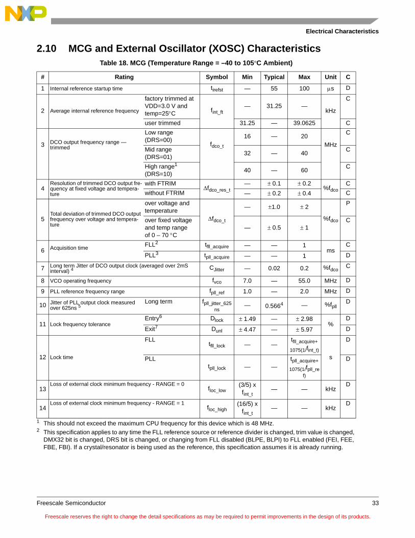
2.10 MCG and External Oscillator (XOSC) Characteristics
Table 18. MCG (Temperature Range = –40 to 105°C Ambient)
# Rating Symbol Min Typical Max Unit C
1 Internal reference startup time tirefst — 55 100 s D
2 Average internal reference frequency
factory trimmed at VDD=3.0 V and temp=25C fint_ft
— 31.25 —kHz
C
user trimmed 31.25 — 39.0625 C
3 DCO output frequency range — trimmed
Low range (DRS=00)
fdco_t
16 — 20MHz
C
Mid range (DRS=01)
32 — 40C
High range1 (DRS=10)
1 This should not exceed the maximum CPU frequency for this device which is 48 MHz.
40 — 60C
4Resolution of trimmed DCO output fre-quency at fixed voltage and tempera-ture
with FTRIMfdco_res_t
— 0.1 0.2%fdco
C
without FTRIM — 0.2 0.4 C
5Total deviation of trimmed DCO output frequency over voltage and tempera-ture
over voltage and temperature
fdco_t
— 1.0 2
%fdco
P
over fixed voltage and temp range of 0 – 70 C
— 0.5 1C
6 Acquisition time
FLL2
2 This specification applies to any time the FLL reference source or reference divider is changed, trim value is changed, DMX32 bit is changed, DRS bit is changed, or changing from FLL disabled (BLPE, BLPI) to FLL enabled (FEI, FEE, FBE, FBI). If a crystal/resonator is being used as the reference, this specification assumes it is already running.
tfll_acquire — — 1ms
C
PLL3 tpll_acquire — — 1 D
7 Long term Jitter of DCO output clock (averaged over 2mS interval) 4
CJitter — 0.02 0.2 %fdcoC
8 VCO operating frequency fvco 7.0 — 55.0 MHz D
9 PLL reference frequency range fpll_ref 1.0 — 2.0 MHz D
10 Jitter of PLL output clock measured over 625ns 5
Long term fpll_jitter_625ns
— 0.5664 — %fpllD
11 Lock frequency tolerance Entry6 Dlock 1.49 — 2.98
%D
Exit7 Dunl 4.47 — 5.97 D
12 Lock time
FLLtfll_lock — —
tfll_acquire+
1075(1/fint_t)
s
D
PLLtpll_lock — —
tpll_acquire+
1075(1/fpll_ref)
D
13Loss of external clock minimum frequency - RANGE = 0
floc_low(3/5) x fint_t
— — kHzD
14Loss of external clock minimum frequency - RANGE = 1
floc_high(16/5) x
fint_t— — kHz
D
Freescale reserves the right to change the detail specifications as may be required to permit improvements in the design of its products.

Electrical Characteristics
Freescale Semiconductor34
3 This specification applies to any time the PLL VCO divider or reference divider is changed, or changing from PLL disabled (BLPE, BLPI) to PLL enabled (PBE, PEE). If a crystal/resonator is being used as the reference, this specification assumes it is already running.
4 Jitter is the average deviation from the programmed frequency measured over the specified interval at maximum fBUS. Measurements are made with the device powered by filtered supplies and clocked by a stable external clock signal. Noise injected into the FLL circuitry via VDD and VSS and variation in crystal oscillator frequency increase the CJitter percentage for a given interval.
5 625 ns represents 5 time quanta for CAN applications, under worst-case conditions of 8 MHz CAN bus clock, 1 Mbps CAN Bus speed, and 8 time quanta per bit for bit time settings. 5 time quanta is the minimum time between a synchronization edge and the sample point of a bit using 8 time quanta per bit.
6 Below Dlock minimum, the MCG is guaranteed to enter lock. Above Dlock maximum, the MCG will not enter lock. But if the MCG is already in lock, then the MCG may stay in lock.
7 Below Dunl minimum, the MCG will not exit lock if already in lock. Above Dunl maximum, the MCG is guaranteed to exit lock.
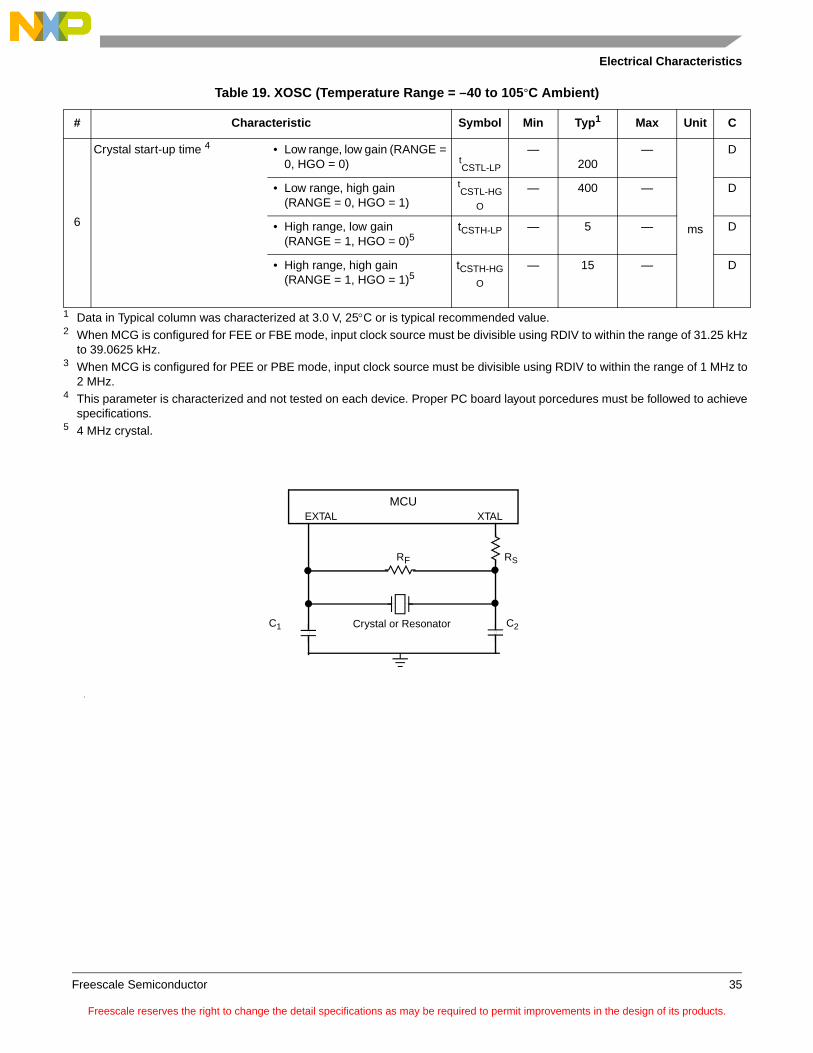
Table 19. XOSC (Temperature Range = –40 to 105°C Ambient)
# Characteristic Symbol Min Typ1 Max Unit C
1
Oscillator crystal or resonator (EREFS = 1, ERCLKEN = 1)
• Low range (RANGE = 0)flo 32 — 38.4 kHz
D
• High range (RANGE = 1), • FEE or FBE mode 2
fhi-fll 1 — 5 MHz D
• High range (RANGE = 1), • PEE or PBE mode 3
fhi-pll 1 — 16 MHz D
• High range (RANGE = 1), • High gain (HGO = 1), • BLPE mode
fhi-hgo 1 — 16 MHz D
• High range (RANGE = 1), • Low power (HGO = 0), • BLPE mode
fhi-lp 1 — 8 MHz D
2Load capacitors C1
C2
See crystal or resonator manufacturer’s recommendation.
D
3
Feedback resistor • Low range (32 kHz to 38.4 kHz)
RF —10
—
M
D
• High range (1 MHz to 16 MHz)
— — 1 — D
4Series resistor — Low range • Low Gain (HGO = 0) RS — 0 — k D
• High Gain (HGO = 1) — 100 — D
5
Series resistor — High range • Low Gain (HGO = 0) RS — 0 —
k
D
• High Gain (HGO = 1) D
8 MHz — 0 0 D
4 MHz — 0 10 D
1 MHz — 0 20 D
Freescale reserves the right to change the detail specifications as may be required to permit improvements in the design of its products.
Electrical Characteristics
Freescale Semiconductor 35
o
6
Crystal start-up time 4 • Low range, low gain (RANGE = 0, HGO = 0) t
CSTL-LP
—200
—
ms
D
• Low range, high gain (RANGE = 0, HGO = 1)
tCSTL-HG
O
— 400 — D
• High range, low gain (RANGE = 1, HGO = 0)5
tCSTH-LP — 5 — D
• High range, high gain (RANGE = 1, HGO = 1)5
tCSTH-HG
O
— 15 — D
1 Data in Typical column was characterized at 3.0 V, 25C or is typical recommended value.2 When MCG is configured for FEE or FBE mode, input clock source must be divisible using RDIV to within the range of 31.25 kHz
to 39.0625 kHz.3 When MCG is configured for PEE or PBE mode, input clock source must be divisible using RDIV to within the range of 1 MHz to
2 MHz.4 This parameter is characterized and not tested on each device. Proper PC board layout porcedures must be followed to achieve
specifications.5 4 MHz crystal.
Table 19. XOSC (Temperature Range = –40 to 105°C Ambient)
# Characteristic Symbol Min Typ1 Max Unit C
MCUEXTAL XTAL
RS
C2Crystal or Resonator
RF
C1
Freescale reserves the right to change the detail specifications as may be required to permit improvements in the design of its products.
Electrical Characteristics
Freescale Semiconductor36
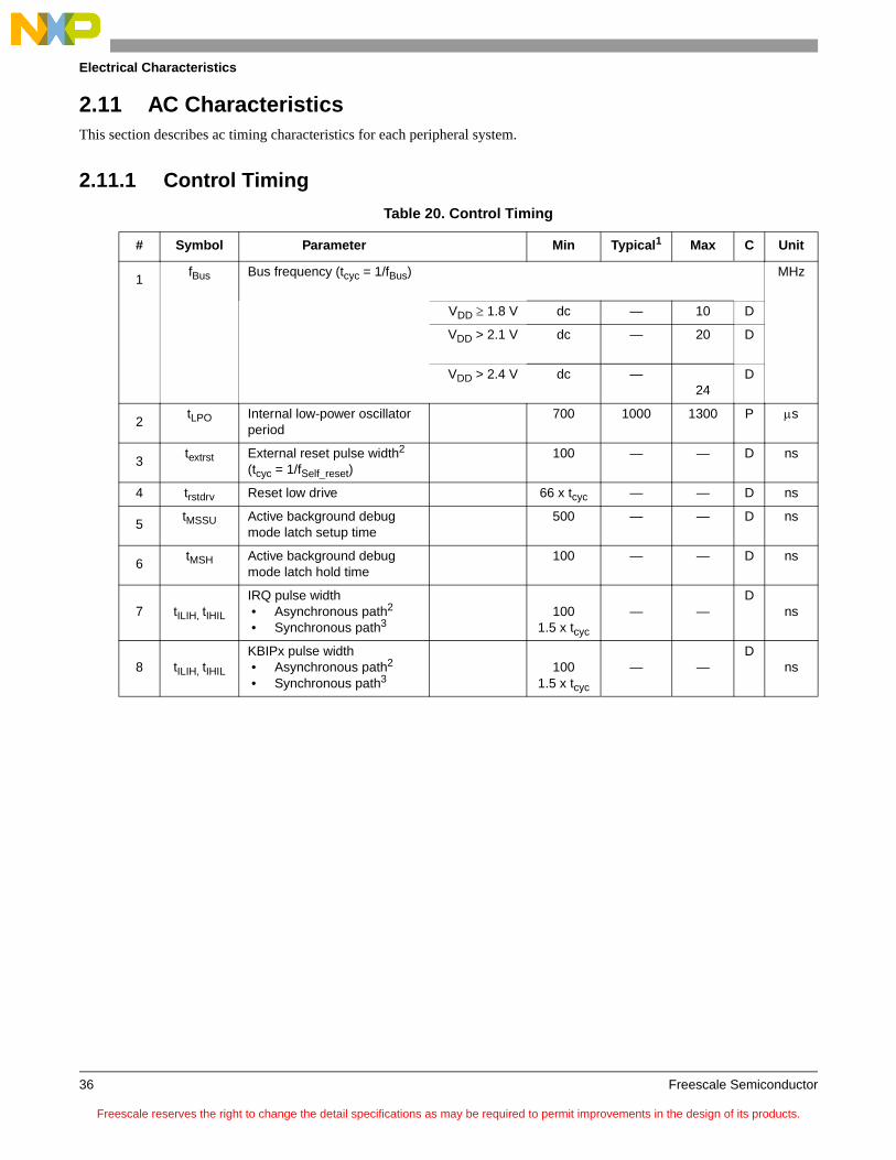
2.11 AC CharacteristicsThis section describes ac timing characteristics for each peripheral system.
2.11.1 Control Timing
Table 20. Control Timing
# Symbol Parameter Min Typical1 Max C Unit
1fBus Bus frequency (tcyc = 1/fBus) MHz
VDD 1.8 V dc — 10 D
VDD > 2.1 V dc — 20 D
VDD > 2.4 V dc —24
D
2tLPO Internal low-power oscillator
period700 1000 1300 P s
3textrst External reset pulse width2
(tcyc = 1/fSelf_reset)100 — — D ns
4 trstdrv Reset low drive 66 x tcyc — — D ns
5tMSSU Active background debug
mode latch setup time500 — — D ns
6tMSH Active background debug
mode latch hold time100 — — D ns
7 tILIH, tIHIL
IRQ pulse width • Asynchronous path2
• Synchronous path3100
1.5 x tcyc
— —D
ns
8 tILIH, tIHIL
KBIPx pulse width • Asynchronous path2
• Synchronous path3100
1.5 x tcyc
— —D
ns
Freescale reserves the right to change the detail specifications as may be required to permit improvements in the design of its products.
Electrical Characteristics
Freescale Semiconductor 37
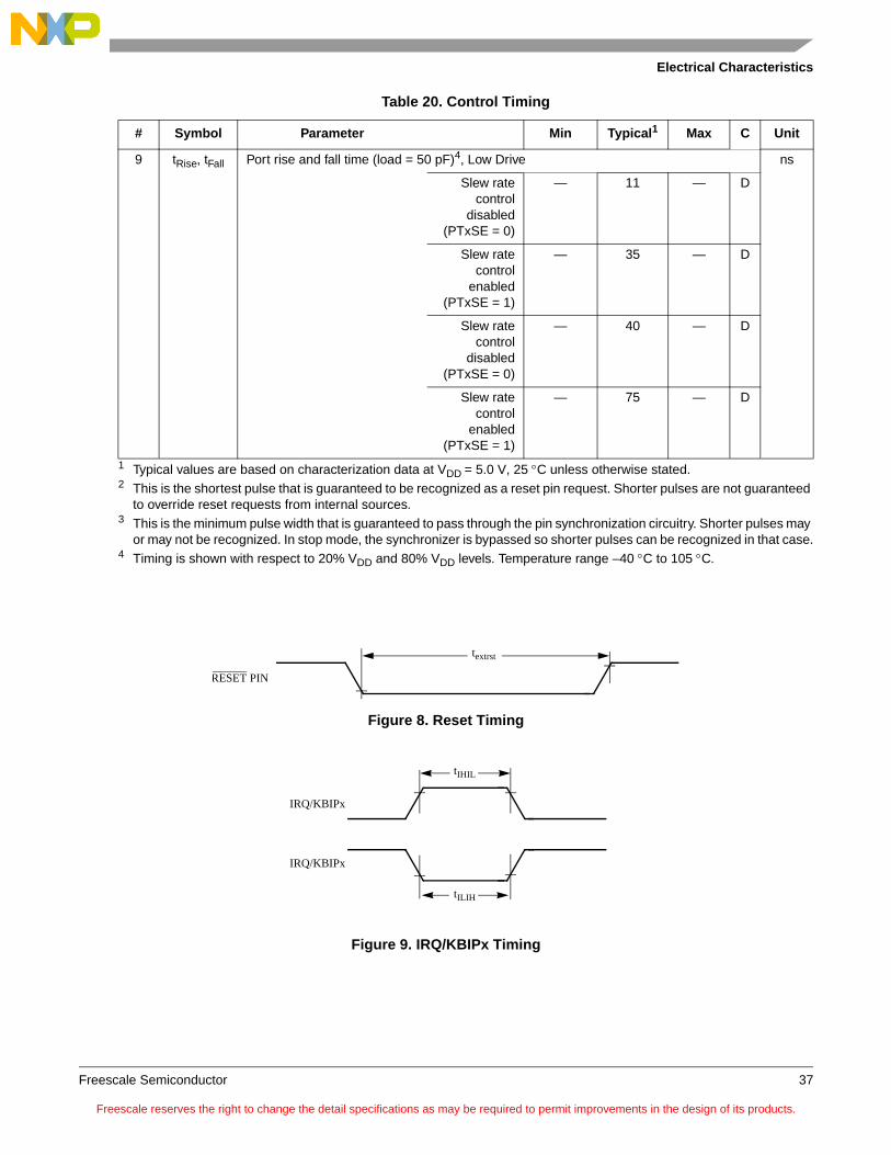
Figure 8. Reset Timing
Figure 9. IRQ/KBIPx Timing
9 tRise, tFall Port rise and fall time (load = 50 pF)4, Low Drive ns
Slew ratecontrol
disabled(PTxSE = 0)
— 11 — D
Slew ratecontrol
enabled(PTxSE = 1)
— 35 — D
Slew ratecontrol
disabled(PTxSE = 0)
— 40 — D
Slew ratecontrol
enabled(PTxSE = 1)
— 75 — D
1 Typical values are based on characterization data at VDD = 5.0 V, 25 C unless otherwise stated.2 This is the shortest pulse that is guaranteed to be recognized as a reset pin request. Shorter pulses are not guaranteed
to override reset requests from internal sources.3 This is the minimum pulse width that is guaranteed to pass through the pin synchronization circuitry. Shorter pulses may
or may not be recognized. In stop mode, the synchronizer is bypassed so shorter pulses can be recognized in that case.4 Timing is shown with respect to 20% VDD and 80% VDD levels. Temperature range –40 C to 105 C.
Table 20. Control Timing
# Symbol Parameter Min Typical1 Max C Unit
textrst
RESET PIN
tIHIL
IRQ/KBIPx
tILIH
IRQ/KBIPx
Freescale reserves the right to change the detail specifications as may be required to permit improvements in the design of its products.

Electrical Characteristics
Freescale Semiconductor38
2.11.2 TPM TimingSynchronizer circuits determine the shortest input pulses that can be recognized or the fastest clock that can be used as the optional external source to the timer counter. These synchronizers operate from the current bus rate clock.
Figure 10. Timer External Clock
Figure 11. Timer Input Capture Pulse
Table 21. TPM Input Timing
# C Function Symbol Min Max Unit
1 — External clock frequency fTPMext dc fBus/4 MHz
2 — External clock period tTPMext 4 — tcyc
3 D External clock high time tclkh 1.5 — tcyc
4 D External clock low time tclkl 1.5 — tcyc
5 D Input capture pulse width tICPW 1.5 — tcyc
tTPMext
tclkh
tclkl
TPMxCLK
tICPW
TPMxCHn
tICPW
TPMxCHn
Freescale reserves the right to change the detail specifications as may be required to permit improvements in the design of its products.
Electrical Characteristics
Freescale Semiconductor 39
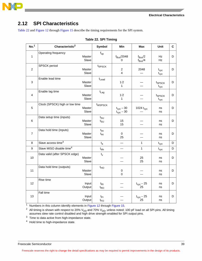
2.12 SPI CharacteristicsTable 22 and Figure 12 through Figure 15 describe the timing requirements for the SPI system.
Table 22. SPI Timing
No.1
1 Numbers in this column identify elements in Figure 12 through Figure 15.
Characteristic2
2 All timing is shown with respect to 20% VDD and 70% VDD, unless noted; 100 pF load on all SPI pins. All timing assumes slew rate control disabled and high drive strength enabled for SPI output pins.
Symbol Min Max Unit C
1Operating frequency
MasterSlave
fopfBus/2048
0fBus/2fBus/4
HzHz
D
2SPSCK period
MasterSlave
tSPSCK24
2048—
tcyctcyc
D
3Enable lead time
MasterSlave
tLead121
——
tSPSCKtcyc
D
4Enable lag time
MasterSlave
tLag121
——
tSPSCKtcyc
D
5Clock (SPSCK) high or low time
MasterSlave
tWSPSCKtcyc –30tcyc – 30
1024 tcyc—
nsns
D
6Data setup time (inputs)
MasterSlave
tSUtSU 15
15——
nsns
D
7Data hold time (inputs)
MasterSlave
tHItHI 0
25——
nsns
D
8 Slave access time3
3 Time to data active from high-impedance state.
ta — 1 tcyc D
9 Slave MISO disable time4
4 Hold time to high-impedance state.
tdis — 1 tcyc D
10Data valid (after SPSCK edge)
MasterSlave
tv——
2525
nsns
D
11Data hold time (outputs)
MasterSlave
tHO00
——
nsns
D
12Rise time
InputOutput
tRItRO
——
tcyc – 2525
nsns
D
13Fall time
InputOutput
tFItFO
——
tcyc – 2525
nsns
D
Freescale reserves the right to change the detail specifications as may be required to permit improvements in the design of its products.

Electrical Characteristics
Freescale Semiconductor40
Figure 12. SPI Master Timing (CPHA = 0)
Figure 13. SPI Master Timing (CPHA = 1)
SCK
(OUTPUT)
SCK
(OUTPUT)
MISO(INPUT)
MOSI(OUTPUT)
SS1
(OUTPUT)
MSB IN2
BIT 6 . . . 1
LSB IN
MSB OUT2 LSB OUT
BIT 6 . . . 1
(CPOL = 0)
(CPOL = 1)
NOTES:
2. LSBF = 0. For LSBF = 1, bit order is LSB, bit 1, ..., bit 6, MSB.1. SS output mode (MODFEN = 1, SSOE = 1).
22 3
5
6 7
11 12
5
11
4
4
SCK
(OUTPUT)
SCK
(OUTPUT)
MISO(INPUT)
MOSI(OUTPUT)
MSB IN(2)
BIT 6 . . . 1
LSB IN
MSB OUT(2) LSB OUT
BIT 6 . . . 1
(CPOL = 0)
(CPOL = 1)
SS(1)
(OUTPUT)
1. SS output mode (MODFEN = 1, SSOE = 1).2. LSBF = 0. For LSBF = 1, bit order is LSB, bit 1, ..., bit 6, MSB.
NOTES:
2
2
3
4
5
6 7
11 12
54
Freescale reserves the right to change the detail specifications as may be required to permit improvements in the design of its products.
Electrical Characteristics
Freescale Semiconductor 41
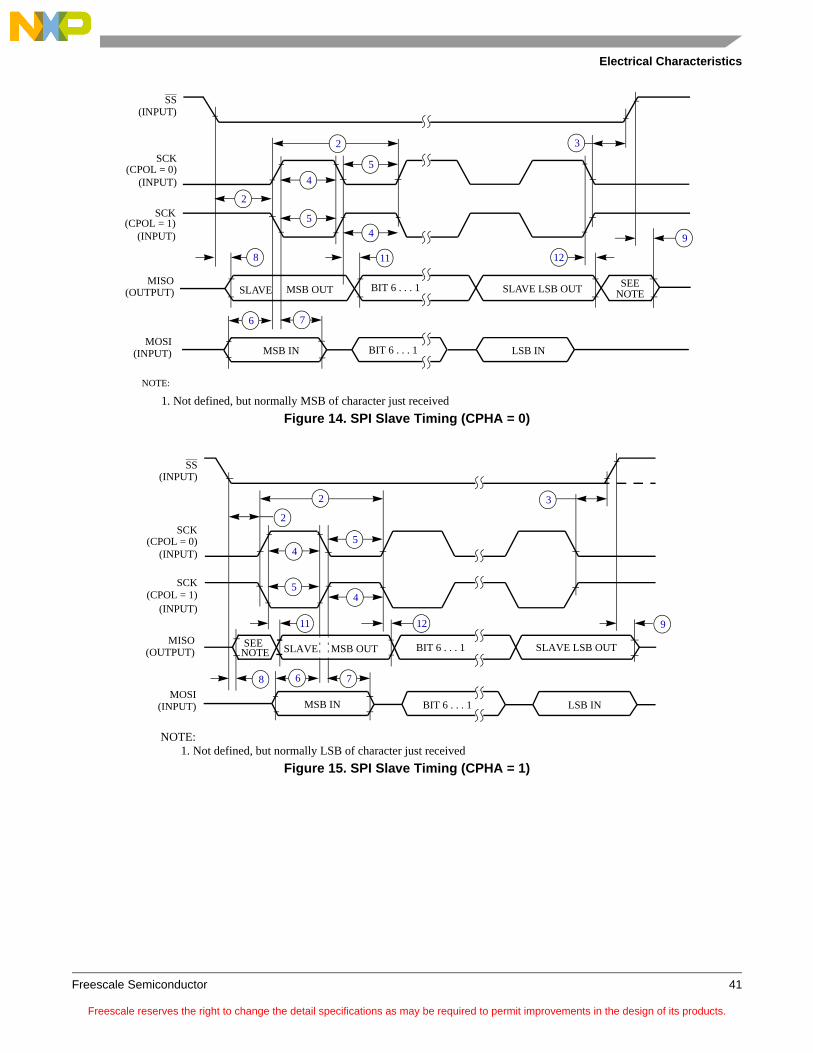
Figure 14. SPI Slave Timing (CPHA = 0)
Figure 15. SPI Slave Timing (CPHA = 1)
SCK
(INPUT)
SCK
(INPUT)
MOSI(INPUT)
MISO(OUTPUT)
SS(INPUT)
MSB IN
BIT 6 . . . 1
LSB IN
MSB OUT SLAVE LSB OUT
BIT 6 . . . 1
(CPOL = 0)
(CPOL = 1)
NOTE:
SLAVESEE
NOTE
1. Not defined, but normally MSB of character just received
2
2
3
4
6 7
8
9
11 12
5
54
SCK
(INPUT)
SCK
(INPUT)
MOSI(INPUT)
MISO(OUTPUT)
MSB IN
BIT 6 . . . 1
LSB IN
MSB OUT SLAVE LSB OUT
BIT 6 . . . 1
SEE
(CPOL = 0)
(CPOL = 1)
SS(INPUT)
NOTE:
SLAVE NOTE
1. Not defined, but normally LSB of character just received
2
2
3
4
6 78
911 12
45
5
Freescale reserves the right to change the detail specifications as may be required to permit improvements in the design of its products.
Electrical Characteristics
Freescale Semiconductor42
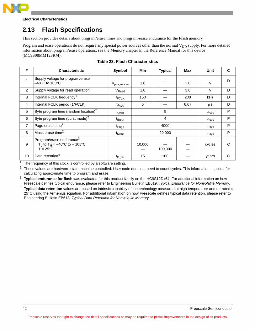
2.13 Flash SpecificationsThis section provides details about program/erase times and program-erase endurance for the Flash memory.
Program and erase operations do not require any special power sources other than the normal VDD supply. For more detailed information about program/erase operations, see the Memory chapter in the Reference Manual for this device (MC9S08MM128RM).
Table 23. Flash Characteristics
# Characteristic Symbol Min Typical Max Unit C
1Supply voltage for program/erase–40C to 105C Vprog/erase 1.8
—3.6 V
D
2 Supply voltage for read operation VRead 1.8 — 3.6 V D
3 Internal FCLK frequency1
1 The frequency of this clock is controlled by a software setting.
fFCLK 150 — 200 kHz D
4 Internal FCLK period (1/FCLK) tFcyc 5 — 6.67 s D
5 Byte program time (random location)2 tprog 9 tFcyc P
6 Byte program time (burst mode)2 tBurst 4 tFcyc P
7 Page erase time2
2 These values are hardware state machine controlled. User code does not need to count cycles. This information supplied for calculating approximate time to program and erase.
tPage 4000 tFcyc P
8 Mass erase time2 tMass 20,000 tFcyc P
9Program/erase endurance3
TL to TH = –40C to + 105CT = 25C
3 Typical endurance for flash was evaluated for this product family on the HC9S12Dx64. For additional information on how Freescale defines typical endurance, please refer to Engineering Bulletin EB619, Typical Endurance for Nonvolatile Memory.
10,000—
—100,000
——
cycles C
10 Data retention4
4 Typical data retention values are based on intrinsic capability of the technology measured at high temperature and de-rated to 25C using the Arrhenius equation. For additional information on how Freescale defines typical data retention, please refer to Engineering Bulletin EB618, Typical Data Retention for Nonvolatile Memory.
tD_ret 15 100 — years C
Freescale reserves the right to change the detail specifications as may be required to permit improvements in the design of its products.
Electrical Characteristics
Freescale Semiconductor 43
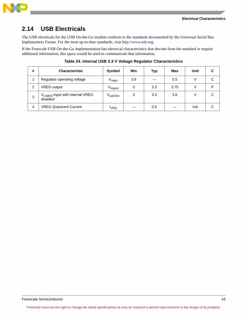
2.14 USB ElectricalsThe USB electricals for the USB On-the-Go module conform to the standards documented by the Universal Serial Bus Implementers Forum. For the most up-to-date standards, visit http://www.usb.org.
If the Freescale USB On-the-Go implementation has electrical characteristics that deviate from the standard or require additional information, this space would be used to communicate that information.
Table 24. Internal USB 3.3 V Voltage Regulator Characteristics
# Characteristic Symbol Min Typ Max Unit C
1 Regulator operating voltage Vregin 3.9 — 5.5 V C
2 VREG output Vregout 3 3.3 3.75 V P
3VUSB33 input with internal VREG disabled
Vusb33in 3 3.3 3.6 V C
4 VREG Quiescent Current IVRQ — 0.5 — mA C
Freescale reserves the right to change the detail specifications as may be required to permit improvements in the design of its products.
Electrical Characteristics
Freescale Semiconductor44
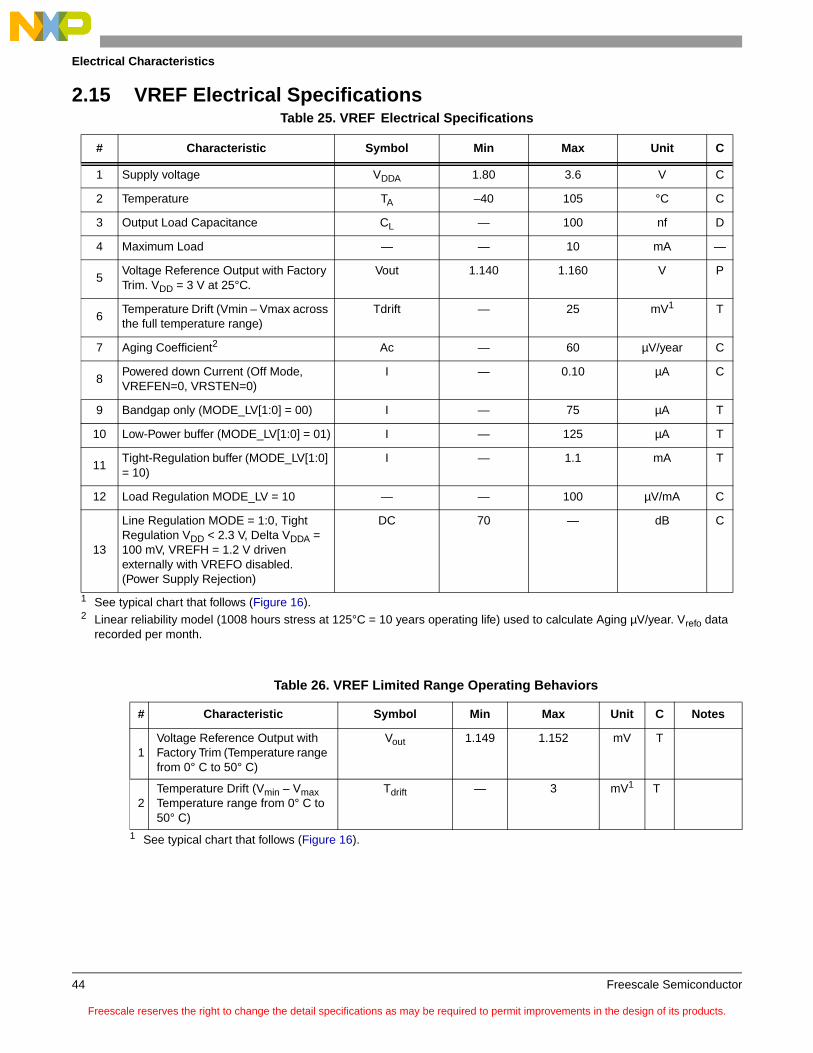
2.15 VREF Electrical Specifications
Table 25. VREF Electrical Specifications
# Characteristic Symbol Min Max Unit C
1 Supply voltage VDDA 1.80 3.6 V C
2 Temperature TA –40 105 °C C
3 Output Load Capacitance CL — 100 nf D
4 Maximum Load — — 10 mA —
5Voltage Reference Output with Factory Trim. VDD = 3 V at 25°C.
Vout 1.140 1.160 V P
6Temperature Drift (Vmin – Vmax across the full temperature range)
Tdrift — 25 mV1
1 See typical chart that follows (Figure 16).
T
7 Aging Coefficient2
2 Linear reliability model (1008 hours stress at 125°C = 10 years operating life) used to calculate Aging µV/year. Vrefo data recorded per month.
Ac — 60 µV/year C
8Powered down Current (Off Mode, VREFEN=0, VRSTEN=0)
I — 0.10 µA C
9 Bandgap only (MODE_LV[1:0] = 00) I — 75 µA T
10 Low-Power buffer (MODE_LV[1:0] = 01) I — 125 µA T
11Tight-Regulation buffer (MODE_LV[1:0] = 10)
I — 1.1 mA T
12 Load Regulation MODE_LV = 10 — — 100 µV/mA C
13
Line Regulation MODE = 1:0, Tight Regulation VDD < 2.3 V, Delta VDDA = 100 mV, VREFH = 1.2 V driven externally with VREFO disabled. (Power Supply Rejection)
DC 70 — dB C
Table 26. VREF Limited Range Operating Behaviors
# Characteristic Symbol Min Max Unit C Notes
1Voltage Reference Output with Factory Trim (Temperature range from 0° C to 50° C)
Vout 1.149 1.152 mV T
2Temperature Drift (Vmin – Vmax Temperature range from 0° C to 50° C)
Tdrift — 3 mV1
1 See typical chart that follows (Figure 16).
T
Freescale reserves the right to change the detail specifications as may be required to permit improvements in the design of its products.
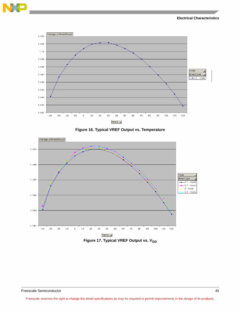
Electrical Characteristics
Freescale Semiconductor 45
Figure 16. Typical VREF Output vs. Temperature
Figure 17. Typical VREF Output vs. VDD
Freescale reserves the right to change the detail specifications as may be required to permit improvements in the design of its products.
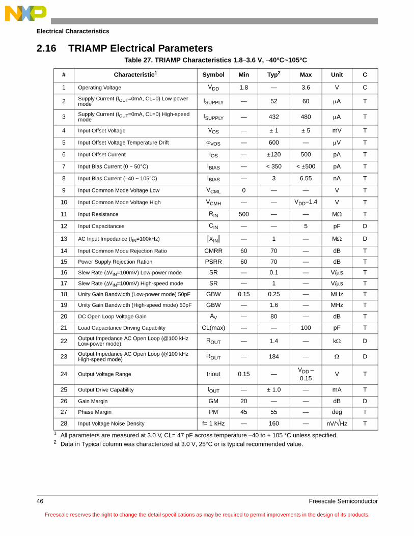
Electrical Characteristics
Freescale Semiconductor46
2.16 TRIAMP Electrical ParametersTable 27. TRIAMP Characteristics 1.8–3.6 V, –40°C~105°C
# Characteristic1
1 All parameters are measured at 3.0 V, CL= 47 pF across temperature –40 to + 105 °C unless specified.
Symbol Min Typ2
2 Data in Typical column was characterized at 3.0 V, 25°C or is typical recommended value.
Max Unit C
1 Operating Voltage VDD 1.8 — 3.6 V C
2 Supply Current (IOUT=0mA, CL=0) Low-power mode
ISUPPLY — 52 60 A T
3 Supply Current (IOUT=0mA, CL=0) High-speed mode
ISUPPLY — 432 480 A T
4 Input Offset Voltage VOS — ± 1 ± 5 mV T
5 Input Offset Voltage Temperature Drift VOS — 600 — V T
6 Input Offset Current IOS — ±120 500 pA T
7 Input Bias Current (0 ~ 50°C) IBIAS — < 350 < ±500 pA T
8 Input Bias Current (–40 ~ 105°C) IBIAS — 3 6.55 nA T
9 Input Common Mode Voltage Low VCML 0 — — V T
10 Input Common Mode Voltage High VCMH — — VDD–1.4 V T
11 Input Resistance RIN 500 — — M T
12 Input Capacitances CIN — — 5 pF D
13 AC Input Impedance (fIN=100kHz) |XIN| — 1 — M D
14 Input Common Mode Rejection Ratio CMRR 60 70 — dB T
15 Power Supply Rejection Ration PSRR 60 70 — dB T
16 Slew Rate (VIN=100mV) Low-power mode SR — 0.1 — V/s T
17 Slew Rate (VIN=100mV) High-speed mode SR — 1 — V/s T
18 Unity Gain Bandwidth (Low-power mode) 50pF GBW 0.15 0.25 — MHz T
19 Unity Gain Bandwidth (High-speed mode) 50pF GBW — 1.6 — MHz T
20 DC Open Loop Voltage Gain AV — 80 — dB T
21 Load Capacitance Driving Capability CL(max) — — 100 pF T
22 Output Impedance AC Open Loop (@100 kHz Low-power mode)
ROUT — 1.4 — k D
23 Output Impedance AC Open Loop (@100 kHz High-speed mode)
ROUT — 184 — D
24 Output Voltage Range triout 0.15 —VDD – 0.15
V T
25 Output Drive Capability IOUT — ± 1.0 — mA T
26 Gain Margin GM 20 — — dB D
27 Phase Margin PM 45 55 — deg T
28 Input Voltage Noise Density f= 1 kHz — 160 — nV/Hz T
Freescale reserves the right to change the detail specifications as may be required to permit improvements in the design of its products.
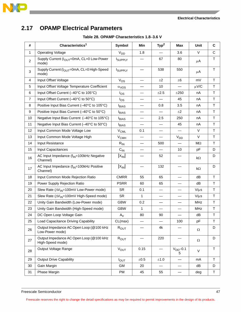
Electrical Characteristics
Freescale Semiconductor 47
2.17 OPAMP Electrical ParametersTable 28. OPAMP Characteristics 1.8–3.6 V
# Characteristics1 Symbol Min Typ2 Max Unit C
1 Operating Voltage VDD 1.8 — 3.6 V C
2Supply Current (IOUT=0mA, CL=0 Low-Power mode)
ISUPPLY — 67 80A
T
3Supply Current (IOUT=0mA, CL=0 High-Speed mode)
ISUPPLY — 538 550A
T
4 Input Offset Voltage VOS — 2 6 mV T
5 Input Offset Voltage Temperature Coefficient VOS — 10 — V/C T
6 Input Offset Current (–40°C to 105°C) IOS — 2.5 250 nA T
7 Input Offset Current (–40°C to 50°C) IOS — — 45 nA T
8 Positive Input Bias Current (–40°C to 105°C) IBIAS — 0.8 3.5 nA T
9 Positive Input Bias Current (–40°C to 50°C) IBIAS — — 2 nA T
10 Negative Input Bias Current (–40°C to 105°C) IBIAS — 2.5 250 nA T
11 Negative Input Bias Current (–40°C to 50°C) IBIAS — — 45 nA T
12 Input Common Mode Voltage Low VCML 0.1 — — V T
13 Input Common Mode Voltage High VCMH — — VDD V T
14 Input Resistance RIN — 500 — M T
15 Input Capacitances CIN — — 10 pF D
16AC Input Impedance (fIN=100kHz Negative Channel)
|XIN| — 52 —k
D
17AC Input Impedance (fIN=100kHz Positive Channel)
|XIN| — 132 —k
D
18 Input Common Mode Rejection Ratio CMRR 55 65 — dB T
19 Power Supply Rejection Ratio PSRR 60 65 — dB T
20 Slew Rate (VIN=100mV Low-Power mode) SR 0.1 — — V/s T
21 Slew Rate (VIN=100mV High-Speed mode) SR 1 — — V/s T
22 Unity Gain Bandwidth (Low-Power mode) GBW 0.2 — — MHz T
23 Unity Gain Bandwidth (High-Speed mode) GBW 1 — — MHz T
24 DC Open Loop Voltage Gain AV 80 90 — dB T
25 Load Capacitance Driving Capability CL(max) — — 100 pF T
26Output Impedance AC Open Loop (@100 kHz Low-Power mode)
ROUT — 4k — D
27Output Impedance AC Open Loop (@100 kHz High-Speed mode)
ROUT — 220 — D
28Output Voltage Range VOUT 0.15 — VDD–0.1
5V
T
29 Output Drive Capability IOUT 0.5 1.0 — mA T
30 Gain Margin GM 20 — — dB D
31 Phase Margin PM 45 55 — deg T
Freescale reserves the right to change the detail specifications as may be required to permit improvements in the design of its products.
Ordering Information
Freescale Semiconductor48
3 Ordering InformationThis appendix contains ordering information for the device numbering system. MC9S08MM128 and MC9S08MM64 devices.
3.1 Device Numbering SystemExample of the device numbering system:
32GPAMP startup time (Low-Power mode) (Tolerance < 1%, Vin = 0.5 Vp–p, CL = 25 pF, RL = 100k)
Tstartup — 4 —uS
T
33GPAMP startup time (Low-Power mode) (Tolerance < 1%, Vin = 0.5 Vp–p, CL = 25 pF, RL = 100k)
Tstartup — 1 —uS
T
34 Input Voltage Noise Density f=1 kHz — 250 — nV/Hz T
1 All parameters are measured at 3.3 V, CL =4 7 pF across temperature –40 to + 105°C unless specified.2 Data in Typical column was characterized at 3.0 V, 25°C or is typical recommended value.
Table 29. Device Numbering System
Device Number1
1 See Table 2 for a complete description of modules included on each device.
MemoryAvailable Packages2
2 See Table 30 for package information.
Flash RAM
MC9S08MM128
131,072 12,288 64 LQFP
131,072 12,288 80 LQFP
131,072 12,288 81 MAPBGA
MC9S08MM64 65,536 12,288 64 LQFP
MC9S08MM32 32768 4096 64 LQFP
MC9S08MM32A 32768 2048 64 LQFP
Table 28. OPAMP Characteristics 1.8–3.6 V (Continued)
# Characteristics1 Symbol Min Typ2 Max Unit C
MC
Temperature range
Family
Memory
Status
Core
(V = –40C to 105C)(9 = Flash-based)
9 S08
(MC = Fully Qualified) Package designator (see Table 30)
Approximate Flash size in Kbytes
MM 128 V XX
(C = –40C to 85C)
Freescale reserves the right to change the detail specifications as may be required to permit improvements in the design of its products.

Revision History
Freescale Semiconductor 49
3.2 Package Information
3.3 Mechanical DrawingsTable 30 provides the available package types and their document numbers. The latest package outline/mechanical drawings are available on the MC9S08MM128 series Product Summary pages at http://www.freescale.com.
To view the latest drawing, either:• Click on the appropriate link in Table 30, or• Open a browser to the Freescale® website (http://www.freescale.com), and enter the appropriate document number (from
Table 30) in the “Enter Keyword” search box at the top of the page.
4 Revision History
Table 30. Package Descriptions
Pin Count Package Type Abbreviation Designator Case No. Document No.
64 Low Quad Flat Package LQFP LH 840F-02 98ASS23234W
80 Low Quad Flat Package LQFP LK 917-01 98ASS23174W
81 MAPBGA Package Map PBGA MB 1662-01 98ASA10670D
Table 31. Revision History
Rev Date Description of Changes
0 06/2009 Initial release of the Data Sheet.
1 07/2009 Updated MCG and XOSC Average internal reference frequency.
2 01/2010 Revised to include MC9S08MM32 and MC9S08MM32A devices.Updated electrical characteristic data.
3 10/2010 Updated with the latest characteristic data. Added several figures. Added the ADCTypical Operation table.
Freescale reserves the right to change the detail specifications as may be required to permit improvements in the design of its products.

Revision History
Freescale Semiconductor50
Freescale reserves the right to change the detail specifications as may be required to permit improvements in the design of its products.

Freescale reserves the right to change the detail specifications as may be required to permit improvements in the design of its products.
MC9S08MM128Rev. 3, 10/2010
How to Reach Us:
Home Page:www.freescale.com
E-mail:[email protected]
USA/Europe or Locations Not Listed:Freescale SemiconductorTechnical Information Center, CH3701300 N. Alma School RoadChandler, Arizona 85224+1-800-521-6274 or [email protected]
Europe, Middle East, and Africa:Freescale Halbleiter Deutschland GmbHTechnical Information CenterSchatzbogen 781829 Muenchen, Germany+44 1296 380 456 (English)+46 8 52200080 (English)+49 89 92103 559 (German)+33 1 69 35 48 48 (French)[email protected]
Japan:Freescale Semiconductor Japan Ltd.HeadquartersARCO Tower 15F1-8-1, Shimo-Meguro, Meguro-ku,Tokyo 153-0064Japan0120 191014 or +81 3 5437 [email protected]
Asia/Pacific:Freescale Semiconductor China Ltd.Exchange Building 23FNo. 118 Jianguo RoadChaoyang DistrictBeijing 100022China+86 10 5879 [email protected]
For Literature Requests Only:Freescale Semiconductor Literature Distribution Centerhttp://compass.freescale.net/go/1680632911-800-441-2447 or 1-303-675-2140Fax: [email protected]
Information in this document is provided solely to enable system and software implementers to use Freescale Semiconductor products. There are no express or implied copyright licenses granted hereunder to design or fabricate any integrated circuits or integrated circuits based on the information in this document.
Freescale Semiconductor reserves the right to make changes without further notice to any products herein. Freescale Semiconductor makes no warranty, representation or guarantee regarding the suitability of its products for any particular purpose, nor does Freescale Semiconductor assume any liability arising out of the application or use of any product or circuit, and specifically disclaims any and all liability, including without limitation consequential or incidental damages. “Typical” parameters that may be provided in Freescale Semiconductor data sheets and/or specifications can and do vary in different applications and actual performance may vary over time. All operating parameters, including “Typicals”, must be validated for each customer application by customer’s technical experts. Freescale Semiconductor does not convey any license under its patent rights nor the rights of others. Freescale Semiconductor products are not designed, intended, or authorized for use as components in systems intended for surgical implant into the body, or other applications intended to support or sustain life, or for any other application in which the failure of the Freescale Semiconductor product could create a situation where personal injury or death may occur. Should Buyer purchase or use Freescale Semiconductor products for any such unintended or unauthorized application, Buyer shall indemnify and hold Freescale Semiconductor and its officers, employees, subsidiaries, affiliates, and distributors harmless against all claims, costs, damages, and expenses, and reasonable attorney fees arising out of, directly or indirectly, any claim of personal injury or death associated with such unintended or unauthorized use, even if such claim alleges that Freescale Semiconductor was negligent regarding the design or manufacture of the part.
Freescale™ and the Freescale logo are trademarks of Freescale Semiconductor, Inc.All other product or service names are the property of their respective owners.
© Freescale Semiconductor, Inc. 2009-2010. All rights reserved.
Freescale reserves the right to change the detail specifications as may be required to permit improvements in the design of its products.