an electrowetting valve with air channel
TRANSCRIPT

i
DELFT UNIVERSITY OF TECHNOLOGY
MASTER THESIS
An Electrowetting Valve with Air
Channel
Jiahan Lu

ii

iii
An Electrowetting Valve with Air
Channel
by
Jiahan Lu
in partial fulfilment of the requirements for the degree of
Master of Science
in Electrical Engineering
at Electrical Instrumentation Laboratory, EWI, Delft University of Technology
Supervisor: Dr. ir. A. Bossche
Jeroen Bastemeijer
Thesis committee: Prof. Dr. P. J. French EI/ME
Dr. H. W. van Zeijl EEMCS/EWI

iv

v
ABSTRACT
In recent years, microfluidic systems are used in various fields. In important component
is the valve. In a variety of valve principles, the electrowetting valve promises high
reliability, good controllability, low voltage operation and high transmission speed
characteristics. The micro-fabrication method to create a chip-level electrowetting
valve will have lots of applications.
In this thesis, two designs of an electrowetting valve are presented that can be used to
precisely control the flow of liquids. The hydrophobic air valves are used in the designs
to allow liquid to flow forward when the valve is activated and to stop when it is
deactivated. The design has different widths for the air channel to study its effect on the
valve performance. Also, the after the design is completed, the design is translated into
a mask set which is used to fabricate the chip in a cleanroom. Before fabrication,
different types of materials with different thickness are simulated in Comsol
Multiphysics to see what the respected expected saturation voltage are. Fabrication of
the devices in the cleanroom involved silicon etching, TEOS deposition, metal
deposition, insulating layer deposition and hydrophobic layer deposition and patterning.
The depths of the channels were chosen as 20μm and 10 μm respectively. Subsequently
measurement were performed to test the performance of the different designs and
materials. Finally the conclusions and suggestions for the future work have been drawn.

vi

vii
ACKNOWLEDGMENTS
I would like to express my gratitude to my supervisor Dr. Andre Bossche, who gave me the chance
to do my master thesis in his group. He taught me not only the knowledge and skills on the
electrowetting valve design but also the attitude of studying. Also great thanks to Jeroen Bastemeijer
who gave me great help and lots of innovative ideas. Without his help, my measurement can never
be completed. During the fabrication process, Henk van Zeijl offers his selfless help on the problems
I had and gave me many useful ideas to make my process easier. Thank you Tom for training me on
various machines and even helping me during non-working hours just to get me started as soon as
possible.
Moreover, I would like to thank Gregory Pandraud, Jian Li and Yue Zhang for always stop working
to help me solve my problem in the cleanroom. Also thank Jinyi Liu who gave me great help and a
lot of support on this project. In addition, I want to thank Prof. Paddy French who gave me the
chance to the cleanroom, Zuyao Chang for bonding the chip for me and all my friends who gave me
great support during the two and half years in TU Delft.
Thank my parents who gave me the chance to study in such a good university and also the great
support on everything.
Jiahan Lu

viii

ix
CONTENTS
ABSTRACT ..................................................................................................................... v
ACKNOWLEDGMENTS................................................................................................. vii
Chapter 1. Introduction ....................................................................................................... 1
1.1 Introduction of micropumps ....................................................................................... 1
1.2 Objectives ................................................................................................................ 3
1.3 Thesis outline ........................................................................................................... 4
Reference ...................................................................................................................... 5
Chapter 2. Micropumps and Electrowetting on dielectric overview ........................................... 7
2.1 Micropumps ............................................................................................................. 7
2.1.1 Micropump classification ..................................................................................... 7
2.1.2 Check-valve pump .............................................................................................. 8
2.1.3 Peristaltic pumps................................................................................................. 8
2.1.4 Electrohydrodynamic pumps ................................................................................ 9
2.1.5 Electrowetting pump ........................................................................................... 9
2.2 Theory of electrowetting .......................................................................................... 10
2.3 Three phases of electrowetting .................................................................................. 14
2.3.1 The conducting liquid ........................................................................................ 14
2.3.2 The insulating environment ................................................................................ 14
2.3.3 The dielectric layer............................................................................................ 14
2.4 Droplet transportation by EWOD .............................................................................. 16
2.5 EWOD Related Applications .................................................................................... 18
Reference .................................................................................................................... 21
Chapter 3. Design ideas .................................................................................................... 23
3.1 Different width electrodes and air channels ................................................................ 23
3.2 Oblique long electrodes ........................................................................................... 28
3.3 Mask design ........................................................................................................... 32

x
Chapter 4. Fabrication Process........................................................................................... 35
4.1 The fabrication method ............................................................................................ 35
4.2 Fabrication process flow .......................................................................................... 37
4.2.1 Cleaning Wafers ............................................................................................... 37
4.2.2 Zero Layer ....................................................................................................... 37
4.2.3 PECVD Silicon Oxide Deposition ....................................................................... 37
4.2.4 Coating, Lithography and Development ............................................................... 37
4.2.5 Plasma Etching Silicon Oxide............................................................................. 40
4.2.6 Deep Reactive Ion Etching (DRIE)...................................................................... 40
4.2.7 TEOS Silicon Oxide Deposition.......................................................................... 41
4.2.8 Spray Coating................................................................................................... 42
4.2.9 Metal Evaporation............................................................................................. 43
4.2.10 PECVD Silicon Nitride .................................................................................... 45
4.2.11 Hydrophobic Layer Deposition ......................................................................... 45
4.2.12 Dicing and Bonding......................................................................................... 51
Reference .................................................................................................................... 53
Chapter 5. Simulations and Measurements .......................................................................... 55
5.1 Simulations ............................................................................................................ 55
5.1.1 Simulation of the Classic Model ......................................................................... 55
5.1.2 Simulation of the Channel Model ........................................................................ 57
5.2 Measurements ........................................................................................................ 59
5.2.1 Measurement on Flat Type Wafer ........................................................................ 59
5.2.2 Measurement on the Chip .................................................................................. 62
5.2.3 Measurement on the Probe Station ...................................................................... 63
5.2.4 Measurement on the Channel.............................................................................. 65
5.2.5 FluoroPel Long-term Stability Test ...................................................................... 67
Reference .................................................................................................................... 69
Chapter 6. Conclusions and future work.............................................................................. 71
6.1 Conclusions ........................................................................................................... 71

xi
6.2 Future Work ........................................................................................................... 72
Appendix 1. Flowchart ..................................................................................................... 74
Appendix 2. List of Figures ............................................................................................... 88
Appendix 3. List of Tables ................................................................................................ 91

xii

1
Chapter 1. Introduction
1.1 Introduction of micropumps
Over the past decade, microfluidic devices have been used in a variety of applications, from
environmental monitoring to biochemical analysis (e.g. DNA testing, biomedical diagnostics). Most
of these devices apply to a single measurement and the necessity to replace the microfluidic chip
after each measurement is completed. However, very few devices can be used to perform multiple
measurements over a longer period of time, which is necessary for online applications in industrial
environments. Even then, automated sampling usually is applied to off-chip discrete components.
Lab-on-a-chip is an interdisciplinary field of integration of analytical chemistry, micro-
electromechanical systems (MEMS), automatic control, electronics, materials science, biology and
medicine. It is the use of micro-electromechanical system (MEMS) technology for sampling,
sample pretreatment, sample separation, detection and other complex functions integrated on the
chip. It has the advantages of reduced costs, faster results and reduced sample consumption, and
can be applied to new drug research and development, genetic engineering, environmental
monitoring and clinical disease testing.
The currently common technology used to create lab-on-a-chip is microfluidic technology and the
most commonly used method to transport fluids on the chip is a micro pump. Based on piezoelectric,
electrostatic, or thermal actuation, a small amount of solution is driven through a capillary to carry
out the reaction or separation. The piezoelectric actuator mainly uses special deformable material.
When the voltage is applied, the material will undergo extended deformation yielding a force to
drive the liquid. The electrostatic actuators can be fully integrated in the silicon fabricating process
in the form of parallel plate actuators. This kind of actuation offers operation frequencies up to
several kHz and shows extremely low power consumption. However, the force/distance relation is
nonlinear and the actuator stroke of about 5um at actuation voltage of 200V is relatively small. As
for the heat-type actuator, there is a chamber opposite the primary pump chamber which comprises
a secondary working fluid. Heating the secondary fluid, with for example a resistive heater, causes
the fluid to expand and deflects the pump diaphragm. This kind of actuator can be integrated in the
silicon processing. However, due to the heating and cooling of the working medium, it usually has
a large time constant, hence the speed is low [1].
In all those microfluidic pumping devices, the surface tension is very important. Because at the
2
micro-scale, the liquid surface tension and wall effect become the main factors affecting the flow.
In fact, we can achieve the purpose of driving the fluid through the application by controlling the
surface tension. The surface tension is dependent on the temperature. In general, the surface tension
of the liquid and gas interface decreases as the temperature increases. The thermal resistance micro-
driver utilizes this principle. The micro heater causes the liquid to produce a gradient in temperature
along the capillary, so the surface tension also shows a gradient which can be used to drive the liquid
flow. But through the heating method, it is likely to cause changes in the phase of the droplets or
chemical changes in the liquid, or even have impact on the biochemical reaction. Therefore, the
capacitive actuator is considered the most appropriate way to drive the fluid. Because it drives the
liquid flow by changing the surface energy distribution by applying different voltages. In addition
to faster speed and lower energy consumption, it also avoids the disadvantage of the micro heater
caused by the temperature.
Based on the principle of capacitive actuator, the concept of electrowetting is proposed. It consists
of electrodes, dielectric layers and hydrophobic layers. The dielectric layer serves to block the
transmission of electrons and reduce the occurrence of hydrolysis. The hydrophobic layer causes
the droplets to have a greater default contact angle on the surface. A voltage difference between
electrode and liquid will change the surface charge and so the contact angle. This process is called
the Electrowetting on Dielectric (EWOD). The details are presented in the next chapter. Using the
concept of EWOD, the actuator can drive the fluid between solid and gas phase by the applied
voltage. It is the biggest difference compared with the general driving device that the EWOD device
can drive a discontinuous flow of fluid or only a single droplet.
On the other hand, this concept of EWOD can also be applied to the micro total analysis system.
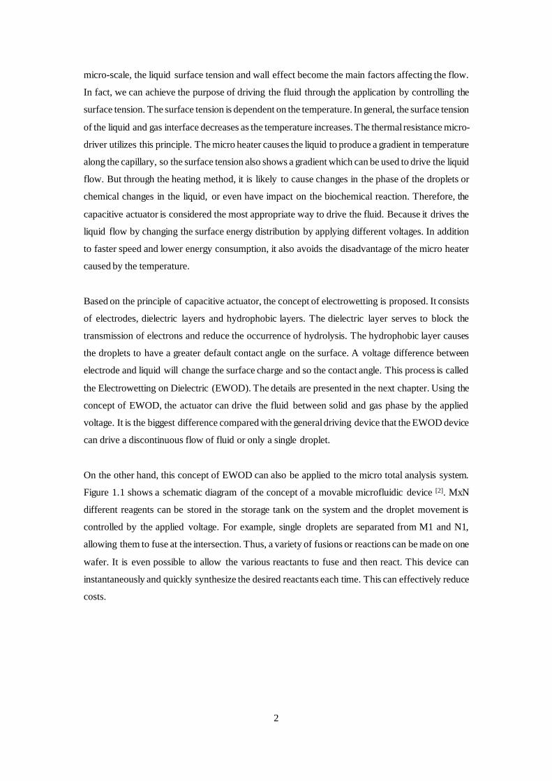
Figure 1.1 shows a schematic diagram of the concept of a movable microfluidic device [2]. MxN
different reagents can be stored in the storage tank on the system and the droplet movement is
controlled by the applied voltage. For example, single droplets are separated from M1 and N1,
allowing them to fuse at the intersection. Thus, a variety of fusions or reactions can be made on one
wafer. It is even possible to allow the various reactants to fuse and then react. This device can
instantaneously and quickly synthesize the desired reactants each time. This can effectively reduce
costs.

3
Figure 1.1 Mixing device of EWOD
It can be seen that EWOD has a wide range of applications. But many of the current studies are
based on high voltages. This allows some studies such as medical research, implantable devices, etc.
to receive a lot of restrictions. Research on low voltage driven droplet technology is a promising
future direction.
1.2 Objectives
The study described in this thesis is to develop on-chip valving and metering components based on
electrowetting of a (normally) hydrophobic channel segment, allowing automatic sample intake and
manipulation. Figure 1.2 shows a schematic of such an electrically operated valve. When a small
voltage is applied to the embedded control electrode the surface becomes hydrophilic and water will
flow through the valve. When the electrode is deactivated, the water will evacuate the valve area
due to the capillary pressure and the flow will stop. The hydrophobic air-vent channel allows air to
flow in and out during switching. A series of such valve segments can be used to accurately separate
a well-defined volume of fluid and transport it to the desired location on the chip for further
processing (e.g. analysis or mixing).

4
Figure 1.2 Schematic of electrowetting valve
1.3 Thesis outline
In chapter 2 the classification of the micropumps will be introduced. The theory of electrowetting
on dielectric and the three phases in EWOD will be explained. The designs of the EWOD devices
and the masks are explained in chapter 3. In chapter 4 the fabrication flow and some challenges are
described. Chapter 5 describes the simulation of flat type and the channel type of EWOD devices
and compares the outcomes with experimental results. Finally, chapter 6 present the conclusions
and suggestions.

5
Reference
[1] Morsink, D. W. "Design and Feasibility Test of a Microfluidic MEMS for an Integrated Light and
Scanning Electron Microscope." (2013).
[2] 微液滴驅動之研究與探討 (The study and discussion on Electrowetting) [D]. National Central
University, 2006.

6

7
Chapter 2. Micropumps and Electrowetting on dielectric overview
2.1 Micropumps
Microelectromechanical systems (MEMS) are devices that integrate mechanical components with
conventional electronic circuits on microchips. Due to the MEMS technology developing, a wide
range of sensors and actuators with very small size (micron level) have been invented and can be
used in both micro and macro world. Microfluidic device was the first MEMS device fabricated by
the technology that was intended to fabricate the microelectronic chips. Over the past few decades,
many microfluidic devices have been developed for flow sensors, pumps, valves, mixers and many
other devices.
This section briefly describes several working principle of micropumps.
2.1.1 Micropump classification
Over the past few years, several review articles have been published to evaluate micropumps for
their applications and performance. Some of them classify the micropumps according to their
working principle and other articles classify the micropumps by their design or performance.
Nguyen et al. [1] have reviewed many publications on micropumps and divided them into mechanical
and non-mechanical pumps. The mechanical pumps are divided into check-valve pump, peristaltic
pump, valveless rectification pump, rotary pump and ultrasonic pump. Non-mechanical pumps are
divided into electrohydrodynamic pump, electrokinetic pump, phase transfer pump, electrowetting
pump, electrochemical pump and magnetohydrodynamic pumps.
It should be noted that the classification only considers the working principle. The design and
performance of the same type of pump may be very different. Some designs are made in a single
silicon substrate, while other designs consist of other materials or two substrates. In addition, the
performance of the two pumps based on the same principle can be completely different. Pump
performance is mainly due to the design of the actual geometry and size.
In the next paragraphs, some common designs will be introduced.

8
2.1.2 Check-valve pump
The check-valve is the first micropump to be realized. Its working principle is basically the same as
the large pump. An actuator causes a stroke volume with two check valves that adjust the flow
direction. When the pump chamber is inflated and the chamber is filled, the inlet valve opens. The
outlet valve prevents the fluid from flowing back into the room. Then the pump chamber shrinks,
the inlet valve closes and the outlet valve opens due to the overpressure in the chamber. See Figure
2.1 [2].
Figure 2.1 Check valve
Over the past few years, different valve designs have been reported. But all valves are only allowed
to flow in one direction and prevent flow in the opposite direction. Some of the common designs of
check valves are: ring diaphragms, flaps and cantilever beams. The performance of the valve
depends to a large extent on the design of these things. The key features of the check valve are
reverse flow, pressure drop and switching speed.
2.1.3 Peristaltic pumps
The peristaltic pumps runs in the absence of a check valve for flow rectification. The principle is
based on the peristaltic motion of the pump chambers, which squeezes the fluid into the desired
direction. The volume can be pumped in either direction by starting the chamber with a phase
difference of 120°. The diaphragm of the chamber may also partially function as a check valve.
Typically, the chamber pressure in the peristaltic pump is lower than the chamber pressure in the
one way valve. Therefore, in the design of the peristaltic pump, the stroke volume and compression
ratio become more important parameters. It shows in Figure 2.2 [3].

9
Figure 2.2 Peristaltic pump
2.1.4 Electrohydrodynamic pumps
The electrohydrodynamic (EHD) pump is based on the electrostatic force acting on the medium
fluid. It can be divided into two main types: the EHD induction pump and the EHD injection pump.
The EHD induction pump is based on the induced charge at the material interface. The electric field
drags and pulls the induced charge along the wave direction. In the EHD injection pump, the
Coulomb force is responsible for the ion transportation from one or two electrodes by
electrochemical reaction. They are shown in Figure 2.3 [4].
Figure 2.3 (a) induction type; (b) injection type
2.1.5 Electrowetting pump
The principle of the electrowetting pump uses the tension between the solid / liquid interface to

10
remove the surface charge. This principle can be used for direct pumping. In recent years, more and
more people have studied electrowetting related things, electrowetting pump is no exception. In the
past decade, most people's research is based on several tens of volts to make the hydrophobic surface
changed to hydrophilic surface. Such high voltage cannot be used in the MEMS technology. But
recently the EWOD (Electrowetting on dielectric) based pump can drive the droplet at low voltage
and fast transferring speed. So by studying the characteristics of electrowetting to reduce the driving
voltage to make it a wider application is a trend.
2.2 Theory of electrowetting
In this section, the basic principles of electrowetting are introduced. There will be a theoretical
description of electrowetting and the formulas’ explanation. The three parts (dielectric layer,
hydrophobic layer and conducting fluid) that make up the entire EWOD system will be introduced
separately.
The standard EWOD device consists of electrodes covered with an insulating layer, conductive
droplets and a hydrophobic layer (Figure 2.4). In most applications, the droplet’s size is typically
less than or equal to 1 mm of water or solution. The external environment is usually air or other
liquid that is immiscible with the droplets, such as oil. In order to analyze the behavior of droplets,
the Bond number β is considered. It represents the relative magnitude of the force due to gravity
and interfacial tension:
(eq. 2.1)
In the equation, Δρ represents the density difference between the droplet and the surrounding
medium; g is the gravitational acceleration; R is the characteristic length of the droplet; and γci is
the interfacial tension between the conductive droplet and the insulating layer.

11
Figure 2.4 The classic schematic of EWOD (no applied voltage)
In a typical electrowetting system, especially when the droplets are in contact with the oil, β is much
smaller than unity [5]. So the gravity can be ignored. Therefore, in the absence of externally applied
voltage, the performance of the droplet will only be affected by the interfacial tension γ. The
contact angle which is formed by the conducting liquid (c), the external insulating environment (i)
and the dielectric substrate layer (d) is given by the Young’s equation [6]:
(eq. 2.2)
θY is the contact angle, it is also called the Young’s angle. γid, γcd andγci represent the interfacial
energy, respectively (Figure 2.5).
Figure 2.5 Balanced force distribution in an EWOD system with applied voltage

12
When an appropriate voltage is applied between the droplet and the bottom electrode (Figure 2.5),
the charge from the liquid is attracted to the droplet / hydrophobic interface. Assuming that the
liquid is a perfect conductor, its free charge density is zero. As can be seen from Figure 2.5, the
force generated by the liquid / hydrophobic interface charge has a vertical component. It causes
normal stress on the surface of the hydrophobic layer, which is compensated by elastic stress.
However, as the contact line approaches, the surface charge appears on the interface of the liquid /
hydrophobic layer due to sharp edge effects [7]. As a result, the electrostatic force F is generated in
the horizontal direction. The expression consists of the vacuum dielectric constant (ε0), the dielectric
constant (εr) of the dielectric, the applied voltage (V) and the dielectric thickness (d):
(eq. 2.3)
This electrostatic force will have an attraction to the droplets, resulting in a decrease in the contact
angle of the droplets formed on the hydrophobic layer. This contact angle is called the electrowetting
angle (θV) in the electric field. From Figure 2.5, the force balance on the horizontal axis can be
written as:
(eq. 2.4)
So the electrowetting angle can be obtained by combining equations 2.2, 2.3 and 2.4 as a function
of the applied voltage change [8]:
(eq. 2.5)
This is commonly referred to as Lippmann-Young’s equation. As long as there is no leakage in the
insulating layer, the droplet will return to its initial state when the voltage is removed.
In the derivation of the Lippmann-Young equation, the decrease in the contact angle is due to the
force generated by the electric field that acts on the liquid. In addition to this interpretation, there
are other different interpretations to describe the electrowetting effect. But all these explanations
finally get the same expression. In thermodynamics, as the potential differences increases across the
hydrophobic/droplet interface, charge builds up both at the solid electrode underlying the dielectric
layer and at the droplet, causing a decrease in interfacial energy [9].

13
Figure 2.6 The contact angle and the Young’s angle showing under the microscope
Nowadays, the ‘electromechanical explanation’ [10] has become to the most widely accepted
explanation. As shown in Figure 2.6, Mugele et al. [11] observed that the microscopic contact angle
is always maintained at the Young’s angle, although the macroscopic angle has become hydrophilic.
The theoretical prediction of small voltage is very consistent with the experimental results. However,
when the macroscopic contact angle reaches a certain angle as the voltage rises, it does not change
anymore. We call this angle that is no longer changing as a saturated contact angle.
Both DC and AC voltages can be used to drive the EWOD system. In the case where the applied
voltage is slowly changed, the contact angle and the droplet shape can instantaneously change to a
stable value. If the AC frequency is too high to exceed the fluid dynamic response time of the
droplets (typically millimeter-level droplets at frequencies of several hundred hertz), the liquid
response depends only on the time average of the applied voltage. This argument is correct, as long
as the basic assumption of the Lippmann’s equation is not violated: one of which is the liquid is a
perfect conductor. However, when the frequency is increases, the droplet decomposes. While the
dissolved ions can follow the applied field at moderate frequencies, they are not able to do so beyond
a certain critical frequency ωc. Far below ωc, the liquid behaves as a perfect conductor; far above it
behaves as a dielectric [5].

14
2.3 Three phases of electrowetting
As we talked about in section 2.1, a EWOD system consists of three phases: the conducting liquid,
the external insulating environment and the dielectric substrate layer.
2.3.1 The conducting liquid
In the classical theory of electrowetting, liquid is considered as a perfect conductor. For aqueous
salt solutions, this corresponds to the limits of high salt concentration or low frequency, as
previously described. The requirements for the concentration and nature of charge carriers are not
that strict. At low frequencies (f <1 kHz), even DI water shows significant electrowetting [12].
Typically, the salt, such as NaCl and sodium dodecylsulfate (SDS), concentration is 0.01-1 mol / L.
Most reports indicate that there is no significant effect due to the type or concentration of the salt.
Ion surfactants have another advantage. In addition to providing the charge required for the
electrowetting effect, it is possible to reduce the interfacial tension between the conductive droplet
and the insulating fluid. And according to eq. 2.5, the voltage required to reach the saturation angle
is reduced. However, Kuiper pointed out that if the reduction of γci is too large, it will affect the
switching speed, which is harmful to applications that need fast response [13].
2.3.2 The insulating environment
The insulating environment is generally composed of air or oil. The place where the gas environment
is applied is not particularly large because there is not much maneuverability. But on the contrary,
there are many applications using oil as an insulating environment.
2.3.3 The dielectric layer
For an EWOD system, the ideal situation is to get a large contact angle change using as low voltage
as possible. In order to achieve this goal, there are basically two ways according to eq. 2.5: increase
the Young’s angle or decrease the dielectric layer thickness.
In the EWOD system, aqueous solutions are the most commonly used conductive fluids. Therefore,
to get a higher Young's contact angle, different hydrophobic materials can be used. Ideally, the
dielectric itself is hydrophobic and pinhole free on its own (like PDMS, Parylene). Otherwise it is
necessary to deposit an insulating layer without pinhole under the hydrophobic layer.

15
The second way is to reduce the thickness of dielectric layer. As we can see from eq.2.5, the thinner
the insulating layer, the smaller the required voltage. But the thickness is limited by the breakdown
strength of the insulating material. When the electric field in the insulating layer exceeds the
breakdown strength, the molecular structure will be destroyed by the current generated in the
material. The dielectric breakdown voltage (Vbd) is a function of its thickness (d) and the dielectric
breakdown field strength (Ebd):
Vbd=Ebd·d (eq. 2.6)
So, on the one hand, the thinner insulating layer can achieve the same contact angle change with a
smaller voltage. But it also makes the breakdown voltage lower. According to eq.2.5, a higher
relative permittivity could also reduce the voltage needed.
Commonly used hydrophobic layers for low voltage EWOD include Cytop, Fluoropel, Teflon AF
and Parylene C. Wherein Cytop, Fluoropel and Teflon AF are amorphous fluoropolymer. They are
deposited by spin coating or dip coating and usually only as a hydrophobic layer rather than as a
main insulator. Parylene-C is a high quality pinhole-free polymer film produced by a vapor
deposition process. Comparing with other kinds of hydrophobic polymer, Parylene C has high
electrical insulating property and good mechanical strength. In order to increase the hydrophobicity
of the system, fluoropolymer can also be added to Parylene C.
Table 2.1 characteristics of the common EWOD materials [7] [14]

16
Common insulating materials in EWOD include silicon dioxide, silicon nitride, aluminum oxide
and tantalum pentoxide. Silicon dioxide (SiO2) is typically obtained by thermal oxidation of the
silicon substrate. Silicon nitride (SiN) is prepared using PECVD. Aluminum oxide is made using
the ALD (Atomic layer deposition) method. These are common materials in the microelectronics
industry. Since they are all hydrophilic, they must be coated with one of the above fluoropolymers
to achieve a hydrophobic effect. Most of these insulating materials have a high insulation breakdown
field strength, which allows us to use thinner insulation to reduce the required voltage.
Al2O3 is one of the most widely studied materials due to its excellent dielectric properties, thermal
stability and good adhesion to many surfaces [15]. In order to deposit pinhole free and very thin Al2O3
layer, atomic layer deposition (ALD) is one of the best methods. Especially the low-temperature
Al2O3 ALD films exhibited very low surface roughness values and low leakage currents. The root-
mean-squared surface roughness for a 1x1 um2 area averaged 4 ± 1 Å [16]. So it is chosen as one of
the dielectric materials for my low voltage EWOD application. The other insulating material used
in the application is silicon nitride. It can be seen from Table 2.1 that silicon nitride also has a high
dielectric constant and breakdown voltage. And the uniformity also can be well controlled during
the process [17].
2.4 Droplet transportation by EWOD
As described in the previous section, the benefits of using an insulating layer between droplets and
electrodes are very large. The presence of the dielectric layer not only allows the contact angle to
change even more, but also can be a good solution to solve the problem that a higher voltage will
cause fluid electrolysis. Because the number of the materials which can achieve the functions of
both hydrophobic and insulating is limited. And all of them have a relatively low dielectric constant.
If adding a special insulating layer with high dielectric constant, the constant of hydrophobic
material can be ignored since the presence of the insulating layer prevent them from break through.
According to e.q. 2.5, a larger dielectric constant results in a smaller voltage required when the
contact angle stays the same. The hydrophobic layer is only used for hydrophobic. And also because
of the pin-hole free insulating layer existing, there is no leaking current between the droplet and the
electrode as long as the voltage is lower than its strength. This can protect the device in a good way
and have a better performance.
By using this method, another innovation in EWOD is the use of patterned electrodes for droplet
transportation which is shown in Figure 2.7.

17
Figure 2.7 Schematic of EWOD transportation
Pollack et al. first used a few nanoliter to a few microliters of conductive droplets to show the droplet
transmission [18]. These droplets are located between two glass plates. The bottom plate has regular
electrodes covered by the dielectric and hydrophobic layers. The top plate has a continuous ground
electrodes, as shown in Figure 2.7. The conductive droplet is initially placed in the center of the
bottom electrode and sandwiched between the two hydrophobic layers. When proper voltage is
applied between the left bottom electrode and the ground electrode, the contact angle on the left side
of the droplet is changed according to eq. 2.5. When the applied voltage exceeds a certain threshold
voltage, the droplet moves to the left electrode where the voltage is applied. Pollack’s work was the
first demonstration of digital microfluidic lab-on-chip systems that use droplets instead of the
continuous microfluidic systems.
This process is shown in Figure 2.8 and Figure 2.9. The dotted line in the Figure 2.8 is the shape of
the droplet when no voltage is applied. After the voltage is applied on the left electrode, the droplet
shape changes to the solid one immediately. Figure 2.9, the filled droplet is the shape after it is
transported.
Figure 2.8 Immediately schematic of the drop when voltage applied on left electrode

18
Figure 2.9 Schematic of droplet after transportation
2.5 EWOD Related Applications
Michael et al. presented a micro-actuator to quickly process discrete micro droplets [19]. Micro
actuation is achieved by direct electrical control of surface tension of two opposing planar electrodes
which are fabricated on glass. A simple device consisting of a linear array of seven electrodes at 1.5
mm pitch was fabricated and tested. Droplets of 0.7 μL were successfully transferred between
electrodes at the voltage of 40-80 V. It has been shown that when the electrode switching rate is up
to 20 Hz and the average velocities is 300 mm/s, the droplets can be transported repeatedly. Figure
2.10 shows the video frames of the moving droplet. The view is from the top looking through the
ITO ground electrode. In the first picture, 80 V is applied on the electrode which is underneath the
droplet. In the second and third pictures, 80 V potential is applied on the electrode on the right of
the droplet and the droplet moves to that direction.
Figure 2.10 Video frames of the moving droplet
19
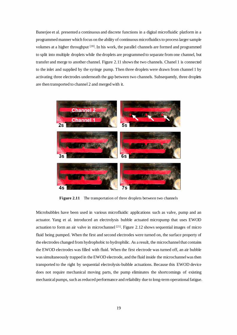
Banerjee et al. presented a continuous and discrete functions in a digital microfluidic platform in a
programmed manner which focus on the ability of continuous microfluidics to process larger sample
volumes at a higher throughput [20]. In his work, the parallel channels are formed and programmed
to split into multiple droplets while the droplets are programmed to separate from one channel, but
transfer and merge to another channel. Figure 2.11 shows the two channels. Chanel 1 is connected
to the inlet and supplied by the syringe pump. Then three droplets were drawn from channel 1 by
activating three electrodes underneath the gap between two channels. Subsequently, three droplets
are then transported to channel 2 and merged with it.
Figure 2.11 The transportation of three droplets between two channels
Microbubbles have been used in various microfluidic applications such as valve, pump and an
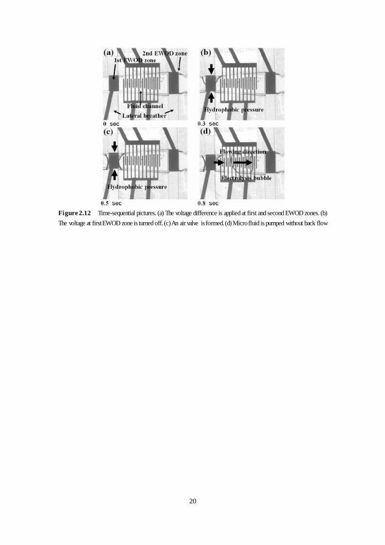
actuator. Yang et al. introduced an electrolysis bubble actuated micropump that uses EWOD
actuation to form an air valve in microchannel [21]. Figure 2.12 shows sequential images of micro
fluid being pumped. When the first and second electrodes were turned on, the surface property of
the electrodes changed from hydrophobic to hydrophilic. As a result, the microchannel that contains
the EWOD electrodes was filled with fluid. When the first electrode was turned off, an air bubble
was simultaneously trapped in the EWOD electrode, and the fluid inside the microchannel was then
transported to the right by sequential electrolysis-bubble actuations. Because this EWOD device
does not require mechanical moving parts, the pump eliminates the shortcomings of existing
mechanical pumps, such as reduced performance and reliability due to long-term operational fatigue.
20
Figure 2.12 Time-sequential pictures. (a) The voltage difference is applied at first and second EWOD zones. (b)
The voltage at first EWOD zone is turned off. (c) An air valve is formed. (d) Micro fluid is pumped without back flow

21
Reference
[1] Nguyen, Nam-Trung, Xiaoyang Huang, and Toh Kok Chuan. "MEMS-micropumps: a review." Journal of
fluids Engineering 124.2 (2002): 384-392.
[2] Meng, Ellis, et al. "A check-valved silicone diaphragm pump." Micro Electro Mechanical Systems, 2000.
MEMS 2000. The Thirteenth Annual International Conference on. IEEE, 2000.
[3] Wu, Min-Hsien, et al. "Development of perfusion-based micro 3-D cell culture platform and its application for
high throughput drug testing." Sensors and Actuators B: Chemical 129.1 (2008): 231-240.
[4] Iverson, Brian D., and Suresh V. Garimella. "Recent advances in microscale pumping technologies: a review
and evaluation." Microfluidics and Nanofluidics 5.2 (2008): 145-174.
[5] Mugele, Frieder, and Jean-Christophe Baret. "Electrowetting: from basics to applications." Journal of Physics:
Condensed Matter 17.28 (2005): R705.
[6] Young, Thomas. "An essay on the cohesion of fluids." Philosophical Transactions of the Royal Society of
London 95 (1805): 65-87.
[7] Chevalliot, Stéphanie. Advancing the Frontiers of Low Voltage Electrowetting on Dielectrics through a
Complete Understanding of Three Phases System Interactions. University of Cincinnati, 2012.
[8] Moon, Hyejin, et al. "Low voltage electrowetting-on-dielectric." Journal of applied physics 92.7 (2002): 4080-
4087.
[9] Welters, Wim JJ, and Lambertus GJ Fokkink. "Fast electrically switchable capillary effects." Langmuir 14.7
(1998): 1535-1538.
[10] Jones, Thomas B. "On the relationship of dielectrophoresis and electrowetting." Langmuir 18.11 (2002): 4437-
4443.
[11] Mugele, F., and J. Buehrle. "Equilibrium drop surface profiles in electric fields." Journal of Physics: Condensed
Matter 19.37 (2007): 375112.
[12] Jones, Thomas B., K-L. Wang, and D-J. Yao. "Frequency-dependent electromechanics of aqueous liquids :
electrowetting and dielectrophoresis." Langmuir 20.7 (2004): 2813-2818.
[13] Kuiper, Stein, and Benno Hendriks. "Voltage reduction in electrowetting-on-dielectric." Proceedings of ESA
annual meeting. 2005.
[14] Liu, Hong, et al. "Dielectric materials for electrowetting-on-dielectric actuation." Microsystem technologies
16.3 (2010): 449.
[15] Chang, Jong-hyeon, et al. "Low voltage electrowetting on atomic-layer-deposited aluminum oxide."
Nano/Micro Engineered and Molecular Systems (NEMS), 2010 5th IEEE International Conference on. IEEE,
2010.
[16] Groner, M. D., et al. "Low-temperature Al2O3 atomic layer deposition." Chemistry of Materials 16.4 (2004):
639-645.
[17] Liu, Liang, et al. "Study on the performance of PECVD silicon nitride thin films." Defence Technology 9.2

22
(2013): 121-126.
[18] Pollack, M. G., A. D. Shenderov, and R. B. Fair. "Electrowetting-based actuation of droplets for integrated
microfluidics." Lab on a Chip 2.2 (2002): 96-101.
[19] Pollack, Michael G., Richard B. Fair, and Alexander D. Shenderov. "Electrowetting-based actuation of liquid
droplets for microfluidic applications." Applied Physics Letters 77.11 (2000): 1725-1726.
[20] Banerjee, Ananda, et al. "Programmable electrowetting with channels and droplets." Micromachines 6.2
(2015): 172-185.
[21] Yang, Sang-Chung, and Cheng-Hsien Liu. "An Electrolysis-bubble-actuated micropump using electrowetting
on dielectric (EWOD) for 1XN micro-sample switches." Solid-State Sensors, Actuators and Microsystems
Conference, 2009. TRANSDUCERS 2009. International. IEEE, 2009.

23
Chapter 3. Design ideas
There are two different designs introduced in this chapter. One is a design with rectangular
electrodes of different widths compared with the air channel, the other one is a design of 45° angled
electrodes of the same size.
3.1 Different width electrodes and air channels
The main purpose of the entire design is to test whether the air vent valve based on electrowetting
technology works. So the whole device is mainly composed of four parts: water storage part, water
channel, air channel and electrodes. First the water in the tank will flow into the trench due to
capillarity and stop in front of the hydrophobic area. When the electrode under this hydrophobic
area is activated, the surface change into hydrophilic and the water flow continues to flow forward.
When the electrode is deactivated, the surface becomes hydrophobic again. But due to the existing
of the air channel, the surface tension is expected to force the liquid from the electrode area. The
overall schematic diagram of the first design is shown in Figure 3.1.
Figure 3.1 The schematic of the first design

24
As can be seen from Figure 3.1, there are two circular portions which are designed for water storage.
They are both surrounded by a hydrophobic layer to prevent the droplets from spreading over the
surface. The top one has a contact opening that is shown in the pink color because the water needs
to be connected to the ground. The red channel that links the two water storage sections is the trench.
As a precaution, it is surrounded by a hydrophobic layer. The width of the trench is 20um. The blue
ones are the electrodes, they also have the pink contact openings where we can apply the voltage.
Because the insulating layer is deposited on the entire wafer surface, there is no need for a specific
design. The contact openings are in the pink color.
As we can see from Figure 3.2, the trench is marked in red and air channel is in green. In order to
prevent the channel is blocked by some reason, a huge vertical (the vertical just looks from the
Figure 3.2 in green color) channel on the left to increase the area of contact with air. And of course
the whole air channel is covered by the hydrophobic layer to keep out the aqueous fluid. The
electrodes are deposited on the trench and connected to the contacting area. The part deposited on
the trench is covered by the insulating layer and hydrophobic material so the fluid flow can be
controlled by applying the voltage.
Figure 3.2 The specific design for trench and air channel

25
As mentioned before, the fluid should stop at the edge of the hydrophobic layer. When proper
voltage is applied on the electrode, the hydrophobic surface changes to hydrophilic and the fluid
continues to move forward. When the voltage is off, the fluid behind the electrode stops again.
Because of the presence of the air channel, liquid will withdraw from the electrode area. The portion
of the fluid which has already passed the electrode can continue to flow.
Figure 3.3 Specific design 1: trench (vertical red), air channel (horizontal red), electrode (blue) and
hydrophobic layer (yellow) and the relationship between them
So, three different lengths of electrodes were designed to test the behavior of the fluid. On the left
side of each electrode is an air channel covered with a hydrophobic layer. The width of the air

26
channel is slightly shorter, longer or equal to the length of the electrodes. So that it is possible to
observe whether the air channels of different lengths have an effect on the flow of the fluid. The
specific design of the electrode and air channel section can be seen in Figure 3.3, Figure 3.4 and
Figure 3.5. It should be noted that the vertical direction of the trench is continuous. That part is
covered by the blue electrode and yellow hydrophobic material. All units are microns.
Figure 3.4 Specific design 2: trench (vertical red), air channel (horizontal red), electrode (blue) and
hydrophobic layer (yellow) and the relationship between them

27
Figure 3.5 Specific design 3: trench (vertical red), air channel (horizontal red), electrode (blue) and
hydrophobic layer (yellow) and the relationship between them
It is a special design that was made different length of electrodes and air channels. Because when
the voltage disappears, the hydrophilic surface above the electrodes change to hydrophobic
immediately. There is still water remaining on the surface. Since it is difficult to exactly predict how
the fluid flow will behave during retreat from the electrodes, three different combinations of
electrodes and air channels were designed. After the equipment is manufactured, tests will show
how much the fluid remains on the electrodes after the voltage disappears.

28
Figure 3.6 Design of the water storage part
As can be seen from Figure 3.6, the diameter of the electrode is 2000um. The outer periphery of the
electrode is surrounded by a hydrophobic layer with a width of 50 microns to prevent liquid outflow.
The upper layer of the electrode is etched with a contact opening. So the fluid in this area will have
a good contact with the electrode that connects to the ground.
3.2 Oblique long electrodes
The main purpose of the entire design is to test whether the air vent valve based on electrowetting
technology works. So the whole device is mainly composed of four parts: water storage part, water
channel, air channels and electrodes. The overall schematic diagram is shown in Figure 3.7.
As can be seen from Figure 3.7, the overall structure design is roughly the same compared with
design 1. Two water storage portions are both surrounded by a hydrophobic layer to prevent the
droplets from spreading over the insulating hydrophilic surface. The difference compared with the
first design is both of the storage portions have contact opening showing in the pink color. The
reason is that this design would like to test two-way flow. The red channel that links the two water
storage sections is the trench. As a precaution, it is also surrounded by a hydrophobic layer. The
width of the trench is 100um. The blue areas are the electrodes. They also have the pink contact
openings where we can apply the voltage. Green parts are the air channels. Details are underneath.

29
Figure 3.7 The schematic of design 2
As we can see from Figure 3.8, the trench is marked in red and air channel is in green. In order to
prevent the channel from blocking, a huge vertical channel on the left to increase the area of contact
with air. The air channel near the trench section is covered with a hydrophobic layer to prevent the
fluid flowing in. The special designed oblique electrodes are deposited on the trench and connected
with the contacting area. The first part also overlapped by the insulating layer and hydrophobic
material to control the fluid flow by applying the voltage. Each air channel is designed in the upper
left corner of the electrode.
As mentioned before, the fluid is meant to stop at the edge of the hydrophobic layer. In this case,
the whole electrodes are all covered by the hydrophobic layer even the gap between the electrodes.
When proper voltage is applied on the electrode, the hydrophobic surface changes to hydrophilic
and the fluid continues to move forward. It stops at the edge of this electrode. When proper voltage

30
is applied on the next electrode, the fluid continues to flow even when there is a gap.
Figure 3.8 The schematic diagram of electrodes, hydrophobic layer and air channel
In Figure 3.9 and Figure 3.10, the design of all electrodes and air channels is presented. On the
upper left corner of each electrode the air channel is connected. The width of all air channels are 10
micron. It is possible to continuously observe the motion of the fluid on each electrode after the
voltage is switched off. It should be noted that the vertical direction (in the figures) of the trench is
continuous. That part is covered by the blue electrodes. And according to the theory of
electrowetting, all electrodes are covered by the insulating layer and yellow hydrophobic material.
All dimensions are in microns.

31
Figure 3.9 The specific design of electrodes, hydrophobic layer and air channel
Figure 3.10 The specific design of electrodes and air channel

32
The water storage portion 2 also has the pink contact opening as shown in the Figure 3.7. This is
because the fluid motion from water tank 2 to 1 is also something needs to know. After the electrode
5 is powered off, it will immediately become hydrophobic. But there is still water remaining on it.
The portion of the fluid that has flowed through the electrode 5 will continue to flow forward.
Because the air channel is hydrophobic and will provide the pressure the flowing needs. However,
the design can function both as a valve and as a precise metering system, so the motion of the fluid
remaining on the electrode is something needs to be find out. That’s why several electrodes are
designed to make sure what the measuring is accurate.
Figure 3.11 The specific design of top water storage portion and contact opening
From Figure 3.11, the diameter of the big circle electrode (blue one) is 900 micron. The outer
periphery of the electrode is surrounded by a hydrophobic layer with a width of 50 microns to
prevent liquid outflow on the hydrophilic surface. The upper layer of the electrode is etched with a
contact opening (pink). So the fluid in this area will have a good contact with the electrode which
connects to the ground. The opening is smaller than the designed electrode. This is to make sure
the contact openings are all efficient ones.
3.3 Mask design
All the devices will be made on top of the silicon wafer. However, due to its small size, it is necessary
to use a microfabrication process. So, one of the most efficient and reliable techniques to allow for
very precise engraving of very small features is lithography. There will be a complete explanation

33
in the manufacturing section (Chapter 4). It is important here to know that such a process requires
the use of a mask through which the portion of the target is selectively exposed to ultraviolet light.
However, the shape of the mask defines the contour to be printed. In addition, since the photoresist
used in the cleanroom could be positive or negative according to the different processes, the part
transferred into the mask is designed to be transparent or non-transparent. With this in mind, the
masks are designed according to the different processes and solve the problems encountered.
There are different precision in the mask printing technology. In out cleanroom EKL, the minimum
resolution is 5 micron. And in my design, the smallest gap showing in Figure 3.10 is 8.53 microns.
So there is a safe margin and avoid any problems in this regard.
After determining the design and all the requirements in designing the mask, the designs need to be
converted to the mask in order to fabricate the device in the cleanroom. The entire device consists
of five layers, namely: trench layer, electrode layer, insulating layer, hydrophobic layer and contact
opening. The trench layer includes channels for liquid flow and air channels. Because the entire
device is fabricated on a silicon wafer, the micron-level depth of the channels are obtained by
etching silicon. For the insulation layer, the silicon nitride or aluminum oxide is deposited on the
entire wafer. So for this step, no mask is needed. In the contact opening step, the portion of the
insulating layer where the voltage is applied to the electrode is etched away.
Figure 3.12 Mask layout, the dimensions are on the mask level

34
Figure 3.12 shows the mask layout. The dimension is in the mask level which is 5 times larger than
the actual size in the designs. The reason why it is designed like this will be explained in the next
chapter. From Figure 3.13, number 1-4 are the masks of design 2 and number 5-8 are the masks of
design 1. The number 5 to 8 are trench, electrodes, contact opening and hydrophobic layer,
respectively. The number 1 to 4 are also trench, electrodes, contact opening and hydrophobic layer,
respectively. It should be noted that my project is in conjunction with someone else’s project, so not
all things in the picture are my design. And why I designed some of the parts solid and some parts
designed into a hollow I will detail in chapter 5. This is a choice in fabrication.
Figure 3.13 The overall diagram of mask

35
Chapter 4. Fabrication Process
In the previous chapters, the principle of electrowetting and design ideas are explained. In this
chapter an overview of the silicon microfabrication technique and the fabrication flow are presented.
4.1 The fabrication method
In order to fabricate the device using silicon microfabrication techniques, there are some objectives:
The fabrication of the micro channels must be accurate and the side walls should be vertical.
The metal on the side walls must be uniformly deposited.
The pattern of the metal inside the channel must be intact.
The hydrophobic layer should have a uniform thickness, also on the sidewalls.
A schematic of the steps of the fabrication process is presented in Figure 4.1. First a 2000 nm thick
silicon oxide layer is deposited on the silicon wafer. Then in the areas where the trenches and the
air channel need to be fabricated, the silicon oxide layer is etched by plasma etching. After that, the
trenches and the air channel are etched into the silicon using reactive ion etching (RIE). Meanwhile,
the remaining silicon oxide layer is used as a mask layer to prevent the silicon outside the trenches
and air channel to be etched. The mask layer of SiO2 is then removed by wet etching using BHF
leaving the trenches and the air channel on the wafer. In order to prevent the direct contacting of the
silicon and the electrodes, a 500 nm insulating SiO2 layer is added on the wafer. After that 200 nm
thick metal is deposited and patterned on the SiO2. Then the whole wafer is covered by an insulating
layer of SiNx or Al2O3. Then the contact openings are etched after which the hydrophobic layer is
deposited and patterned.
The advantage of this microfabrication method is that the various features of the same portion in the
design can be included in one single image of the mask to be fabricated. For example, the depth of
trench depends on the time of etching but the shapes are all the same. So there is no need to design
different masks for different depths of trenches.

36
Figure 4.1 The fabrication process flow

37
4.2 Fabrication process flow
4.2.1 Cleaning Wafers
The very first step after opening a box carrier containing a new batch of silicon
wafers, is cleaning the wafers before the start of the process. This to remove any
contamination and to clean the wafer. Because the surface of the wafers could
be contaminated or is not clean enough after being kept in the plastic box carrier
for some time. A process named ‘cleaning line’ is needed for the cleaning. Figure
4.2 depicts an overview of the cleaning process.
4.2.2 Zero Layer
At the beginning of the whole process, the first processing step to a wafer is the zero layer. This
includes the alignment marker and wafer ID. The alignment marker is a necessity during the
photolithography process to make sure the wafer is exposed in the right position. Wafer ID is to
ensure that each piece of wafer is numbered to prevent the mess.
4.2.3 PECVD Silicon Oxide Deposition
After the cleaning process, a layer of SiO2 with a thickness of 2000 nm is deposited on the wafer. It
is used as a mask layer for the process of silicon etching. The method chosen for SiO2 was Plasma
Enhanced Chemical Vapor Deposition (PECVD). At 400 ℃ the deposition parameters have been
optimized to deposit a flat oxide layer without pinholes. The reason why choosing such a thickness
is that it’s important to protect the rest of the silicon from being etched during the trench etching
process. The biggest depth of the trench is 50 μm and the selectivity between silicon and silicon
oxide is 100: 1. To ensure that no silicon other than the trench is etched, the thickness is selected as
2000 nm. And the deposition time is 23.5 seconds. This is why the PECVD process is selected.
Comparing to a few hours of LPCVD processing time, 23.5 seconds is much faster.
4.2.4 Coating, Lithography and Development
A layer of positive photoresist is deposited on the silicon oxide. After baking, the patterns defining
the trenches are transferred from the photomask to the wafer with lithography. Photoresist is exposed
to the patterns using a wafer stepper. The photoresist is then developed and the areas that were
Figure 4.2 Figure 4.2
Cleaning step

38
exposed are dissolved in the developer and removed while non-exposed areas remain and the pattern
is transferred as can be seen in Figure 4.3.
Figure 4.3 Wafer in lithography process and after development
Spin coating is a procedure used to deposit uniform thin films to flat substrates. Usually a small
amount of coating material is applied on the center of the substrate, which is either spinning at low
speed or not spinning at all. The substrate is then rotated at high speed in order to spread the coating
material by centrifugal force. The coating and developing machine used in EKL cleanroom is EVG
120 coater and developer. The spinning process is shown in Figure 4.4.
Figure 4.4 Coating photoresist using EVG 120 [1]
Rotation is continued while the fluid spins off the edges of the substrate, until the desired thickness
(usually 1-3 um) of the film is achieved. The applied solvent is usually volatile, and simultaneously
evaporates. So, the higher the angular speed of spinning, the thinner the film. The thickness of the
film also depends on the viscosity and concentration of the solution and the solvent. Usually, the

39
thickness of photoresist should be taken into consideration because of the etching and exposure
resolution. The smallest patterns were 5 um. The photoresist used could not be too thick as thicker
layers will limit the resolution. And because of the development process, the photoresist cannot be
too thin either. In this case a thickness of 2.1 μm was chosen.
After the prebaking, the photoresist is exposed to a pattern of intense light in the lithography
machine. The exposure to light causes a chemical change that allows some of the photoresist to be
removed by a special solution, called ‘developer’. Positive photoresist, the most common type,
becomes soluble in the developer when exposed; with negative photoresist, unexposed regions are
soluble in the developer. After the development process, the required pattern appears on the wafer.
The whole process is shown in the first four steps of Figure 4.6.
The lithography machine used in the EKL cleanroom is ASML PAS5500/80 waferstepper. The
photomask is located above a high resolution lens. The Cr-side of the mask is facing down to the
lens and the features on the mask are imaged through the lens on to the wafer. Obviously, all images
on the mask should be placed in the waferstepper’s available image area, which is 105*105 mm2 on
mask level. The reduction factor of the lens is 5, so the pattern on the mask is 5 times larger than
the pattern on the wafer. In addition, due to the requirement of EKL, the images should be separated
by a distance of 5 mm. This means that nine 30*30 mm2 images can be accommodated in the
waferstepper’s image area. See Figure 4.5 [2].
Figure 4.5 Mask layout

40
4.2.5 Plasma Etching Silicon Oxide
After the patterns are exposed and developed, the exposed areas of silicon oxide are plasma etched.
The process pressure applied is 180 mTorr and the RF power is 300 W. The gasses & flows
environment of C2F6/CHF3 is 36/144 sccm and the He pressure is 12 Torr. To ensure that all silicon
oxide is etched away, overetch is required. That means that some of the silicon on the trench location
is also etched. After the etching, the height difference between the remaining silicon oxide and the
trench portion was measured. By comparing with the remaining thickness of the silicon oxide layer,
it shows how much of the silicon in the trench is removed by the etching process. The average
thickness of silicon oxide layer left is 1600 nm and the height difference is 1660 nm. So the silicon
is etched about 60 nm which can be neglected compared to the compared to the 20 um depth of the
trenches. The process is shown in the last 3 steps of Figure 4.6 [3].
Figure 4.6 Coating, lithography, development and plasma etching process
4.2.6 Deep Reactive Ion Etching (DRIE)
After the silicon oxide is patterned, the exposed silicon is etched using plasma etching. The
technology used is Deep Reactive Ion Etching (DRIE) using the Bosch process, where the SiO2
layer serves as the mask layer. The selectivity between silicon and silicon oxide is high so there is
no need to worry about the SiO2 layer being etched away.

41
Bosch Process: Deep etching with repeated cycles of etching and passivation. First the silicon is
etched with a mix of SF6 and 10% O2, and then the sidewalls are passivated with C4F6. The cycle
is then repeated. Longer cycles mean faster etchrate but bigger scallops on the sidewalls. The size
of the opening in the mask directly influences the speed of DRIE. Very small openings in the mask
result in a rapidly decreasing etch rate as the etch depth proceeds. In this case, the trench width is
100 μm and the depth is 20 μm. So there is no need to worry about this issue. The whole process is
shown in Figure 4.7.
Figure 4.7 Bosch Process of DRIE [4]
4.2.7 TEOS Silicon Oxide Deposition
Before the metal deposition, a silicon oxide layer is deposited on the wafer to prevent the contact
between metal and silicon. LPCVD TEOS is a common way of depositing silicon oxide. TEOS
(tetraethylorthosilicate, Si(OC2H5)4) is the source for silicon oxide and the reacting temperature is
around 650℃ to 750℃ and it produces a relatively pure oxide [5].
The recipe used in the furnace of EKL is: TEOS bubbler (40℃); 250 mTorr pressure; 700 ℃. After
1h 7min deposition, a 488 nm thick oxide layer was obtained.

42
4.2.8 Spray Coating
To pattern the metallization layer a lift-off process will be used. Which means that a photoresist and
a lithography step have to be applied prior to metal deposition. Because of the existence of the trench,
the wafer cannot be coated by spin coating. Otherwise this will lead to uneven distribution of
photoresist in the trenches and cannot be fully developed. Instead of spin coating, spray coating is
used. The spray method is to spray the photoresist from the edge of the wafer slowly to the middle.
Meanwhile, the wafer is slowly rotating to make sure the photoresist is evenly coated on the surface
of the wafer. The photoresist on the wafer is not as uniform as coated by spin coating, it is thinner
at the edge and thicker at the center. However, this can be solved by over exposure during the
photolithography process.
First the photoresist needs to be changed to the negative one because of the pattern in the mask.
Then select recipe “HP-1000mbar-2mL-8 layers” on the user interface as shown in the Figure 4.8.
After the pre-aligner falling down, put the wafer on the coat module and then the spraying module
start to work. The recipe will form a 2-3 μm thickness photoresist layer after 8 times spray coating
with 2 mL diluted nLOF 2070 negative photoresist. Once it is finished, the wafer needs a 15 minutes
bake at 100℃. The next steps are photolithography and development. Because there is no existing
recipe for spray coating with trenches, manual development is needed. The wafer is treated with
“322 developer” in a beaker and shaken slowly. The photoresist gradually disappeared from the
edge to center.
Figure 4.8 Spray Coater [6]

43
During the spray coating process, different thicknesses were tested. A triple deposition according
the aforementioned standard recipe showed hard to develop. The structures on the edge disappeared
during the development process while the photoresist in the middle was not removed. But during
the process, it was found that 1 layer of spray coated photoresist is relatively uniform and pin-hole
free. After development all structures were perfectly preserved.
4.2.9 Metal Evaporation
After definition of the metal pattern in photoresist, the metal is deposited on the wafer. The
technology used in this process is metal evaporating deposition and the machine is CHA Evaporator.
The CHA Evaporator is an electron beam metal evaporator with the capability of coating several
wafers at the same time. It can control the metal deposition automatically with angstrom level
accuracy.
Figure 4.9 and Figure 4.10[7] show the inside of the evaporator. The wafers are placed face down on
the tray and secured. Once the program is started, it becomes highly vacuum. Then the source is
heated and evaporation starts. The tray will be rotating to ensure uniform deposition. Because there
is still photoresist on the wafer, the temperature inside the machine cannot be too high otherwise it
will destabilize the photoresist on the wafer. So once the temperature reaches 80℃, the machine
needs to be stopped by hand and cooled down to 60℃.
Figure 4.9 Wafer tray in CHA (face down)

44
Figure 4.10 Source of metal and electron gun
The recipe for metal deposition is 20 nm Ta and 180 nm Pt. The adhesion of Pt to silicon oxide is
not good enough, therefore, an intermediate adhesion layer is required. First Ti was used, but it
showed to have insufficient adhesion leading to loss of metal pattern after lift-off, as shown in Figure
4.12. A 20 nm Ta adhesion layer under 180 nm Pt showed better performance. For the lift-off process
the wafer was submersed in a beaker with 70℃ NMP (a developer to dissolve the photoresist) until
the photoresist was fully dissolved (see Figure 4.11). Then the wafer was dried and put into the
Tepla machine to have an oxygen plasma treatment. After the metal deposition process, the wafer is
contaminated and needs to put it into a special box.
Figure 4.11 Lift-off process

45
Figure 4.12 Loss of metal pattern after lift-off due to bad Ti adhesion.
4.2.10 PECVD Silicon Nitride
In this step, a thin silicon nitride layer is deposited on the wafer using PECVD. The purpose of this
layer is as an insulating layer for electrowetting. The thickness is determined according to the
experiment and the only difference for different thickness is the depositing time. At 400℃, the
deposition parameters have been optimized to deposit a uniform silicon nitride layer without pin-
holes. The recipe we use is as follows:
Gasses & flows: N2/SiH4/NH3=100/280/1800 sccm.
Pressure: 2.8 Torr
HF power: 320W
LF power: 480W
The depositing rate is 30 nm/s which is known from the previous experiments. After calculation, if
100nm silicon nitride is needed, the deposition time is 3.2 seconds. By measuring the thickness of
silicon nitride on the test wafer, the thickness of silicon nitride on the wafer which have structures
on it is known and the thickness is 102 nm.
4.2.11 Hydrophobic Layer Deposition
Two hydrophobic materials are considered to create the hydrophobic top-layer: Parylene and
FluoroPel.
Parylene is a common used hydrophobic material. It is deposited by vapor deposition in EKL MEMS
lab. The machine shows in Figure 4.13. In order to get a thin layer, 1 gram Parylene is used and the

46
thickness realized is 588 nm. This is the minimum thickness that can be achieved in EKL. Because
the ideal thickness for the electrowetting device is less than 100 nm, it needs to be etched back by
oxygen plasma etching.
Figure 4.13 Parylene deposition
Figure 4.14 Contact angle of Parylene after deposition.
The contact angle before etching is shown in Figure 4.14. After the plasma etching, the surface of
Parylene is ionized and loses its hydrophobicity with the contact angle of 79°. In fact it has become
super hydrophilic and it is almost impossible to measure the contact angle. Then a special chemical
of thiol end organic compound is mixed with Isopropyl Alcohol at the ratio of 1:100. The purpose
is to form a molecular film on the surface of Parylene. But the result is not very satisfactory. Despite
the improved hydrophobicity, the contact angle is still only 31 degrees. The result shows in Figure
4.15 and Figure 4.16. So the result of this experiment shows that a proper hydrophobic Parylene
layer can only be achieved without back etching.

47
Figure 4.15 Droplet on the wafer after the treatment
Figure 4.16 Contact angle after the treatment
Because what is needed is a hydrophobic layer, so another method is tried to make the surface
hydrophobic again. From literature [8], a plasma treatment with CF4 can result in a lager contact
angle even if the surface has already changed into hydrophilic. The recipe is as follows: 20sccm
CF4; 20 W; 10 seconds. After the treatment, the contact angle change into 108° which is shown in
Figure 4.17.

48
Figure 4.17 Contact angle of Parylene after CF4 treatment
Fluoropel is a new hydrophobic material fabricated by CYTONIX. It comes as a one percent
fluoropolymer solution in a fluorosolvent (BP=160℃). The contact angle to water is 110 degree as
shown in Figure 4.18. This is an ideally hydrophobic material for the experiment. The method of
coating it on a wafer is: first let the wafer rotate slowly and drip the Fluoropel on the wafer;
accelerate the rotation speed to 3000 rpm for 1 minute; put the wafer on the hot plate at 80 ℃ for
10 minutes and then 10 minutes at 160°C. The thin film dries in 4-6 hours at room temperature to a
surface energy of about 16 dynes/cm. Heating up to 160℃ for 30 minutes could optimize adhesion
and reduce the surface energy to about 10 dynes/cm.
Figure 4.18 Contact angle to water

49
After the spin coating of Fluoropel, the wafer needs to be coated by negative photoresist. First, a
standard spin coating process is tried and it turns out that there is no photoresist on the wafer because
the Fluoropel is super hydrophobic. The negative photoresist does not stick to it. Then the spray
coating negative photoresist method is tried. After coating with the recipe of “HP -1000mbar-2ml-
8layers”, the wafer is checked under a microscope. It is found out that there are a lot of pin-holes
on the wafer as shown in the Figure 4.19. After 3 times of spray coating, the pin holes have basically
disappeared except at the center. The wafer then went through photolithography and manual
development to achieve the patterns that can be plasma etched.
Figure 4.19 Surface of the wafer after one time spray coating
The machine used for plasma etching is Alcatel GIR300 F etcher. And the recipe is as follows:
O2: 70 sccm
Power: 60 W
It is an oxygen plasma etching. Because the other materials like SiNx and Pt are not etched by this
method, the wafer can stand over-etching to remove the Fluoropel completely. Then the rest of the
photoresist on the wafer is removed by acetone. The remaining part, as can be seen from the Figure
4.20, is still hydrophobic. A lot of experiments were done before finding a feasible solution, but the
results were not satisfactory. This is the best way that can be achieved in EKL using the spray coater
and the result seems good.

50
Figure 4.20 Hydrophobicity after oxygen plasma etching
The reason why the result of coating is not good enough is because the photoresist is not sticky
enough. When the spin speed is high, the photoresist is thrown out rather than stuck on the wafer.
So the Nlof 2070 is used which is super sticky. First fully coat the wafer with Nlof 2070 and then
use a low accelerate rate to reach the spinning speed of 3000 rpm. The recipe shows in Figure 4.21.
After coating, bake the wafer for 2 minutes at 100℃ then go to the photolithography. In this way,
the wafer is well patterned and can be developed well.
Figure 4.21 The recipe of coating Nlof 2070 on FluoroPel
Other methods to pattern the Fluoropel, like lift-off techniques, have been researched as well.
However none of them showed satisfactory results.

51
4.2.12 Dicing and Bonding
The last two steps for the chip are dicing and bonding. First the wafer should be put on a foil. The
dicing used is a 40 μm blade with high pressure water gun to scour the residue from dicing. After
alignment, the dicing is done automatically. Figure 4.22 shows the wafer after dicing.
Figure 4.22 The wafer after dicing
After pick some good chips from the diced wafer, they need to be bonded with gold lines. The
bonding process is to connect the contact pads of the chip to the substrate in order to easier the
testing process. Figure 4.23 shows the chips after bonding and Figure 4.24 shows the two bonding
methods of two designs.
Figure 4.23 The chips after bonding
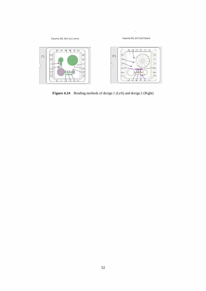
52
Figure 4.24 Bonding methods of design 1 (Left) and design 2 (Right)
53
Reference
[1] https://www.youtube.com/watch?v=4FCeKf4deiU
[2] Multi image mask exposure job description - Henk Van Zeijl (2016)
[3] Kiani, Amirkianoosh, et al. "Maskless lithography using silicon oxide etch-stop layer induced by
megahertz repetition femtosecond laser pulses." Optics express 19.11 (2011): 10834-10842.
[4] Dahar, S. "A New Method For Fabrication of Medical Microfluidic Devices." (2016).
[5] Cale, T. S., and G. B. Raupp. "A unified line‐of‐sight model of deposition in rectangular trenches." Journal
of Vacuum Science & Technology B: Microelectronics Processing and Phenomena 8.6 (1990): 1242-1248.
[6] http://mfz140.ust.hk/Eq_manual/EVG%20101%20Spray%20Coater%20Operation%20Manual.pdf
[7] https://www.utdallas.edu/~rar011300/CHAevap/CHAmanual.pdf
[8] Yeh, Fu-Wen, et al. "The arrowed surface ratchets with hydrophobic parylene for droplet transportation."
Nano/Micro Engineered and Molecular Systems, 2009. NEMS 2009. 4th IEEE International Conference
on. IEEE, 2009.

54

55
Chapter 5. Simulations and Measurements
Comsol Multiphysics simulation is used to estimate the performance and assist in the design of the
device before fabrication. It can give us a rough idea of the experimental process, including how
much voltage will result in contact angle saturation. Then the measurements performed on the
fabricated devices are described.
5.1 Simulations
The purpose of this simulation is to look at the relationship between the thickness of the insulating
layer and the voltage. According to the theory of electrowetting, the contact angle of water will
change when there is voltage applied. But the contact angle does not diminish indefinitely, it will
have a saturation angle. By simulation, varying voltages can be applied to the electrode under the
insulating layer to follow the change in contact angle. Multiple simulations can be run for different
insulating materials and layer thicknesses. In this way, the relationship between the thickness and
composition of the insulating layer and the value of voltage to reach the saturation contact angle can
be found.
5.1.1 Simulation of the Classic Model
The simulation on a flat type wafer is to verify the feasibility of electrowetting and how much the
angle of change will be given a certain voltage applied in the experiment. The first method used to
simulate is the level set method which is also the most common one. The basic illustration is shown
in Figure 5.1. This is a basic structure of electrowetting which consists of electrodes, a droplet, a
hydrophobic layer and an insulating layer.
Figure 5.1 A schematic of the electrowetting geometry

56
This model aims to simulate the movement of the interface between two immiscible phases by using
the level-set method with Navier-Stokes equations [1]. The behavior of the interface is controlled by
the surface tension of the two phases. Also, the wetting properties of the two fluids can be described
by calculating for the contact angle. In this case, the parameters in this simulation can be changed
easily, like the applied voltage, the thickness of insulating layer, etc.
In this simulation, once the parameters of the material and the voltage is set up, the shape changing
of the droplet with time can be simulated by Comsol which used a voltage sweep of 1V, 2V, 3V to
get some more results in one simulation. Figure 5.2 shows the output of the simulation with 3V. For
the insulating material, Si3N4 is chose with the dielectric constant of 7.5 and a thickness of 80 nm.
The total time of simulation is 0.2s.
Figure 5.2 Simulation results over time

57
The initial droplet is shaped with a black line. When the voltage is applied, the surface changes to
hydrophilic and the contact angle is obviously less than 90°. From this simulation, the shape
changing of the droplet can be seen very clearly. When the time reach to 0.12s, the shape changing
basically stopped and after that it only has some small modification. The angle change is really fast
even when the applied voltage is smaller than 3V which will be shown below. For the applied
voltages 1V, 2V, 3V, the times for the droplet to reach the saturation angle are all 0.16s, see Figure
5.3.
Figure 5.3 Time required of droplet reaches the saturation angle
5.1.2 Simulation of the Channel Model
The purpose of this project is to control the flow of fluid through a channel by switching it on and
off. So the simulation of the fluid in a channel is needed. In this simulation, there is no voltage
applied on the electrode at first and the surface is hydrophobic. Once the electrode is energized, the
contact angle will be reduced to hydrophilic. And because of the charge attraction, water will
continue to flow to the edge of the energized electrode. The initial contact angle is 140° and the
dielectric layer thickness is 50 nm with the dielectric constant of 9. The hydrophobic layer is set as

58
50 nm with the dielectric constant of 2.7. With the applied voltage of 10V on both sides of the 200
μm width channel, the simulation process is shown in Figure 5.4. The angle changing is really fast
within 0.02s and the fluid starts to flow forward after that. It can be seen from this phenomenon that
the water in the channel can be driven forward by applying proper voltage.
Figure 5.4 Simulation of the channel model

59
5.2 Measurements
5.2.1 Measurement on Flat Type Wafer
The measurement on the flat type wafer aims to test whether the theory of electrowetting works.
The setup of this experiment is very simple, and basically the same as the classic electrowetting,
composed of droplet, electrodes, hydrophobic layer and insulating layer as shown in Figure 5.1. The
insulating layer is 102 nm or 155 nm silicon nitride and the bare silicon substrate is used as the
electrode. The whole wafer is covered with a 27 nm thick FluoroPel hydrophobic layer.
The initial contact angle of DI water on the FluoroPel layer is 108° as shown in the Figure 5.5. The
first measurement used a 155 nm silicon nitride layer. The needle is inserted in the droplet as a
ground electrode as shown in the Figure 5.6 which is the initial state of this experiment. When the
voltage rises to DC 10V, the droplet starts to change and the contact angle changes to around 90°
when the voltage reaches 12V. At a voltage of 25V there will be a sudden great change that the
contact angle has a big change, probably because the shape of the tip is asymmetric. Once the droplet
leaves the non-uniform part of the tip, there will be a large change. The smallest contact angle
happens when the voltage reaches approximately 30V as shown in Figure 5.7. If the applied voltage
changes to 32V, the insulating layer is broken through and gas bubbles can be seen inside the droplet.
Figure 5.5 The contact angle of DI water droplet on FluoroPel layer

60
Figure 5.6 Initial state of the droplet
Figure 5.7 The shape of the droplet at 30V
The second measurement happens on the wafer with 102nm silicon nitride. The initial contact angle
of DI water to FluoroPel is the same of 108° which can be seen from Figure 5.8. But due to the
thinner insulating layer, the driving voltage should also be lower either. In this experiment, the
droplet starts to have some shape changing when the voltage is 6V. The significant shape changing
happens at about 15V (Figure 5.9) and the maximum angle is observed at 18V.

61
Figure 5.8 Initial state of the droplet with 102 nm SiN
Figure 5.9 The shape of droplet at 15V
Figure 5.10 The droplet jumps away at 18V

62
When the voltage is larger than 18V, the droplet jumps away from the needle and loses the contact
with the potential as shown in Figure 5.10. Then it re-form to the initial shape within 3 seconds.
Because of this performance, the saturation state of electrowetting on this wafer cannot be observed.
But the contact angle of 18V is pretty small around 40°. According to the experiment result on the
155nm silicon nitride wafer, it can be estimated that the contact angle at 18V is basically the
saturation angle. Because the droplet jumps away, there is no breakthrough to be observed on this
wafer.
5.2.2 Measurement on the Chip
The silicon wafer is diced into separate chips, each having the designed electrowetting structures on
it. After packaging and bonding, the chip can be tested on a printed circuit board to which the
external test voltages can be applied, as shown in Figure 5.11. The first experiment is to test whether
the electrowetting theory works on the designed structure with parylene as hydrophobic layer. For
this a special circular test structure with interdigitated electrodes was used. A tiny droplet of DI
water was dropped on the chip and the droplet stays in a hydrophobic state. After applying voltage
on the electrodes, the shape of the droplet starts to change but not as much as expected, see Figure
5.12. After applying a DC voltage of 35V on the electrodes, the droplet spreads out a little bit but
not very obvious. During the measurement, the parylene seems to lose its hydrophobicity. This also
could be one of the reason that the shape changing is not obvious. If the voltage goes any higher,
the insulating layer is breaks down and gas bubbles become visible inside the droplet.
Figure 5.11 Bonded chip

63
Figure 5.12 No voltage (left); 35V (right)
5.2.3 Measurement on the Probe Station
Since the dicing and bonding process really takes time, the measurements were performed on the
whole wafer on a probe station. This has the advantages of greatly reducing the preparation time of
the experiment while measurements can be done on any chip on the wafer. The setup of this probe
station is shown in Figure 5.13 which use vacuum suction to stabilize the wafer and use probes
needles to apply voltage on the contact pads of the chips.
Figure 5.13 Probe station setup
First the wafer with 88nm silicon nitride as the insulating layer and FluoroPel as the hydrophobic
layer is measured. The hydrophobicity of FluoroPel is good and the initial contact angle is 108°.
When the voltage is slowly applied on the contact pad, the shape of the droplet starts to change.

64
Figure 5.14 shows the shape changing of the droplet from which can be seen that there is small
change on the edge of the droplet. When the voltage goes higher than 23V, the insulating layer
breaks through and gas bubbles appear.
Figure 5.14 The shape changing from 0V (left) to 20V (right)
Then the wafer with 30nm Al2O3 as the insulating layer is used to observe the shape changing under
the microscope. First the DI water with NaCl is used. When the DC voltage is used, it easily breaks
through with a low voltage. There is a small changing with 10V AC voltage but the voltage cannot
go any higher. Then the pure DI water is tried. With AC voltage, there is no big changing when it
goes to the maximum of 10V. But when the DC voltage rises to about 17V, the shape starts to change
until the insulating layer breaks down at 22V. The shape changes a little during the potential rising
but not as much as expected.
The reason the droplet shape does not change much could be the big surface tension. So 1% SDS
solution is used to reduce the surface energy. First the 100Hz AC voltage is tried and which shows
a small change at 10V. Since the AC source cannot supply higher voltage, DC voltage is applied on
the two electrodes. With this combination, the shape starts to change at 7V and get the biggest
changing on 23V as shown in Figure 5.15. From the right picture below can be seen that the shape
changing is not circular. It shows a regular deformation consistent with the electrode structure. Since
the droplet change is very small compared to the tests on the flat wafer it can be concluded that the
interdigitated electrode structure is not very suitable for electrowetting tests.
When the voltage reaches 25V, the insulating layer breaks down. This damage is permanent and
doesn’t recover when the voltage is removed.

65
Figure 5.15 Shape changing from 0V (left) to 23V (right)
From these experiments, it can be seen that the reliability and stability of FluoroPel is much higher
than that of Parylene. Although the Parylene becomes hydrophobic again after the CF4 plasma
treatment, but it is really not stable. In contrast, FluoroPel retains its initial hydrophobicity after
many different tests. What’s more, the contact angle changing on the top-bottom contact structure
is bigger than that on this interdigitated structure. One of the reason is this structure requires twice
the voltage of the top-bottom structure to achieve the same angular variation due to the special
design without any contact between droplet and the electrodes.
5.2.4 Measurement on the Channel
At first, the water does not flow into the channel as designed. The water stops at where it was
dropped and never flows into the channel. Figure 5.16 shows the situation of the design and the
droplet. Once the water is dropped on the device, it does not move any further even there is a channel
existing. The initial guess was that probably some parylene residue was left at the edges of the
channel which stopped the fluid from flowing into the channel. Another guess was that the liquid
would not flow into the channel because there is no hydrophilic cover to the channel. So different
experiments have been done on these two conjectures respectively.
Figure 5.16 Water does not flow into the channel

66
The first attempt is to reduce the surface tension of the droplet. So 1% SDS solution is used and
dropped on the inlet of the channel. From Figure 5.17, it can be seen that the fluid flows into the
channel without any top cover and stops at the hydrophobic part. Unfortunately the parylene loses
its hydrophobicity over time (within one day) which made it impossible to repeat this experiment.
Figure 5.17 SDS solution flows into the channel and stops at the Parylene edge
The second attempt is to observe the flow of water in the case of a hydrophilic tape as a cover. The
reason for using a hydrophilic tape is that it is hoped that it will direct the water into the channel
and then stops on the edge of the parylene. After that, when a voltage is applied to the electrode, the
water-transporting material becomes hydrophilic and the water flow will continue to flow forward
due to the guidance of the hydrophilic tape. However, as Figure 5.18 shows, water flows into the
channel faster than the previous one without cover, but does not stop at the edge of parylene. It can
be observed from the reflection in the channel. This may be because parylene once again loses its
hydrophobicity within one day after CF4 treatment. The contact angle of water again reduced to
about 40 degrees. So it will not stop but continue to flow forward due to the more hydrophilic cover.

67
Figure 5.18 Water flows into the channel
5.2.5 FluoroPel Long-term Stability Test
The FluoroPel is a rather new material and there is no literature documenting its stability. So for this
material, the stability test is very important. The set up for this test is shown in Figure 5.19. It
consists of an aluminum block, silicone oil, the FluoroPel wafer with 102nm silicon nitride and the
needle to apply voltage to the droplet. The silicone oil was used to prevent the water from
evaporation and the aluminum block is used to confine the oil. An O-ring is placed between the
aluminum block and the wafer to prevent the oil from leaking away. The needle is stuck into the
droplet to provide the connection to the ground. At first, only one needle is used and the droplet
jumps away after about 1 hour. So then two needles were used as the ground electrode and both of
them stick into the droplet. In this way, the droplet remains in position in between the two needles.
In this experiment, a step like changing voltage with values of 0V, 10V and 20V is applied to the
wafer substrate. From Figure 5.20, the shape changing of the droplet is shown. At 10V, the wafer
still acts as a hydrophobic surface. When the voltage is 20V, the shape changed but not big. And at
25V, the contact angle reached its maximum change. The FluoroPel lost its hydrophobicity during
the test after one day and there was no way to make it hydrophobic again. Since the FluoroPel
showed before to be stable at air for more than three months and survived multiple electrowetting
experiments it is assumed that a chemical reaction with silicone oil changed the surface properties
of the FluoroPel in an irreversible way. So it was not possible to show the long term stability of
FluoroPel under active electrowetting conditions for more than one day.

68
Figure 5.19 The experimental setup for long-term testing of FluoroPel
Figure 5.20 The droplet state at 0V, 20V

69
Reference
[1] Kuo, Jason S., et al. "Electrowetting-induced droplet movement in an immiscible
medium." Langmuir 19.2 (2003): 250-255.

70

71
Chapter 6. Conclusions and future work
6.1 Conclusions
In this thesis, a voltage controlled electrowetting valve with air channel has been developed.
Unfortunately the device was not completely functional due to several processing problems. The
main challenge was to create a hydrophobic layer of uniform thickness to establish a good relation
between thickness and activation voltage.
During the fabrication process, the metal lift-off and spray coating showed to be difficult steps as
well as the patterning of the hydrophobic material.
Metal platinum lift-off is an unstable process. Although 20 nm Ta is used as the adhesion layer, the
desired platinum pattern was damaged during lift-off. Even with the use of ultrasonic cleaners, the
pattern is disturbed due to the poor adhesion between Ta and the insulating layer. The solution to
this is to immerse the wafer in 80-degree NMP for a long time without motion. In this case the metal
was nicely patterned. A cotton swab was used to gently remove any residue.
The non-uniform thickness of the spray coated resist also gave some problems, especially at the
edges of the trenches. Hence, the development process needed to be done manually. Once the
photoresist in the center is developed, the parts that should stay on the edge of the wafer may have
disappeared due to over-development. During this process, the disappearance of the photoresist in
the center of the wafer should be observed very carefully. Once disappeared, the wafer is
immediately submerged in water to stop the development. This will minimize the damage to the
structure.
Since the hydrophobic material Parylene is too hard to pattern, an oxygen plasma etch for 10 seconds
is used to make the surface hydrophilic, which makes the photoresist better stick to the surface.
After patterning, the CF4 treatment to Parylene makes it hydrophobic again. However, the effect of
this treatment is not lasting. In the experiment, the hydrophobic surface became hydrophilic again
after only one day. In experiments, FluoroPel kept its hydrophobicity. But it is too hydrophobic to
coat a uniform photoresist layer on it. After many tests, Nlof2070 under the specific coating recipe
will form a relatively thick uniform layer on the FluoroPel. However, this method is only suitable
for spin coating and so not for the wafer with trenches.

72
In the test process, the initial test is to bond the chips after dicing. But this process is time-consuming
and it would be a waste if some of the chips failed. Then the probe station is used to do the
measurement on the whole wafer. In this case any structure on the wafer could be chosen for testing,
which saved the time and costs for packaging. Another advantage is that the droplet changes can be
observed by the microscope during the test.
The aim of this project is to control the fluid flow by applying the voltage. During the measurement
on the chip, the 1% SDS solution flows into the channel and stops at the edge of hydrophobic area.
But due to the parylene losing its hydrophobicity after a day, there was no chance to control the
contact angle by potential. But during the experiment on the FluoroPel device, the angle change is
pretty big and could be observed even by eyes. So controlling the fluid flow by applying proper
voltage should be achievable at least on FluoroPel. Right now, there is no good ways to deposit a
uniform FluoroPel layer on a wafer with trenches. So this is a problem that needs to be focused on
in the future.
The design of this project also has some shortcomings. In this project, for simplicity, an open
channel structure (without cover) was chosen. This leads to problems in getting the water to flow
into the channel in the tests. Closing channels with hydrophilic tape solved this problem, i.e. water
was able to flow into the channel. The location of contact openings is also worth reconsidering.
The position of the contact pads were now too close to the trench to properly cover the channel and
simultaneously apply good electrical contact. Designing them more to the edge of the chip, away
from the channel, would make them better accessible.
6.2 Future Work
Improvement on the fabrication process and the design of a transparent hydrophilic cover could be
the main work that needs to be done in the future work. Suggestions on this project are summarized
as follows:
Find a new way to deposit hydrophobic material more uniformly on a wafer with trenches.
The material should be able to be patterned and have a treatment to make it hydrophobic
again or it shouldn’t lose its hydrophobicity at all.
It is better to have a roof on the channel for a good fluid flow. It is best to process two
wafers and then stick the two wafers together. One of them should be transparent glass to
have a good view of the liquid flow. In this way, there are electrodes on both top and bottom

73
of the channel that control the flow of liquid. And all sides of the channel have hydrophobic
material coverage.
Optimize the manufacturing process. Find a better way to avoid the problems described
above. A more sticky photoresist which can be used on the spray coater to pattern the
hydrophobic material without pin-holes would be a great benefit.
Optimize the design and the fabrication. It is better to design and manufacture the device
which can be controlled simultaneously from top and bottom. Otherwise, make a
transparent sheet resist as a cover on the top.
Move the contact pads to the edge of the chip. Since there is trench with water flowing in
it, this is a better choice for both bonding and safety.

74
Appendix 1. Flowchart
1. CLEANING PROCEDURE: HNO3 100% and 65% (Si) (optional)
Cleaning 10 minutes in fuming nitric acid (Merck: HNO3 100% selectipur) at ambient temperature.
Use wet bench "HNO3 (100%)" and the carrier with the red dot.
QDR Rinse in the Quick Dump Rinser with the standard program until the resistivity is 5 M .
Cleaning 10 minutes in concentrated nitric acid (Merck: HNO3 65% selectipur) at 110 °C.
Use wet bench “HNO3 (65%)” and the carrier with the red dot.
QDR Rinse in the Quick Dump Rinser with the standard program until the resistivity is 5 M .
Drying Use the Ultra pure-6 Spin Rinse Dryer with the standard program, and the white carrier with a red dot.
2. COATING AND BAKING
Use the coater station of the EVG120 system to coat the wafers with photoresist. The process consists of a treatment with
HMDS (hexamethyldisilazane) vapor, with nitrogen as a carrier gas, spin coating of Shipley SPR3012 positive resist,
dispensed by a pump, a soft bake at 95 C for 90 seconds, and an automatic edge bead removal with a solvent.
Always check the relative humidity (48 ± 2 %) in the room before coating, and follow the instructions for this equipment.
Use program "Co - 3012 - zero layer". There will be a larger edge bead removal.
3. ALIGNMENT AND EXPOSURE on the PAS5500/80 waferstepper: ZEROLAYERS Sep 2008
Tool: PAS5500/80 waferstepper
Location: Class 100 Litho room
Manual: <location>
User mask name: COMURK
Mask ID: COMURK
Exposure job: EPI0.0
Layer ID: LAYER-1
Focus: 0
Energy: 150
Alignment strategy: NONE
Settings: no additional user settings are required.
Notes: The chuck-side of the wafers should be free of photoresist and other polymers.
4. WRITE WAFER ID
The lot will be split in the next process flow. Therefore it is important that the wafers are clearly numbered. Use a quartz
pen to write the wafer numbers in the photoresist. Number the wafers as follows: EI2220-1…...
5. DEVELOPMENT
Use the developer station of the EVG120 system to develop the wafers. The process consists of a post -exposure bake at 115
C for 90 seconds, developing with Shipley MF322 with a single puddle process, and a hard bake at 100 C for 90 seconds.
Always follow the instructions for this equipment.
Use program "Dev - SP".

75
6. INSPECTION: LINEWIDTH AND OVERLAY
Visually inspect the wafers through a microscope, and check linewidth and overlay.
7. DRY ETCHING: URK_NPD
Use the Trikon mega 201 plasma etcher.
Follow the operating instructions from the manual when using this machine.
Use sequence URK_NPD (with a platen temperature to 20 °C) to etch 120 nm deep structures into the Si .
Process conditions of chamber recipe URK_NPD:
Step Gasses & flows Press
ure
Platen
RF
ICP
RF
Platen
temp.
Etch time
1.
breakthrough
CF4/O2 = 40/20 sccm 5
mTorr
60 W 500
W
20 °C 0'10"
2. bulk
etch
Cl2/HBr = 80/40 sccm 60
mTorr
20 W 500
W
20 °C 0'40"
8. RESIST REMOVAL: Tepla
Use the Tepla plasma system to remove the photo resist in an oxygen plasma. Follow the instructions specified for the Tepla
stripper, and use the quartz carrier. Use program 1
9. CLEANING PROCEDURE: HNO3 100% and 65% (Si) (optional)
Cleaning 10 minutes in fuming nitric acid (Merck: HNO3 100% selectipur) at ambient temperature.
Use wet bench "HNO3 (100%)" and the carrier with the red dot.
QDR Rinse in the Quick Dump Rinser with the standard program until the resistivity is 5 M .
Cleaning 10 minutes in concentrated nitric acid (Merck: HNO3 65% selectipur) at 110 °C.
Use wet bench “HNO3 (65%)” and the carrier with the red dot.
QDR Rinse in the Quick Dump Rinser with the standard program until the resistivity is 5 M .
10. DEPOSITION PECVD OXIDE: 2000nm Jan 1995
Tool: NOVELLUS
Location: Class 100 tunnel 3
Manual: <location>
Recipe name: XXXSTDOXIDE
Settings: Check the selection switch on the gas box (see the tool manual).
Set the station deposition time (SDT), nominal value is ca 30 sec, check recent depositions for the actual value
Process conditions for recipe STD OXIDE
Gasses & flows Pressure HF power LF power Temperatu
re Time
N2/SiH4/N2O = 3150/205/6000 sccm 2.2 Torr 1000 W 0 W 400 C variable
sec/station
Notes: Change only the SDT in this recipe, leave other parameters unchanged.
11. MEASUREMENT: Oxide thickness Oct 1996
Tool: Leitz MPV-SP

76
Location: Class 100 tunnel 3
Manual: <location>
Recipe name: Th. SiO2 on Si, >50nm auto5pts
Settings:
12. CLEANING PROCEDURE: HNO3 100% and 65% (Si) (optional if the wafers are stored until the next day)
Cleaning 10 minutes in fuming nitric acid (Merck: HNO3 100% selectipur) at ambient temperature.
Use wet bench "HNO3 (100%)" and the carrier with the red dot.
QDR Rinse in the Quick Dump Rinser with the standard program until the resistivity is 5 M .
Cleaning 10 minutes in concentrated nitric acid (Merck: HNO3 65% selectipur) at 110 °C.
Use wet bench “HNO3 (65%)” and the carrier with the red dot.
QDR Rinse in the Quick Dump Rinser with the standard program until the resistivity is 5 M .
Drying Use the Ultra pure-6 Spin Rinse Dryer with the standard program, and the white carrier with a red dot.
13. COATING Apr 2008
Use the coater station of the EVG120 system to coat the wafers with photoresist. The process consists of:
a treatment with HMDS (hexamethyldisilazane) vapor, with nitrogen as a carrier gas
spin coating of Shipley SPR3012 positive resist, dispensed by a pump. The approximate spinspeed is 1575 rpm.
a Soft Bake (SB) at 95 C for 90 seconds
an automatic Edge Bead Removal (EBR) with a solvent
Always check the relative humidity (48 ± 2 %) in the room before coating, and follow the instructions for this equipment.
Use program "1-Co - 3012 – 2,1µm".
14. ALIGNMENT AND EXPOSURE-Trench
Tool: PAS5500/80 waferstepper
Location: Class 100 Litho room
Manual: <location>
User mask name: EI2200
Mask ID: 3X3
Exposure job: DIE6X6_9IMG
Layer ID: IMG_5
Focus: 0
Energy: 150
Alignment strategy: “GLOBAL”
Settings: no additional user settings are required.
Notes: The chuck-side of the wafers should be free of photoresist and other polymers.
15. DEVELOPMENT
Use the developer station of the EVG120 system to develop the wafers. The process consists of a post -exposure bake at 115
C for 90 seconds, developing with Shipley MF322 with a single puddle process, and a hard bake at 100 C for 90 seconds.
Always follow the instructions for this equipment.
Use program "Dev - SP".

77
16. INSPECTION: LINEWIDTH AND OVERLAY
Visually inspect the wafers through a microscope, and check linewidth and overlay.
17. PLASMA ETCHING: 2000 nm oxide Jun 2004
Use the Drytek Triode 384T plasma etcher.
Follow the operating instructions from the manual when using this machine.
It is not allowed to change the process conditions from the etch recipe, except for the etch time!
Use recipe STDOXIDE to etch the oxide layer. Set the etch time to ????".
Process conditions from recipe STDOXIDE:
Step Gasses & flows Pressure RF power He
pressure Etch time
1. bulk etch (RIE) C2F6/CHF3 = 36/144 sccm 180 mTorr 300 W 12 Torr variable
18. INSPECTION:
No Oxide residues are allowed.
19. MEASUREMENT: Oxide thickness Oct 1996
Tool: Leitz MPV-SP
Location: Class 100 tunnel 3
Manual: <location>
Recipe name: Th. SiO2 on Si, <50nm auto5pts
20. DRIE PLASMA ETCHING SILICON: Depth: 10, 20, 50 or 100um May 2014
Use the STPS RAPIER plasma etcher.
Follow the operating instructions from the manual when using this machine.
It is not allowed to change the process conditions and times from the etch recipe!
Use sequence through wafer (with a platen temperature of 10ºC) to etch the Si layer and landing on SiO2.
Total etch time: ca1h 20min/wafer.
21. Layer stripping Photo resist)
Strip resist Use the Tepla Plasma 300 system to remove the photoresist in an oxygen plasma.
Follow the instructions specified for the Tepla stripper, and use the quartz carrier.
Use program 4: 1000 watts power for 15 minutes.
22. CLEANING: HNO3 99% and 69.5% Nov 2013
Clean 10 minutes in fuming nitric acid at ambient temperature. This will dissolve organic materials.
Use wet bench "HNO3 99% (Si)" and the carrier with the red dot.
Rinse Rinse in the Quick Dump Rinser with the standard program until the resistivity is 5 M .
Clean 10 minutes in concentrated nitric acid at 110 °C. This will dissolve metal particles.
Use wet bench "HNO3 69,5% 110C (Si)" and the carrier with the red dot.

78
Rinse Rinse in the Quick Dump Rinser with the standard program until the resistivity is 5 M .
Dry Use the Avenger Ultra pure-6 "rinser/dryer" with the standard program, and the white carrier with a red dot.
23. WET ETCHING: Oxide strip Jan 1995
Moisten Rinse for 1 minute in wet bench "H2O/Triton X-100 tbv BHF 1:7". Use the carrier with the blue dot.
The bath contains 1 ml Triton X-100 per 5000 ml deionized water.
Etch Use wet bench "BHF 1:7 (SiO2-ets)" at ambient temperature, and the carrier with the blue dot.
The bath contains a buffered HF solution.
Time Etch until the front side of the wafer(s) is hydrophobic, plus an extra 30 seconds.
The required etch time depends on the layer thickness and composition.
The etch rate of thermally grown ox
Rinse Rinse in the Quick Dump Rinser with the standard program until the resistivity is 5 M.
Dry Use the Ultra-pure-6 "rinser/dryer" with the standard program, and the orange carrier with a red dot.
Inspection Visually, through a microscope. The wafer should be hydrophobic test may be applied.
24. INSPECTION: oxide removal July 2016
Visually inspect the wafers.
The front and back side of the wafer should be clean of any oxide residues.
Hydrophobic test
25. CLEANING: HNO3 99% and 69.5% Nov 2013
Clean 10 minutes in fuming nitric acid at ambient temperature. This will dissolve organic materials.
Use wet bench "HNO3 99% (Si)" and the carrier with the red dot.
Rinse Rinse in the Quick Dump Rinser with the standard program until the resistivity is 5 M .
Clean 10 minutes in concentrated nitric acid at 110 °C. This will dissolve metal particles.
Use wet bench "HNO3 69,5% 110C (Si)" and the carrier with the red dot.
Rinse Rinse in the Quick Dump Rinser with the standard program until the resistivity is 5 M .
Dry Use the Avenger Ultra pure-6 "rinser/dryer" with the standard program, and the white carrier with a red dot.
26. LPCVD DEPOSITION: 500 nm TEOS Jul 2003
Furnace tube: E1 Program name: NEWTEOS1
Follow the instructions for the LPCVD furnace when using this equipment.
Process conditions from recipe NEWTEOS1:
Gasses & flows Pressure Temperature Time
TEOS bubbler (40 C) 250 mTorr 700 C variable
command
27. MEASUREMENT: TEOS oxide thickness Apr 2002

79
Use the Leitz MPV-SP measurement system for layer thickness measurements.
Follow the operating instructions from the manual when using this equipment.
Program: TEOS
TEOS thickness: nm on a bare silicon wafer
NEXT SECTION OF THIDS FLOWCHART IS UNDER DEVELOPMENT (2017/10/4)
28. Option: LPCVD Silicon Nitride
LPCVD DEPOSITION: 500nm low stress Silicon nitride
Furnace tube: E2 Program name: 4INCHST (waits for operator)
Follow the instructions for the LPCVD furnace when using this equipment.
Process conditions from recipe 4INCHST:
Gasses & flows Pressure Temperature Time
SiH2Cl2 / NH3 = 169.5 / 30.5 sccm 150 mTorr 850 C variable
command
Note: The layer thickness depends on the deposition time, which can be calculated from the average deposition rate
during recent furnace usage.
An extra test wafer can be deposited for measurements and etch tests.
29. MEASUREMENT: Silicon Nitride thickness
Use the Leitz MPV-SP measurement system for layer thickness measurements.
Follow the operating instructions from the manual when using this equipment.
Program: SiN 4inch
Nitride thickness: ± 10 nm on a bare silicon wafer
30. PECVD DEPOSITION: variable thickness oxide deposition Jan 1995
Use the Novellus Concept One PECVD reactor.
Follow the operating instructions from the manual when using this machine.
It is not allowed to change the process conditions and time from the deposition recipe!
Use macro 0XXX_OXIDE_var nm (recipe XXXnmSiO2) to deposit a var nm thick SiO2 layer.
Process conditions from recipe 600nmSiO2:
Gasses & flows Pressure HF power LF power Temperatu
re Time
N2/SiH4/N2O = 3150/205/6000 sccm 2.2 Torr 1000 W 0 W 400 C Var sec/station
Note: The deposition time is subject to minor changes, in order to obtain the correct film thickness.
31. MEASUREMENT: Oxide thickness Oct 1996
Use the Leitz MPV-SP measurement system for layer thickness measurements.
Follow the operating instructions from the manual when using this equipment.
Program: Th. SiO2 on Si, >50nm auto5pts
Oxide thickness: nm after oxidizing bare silicon wafers (without implantations)
END of Option: LPCVD Silicon Nitride

80
32. Spray coat XXXX photoresist Nov 2008
Tool: EVG110 Spray coater/
Manual: <location>
Recipe name: --------
Settings: use manual flat alignment to align the flat edge of the wafers.
Process conditions
Layer 1 Photoresist name and dilution Pressure, nozzle settings and rotation speed etc.
Bake Hotplate --- Temperature 95 oC time 90 s proximity … m
Notes: Always check the relative humidity (48 ± 2 %) in the room before coating, and follow the instructions for this
equipment.
The backside of the wafers should be free of photoresist.
NOTE: Use several test wafers to find the optimum illumination energy VS development time
33. ALIGNMENT AND EXPOSURE on the PAS5500/80 waferstepper: METAL Sep 2008
Tool: PAS5500/80 waferstepper
Location: Class 100 Litho room
Manual: <location>
User mask name: EI2200
Mask ID: 3X3
Exposure job: DIE6X6_9IMG
Layer ID: IMG_6
Focus: 0
Energy: 150
Alignment strategy: ”GLOBAL”
Settings: no additional user settings are required.
Notes: The chuck-side of the wafers should be free of photoresist and other polymers.
34. X-LINK BAKE Apr 2008
Use the developer station of the EVG120 system to cross link the exposed AZ Nlof 2000 resist. The process consists of:
A cross-link bake 115 C for 90 seconds
Always follow the instructions for this equipment.
Use program "Only – X-link bake".?????
35. DEVELOPING MANUAL Apr 2008
Use the developer area red room
Developing with the Diluted AZ400K: H2O = 1 : 2 XXX developer for ????s.
Do not use to much developer and rinsing fluid (mostly water) during the developing..
Note: Dispose the developer into the right container if it is not water based.
NOTE: When finished always turn of the DI-water.
36. INSPECTION: Linewidth and overlay Feb 1996
Visually inspect the wafers through a microscope, and check the line width and overlay. No “ resist” residues are allowed.
37. TEPLA FLASH: Photoresist residues Jul 1997

81
Strip resist Use the Tepla Plasma 300 system for an oxygen plasma flash.
Follow the instructions specified for the Tepla stripper, and use the quartz carrier.
Use program 2: Etch for 1 minute at 600 watts. This will not remove a photoresist masking layer
Note: be sure that the chamber is at room temperature.
38. METALLIZATION: 200 nm Pt
Tool: CHA (?)
Location: CR10000
Manual: <location>
Recipe name: ---
Settings: use manual flat alignment to align the flat edge of the wafers
Evaporation of ?? nm Ta ???Å/s and xxx nm Pt 3Å/s in one run with an evaporation starting power of 45%.
Maximum number of wafers 7. Evaporation pressure is < 3.0 E-6 mbar.
The Temperature should not become higher than 85°C.
Remark:
Stop the process on the Inficon IC/5 controller reach 85°C with the stop button.
Continue processing with the the Inficon IC/5 controller start button if the temperature is cooled down to < 65°C.
Use evaporation recipe 11. Only change thickness value of the Ta and Pt layers
39. INSPECTION: Pattern quality, linewidth and overlay July 2016
Visually inspect the wafers.
40. LIFT-OFF MANUAL: NMP Jun 2015
Use the NMP in SAL at 70C in fume hood to lift-off the metal layer.
Use special glass container with Pt on the sticker.
Heat up the NMP in a beaker filled with water to 70C in a fume hood.
Put the NMP in an ultrasonic bath. Put the wafers in a holder in the NMP with ultra-sonic on.
Help the lift off process with a Clean tips swabs..
Do not use too much NMP.
Note: There are special bottles for used NMP that could be reused for the lift off process.
NOTE: When finished always turn of the DI-water.
41. INSPECTION: Linewidth and overlay Jun 2015
Visually inspect the wafers through a microscope, No Pt metal residues are allowed.
42. MANUAL COATING: Membranes and Metal Contaminated wafers Apr 2
Use the spray coater to coat resist.
The process consists of:
Cover the inside of the coating station with aluminium foil
Use the membrane chuck for Contaminated wafers
spray coating of XXXX, dispensed by manual or out a syrince
Use program "HP-2ml-1000mbar 8layers".
Note: It is not allowed to change parameters of set spin recipes.

82
43. EXTRA RESIST BAKE Nov 1998
Use the Memmert oven in tunnel 1 to perform an extra resist bake:
bake the wafers at 140 °C for 30 minutes
44. WET ETCHING: Oxide etch, SAL Jan 1995
USE Special Glass beaker with Pt
Moisten Rinse for 1 minute in wet bench "H2O/Triton X-100 tbv BHF 1:7". Use the carrier with the blue dot.
The bath contains 1 ml Triton X-100 per 5000 ml deionized water.
Etch Use wet bench "BHF 1:7 (SiO2-ets)" at ambient temperature,.
The bath contains a buffered HF solution.
Time Etch until the backside of the wafer(s) is hydrophobic, plus an extra 30 seconds.
The required etch time depends on the layer thickness and composition .
The etch rate of thermally grown oxide is 1.3 ± 0.2 nm/s at 20 C.
45. CLEANING
Rinse Rinse in the Quick Dump Rinser with the standard program until the resistivity is 5 M .
Dry Use the Ultra-pure-6 "rinser/dryer" with the standard program, and the orange carrier with a red dot.
Inspection Visually, through a microscope. All the windows must be open and the hydrophobic test may be applied.
46. REMOVE RESIST WITH FRESH NMP Jun 2015
Use the NMP in SAL at 70C in fume hood to lift-off the metal layer.
Use special glass container with Pt on the sticker.
Heat up the NMP in a beaker filled with water to 70C in a fume hood.
Put the NMP in an ultrasonic bath. Put the wafers in a holder in the NMP with ultra-sonic on.
Help the lift off process with a Clean tips swabs..
Do not use too much NMP.
Note: There are special bottles for used NMP that could be reused for the lift off process.
NOTE: When finished always turn of the DI-water.
47. INSPECTION: Jun 2015
Visually inspect the wafers through a microscope, No resist residues are allowed.
48. LAYER STRIPPING: Photoresist Feb 1999
Strip resist Use the Tepla Plasma 300 system to remove the photoresist in an oxygen plasma.
Follow the instructions specified for the Tepla stripper, and use the quartz carrier.
Use Special quarts carrier with Pt on it
Use program 4: 1000 watts power for 15 minutes.
49. PECVD DEPOSITION: 50, 100 or 150 nm Silicon nitride Jul 1995
Use the Novellus Concept One PECVD reactor.
Follow the operating instructions from the manual when using this machine.
It is not allowed to change the process conditions and time from the deposition recipe!
Use macro XXXnmSiNstd (recipe xxxnmSiNstd) to deposit a chosen thick SiN layer.
Process conditions from recipe 800nmSiN:

83
Gasses & flows Pressure HF power LF power Temperatu
re Time
N2/SiH4/NH3 = 1000/280/1800 sccm 2.8 Torr 320 W 480 W 400 C var sec/station
Note: The deposition time is subject to minor changes, in order to obtain the correct film thickness.
Note Use bare silicon wafer for measurement.
50. MEASUREMENT: Silicon Nitride thickness
Use the Leitz MPV-SP measurement system for layer thickness measurements.
Follow the operating instructions from the manual when using this equipment.
Program: SiN 4inch
Nitride thickness: ± 10 nm on a bare silicon wafer
Option: ALD Al2O3
51. ALD Al2O3 Jan 1995
Tool:
Location:
Manual: <location>
Recipe name:
Settings: Check the selection switch on the gas box (see the tool manual).
Set the station deposition time (SDT), nominal value is2 sec, check recent depositions for the actual value
Notes: Change only the SDT in this recipe, leave other parameters unchanged.
52. MEASUREMENT: AL2O3 thickness Oct 1996
Tool: Leitz MPV-SP
Location: Class 100 tunnel 3
Manual: <location>
Recipe name: Th. Al2O3 on Si, >50nm auto5pts
Settings:
EN of Option: ALD Al2O3
NOTE: Use several test wafers to find the optimum illumination energy VS development time test with grey ND filter
53. Spray coat XXXX photoresist Nov 2008
Tool: EVG110 Spray coater/
Manual: <location>
Recipe name: --------
Settings: use manual flat alignment to align the flat edge of the wafers.
Process conditions
Layer 1 Photoresist name and dilution Pressure, nozzle settings and rotation speed etc.
Bake Hotplate --- Temperature 95 oC time 90 s proximity … m
Notes: Always check the relative humidity (48 ± 2 %) in the room before coating, and follow the instructions for this
equipment.
The backside of the wafers should be free of photoresist.

84
54. ALIGNMENT AND EXPOSURE on the PAS5500/80 waferstepper; MASK VIA Sep 2008
Tool: PAS5500/80 waferstepper
Location: Class 100 Litho room
Manual: <location>
User mask name: EI2200
Mask ID: 3X3
Exposure job: DIE6X6_9IMG
Layer ID: IMG_7
Focus: 0
Energy: 150
Alignment strategy: “GLOBAL”
Settings: no additional user settings are required.
Notes: The chuck-side of the wafers should be free of photoresist and other polymers.
55. DEVELOPING MANUAL Apr 2008
Use the developer area red room
Use special beakers with Pt
Developing with the AZ400K developer for YYYs.
Do not use to much developer and rinsing fluid (mostly water) during the developing..
Note: Dispose the developer into the right container if it is not water based.
NOTE: When finished always turn of the DI-water.
56. INSPECTION: Linewidth and overlay Feb 1996
Visually inspect the wafers through a microscope, and check the line width and overlay. No “ resist” residues are allowed.
57. PLASMA ETCHING: 50, 100 or 150 nm Silicon nitride Aug 1995
Use the Alcatel GIR300 Fluorine plasma etcher.
Follow the operating instructions from the manual when using this machine.
It is not allowed to change the process conditions from the etch recipe, except for the etch time!
Use the process from the table, and set the etch time to ■'■■".
Process conditions:
Step Gasses & flows Pressure RF power He
pressure Etch time
1. bulk etch (RIE) CF4/SF6/O2 = 70/10/10
sccm 0.05 mBar 60 W
not
available variable
58. INSPECTION: No residues are allowed.
SAL Option: ALD Al2O3
59. EXTRA RESIST BAKE Nov 1998
Use the Memmert oven in tunnel 1 to perform an extra resist bake:
bake the wafers at 120 °C for 30 minutes

85
60. WET ETCHING: Al2O3 etch: SAL Jun 2007
Etch Use wetbench "0.55% HF for metals", and the carrier with a red and black dot.
Time 1 minute. Al2O3 will only remain on the capacitance areas. 30 nm of aluminium will be lost.
Rinse Rinse in the Quick Dump Rinser with the standard program until the resistivity is 5 M .
Dry Use the Ultra-pure-6 "rinser/dryer" with the standard program, and the orange carrier with a black dot.
Note Always apply an "OXYGEN PLASMA FLASH" step to your wafers prior to etching!
61. WET ETCHING: Aluminium etch: SAL Jan 1995
Bake If SPR3012 resist is being used: If the time between developing and wet etching exceeds 4 hours, an extra
oven bake of 1 hour at 120 °C must be performed !
If SPR3017M resist is being used: Always bake the wafers for 1 hour at 130 °C before wet etching!
Moisten Rinse for 1 minute in wet bench "H2O/Triton X-100 tbv Al. Ets". Use the carrier with the yellow dot.
The bath contains 1 ml Triton X-100 per 5000 ml deionized water.
Etch Use wet bench "Al. ets 35°C", and the carrier with the yellow dot.
1 liter buffered aluminium etch fluid contains:
770 ml concentrated phosphorus acid (H3PO4, 85%), 19 ml concentrated nitric acid (HNO3, 65 %),
140 ml concentrated acetic acid (CH3COOH, 100%) and 71 ml deionized water
Time Etch until the pattern is clearly visible over the whole wafer.
The required etch time depends on the layer thickness and composition.
The etch rate at 35 °C is ± 150 nm/min.
62. CLEANING
Rinse Rinse in the Quick Dump Rinser with the standard program until the resistivity is 5 M .
Dry Use the Ultra-pure-6 "rinser/dryer" with the standard program, and the orange carrier with a black dot.
Inspection Visually, through a microscope. Cross-links between patterns are not allowed.
Note If the aluminium layer contains 1% silicon, then a "POLY SILICON DIP ETCH" step (30 seconds) must be
performed after the wet etching, to remove the poly-Si grains that will deposit on the wafer surface.
63. REMOVE RESIST WITH FRESH NMP SAL Jun 2015
Use the NMP in SAL at 70C in fume hood to lift-off the metal layer.
Use special glass container with Pt on the sticker.
Heat up the NMP in a beaker filled with water to 70C in a fume hood.
Put the NMP in an ultrasonic bath. Put the wafers in a holder in the NMP with ultra-sonic on.
Help the lift off process with a Clean tips swabs..
Do not use too much NMP.
Note: There are special bottles for used NMP that could be reused for the lift off process.
NOTE: When finished always turn of the DI-water.
64. INSPECTION: Linewidth and overlay Jun 2015
Visually inspect the wafers through a microscope, No resist residues are allowed.
END Option: ALD Al2O3

86
65. LAYER STRIPPING: Photoresist Feb 1999
Strip resist Use the Tepla Plasma 300 system to remove the photoresist in an oxygen plasma.
Follow the instructions specified for the Tepla stripper, and use the quartz carrier.
Use Special quarts carrier with Pt on it
Use program 4: 1000 watts power for 15 minutes.
66. INSPECTION: resist removal July 2016
Visually inspect the wafers.
The front and back side of the wafer should be clean of any photoresist residues.
67. Spray coat XXXX photoresist Nov 2008
Tool: EVG110 Spray coater/
Manual: <location>
Recipe name: --------
Settings: use manual flat alignment to align the flat edge of the wafers.
Process conditions
Layer 1 Photoresist name and dilution Pressure, nozzle settings and rotation speed etc.
Bake Hotplate --- Temperature 95 oC time 90 s proximity … m
Notes: Always check the relative humidity (48 ± 2 %) in the room before coating, and follow the instructions for this
equipment.
The backside of the wafers should be free of photoresist.
68. ALIGNMENT AND EXPOSURE on the PAS5500/80 waferstepper: MASK PARYLENE Sep 2008
Tool: PAS5500/80 waferstepper
Location: Class 100 Litho room
Manual: <location>
User mask name: EI2200
Mask ID: 3X3
Exposure job: DIE6X6_9IMG
Layer ID: IMG_8
Focus: 0
Energy: 150
Alignment strategy: “GLOBAL”
Settings: no additional user settings are required.
Notes: The chuck-side of the wafers should be free of photoresist and other polymers.
69. DEVELOP with Single Puddle process Apr 2008
Tool: EVG120 coater/developer
Location: Class 100 Litho room
Manual: <location>
Recipe name: 1-DEV-SP
Settings: use manual flat alignment to align the flat edge of the wafers.
Process conditions
Post exposure bake Temperature 115 oC time 90 s proximity … m

87
develop MF322 Dispense at … rpm, Puddle at 0 rpm Time 56 s,
Rinse/dry DI water rinse with DI water, spin-dry at … rpm.
Hard bake Temperature 100 oC time 90 s proximity … m
70. INSPECTION: Pattern quality, linewidth and overlay July 2016
Visually inspect the wafers through a microscope.
For positive photoresists, the exposed areas should be clean and free of any photoresist residues, for negative photoresists,
the unexposed areas should be clean and free of any photoresist residues. The resist areas should show a smooth surface,
clean, free of bubbles and particles.
Measure the linewidth using SEM or optical microscope.
Linewidth measurements (delete or add more tables when needed)
Linewidth in micrometer
Check the overlay with verniers or box-in-box structures when available
Overlay measurements (delete or add more tables when needed)
Overlay in micrometer
71. PARYLENE DEPOSITION …
Tool: --
Location: MEMS lab
Manual: <location>
Recipe name: --
Settings: --, check recent depositions for the actual value
Notes: .
72. MEASUREMENT: Parlene thickness …
Tool: Leitz MPV-SP
Location: Class 100 tunnel 3
Manual: <location>
Recipe name: --
Settings:
73. Parylene Etching …
Tool: Alkatel
Location: CR100
Manual: <location>
Recipe name: ----
Settings: no user settings required
Notes:
74. INSPECTION: July 2016
Visually inspect the wafers.

88
Appendix 2. List of Figures
Figure 1.1 Mixing device of EWOD ........................................................................... 3
Figure 1.2 Schematic of electrowetting valve ............................................................... 4
Figure 2.1 Check valve ............................................................................................. 8
Figure 2.2 Peristaltic pump ........................................................................................ 9
Figure 2.3 (a) induction type; (b) injection type ............................................................ 9
Figure 2.4 The classic schematic of EWOD (no applied voltage) .................................. 11
Figure 2.5 Balanced force distribution in an EWOD system with applied voltage ........... 11
Figure 2.6 The contact angle and the Young’s angle showing under the microscope ........ 13
Figure 2.7 Schematic of EWOD transportation........................................................... 17
Figure 2.8 Immediately schematic of the drop when voltage applied on left electrode...... 17
Figure 2.9 Schematic of droplet after transportation .................................................... 18
Figure 2.10 Video frames of the moving droplet ......................................................... 18
Figure 2.11 The transportation of three droplets between two channels .......................... 19
Figure 2.12 Time-sequential pictures. (a) The voltage difference is applied at first and second EWOD
zones. (b) The voltage at first EWOD zone is turned off. (c) An air valve is formed. (d) Micro fluid is
pumped without back flow ...................................................................................... 20
Figure 3.1 The schematic of the first design ............................................................... 23
Figure 3.2 The specific design for trench and air channel ............................................. 24
Figure 3.3 Specific design 1: trench (vertical red), air channel (horizontal red), electrode
(blue) and hydrophobic layer (yellow) and the relationship between them ................. 25
Figure 3.4 Specific design 2: trench (vertical red), air channel (horizontal red), electrode
(blue) and hydrophobic layer (yellow) and the relationship between them ................. 26
Figure 3.5 Specific design 3: trench (vertical red), air channel (horizontal red), electrode
(blue) and hydrophobic layer (yellow) and the relationship between them ................. 27
Figure 3.6 Design of the water storage part ................................................................ 28
Figure 3.7 The schematic of design 2 ........................................................................ 29
Figure 3.8 The schematic diagram of electrodes, hydrophobic layer and air channel........ 30
Figure 3.9 The specific design of electrodes, hydrophobic layer and air channel ............. 31
Figure 3.10 The specific design of electrodes and air channel....................................... 31
Figure 3.11 The specific design of top water storage portion and contact opening ........... 32
Figure 3.12 Mask layout, the dimensions are on the mask level .................................... 33

89
Figure 3.13 The overall diagram of mask................................................................... 34
Figure 4.1 The fabrication process flow..................................................................... 36
Figure 4.2 Cleaning step.......................................................................................... 37
Figure 4.3 Wafer in lithography process and after development .................................... 38
Figure 4.4 Coating photoresist using EVG 120 [1] ....................................................... 38
Figure 4.5 Mask layout ........................................................................................... 39
Figure 4.6 Coating, lithography, development and plasma etching process. .................... 40
Figure 4.7 Bosch Process of DRIE [4] ........................................................................ 41
Figure 4.8 Spray Coater [6] ....................................................................................... 42
Figure 4.9 Wafer tray in CHA (face down)................................................................. 43
Figure 4.10 Source of metal and electron gun............................................................. 44
Figure 4.11 Lift-off process ..................................................................................... 44
Figure 4.12 Loss of metal pattern after lift-off due to bad Ti adhesion. .......................... 45
Figure 4.13 Parylene deposition ............................................................................... 46
Figure 4.14 Contact angle of Parylene after deposition. ............................................... 46
Figure 4.15 Droplet on the wafer after the treatment ................................................... 47
Figure 4.16 Contact angle after the treatment ............................................................. 47
Figure 4.17 Contact angle of Parylene after CF4 treatment .......................................... 48
Figure 4.18 Contact angle to water ........................................................................... 48
Figure 4.19 Surface of the wafer after one time spray coating....................................... 49
Figure 4.20 Hydrophobicity after oxygen plasma etching ............................................ 50
Figure 4.21 The recipe of coating Nlof 2070 on FluoroPel ........................................... 50
Figure 4.22 The wafer after dicing ............................................................................ 51
Figure 4.23 The chips after bonding.......................................................................... 51
Figure 4.24 Bonding methods of design 1 (Left) and design 2 (Right) ........................... 52
Figure 5.1 A schematic of the electrowetting geometry................................................ 55
Figure 5.2 Simulation results over time ..................................................................... 56
Figure 5.3 Time required of droplet reaches the saturation angle ................................... 57
Figure 5.4 Simulation of the channel model ............................................................... 58
Figure 5.5 The contact angle of DI water droplet on FluoroPel layer ............................. 59
Figure 5.6 Initial state of the droplet ......................................................................... 60
Figure 5.7 The shape of the droplet at 30V ................................................................ 60
Figure 5.8 Initial state of the droplet with 102 nm SiN ................................................ 61
Figure 5.9 The shape of droplet at 15V...................................................................... 61
Figure 5.10 The droplet jumps away at 18V ............................................................... 61

90
Figure 5.11 Bonded chip ......................................................................................... 62
Figure 5.12 No voltage (left); 35V (right) .................................................................. 63
Figure 5.13 Probe station setup ................................................................................ 63
Figure 5.14 The shape changing from 0V (left) to 20V (right) ...................................... 64
Figure 5.15 Shape changing from 0V (left) to 23V (right) ............................................ 65
Figure 5.16 Water does not flow into the channel........................................................ 65
Figure 5.17 SDS solution flows into the channel and stops at the Parylene edge ............. 66
Figure 5.18 Water flows into the channel ................................................................... 67
Figure 5.19 The experimental setup for long-term testing of FluoroPel .......................... 68
Figure 5.20 The droplet state at 0V, 20V.................................................................... 68

91
Appendix 3. List of Tables
Table 2.1 characteristics of the common EWOD materials [7] [14] .......................................... 15