an automated design methodology of rf circuits by...
TRANSCRIPT

1
Abstract—A new design methodology for radiofrequency
circuits is presented that includes electromagnetic (EM) simulation of the inductors into the optimization flow. This is achieved by previously generating the Pareto-optimal front (POF) of the inductors using EM simulation. Inductors are selected from the Pareto front and their S-parameter matrix is included in the circuit netlist that is simulated using an RF simulator. Generating the EM-simulated POF of inductors is computationally expensive, but once generated, it can be used for any circuit design. The methodology is illustrated both for a single-objective and a multi-objective optimization of a Low Noise Amplifier.
Index Terms—Design methodologies, Pareto front generation, single-objective optimization, multi-objective optimization, radio frequency circuits, electromagnetic simulation.
I. INTRODUCTION
NE of the main challenges in the design of radio frequency (RF) integrated circuits (ICs) is the
development of new design methodologies that help reducing the number of redesign iterations and, hence, the duration of the design cycles for this type of circuits. This lack of electronic design automation (EDA) tools is mainly due to the fact that, at high operating frequencies, electromagnetic (EM) simulation of passive components, such as inductors, has to be used for accurate characterization of circuit performances. Since EM simulation is computationally expensive, its use is prohibitive within iterative circuit synthesis procedures. This is the case, for instance, of Low Noise Amplifiers (LNAs) containing several inductors.
The design of an RF circuit involves trading different
Manuscript received April 4, 2016. This research work has been partially
supported by TEC2013-45638-C3-3-R and TEC2013-40430-R Projects, funded by the Spanish Ministry of Economy and Competitiveness (with support from the ERDF), by the PIC12-TIC-1481 project (funded by Junta de Andalucía), and by CSIC Project no. 201350E058. A preliminary version of this paper appeared at the XIth Int. Workshop on Symbolic and Numerical Methods, Modeling and Applications to Circuit Design.
R. González-Echevarría, E. Roca, R. Castro-López and F.V. Fernández are with Instituto de Microelectrónica de Sevilla, CSIC and Universidad de Sevilla, 41092 Sevilla, Spain (e-mail: [email protected]).
J. Sieiro, J.M. López-Villegas and N. Vidal are with Department of Electronics, University of Barcelona, 08028 Barcelona, Spain.
performances in order to achieve the required specifications. Usually, designers focus in sizing components to optimize one or two performances at most, while trading the other performances to meet the required specifications. Optimization-based approaches allow the exploration of the design space to find one optimal design or the optimal trade-offs between several performances. However, how these performances are evaluated becomes an important point to get an optimal design in the shortest time possible. Whereas some automated methodologies rely on an electrical simulator, such as HspiceRF or SpectreRF, others use analytical approximations of the circuit performances, trading accuracy for faster evaluation. How inductors are incorporated into this evaluation is an essential factor critically impacting efficiency and/or accuracy.
Different approaches can be found in the literature reporting automated synthesis methodologies for RF circuits, e.g., LNAs, with different strategies regarding how inductors are included in the optimization flow. In some approaches inductors have been incorporated as ideal elements, considering only the inductance value. In some occasions, a parasitic resistance is included to account for the finite quality factor, whereas in other works parasitic extraction of the inductors and interconnects is done (in the form of capacitances, resistances and inductances) [1, 2]. A lumped-element model (like the -model) is used in other approaches relating inductance and quality factor values with the inductor geometric parameters [3-6]. However, these models are not accurate enough, especially at high frequencies. Some approaches use foundry-provided inductor libraries [7-9], but they usually have a very limited number of inductor choices. Alternatively, some foundries provide surrogate models for the or 2-model elements, which are generated using a reduced number of points for the large design space of inductors, limiting their accuracy.
A common denominator of all of these approaches is that inductor geometries are determined during the optimization flow of the RF circuits. As accurate EM simulation is too computationally expensive to be included in the iterative circuit optimization loop, accuracy is sacrificed for speed in the analytical and surrogate models described above. Eventually, when detailed parasitic effects are considered,
An automated design methodology of RF circuits by using Pareto-optimal fronts of EM-
simulated inductors
Reinier González-Echevarría, Elisenda Roca, Rafael Castro-López, Francisco V. Fernández, Javier Sieiro, José María López-Villegas, Neus Vidal
O
Copyright (c) 2015 IEEE. Personal use of this material is permitted. However, permission to use this material for any other purposes must be obtained from the IEEE by sending an email to [email protected].
This is the author's version of an article that has been published in this journal. Changes were made to this version by the publisher prior to publication.The final version of record is available at http://dx.doi.org/10.1109/TCAD.2016.2564362
Copyright (c) 2016 IEEE. Personal use is permitted. For any other purposes, permission must be obtained from the IEEE by emailing [email protected].

2
e.g., by EM simulation, circuit performances are degraded, and long and costly redesign iterations are mandatory. We will denote these approaches as online design methodologies because the appropriate inductors for the RF circuit specifications are sized during the circuit level optimization, together with the rest of devices composing the RF circuit.
A different online approach for linear RF amplifier synthesis has been reported in [10]. The costly transformer EM simulation is replaced by a machine learning approach that progressively increases the accuracy of a surrogate model of the inductor/transformer by adding the EM simulation results of promising inductors/transformers. The circuit optimization process intelligently decouples the design variables of inductors/transformers from the rest of the circuit. To minimize the number of EM simulations, the less expensive circuit optimization loop is embedded within the more expensive inductor/transformer optimization loop. In this way, the synthesis of an RF amplifier is accomplished in some tens of hours of CPU time, which is still manageable. However, the approach is limited to linear characteristics and has been designed for one single passive device (transformer), enabling in this way the outer transformer synthesis loop. On the other hand, since the outer design space exploration is based on a coarse surrogate model that is progressively refined with additional samples, there is a risk that the optimization process converges to a suboptimal region. This risk is certainly palliated by using prescreening approaches (not trivial in this embedded loop approach) but at the cost of additional EM simulations and therefore increased computation time.
In this paper, a novel two-step design methodology for RF circuits is proposed. In the first step, sets of inductors with the best trade-offs among their performances, the so-called Pareto-optimal front (POF), are generated using iterative EM simulation within a multi-objective optimization algorithm [11]. This opens the path to a new RF design paradigm that mitigates the limitations of online design methodologies as optimization of accurate inductor performances is independent of the specific circuit type and circuit performance specifications. In the second stage, RF circuits are designed by exploiting the pre-generated POFs of inductors, where SpectreRF simulator is used for circuit evaluation of the RF performances and inductors are included as 2-port elements. The advantage of this methodology is that candidate inductors are selected from a population of solutions that are already optimized and evaluated with the high accuracy provided by EM simulators. The impact of the computational time penalty implicit in EM simulation is avoided since inductor POFs are independent of the circuit in which they will be used and its specifications and, therefore, it is just a one-time investment. We will denote this as an offline design methodology because the optimization at the inductor level does not use information from the optimization at the circuit level and therefore they are decoupled.
Use of POFs for electronic circuit design is not new in the EDA literature [12]. Pioneering works in circuit-level POF
generation were reported in [13] and, later on, their application for hierarchical synthesis either in the form of direct composition of lower level designs [14] or using analytical approximations of the lower level performance trade-offs [6, 15], eventually even with the addition of information about variability effects [16-18].
All these circuit design methodologies try to exploit the bottom-up information transmission of accurate performance trade-offs of lower level sub-blocks. However, in the few cases where some kind of RF circuit has been reported [6, 13], approximate analytical models or -models for inductors were used. This means that the accuracy potential of these methodologies was dramatically diminished due to the errors in the inductor performance evaluations.
To the best of the authors’ knowledge, the work reported in this paper is the first one to bring the generation of accurate (EM simulation) performance trade-offs down to the device level, i.e., the inductors, and to apply them for RF circuit design. This provides the RF circuit designer with a design strategy with EM simulation accuracy that has not been proposed before. When compared to all previous online approaches, the proposed approach dramatically improves the optimization results and reduces redesign iterations, since accurate EM-simulated devices are used for circuit design. When compared with the online approach in [10] (that does use EM simulation), the proposed approach is much faster, as no EM simulation is performed during the circuit sizing and, more efficient, as non-optimal inductors are not explored during the circuit sizing. Furthermore, the risk of wrong convergence due to model errors is eliminated and does not suffer from the scalability problem with the number of inductors/transformers in the circuit.
The rest of this paper is structured as follows. The two-step methodology is sketched in Section II. The device-level optimization and the circuit-level optimizations are described in Sections III and IV, respectively. Both single-objective and multi-objective optimization examples of an LNA that demonstrate the benefits of the methodology, including the generation of different trade-offs for the LNA performances, are given in Section V. This section also demonstrates the advantages of the proposed approach over conventional design methodologies. Finally, conclusions are drawn in Section VI.
II. OFFLINE DESIGN METHODOLOGY
A. Optimization approach
The RF design problem is defined as an optimization problem, mathematically formulated as:
1
1
maximize ( ); ( ) ( ),.., ( )
such that: ( ) 0; ( ) ( ),.., ( )
where , [1, ]
nn
mm
Li i Ui
f f
g g
x x x i p
F x F x x x
G x G x x x
(1)
where x is a vector with p design variables, restricting each
This is the author's version of an article that has been published in this journal. Changes were made to this version by the publisher prior to publication.The final version of record is available at http://dx.doi.org/10.1109/TCAD.2016.2564362
Copyright (c) 2016 IEEE. Personal use is permitted. For any other purposes, permission must be obtained from the IEEE by emailing [email protected].

3
design variable between a lower limit ( Lix ) and an upper limit
( Uix ). The functions ( )jf x , with 1 j n , are the objectives
that will be optimized, where n is the total number of objectives. The functions ( )kg x , with 1 k m , are design
constraints. If 1n then the optimization problem is single-objective,
and, if 1n , it is multi-objective. Whereas the solution to the former is a single design point, the solution to the latter is a set of design solutions, i.e., the Pareto set, exhibiting the best trade-offs between the objectives, i.e., the Pareto Optimal front. Correspondingly, two classes of optimization algorithms exist for these problems: single-objective and multi-objective.
In this work, the Particle Swarm Optimization (PSO) algorithm [19] is used for single-objective optimization of RF circuits. In PSO, solutions are represented by particles (analogous to individuals in evolutionary algorithms) that have a position and a velocity (providing the position of the particle at the following iteration). Each particle velocity is updated with a combined influence of its own inertia, its historical best position and the position of the best neighboring particle.
The population-based evolutionary optimization algorithm NSGA-II [20] was selected as multi-objective optimization algorithm in our approach. NSGA-II is based on the concept of dominance and Pareto ranking, and the result of the algorithm is a non-dominated set of points of the feasible objective space, i.e., the Pareto-optimal front. NSGA-II has been used for both the generation of Pareto fronts of inductors and the multi-objective optimization of LNAs in case that trade-offs of their performances are to be studied.
All practical RF design problems are constrained optimization problems, as shown in equation (1). NSGA-II was designed to handle constrained multi-objective optimization problems. However, the standard PSO algorithm was designed to only deal with unconstrained optimization problems. Therefore, a tournament selection method has been implemented in PSO to handle design constraints [21]:
a) If two unfeasible solutions are compared, the one with the smallest constraint violation is selected.
b) If one solution is feasible and another one is unfeasible, the feasible one is selected.
c) If two feasible solutions are compared, the one with the best objective function is selected.
B. Proposed design methodology
For a better introduction of the proposed design methodology, Fig. 1 shows the flow diagram of a conventional optimization-based online design methodology. The optimization problem is solved by an iterative loop between an optimization algorithm (single-objective or multi-objective) and a performance evaluator (analytical equations or RF simulators in most approaches, exhibiting a different efficiency-accuracy trade-off). At each iteration, the optimization algorithm generates new sets of design variables: transistor sizes (width and length), resistor and capacitor
values, and inductor parameters (inductance, L , and quality factor, Q ), or sizes (number of turns, N , inner diameter, inD ,
turn width, W , turn spacing, s ). As detailed parasitic extraction of inductors via EM simulation is not a viable option, most reported approaches use an equivalent circuit, e.g., a -model, commonly with analytical equations relating the model parameters and the inductor sizes. The performance evaluator provides values of the RF circuit performances for each set of design parameters, e.g., gain, noise figure or power for a low-noise amplifier.
The differences with the proposed methodology can be appreciated in the flow diagram in Fig. 2. The methodology
Fig. 1. Flow diagram of a conventional online design methodology.
Fig. 2. Flow diagram of the proposed two-step methodology.
This is the author's version of an article that has been published in this journal. Changes were made to this version by the publisher prior to publication.The final version of record is available at http://dx.doi.org/10.1109/TCAD.2016.2564362
Copyright (c) 2016 IEEE. Personal use is permitted. For any other purposes, permission must be obtained from the IEEE by emailing [email protected].

4
applies a simulation-based optimization loop. The use of circuit simulation provides a good accuracy in acceptable computation times, small enough to be reasonably included in an iterative loop. A major novelty of this methodology is that inductors are selected from a pool of optimized devices, a previously generated POF, instead of using their geometric variables. The inductors of this POF show the best trade-offs between inductance value, quality factor and occupied area for the selected technology. Furthermore, the performance of such inductors has been evaluated with EM simulation, an option that would have been infeasible if inductor geometries had been design variables at the circuit level.
As shown in Fig. 2, it is a two-step process: 1) Inductor POF generation, and 2) Circuit optimization. The first step corresponds to the flow presented in [11] and consists in the generation of the POF of inductors; it takes the longest time since EM simulation is used, but it is done before any circuit optimization (offline optimization), and once the POF is generated, it can be reused as many times as required in any RF circuit optimization or simulation in the same technology. In the second step, an optimization algorithm and a performance evaluator of the RF circuit are used to maximize/minimize one or more objectives under a set of constraints; the main difference with traditional approaches is that inductors are selected from the POF (i.e., EM-simulated). Their performances are incorporated into the evaluator as S-parameter matrices.
This new methodology is independent of the algorithm used to optimize the RF circuit performances; therefore, it can be single-objective or multi-objective. In both cases, the obtained results will already consider the impact of the parasitic effects of inductors at high frequencies, drastically reducing redesign cycles. The possibility of using multi-objective algorithms is also interesting because it allows to study the design trade-offs of RF circuits.
III. INDUCTOR FRONT GENERATION
As shown in Fig. 2, the first step of our approach is to generate a Pareto front of inductors with optimal trade-offs between inductance, quality factor and area. To obtain this information, we used the multi-objective optimization algorithm NSGA-II and the electromagnetic simulator Momentum as performance evaluator. Inductor variables are the number of turns ( N ), the inner diameter ( inD ), the width
of turns (W ) and the turn spacing ( s ). The ranges of
geometric parameters used in the experimental results in this paper are shown in Table I and were set to allow a wide exploration of the design space. Spacing between turns was fixed in this case to the minimum value allowed by the technology process, as no improvement was expected from a larger spacing.
The optimization algorithm was configured to maximize L and Q at the operating frequency (2.45GHz), and minimize
the area of the inductors while satisfying some constraints; hence, the optimization problem is formulated as follows:
at 2.45GHz
at 2.45GHz
maximize
maximize
minimize
such that:
L
Q
area
a
at 2.45GHz at 2.5GHz
at 2.45GHz
at 2.45GHz at 2.4GHz
at 2.45GHz
at 2.45GHz at 0.1GHz
at 2.45GHz
at 2.5GHz at 2.45GHz
400 400
0 0
0
1
0 01
0 0
5
r
L L
L
L L
L
L L
L
Q Q
ea m m
.
.
.
(2)
The first constraint limits the maximum area of each
inductor to a reasonable upper size of 400μm 400μm .
Obviously, EM simulation is not performed if the area constraint is violated. The following three constraints guarantee sufficiently flat inductance behavior up to the operating frequency, and, finally, the last constraint guarantees that the quality factor is still growing at the operating frequency and, therefore, the self-resonance frequency ( SRF ) is sufficiently above it (otherwise, determination of the SRF would require EM simulation at numerous frequency points). In this way, the inductors can be optimized by performing electromagnetic simulation at just four frequency points. Additionally, adaptive mesh for EM simulation, parallelization of the evaluation process, and adaptive stopping criteria for the algorithm were used to improve the computation time vs. accuracy trade-off of this optimization loop [11].
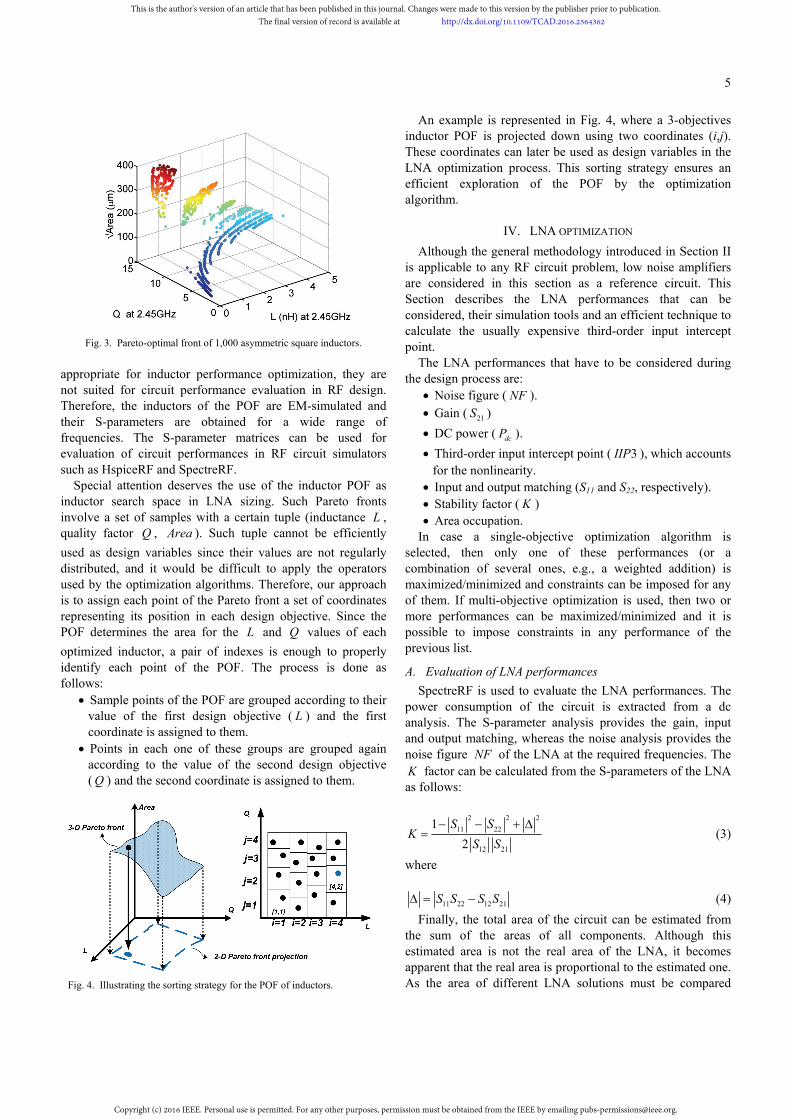
The inductor POF in Fig. 3 was generated for a 0.35-m CMOS technology, and contains 1000 asymmetric spiral square inductors intended to operate at 2.45GHz. The generation of this front takes approximately 7 days (wall clock time) in a computer with 2 CPU Intel(R) Xeon(R) E5-2630 v2 @ 2.60GHz with 12 cores. However, it has to be considered that this is a one-time investment, it can be generated much before it is needed as it does not require any information on the RF circuit topology in which it will be inserted or the circuit performance specifications.
The inductor POF shows the best trade-offs among L , Q
and Area. However, although these performances are
TABLE I DESIGN VARIABLES FOR INDUCTOR POF GENERATION
Parameter Minimum Maximum
N 1 10
W 5 μm 100 μm
Din 10 μm 390 μm
s 2.5 μm 2.5 μm
This is the author's version of an article that has been published in this journal. Changes were made to this version by the publisher prior to publication.The final version of record is available at http://dx.doi.org/10.1109/TCAD.2016.2564362
Copyright (c) 2016 IEEE. Personal use is permitted. For any other purposes, permission must be obtained from the IEEE by emailing [email protected].
5
appropriate for inductor performance optimization, they are not suited for circuit performance evaluation in RF design. Therefore, the inductors of the POF are EM-simulated and their S-parameters are obtained for a wide range of frequencies. The S-parameter matrices can be used for evaluation of circuit performances in RF circuit simulators such as HspiceRF and SpectreRF.
Special attention deserves the use of the inductor POF as inductor search space in LNA sizing. Such Pareto fronts involve a set of samples with a certain tuple (inductance L , quality factor Q , Area ). Such tuple cannot be efficiently
used as design variables since their values are not regularly distributed, and it would be difficult to apply the operators used by the optimization algorithms. Therefore, our approach is to assign each point of the Pareto front a set of coordinates representing its position in each design objective. Since the POF determines the area for the L and Q values of each
optimized inductor, a pair of indexes is enough to properly identify each point of the POF. The process is done as follows:
Sample points of the POF are grouped according to their value of the first design objective ( L ) and the first coordinate is assigned to them.
Points in each one of these groups are grouped again according to the value of the second design objective ( Q ) and the second coordinate is assigned to them.
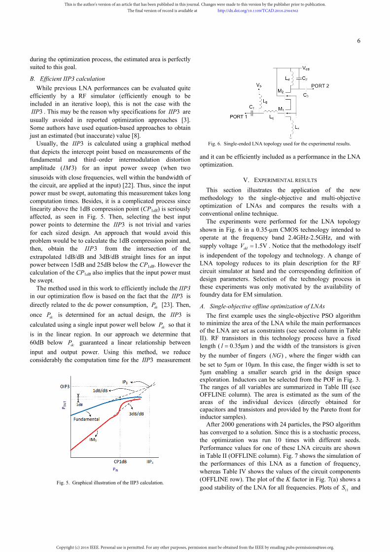
An example is represented in Fig. 4, where a 3-objectives inductor POF is projected down using two coordinates (i,j). These coordinates can later be used as design variables in the LNA optimization process. This sorting strategy ensures an efficient exploration of the POF by the optimization algorithm.
IV. LNA OPTIMIZATION
Although the general methodology introduced in Section II is applicable to any RF circuit problem, low noise amplifiers are considered in this section as a reference circuit. This Section describes the LNA performances that can be considered, their simulation tools and an efficient technique to calculate the usually expensive third-order input intercept point.
The LNA performances that have to be considered during the design process are:
Noise figure ( NF ). Gain ( 21S )
DC power ( dcP ).
Third-order input intercept point ( 3IIP ), which accounts for the nonlinearity.
Input and output matching (S11 and S22, respectively). Stability factor ( K ) Area occupation.
In case a single-objective optimization algorithm is selected, then only one of these performances (or a combination of several ones, e.g., a weighted addition) is maximized/minimized and constraints can be imposed for any of them. If multi-objective optimization is used, then two or more performances can be maximized/minimized and it is possible to impose constraints in any performance of the previous list.
A. Evaluation of LNA performances
SpectreRF is used to evaluate the LNA performances. The power consumption of the circuit is extracted from a dc analysis. The S-parameter analysis provides the gain, input and output matching, whereas the noise analysis provides the noise figure NF of the LNA at the required frequencies. The K factor can be calculated from the S-parameters of the LNA as follows:
2 2 2
11 22
12 21
1
2
S SK
S S
(3)
where
11 22 12 21S S S S (4)
Finally, the total area of the circuit can be estimated from the sum of the areas of all components. Although this estimated area is not the real area of the LNA, it becomes apparent that the real area is proportional to the estimated one. As the area of different LNA solutions must be compared
Fig. 4. Illustrating the sorting strategy for the POF of inductors.
Fig. 3. Pareto-optimal front of 1,000 asymmetric square inductors.
This is the author's version of an article that has been published in this journal. Changes were made to this version by the publisher prior to publication.The final version of record is available at http://dx.doi.org/10.1109/TCAD.2016.2564362
Copyright (c) 2016 IEEE. Personal use is permitted. For any other purposes, permission must be obtained from the IEEE by emailing [email protected].
6
during the optimization process, the estimated area is perfectly suited to this goal.
B. Efficient IIP3 calculation
While previous LNA performances can be evaluated quite efficiently by a RF simulator (efficiently enough to be included in an iterative loop), this is not the case with the
3IIP . This may be the reason why specifications for 3IIP are usually avoided in reported optimization approaches [3]. Some authors have used equation-based approaches to obtain just an estimated (but inaccurate) value [8].
Usually, the 3IIP is calculated using a graphical method that depicts the intercept point based on measurements of the fundamental and third–order intermodulation distortion amplitude ( 3)IM for an input power sweep (when two
sinusoids with close frequencies, well within the bandwidth of the circuit, are applied at the input) [22]. Thus, since the input power must be swept, automating this measurement takes long computation times. Besides, it is a complicated process since linearity above the 1dB compression point (CP1dB) is seriously affected, as seen in Fig. 5. Then, selecting the best input power points to determine the 3IIP is not trivial and varies for each sized design. An approach that would avoid this problem would be to calculate the 1dB compression point and, then, obtain the 3IIP from the intersection of the extrapolated 1dB/dB and 3dB/dB straight lines for an input power between 15dB and 25dB below the CP1dB. However the calculation of the CP1dB also implies that the input power must be swept.
The method used in this work to efficiently include the IIP3 in our optimization flow is based on the fact that the 3IIP is directly related to the dc power consumption, dcP [23]. Then,
once dcP is determined for an actual design, the 3IIP is
calculated using a single input power well below dcP so that it
is in the linear region. In our approach we determine that 60dB below dcP guaranteed a linear relationship between
input and output power. Using this method, we reduce considerably the computation time for the 3IIP measurement
and it can be efficiently included as a performance in the LNA optimization.
V. EXPERIMENTAL RESULTS
This section illustrates the application of the new methodology to the single-objective and multi-objective optimization of LNAs and compares the results with a conventional online technique.
The experiments were performed for the LNA topology shown in Fig. 6 in a 0.35-m CMOS technology intended to operate at the frequency band 2.4GHz-2.5GHz, and with supply voltage 1.5VddV . Notice that the methodology itself
is independent of the topology and technology. A change of LNA topology reduces to its plain description for the RF circuit simulator at hand and the corresponding definition of design parameters. Selection of the technology process in these experiments was only motivated by the availability of foundry data for EM simulation.
A. Single-objective offline optimization of LNAs
The first example uses the single-objective PSO algorithm to minimize the area of the LNA while the main performances of the LNA are set as constraints (see second column in Table II). RF transistors in this technology process have a fixed length ( 0.35μml ) and the width of the transistors is given
by the number of fingers ( )NG , where the finger width can
be set to 5μm or 10μm. In this case, the finger width is set to 5μm enabling a smaller search grid in the design space exploration. Inductors can be selected from the POF in Fig. 3. The ranges of all variables are summarized in Table III (see OFFLINE column). The area is estimated as the sum of the areas of the individual devices (directly obtained for capacitors and transistors and provided by the Pareto front for inductor samples).
After 2000 generations with 24 particles, the PSO algorithm has converged to a solution. Since this is a stochastic process, the optimization was run 10 times with different seeds. Performance values for one of these LNA circuits are shown in Table II (OFFLINE column). Fig. 7 shows the simulation of the performances of this LNA as a function of frequency, whereas Table IV shows the values of the circuit components (OFFLINE row). The plot of the K factor in Fig. 7(a) shows a good stability of the LNA for all frequencies. Plots of 11S and
Fig. 5. Graphical illustration of the IIP3 calculation.
Fig. 6. Single-ended LNA topology used for the experimental results.
This is the author's version of an article that has been published in this journal. Changes were made to this version by the publisher prior to publication.The final version of record is available at http://dx.doi.org/10.1109/TCAD.2016.2564362
Copyright (c) 2016 IEEE. Personal use is permitted. For any other purposes, permission must be obtained from the IEEE by emailing [email protected].

7
22S guarantee a good input and output matching whereas the
plots of 21S and NF show a well-behaved gain and noise
figure around the frequencies of interest. As stated above, the optimization algorithm was run 10
times. In all cases, the optimization constraints were met whereas different final values of area were obtained, whose statistical analysis is shown in Table V (OFFLINE row).
The LNA optimization (without the inductor POF generation) takes an average of 1.09 hours of CPU time in the same computer used for the inductor POF generation (the CPU time figure includes the addition of the CPU time spent in different processor cores, hence, the wall clock time can be reduced according to the number of cores used). It is important to remember that a new optimization of an LNA for different specifications does not require the generation of a new POF for the inductors, therefore the time above (~1 hour) is the real time on a practical application of the methodology for another circuit or a new set of specs.
It is interesting to study the effect of the indexing mechanism introduced in Section III. The blue continuous lines in Fig. 8 represent the evolution of the objective (area of the LNA) of the best solution vs. the number of iterations along 10 executions of the PSO algorithm using the indexing mechanism in Section III to select the inductors from the Pareto front. The plots do not start at the same iteration number since the objective is not plotted if any constraint is violated. If 10 executions are performed with the same PSO algorithm but with a random indexing of the solutions of the inductor front, then no execution is able to get a feasible solution after 2000 iterations. If a more sophisticated indexing
is used, e.g. for each inductor all the remaining inductors are sorted according to their Euclidean distance, then, only one execution is able to find a feasible solution before 2000 iterations (shown in red discontinuous line in Fig. 8). Hence, the indexing strategy used for the inductors of the Pareto front shows clear advantages to alternative techniques.
B. Comparison to conventional single-objective online optimization of the LNA
The offline methodology applied above is now compared with a conventional online optimization method. The optimization conditions (objective, constraints, number of particles and generations) are the same as the experiment of the previous section and so are the design variables for capacitors and transistors. Two alternative design variable sets could be used for the inductors:
(a) L and Q values, or
(b) geometric design variables.
TABLE II PERFORMANCES OF LNA CIRCUITS OBTAINED IN SINGLE-OBJECTIVE
OPTIMIZATION
Performance Specifications ONLINE OFFLINE
S21 (dB10) > 17 17.12 17.1
S11 (dB10) < -10 -10.84 -16.42
S22 (dB10) < -10 -20.79 -21.24
NF (dB20) < 3.5 3.28 3.42
Pdc (mW) < 7.8 7.77 7.74
IIP3 (dBm) > -10 -5.53 -6.12
K > 1 10.34 9.36 Area (μm2) Minimize 1.25x10⁵ 5.50x10⁴
TABLE III
DESIGN VARIABLES FOR SINGLE OBJECTIVE OPTIMIZATION
Component ONLINE OFFLINE
M1, M2 1 < NG < 120 1 < NG < 120
C1, C2, C3 100fF < C < 5pF 100fF < C < 5pF
Ls, Lg, Lb, Ld 1< N <10
5μm < W < 100 μm 10 μm < Din < 390 μm
Indexes of Inductor POF
Vb 0.5V < Vb < 1.5V 0.5V < Vb < 1.5V
(a)
(b)
Fig. 7. (a) Performances of the LNA circuit obtained by offline single-objective optimization. b) IIP3 curves for this LNA.
This is the author's version of an article that has been published in this journal. Changes were made to this version by the publisher prior to publication.The final version of record is available at http://dx.doi.org/10.1109/TCAD.2016.2564362
Copyright (c) 2016 IEEE. Personal use is permitted. For any other purposes, permission must be obtained from the IEEE by emailing [email protected].

8
The former alternative has lower accuracy, area cannot be estimated and the inductors still have to be sized after the optimization process. Therefore, the number of turns, turn width and inner diameter are used as inductor design variables. The inductors are modeled by the -model whose elements are defined in terms of geometric variables as described in [24] [25]. The ranges of geometric variables for inductors were set as indicated in Table III (ONLINE column) and the same maximum area constraint was applied to the inductors.
As in the previous experiment, the optimization process was run 10 times with different seeds. In one occasion, PSO could not find an LNA design that fulfilled the constraints. The statistical analysis of the results obtained for the other runs are shown in Table V (ONLINE row).
The LNA performance values obtained for one of the successful nine executions are included in Table II (ONLINE column) whereas Table IV shows the values of the circuit components (ONLINE row). Fig. 9 shows 11S , 22S , NF and
K of this LNA as a function of frequency (solid line), whereas Fig. 10 shows its 3IIP graphical calculation. Both graphs illustrate that the LNA behaves as expected in all the
frequency range, fulfilling all constraints. The LNA designs obtained in the 9 executions fulfill all performance constraints. However, the occupied area in each one of those 9 cases is larger than the area of any of the LNA designs obtained using the offline methodology, as shown in Table V. The big area difference can be rooted to the fact that the conventional online methodology explores the complete
TABLE IV COMPONENTS VALUES FOR THE LNA CIRCUITS INCLUDED IN TABLE II (FOR BOTH OFFLINE AND ONLINE SINGLE-OBJECTIVE OPTIMIZATION).
WM1 WM2 Vb C1 C2 C3 Ls Lg Lb Ld
OFFLINE 600μm 445μm 729mV 1.59pF 105.9fF 481fF N = 1
Din=10μm W=5μm
N = 5 Din=23μm W=5.05μm
N = 3 Din=98μm W=7.75μm
N = 6 Din=53μm W=5.05μm
ONLINE 370μm 450μm 781mV 3.47pF 100.3fF 561.4fF N = 1
Din=10μm W=6.15μm
N = 6 Din=104μm
W=5μm
N = 9 Din=38μm W=5μm
N = 3 Din=180μm W=7.7μm
Fig. 9. Performances of the LNA circuit obtained with online single-
objective optimization in Table IV simulated with the -model parameter for inductors (solid lines) and EM-simulated inductors (dotted line).
Fig. 10. IIP3 curves of the LNA circuit obtained with online single-
objective optimization in Table IV simulated with the -model parameter for inductors.
TABLE V
STATISTICAL RESULTS OF LNA AREA OBTAINED IN DIFFERENT RUNS OF
SINGLE-OBJECTIVE OPTIMIZATION FOR BOTH OFFLINE AND ONLINE
METHODOLOGIES
Methodology Mean (μm2) Worst (μm2) Best (μm2)
OFFLINE 7.05x10⁴ 9.94x10⁴ 4.87x10⁴
ONLINE 1.33x10⁵ 1.91x10⁵ 1.10x10⁵
Fig. 8 Area results vs. number of iterations for 10 executions of three different indexing techniques.
This is the author's version of an article that has been published in this journal. Changes were made to this version by the publisher prior to publication.The final version of record is available at http://dx.doi.org/10.1109/TCAD.2016.2564362
Copyright (c) 2016 IEEE. Personal use is permitted. For any other purposes, permission must be obtained from the IEEE by emailing [email protected].

9
search space of inductors whereas the proposed offline methodology only uses area-optimized inductors for the selected L-Q tuples.
In order to provide a fair comparison with the offline methodology, the inductors selected for the previous LNA obtained with the online methodology are EM simulated and their S-parameter matrices are incorporated into the LNA netlist. Then, the LNA is simulated again and its performances calculated for a wide range of frequencies. In this way, LNA performances are calculated with the same accuracy than the offline methodology. The results are included in Fig. 9 (dotted lines). As it can be observed, the LNA no longer fulfills the constraints imposed for the input matching. 11S is clearly
degraded, with a value above the specified constraint around the operating frequency. Other performances of the LNA circuit are also affected, especially 22S , as can be observed in
Fig. 9, although they still fulfill constraints. If inductance and quality factor of the inductors at the operating frequency are compared, significant differences between the values provided by the -model and those provided by EM simulation appear, especially for inductors bL and gL in Fig. 6, hence, explaining
the larger deviations in the input matching. Therefore, this implies that a new design iteration is
required to improve the input matching. Moreover, the number of redesign iterations until specifications are fulfilled is unpredictable.
The same accurate EM simulation of the final results provided by the other runs of the optimization algorithm provides the statistical results shown in Table VI. Not only the resulting area is much larger than in the offline case, but none of the results of the 10 runs satisfy the performance constraints when accurate EM simulation is used for the inductors. Therefore, redesign iterations become mandatory.
On the other hand, optimization times are very similar, with a CPU time of 1.08 hours for a single optimization run. This example clearly demonstrates the benefits of the methodology, where the undesirable redesign iterations common in RF circuit design have been avoided, as well as much better optimization results in terms of area occupation for a similar computation time are obtained.
C. Multi-objective optimization
The offline methodology can also be used to explore the trade-offs between the performances of an LNA by using a multi-objective optimization algorithm. Indeed, the first step of the methodology, the inductor POF generation, does not have to be performed, but the POF in Fig. 3 is used again. The design variables for the multi-objective optimization
algorithm are the same as for the PSO algorithm in Section II.A and shown in Table III (OFFLINE column). We can define two or more objectives to be optimized, depending on the trade-offs to be explored, subject to the required design constraints. The result is a POF of LNA designs that meet specifications and whose objective performances provide the best trade-offs between them, enabling RF designers to know the price to pay for improving certain performance of the LNA.
The LNA Pareto fronts obtained with a population of 1000 individuals after 300 generations for three different trade-offs,
21 . . dcS vs Area vs P , 21 . . dcS vs NF vs P and . . dcNF vs Area vs P ,
are shown in Figs. 11, 12, and 13, respectively. The objectives and constraints for these experiments are shown in Table VII. In the three examples, the Pareto optimal fronts provide designers with fully-sized designs incorporating EM-simulated inductors, giving them the possibility to select the design that better suits their needs. They can also be used for hierarchical bottom-up design of RF subsystems.
TABLE VI STATISTICAL ANALYSIS OF THE PERFORMANCES OF LNA CIRCUITS OBTAINED
IN SINGLE-OBJECTIVE ONLINE OPTIMIZATION AFTER ACCURATE EM
SIMULATION OF INDUCTORS
Performance Specifications Mean Worst Best
S21 (dB10) > 17 16.28 12.26 17.32
S11 (dB10) < -10 -8,94 -6.76 -14.63
S22 (dB10) < -10 -20.87 -12.00 -29.33
NF (dB20) < 3.5 3.19 3.31 3.06
Pdc (mW) < 7.8 7.92 9.59 7.68
IIP3 (dBm) > -10 -4.58 -5.48 -0.98
K > 1 11.86 8.81 21.81
Fig. 11. LNA Pareto-optimal front 21
. . dc
S vs Area vs P .
This is the author's version of an article that has been published in this journal. Changes were made to this version by the publisher prior to publication.The final version of record is available at http://dx.doi.org/10.1109/TCAD.2016.2564362
Copyright (c) 2016 IEEE. Personal use is permitted. For any other purposes, permission must be obtained from the IEEE by emailing [email protected].

10
In order to compare the advantages of our approach with the online methodology using multi-objective algorithms, we perform the same experiment of Fig. 11 but using the -model for the inductors, as it was done in Section V.B for the single-objective optimization. Fig. 14 shows a comparison between both results. Similar to the result with PSO, it is observed that the LNAs designs obtained in offline optimization reach similar performances but smaller areas than the LNAs obtained with online optimization.
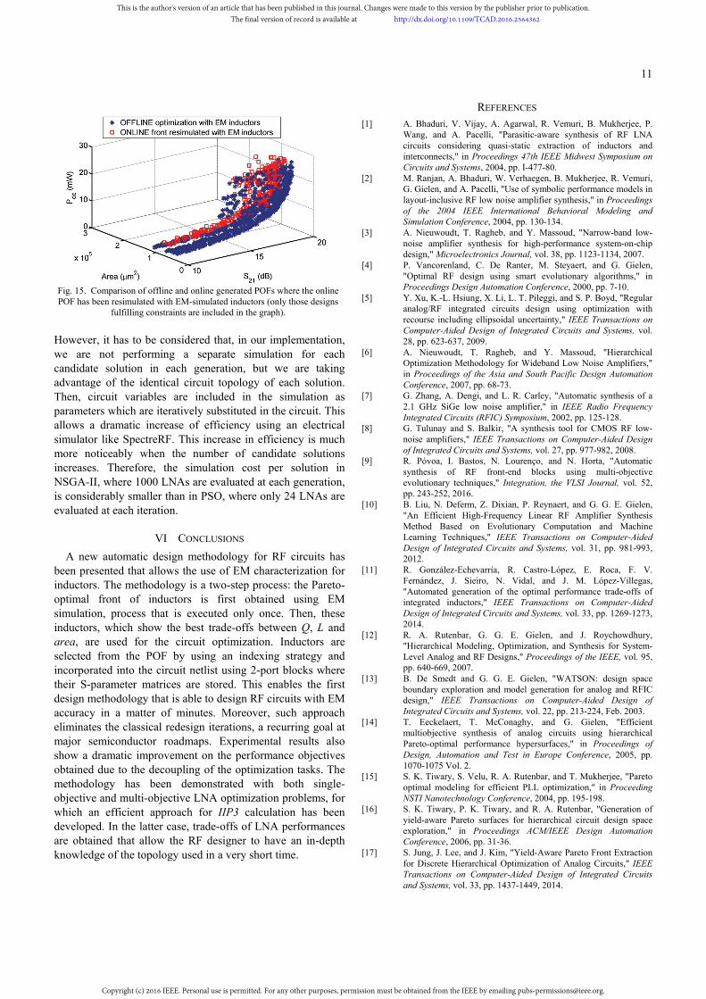
As it was done in Section V.B for the single-objective experiment, the inductors of all LNAs of the online POF of Fig. 14 are EM-simulated and the LNAs performances are therefore re-calculated with higher accuracy. Results are illustrated in Fig. 15. After re-simulation, 710 out of the initial 1000 LNA designs do not fulfill the design constraints initially imposed because their performance values have changed. This means that more than two thirds of the designs are useless. Table VIII summarizes these results, indicating the number of LNA designs that do not fulfill each constraint. Furthermore, if the coverage set metric [26] is applied between the offline POF in Fig. 11 and the re-simulated online POF in Fig. 15, results show that 100% of the designs of the online POF are dominated by designs obtained by the offline POF (this implies that for every point/design of the online POF there is at least one point/design of the offline POF with strictly better performances). These results clearly illustrate the advantage of using the offline methodology against conventional online methodologies.
On the other hand, the CPU time needed to generate the 1000 LNA designs of a Pareto-Optimal Front is 4.77 hours for the online case and 4.76 hours for the offline case in the same computer used for our previous experiments. It might seem surprising that the total CPU time is not much different from the single-objective optimization presented above, whereas the total number of simulations is much larger in NSGA-II (1,000 300 300,000 ) than in PSO ( 24 2,000 48,000 ).
TABLE VII
OBJECTIVES AND CONSTRAINTS FOR THE LNA TRADE-OFFS
Performance 21 . Area . dcS vs vs P 21 . . dcS vs NF vs P . . dcNF vs Area vs P
S21 (dB10) Maximize
> 10* Maximize
> 10* > 10
S11 (dB10) < -10 < -10 -
S22 (dB10) < -10 < -10 < -10
NF (dB 20) < 3.5dB Minimize Minimize
Pdc (mW) Minimize Minimize Minimize
IIP3 (dBm) > -10 > -10 > -10
K > 1 > 1 > 1 Area (μm2) Minimize - Minimize
* In this case, S21 is both an objective and a constraint.
TABLE VIII NUMBER OF LNA DESIGNS OF THE ONLINE EM-RESIMULATED POF THAT
DO NOT FULFILL CONSTRAINTS.
Performance Constraint Value No. of LNA Designs
ALL - 710
S21 (dB10) > 10 86
S11 (dB10) < -10 562
S22 (dB10) < -10 143
NF (dB 20) < 3.5dB 456
IIP3 (dBm) > -10 0
K > 1 0
Fig. 13. LNA Pareto-optimal front . .
dcNF vs Area vs P .
Fig. 14.
21. .
dcS vs Area vs P trade-off comparison: offline vs online
optimization. Fig. 12. LNA Pareto-optimal front
21 . .
dcS vs NF vs P .
This is the author's version of an article that has been published in this journal. Changes were made to this version by the publisher prior to publication.The final version of record is available at http://dx.doi.org/10.1109/TCAD.2016.2564362
Copyright (c) 2016 IEEE. Personal use is permitted. For any other purposes, permission must be obtained from the IEEE by emailing [email protected].
11
However, it has to be considered that, in our implementation, we are not performing a separate simulation for each candidate solution in each generation, but we are taking advantage of the identical circuit topology of each solution. Then, circuit variables are included in the simulation as parameters which are iteratively substituted in the circuit. This allows a dramatic increase of efficiency using an electrical simulator like SpectreRF. This increase in efficiency is much more noticeably when the number of candidate solutions increases. Therefore, the simulation cost per solution in NSGA-II, where 1000 LNAs are evaluated at each generation, is considerably smaller than in PSO, where only 24 LNAs are evaluated at each iteration.
VI CONCLUSIONS
A new automatic design methodology for RF circuits has been presented that allows the use of EM characterization for inductors. The methodology is a two-step process: the Pareto-optimal front of inductors is first obtained using EM simulation, process that is executed only once. Then, these inductors, which show the best trade-offs between Q, L and area, are used for the circuit optimization. Inductors are selected from the POF by using an indexing strategy and incorporated into the circuit netlist using 2-port blocks where their S-parameter matrices are stored. This enables the first design methodology that is able to design RF circuits with EM accuracy in a matter of minutes. Moreover, such approach eliminates the classical redesign iterations, a recurring goal at major semiconductor roadmaps. Experimental results also show a dramatic improvement on the performance objectives obtained due to the decoupling of the optimization tasks. The methodology has been demonstrated with both single-objective and multi-objective LNA optimization problems, for which an efficient approach for IIP3 calculation has been developed. In the latter case, trade-offs of LNA performances are obtained that allow the RF designer to have an in-depth knowledge of the topology used in a very short time.
REFERENCES [1] A. Bhaduri, V. Vijay, A. Agarwal, R. Vemuri, B. Mukherjee, P.
Wang, and A. Pacelli, "Parasitic-aware synthesis of RF LNA circuits considering quasi-static extraction of inductors and interconnects," in Proceedings 47th IEEE Midwest Symposium on Circuits and Systems, 2004, pp. I-477-80.
[2] M. Ranjan, A. Bhaduri, W. Verhaegen, B. Mukherjee, R. Vemuri, G. Gielen, and A. Pacelli, "Use of symbolic performance models in layout-inclusive RF low noise amplifier synthesis," in Proceedings of the 2004 IEEE International Behavioral Modeling and Simulation Conference, 2004, pp. 130-134.
[3] A. Nieuwoudt, T. Ragheb, and Y. Massoud, "Narrow-band low-noise amplifier synthesis for high-performance system-on-chip design," Microelectronics Journal, vol. 38, pp. 1123-1134, 2007.
[4] P. Vancorenland, C. De Ranter, M. Steyaert, and G. Gielen, "Optimal RF design using smart evolutionary algorithms," in Proceedings Design Automation Conference, 2000, pp. 7-10.
[5] Y. Xu, K.-L. Hsiung, X. Li, L. T. Pileggi, and S. P. Boyd, "Regular analog/RF integrated circuits design using optimization with recourse including ellipsoidal uncertainty," IEEE Transactions on Computer-Aided Design of Integrated Circuits and Systems, vol. 28, pp. 623-637, 2009.
[6] A. Nieuwoudt, T. Ragheb, and Y. Massoud, "Hierarchical Optimization Methodology for Wideband Low Noise Amplifiers," in Proceedings of the Asia and South Pacific Design Automation Conference, 2007, pp. 68-73.
[7] G. Zhang, A. Dengi, and L. R. Carley, "Automatic synthesis of a 2.1 GHz SiGe low noise amplifier," in IEEE Radio Frequency Integrated Circuits (RFIC) Symposium, 2002, pp. 125-128.
[8] G. Tulunay and S. Balkir, "A synthesis tool for CMOS RF low-noise amplifiers," IEEE Transactions on Computer-Aided Design of Integrated Circuits and Systems, vol. 27, pp. 977-982, 2008.
[9] R. Póvoa, I. Bastos, N. Lourenço, and N. Horta, "Automatic synthesis of RF front-end blocks using multi-objective evolutionary techniques," Integration, the VLSI Journal, vol. 52, pp. 243-252, 2016.
[10] B. Liu, N. Deferm, Z. Dixian, P. Reynaert, and G. G. E. Gielen, "An Efficient High-Frequency Linear RF Amplifier Synthesis Method Based on Evolutionary Computation and Machine Learning Techniques," IEEE Transactions on Computer-Aided Design of Integrated Circuits and Systems, vol. 31, pp. 981-993, 2012.
[11] R. González-Echevarría, R. Castro-López, E. Roca, F. V. Fernández, J. Sieiro, N. Vidal, and J. M. López-Villegas, "Automated generation of the optimal performance trade-offs of integrated inductors," IEEE Transactions on Computer-Aided Design of Integrated Circuits and Systems, vol. 33, pp. 1269-1273, 2014.
[12] R. A. Rutenbar, G. G. E. Gielen, and J. Roychowdhury, "Hierarchical Modeling, Optimization, and Synthesis for System-Level Analog and RF Designs," Proceedings of the IEEE, vol. 95, pp. 640-669, 2007.
[13] B. De Smedt and G. G. E. Gielen, "WATSON: design space boundary exploration and model generation for analog and RFIC design," IEEE Transactions on Computer-Aided Design of Integrated Circuits and Systems, vol. 22, pp. 213-224, Feb. 2003.
[14] T. Eeckelaert, T. McConaghy, and G. Gielen, "Efficient multiobjective synthesis of analog circuits using hierarchical Pareto-optimal performance hypersurfaces," in Proceedings of Design, Automation and Test in Europe Conference, 2005, pp. 1070-1075 Vol. 2.
[15] S. K. Tiwary, S. Velu, R. A. Rutenbar, and T. Mukherjee, "Pareto optimal modeling for efficient PLL optimization," in Proceeding NSTI Nanotechnology Conference, 2004, pp. 195-198.
[16] S. K. Tiwary, P. K. Tiwary, and R. A. Rutenbar, "Generation of yield-aware Pareto surfaces for hierarchical circuit design space exploration," in Proceedings ACM/IEEE Design Automation Conference, 2006, pp. 31-36.
[17] S. Jung, J. Lee, and J. Kim, "Yield-Aware Pareto Front Extraction for Discrete Hierarchical Optimization of Analog Circuits," IEEE Transactions on Computer-Aided Design of Integrated Circuits and Systems, vol. 33, pp. 1437-1449, 2014.
Fig. 15. Comparison of offline and online generated POFs where the online POF has been resimulated with EM-simulated inductors (only those designs
fulfilling constraints are included in the graph).
This is the author's version of an article that has been published in this journal. Changes were made to this version by the publisher prior to publication.The final version of record is available at http://dx.doi.org/10.1109/TCAD.2016.2564362
Copyright (c) 2016 IEEE. Personal use is permitted. For any other purposes, permission must be obtained from the IEEE by emailing [email protected].

12
[18] D. Mueller-Gritschneder and H. Graeb, "Computation of yield-optimized Pareto fronts for analog integrated circuit specifications," in Proc. Design, Automation & Test in Europe Conference & Exhibition (DATE), 2010, pp. 1088-1093.
[19] J. Kennedy and R. Eberhart, "Particle swarm optimization," in Proceeding IEEE International Conference on Neural Networks, 1995, pp. 1942-1948 (vol. 4).
[20] K. Deb, A. Pratap, S. Agarwal, and T. Meyarivan, "A fast and elitist multiobjective genetic algorithm: NSGA-II," IEEE Transactions on Evolutionary Computation, vol. 6, pp. 182-197, 2002.
[21] K. Deb, "An efficient constraint handling method for genetic algorithms," Computer Methods in Applied Mechanics and Engineering, vol. 186, pp. 311-338, 2000.
[22] T. H. Lee, The design of CMOS radio-frequency integrated circuits: Cambridge university press, 2004.
[23] Z. Heng and E. Sanchez-Sinencio, "Linearization techniques for CMOS low noise amplifiers: A tutorial," IEEE Transactions on Circuits and Systems I: Regular Papers, vol. 58, pp. 22-36, 2011.
[24] S. S. Mohan, M. D. M. Hershenson, S. P. Boyd, and T. H. Lee, "Simple accurate expressions for planar spiral inductances," IEEE Journal of Solid-State Circuits, vol. 34, pp. 1419-1424, Oct 1999.
[25] M. D. M. Hershenson, S. S. Mohan, S. P. Boyd, and T. H. Lee, "Optimization of inductor circuits via geometric programming," in Proceedings 36th Design Automation Conference, 1999, pp. 994-998.
[26] K. Deb, Multi-objective optimization using evolutionary algorithms. New York, NY, USA John Wiley & Sons, 2001.
This is the author's version of an article that has been published in this journal. Changes were made to this version by the publisher prior to publication.The final version of record is available at http://dx.doi.org/10.1109/TCAD.2016.2564362
Copyright (c) 2016 IEEE. Personal use is permitted. For any other purposes, permission must be obtained from the IEEE by emailing [email protected].

13
R. González-Echevarría received the engineering degree in telecommunications and electronics from the “Instituto Politécnico José Antonio Echevarría”, La Havana, Cuba, in 2007. He received the M.S degree in Microelectronics from the University of Seville, Seville, Spain, in 2011. Since 2010, he has been with the Institute of Microelectronics of Seville (IMSE-CNM, CSIC and University of Seville), where he is currently a PhD. student. His research interests lie in the field of integrated circuits, especially in
computer-aided design and design methodologies for analog and RF circuits.
E. Roca received the physics and the Ph.D. degrees from the University of Barcelona, Spain, in 1990 and 1995, respectively. From November 1990 to April 1995, she worked at IMEC, Leuven, Belgium, in the field of infrared detection aiming to obtain large arrays of CMOS compatible silicide Schottky diodes. Since 1995, she has been with the Institute of Microelectronics of Seville, (IMSE-CNM-CSIC), Spain, where she holds the position of Tenured Scientist. Her research interests lie in the field of modeling and design methodologies for analog,
mixed-signal and RF integrated circuits. She has been involved in several research projects with different institutions: Commission of the EU, ESA, ONR-NICOP, etc. She has also co-authored more than 70 papers in international journals, books, and conference proceedings.
R. Castro-López received the "Licenciado en Física Electrónica" degree (M.S. degree on Electronic Physics) and the "Doctor en Ciencias Físicas" (Ph.D. degree) from the University of Seville, Spain, in 1998 and 2005, respectively. Since 1998, he has been working at the Institute of Microelectronics of Seville (CSIC-IMSE-CNM) of the Spanish Microelectronics Center, where he now holds the position of Tenured Scientist. His research interests lie in the field of integrated circuits, especially
design and computer-aided design for analog and mixed-signal circuits. He has participated in several national and international R&D projects and co-authored more than 50 international scientific publications, including journals, conference papers, book chapters and the book Reuse-based Methodologies and tools in the Design of Analog and Mixed-Signal Integrated Circuits (Springer, 2006).
F.V. Fernández got the Physics-Electronics degree from the University of Seville, Spain, in 1988 and his Ph. D. degree in 1992. In 1993, he worked as a postdoctoral research fellow at Katholieke Universiteit Leuven (Belgium). From 1995 to 2009, he was an Associate Professor at the Dept. of Electronics and Electromagnetism of University of Seville, where he was promoted to full professor in 2009. He is also a researcher at IMSE-CNM (University of Seville and CSIC). His research interests lie in the design and design methodologies of analog, mixed-signal and radiofrequency
circuits. Dr. Fernández has authored or edited five books and has co-authored more than 100 papers in international journals and conferences. Dr. Fernández is currently the Editor-in-Chief of Integration, the VLSI Journal (Elsevier). He has served as General Chair of three international conferences and regularly serves at the Program Committee of several international conferences. He has also participated as researcher or main researcher in numerous national and international R&D projects
J. Sieiro received the PhD in Physics in 2001 from the University of Barcelona, Spain. From 2002 to 2003, he was a member of the ECTM group at the Delft University of Technology, Delft, The Netherlands, working in the modelling of passive components and in the design of RFIC circuits. Since 2003, he has been with the Department of Electronics at the University of Barcelona, where he is currently an Associate Professor. His research interests are in the modeling of passive components and RF circuits.
J.M. López-Villegas received the PhD degree in Physics from the University of Barcelona, Spain, in 1990. Currently he is the Director of the Group of Excellence for Radio Frequency Components and Systems, University of Barcelona, and Full Professor with the Electronic Department at the same University. His research interests include design optimization and test of RF systems and circuits performed using silicon and multilayered technologies, such as multichip modules and low
temperature co-fired ceramics, modeling and optimization of integrated inductors and transformers for RF-integrated circuit applications, particularly in the development of new homodyne transceiver architectures based on injection-locked oscillators, the use of 3-D simulators for electromagnetic analysis of RF devices, components, and systems, as well as the analysis of electromagnetic compatibility/electromagnetic interference problems, particularly the interaction of electromagnetic energy with biological tissues.
N. Vidal received the PhD degree in Physics from the University of Barcelona, Spain in 1995. Currently she is an Associate Professor with the University of Barcelona and is a member of the Group of Excellence for Radio Frequency Components and Systems, University of Barcelona. Her current research interests include use of time domain simulators to evaluate biological effects of electromagnetic energy, including antenna design and propagation related issues, and design for electromagnetic compatibility compliance of
electronic systems and circuits.
This is the author's version of an article that has been published in this journal. Changes were made to this version by the publisher prior to publication.The final version of record is available at http://dx.doi.org/10.1109/TCAD.2016.2564362
Copyright (c) 2016 IEEE. Personal use is permitted. For any other purposes, permission must be obtained from the IEEE by emailing [email protected].