an asynchronous system design and implementation...
TRANSCRIPT
AN ASYNCHRONOUS SYSTEM DESIGN AND
IMPLEMENTATION ON AN FPGA
A THESIS SUBMITTED TO THE GRADUATE SCHOOL OF NATURAL AND APPLIED SCIENCES
OF MIDDLE EAST TECHNICAL UNIVERSITY
BY
NİZAM AYYILDIZ
IN PARTIAL FULFILLMENT OF THE REQUIREMENTS FOR
THE DEGREE OF MASTER OF SCIENCE IN
ELECTRICAL AND ELECTRONICS ENGINEERING
SEPTEMBER 2006

Approval of the Graduate School of Natural and Applied Sciences
Prof. Dr. Canan ÖZGEN
Director
I certify that this thesis satisfies all the requirements as a thesis for the degree of Master of Science.
Prof. Dr. İsmet ERKMEN Head of Department
This is to certify that we have read this thesis and that in our opinion it is fully adequate, in scope and quality, as a thesis for the degree of Master of Science.
Prof. Dr. Hasan GÜRAN Supervisor Examining Committee Members Asst. Prof. Dr. Cüneyt BAZLAMAÇCI (METU,EE)
Prof. Dr. Hasan GÜRAN (METU,EE)
Asst. Prof. Dr. İlkay ULUSOY (METU,EE)
Dr. Şenan Ece SCHMIDT (METU,EE)
M.S. İbrahim Serdar TANER (ASELSAN )

iii
I hereby declare that all information in this document has been obtained and
presented in accordance with academic rules and ethical conduct. I also declare
that, as required by these rules and conduct, I have fully cited and referenced
all material and results that are not original to this work.
Nizam AYYILDIZ

iv
ABSTRACT
AN ASYNCHRONOUS SYSTEM DESIGN AND
IMPLEMENTATION ON AN FPGA
AYYILDIZ, Nizam
MS, Department of Electrical and Electronics Engineering
Supervisor : Prof. Dr. Hasan GÜRAN
September 2006, 109 pages Field Programmable Gate Arrays (FPGAs) are widely used in prototyping digital
circuits. However commercial FPGAs are not very suitable for asynchronous design.
Both the architecture of the FPGAs and the synthesis tools are mostly tailored to
synchronous design. Therefore potential advantages of the asynchronous circuits
could not be observed when they are implemented on commercial FPGAs. This is
shown by designing an asynchronous arithmetic logic unit (ALU), implemented in
the style of micropipelines, on the Xilinx Virtex XCV300 FPGA family. The hazard
characteristics of the target FPGA have been analyzed and a methodology for self-
timed asynchronous circuits has been proposed. The design methodology proposes
first designing a hazard-free cell set, and then using relationally placed macros
(RPMs) to keep the hazard-free behavior, and incremental design technique to
combine modules in upper levels without disturbing their timing characteristics. The
performance of the asynchronous ALU has been evaluated in terms of the logic slices
occupied in the FPGA and data latencies, and a comparison is made with a
synchronous ALU designed on the same FPGA.
Keywords: Asynchronous, self-timed, micropipeline, FPGA, incremental design
v
ÖZ
FPGA ÜZERİNDE BİR ASENKRON SİSTEM TASARIMI VE YAPIMI
AYYILDIZ, Nizam
Yüksek Lisans, Elektrik Elektronik Mühendisliği Bölümü
Tez Yöneticisi : Prof. Dr. Hasan GÜRAN
Eylül 2006, 109 sayfa
Alan programlamalı kapı dizinleri (FPGA) sayısal devre prototip tasarımlarında
yaygın olarak kullanılmaktadır. Ancak ticari FPGA’ler asenkron tasarım için çok
uygun değildir. FPGA’lerin mimari yapıları ve sentez araçları daha çok senkron
tasarımlara uygundur. Bu yüzden asenkron devrelerin potansiyel avantajları ticari
FPGA’ler üzerinde gerçekleştirildiklerinde görülememektedir. Bu çalışmada mikro
ardışık düzen tarzında gerçekleştirilmiş bir asenkron aritmetik ve mantık biriminin
(AMB) Xilinx Virtex XCV300 FPGA ailesi üzerinde tasarlanmasıyla gösterilmiştir.
Hedef FPGA’in zamanlama karakteristiği incelenmiş ve kendinden zamanlı asenkron
devre tasarımı için bir yöntem öne sürülmüştür. Yöntem, ilk olarak zaman-hasarsız
bir hücre kümesi tasarlamayı, daha sonra ilişkisel yerleşimli makrolar (RPM)
kullanarak zaman-hasarsız özellikleri korumayı, ve artımsal tasarım tekniğiyle
modüllerin üst seviyede zamanlama karakteristikleri kaybolmadan birleştirilmesini
ileri sürmektedir. Asenkron AMB’nin performansı FPGA içerisinde kapladığı mantık
parçaları ve veri gecikmesi bakımından değerlendirilmiş ve aynı FPGA üzerinde
gerçeklenen senkron bir AMB’yle karşılaştırılmıştır.
Anahtar Kelimeler: Asenkron, kendinden-zamanlı, mikro ardışık düzen, FPGA,
artımsal tasarım

vi
To my family, Cem Boran and Asya

vii
ACKNOWLEDGEMENTS
I would like to express my sincere gratitude to my advisor Prof. Dr. Hasan GÜRAN
for his guidance, advice, criticism, encouragements and insight throughout the
research.
I would like to express my special thanks and gratitude to Asst. Prof. Dr. Cüneyt
BAZLAMAÇCI, Asst. Prof. Dr. İlkay ULUSOY, Dr. Şenan Ece SCHMIDT and
M.S. İbrahim Serdar TANER for showing keen interest to the subject matter and
accepting to read and review the thesis.
I would like to thank ASELSAN Inc. for letting me involve in this thesis study and
for the facilities provided for the completion of this thesis.
I am grateful to my friends Erdinç ERÇİL, Can Barış TOP, Burak ALİŞAN, Bülent
ALICIOĞLU and Necip ŞAHAN for their help and morale support.
A very special gratitude goes to my family for their love and support throughout all
my life.
Finally, I would like to thank anybody that I might have mistakenly disregarded.

viii
TABLE OF CONTENTS
PLAGIARISM.......................................................................................................... iii
ABSTRACT.............................................................................................................. iv
ÖZ............................................................................................................................... v
ACKNOWLEDGEMENTS.................................................................................... vii
TABLE OF CONTENTS....................................................................................... viii
LIST OF FIGURES .................................................................................................. x
LIST OF TABLES .................................................................................................. xii
LIST OF ABBREVIATIONS ............................................................................... xiii
CHAPTERS
1. INTRODUCTION................................................................................................. 1
1.1. ASYNCHRONOUS DESIGN METHODOLOGIES....................................... 2
1.1.1. BOUNDED DELAY MODELS ................................................................ 2
1.1.2. DELAY-INSENSITIVE CIRCUITS ......................................................... 2
1.1.3. SPEED-INDEPENDENT AND QUASI-DELAY-INSENSITIVE
CIRCUITS ........................................................................................................... 3
1.1.4. MICROPIPELINES ................................................................................... 4
1.2. IMPLEMENTING ASYNCHRONOUS CIRCUITS USING FPGAS ............ 4
1.3. SCOPE OF THE THESIS................................................................................. 7
2. SELF-TIMED CIRCUITS ................................................................................... 8
2.1. CONTROL CIRCUITS FOR TRANSITION SIGNALING .......................... 10
2.2. EVENT-CONTROLLED STORAGE ELEMENT......................................... 11
2.3. CONSTRUCTION OF MICROPIPELINES .................................................. 12
3. FPGA IMPLEMENTATION............................................................................. 15
3.1. HAZARDS AND HAZARD ELIMINATION METHODS........................... 15
3.1.1. DEFINITIONS......................................................................................... 15
3.1.2. HAZARDS............................................................................................... 17
3.2. VIRTEX FPGA FAMILY ARCHITECTURE............................................... 20
3.2.1. HAZARD BEHAVIOR OF XILINX FPGAS ......................................... 23

ix
3.3. IMPLEMENTED HAZARD-FREE CELL SET ............................................ 25
3.3.1. MULLER-C ............................................................................................. 25
3.3.2. TOGGLE.................................................................................................. 26
3.3.3. SELECT ................................................................................................... 27
3.3.4. CALL ....................................................................................................... 29
3.3.5. OPAQUE LATCH ................................................................................... 30
3.4. FOUR-BIT ASYNCHRONOUS ALU ........................................................... 31
3.4.1. ONE-BIT REGISTER.............................................................................. 31
3.4.2. FOUR-BIT REGISTER ........................................................................... 32
3.4.3. FOUR-BIT AND...................................................................................... 34
3.4.4. FOUR-BIT OR......................................................................................... 35
3.4.5. FOUR-BIT COMPLEMENT................................................................... 36
3.4.6. PROGRAMMABLE DELAY ELEMENT (PDE) .................................. 37
3.4.7. LOADABLE SHIFT REGISTER............................................................ 38
3.4.8. MY_MODULE_HF ................................................................................. 43
3.4.9. ADDER/SUBTRACTER......................................................................... 45
3.4.10. MULTIPLIER........................................................................................ 47
3.4.11. DIVIDER ............................................................................................... 54
3.4.12. I/Os of ALU ........................................................................................... 61
3.5. INCREMENTAL DESIGN USING RELATIONALLY PLACED MACROS
................................................................................................................................ 62
3.5.1. RELATIONALLY PLACED MACROS (RPMS) .................................. 65
3.5.2. INCREMENTAL DESIGN FLOW......................................................... 66
4. NUMERICAL RESULTS .................................................................................. 68
5. HARDWARE IMPLEMENTATION ............................................................... 75
5.1. OPERATION MANUAL ............................................................................... 76
6. CONCLUSION.................................................................................................... 81
REFERENCES........................................................................................................ 83
APPENDICES
A. SIMULATION WAVEFORMS OF ASYNCHRONOUS MODULES ........... 88
B. CIRCUIT SCHEMATICS OF THE IMPLEMENTED PCB............................ 97
C. DESIGN FILES............................................................................................... 109
x
LIST OF FIGURES
Figure 2.1 Two-phase and four-phase handshakings .................................................. 8
Figure 2.2 Bundled Data Interface and Convention.................................................... 9
Figure 2.3 Latches Used as an Event Controlled Storage Register........................... 12
Figure 2.4 Control Circuit for a Micropipeline ......................................................... 13
Figure 2.5 Micropipeline without Processing ........................................................... 13
Figure 2.6 Micropipeline with Processing ................................................................ 14
Figure 3.1 Static hazards ........................................................................................... 17
Figure 3.2 Dynamic hazards ..................................................................................... 18
Figure 3.3 A flow table with essential hazard........................................................... 19
Figure 3.4 Virtex Architecture Overview ................................................................. 20
Figure 3.5 2-Slice Virtex CLB .................................................................................. 21
Figure 3.6 Detailed view of Virtex slice ................................................................... 22
Figure 3.7 LUT-Based Implementation .................................................................... 23
Figure 3.8 MULLER-C module and its truth function.............................................. 26
Figure 3.9 Black Box Representation of MULLER-C with Clear............................ 26
Figure 3.10 TOGGLE module and its truth function ................................................ 27
Figure 3.11 Black Box Representation of TOGGLE Module................................... 27
Figure 3.12 SELECT module and its truth function ................................................. 28
Figure 3.13 Black Box representation of SELECT Element .................................... 28
Figure 3.14 CALL module and its truth function...................................................... 29
Figure 3.15 Black Box Representation of CALL element ........................................ 29
Figure 3.16 OPAQUE LATCH module and its truth function ................................. 30
Figure 3.17 Black Box Representation of OPAQUE LATCH Element ................... 30
Figure 3.18 Circuit diagram of one-bit register ........................................................ 32
Figure 3.19 Black Box Representation of one-bit register........................................ 32
Figure 3.20 Circuit diagram of four-bit register........................................................ 33
Figure 3.21 Black Box Representation of four-bit register....................................... 33
Figure 3.22 Circuit Diagram of four-bit AND .......................................................... 34

xi
Figure 3.23 Black Box Representation of four-bit AND .......................................... 35
Figure 3.24 Circuit diagram of four-bit OR .............................................................. 35
Figure 3.25 Black Box Representation of four-bit OR ............................................. 36
Figure 3.26 Circuit Diagram of four-bit COMPLEMENT ....................................... 36
Figure 3.27 Black Box Representation of four-bit COMPLEMENT ....................... 37
Figure 3.28 Circuit diagram of PDE ......................................................................... 37
Figure 3.29 Black Box Representation of PDE......................................................... 38
Figure 3.30 Circuit diagram of loadable shift register (type 1) ................................40
Figure 3.31 Black Box Representations of loadable shift register (type 1) .............. 41
Figure 3.32 Circuit diagram of loadable shift register (type 2)…………………….42
Figure 3.33 Black Box Representation of loadable shift register (type 2)................ 43
Figure 3.34 Circuit diagram of my_module_hf ........................................................ 44
Figure 3.35 Black Box Representation of my_module_hf........................................ 45
Figure 3.36 Circuit diagram of ADD/SUB…………………………………………46
Figure 3.37 Black Box Representation of ADD/SUB module ................................. 47
Figure 3.38 Required Hardware for Signed-Magnitude Multiplication.................... 48
Figure 3.39 Hardware Flow Chart for Multiplication ............................................... 50
Figure 3.40 Circuit diagram of special modulo-4 counter ........................................ 51
Figure 3.41 Black Box Representation of special modulo-4 counter ....................... 52
Figure 3.42 4-bit Signed-Magnitude Multiplier…………………………………….53
Figure 3.43 Required Hardware for Signed-Magnitude Division............................. 55
Figure 3.44 Hardware Flow Chart for Signed-Magnitude Division ......................... 57
Figure 3.45 Four-bit Signed-Magnitude Divider…………………………………...60
Figure 3.46 Floorplanner view of the logic groups................................................... 67
Figure 5.1 Layout of the board (top view) ................................................................ 77
Figure 5.2 Top view of the board.............................................................................. 79

xii
LIST OF TABLES
Table 3.1 State transition table of my_module_hf .................................................... 44
Table 3.2 Input Decoding .......................................................................................... 61
Table 3.3 ALU Function Selection Opcode Decode Table....................................... 62
Table 3.4 Output Decoding ....................................................................................... 62
Table 4.1 Area and latency results of the self-timed modules .................................. 70
Table 4.2 Function latencies of asynchronous ALU (Top level implementation) .... 71
Table 4.3 Area and latency results of the synchronous modules .............................. 72
Table 4.4 Function latencies of synchronous ALU (Top level implementation) ...... 72
Table 5.1 Location references of the main integrated circuits of the PCB................ 78

xiii
LIST OF ABBREVIATIONS
ACK : Acknowledge
ALU : Arithmetic Logic Unit
ASIC : Application Specific Integrated Circuit
CLB : Configurable Logic Block
EDIF : Electronic Design Interchange Format
FPGA : Field Programmable Gate Array
IOB : Input/Output Block
LC : Logic Cell
LUT : Look-up Table
MIC : Multiple Input Change
PAR : Place and Route
PCB : Printed Circuit Board
REQ : Request
RPM : Relationally Placed Macro
SIC : Single Input Change
SOP : Sum of Products
STG : State Transition Graph
UCF : User Constraints File
VHDL : Very High Speed Integrated Circuit Hardware Description Language
VLSI : Very Large Scale Integrated Circuit
XST : Xilinx Synthesis Technology
1
CHAPTER 1
INTRODUCTION
The main points considered in digital circuit design are speed, the space occupied by
the circuit, the power consumption, reliability, adaptivity, modularity and finally the
cost. Circuit designers have searched for many years whether the synchronous or
asynchronous design methodology is more advantageous in fulfilling these
requirements.
Asynchronous circuits, in which the synchronization of the system components is
done without a global clock, can offer significant advantages over their synchronous
counterparts, which can be listed as elimination of clock skew problems, average
case performance instead of worst case performance, adaptivity to processing and
different environment variations, component modularity and reuse, lower system
power requirements, and reduced noise [1]. Main disadvantage of the asynchronous
circuits, however, is the design complexity. Eliminating hazards, critical races and
metastable states [2] in asynchronous circuits is a challenging task, especially in
large designs, and hence discourages the designers. The ease of synchronous design
attracts the designers also, since the time spent in design process is very crucial in
today’s industrial competition circumstances. As a result, asynchronous design is not
much preferred and the commercial devices and tools for circuit design and
simulation environments have been mostly tailored to synchronous circuits.
However, the potential advantages of the asynchronous circuits listed above have
always kept the interest of many researchers alive, who have been searching for an
alternative design technique.
2
1.1. ASYNCHRONOUS DESIGN METHODOLOGIES
Huffman and Muller are two pioneers who have established the base of the
asynchronous design methodologies in 1950s [1]. Huffman introduced a design
methodology, for what is known today as fundamental mode circuits [3], and Muller
developed the theoretical basics of the speed-independent circuits [4]. Any
asynchronous design methodology developed afterwards was inspired from one of
these two methodologies [1]. The study of Scott Hauck summarizes some of the more
notable asynchronous design methodologies [5].
1.1.1. BOUNDED DELAY MODELS
In Huffman’s methodology the circuits are designed under the bounded delay model,
that is, it is assumed that the delay in all circuit elements and wires is known [3]. The
circuits designed under this model are guaranteed to work regardless of the gate and
wire delays as long as the delay bound is known [1]. However, there are some
constraints to be met, which are; the input change is not allowed before the circuit
reaches stable state, and only single input change at a time is allowed [3].
The method, described by Hollaar [6] is an extension of Huffman circuits to non-
fundamental mode [5]. In that method the arrivals of new transitions are allowed to
be earlier than that allowed in fundamental mode assumptions.
Another design methodology, referred to as burst-mode was developed by Nowick,
Yun and Dill [7-10] allows multiple input changes as a burst in any order, but only
after the system has completely reacted to the previous input burst [5].
1.1.2. DELAY-INSENSITIVE CIRCUITS
Unlike the bounded-delay model, delay insensitive circuits are based on unbounded
gate delay model, that is, delays in both circuit elements and wires are assumed to be
unbounded [5]. In this model completion detection circuitry is required in order the

3
receiver to inform the sender that it has received the data properly, since there is no
guarantee that a wire will reach its proper value at any specific time due to
uncertainty in the delays, and hence a communication protocol (handshaking) is
established between data sender and receiver.
Martin has developed a design methodology for delay insensitive circuits with only
single-output gates [11], which is unsuitable for general circuit design [5].
A methodology, which makes delay insensitive circuit design practical for general
computations, has been proposed by Molnar et. al. [12]. This methodology is found
upon use of an I-Net, a model based on Petri Nets [13]. Via I-Net descriptions, delay
insensitive modules can be constructed, which eases the design of large systems
based on delay insensitivity concept. These modules are designed such that, all
timing constraints are encapsulated in them, hence the designer should not deal with
hazard problems during circuit construction.
The main power of module-based systems, however, is seen when they are coupled
with a high level language and automatic translation software, as described by
Brunvand and Sproull [14]. In this approach it is necessary to choose a language to
describe asynchronous circuits, and then provide delay-insensitive modules for each
of the language constructs.
Another methodology for delay-insensitive circuit design, based on trace theory, has
been proposed by Ebergen [15, 16], which uses a unified model for both module
specification and circuit design.
1.1.3. SPEED-INDEPENDENT AND QUASI-DELAY-INSENSITIVE CIRCUITS
As mentioned earlier speed-independent circuits are associated with D. E. Muller for
his pioneering work [4] on this model. This model assumes that while gate delays are
unbounded, all wire delays are negligible (less than the minimum gate delay) [5].
The quasi-delay insensitive circuits are a subclass of delay-insensitive circuits,

4
assuming both gate and wire delays are unbounded, augmenting this with isochronic
forks [17]. Isochronic wires are forking wires, where the delays between the branches
of this fork are negligible. The speed-independent and quasi-delay-insensitive
circuits are identical for all practical purposes [5].
Signal transition graphs (STGs) is a design methodology, introduced by Chu et. al.
[18, 19]. Like I-Nets, STGs specify asynchronous circuits with Petri-Nets [13] whose
transitions are labeled with signal names.
Change diagrams (CDs) [20] is another methodology similar to STGs, but avoid
some of the restrictions found in STGs.
The methodology, named as communicating process compilation technique [17],
developed by Martin, translates the program written in a language into asynchronous
circuits.
1.1.4. MICROPIPELINES
The micropipelines introduced by Sutherland offered an easy and simple way of
asynchronous design [21]. This work has brought to Sutherland the Turing Award,
and popularized the notion of a modular approach to control, focusing attention on
pipeline operations with transition signaling (2-phase handshaking). The
methodology explained in Sutherland’s study offers the opportunity of building up
complex systems by hierarchical composition of smaller and simpler pieces.
1.2. IMPLEMENTING ASYNCHRONOUS CIRCUITS USING FPGAS
With the improvement in VLSI technology, the designers have found the opportunity
to build faster, larger and more complex circuits. Field Programmable Gate Arrays
(FPGAs) offer an excellent alternative for rapid and inexpensive development of
these kinds of designs. While FPGAs can be directly used in the systems, they can

5
also be replaced by faster and smaller custom VLSI circuits (ASICs) after
prototyping has been completed.
While commercial FPGAs are utilized widely in synchronous designs, they are not
very suitable for asynchronous designs [22-25]. There are inconveniences for some
of the methodologies listed above in applying them in FPGAs. For example, the
speed-independent wire delay assumption is unrealistic in FPGAs, since wire delays
can often dominate logic delays. Also, the isochronic fork assumption, which is
easier to handle than speed independent wires, may not be handled in FPGAS, since
the equal delay between fork branches constraint may not be achieved due to
automatic routing. In bounded delay models, the feedback delays are very crucial,
but in FPGAs a feedback signal is routed like any other signal and it is difficult to
ensure that the feedback is fast enough for a changing element to stabilize before
another input arrives. Micropipelines are the most appropriate methodology among
the methodologies listed, since the implementation of micropipelines is very similar
to clocked systems. In micropipelines the control circuits take the place of global
clock for data synchronization. However the basic cell set proposed for control
circuits by Sutherland [21], is not directly available in conventional FPGAs, and their
design must be done first carefully. Also the delay between communicating modules
must be carefully handled for proper operation.
There are two types of approaches to utilize FPGAs in asynchronous circuit design.
The first one is developing specific circuit library in commercial FPGAs, and
constraining the place and route phase in order to avoid timing problems. And the
other one is offering a new type of FPGA architecture, which is suitable for
asynchronous design needs.
Brunvand has designed a library of circuit primitives for building self-timed (term
used for asynchronous circuits in which the synchronization is performed by
enforcing a simple communication protocol between circuit elements) circuits and
systems using Actel FPGAs [22]. The library modules use two-phase handshaking
protocol for control signals and bundled protocol for data signals. Brunvand and
Richardson have implemented the prototype of a comprehensive general purpose
6
processor, named as NSR (Non-synchronous RISC) [32], using Actel FPGAs,
assembling the two-phase transition control modules and bundled data modules of
the processor from that library. The deficiency of the study is that, hazard behavior
of the library modules has not been characterized. Moreover Actel FPGAs are not
suitable for prototyping, since they cannot be re-programmed, once programmed,
since they are based on anti-fuse architecture.
Maheswaran, in his MS. thesis study, implemented a hazard-free cell set for self-
timed circuits, based on the macromodules outlined in [21], in LUT (Look Up Table)
based Xilinx FPGAs [23]. He showed that, circuits designed using LUTs are logic-
hazard free, but could produce function- hazards for multiple-input changes. He also
formulated a set of feedback delay constraints for each of the self-timed elements
that are necessary to achieve hazard-free behavior. These constraints must be met
when placing and routing these modules for proper operation. Maheswaran also
proposed a new FPGA architecture, naming PGA-STG (Programmable Gate Array
for Implementing Self-Timed Circuits), which involves a logic block architecture
that is capable of satisfying all of the asynchronous necessities. The synthesis tool
corresponding to this architecture has been given in this study as well.
Moore and Robinson have proposed a solution for equipotential regions and
isochronic forks by combining floor and geometry planning tools [24]. With
constraining relative placement of the latches in the module to be designed, they
have achieved more predictable routing. They also have tackled the design of a
reliable arbiter, which is essential for many self-timed systems, by using the
technique they have developed. However, commercial floor planning tools are not
sufficient to avoid hazards, and automatic timing-driven FPGA implementation
cannot ensure hazard-free logic, although timing constraints are well described [25].
Ho et. al. developed a methodology presenting an alternative to enforce the mapping
in FPGAs to avoid hazard [25]. They developed a technique based on the use and
design of Muller gate library. Their approach is a combination of using standard
FPGAs and the TAST (TIMA Asynchronous Synthesis Tool) [26] developed at
TIMA (Techniques of Informatics and Microelectronics for Computer Architecture).

7
Several FPGA families, like Xilinx X4000, Xilinx Virtex, Altera Flex and Altera
Apex have been targeted in this study. They implemented a quasi-delay-insensitive
dual rail adder automatically, to demonstrate the potential of the methodology they
developed.
The FPGA architectures dedicated to asynchronous circuits are MONTAGE [27],
PGA-STG [23], GALSA [28], STACC [29], PAPA [30] and finally the architecture,
that has not a special name, developed by Huot et. al.[31]. Unfortunately, none of
these architectures have reached the chance to be produced commercially, since the
synchronous design is still more popular for designers.
1.3. SCOPE OF THE THESIS
In this thesis, an alternative methodology for implementing self-timed circuits on
commercial FPGAs is introduced. The basic asynchronous macromodule set
described in Sutherland [21], Brunvand [22] and Maheswaran [23], is re-
implemented using Xilinx Virtex XCV300 [33] series FPGAs. An asynchronous
ALU (Arithmetic Logic Unit) is constructed using this cell set, in a hierarchical
design flow. It is showed how to keep the delay properties of individual modules,
when they are instantiated in upper modules. The design is tested under simulation
environment (Modelsim) and also a hardware realization is performed on a printed
circuit board designed for this purpose.
This thesis consists of six chapters. Chapter 2 gives the principles of the self-timed
design and micropipelines, which describe the operation of the circuits constructed in
this thesis. In chapter 3 the implementation of the modules is explained in a
hierarchical order (from bottom to top). The key points of the design methodology
are also given in this chapter. The performance of the implemented modules is
evaluated in chapter 4 according to speed and area criteria. A comparison between
the asynchronous modules and their synchronous counterparts, implemented in the
same FPGA family, is done as well. The details of the printed circuit board are given
in chapter 5. Finally in chapter 6 the thesis is concluded and it is discussed what can
be done as future work.
8
CHAPTER 2
SELF-TIMED CIRCUITS
Self-timed circuits are asynchronous circuits, in which the data synchronization is
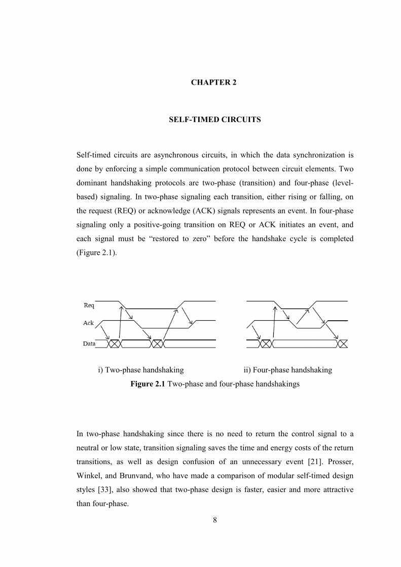
done by enforcing a simple communication protocol between circuit elements. Two
dominant handshaking protocols are two-phase (transition) and four-phase (level-
based) signaling. In two-phase signaling each transition, either rising or falling, on
the request (REQ) or acknowledge (ACK) signals represents an event. In four-phase
signaling only a positive-going transition on REQ or ACK initiates an event, and
each signal must be “restored to zero” before the handshake cycle is completed
(Figure 2.1).
i) Two-phase handshaking ii) Four-phase handshaking
Figure 2.1 Two-phase and four-phase handshakings
In two-phase handshaking since there is no need to return the control signal to a
neutral or low state, transition signaling saves the time and energy costs of the return
transitions, as well as design confusion of an unnecessary event [21]. Prosser,
Winkel, and Brunvand, who have made a comparison of modular self-timed design
styles [33], also showed that two-phase design is faster, easier and more attractive
than four-phase.
9
The coherence of control signals with data signals is also an important point in self-
timed circuit design. Data must be valid before the request is done. There are two
widely used protocols for data handling:
i) the dual-rail data convention, in which each data bit is represented by two signals;
ii) the bundled-data convention, in which each bit is represented by a single signal
and delays are inserted in the control paths to assure that data has settled before its
use (Figure 2.2).
In the dual-rail convention, a data bit is represented by one of the signal values 00
(meaning invalid data), 01 (bit is a valid 0), and 10 (bit is a valid 1). While this
convention has the advantage of providing a definite indication of the status of the
bit, its main disadvantage is doubling of the number of signal paths required for each
data bit.
In the bundled-data convention, the designer must determine worst-case estimates of
each data path for individual bits and groups of bits, and must insert appropriate
delays in the handshake control signals to assure that data is stable before a request is
asserted (the “bundling constraint”).
i) Bundled Data interface ii) Bundled Data Convention
Figure 2.2 Bundled Data Interface and Convention

10
The bundled data interface is easier to implement and takes less space when
compared to dual rail data interface [33].
2.1. CONTROL CIRCUITS FOR TRANSITION SIGNALING
The control circuits for transition signaling are built out of modules that form various
combinations of events. Here are the main control units taken from [21]:
XOR:
XOR provides the OR function for events. If any one of the inputs
changes states then the output also changes states, producing an
event.
MULLER-C:
When both inputs of the Muller-C are ‘0’ then the output is also ‘0’,
and when both inputs are ‘1’ the output is ‘1’, otherwise the output
remains same as previous value. Muller-C elements provide the
AND function for events. Assuming initially both inputs are at the
same state an event at the output only occurs when both inputs change.
TOGGLE:
TOGGLE steers events to its outputs alternately starting with
the dot. It is used mainly when one event is meaningful for two
different purposes, which should occur sequentially.
SELECT:
SELECT steers events according to the Boolean value of its
diamond input. It is used when a decision should be made, and
according to result different jobs are performed.
11
CALL:
CALL remembers which client, R1 or R2 called the procedure,
R, and after the procedure is done, D, returns a matching done
event on D1 or D2. The memory in the CALL element serves the
role of subroutine return address.
ARBITER:
ARBITER grants service G1 or G2, to only one input request, R1
or R2, at a time, delaying subsequent grants until after the
matching event done, D1 or D2.
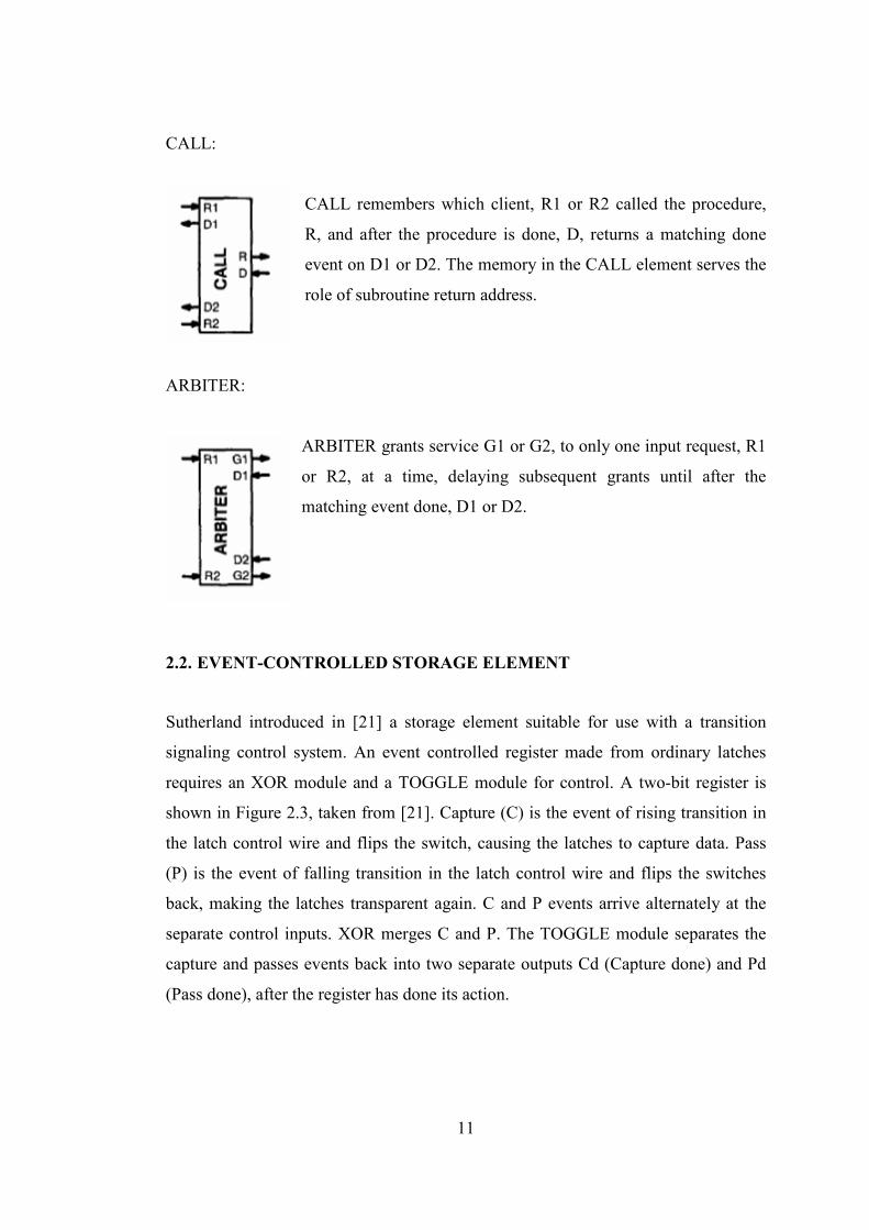
2.2. EVENT-CONTROLLED STORAGE ELEMENT
Sutherland introduced in [21] a storage element suitable for use with a transition
signaling control system. An event controlled register made from ordinary latches
requires an XOR module and a TOGGLE module for control. A two-bit register is
shown in Figure 2.3, taken from [21]. Capture (C) is the event of rising transition in
the latch control wire and flips the switch, causing the latches to capture data. Pass
(P) is the event of falling transition in the latch control wire and flips the switches
back, making the latches transparent again. C and P events arrive alternately at the
separate control inputs. XOR merges C and P. The TOGGLE module separates the
capture and passes events back into two separate outputs Cd (Capture done) and Pd
(Pass done), after the register has done its action.
12
Figure 2.3 Latches Used as an Event Controlled Storage Register
The implementations of the control circuits and storage element described here are
given in chapter 3.
2.3. CONSTRUCTION OF MICROPIPELINES
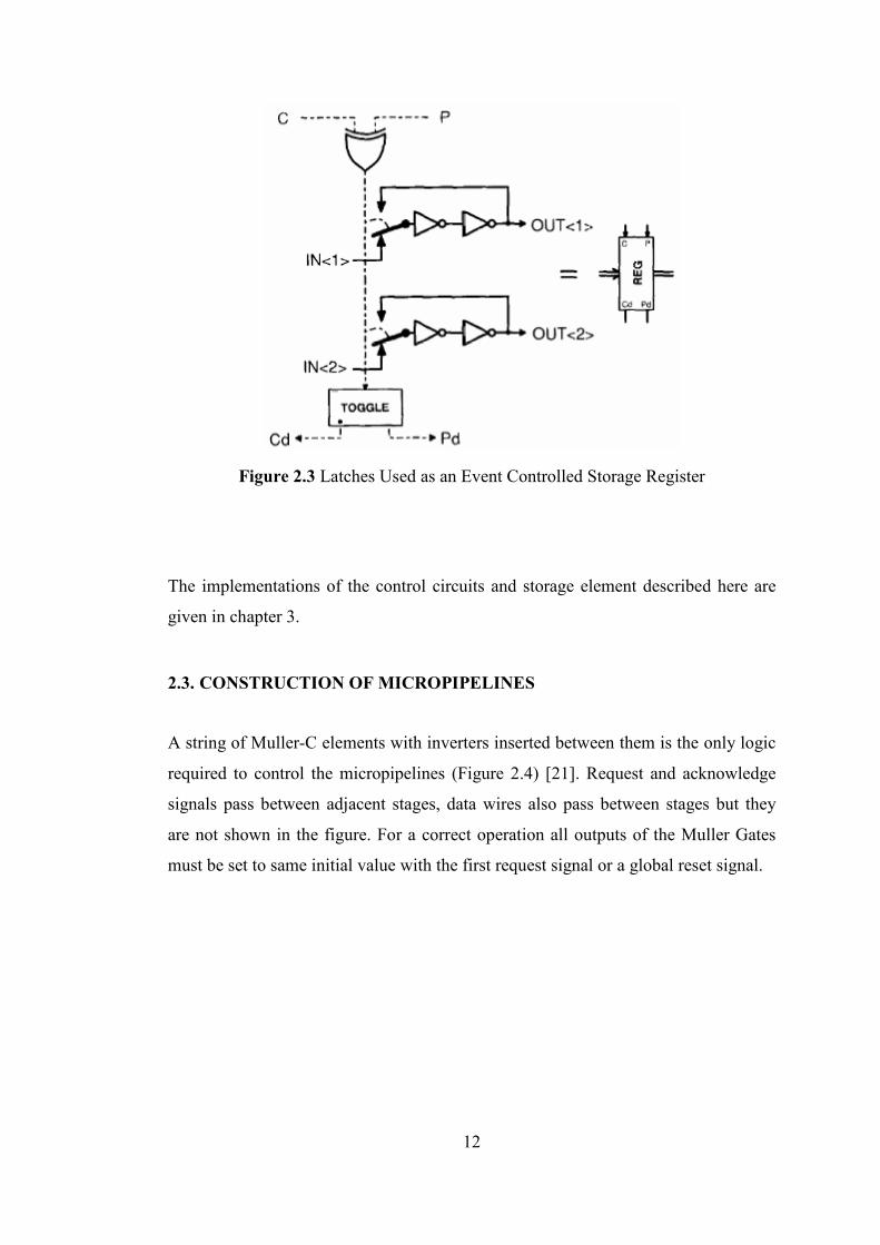
A string of Muller-C elements with inverters inserted between them is the only logic
required to control the micropipelines (Figure 2.4) [21]. Request and acknowledge
signals pass between adjacent stages, data wires also pass between stages but they
are not shown in the figure. For a correct operation all outputs of the Muller Gates
must be set to same initial value with the first request signal or a global reset signal.

13
Figure 2.4 Control Circuit for a Micropipeline
The simplest micropipeline structure can be seen in Figure 2.5. In this configuration
there is no processing and it is also simply a FIFO. The length of the FIFO can be
increased by adding more basic register blocks. If processing is needed, logic blocks
can be inserted between the register blocks (Figure 2.6). In this case the delays
between stages must be calculated according to the process time of the combinational
logic blocks between the registers.
Figure 2.5 Micropipeline without Processing

14
Figure 2.6 Micropipeline with Processing
15
CHAPTER 3
FPGA IMPLEMENTATION
An asynchronous system must be hazard-free for proper operation. Hazard-free
asynchronous circuits are assured by implementing them using a hazard-free cell set,
which are used according to constraints they enforce on the environment [16, 21, 22,
23, 25]. The design environment in this thesis is Xilinx XCV300 series FPGA which
is a member of Xilinx Virtex FPGA family [34].
This chapter consists of 5 sections. Section 3.1 gives a brief background on hazards
and hazard elimination techniques. In section 3.2 the characteristics of the target
FPGA family are given and it discusses the constraints under which the cell set
implemented on this FPGA will be hazard-free. In section 3.3 the basic cell set
implemented is presented. In section 3.4 the design of a 4-bit ALU is explained,
which is implemented using this cell set. The problems encountered during design
process for keeping the hazard-free behavior on the whole system, and how they are
handled, are explained in section 3.5.
3.1. HAZARDS AND HAZARD ELIMINATION METHODS
3.1.1. DEFINITIONS
The following definitions are taken from [1].
An incompletely specified Boolean function f of n variables x1, x2, … xn is a
mapping: f: {0,1}n → {0,1,−}.
Each element m of {0,1}n is called a minterm.
16
The ON-set of f is the set of minterms which return 1.
The OFF-set of f is the set of minterms which return 0.
The don’t care (DC)-set of f is the set of minterms which return −.
A literal is either the variable, xi, or its complement xi′. The literal xi evaluates to 1 in
minterm m when m(i) = 1. The literal xi′ evaluates to 1 when m(i) = 0.
A product is a conjunction (AND) of literals. A product evaluates to 1 for a given
minterm if each literal evaluates to 1 in minterm, and the product is said to contain
the minterm.
A set of minterms which can be represented with a product is called a cube.
The transition cube is the smallest cube that contains both m1 and m2 where m1 and
m2 are start and end points of the transition. A transition cube is denoted [m1, m2].
A product Y contains another product X (i.e., X ⊆ Y) if the minterms contained in x
are a subset of those in Y.
An implicant of a function is a product that contains no minterms in the OFF-set of
the function.
A prime implicant is an implicant which is contained by no other implicant.
A cover of a function is a SOP which contains the entire ON-set and none of the
OFF-set.

17
3.1.2. HAZARDS
3.1.2.1. COMBINATIONAL HAZARDS
In combinational circuits, due to the relative delay values along various paths,
spurious pulses, often termed glitches, may occur after input changes and this
situation results in unwanted output waveforms. This behavior is called
combinational hazard in the design [2]. Combinational hazards are classified as
either static or dynamic; depending upon the output is specified to remain constant
after the input change.
A circuit has static-0 hazard between the adjacent minterms m1 and m2 that differ
only in xj iff f(m1)=f(m2)=0, there is a product term, pi in the circuit that includes xj
and xj′, and all other literals in pi have value in m1 and m2 [35] (Figure 3.1).
A circuit has static-1 hazard between the adjacent minterms m1 and m2 where
f(m1)=f(m2)=1 iff there is no product term that has the value 1 in both m1 and m2 [35]
(Figure 3.1).
(i) Static-0 hazard (ii) Static-1 hazard
Figure 3.1 Static hazards
A SOP realization of f (assuming no product terms with complementary literals) will
be free of all static logic hazards iff the realization contains all prime implicants of f.
[36].

18
A SOP circuit has a dynamic hazard between adjacent minterms m1 and m2 that
differ only in xj iff f(m1) ≠ f(m2), the circuit has a product term pi that contains xj and
xj′, and all other literals of pi have value 1 in m1 and m2 [35] (Figure 3.2).
Figure 3.2 Dynamic hazards
For a multiple-input change (MIC) case, a function f has function hazard during
transition from m1 to m2 if there exist an m3 and m4 such that:
1. m3 ≠ m1 and m4 ≠m2
2. m3 ∈ [m1, m2] and m4 ∈ [m3, m2]
3. f(m1) ≠ f(m3) and f(m4) ≠f(m2)
If f( m1) = f(m2), it is a static function hazard, and if f(m1) ≠ f(m2), it is a dynamic
function hazard.
If there is a hazard in the circuit, although it could be implemented without that
hazard (i.e., the hazard is not a function hazard), then it is the characteristic of the
logic design, and is referred to as logic hazard [2].
If a Boolean function, f, contains a function hazard for the input change m1 to m2, it
is impossible to construct a logic gate network realizing f such that the possibility of
a hazard pulse occurring for this transmission is eliminated [36].
19
However, the synthesis method for expended burst mode (XBM) machines,
developed by Yun and Dill [37], never produces a design with a transition that has a
function hazard.
3.1.2.2. SEQUENTIAL HAZARDS
The violation of the assumption that outputs and state variables stabilize before either
new inputs or fed-back state variables arrive at the input to the logic can result in a
sequential hazard. The presence of a sequential hazard depends on the timing of the
environment, circuit and feedback delays.
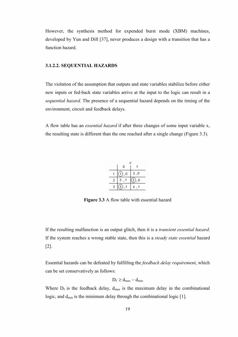
A flow table has an essential hazard if after three changes of some input variable x,
the resulting state is different than the one reached after a single change (Figure 3.3).
Figure 3.3 A flow table with essential hazard
If the resulting malfunction is an output glitch, then it is a transient essential hazard.
If the system reaches a wrong stable state, then this is a steady state essential hazard
[2].
Essential hazards can be defeated by fulfilling the feedback delay requirement, which
can be set conservatively as follows:
Df ≥ dmax − dmin
Where Df is the feedback delay, dmax is the maximum delay in the combinational
logic, and dmin is the minimum delay through the combinational logic [1].

20
Another timing problem in sequential circuits is critical races. A race condition
occurs when more than one state variables are excited simultaneously and the delays
associated with the excited state variables are different. The race is a critical race if
the state ultimately reached depends on the outcome of the race [2]. Critical races are
considered design defects, and they can always be eliminated by appropriate choices
of state assignments [2].
3.2. VIRTEX FPGA FAMILY ARCHITECTURE
Virtex devices feature a flexible, regular architecture that comprises an array of
configurable logic blocks (CLBs) surrounded by programmable input/output blocks
(IOBs), all interconnected by a rich hierarchy of fast versatile routing resources
(Figure 3.4).
Figure 3.4 Virtex Architecture Overview
CLBs, which provide the functional elements for constructing logic, interconnect
through a general routing matrix (GRM). The GRM comprises an array of routing
switches located at the intersections of horizontal and vertical routing channels.

21
The basic building block of the Virtex CLB is the logic cell (LC). A LC consists of a
4-input function generator, carry logic and a storage element. The output of the
function generator in each LC drives both CLB output and D input of the flip-flop.
Each Virtex CLB comprises 4 LCs, organized in two similar slices (Figure 3.5).
Figure 3.6 shows a more detailed view of a single slice.
Figure 3.5 2-Slice Virtex CLB
Virtex function generators are implemented as 4-input look-up tables (LUTs). An n-
input LUT-based implementation can be modeled as a combination of a memory of
2n depth, and an 2n : 1 multiplexer (Figure 3.7 shows 4-input LUT case as an
example). The content of the memory is the truth table of the function implemented,
and the memory content is fed to the data input of the multiplexer, which takes the
input of the functions as select inputs to it. Xilinx LUT architecture has a balanced
design with almost equal propagation delay from its inputs to its output.

22
F5 multiplexer in each slice combines the outputs of the function generators. This
combination provides either a function generator with 5 inputs, or a 4:1 multiplexer,
or selected functions up to 9 inputs. Similarly F6 multiplexer combines the outputs of
the F5 multiplexers in a CLB, hence all four outputs of the function generators. As a
result a function generator that accepts 6 inputs, or an 8:1 multiplexer or selected
functions up to 19 inputs can be implemented in a Virtex CLB.
Figure 3.6 Detailed view of Virtex slice

23
Figure 3.7 LUT-Based Implementation
3.2.1. HAZARD BEHAVIOR OF XILINX FPGAS
The hazard elimination methods, which are proposed for gate-level implementations,
are not valid for LUT-based implementations. This phenomenon has been
investigated comprehensively in Maheswaran’s thesis [23]. The following statements
are derived from that study.
If a function f has a function hazard during a transition [m1,m2] and if a set of
multiple input changes causes a transition from m1 to m2, then it may produce a
glitch at the LUT output. When more than one input changes simultaneously, the
presence of any intermediate code that produces a different result may cause a
decoding glitch. The glitch might be only a few nanoseconds long, but that is long
G1 G2 G3 G4 Z
0 0 0 0 D0
0 0 0 1 D1
0 0 1 0 D2
0 0 1 1 D3
0 1 0 0 D4
0 1 0 1 D5
0 1 1 0 D6
0 1 1 1 D7
1 0 0 0 D8
1 0 0 1 D9
1 0 1 0 D10
1 0 1 1 D11
1 1 0 0 D12
1 1 0 1 D13
1 1 1 0 D14
1 1 1 1 D15

24
enough to upset an asynchronous design, since the delays in the FPGA are pure, not
inertial. This can be avoided by using appropriate delay elements, but as there is no
user control over the delays inside of a function generator, function hazards cannot
be eliminated.
However, a function f is logic hazard-free for any transition for multiple input
changes when implemented using a Xilinx LUT. Logic hazards are defined in the
absence of function hazards, and therefore the transition should not consist of any
intermediate code that produces a different result. Since LUT produces output and
holds it steady during transition, the logic hazards are eliminated.
The LUT based asynchronous circuit implementations are essential hazard-free as
well. The essential hazards are caused by a change in the input reaching different
parts of the circuit at different times. These timing problems due to propagation
delays are possible in gate-level, but not in LUT-based implementations. In the case
of a LUT, a change in the input is detected by the function generator, which
implements the entire function at the same time and then the corresponding output is
selected from the configuration bits. Therefore, the new output is not fedback until
the entire circuit has detected the input change.
According to the findings above, it can safely be said and proven that all functions
implemented using a Xilinx LUT are hazard-free for single input changes as well.
The multiplexers in the CLB are also hazard-free, because the select inputs of the
multiplexers are hardwired when a function is mapped onto the CLB, which means
one of the inputs is transferred to the output, while the other one has no effect on the
output. In such a case there cannot be a transition that can produce any kind of
hazard.
Since CLB implements any combinational logic in a static, dynamic and essential
hazard-free manner, the only effect, which can still cause hazards to occur, is the
routing delay. All elements in the cell-set, except XOR, are sequential, and thus have
feedback. The feedback has to be available and stable, before new inputs arrive, in

25
order to preserve the hazard-free behavior. However the inputs are not changed until
the output is detected due to input/output mode of behavior, but can be changed
immediately after detection. Therefore the delay in the feedback line has to be less
than or equal to the sum of the minimal delay in detecting the output change and
producing a new input, and the minimal delay on the input line [23].
3.3. IMPLEMENTED HAZARD-FREE CELL SET
According to criteria described above, the basic asynchronous macromodule set
described in [21] has been implemented on Xilinx Virtex FPGA. The cell-set
includes MULLER-C, TOGGLE, SELECT, CALL, and OPAQUE LATCH. As
development environment ISE 6.3 (Xilinx Inc.), and as simulation tool Modelsim 5.7
SE (Mentor Graphics) have been utilized. The elements of the cell set have been
implemented with default properties of the ISE, the hazard-freeness of the elements
has been ensured according to the simulation results trying all possible input
configuration and transitions.
3.3.1. MULLER-C
Assuming both inputs (A and B) are at same logic level initially, a transition occurs
at the Q output only when both inputs change. When both inputs are ‘1’ then the
output is also ‘1’, and when both inputs are ‘0’ the output is ‘0’. In other cases the
output remains at previous state. The CLR input is added in order to make determine
the initial state of the output. The schematic and truth function can be seen in Figure
3.9. Black box representation of the module is shown also in Figure 3.9.
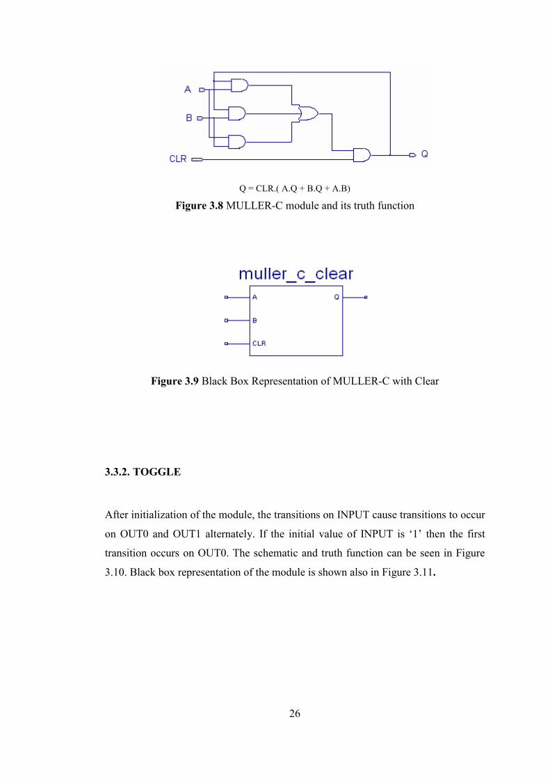
26
Q = CLR.( A.Q + B.Q + A.B)
Figure 3.8 MULLER-C module and its truth function
Figure 3.9 Black Box Representation of MULLER-C with Clear
3.3.2. TOGGLE
After initialization of the module, the transitions on INPUT cause transitions to occur
on OUT0 and OUT1 alternately. If the initial value of INPUT is ‘1’ then the first
transition occurs on OUT0. The schematic and truth function can be seen in Figure
3.10. Black box representation of the module is shown also in Figure 3.11.

27
OUT0 = CLR.(INPUT′.OUT0 + INPUT.OUT1′)
OUT1 = CLR.(INPUT′.OUT0 + INPUT.OUT1)
Figure 3.10 TOGGLE module and its truth function
Figure 3.11 Black Box Representation of TOGGLE Module
3.3.3. SELECT
According to SEL input, the transitions on EVENT_IN result in a transition on either
OUT_T or OUT_F. If SEL is ‘1’ then the transition occurs on OUT_T, and if SEL is
‘0’ the transition occurs on OUT_F. CLR input is used for initialization purposes.
The schematic and truth function can be seen in Figure 3.12. Black box
representation of the module is shown also in Figure 3.13.

28
OUT_F=CLR.(EVENT_IN′.OUT_T.OUT_F + EVENT_IN.OUT_F.OUT_T′ + SEL.OUT_F +
EVENT_IN.SEL′.OUT_T′)
OUT_T=CLR.(EVENT_IN′.OUT_T.OUT_F + OUT_T.SEL′ + OUT_F.SEL.EVENT_IN′ +
SEL.EVENT_IN.OUT_F′ + EVENT_IN.OUT_T.OUT_F′)
Figure 3.12 SELECT module and its truth function
Figure 3.13 Black Box representation of SELECT Element

29
3.3.4. CALL
CALL is used when there are two modules sharing one resource. It acts like a switch
between the client, who makes the request, and the shared resource. RS and AS are
request and acknowledge ports of the shared module, respectively. If there is an
event on R1 or R2 it is routed to RS, and the AS is routed back to A1 or A2, in
correspondence with which request has been done. The schematic and truth function
can be seen in Figure 3.14. Black box representation of the module is shown also in
Figure 3.15.
RS = R1 ⊕ R2
A1 = ((A1.(R2 ⊕ AS) + A1.R1 + R1.(R2 ⊕ AS))
A2 = ((A2.(R1 ⊕ AS) + A2.R2 + R2.(R1 ⊕ AS))
Figure 3.14 CALL module and its truth function
Figure 3.15 Black Box Representation of CALL element
30
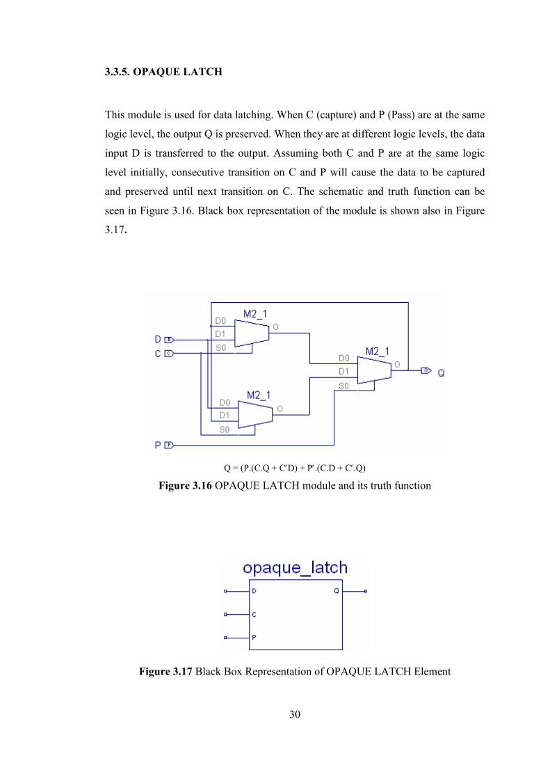
3.3.5. OPAQUE LATCH
This module is used for data latching. When C (capture) and P (Pass) are at the same
logic level, the output Q is preserved. When they are at different logic levels, the data
input D is transferred to the output. Assuming both C and P are at the same logic
level initially, consecutive transition on C and P will cause the data to be captured
and preserved until next transition on C. The schematic and truth function can be
seen in Figure 3.16. Black box representation of the module is shown also in Figure
3.17.
Q = (P.(C.Q + C′D) + P′.(C.D + C′.Q)
Figure 3.16 OPAQUE LATCH module and its truth function
Figure 3.17 Black Box Representation of OPAQUE LATCH Element

31
3.4. FOUR-BIT ASYNCHRONOUS ALU
A four-bit asynchronous ALU has been constructed, in order to demonstrate how
transition signaling and bundled data protocol are handled when designing a self-
timed system on an FPGA.
The ALU comprises the following units:
• 4-bit AND
• 4-bit OR
• 4-bit COMPLEMENT
• 4-bit LOADABLE SHIFT REGISTERS
• 4-bit ADDER/SUBTRACTOR
• 4-bit MULTIPLIER
• 8-bit by 4-bit DIVIDER
• additional logic for CONTROL purposes.
When implementing these units a hierarchical design flow has been followed. In the
following sections the modules designed in this thesis are explained in an order
somehow increasing complexity.
3.4.1. ONE-BIT REGISTER
It performs the function of event controlled storage element described in chapter 2.
When data is available at the input an event (transition) on C (capture) input causes
the latch to be transparent, i.e., the data passes to the output. The event, which occurs
on P (pass) after the transition on C, causes the data to be stored. The latch is closed
to new inputs until a transition occurs again on C. The acknowledgements of C and P
events are produced through a TOGGLE element. XOR element in front of the
TOGGLE transfers the transition on whichever of its inputs. Since the first transition
occurs always on C, the OUT0 output of the TOOGLE produces CD (capture done)
and the OUT1 output produces PD (pass done), which is the acknowledgement of
second transition. In the applications the CD output is directly connected to P input,
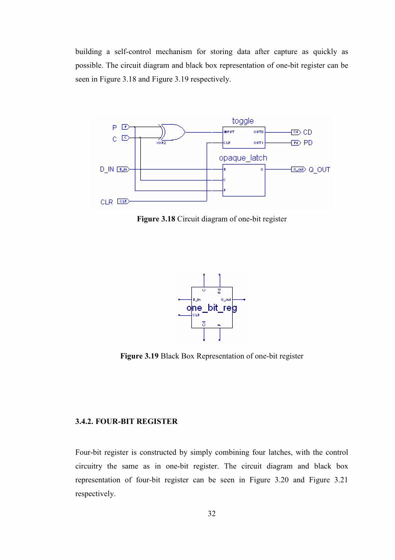
32
building a self-control mechanism for storing data after capture as quickly as
possible. The circuit diagram and black box representation of one-bit register can be
seen in Figure 3.18 and Figure 3.19 respectively.
Figure 3.18 Circuit diagram of one-bit register
Figure 3.19 Black Box Representation of one-bit register
3.4.2. FOUR-BIT REGISTER
Four-bit register is constructed by simply combining four latches, with the control
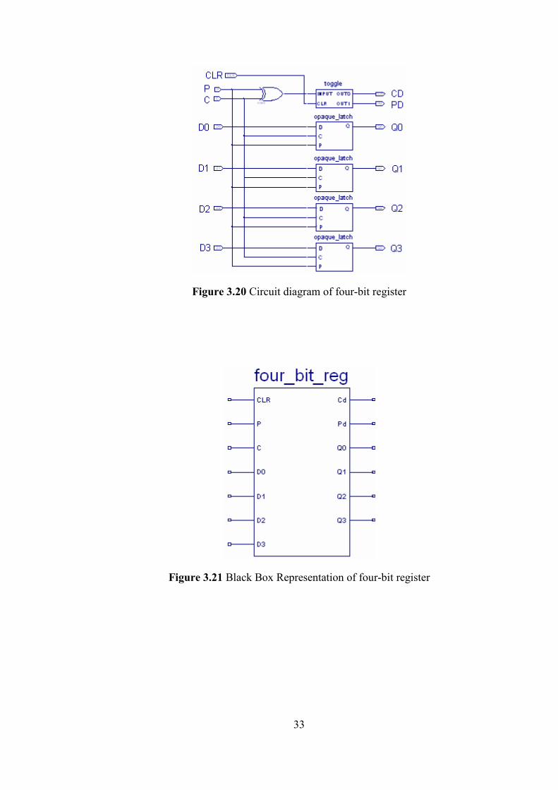
circuitry the same as in one-bit register. The circuit diagram and black box
representation of four-bit register can be seen in Figure 3.20 and Figure 3.21
respectively.
33
Figure 3.20 Circuit diagram of four-bit register
Figure 3.21 Black Box Representation of four-bit register

34
3.4.3. FOUR-BIT AND
This module performs logical AND of two four-bit inputs. The inputs are ANDed
combinational and the output of AND gates are registered using a four-bit register. A
transition on start input is the request for the module, after the data has been
available at the inputs. The start signal is connected to the capture (C) input of the
four-bit register. The acknowledge of the capture (Cd) is directly connected to the
pass (P) input of the register. Hence one transition is sufficient for both capturing
and passing the data. By the way there is no need to insert a delay element on the
request signal paths, since the transition on AND gates lasts less than the capture
acknowledgement generation. The final acknowledgement (Pd) indicates the end of
operation, and data is available at the output. The schematic and black box
representation of the four-bit AND is shown in Figure 3.22 and Figure 3.23
respectively.
Figure 3.22 Circuit Diagram of four-bit AND

35
Figure 3.23 Black Box Representation of four-bit AND
3.4.4. FOUR-BIT OR
This module is constructed similar to four-bit AND module except, OR gates are
used instead of AND gates. The schematic and black box representation of four-bit
OR is shown in Figure 3.24 and Figure 3.25 respectively.
Figure 3.24 Circuit diagram of four-bit OR

36
Figure 3.25 Black Box Representation of four-bit OR
3.4.5. FOUR-BIT COMPLEMENT
The concept of this module is not very different than AND and OR modules. The
four-bit input is inverted using NOT gates and then the output is registered. The
control signals are the same as those in AND and OR modules. The schematic and
black box representation of four-bit COMPLEMENT is shown in Figure 3.26 and
Figure 3.27 respectively.
Figure 3.26 Circuit Diagram of four-bit COMPLEMENT

37
Figure 3.27 Black Box Representation of four-bit COMPLEMENT
3.4.6. PROGRAMMABLE DELAY ELEMENT (PDE)
It is designed to use for delaying the control signal between processing units, in order
to implement bundled-data protocol. This module is simply serially connected
inverter chain. Each second inverter’s output is taken out of the module. There are
totally 16 inverters, hence 8 outputs, with an increasing delay. The programmability
comes from the selection option of one out of 8 different delayed versions of the
input signal. The circuit diagram and black box representation of PDE are as follows
shown in Figure 3.28 and Figure 3.29 respectively.
Figure 3.28 Circuit diagram of PDE

38
Figure 3.29 Black Box Representation of PDE
3.4.7. LOADABLE SHIFT REGISTER
The shift register is one of the basic modules of multiplier and divider. It is also used
stand alone as an ALU function. In this thesis two different shift register designs
have been implemented.
The first one is similar to conventional synchronous shift register. Four one bit
registers are connected serially, connecting the output and input of the neighboring
registers to each other. While the idea of the synchronous register is to apply a global
clock to all the registers and let the data progress in parallel, for an asynchronous
shift register, this is no longer the case since there is no such a global clock. The
registers cannot be triggered concurrently, since when they are made transparent to
data, there is no guarantee for only single bit transfer between them. Until they are
closed to data transfer with the second transition on their P input, there may occur
more than one data shift operations. The synchronization is achieved by making
neighboring stages communicate with each other. The rightmost register gets the
output of the register left of it and then acknowledges this operation; this is also a
request for the register left of it. The same procedure is repeated by all other
registers. Finally when the leftmost register acknowledges the transfer operation, the
shift process is done.
This shift register can also be loaded with a new data. Load operation has to be
differentiated from shift operation. However because of the serial connection of the
registers load operation is also achieved like a shift operation, with a difference; the
registers did not acquire the output of the previous register, but the load input,
sequentially. For the input differentiation of the registers for load and shift operation

39
a 2:1 multiplexer is put in front of each register. One input of the multiplexer is the
output of the previous register, and the other is the loadable bit. For the select input
of the multiplexers a specific module has been designed, which produces a “1”
output for load transitions, and a “0” output for shift operations (the design of this
module, named as my_module_hf, is described in the next section). The output of this
module is used as the select input of the multiplexer. Before shift or load operation
starts the inputs to the registers must be available. Therefore a delay element is put in
front of the first registers request input, so that the necessary time is given for the
settlements of both select input and hence the data. The acknowledgements of shift
and load operations are also differentiated, using a SELECT element. The select
input of this module is the same as the select input of the multiplexers, and the event
input is the acknowledgement signal of the last register. If the most significant bit
(MSB) of the input data is connected to the leftmost register, this is a shift right
register; and if the MSB of the input data is connected to the rightmost register, then
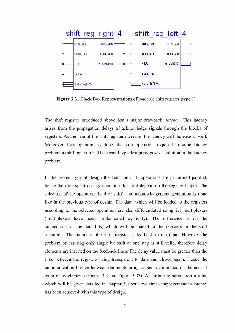
this is a shift left register. The schematic and black box representations of this type of
shift register are shown in Figure and Figure 3.31 respectively.

40
Figure 3.30 Circuit diagram of loadable shift register (type 1)
41
Figure 3.31 Black Box Representations of loadable shift register (type 1)
The shift register introduced above has a major drawback, latency. This latency
arises from the propagation delays of acknowledge signals through the blocks of
registers. As the size of the shift register increases the latency will increase as well.
Moreover, load operation is done like shift operation, exposed to same latency
problem as shift operation. The second type design proposes a solution to the latency
problem.
In the second type of design the load and shift operations are performed parallel,
hence the time spent on any operation does not depend on the register length. The
selection of the operation (load or shift), and acknowledgement generation is done
like in the previous type of design. The data, which will be loaded to the registers
according to the selected operation, are also differentiated using 2:1 multiplexers
(multiplexers have been implemented explicitly). The difference is on the
connections of the data bits, which will be loaded to the registers in the shift
operation. The output of the 4-bit register is fed-back to the input. However the
problem of assuring only single bit shift at one step is still valid, therefore delay
elements are inserted on the feedback lines. The delay value must be greater than the
time between the registers being transparent to data and closed again. Hence the
communication burden between the neighboring stages is eliminated on the cost of
extra delay elements (Figure 3.3 and Figure 3.33). According to simulation results,
which will be given detailed in chapter 5, about two times improvement in latency
has been achieved with this type of design.

42
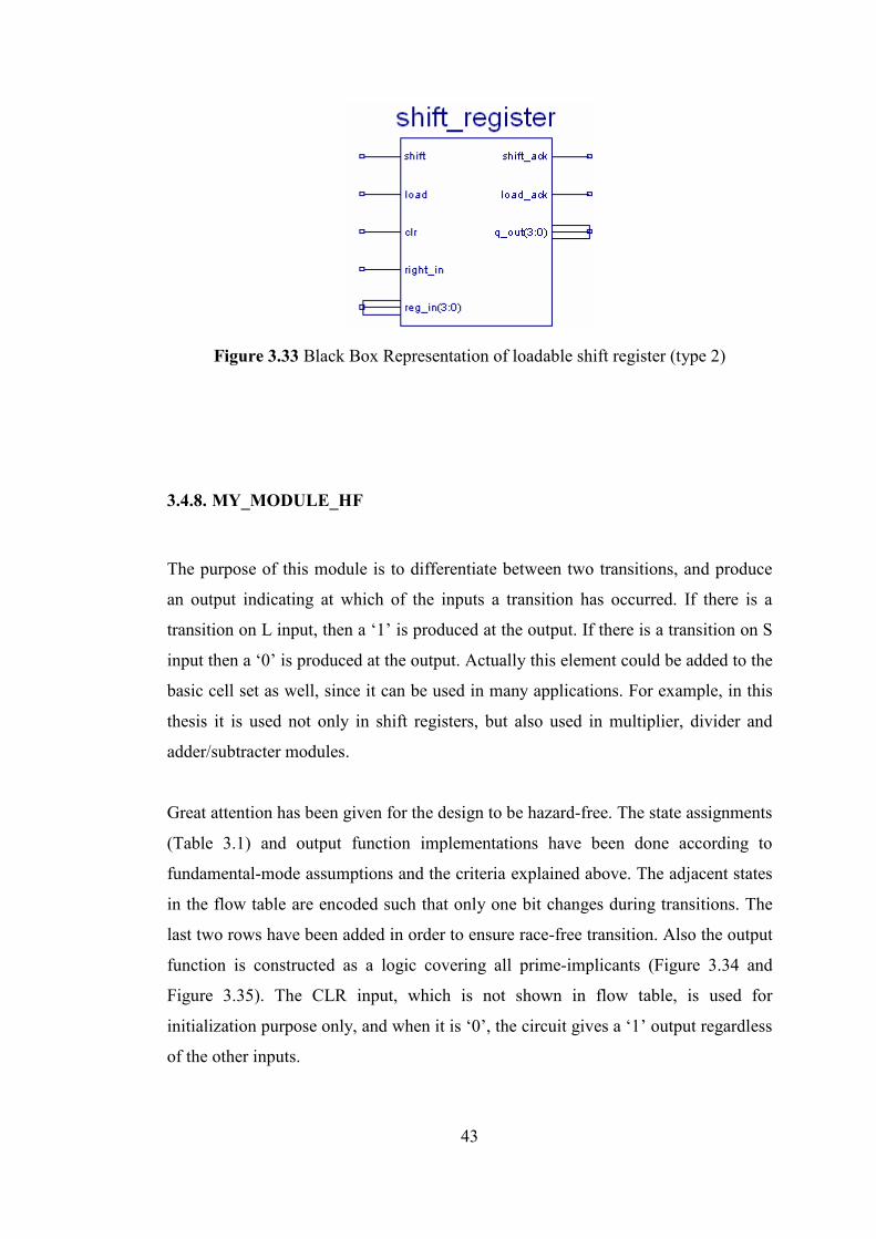
Figure 3.32 Circuit diagram of loadable shift register (type 2)
43
Figure 3.33 Black Box Representation of loadable shift register (type 2)
3.4.8. MY_MODULE_HF
The purpose of this module is to differentiate between two transitions, and produce
an output indicating at which of the inputs a transition has occurred. If there is a
transition on L input, then a ‘1’ is produced at the output. If there is a transition on S
input then a ‘0’ is produced at the output. Actually this element could be added to the
basic cell set as well, since it can be used in many applications. For example, in this
thesis it is used not only in shift registers, but also used in multiplier, divider and
adder/subtracter modules.
Great attention has been given for the design to be hazard-free. The state assignments
(Table 3.1) and output function implementations have been done according to
fundamental-mode assumptions and the criteria explained above. The adjacent states
in the flow table are encoded such that only one bit changes during transitions. The
last two rows have been added in order to ensure race-free transition. Also the output
function is constructed as a logic covering all prime-implicants (Figure 3.34 and
Figure 3.35). The CLR input, which is not shown in flow table, is used for
initialization purpose only, and when it is ‘0’, the circuit gives a ‘1’ output regardless
of the other inputs.

44
Table 3.1 State transition table of my_module_hf
PS: Present State NS:Next State
Figure 3.34 Circuit diagram of my_module_hf

45
Figure 3.35 Black Box Representation of my_module_hf
3.4.9. ADDER/SUBTRACTER
This module is used for addition and subtraction. For both operations it uses
basically a conventional adder. For addition, the operands are taken as they are and
carry-in of the adder is set to ‘0’. For subtraction 1’s complement of the second
operand (here minuend) is taken, and carry-in input is set to ‘1’, so subtrahend is
added with the 2’s complement of the minuend. Therefore for second input and
carry-in input of the adder multiplexers are used. The select inputs of these
multiplexers are produced by again my_module_hf modules like in the shift
registers. Similarly request signals are delayed, so that the necessary time is given for
the settlements of both select input and hence the data. The data input are registered
before addition/subtraction operation is performed, in order to eliminate false
outputs, which can be produced due to changes in the input data during
addition/subtraction process. The acknowledgements of the input registers are
ANDed via a MULLER-C element. The output of this MULLER-C element is used
as request input for the sum and carry-out registers. Again a delay element is inserted
between the MULLER-C output and register request inputs, in order to wait the sum
and carry-out outputs of the adder to be available. The value of the delay inserted has
to be greater than the process time of the adder, which is a combinational logic.
For two different request signals (add and sub) two different acknowledgement
signals (add_done, sub_done) are produced as well. This is accomplished by using a
SELECT module whose select input is the output of my_module_hf and event input

46
is the ANDed (via MULLER-C) acknowledgement signals of the output registers.
Figure 3.36 shows the schematic of the ADD/SUB module and Figure 3.37 shows
the black box representation of this module.
Figure 3.36 Circu
it diagram
of ADD/SUB
mod
ule

47
Figure 3.37 Black Box Representation of ADD/SUB module
3.4.10. MULTIPLIER
The multiplier designed in this thesis implements conventional shift and add
algorithm. This algorithm actually does what people are doing when they multiply
two binary numbers with paper and pencil. The conventional process can be
illustrated with a numerical example as follows.
The process consists of looking at successive bits of multiplier, least significant bit
(LSB) first. If the multiplier bit is a ‘1’, the multiplicand is copied down, and if ‘0’
zeros are copied down. The numbers copied down in successive lines are shifted one
position to the left from the previous number. Finally they are added, and their sum
gives the product.
In digital systems this algorithm is performed with a slight change. Instead of storing
all shifted multiplicands and adding them at the end of the operation, they are added
48
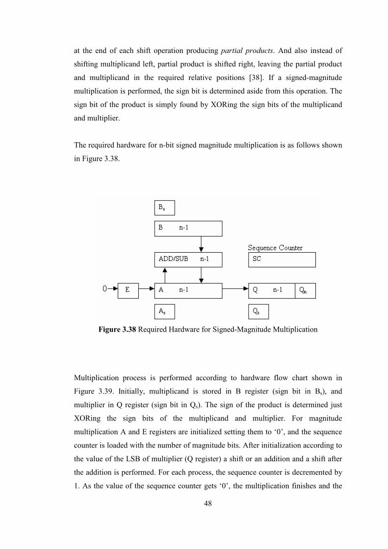
at the end of each shift operation producing partial products. And also instead of
shifting multiplicand left, partial product is shifted right, leaving the partial product
and multiplicand in the required relative positions [38]. If a signed-magnitude
multiplication is performed, the sign bit is determined aside from this operation. The
sign bit of the product is simply found by XORing the sign bits of the multiplicand
and multiplier.
The required hardware for n-bit signed magnitude multiplication is as follows shown
in Figure 3.38.
Figure 3.38 Required Hardware for Signed-Magnitude Multiplication
Multiplication process is performed according to hardware flow chart shown in
Figure 3.39. Initially, multiplicand is stored in B register (sign bit in Bs), and
multiplier in Q register (sign bit in Qs). The sign of the product is determined just
XORing the sign bits of the multiplicand and multiplier. For magnitude
multiplication A and E registers are initialized setting them to ‘0’, and the sequence
counter is loaded with the number of magnitude bits. After initialization according to
the value of the LSB of multiplier (Q register) a shift or an addition and a shift after
the addition is performed. For each process, the sequence counter is decremented by
1. As the value of the sequence counter gets ‘0’, the multiplication finishes and the
49
product is stored in A and Q registers, while most significant part resides in A, least
significant part resides in Q. The sign of the product is kept in As register.
The self-timed version of this architecture, implemented in this thesis as four-bit
signed-magnitude multiplier, consists of the following components:
• a four-bit register for multiplicand (B),
• two four-bit loadable shift registers for multiplier (Q) and partial product (A),
• four one-bit registers for sign bits (Bs, As and Qs) and for E,
• a four-bit adder (it has no infrastructure for subtraction, since there is no
need),
• a modulo-4 counter instead of a sequence counter (SC),
• two four-bit registers for registering the final content of A and Q registers
(the content of these registers are not visible at the output during the
multiplication process),
• basic cell-set elements and delay blocks for control and data handling.

50
Figure 3.39 Hardware Flow Chart for Multiplication
Multiplication begins with a transition on the start input. With this transition A, B,
Q, E, As and Bs registers are loaded with initial values. A and E registers are loaded
initially with ‘0’s, but during the multiplication process if an addition is performed,
A register is loaded with the sum output of the adder and E is loaded with the carry-
out output of the adder. Moreover E register must take a ‘0’ before a shift operation
is performed. Therefore the input data of A and E registers are selected according to
the process being performed. For this purpose multiplexers are utilized. The select
inputs of the multiplexers are generated by my_module_hf modules. So the initial
load request (start) and load requests after additions are differentiated from each
other. For E register also the shift operation is differentiated from load operations.
The requests which are wanted to be differentiated from each other, arrives both the

51
load or shift request input pins of the registers and L and S inputs of the
my_module_hf. The delay elements are inserted on the load request and shift request
paths of the registers, in order to wait for data to be available at the output of the
multiplexers before the requests reach the registers.
The number of shift and add operations is counted by a special modulo-4 counter
instead of a sequence counter. The modulo-4 counter (Figure 3.40 and Figure 3.41)
takes the transitions and steers every fourth transition to its mod_4 output while first,
second and third transitions are steered to mod_4_PRIME output. This module is
triggered after each shift operation. Since a shift occurs regardless of the value of the
LSB of Q register, the end of the operation can be determined by simply counting the
shift operations. So the shift acknowledge is connected to the input of modulo-4
counter. While the first three acknowledgements are directed to the module which
checks the LSB of Q register and determines accordingly whether a shift or addition
is done, the fourth transition is sent to the registers which will hold the final content
of As, A and Q registers as product output. When these registers acknowledge the
storage operation, by combining their acknowledge outputs to a MULLER-C element
a finish signal is generated to indicate the end of the operation and the product is
available at the output. The schematic design of 4-bit signed-magnitude multiplier
can be seen in Figure 3.42.
Figure 3.40 Circuit diagram of special modulo-4 counter
52
Figure 3.41 Black Box Representation of special modulo-4 counter

53
Figure 3.42 4-bit Signed-Magnitude Multiplier

54
3.4.11. DIVIDER
The divider designed in this thesis performs 4-bit signed-magnitude binary numbers
division. Like multiplier, the conventional algorithm, what people do when they
divide two binary numbers with paper and pencil, has been implemented. The
conventional algorithm is simply a process of successive compare, shift and subtract
operations. The division process is illustrated by a numerical example as follows:
For a 2n-bit dividend by n bit divisor case the process starts with comparing most
significant n bits of dividend with divisor. If divisor is greater, then a ‘0’ is put for
quotient and the divisor is shifted once to the right (this process can be thought as if
adding a ‘0’ in front of the MSB of divisor). Otherwise a ‘1’ is put for quotient and
the divisor is subtracted from the part of the dividend with which it is compared. The
divisor is shifted again after subtraction. The difference is called a partial remainder
[38] because the division could have stopped here to obtain a quotient of ‘1’ and a
remainder equal to the partial remainder. The process is continued by comparing
partial remainder with the divisor. If the partial remainder is greater than or equals
the divisor, the quotient bit is equal to ‘1’. The divisor is then shifted right and
subtracted from the partial remainder. If the partial remainder is smaller than the
divisor, the quotient bit is ‘0’ and no subtraction is needed. The divisor I shifted once
to the right in any case.
In digital systems this algorithm is performed with a slight change. Instead of
shifting the divisor to the right, the dividend or partial remainder is shifted to the left,
thus leaving the two numbers in the required relative positions. The hardware

55
required for division, and the hardware flow chart for signed-magnitude division can
be seen in Figure 3.43 and Figure 3.44 respectively.
Figure 3.43 Required Hardware for Signed-Magnitude Division
The dividend is contained in AsAQ and the divisor is contained in BsB. The sign of
the quotient (Qs) is determined by XORing the sign bits of the dividend and divisor.
If the sign bits are not counted, the dividend is of length 2n and divisor is of length n.
The register dedicated for quotient (Q) is also of length n. If the higher order half bits
of dividend constitute a number greater than or equal to divisor, then divide overflow
condition occurs. This means the quotient cannot be fit into n-bit register, it is at least
of length n+1. At the beginning of the operation this condition is checked, and if a
divide overflow condition exists, the process is exited by setting the DVF bit. If there
is no overflow condition the process is continued by magnitude division.
The division of magnitudes starts by shifting the dividend in AQ to the left with
high-order bit shifted into E. If the content of E is ‘1’, then it is obvious that EA > B,
since EA consists of a ‘1’ followed by n bits while B consists of only n bits. In this
case B is subtracted from A and a ‘1’ is inserted to Qn for quotient bit.

56
If the shift-left operation inserts a ‘0’ into E, then the contents of the A and B
registers are compared by subtracting B from A. The subtraction is done by adding
2’s complement of B to A. If the carry-out of the adder is ‘1’, it signifies that A ≥ B;
therefore a ‘1’ is inserted to Qn . If E is ‘0’ then it means that A < B, so in order to
restore original number B is added to A. There is no need to set Qn to ‘0’, since a ‘0’
is already inserted during the shift operation.
This process is repeated for n times. The flow control is done by assigning a
sequence counter initially to n and decrementing it by 1 after one shift, compare and
subtract cycle. When the content of this counter is ‘0’ then the operation is
completed, the remainder is in A, and the quotient is in Q.
57
Figure 3.44 Hardware Flow Chart for Signed-Magnitude Division

58
The self-timed version of this architecture, implemented in this thesis as four-bit
signed-magnitude divider, consists of the following components:
• a four-bit register for divisor (B),
• two four-bit loadable shift registers for dividend (Q and A),
• four one-bit registers for sign bits (Bs, As and Qs) and for E,
• a four-bit adder/subtracter ,
• a modulo-4 counter instead of a sequence counter (SC),
• two four-bit registers for registering the final content of A and Q registers
(the content of these registers are not visible at the output during the division
process),
• basic cell-set elements and delay blocks for control and data handling.
Division begins with a transition on the start input. With this transition A, B, Q, As
and Bs registers are loaded with initial values. A and Q registers are loaded initially
with dividend, but during the division process if an addition or subtraction is
performed, A register is loaded with the sum output of the add/sub block, and Q is
reloaded with its LSB set to ‘1’, if partial remainder is greater than or equals to
divisor. Therefore the input data of A and Q registers are selected according to the
process being performed. For this purpose multiplexers are utilized. The select inputs
of the multiplexers are generated by my_module_hf modules. So the initial load
request (start) and load requests after additions are differentiated from each other.
The requests which are wanted to be differentiated from each other, arrives both the
load or shift request input pins of the registers and L and S inputs of the
my_module_hf. The delay elements are inserted on the load request and shift request
paths of the registers, in order to wait for data to be available at the output of the
multiplexers before the requests reach the registers.
The number of shift-compare and subtract operations is counted by the same special
modulo-4 counter used in multiplier (Figure 3.40). This module is triggered after
each restore or set Qn to ‘1’ operation. Since one of these operations occurs at the
end of each comparison, the end of the operation can be determined by simply
counting the comparison operations. While the first three acknowledgements are

59
directed to initiate shift-left operation, the fourth transition is sent to the registers
which will hold the final content of A, Q and Qs registers as remainder and quotient
output. When these registers acknowledge the storage operation, by combining their
acknowledge outputs to a MULLER-C element a finish signal is generated to
indicate the end of the operation and the remainder and quotient are available at the
output. The schematic design of 4-bit signed-magnitude divider can be seen in Figure
3.45.

60
Figure 3.45 Four-bit Signed-Magnitude Divider
61
3.4.12. I/OS OF ALU
The individual functional units described above have been combined in a top
module. The top module takes two data input, one of them is of length 8 (REG1) and
the other is of length 4 (REG2). According to the function implemented the
meaningful bits differ. Table 3.2 shows which bits of REG1 and REG2 are
meaningful for which operation. Also for multiplication and division there are two
one-bit inputs (as and bs) that indicate the sign bits of operands. For other operations
they are don’t cares.
The top module has also CLR input, for initialization of the modules, and START as
the external REQUEST input of the ALU.
The function of the ALU is selected through an opcode. The opcode has 5 bits, and
the least significant three bits determine whether the ALU will perform AND, OR,
COMPLEMENT, ADD, SUBTRACT, MULTIPLY or DIVIDE operation, while the
most significant determines whether the output of the operation will be shifted left,
shifted right or kept as it is. Table 3.3 gives the opcode decoding.
The outputs of the functional units are decoded in eight-bit OUTREG output of the
ALU. The sign bits of product and division are also multiplexed with the carry-out
bits of adder/subtracter unit in qs output. The decoding of OUTREG and qs is shown
in Table 3.4. The ALU has also a DVF output dedicated for divide overflow
condition of divider and a FINISH signal as external ACKNOWLEDGE of the ALU.
Table 3.2 Input Decoding

62
Table 3.3 ALU Function Selection Opcode Decode Table
Table 3.4 Output Decoding
3.5. INCREMENTAL DESIGN USING RELATIONALLY PLACED MACROS
As mentioned before, the initial step for designing asynchronous systems is to obtain
a hazard-free cell set. Hazard-free circuits can be obtained by meeting firstly the
design constraints such as covering all prime implicands in the SOP implementation,
encoding adjacent states with adjacent code words etc., and secondly the timing
constraints such as feedback delay constraint, and bundled data constraints in self-
timed systems. While the design defects are independent of the environment on
which the system is constructed, and can be eliminated on paper before starting
implementation, the timing problems strongly depend on the design environment,
and are mostly handled during implementation stage. Actually eliminating timing
problems means adjusting delays properly.

63
In an FPGA the design can be entered in two different ways, using HDLs (Hardware
Description Languages) or schematic entry tool. Two widely used HDLs are Verilog
and VHDL (VHSIC HDL), where VHSIC stands for Very High Speed Integrated
Circuits. The synthesizers (XST, Examplar, Precision etc.) produce EDIF (Electronic
Design Interchange Format) files from the design entries. EDIF is a standard
interface-file specification. EDIF files are used by place-and-route (PAR) tools for
mapping the logic into the architectural resources of the FPGA (CLBs, IOBs etc.).
PAR tools then determine the locations for these blocks based on their
interconnections and finally interconnect the blocks.
The placement and delays depend very much on the performance of the tools used. In
this thesis, as mentioned before, Xilinx’s ISE (Integrated Software Environment) tool
has been utilized. ISE provides text and schematic editors for HDL and schematic
design entries; XST (Xilinx Synthesis Technology) as synthesizer, and PAR tools.
While PAR tools can implement the designs automatically, they allow the user view
and modify the placed design (via Floorplanner) as well as view and modify the
physical implementation, including routing (via FPGA Editor).
At the beginning, basic cell set elements have been entered in schematic editor, and
placement and routing has been made automatically. The hazard behavior of the units
has been checked by making simulations. In the simulations all possible input
combinations have been tried. If a hazard is observed, this is mainly a sequential
hazard, since there is no possibility for logic-hazards to occur in LUT-base
implementations (refer to section 3.2.1). The main reason for sequential hazards is
unfavorable routing. Automatic routing may not satisfy the feedback delay to be less
than or equal to the sum of the minimal delay in detecting the output change and
producing a new input, and the minimal delay on the input line. In this case the delay
constraints can be met either by making the routing by hand using FPGA editor, or
adding extra delay elements where the delay should be greater than others. In this
thesis the second approach has been preferred. The only element at which hazard has
been observed after automatic routing was the TOGGLE element. All of the other
basic cell set elements were hazard-free. TOGGLE element has also been
implemented as hazard-free after inserting two buffers on the data paths. An

64
important point which must be considered in buffer insertion is that, the nets before
and after the buffer must be associated with KEEP property set to TRUE, so that
synthesis tool does not remove the buffer when it optimizes the circuit, since during
optimization the synthesis tool appreciates the two nets before and after the buffer
equal and finds the buffer as an unnecessary gate between these nets.
After obtaining a complete hazard-free cell set, the next step was to implement self-
timed circuits using these elements. The timing problem, which must be handled in
the self-timed systems, is bundled-data constraint, i.e., the data must be available
before a request arrives to the processing unit. This constraint can be met by delaying
control signals for data process time. The control signals are delayed using PDE
elements, whose structure is described in section 4.6. PDE is a chain of inverters, and
similar to buffers if the nets between inverter gates are not associated with the KEEP
property set to TRUE they are removed by the synthesis tool.
During the design process of self-timed circuits, it has been seen that the basic cell
set elements could exhibit hazardous behavior, when they are instantiated in upper
level modules, although they were implemented as hazard-free individually. The
reason for this situation is that, when they are instantiated in upper blocks, their
placement and routing is different than the placement and routing as they were
implemented as single blocks. The random behavior of PAR tool also complicates
the adjusting delays for bundled data protocol. For each new delay value a new
placement is encountered. While a system can operate correctly for a delay value, it
may not operate for higher delay values. This is an unexpected case, since for correct
operation there is only a lower limit for delay and for delay values higher than the
lower limit the system should operate correctly. When increasing the delay the
remaining circuit does not keep its placement and routing, and hence the delay
assumptions made in one case may fail in another case. The unfavorable effect of
unpredictable routing can be decreased extensively, although not fully eliminated, by
creating relationally placed macros (RPM) of the design units, and using incremental
design techniques.
65
3.5.1. RELATIONALLY PLACED MACROS (RPMS)
An RPM defines the spatial relationship of the primitives that constitute its logic, and
after an RPM is created it is indivisible any more. Creating RPMs is helpful in
maintaining the delays in a modular, hierarchical design. And since the basic
modules are constrained in a predefined area, when they are connected in a higher
level, internal routing does not differ very much and extra expense of routing
resources is eliminated. As a result the final design takes also less space compared to
that not comprised of RPM modules.
The methodology how to create RPMs is explained in an application note [39]
published by Xilinx. This methodology cannot be applied to schematic designs.
Therefore all schematic entries have been converted to VHDL counterparts. The ISE
tool does this process automatically. Before creating RPMs of the modules, their
VHDL based implementations have been tested again, because the schematic and
VHDL designs differ in routing, the delay calculations made for schematic design
may fail for the VHDL design. The delay values have been modified again until
being satisfied with the automatic placement of the PAR tool according to simulation
results. Finally hazard-free RPMs of the basic cell set elements have been obtained.
The relational locations of the primitives are written to a file named as user
constraint file (UCF), and when the RPM is instantiated in an upper module, the
content of this file must be copied into the UCF of the upper module, explicitly
indicating the hierarchical instance name.
Self-timed circuits can be easily implemented using the RPMs of the constituent
elements. The delay assignments can be made more coherently, since the routing is
more predictable with RPMs. So, all of the functional units of the ALU, described
above, have been implemented using RPMs.

66
3.5.2. INCREMENTAL DESIGN FLOW
The incremental design flow is a methodology for processing designs in a
hierarchical way that reuses results for unchanging portions of the design. The design
is partitioned into separate logic groups, which are then constrained with an AREA
GROUP constraint. This constraint packs logic together during the mapping process
so that each logic group is assigned an area on the device. When a design change is
made to one of the logic groups, the incremental design flow ensures that unchanged
logic groups are unchanged in the synthesis output. PAR tools re-place and re-route
the changed logic within its assigned area, while the unchanged logic groups are
guided from the previous implementation. So the timing results (placement and
routing) of unchanged logic groups remain stable. Incremental design flow also
reduces the implementation runtimes by only re-implementing the changed logic.
Incremental design flow technique is explained in an application note [40] published
by Xilinx. In this thesis, this methodology has been followed when combining the
functional units of ALU at the top level. Each unit (AND, OR, COMPLEMENT,
ADD/SUB, MULTIPLIER, DIVIDER, SHIFT REGISTERS) constitutes a logic
group and they have been placed on the assigned areas preserving the placement and
routing as they were implemented individually. The logic blocks, which are used to
connect these modules, and to control the ALU functions, have also been partitioned
into logic blocks. While placing area groups, the logic groups which communicate
with each other have been placed next to each other, and the logic groups which use
I/Os, have been placed next to I/O blocks of the FPGA. The I/O pin assignments
have been done according to the layout of the PCB which has been implemented for
hardware realization of the thesis.
On the PCB, there are seven segment displays to demonstrate inputs and outputs of
the ALU. The necessary logic for encoding the binary input and output data to seven
segment displays in BCD (binary coded decimal) format, has been implemented on
the area which is not occupied by the logic groups. This logic is fully combinational
and has no effect on the operation of the ALU. The floorplanner view after area
groups have been assigned for the logic groups can be seen in Figure 3.46.

67
1. ADD/SUB
2. MULTIPLIER
3. DIVIDER
4. COMPLEMENT
5. OR
6. AND
7. LOADABLE SHIFT REGISTER (LEFT)
8. LOADABLE SHIFT REGISTER (RIGHT)
9. CONTROL LOGIC AT TOP LEVEL (SELCT, MULLER-C, etc)
10. BINARY TO SEVEN SEGMENT DISPLAY ENCODER LOGIC
Figure 3.46 Floorplanner view of the logic groups

68
CHAPTER 4
NUMERICAL RESULTS
In an FPGA design, there are two main criteria when evaluating the design; area and
operating speed. Area is evaluated in terms of the number of slices occupied by the
logic, and operating speed is evaluated in terms of data latency, i.e., the time spent
from initiating the process until the data is available at the output. In self-timed
circuits data latency can be given as the time between arrival of request and
generation of acknowledgement.
In asynchronous sequential circuits the transition delay between any two states are
not equal. It depends on the state variables that are excited during the transition.
Therefore in self-timed circuits, which consist of sequential elements, the latency
between the request and acknowledgement signals does not have a fixed value. For
example in muller-c element, the response time to change in a input takes 7.191 ns,
while the response time to change in input b takes 7.348 ns.
For multiplication and division the latency depends also on the inputs. In
multiplication the addition operation is performed as many times as the number of
‘1’s in multiplier. Hence, the less number of ‘1’s the multiplier has, the shorter the
time passes for the multiplication process. In division, if a divide overflow condition
exists, the operation is exited at that moment and it is the shortest time spent for the
division. In other cases the operation time also depends on the result of the
comparisons made. If the partial remainder is less than the divisor, the partial
remainder must be restored after the subtraction, which is made for comparison. The
restore operation is not performed if partial remainder is greater than divisor. As a
result, the latency changes according to input given.

69
Table 4.1 gives a summary of the area occupied by the modules, which are
implemented in this thesis, and minimum and maximum latencies on these modules.
The simulation waveforms of the modules can be seen in the Appendix A. The
values given in Table 4.1 and the simulation outputs in the appendix part correspond
to the results obtained when these modules are implemented individually. The final
ALU, comprising these modules, has higher latencies for the given operation, since
an extra register operation is performed, according to selected function, and if the
output shift function is selected the latency increases even more, since the output of
the selected module is registered first, and then shift operation is performed. Table
4.2 shows the latencies of the functional units of the ALU after combining them at
the top level.
70
Table 4.1 Area and latency results of the self-timed modules
Module
# of
slices Latency* (ns)
min max
MULLER-C 1 7.191 7.348
TOGGLE 4 7.720 10.442
SELECT 2 8.726 8.569
CALL 2 8.761 13.812
OPAQUE LATCH 1 7.398 8.060
ONE-BIT REGISTER 6 27.604 30.080
FOUR-BIT REGISTER 9 24.587 27.786
FOUR-BIT AND 13 18.716 21.492
FOUR-BIT OR 13 18.716 21.492
FOUR-BIT COMPLEMENT 13 13.461 17.065
PDE 16 12.535 27.679
load : 43.784 56.125 LOADABLE SHIFT
REGISTER (TYPE 1) 44
shift : 44.778 57.973
load : 21.025 23.743 LOADABLE SHIFT
REGISTER (TYPE 2) 34
shift : 21.218 23.936
MY_MODULE_HF 2 8.313 8.530
add : 41.070 48.642 ADD/SUB 81
sub : 41.444 48.208
4x4 MULTIPLIER 232 312.914 494.514
8/4 DIVIDER 328 188.812 1.028.060 * Latency includes input/output pad delays as well
71
Table 4.2 Function latencies of asynchronous ALU (Top level implementation)
Latency (ns)
no shift shift right/left Function
min max min max
COMPLEMENT 49.229 54.509 83.888 86.243
AND 48.756 55.299 83.415 87.033
OR 45.963 51.762 80.622 83.496
ADD 74.832 84.337 109.491 116.071
SUBTRACT 75.530 85.035 110.189 116.769
MULTIPLY 331.000 524.377 365.659 556.111
DIVIDE 232.783 1109.314 266.182 1143.973
To make a comparison a synchronous version of the ALU implemented in this thesis
has also been designed on the same target FPGA. The synchronous ALU performs
the same algorithms as the asynchronous ALU. Even, it realizes a two-phase
handshaking between its modules. Synchronous ALU has been implemented fully by
VHDL, and the synthesis and PAR options have been left at default values, i.e.,
placement and routing have been done fully automatically, without giving any
constraint. According to PAR report file generated by ISE, the synchronous ALU can
operate at a frequency of 124 MHz. When ALU components are implemented
separately, they can operate at higher frequencies, however the operating frequency
decreases to the frequency of the slowest module, when they are combined in an
upper level. Table 4.3 shows the occupied area and latencies of the modules when
they are implemented individually, and Table 4.4 shows the function latencies of the
top-level implementation of the synchronous ALU. Both results have been obtained
by a simulation with 100 MHz clock. In synchronous ALU the latency for a given
function does not depend on the state transitions, since all transitions are quantized
with clock period. Of course, the latencies of multiplication and division processes
depend on the input values like in the asynchronous ALU, since synchronous ALU

72
performs the same shift-and-add algorithm for multiplication, and shift-compare-
subtract algorithm for division.
Table 4.3 Area and latency results of the synchronous modules
Module
# of
slices Latency (ns)
min max
FOUR-BIT AND 5 17.094 17.094
FOUR-BIT OR 5 17.097 17.097
FOUR-BIT COMPLEMENT 1 17.092 17.092
load : 31.586 31.586 LOADABLE SHIFT
REGISTER 10
shift : 31.586 31.586
add : 30.000 30.000 ADD/SUB 13
sub : 30.004 30.004
4x4 MULTIPLIER 23 147.092 227.092
8/4 DIVIDER 38 67.102 347.102
Table 4.4 Function latencies of synchronous ALU (Top level implementation)
Latency* (ns)
no shift shift right/left Function
min max min max
COMPLEMENT 41.603 41.603 41.603 41.603
AND 41.603 41.603 41.603 41.603
OR 41.603 41.603 41.603 41.603
ADD 61.603 61.603 61.603 61.603
SUB 61.603 61.603 61.603 61.603
MULTIPLY 171.603 251.603 171.603 251.603
DIVIDE 91.603 371.603 91.603 371.603 * Latency includes input/output pad delays as well (at 100MHz)

73
According to simulation results synchronous and asynchronous modules show
similar performance for small-scaled circuit applications, such as AND, OR and
COMPLEMENT, when they are implemented individually. Even, asynchronous shift
register (Type 2) seems to be faster than its synchronous counterpart. However, the
synchronous modules are implemented similar to the asynchronous modules, and
thus have extra logic, which increases the latency. The two-phase handshaking
protocol has been applied to synchronous modules as well. They start with the
operation as the request arrives, and they produce an acknowledgement signal after
the data is available at their output. This is not a usual operation flow for
synchronous circuits. Normally AND, OR, COMPLEMENT, SHIFT,
ADDITION/SUBTRACTION operations can be done within a clock period, and in
this case the latency will take no more than 10 ns. for an operation frequency at 100
MHz. The effect of usual operation of these functions can be seen in the data
latencies of the multiplier and divider. Synchronous multiplier and divider perform
almost two times faster than asynchronous ones. The main reason for this is that
shift, add/sub operations take less time in synchronous modules, and these operations
consist the majority of the operations performed in multiplication and division
algorithms.
Aside from latency, the slice utilization is better in synchronous modules. The main
reason for this is that FPGA architecture and synthesis tools are more suitable for
synchronous designs. While in a synchronous design the flip-flop in a CLB can be
used for data storage of the LUT output in the same CLB, in asynchronous design 6
extra slices are consumed for registering one-bit data (refer to Table 4.1). Moreover,
basic control modules for two-phase handshaking, and delay elements used for
satisfying bundled-data constraint, result in extra slice consumption. Another reason
for asynchronous circuits using more slices is that, for initialization of the
asynchronous circuits extra gates are used, while in synchronous circuits dedicated
RESET and SET inputs of the flip-flops are used for initialization and thus no extra
logic is generated for this purpose.
All the design files can be found in the CD enclosed in an envelope in Appendix C.
There are three folders in CD. tez_schematic folder contains the schematic entries of

74
the basic cell set elements and ALU components described in chapter 3,
tez_async_alu folder contains the VHDL versions of the schematic files and top
module combination of the asynchronous ALU designed with incremental design
technique. Finally tez_sync_alu folder contains the synchronous version of the ALU
implemented in this thesis. When the ISE project files contained in these folders are
opened with an ISE 6.3 program, all the design files and testbench files
corresponding to VHDL and schematic modules can be observed in a hierarchical
order. The testbench files can be run with a Modelsim program as well.

75
CHAPTER 5
HARDWARE IMPLEMENTATION
The asynchronous ALU implemented in this thesis has also been realized on
hardware. For this purpose a PCB has been designed. The PCB consists of the target
FPGA (Xilinx Virtex XCV300) and peripheral elements. The peripheral elements are
as follows:
• Power Terminals: The power is given trough these terminals. A 5V voltage
must be supplied to the board, and the supply should be capable of providing
2A current as well.
• A Switching Voltage Regulator (SVR) (PT6941C): On the board three
different voltage levels are used. These are 5V, 3.3V and 2.5V. SVR converts
5V to 2.5V and 3.3.V.
• An EEPROM (XC18V02): It is used to keep the configuration file of the
FPGA. When the card is given power, the data in the EEPROM is transferred
to the FPGA, and then FPGA performs the operation until the power is off.
• A connector for JTAG interface: The configuration file is downloaded to the
EEPROM through this connector.
• Buffers (74LVT16245): They are used to isolate I/Os of FPGA from external
environment.
• Switches: They are used to set the input data, opcode and START signal to
initiate the operation.
• Push buttons: There are two push buttons on the board. One of them is used
to reset the FPGA, i.e., reload the configuration data, and the other is used to
initialize the ALU by giving a CLR signal.
• Debounce circuit (MAX6818): This circuit is used to eliminate bouncing on
CLR and START signals. For two-phase signaling it is very important to
76
have clear transitions especially on request signal, which is here the START
signal.
• LEDS: All input and output signals are demonstrated with LEDS.
• Seven-segment displays: There are nine seven-segment displays, five of them
are used to demonstrate input data, and the rest four are used to demonstrate
output data in BCD format. Most of the power is consumed on these displays.
Transistors have been utilized in order to supply necessary current to
illuminate the LEDs of these seven-segment displays.
• A clock generator: This circuit provides a 50 MHz clock and has been placed
for the case of implementing synchronous ALU as well on the same board.
However it has no function when the asynchronous ALU configuration file is
downloaded.
The schematics of the PCB can be seen in Appendix B. Figure 5.1 shows the top
view layout of the board and Table 5.1 shows the location references of the main
components on the topside of the board.
5.1. OPERATION MANUAL
Figure 5.2 shows the top view of the board with the components placed on it. In this
section the direction references are given according to this view of the board.
When the power is given to the board the FPGA will be loaded with the
configuration data stored on the EEPROM. Before starting with any operation the
START signal must be taken to ‘0’ state, and CLR push-button must be pushed, i.e.,
set to ‘0’ for a while to initialize the ALU. After initialization operation is completed
the input data and function can be selected through the switches. There is a table on
the board, which describes the operations implemented according to the selected
opcode. The I/O decoding tables was given in chapter 3, section 3.12. When the
input data is set their BCD format view can be seen on the seven-segment displays
placed on the upper side of the board. The left-most three displays show the REG1
content, while the right-most two displays shows the REG2 content. The operation is
initiated by changing the state of the START signal (if ‘0’ set to ‘1’; if ‘1’ set to ‘0’).

77
This will generate the necessary request signal for the selected function the output
will be displayed both on the output LEDs, residing on the right of the board, and on
the seven-segment displays placed on the bottom of the board. For division, the left-
most two displays show the quotient and the other two displays shows the remainder.
A sample division operation can be seen in Figure 5.3. For multiplication the left-
most display is don’t cared, and remaining three displays show the product. For other
operations the left-most two displays are don’t cared, and the result is showed on the
right-most two displays.
Figure 5.1 Layout of the board (top view)

78
Table 5.1 Location references of the main integrated circuits of the PCB
Integrated Circuit Location reference
FPGA TD21
EEPROM TD19
BUFFERS TD11, TD12, TD13, TD14,
TD15, TD16, TD17, TD18
SWITCHES SW1, SW2, SW3
7-SEGMENT DISPLAYS TD2, TD3, TD4, TD5, TD6,
TD7, TD8, TD9,TD10
SWITCHING VOLTAGE REGULATOR CR101
POWER TERMINALS TE1, TE2
DEBOUNCE CIRCUIT TD20
JTAG INTERFACE CONNECTOR KN4
PUSH BUTTONS A1, A2

79
Figure 5.2 Top view of the board

80
Figure 5.3 A sample operation (103/15, quotient: 6, remainder:13)
81
CHAPTER 6
CONCLUSION
In this thesis an approach for designing asynchronous circuits in commercial FPGAs
has been proposed. Also the performance of the asynchronous systems designed in
FPGAs have been investigated in terms of logic slices occupied and data latencies by
implementing a sample design which is an ALU. The area and speed performance of
the asynchronous ALU has been compared with a synchronous ALU having the
same functionality as the asynchronous one as well.
The first thing, which must be done before starting with an asynchronous circuit
design, is to characterize the hazard behavior of the environment on which the
system will be implemented. In this thesis the environment is a Xilinx Virtex series
FPGA, XCV300. Xilinx FPGAs are based on LUTs and LUTs have different timing
characteristics than simple gates like AND, OR, NAND etc. In this thesis hazard
analysis of both gate-level and LUT-based implementations have been investigated.
Xilinx’s LUT-based FPGAs offer logic hazard-free implementations, but function
hazards cannot be eliminated.
The asynchronous ALU designed in this thesis has been implemented in the style of
micropipelines. Two-phase transition signaling has been used for control circuits,
and bundled-data protocol has been used to handle data timing. For two-phase
handshaking protocol a basic cell set has been implemented first. This cell set is
hazard-free provided that they satisfy the feedback delay constraint. If the
implementation consumes only one logic block of the FPGA, this constraint is
satisfied automatically, however if an element is implemented on more than one
logic blocks, the delay constraints may not be satisfied automatically by the synthesis
tools, and some delay elements need to be inserted. The timing behaviors of the
hazard-free cell set elements are kept in upper level instantiations by generating

82
relationally placed macro (RPM) modules of these elements. Another timing
constraint which must be met in self-timed circuits is the bundling constraint, i.e.,
data must be available before the request arrives. This is also handled by inserting
delay elements (chain of inverters) in the paths of control signals. A module
satisfying bundling constraint when implemented individually, however, may not
keep this property when instantiated in upper blocks, since the placement of the
module may be very different when it is instantiated in upper levels than its
individual implementation. To prevent this condition incremental design technique
can be utilized. In this technique the timing results of the modules remain stable
when they are used or combined in upper levels.
When compared the area and speed performances of the asynchronous and
synchronous ALUs, the synchronous one has advantages over the asynchronous one.
Synchronous design is faster and consumes less FPGA resources. This is mainly due
to being commercial FPGAs and FPGA design tools mostly dedicated to
synchronous designs. Basic asynchronous design elements are not available in
FPGAs and for the design of those elements extra logic blocks are consumed. This
increases both the number of logic blocks utilized and hence the latency of the signal
propagating through these sources.
This research has showed that commercial FPGAs are not very suitable for
asynchronous circuit design. While a synchronous design verified on paper could
possibly function correctly when implemented on a FPGA, the asynchronous circuit
may not function properly since it may not satisfy the timing constraints after place
and route process. Therefore asynchronous circuit design takes more time than the
synchronous counterpart. The designer should apply special techniques to keep
timing constraints and should assure proper operation for all possible input
combinations. The time spent for an asynchronous design even is not worthy, since at
the end the design is not advantageous over the synchronous one. The only expected
advantage of the asynchronous circuit was that the asynchronous design is still
modular. Different modules designed by different designers on the same FPGA could
operate correctly when they are combined using incremental design technique.
83
REFERENCES
[1] C. J. Myers, Asynchronous Circuit Design : John Wiley & Sons, Inc, 2001
[2] Stephen H. Unger, Hazards, Critical Races, and Metastability, IEEE
Transactions on Computers, Vol. 44, No. 6, pp. 754-768, June 1995.
[3] D. A. Huffman, The Synthesis of Sequential Switching Circuits, Journal of the
Franklin Institute, March/April 1954.
[4] D. E. Muller and W. S. Bartky, A Theory of Asynchronoous Circuits, In Proc.
International Symposium on the Theory of Switching, pp. 204-243, Cambridge, MA,
April 1959. Harvard University Press.
[5] Scott Hauck, Asynchronous Design Methodologies : An Overview, IEEE
Proceedings, Vol. 83 Issue 1, pp. 69-93, January 1995.
[6] L. A. Hollar, Direct Implementation of Asynchronous Control Units, IEEE
Transactions on Computers, Vol. C-31, No. 12, pp. 1133-1141, Dec. 1982.
[7] S. M. Nowick, D. L. Dill, Automatic Synthesis of Locally-Clocked Asynchronous
State Machines, in Proceedings of ICCAD, pp. 318-321, 1991.
[8] S. M. Nowick, D. L. Dill, Synthesis of Asynchronous State Machines Using a
Local Clock, in Proceedings of ICCAD, pp. 192-197, 1991.
[9] K. Yun, D. Dill, Automatic Synthesis of 3D Asynchronous State Machines, in
Proceedings of ICCAD, pp. 576-580, 1992.
84
[10] K. Yun, D. Dill, S. M. Nowick, Synthesis of 3D Asynchronous State Machines,
in Proceedings of ICCAD, pp. 346-350, 1992.
[11] A. J. Martin, The Limitations to Delay-Insensitivity in Asynchronous Circuits, in
Proceedings of the 1990 MIT Conference on Advanced Research in VLSI, pp263-
278, 1990
[12] C. E. Molnar, T. P. Fang, F. U. Rosenberger, Synthesis of Delay-Insensitive
Modules, in Proceedings of the 1985 Chapel Hill Conference on Advanced Research
in VLSI, pp 67-86, 1985
[13] T. Murata, Petri Nets :Properties, Analysis and Applications, Proceedings of the
IEEE, Vol. 77, No. 4, pp. 541-580, 1989.
[14] E. Brunvand, R. F. Sproull, Translating Concurrent Programs into Delay-
Insensitive Circuits, in Proceedings of ICCAD, pp. 262-265, 1989.
[15] J. C. Ebergen, Translating Programs into Delay-Insensitive Circuits, Center of
Mathematics and Computer Science, Amsterdam, CWI Tract 56, 1989.
[16] J. C. Ebergen, A Formal Approach to Designing Delay-Insensitive Circuits,
Distributed Computing, Vol. 5, No. 33, pp. 107-119, july 1991.
[17] A. J. Martin, Programming in VLSI : From Communicating Processes to Delay-
Insensitive Circuits, in UT Year of Programming Institute on Concurrent
Programming, C. A. R. Hoare, Ed. MA: Addison Wesley, pp. 1-64, 1989.
[18] T. A. Chu, C. K. C. Leung, T. S. Wanuga, A Design Methodology for
Concurrent VLSI Sytems, in Proceedings of ICCAD, pp. 407-410, 1985.
[19] T. A. Chu, Synthesis of Self-Timed Circuits from Graph-Thoeretic
Specifications, M.I.T. Tech. Report MIT/LCS/TR-393, June 1987.

85
[20] M. A. Kishinevsky, A. Y. Kondratyev, A. R. Taubin, V. I. Varshavsky, On Self-
Timed Behavior Verification, in Proceedings of TAU’92, March 1992.
[21] Ivan E. Sutherland, Micropipelines, Communication of ACM, Vol. 32, No. 6,
June 1989.
[22] E. Brunvand, Using FPGAs to Implement Self-Timed Systems, Journal of VLSI
Signal Processing, Vol. 6, pp. 173-190, 1993, Special Issue on FPGAs.
[23] K. Maheswaran, Implementing Self-Timed Circuits in Field Programmable Gate
Arrays, MS Thesis, UC Davis, 1995.
[24] S. W. Moore, P. Robinson, Rapid Prototyping of Self-Timed Circuits, University
of Cambridge, in Proceedings of ICCD’98, 5-7 October in Austin Texas.
[25] Q. T. Ho, J.-B. Rigaud, L. Fesquet, M. Renaudin, R. Rolland, Implementing
Asynchronous Circuits on LUT Based FPGAs, in Proceedings of 12th Conference on
Field Programmable Logic Applications, September 2002.
[26] A. V. D. Duc, J.-B. Rigaud, A. Rezzag, A. Sirianni, J. Fragoso, L. Fesquet, M.
Renaudin, TAST, ACiD Workshop, Munich, Germany, January 2002.
[27] S. Hauck, S. Burns, G. Borriello, C. Ebeling, A FPGA for Implementing
Asynchronous Circuits, IEEE Design and Test of Computers, Vol. 11, No. 3, pp. 60-
69, 1994.
[28] B. Gao, A Globally Asynchronous Locally Synchronous Configurable Logic
Array Architecture for Algorithm Embeddings, PhD thesis, University of Edinburgh,
December 1996.
[29] R. Payne, Self-Timed Field Programmable Gate Array Architectures, PhD
thesis, Uniiversity of Edinburgh, 1997.
86
[30] J. Teifel, R. Manohar, Programmable Asynchronous Pipeline Arrays, in
Proceedings of 13th Int. Conference on Field Programmable Logic and Applications,
pp. 345-354, Lisbon, Portugal, September 2003.
[31] N. Huot, H. Dubreuil, L .Fesquet, M. Renaudin, FPGA Architecture for Multi-
Style Asynchronous Logic, in Proceedings of Design, Automation and Test in
Europe, 2005.
[32] E. Brunvand, W. F. Richardson, The NSR Processor Prototype, Technical
Report UUCS--92--029, University of Utah, August 1992.
[33] F. Prosser, D. Winkel, E. Brunvand, A Comparison of modular Self-Timed
Design Styles, University of UTAH, 1995.
[34] Virtex 2.5V Field Programmable Gate Arrays, Complete Data Sheet, v.2.5,
April2, 2001.
[35] McCluskey E.J., Introduction to the Theory of Switching Circuits, Mc-Graw
Hill, New York, 1965.
[36] E. B. Eichelberger, Hazard Detection in Combinational and Sequential
Switching Circuits, IBM Journal of Research and Development, No. 9, pp. 90-99,
March 1965.
[37] K. Y. Yun and D. L. Dill, Automatic Synthesis of Extended Burst-Mode Circuits
I : Specification and Hazard-Free Implementation, IEEE Transactions on Computer-
Aided Design, Vol. 18, No. 2, pp. 101-117, February 1999.
[38] M. Morris Mano, Computer System Architecture, Third Edition, Prentice Hall,
1993.

87
[39] Xilinx Application Note 422 (Ver 2.0), Creating RPMs Using 6.2i
Floorplanner, Xilinx, March 10, 2004.
[40] Xilinx Application Note 418 (Ver 1.2), Xilinx 5.1i Incremental Design Flow,
Xilinx, August 25, 2003.
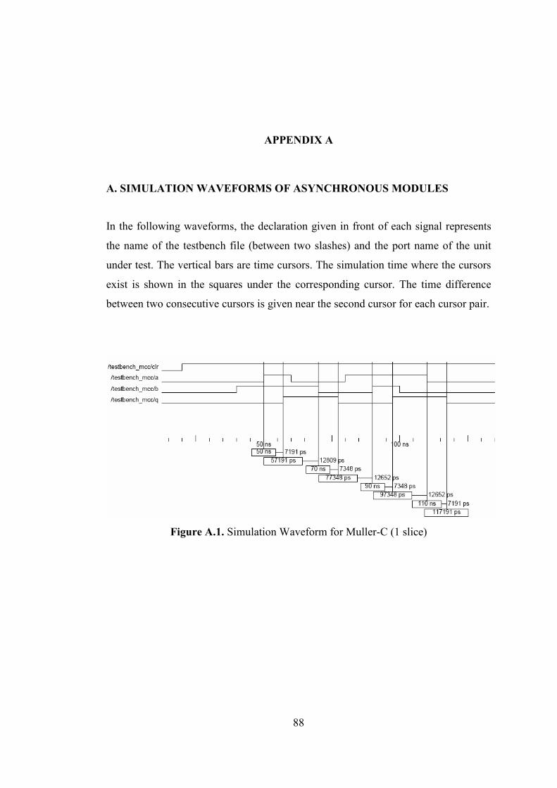
88
APPENDIX A
A. SIMULATION WAVEFORMS OF ASYNCHRONOUS MODULES
In the following waveforms, the declaration given in front of each signal represents
the name of the testbench file (between two slashes) and the port name of the unit
under test. The vertical bars are time cursors. The simulation time where the cursors
exist is shown in the squares under the corresponding cursor. The time difference
between two consecutive cursors is given near the second cursor for each cursor pair.
Figure A.1. Simulation Waveform for Muller-C (1 slice)
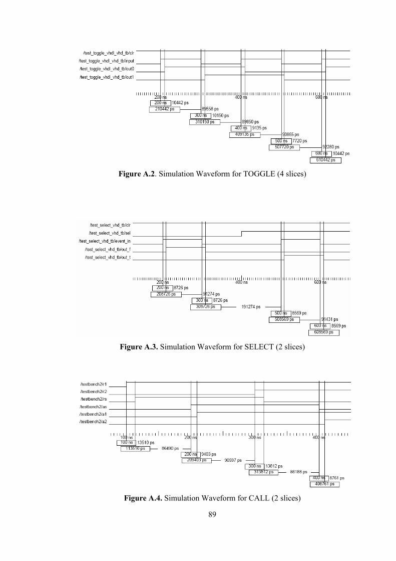
89
Figure A.2. Simulation Waveform for TOGGLE (4 slices)
Figure A.3. Simulation Waveform for SELECT (2 slices)
Figure A.4. Simulation Waveform for CALL (2 slices)
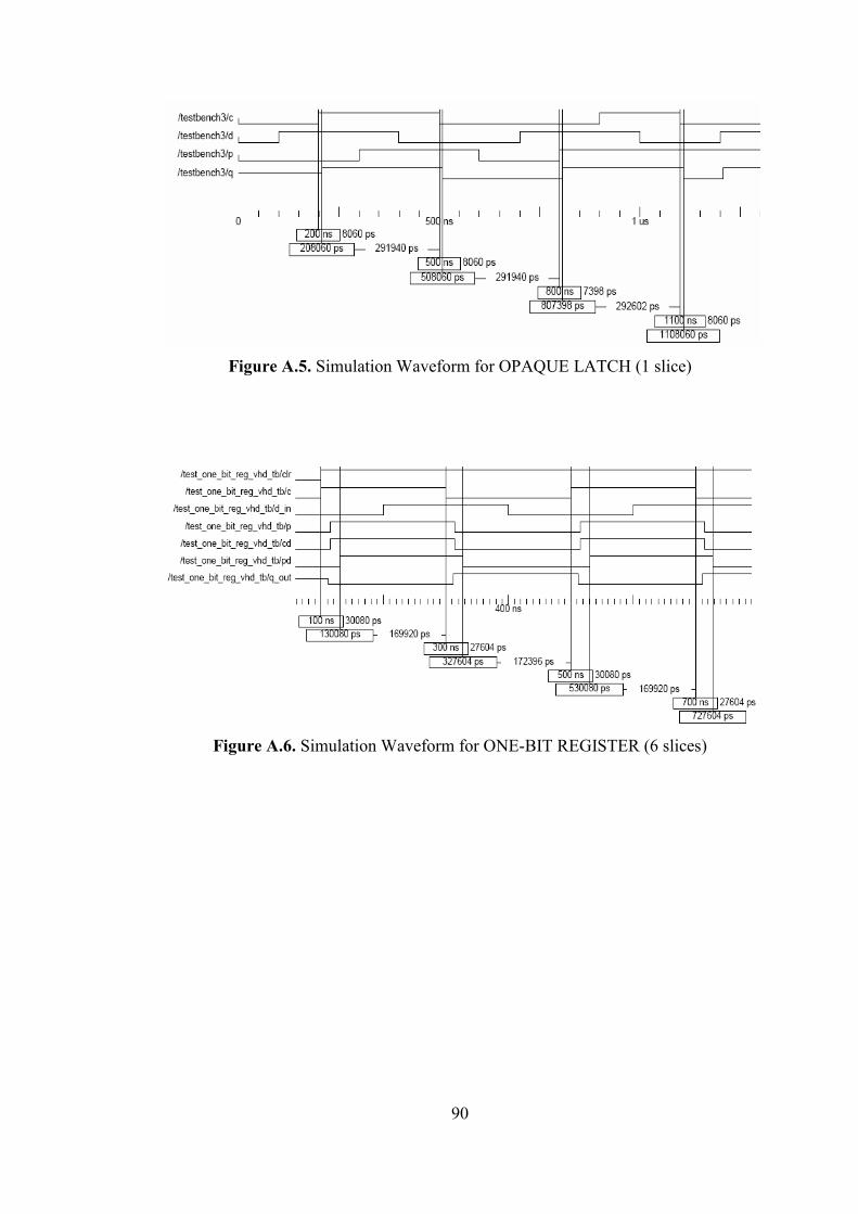
90
Figure A.5. Simulation Waveform for OPAQUE LATCH (1 slice)
Figure A.6. Simulation Waveform for ONE-BIT REGISTER (6 slices)

91
Figure A.7. Simulation Waveform for FOUR-BIT REGISTER (9 slices)
Figure A.8. Simulation Waveform for FOUR-BIT AND (13 slices)
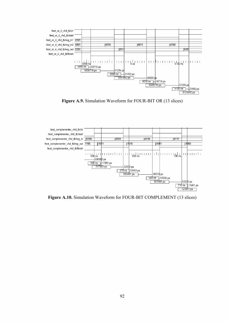
92
Figure A.9. Simulation Waveform for FOUR-BIT OR (13 slices)
Figure A.10. Simulation Waveform for FOUR-BIT COMPLEMENT (13 slices)

93
Figure A.11. Simulation Waveform for PDE (16 slices)
Figure A.12. Simulation Waveform for LOADABLE SHIFT REGISTER (Type 1)
(44 slices)

94
Figure A.13. Simulation Waveform for LOADABLE SHIFT REGISTER (Type 2)
(34 slices)
Figure A.14. Simulation Waveform for MY_MODULE_HF (2 slices)

95
Figure A.15. Simulation Waveform for ADD/SUB (addition) (81 slices)
Figure A.16. Simulation Waveform for ADD/SUB (subtraction) (81 slices)

96
Figure A.17. Simulation Waveform for MULTIPLIER (232 slices)
Figure A.18. Simulation Waveform for DIVIDER (328 slices)

97
APPENDIX B
B. CIRCUIT SCHEMATICS OF THE IMPLEMENTED PCB
Figure B.1 Regulator Circuit
Figure B.2 Power Terminals
98
Figure B.3 FPGA

99
Figure B.4 Input Switches and LEDS
Figure B.5 Debonce Circiut

100
Figure B.6 Input Buffers

101
Figure B.7 Output Buffer and LEDS
Figure B. 8 High Frequency Integrated Circuit Bypass Capacitors

102
Figure B.9 High Frequency I/O Bypass Capacitors
Figure B.10 Mid-frequency Bypass Capacitors

103
Figure B.11 FPGA Programming Interface
104
Figure B.12 Clock Circuit for Synchronous Operation Option

105
Figure B.13 Output Seven-Segment Displays and Driver Circuits

106
Figure B.14 Input Seven-Segment Displays and Driver Circuits
107
Figure B.14 (continued)
108
Figure B.14 (continued)

109
APPENDIX C
C. DESIGN FILES