an analysis of the highly linear transfer characteristics
TRANSCRIPT

An analysis of the highly linear transfer characteristics of dual-buck convertersCitation for published version (APA):Schellekens, J. M., Huisman, H., Duarte, J. L., Hendrix, M. A. M., & Lomonova, E. A. (2018). An analysis of thehighly linear transfer characteristics of dual-buck converters. IEEE Transactions on Industrial Electronics, 65(6),4681-4690. https://doi.org/10.1109/TIE.2017.2772175
DOI:10.1109/TIE.2017.2772175
Document status and date:Published: 01/06/2018
Document Version:Accepted manuscript including changes made at the peer-review stage
Please check the document version of this publication:
• A submitted manuscript is the version of the article upon submission and before peer-review. There can beimportant differences between the submitted version and the official published version of record. Peopleinterested in the research are advised to contact the author for the final version of the publication, or visit theDOI to the publisher's website.• The final author version and the galley proof are versions of the publication after peer review.• The final published version features the final layout of the paper including the volume, issue and pagenumbers.Link to publication
General rightsCopyright and moral rights for the publications made accessible in the public portal are retained by the authors and/or other copyright ownersand it is a condition of accessing publications that users recognise and abide by the legal requirements associated with these rights.
• Users may download and print one copy of any publication from the public portal for the purpose of private study or research. • You may not further distribute the material or use it for any profit-making activity or commercial gain • You may freely distribute the URL identifying the publication in the public portal.
If the publication is distributed under the terms of Article 25fa of the Dutch Copyright Act, indicated by the “Taverne” license above, pleasefollow below link for the End User Agreement:www.tue.nl/taverne
Take down policyIf you believe that this document breaches copyright please contact us at:[email protected] details and we will investigate your claim.
Download date: 18. Mar. 2022
An analysis of the highly linear transfercharacteristics of dual-buck converters
Jan M. Schellekens, Henk Huisman, Senior Member, IEEE, Jorge L. Duarte, Member, IEEE,Marcel A. M. Hendrix Member, IEEE, and Elena A. Lomonova, Senior Member, IEEEof Electrical
Engineering, Eindhoven University of Technology, Eindhoven 5612AZ, The Netherlands,(email:[email protected]).
Abstract— Practical switching devices have finite turn-on and turn-off times. To avoid short circuit, a blankingtime is added between turn-off and turn-on of the comple-mentary working switches in a switching-leg. The blankingtime, also referred to as dead-time, is one of the dominantsources of output current and voltage distortion in pulse-width modulated power amplifiers.
Extensive studies exist on elimination, minimization, andcompensation of the effect. Most techniques achieve areduction of the distortion but are not capable of completelyremoving it. The dual-buck converter does not suffer fromblanking-time-related distortion. However, blanking time isnot the only source of switching-leg-induced distortion.
This paper focuses on the effects of semiconductordevice parameters on the output quality of the dual-buckconverter. It is shown that, ideally, the forward voltages ofthe diodes and switches have no effect on the output qual-ity. Measurements on a prototype, industrial power stackbased, dual-buck converter show a 100 times improvementof the open-loop spurious free dynamic range when com-pared to conventional pulse width modulated converters.
I. INTRODUCTION
BLANKING time is one of the most dominant sourcesof output voltage distortion for pulse width modulated
(PWM) amplifiers based on the conventional switching-legdepicted in Fig. 1a. High-precision applications, like short-stroke linear mechanical actuators for wafer steppers, gradientcoils for magnetic resonance imaging (MRI) systems, andstudio-quality audio, that require better than 80 dB dynamicrange, suffer especially from the blanking-time effect.
Feedback is normally applied in converters to reject distur-bances. The impact of blanking time can indeed be reducedby feedback. However, due to the extremely fast change ofthe output voltage as a function of current and modulationindex, as pointed out in [1] and further detailed in [2], it isnot practical to eliminate the distortion due to blanking timewith feedback only. However, improvements can be gainedby using interleaving or multilevel techniques, as suggestedin many papers including [3]–[5], to allow higher bandwidthand better disturbance rejection of the closed loop convertersystem compared to conventional 2-level PWM converters.
Extensive studies have been done on the elimination [6],minimization [7], and compensation [8]–[10] of blanking timein PWM converters. Most of these techniques rely on thedetection of the polarity of the sampled inductor current ofthe converter and neglect the switching transients.
In [11] a compensation scheme is suggested that includesthe inductor current ripple, and in [12] a more advanced modelof the switch-node commutation was added. All techniquesmentioned above achieve a reduction of the distortion. How-ever, due to errors in the detection of current polarity anddiscontinuous conduction mode (DCM) during zero crossings,they are not capable of completely removing it.
Different modulation techniques have been suggested thatalleviate blanking time effects [6], [7], [9], [13], however, thesemethods also rely on the polarity of the current and do notcompletely remove the impact of blanking time. In [14]–[17]the amount of blanking time is reduced (adaptively or actively)to the absolute minimum at the cost of increased losses.
The resonant pole inverter (RPI) discussed in [18]–[20]features zero-voltage switching (ZVS), and therefore doesnot suffer from blanking-time-related distortion. However, toachieve ZVS the RPI requires considerable circulating cur-rent. Nearly zero-voltage turn-off in the RPI is achieved byreducing the slew rate of the switch-node voltage by addingcapacitance in parallel with the switches. The resulting lowerslew rate during commutation leads to reduced electromagneticinterference (EMI). As a result a well designed RPI does notrequire additional EMI filtering, as is normally required inconventional PWM converters. The slew rate of the switchingtransients, however, is strongly dependent on the operatingpoint of the converter and adds significant distortion.
In practice, the output-voltage quality of RPIs is better thanthat of conventional PWM converters, but not sufficient formany high-precision applications. Furthermore, the hysteresiscontrol scheme of RPIs results in variable switching frequencyand is hard to implement digitally. The RPI is, therefore, rarelyused in industry.
In [21] a circuit consisting of two parallel-connected downconverters, one for positive current and one for negativecurrent, is presented as a high-performance converter thatdoes not suffer from blanking-time-related distortion and isrobust for shoot-through, i.e. unintentional turn-on of twosemiconductor switches simultaneously. It was shown thatwith proper control, low distortion can be achieved, evenwhen nonlinear loads are connected. Later, in [22], the circuitwas introduced as a buck derived PWM power stage withreduced shoot-through current, allowing zero blanking-timeoperation, and was baptized opposed current converter (OCC).Operation of multiple parallel OCC stages was proposed, andit was shown that the topology is suitable for studio-quality

LHB
usn
12UDC
12UDC
C f
S1
D1
D2
S2
iLHB
iout
uout
(a)
usn1 usn2
12UDC
12UDC
S1
D1
D2
S2C f
L f1
iL f1iout
uout
L f2
iL f2
(b)
Fig. 1. Schematic diagrams of (a) the conventional HB switching-leg,and (b) the DB switching-leg, both with output filters.
audio reproduction and high-precision positioning systems. In[23] hysteresis current control was proposed for the OCC,and it was renamed to dual-buck (DB) converter. Later, thesame topology started to appear as split-phase dual-buck [24].In the remainder of this paper the parallel-connected downconverters, as shown in Fig. 1b, will be referred to as DB.
A disadvantage of the DB is that it requires 2 filter inductorsand thus more volume compared to conventional PWM con-verters. Studies show that the total volume can be reduced bycoupling of the inductors [25], by changing the configurationof the inductors [26], or by altering the configuration of theswitching legs [27]. However, the total inductor volume willremain larger than conventional PWM converters by at leastfactor 1.5.
The dual-buck converter does not require blanking time and,therefore, does not suffer from zero-crossing distortion dueto blanking time. However, other phenomena, like nonidealswitches, diodes and inductors, contribute to harmonic distor-tion as well. In conventional converters these effects are, inpractice, often neglected, since their contribution is relativelysmall compared to the effect of blanking time, or simplybecause high accuracy is not an issue. In [28], and moreextensively in [29], different sources of distortion in switchingamplifiers are discussed. These studies focus on the effectsof bipolar junction transistor switches. However, many of theideas can be applied to other types of semiconductor switchestoo. In [30] a detailed analysis of distortion introducedby power metal oxide semiconductor field effect transistors(MOSFETs) in class-D audio amplifiers was made. Thesestudies concentrate on the conventional switching leg, and donot apply to the dual buck converter. In [31] a simulation studyshows that the DB is superior to the conventional half-bridge(HB) converter. The total harmonic distortion (THD) of theDB is shown to be 12 dB better compared to a HB stage withextremely small blanking-time. However, a detailed paper withan analysis of why the DB converter is so much better thanthe conventional HB is still missing.
This paper presents the main results of [25] and focuseson modulation artifacts, the effects of forward voltage andresistance of the semiconductors, and the series resistancesof filter components on the output quality of a DB. It isshown that the average behavior of the DB can be madelinear by proper design. Finally, the theory is verified withmeasurements on a prototype based on an industrial inverter.
II. THE PULSE-WIDTH MODULATED DUAL-BUCKCONVERTER
Fig. 1b depicts a practical implementation of the DBswitching leg with filtering of the PWM voltage waveforms.The switching components that supply positive current tothe load are indicated with subscript 1, and the switchingcomponents that supply negative current are indicated withsubscript 2. Furthermore, the filter inductors have equal values,Lf , and all voltages are referenced to the center terminal ofthe symmetrical DC supply.
The periodic average switch-node voltages 〈usnx〉 can be
determined by applying the state-space averaging method aspresented in [32]. When disregarding losses, assuming con-tinuous conduction mode (CCM) operation, and instantaneousswitching they become
〈usnx〉 = 1
2UDCmx (1)
where the subscript x indicates the corresponding switchingleg, mx is the modulation index, which is limited to theinterval [−1 . . . 1], and UDC is the DC supply voltage of theDB switching leg. From (1) it can be seen that ideally alinear relation exists between the switch-node voltages andmodulation indices when both legs of the DB are operatedin CCM. For discontinuous conduction mode (DCM) thatrelation becomes nonlinear, as shown in [1], and should thusbe avoided for high quality output.
Both legs are effectively operated in parallel and can beanalyzed separately when assuming uCf
constant over oneswitching cycle (Tsw). This is approximately valid because inpractice the series resistance of Cf can be neglected, and Cf ischosen large enough that the output voltage is smooth. Whenassuming uCf
constant and CCM operation, the steady-stateinductor current ripple amplitude (∆iLf
) becomes
∆iLfx= ∆iLf
(1−mx
2)
with (2a)
∆iLf=
UDC
8LfTsw (2b)
where Tsw is the switching cycle time of the PWM, and Lf
is the filter inductance.
A. Decoupling through variable transformationTo ensure CCM under all output conditions, a bias current is
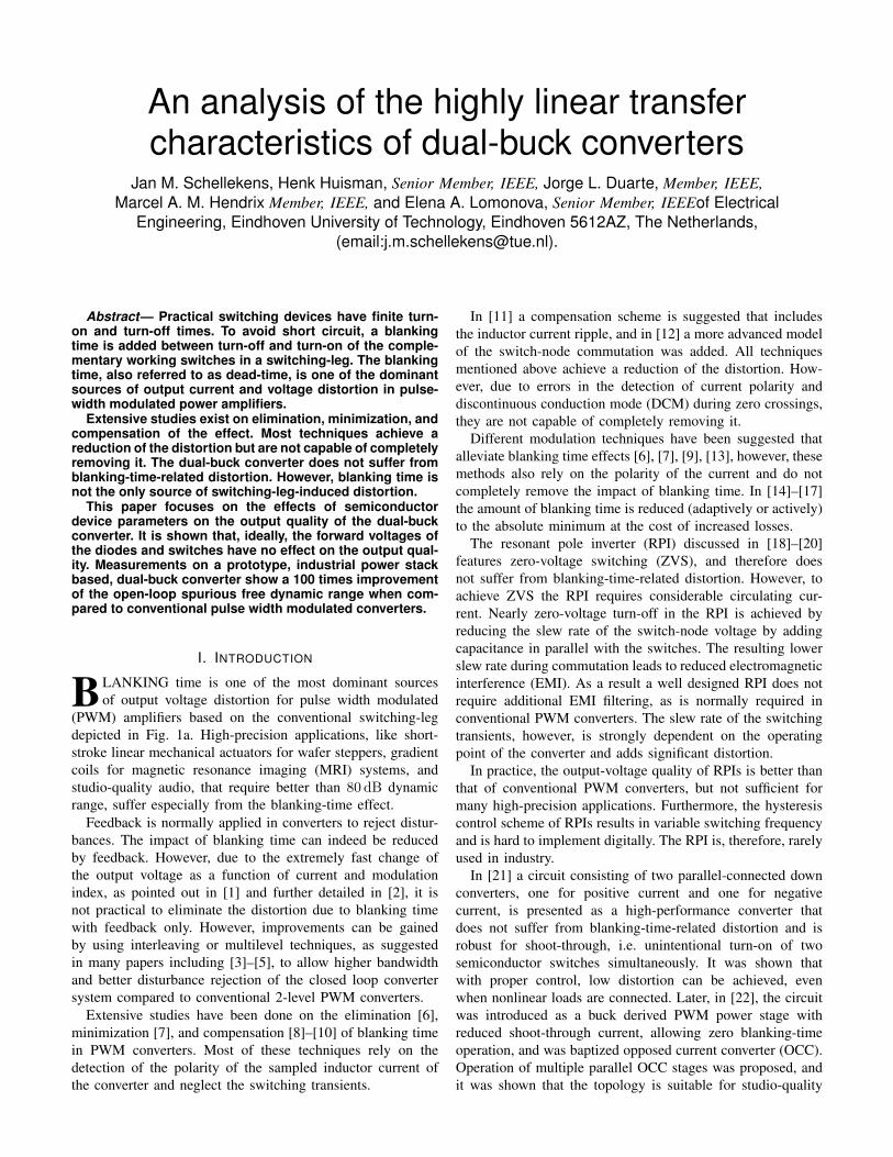
required to flow from the positive-current leg to the negative-current leg. Therefore, it is convenient to separate this biasvoltage and current from the voltage and current that drivesthe output. Doing so leads to decoupled control of the outputpower and the current necessary to maintain CCM. Fig. 2depicts the inductor and output currents, and the output voltageon the left, where the band around the inductor currentrepresents the current ripple of (2a). Note that iLf1
is alwayspositive, and iLf2
is negative. The right graph shows thedecoupled quantities where the voltages are indicated as cycleaverages. The following transformation can be used for thedecoupling:
uavg = 12 (usn1
+ usn2) (3a)
ubias = usn1− usn2
(3b)
5〈ubias〉〈uavg〉
time (s)
uC f
u(V
)
time (s)
ibias
iout
isum
iL f2
iout
iL f1
−ithi(A
)
0 14 To
12 To
34 To To0 1
4 To12 To
34 To To
− 12 UDC
− 14 UDC
0
14 UDC
12 UDC
−iout
0
iout
Fig. 2. Output current and voltage waveforms with constant bias current.
where uavg is the average switch-node voltage of the P- andN-cell, and ubias is the difference between the switch-nodevoltages which drives the bias current. A similar transforma-tion for the currents is given by
isum = iLf1+ iLf2
(4a)
ibias = 12
(iLf1− iLf2
)(4b)
where isum is the combined current of the output filter induc-tors, and ibias is the current required to prevent DCM, andconsequently a nonlinear relation between control input andoutput.
DCM can be prevented by ensuring that the moving averageinductor currents are larger than the corresponding inductorcurrent ripple amplitudes, i.e. 〈iLf1
〉 ≥ ∆iLf1and 〈iLf2
〉 ≤∆iLf2
, basically meaning that
〈ibias〉 ≥ 12 |〈isum〉|+ ith (5)
with
ith ≥
∆iLf2, 〈isum〉 ≥ 0
∆iLf1, 〈isum〉 < 0.
(6)
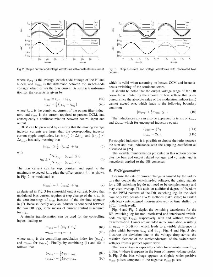
The bias current can be kept constant and equal to themaximum expected isum plus the offset current ith, as shownin Fig. 2, or modulated as
〈ibias〉 = 12 |〈isum〉|+ ith (7)
as depicted in Fig. 3 for sinusoidal output current. Notice thatmodulated bias current requires a step change of the ubias inthe zero crossings of isum because of the absolute operatorin (7). Because ideally only an inductor is connected betweenthe two DB legs, some means of current control is requiredfor ibias.
A similar transformation can be used for the controllinginputs, leading to
mavg = 12 (m1 + m2) (8a)
mbias = m1 −m2 (8b)
where mavg is the controlling modulation index for 〈uavg〉,and mbias for 〈ubias〉. Finally, by combining (1) and (8) itfollows that
〈uavg〉 = 12UDCmavg (9a)
〈ubias〉 = 12UDCmbias (9b)
5〈ubias〉〈uavg〉
time (s)
uC f
u(V
)
time (s)
ibias
iout
isum
iL f2
iout
iL f1
−ithi(A
)
0 14 To
12 To
34 To To0 1
4 To12 To
34 To To
− 12 UDC
− 14 UDC
0
14 UDC
12 UDC
−iout
0
iout
Fig. 3. Output current and voltage waveforms with modulated biascurrent.
which is valid when assuming no losses, CCM and instanta-neous switching of the semiconductors.
It should be noted that the output voltage range of the DBconverter is limited by the amount of bias voltage that is re-quired, since the absolute value of the modulation indices (mx)cannot exceed one, which leads to the following boundarycondition
|mavg|+ 12mbias ≤ 1. (10)
The inductances Lf can also be expressed in terms of Lsum
and Lbias, which for uncoupled inductors equals
Lsum = 12Lf (11a)
Lbias = 2Lf . (11b)
For coupled inductors it is possible to choose the ratio betweenthe sum and bias inductance with the coupling coefficient asdiscussed in [25].
The variable transformation presented in this section decou-ples the bias and output related voltages and currents, and ishenceforth applied to the DB converter.
B. PWM generationBecause the rate of current change is limited by the induc-
tors that couple the switching-leg voltages, the gating signalsfor a DB switching leg do not need to be complementary andmay even overlap. This adds an additional degree of freedomto the PWM patterns of the DB switching leg. In the idealcase only two possible PWM methods make sense; to switchboth legs center-aligned (non-interleaved) or time shifted by12Tsw (interleaved).
Fig. 4 and Fig. 5 depict the switching waveforms for theDB switching leg for non-interleaved and interleaved switch-node voltage (usn), respectively, with and without variabletransformation. Losses are included in the simulation, resultingin ubias = 0.04UDC, which leads to a visible difference inpulse width between usn1
and usn2. Fig. 4 and Fig. 5 also
illustrate the deviation due to the voltage drop across theresistive element of the semiconductors, of the switch-nodevoltages from a perfect square wave.
The bias voltage is especially visible for non-interleaved usn
in Fig. 4 where it appears in the form of narrow voltage peaks.In Fig. 5 the bias voltage appears as slightly wider positiveubias pulses compared to the negative ubias pulses.

iLf 1
iLf 2
usn1
usn2
isum
ibias
uavg
ubias
time (s)time (s)
u(V
)i
(A)
0 2Tsw 4Tsw 6Tsw0 2Tsw 4Tsw 6Tsw
−UDC
− 12 UDC
0
12 UDC
UDC
−ith
0
12 〈iout〉
〈iout〉
Fig. 4. Switching waveforms of the DB switching leg, for non-interleavedusn.
iLf 1
iLf 2
usn1
usn2
isum
ibias
uavg
ubias
time (s)time (s)
u(V
)i
(A)
0 2Tsw 4Tsw 6Tsw0 2Tsw 4Tsw 6Tsw
−UDC
− 12 UDC
0
12 UDC
UDC
−ith
0
12 〈iout〉
〈iout〉
Fig. 5. Switching waveforms of the DB switching leg, for interleaved usn.
When 〈ubias〉 = 0, in case of non-interleaved voltages, asdepicted in Fig. 4, ibias and ubias have no ripple, and isumand uavg have ripple with frequency equal to the switchingfrequency (fsw). For interleaved voltages, as in Fig. 5, thefrequency of the ripple of isum and uavg doubles, and the rippleamplitudes halve. However, a nonzero ripple with fundamentalfrequency equal to fsw appears on ibias and ubias. Conse-quently, there is a trade-off between the effective frequencyand the amplitude of the ripple of uavg and isum on onehand, and the ripple of ubias and ibias on the other hand. Alsonotice that for non-interleaved usn the fundamental switchingfrequency component appears in the bias voltage and current.For interleaved usn the fundamental switching frequency com-ponent appears in uavg and isum when ubias > 0, makinginterleaving less effective for the DB.
III. THE IMPACT OF COMPONENT PARAMETERS ONLINEARITY OF THE DUAL BUCK
In this section the effects of the forward voltages and seriesresistances of the diodes and switches (Vf , Von, Rf , Ron), andthe series resistance (RLf
, RCf) of the filter components (Lf ,
Cf ), are investigated based on the model presented in Fig. 6.Since current can flow only in one direction through the
switch in each of the split legs, antiparallel diodes are notstrictly required. This means that the model depicted in Fig. 6can be applied to investigate the effects of the voltage dropsacross the components for both unipolar current switches, suchas IGBTs, and bipolar-current switches, such as MOSFETs.
L f1
usn1
usn2
S1
D1
D2
S2 L f2
Von1
Vf1
Vf2
Von2
Ron1
R f1
R f2
Ron2
RL f1
RL f1
RC f
C f
iout
12UDC
12UDC
Fig. 6. DB switching leg with parasitic components.
A. Periodically averaged modelThe state-space averaging method is used to derive an
average model that describes the impact of the componentparameters shown in Fig. 6. The following, not yet linearized,averaged state-space representation can be obtained
〈x〉 ≈ 〈A(u)〉〈x〉 + 〈b(u)〉. (12)
where 〈 〉 denotes a switching cycle average value.When the state vector and input vector are chosen to be
x =(iLf1
iLf2uCf
)ᵀ, and (13)
u =(m1 m2 iout
)ᵀ(14)
respectively, the state matrix becomes
〈A(u)〉 =
−R′
1(m1)Lf1
−RCf
Lf1− 1
Lf1
−RCf
Lf2−R′
2(m2)Lf2
− 1Lf2
1Cf
1Cf
0
(15)
with
R′1(m1) = RLf1+RCf
+Ron1 + Ron1−(Rf1−Ron1)m1
R′2(m2) = RLf2+RCf
+Ron2+ Ron2
+(Rf2−Ron2)m2.
Finally, the averaged input vector is determined to be
〈b(u)〉 =
− 1
2 (Vf1+Von1)+1
2 (UDC+Vf1−Von1)m1−RCf
iout
Lf1
12 (Vf2
+Von2)+12 (UDC+Vf2
−Von2)m2+RCfiout
Lf2
− ioutCf
.
(16)
It should be noted that the averaged result is an approxima-tion. However, when 〈A〉 is time-invariant, i.e. when it is nota function of u(t), the averaged model given in (12) exactlydescribes the moving-average behavior of the DB modelpresented in Fig. 6. For the DB the state matrix (15) becomestime-invariant when Rf1 = Ron1
and Rf2 = Ron2, i.e. when
the resistances of the diodes and switched are matched. Thus,when the resistances of the switches and diodes of each legare matched, the cycle averaged behavior of the DB converterleg is linear and can be modeled using state-space averagingwithout error. A full derivation of the average model can befound in [25].

B. Steady-state solutionWhen assuming steady-state, i.e. 〈x〉 = 0, Iout equals
〈ILf1〉 + 〈ILf2
〉, where the capitals represent steady-statevalues as the bottom rows of (15) and (16) are the same,and contain no useful information. The remaining two steady-state equations can be expressed in terms of desired voltagesby application of the transformations given in (4), (8), and byrewriting the modulation indices in desired voltages similarlyas in (8).
The two resulting expressions are straightforward to solvebut the results are lengthy and not insightful. However, whenassuming equal forward voltages and on-resistances for thediodes and switches, i.e. Vf = Vfx , Rf = Rfx , Von = Vonx
,and Ron = Ronx
, with x = 1, 2, the expressions become
U∗avg ≈UDC
2(c + aILf1
) (c− aILf2
) × (kILf1+ lILf2
− a(RLf1
−RLf2
)ILf1
ILf2+ c2UCf
)(17)
and
U∗bias ≈UDC(
c + aILf1
) (c− aILf2
) × (mILf1− nILf2
− a(RLf1+ RLf2
+ Rf + Ron)ILf1ILf2
+ d)
(18)
respectively, where
a = Rf −Ron
b = 12 (Rf + Ron)
c = UDC + Vf − Von
d = (Vf + Von)UDC + V 2f − V 2
on
and
k = bUDC + aUCf+ cRLf1
+ RonVf −RfVon
l = bUDC − aUCf+ cRLf2
+ RonVf −RfVon
m = bUDC − aUCf+ cRLf1
+ RfVf −RonVon
n = bUDC + aUCf+ cRLf2
+ RfVf −RonVon.
Notice that, due to the steady-state assumption, inductancesLf1 and Lf2 , capacitance Cf , and resistance RCf
are elimi-nated from (17) and (18), and that it is a nonlinear approxima-tion because the result is based on a time-variant state matrix.
When R′ = Rf = Ron, (17) and (18) respectively simplifyto
U∗avg =UDC
UDC + Vf − Von
(UCf
+(14 (RLf1
+ RLf2) + 1
2R′) Isum
+ 12
(RLf1
−RLf2
)Ibias
)(19)
and
U∗bias =UDC
UDC + Vf − Von
(Vf + Von
+(RLf1
+ RLf2+ 2R′
)Ibias+
12
(RLf1
−RLf2
)Isum
)(20)
where Isum and Ibias are steady-state currents given by (4).Both (19) and (20) are linear. Furthermore, it can be seen thatthe forward voltages of the semiconductor switches and diodesonly lead to an additional static gain error and, therefore, donot result in harmonic distortion like in conventional switchinglegs, as was already pointed out in [28]. The forward voltageloss, however, needs to be compensated with the bias voltagereference (20) and, therefore, imposes a restriction of themaximum output voltage range of the DB switching leg, aspointed out in (10). There is, however, cross coupling betweenU∗avg and Ibias, and U∗bias and Isum.
By choosing the same series resistances for both inductors,that is RLf
= RLf1= RLf2
, the cross-coupling can beremoved, resulting in
U∗avg =UDC
UDC+Vf−Von
(UCf
+ 12
(RLf
+R′)Isum
)(21)
and
U∗bias =UDC
UDC+Vf−Von
(Vf + Von
+ 2(RLf
+ R′)Ibias
)(22)
respectively, which are both linear and have no cross cou-pling. Matching of the inductors to prevent cross coupling isespecially important for modulated bias current, where ibiasis modulated nonlinearly as given in (5). For constant biascurrent ideally only a static error is added to the outputquantity due to cross coupling. Again, the forward voltagedrops of the switches and diodes only lead to an additionalstatic gain error and not to harmonic distortion.
In practice the series resistances of the switches and diodesare not equal. This can be compensated by matching the resis-tances of the switches and diodes. Adding an extra transistor,which is always on, in series with the diodes, and an additionaldiode in series with the transistors, results in a perfectlymatched switching leg. However, losses will increase. Anothersymmetrization approach is to apply synchronous rectificationby placing switches in parallel with the diodes in the DB leg.The synchronous rectification switches should be switched onwhen the diode would normally conduct.
Experiments with both matched circuits were done in [31]and showed that in practice synchronous rectification givesthe best results for GaN and SiC switches. This is due to thefact that synchronous rectification results in lower effectiveRon and Rf , and consequently smaller difference betweenRon and Rf , compared to matching with series diodes andswitches. Therefore it is important to keep variations betweenthe parasitic resistances, and the filter inductances, static andvarying due to e.g. temperature and saturation, small comparedto the load impedance.
In practice the voltage drop of the diodes and switchesdepends nonlinearly on temperature and current. As such, thetemperatures of the devices need to be matched as close aspossible, which is challenging in reality due to the operating-point dependency of the semiconductor losses. Still, the resultsof this section can be used to calculate precise, operating-point-dependent, steady-state feed-forward references for theDB.

TABLE ICONDUCTION-RELATED PARAMETERS OF SWITCHES, DIODES AND
INDUCTORS (Lf ) USED IN SIMULATIONS.
Von (V) Ron (mΩ) Vf (V) Rf (mΩ) RLf(mΩ)
Matched 1.7 40 1.2 40 50IGBT 1.7 40 1.2 22 50MOSFET 0 109 1.2 22 50
IV. THE IMPACT OF COMPONENT PARAMETERS ONOUTPUT QUALITY OF THE DUAL BUCK
The averaged model is verified using simulation results ofthe DB model depicted in Fig. 6, with a resistive load. Thedevice parameters for the IGBT cases are determined from thedatasheet of the Semikron SKM75GB123D IGBT, the samedevice as used in the experimental setup. For the MOSFETcase, parameters are taken from a 1200 V silicon MOSFETscaled to the same current rating as the IGBT. The diodeparameters for all three cases were taken from the integrateddiode of the IGBT. However, for the matched case Rf waschosen equal to the IGBT’s on-resistance. The parametersused for simulation are summarized in Table I. The switchingtransients were assumed instantaneous for this analysis. Moredetailed results including voltage commutation can be foundin [25].
Fig. 7 depicts the simulated open-loop output voltage spec-trum, for asymmetrical regular-sampled PWM, as described in[33]. The output voltage (uout) that appears across the loadresistance was sinusoidally modulated to half of the voltagerange with a frequency of 21 Hz. The resistive load was chosensuch that the resulting current was also modulated to 50 % ofthe output range, and fsw was 16 kHz, which matches withthe experiments presented later in this paper. The switchesand diodes were modeled as indicated in Fig. 6.
Fig. 7 shows that the matched case does not suffer fromharmonic distortion, as was predicted in the previous section.For constant bias, depicted in Fig. 7a, all harmonics of theIGBT case are smaller than −117 dB, and the third harmonicfor the MOSFET case appears at approximately −100 dB,which is about a factor seven higher than the IGBT case.The harmonic distortion for modulated bias current, depictedin Fig. 7b, is much higher than for constant bias current.That occurs due the impact of unequal Ron and Rf of thesemiconductor devices in (17). The effect of unequal Ron andRf is in this particular case 2 orders of magnitude more severefor modulated ibias than for constant ibias.It should be notedthat the filter inductors were matched in this simulations study,as can be seen from Table I. In [25] the steady-state voltageerror as function of modulation indices and output current iscalculated for constant and modulated ibias, and it is shownthat, especially for small modulation indices, constant bias issuperior over modulated bias. Constant bias current, however,comes at the cost of significant additional losses.
V. EXPERIMENTAL RESULTS
A prototype converter was built that can be configuredas a full-bridge equivalent DB or a conventional full bridge(FB) converter by connecting the switch-nodes of the P- and
Matched
IGBT
MOSFET
harmonic number
mag
nit
ud
e(d
B)
1 3 5 7 9 11
−120
−100
−80
−60
−40
−20
0
(a)
Matched
IGBT
MOSFET
harmonic number
mag
nit
ud
e(d
B)
1 3 5 7 9 11
−120
−100
−80
−60
−40
−20
0
(b)
Fig. 7. Simulated output voltage spectra of a DB switching leg, normal-ized to the output voltage range, with ideal components for (a) constantbias current and (b) modulated bias current.
TABLE IICOMPONENT VALUES USED IN THE EXPERIMENTAL SETUP.
Item Value DescriptionLf 208 µHRLf
50 mΩ
Cf 50 µF Vishay MKP1848650094Y5CfDM
160 µF Vishay MKP1848716704Y5
L 1.7 mH Air-cored inductorR 2.5 Ω 1.5 kW wire wound resistor
N-cell of each side of the full-bridge by means of a relaycontact. Fig. 8 depicts the schematic diagram of the prototypeconverter. The switch nodes can be connected with the relaysdesignated FB. The measured currents, required for feedback,are indicated in the figure.
The nominal component values of the experimental setupare summarized in Table II. The power supply voltage ischosen to be 100 V, low enough to amplify the effects ofthe forward voltages of the switches and diodes. A resistor-inductor load was used to represent the voice-coil actuator thatis often used as load circuit for amplifiers used for short-strokepositioning and studio-quality audio systems. The switchingfrequency was 16 kHz and the duty-ratios are updated twiceper switching cycle. For the full-bridge configuration theblanking time (Tbt) was set to 2 % of Tsw (1.25 µs). The offsetcurrent ith was set to 5.5 A for the DB configuration, whichis enough to guarantee CCM.
Fig. 9 shows details of the experimental setup. The con-verter is based on an off-the-shelf Semikron IGBT stack with6 mF bus capacitance and a custom-designed gate-driver boardbased on Power Integrations SCALE2 drivers. It should benoted that this commercially available stack is by no meansdesigned for generating low distortion waveforms.
UDC
iL f1p
iL f2p
L f
L f
S1p
D1p
D2p
S2p
C f
L R
iout
iL f1n
iL f2n
L f
L f
S1n
D1n
D2n
S2n
C f
RL f RL f
RL fRL f
C fDM
FB FBC f C f
uout
Fig. 8. Schematic overview of the reconfigurable full-bridge equivalentDB and conventional FB setup.
L
FB relaysC fDM
iout
L f
iL f
C f
UDC
IGBT stack
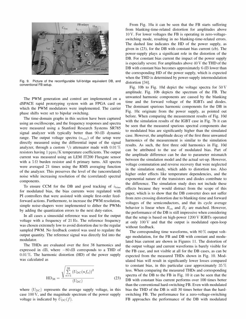
Fig. 9. Picture of the reconfigurable full-bridge equivalent DB, andconventional FB setup.
The PWM generation and control are implemented on adSPACE rapid prototyping system with an FPGA card onwhich the PWM modulators were implemented. The carrierphase shifts were set to bipolar switching.
The time-domain graphs in this section have been capturedusing an oscilloscope, and the frequency responses and spectrawere measured using a Stanford Research Systems SR785signal analyzer with typically better than 90 dB dynamicrange. The output voltage spectra (uout) of the setup weredirectly measured using the differential input of the signalanalyzer, through a custom 1/3 attenuator made with 0.01 %resistors having 1 ppm/K temperature coefficients. The outputcurrent was measured using an LEM IT200 Fluxgate sensorwith a 5 Ω burden resistor and 6 primary turns. All spectrawere averaged 21 times using the RMS averaging functionof the analyzer. This preserves the level of the (uncorrelated)noise while increasing resolution of the (correlated) spectralcomponents.
To ensure CCM for the DB and good tracking of ibiasfor modulated bias, the bias currents were regulated withPI controllers that were assisted with simple first-order feed-forward actions. Furthermore, to increase the PWM resolution,simple noise-shapers were implemented to dither the PWMsby adding the quantization errors to the next duty-ratios.
In all cases a sinusoidal reference was used for the outputvoltage with a frequency of 21 Hz. The reference frequencywas chosen extremely low to avoid distortion due to the regularsampled PWM. No feedback control was used to regulate theoutput quantity. The reference signal was directly fed into themodulator.
The THDs are evaluated over the first 38 harmonics andexpressed in dB, where −80 dB corresponds to a THD of0.01 %. The harmonic distortion (HD) of the power supplywas calculated as
HD38 =
√38∑
n=1(UDC(nfo))
2
〈UDC〉(23)
where 〈UDC〉 represents the average supply voltage, in thiscase 100 V, and the magnitude spectrum of the power supplyvoltage is indicated by UDC(f).
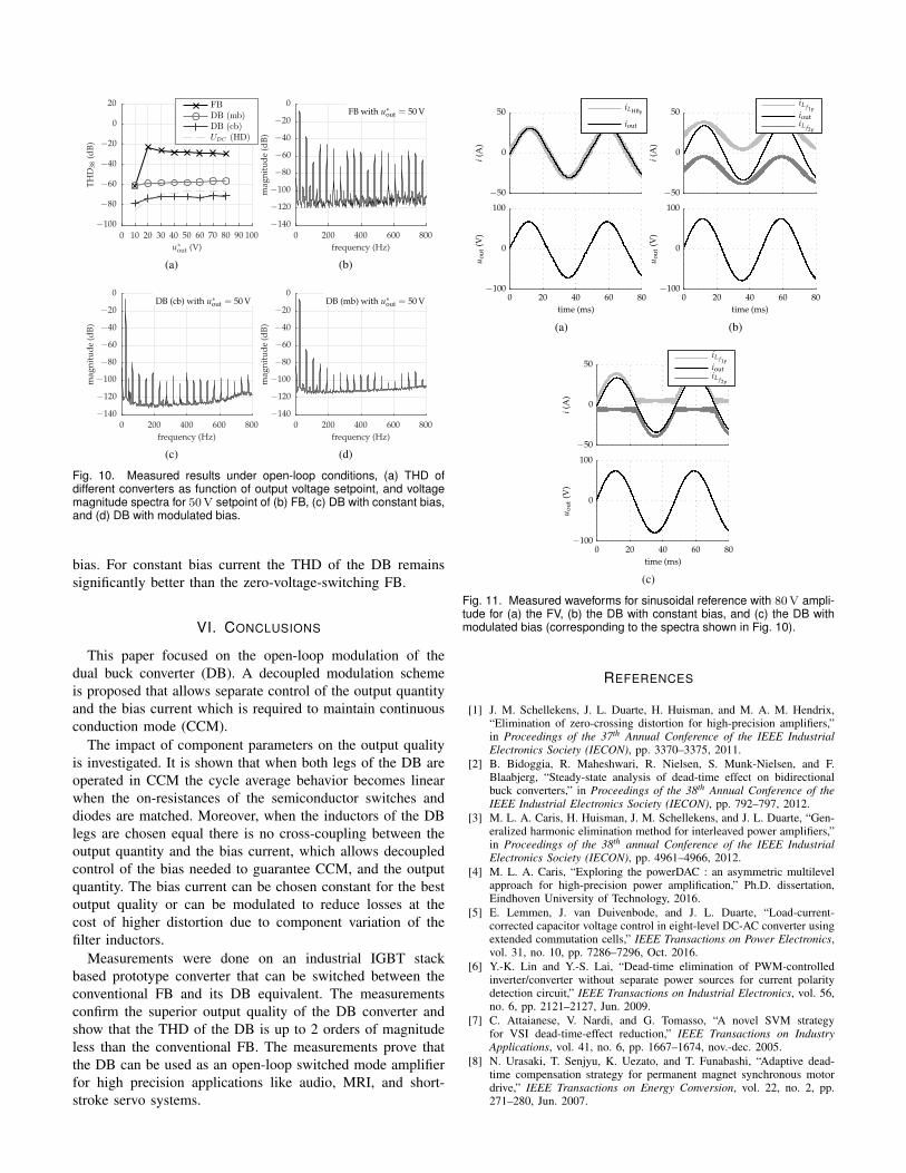
From Fig. 10a it can be seen that the FB starts sufferingfrom blanking-time-related distortion for amplitudes above10 V. For lower voltages the FB is operating in zero-voltage-switching mode, resulting in no blanking-time-related errors.The dashed line indicates the HD of the power supply, asgiven in (23), for the DB with constant bias current (cb). Thepower-supply plays a significant role in the distortion of theDB. For constant bias current the impact of the power supplyis especially severe. For amplitudes above 40 V the THD of theDB with constant bias becomes approximately 6 dB lower thanthe corresponding HD of the power supply, which is expectedwhen the THD is determined by power-supply intermodulationdistortion [34].
Fig. 10b to Fig. 10d depict the voltage spectra for 50 Vamplitude. Fig. 10b depicts the spectrum of the FB. Theunwanted harmonic components are caused by the blankingtime and the forward voltage of the IGBTs and diodes.The dominant spurious harmonic components for the DB inFig. 10c originate from the power supply, as pointed outbefore. When comparing the measurement results of Fig. 10dwith the simulation results of the IGBT case in Fig. 7b it canbe seen that the measured spurious spectral components dueto modulated bias are significantly higher than the simulatedcase. However, the amplitude decay of the first three unwantedharmonics of the measurement is similar to the simulationresults. As such, the first three odd harmonics in Fig. 10dcan be attributed to the use of modulated bias. Part ofthe amplitude difference can be due to parameter mismatchbetween the simulation model and the actual set-up. However,voltage commutation and reverse recovery that were neglectedin the simulation study, which adds to distortion too. Alsohigher order effects like temperature dependencies, and theexponential nature of the transistors and diodes contribute tothe difference. The simulation study does not include theseeffects because they would distract from the scope of thispaper, which is to show that the DB converter does not sufferfrom zero crossing distortion due to blanking-time and forwardvoltages of the semiconductors, and that its cycle averagebehavior is linear when Ron and Rf are matched. However,the performance of the DB is still impressive when consideringthat the setup is based on high-power 1200 V IGBTs operatedat only 100 V and that the output is modulated open-loopwithout feedback.
The corresponding time waveforms, with 80 % output volt-age modulation, for the FB and DB with constant and modu-lated bias current are shown in Figures 11. The distortion ofthe output voltage and current waveforms is barely visible forthe FB case, and not visible at all for the DB cases, as can beexpected from the measured THDs shown in Fig. 10. Mod-ulated bias will result in significantly lower losses comparedto constant bias, in this particular case approximately 35 %less. When comparing the measured THDs and correspondingspectra of the DB to the FB in Fig. 10 it can be seen that theDB with constant bias current performs over 100 times betterthan the conventional hard-switching FB. Even with modulatedbias the THD of the DB is still 30 times better than the hard-switching FB. The performance for a zero-voltage-switchingFB approaches the performance of the DB with modulated
FBDB (mb)DB (cb)UDC (HD)
u∗out (V)
TH
D3
8(d
B)
0 10 20 30 40 50 60 70 80 90 100
−100
−80
−60
−40
−20
0
20
(a)
FB with u∗out = 50 V
frequency (Hz)
mag
nit
ud
e(d
B)
0 200 400 600 800
−140
−120
−100
−80
−60
−40
−20
0
(b)
DB (cb) with u∗out = 50 V
frequency (Hz)
mag
nit
ud
e(d
B)
0 200 400 600 800
−140
−120
−100
−80
−60
−40
−20
0
(c)
DB (mb) with u∗out = 50 V
frequency (Hz)
mag
nit
ud
e(d
B)
0 200 400 600 800
−140
−120
−100
−80
−60
−40
−20
0
(d)
Fig. 10. Measured results under open-loop conditions, (a) THD ofdifferent converters as function of output voltage setpoint, and voltagemagnitude spectra for 50 V setpoint of (b) FB, (c) DB with constant bias,and (d) DB with modulated bias.
bias. For constant bias current the THD of the DB remainssignificantly better than the zero-voltage-switching FB.
VI. CONCLUSIONS
This paper focused on the open-loop modulation of thedual buck converter (DB). A decoupled modulation schemeis proposed that allows separate control of the output quantityand the bias current which is required to maintain continuousconduction mode (CCM).
The impact of component parameters on the output qualityis investigated. It is shown that when both legs of the DB areoperated in CCM the cycle average behavior becomes linearwhen the on-resistances of the semiconductor switches anddiodes are matched. Moreover, when the inductors of the DBlegs are chosen equal there is no cross-coupling between theoutput quantity and the bias current, which allows decoupledcontrol of the bias needed to guarantee CCM, and the outputquantity. The bias current can be chosen constant for the bestoutput quality or can be modulated to reduce losses at thecost of higher distortion due to component variation of thefilter inductors.
Measurements were done on an industrial IGBT stackbased prototype converter that can be switched between theconventional FB and its DB equivalent. The measurementsconfirm the superior output quality of the DB converter andshow that the THD of the DB is up to 2 orders of magnitudeless than the conventional FB. The measurements prove thatthe DB can be used as an open-loop switched mode amplifierfor high precision applications like audio, MRI, and short-stroke servo systems.
uo
ut
(V)
time (ms)
iout
iLHBp
i(A
)
0 20 40 60 80−100
0
100
−50
0
50
(a)
uo
ut
(V)
time (ms)
iL f2p
iout
iL f1p
i(A
)
0 20 40 60 80−100
0
100
−50
0
50
(b)
uo
ut
(V)
time (ms)
iL f2p
iout
iL f1p
i(A
)
0 20 40 60 80−100
0
100
−50
0
50
(c)
Fig. 11. Measured waveforms for sinusoidal reference with 80 V ampli-tude for (a) the FV, (b) the DB with constant bias, and (c) the DB withmodulated bias (corresponding to the spectra shown in Fig. 10).
REFERENCES
[1] J. M. Schellekens, J. L. Duarte, H. Huisman, and M. A. M. Hendrix,“Elimination of zero-crossing distortion for high-precision amplifiers,”in Proceedings of the 37th Annual Conference of the IEEE IndustrialElectronics Society (IECON), pp. 3370–3375, 2011.
[2] B. Bidoggia, R. Maheshwari, R. Nielsen, S. Munk-Nielsen, and F.Blaabjerg, “Steady-state analysis of dead-time effect on bidirectionalbuck converters,” in Proceedings of the 38th Annual Conference of theIEEE Industrial Electronics Society (IECON), pp. 792–797, 2012.
[3] M. L. A. Caris, H. Huisman, J. M. Schellekens, and J. L. Duarte, “Gen-eralized harmonic elimination method for interleaved power amplifiers,”in Proceedings of the 38th annual Conference of the IEEE IndustrialElectronics Society (IECON), pp. 4961–4966, 2012.
[4] M. L. A. Caris, “Exploring the powerDAC : an asymmetric multilevelapproach for high-precision power amplification,” Ph.D. dissertation,Eindhoven University of Technology, 2016.
[5] E. Lemmen, J. van Duivenbode, and J. L. Duarte, “Load-current-corrected capacitor voltage control in eight-level DC-AC converter usingextended commutation cells,” IEEE Transactions on Power Electronics,vol. 31, no. 10, pp. 7286–7296, Oct. 2016.
[6] Y.-K. Lin and Y.-S. Lai, “Dead-time elimination of PWM-controlledinverter/converter without separate power sources for current polaritydetection circuit,” IEEE Transactions on Industrial Electronics, vol. 56,no. 6, pp. 2121–2127, Jun. 2009.
[7] C. Attaianese, V. Nardi, and G. Tomasso, “A novel SVM strategyfor VSI dead-time-effect reduction,” IEEE Transactions on IndustryApplications, vol. 41, no. 6, pp. 1667–1674, nov.-dec. 2005.
[8] N. Urasaki, T. Senjyu, K. Uezato, and T. Funabashi, “Adaptive dead-time compensation strategy for permanent magnet synchronous motordrive,” IEEE Transactions on Energy Conversion, vol. 22, no. 2, pp.271–280, Jun. 2007.
[9] D. Leggate and R. J. Kerkman, “Pulse-based dead-time compensator forPWM voltage inverters,” IEEE Transactions on Industrial Electronics,vol. 44, no. 2, pp. 191–197, Apr. 1997.
[10] G. Pellegrino, R. I. Bojoi, P. Guglielmi, and F. Cupertino, “Accurateinverter error compensation and related self-commissioning schemein sensorless induction motor drives,” IEEE Transactions on IndustryApplications, vol. 46, no. 5, pp. 1970–1978, 2010.
[11] J. M. Schellekens, R. A. M. Bierbooms, and J. L. Duarte, “Dead-time compensation for PWM amplifiers using simple feed-forwardtechniques,” in Proceedings of the XIXth International Conference onElectrical Machines (ICEM), pp. 1–6, 2010.
[12] T. Mannen and H. Fujita, “Dead time compensation method basedon current ripple estimation,” in Proceedings of the IEEE EnergyConversion Congress and Exposition (ECCE), pp. 775–782, 2013.
[13] K. M. Cho, W. S. Oh, Y. T. Kim, and H. J. Kim, “A new switchingstrategy for pulse width modulation (PWM) power converters,” IEEETransactions on Industrial Electronics, vol. 54, no. 1, pp. 330–337, 2007.
[14] M. Berkhout, “A class D output stage with zero dead time,” in Digestof technical papers of the IEEE International Solid-State CircuitsConference (ISSCC), pp. 134–135, 2003.
[15] M. Rose, J. Krupar, H. Guldner, and E. Brenner, “Effects of varyingload conditions on adaptive gate control methods,” in Proc. 2011-14thEuropean Conf. Power Electronics and Applications (EPE 2011), pp.1–7, 2011.
[16] V. Yousefzadeh and D. Maksimovic, “Sensorless optimization of deadtimes in DC-DC converters with synchronous rectifiers,” IEEE Transac-tions on Power Electronics, vol. 21, no. 4, pp. 994–1002, 2006.
[17] Y. Lobsiger and J. W. Kolar, “Closed-loop di/dt and dv/dt controland dead time minimization of IGBTs in bridge leg configuration,” inProceedings of the 14th IEEE workshop on Control and Modeling forPower Electronics (COMPEL), pp. 1–7, Jun. 2013.
[18] D. M. Divan and G. Skibinski, “Zero-switching-loss inverters forhigh-power applications,” IEEE Transactions on Industry Applications,vol. 25, no. 4, pp. 634–643, 1989.
[19] J. Cho, D. Hu, and G. Cho, “Three phase sine wave voltage sourceinverter using the soft switched resonant poles,” in Proceedings ofthe 15th Annual Conference of the IEEE Industrial Electronics Society(IECON), vol. 1, pp. 48–53, Nov. 1989.
[20] R. W. De Doncker and J. P. Lyons, “The auxiliary resonant commutatedpole converter,” in Conference record of the IEEE Industry ApplicationsSociety (IAS) annual meeting, pp. 1228–1235, 1990.
[21] N. R. Zargari, P. D. Ziogas, and G. Joos, “A two-switch high-performance current regulated DC/AC converter module,” IEEE Trans-actions on Industry Applications, vol. 31, no. 3, pp. 583–589, 1995.
[22] G. Stanley and K. M. Bradshaw, “Precision DC-to-AC power conversionby optimization of the output current waveform - the half bridgerevisited,” IEEE Transactions on Power Electronics, vol. 14, no. 2, pp.372–380, Mar. 1999.
[23] J. Liu and Y. Yan, “A novel hysteresis current controlled dual buckhalf bridge inverter,” in Proceedings of the 34th Annual IEEE PowerElectronics Specialist Conference (PESC), vol. 4, pp. 1615–1620, 2003.
[24] C. Zhu, F. Zhang, and Y. Yan, “A novel split phase dual buck halfbridge inverter,” in Proceedings of the 20th Annual IEEE Applied PowerElectronics Conference and Exposition (APEC), vol. 2, pp. 845–849,2005.
[25] J. M. Schellekens, “A class of robust switched-mode power amplifierswith highly linear transfer characteristics, on the elimination of zero-crossing distortion in switching converters,” Ph.D. dissertation, Eind-hoven University of Technology, 2014.
[26] E. Lemmen, J. M. Schellekens, C. G. E. Wijnands, and J. L. Duarte,“Advances in high precision amplifiers - the extra L opposed currentconverter,” IEEE Transactions on Power Electronics, vol. 30, no. 10,pp. 5691–5700, Oct. 2015.
[27] J. M. Schellekens, M. L. A. Caris, J. L. Duarte, H. Huisman, M. A. M.Hendrix, and E. A. Lomonova, “High precision switched-mode amplifierwith an auxiliary bias circuit,” in Proceedings of the 15th EuropeanConference on Power Electronics and Applications (EPE), pp. 1–10,2013.
[28] R. W. Erickson and R. D. Middlebrook, “Origins of harmonic distortionin switching amplifiers,” in Proceedings of the 4th annual InternationalPower Conversion Conference, pp. 567–582, 1982.
[29] R. W. Erickson, “Large signals in switching converters,” Ph.D. disser-tation, California Institute of Technology, 1983.
[30] K. Nielsen, “Audio power amplifier techniques with energy efficientpower conversion, volume I,” Ph.D. dissertation, Technical Universityof Denmark (DTU), 1998.
[31] M. Mauerer, A. Tuysuz, and J. W. Kolar, “Distortion analysis oflow-THD/high-bandwidth GaN/SiC class-D amplifier power stages,” inProceedings of the IEEE Energy Conversion Congress and Exposition(ECCE), 2015.
[32] R. Middlebrook and S. Cuk, “A general unified approach to modellingswitching-converter power stages,” in Proceedings of the IEEE PowerElectronics Specialists Conference (PESC), vol. 1, pp. 18–34, 1976.
[33] D. G. Holmes and T. A. Lipo, Pulse Width Modulation for PowerConverters: Principles and Practice (IEEE Press Series on PowerEngineering). Wiley-IEEE Press, 2003.
[34] M. Berkhout, “An integrated 200-W class-D audio amplifier,” IEEEjournal of solid-state circuits, vol. 38, no. 7, pp. 1198–1206, Jul. 2003.
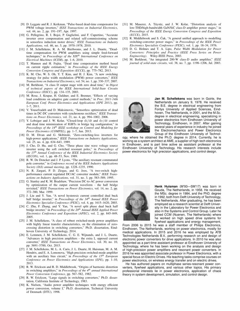
Jan M. Schellekens was born in Goirle, theNetherlands on January 9, 1978. He receivedthe B.E. degree in electrical engineering fromFontys University of Applied Sciences, Eind-hoven, The Netherlands, in 2001, and the M.Sc.degree in electrical engineering, specializing inpower electronics from Eindhoven University ofTechnology, Eindhoven, in 2007. After gainingseveral years of experience in industry he joinedthe Electromechanics and Power ElectronicsGroup of the Eindhoven University of Technol-
ogy, where he obtained the Ph.D. degree in 2014. Currently, he isworking as a system architect at AME, a supplier of high-tech electronicsin Eindhoven, and is part time active as assistant professor at theEindhoven University of Technology. His research interests includepower electronics for high precision applications, and control design.
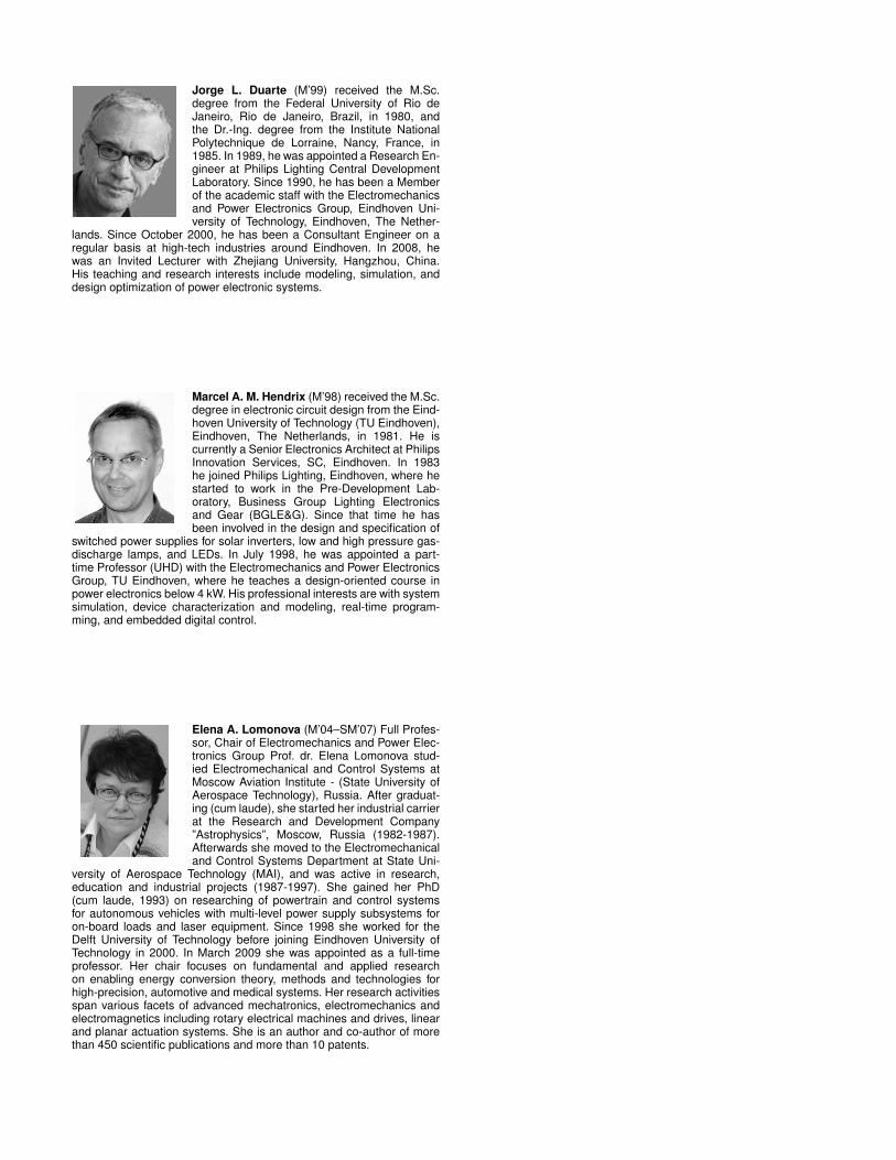
Henk Huisman (M’93—SM’17) was born inGouda, The Netherlands, in 1958. He receivedthe MSc. degree in 1984, and the PhD. degreein 1992, both from Delft University of Technology,The Netherlands. After graduating, he has beenemployed as a research scientist at Delft Univer-sity in the Laboratory for Power Electronics andalso in the Systems and Control Group. Later hejoined CCM (Nuenen, The Netherlands) wherehe worked on high speed drive systems forflywheel applications and energy management.
From 2006 to 2015 he was a staff member of Philips Electronics,Eindhoven, The Netherlands, working on power electronics, mostly formedical applications. In 2015 and 2016 he was employed by ATBTechnologies Netherlands B.V., performing research on and design ofelectronic power converters for drive applications. In 2010 he was alsoappointed as a part-time assistant professor at Eindhoven University ofTechnology, where he has been working on the analysis and designof high-precision power amplifiers and resonant power converters. In2016 he was appointed associate professor in Power Electronics, with aspecial focus on Electric Drives. His teaching tasks comprise courses onpower electronics, on wireless energy transfer and on electric drives.
He has authored papers on multiphase series-resonant power con-verters, flywheel applications, and various other topics. His primaryprofessional interests lie in power electronics, application of chaostheory in system development, simulation, and control design.
Jorge L. Duarte (M’99) received the M.Sc.degree from the Federal University of Rio deJaneiro, Rio de Janeiro, Brazil, in 1980, andthe Dr.-Ing. degree from the Institute NationalPolytechnique de Lorraine, Nancy, France, in1985. In 1989, he was appointed a Research En-gineer at Philips Lighting Central DevelopmentLaboratory. Since 1990, he has been a Memberof the academic staff with the Electromechanicsand Power Electronics Group, Eindhoven Uni-versity of Technology, Eindhoven, The Nether-
lands. Since October 2000, he has been a Consultant Engineer on aregular basis at high-tech industries around Eindhoven. In 2008, hewas an Invited Lecturer with Zhejiang University, Hangzhou, China.His teaching and research interests include modeling, simulation, anddesign optimization of power electronic systems.
Marcel A. M. Hendrix (M’98) received the M.Sc.degree in electronic circuit design from the Eind-hoven University of Technology (TU Eindhoven),Eindhoven, The Netherlands, in 1981. He iscurrently a Senior Electronics Architect at PhilipsInnovation Services, SC, Eindhoven. In 1983he joined Philips Lighting, Eindhoven, where hestarted to work in the Pre-Development Lab-oratory, Business Group Lighting Electronicsand Gear (BGLE&G). Since that time he hasbeen involved in the design and specification of
switched power supplies for solar inverters, low and high pressure gas-discharge lamps, and LEDs. In July 1998, he was appointed a part-time Professor (UHD) with the Electromechanics and Power ElectronicsGroup, TU Eindhoven, where he teaches a design-oriented course inpower electronics below 4 kW. His professional interests are with systemsimulation, device characterization and modeling, real-time program-ming, and embedded digital control.
Elena A. Lomonova (M’04–SM’07) Full Profes-sor, Chair of Electromechanics and Power Elec-tronics Group Prof. dr. Elena Lomonova stud-ied Electromechanical and Control Systems atMoscow Aviation Institute - (State University ofAerospace Technology), Russia. After graduat-ing (cum laude), she started her industrial carrierat the Research and Development Company”Astrophysics”, Moscow, Russia (1982-1987).Afterwards she moved to the Electromechanicaland Control Systems Department at State Uni-
versity of Aerospace Technology (MAI), and was active in research,education and industrial projects (1987-1997). She gained her PhD(cum laude, 1993) on researching of powertrain and control systemsfor autonomous vehicles with multi-level power supply subsystems foron-board loads and laser equipment. Since 1998 she worked for theDelft University of Technology before joining Eindhoven University ofTechnology in 2000. In March 2009 she was appointed as a full-timeprofessor. Her chair focuses on fundamental and applied researchon enabling energy conversion theory, methods and technologies forhigh-precision, automotive and medical systems. Her research activitiesspan various facets of advanced mechatronics, electromechanics andelectromagnetics including rotary electrical machines and drives, linearand planar actuation systems. She is an author and co-author of morethan 450 scientific publications and more than 10 patents.