an-655 application note - analog devices · an-655 application note ... dwdm transmission system...
TRANSCRIPT

AN-655APPLICATION NOTE
One Technology Way • P.O. Box 9106 • Norwood, MA 02062-9106 • Tel: 781/329-4700 • Fax: 781/326-8703 • www.analog.com
FEATURESSingle Board Solution for Tunable Lasers8-Channel Selectable Wavelength ControlWavelength Locking at 25 GHz/50 GHz SpacingAutoPower Control (APC)AutoTemperature Control (ATC)AutoFrequency Control (AFC)Laser Bias, Temperature MonitoringEEPROM-Based AutorestoringSerial Interfaces (SPI®/I2C®/RS-232) to Host SystemWavelength Stability < 2 pm (typ)LD Temperature Stability < 0.01°C
APPLICATIONSDWDM Transmission SystemOptical Instrumentation
GENERAL DESCRIPTIONThis tunable laser reference design offers a single board solution with complete control requirements for DFB tun-able laser subsystems. Designed to work from +3 V/–5 V power supplies, it provides a low cost, low power tunable laser solution designed for ease of use with standard serial control interfaces.
A mixed-signal monolithic microprocessor, the ADuC832- based wave locker feedback loop is designed to meet the requirements of ITU-T grid spacing in a 50 GHz/25 GHz system. An integrated 12-bit ADC with an 8-channel multiplexer allows users to monitor laser bias current and laser temperature via SPI, I2C, or RS-232C serial interfaces. The ADN2830 laser bias controller can sink up to 200 mA (single)/400 mA (dual) and its integrated feedback control loop can maintain output optical power constant over temperature changes during wave lock-ing. The ADN8830 TEC controller enables excellent laser temperature stability and precise wavelength control with 1 pm resolution. A patented PWM/linear based TEC drive architecture enables high efficiency and minimizes external filtering components.
Tunable Laser Reference Design for Designers withthe ADuC832/ADN8830/ADN2830
by Nobuhiro Matsuzoe
FUNCTIONAL BLOCK DIAGRAM
MICROCONVERTER
ADuC832
AUTO-ZEROOP AMPAD8628
AUTO-ZEROOP AMPAD8628
TECCONTROLLER
ADN8830
WAVELENGTHMONITOR PD
TECTHERMISTOR
8 TUNABLE LASER
CW LASERAVERAGE POWER
CONTROLLER
ADN2830
POWERMONITOR PD
ETALONFILTER
2.5VREFERENCE
ADR291
12-BITDAC
12-BITDAC
12-BITSER ADCT/HMUX
GPIOi8051
CWLASER
AD8565
REV. B

–2–
AN-655
–3–
AN-655
WAVELENGTH TUNINGBecause an optical transmitter requires a small form-factor design, use of the refractive index of a semiconduc-tor laser is commonly used to alter the wavelength. As the refractive index can be changed by both the temperature and the density of carriers, transmitter designers can choose from two different types of the wavelength-tunable laser modules—distributed feedback (DFB) lasers and distrib-uted Bragg reflector (DBR) lasers. In general, the DBR laser is capable of a fast tuning speed and a wide tuning range. However, it requires multiple programmable cur-rent sources for wavelength control, which results in a complex system design. In contrast, the DFB lasers can be controlled by temperature of the laser chip, which results in a lower system cost and higher reliability since the DFB lasers are widely used today. The wavelength of the DFB laser is related to temperature with a typical temperature coefficient of 0.1 nm/K. By using a thermoelectric cooler (TEC) and a thermistor with a built-in module, the laser chip temperature can be adjusted, thus wavelength is controlled. Figure 1 shows a simplified block diagram of an optical transmitter designed with the DFB laser. The wavelength tuning range of the DFB laser is limited by an allowable operating temperature range. In fact, DFB lasers provide a tuning range of a couple of nanometers which is equivalent to 8 to 16 ITU-T grid channels depending on the channel-to-channel spacing of the wavelength.
WAVELENGTH LOCKINGThe internal or external wavelength locker generates two monitor signals corresponding to the wavelength and optical output power respectively. The wavelength locker consists of the wavelength selective element and the photodetector diode as shown in Figure 2a. The built-in Fabry Perot etalon works as a wavelength filter which has a periodic characteristic similar to a comb filter. The peak-to-peak range of the etalon filter, referred to as the
Free Spectral Range (FSR) cycle FS, is precalibrated by the manufacturer to align with the ITU grid spacing as shown in Figure 2b. Because the monitor signal has periodic cycles, the algorithm of wavelength locking requires two different tuning methods, coarse tuning, and fine tuning. During the first phase, the laser temperature must settle to the particular temperature corresponding to the target wavelength, where the wavelength is assumed within the capture range. In the case of Figure 2b, there are two locking points on both slopes, positive slope and negative slope, within a single FSR. Thus, the capture range must be half of the SFR. Feedforward control with a look-up table is used in this coarse tuning phase. After the wave-length settles within the capture range, the fine tuning phase acquires the wave length errors between the target wavelength and actual wavelength by monitoring the wave locker signal. Then the wavelength errors will be fed back to the temperature control circuit. The fine tuning phase maintains the wavelength within an allowable wavelength deviation range over ambient temperature changes. The ITU-T recommendation specifies wavelength stability as a frequency deviation in G.692. This deviation is defined as the difference between the nominal central frequency and the actual central frequency (Figure 2c). A maximum frequency deviation is given by
∆f F B
where:
F is the frequency slot
B is the bit rate.
S
S
< ( )– . /2 0 4
In 10 Gbps transmit applications with 50 GHz Grid spac-ing, the frequency deviation f must be less than 7.5 GHz which means wavelength deviation must be less than 67 pm. The test result of the wavelength deviation taken by the reference design is shown in Figure 2d.
THERMISTOR TEC WAVELOCKER
POWERMONITOR
LASERDIODE
MODULATOR
TEC CONTROLLERADN8830
I/VAD8628
LASER CONTROLLERADN2830
ANALOG I/O
MICROPROCESSOR
DIGITAL I/O
SERIAL PORT
MICROCONVERTER ADuC832 I2C LINK TO HOST
2
CONTINUOUSOPTICAL OUT
MODULATEDOPTICAL OUT
TRANSMIT DATA
2
TURNABLE LASER MODULE
Figure 1. Typical Block Diagram of Optical Transmitter with DFB Laser Module
REV. B REV. B

–2–
AN-655
–3–
AN-655
ETALONFILTER
I/V
I/V
OPTICALINPUT
POWERMPD
WAVELENGTH MPD
WAVELENGTH LOCKER
OPTICALOUTPUT
TO µC
TO µC
Figure 2a. Wavelength Locker Block Diagram
WAVELENGTHMONITOR PD
LOCK POINT
WAVELENGTH (nm)
MO
NIT
OR
CU
RR
EN
T (
A
)
POWERMONITOR PDFSR
Figure 2b. Wavelength Locker Characteristics
FS
TUNABLE RANGE = 3nm
F
OP
TIC
AL
PO
WE
R (
dB
)
WAVELENGTH (THz)
Figure 2c. Frequency Slots and AllowableFrequency Deviation
NOTES1. 1-HOUR WAVELENGTH STABILITY AT 25C, WAVE LOCKER ENABLED, 2 SEC INTERVAL.2. F: LOCK POINT 1.5pm MAX TO MIN: 3pm.3. LASER: FLD5F15CA, FUJITSU QUANTUM DEVICES LTD.4. THE WAVELENGTH STABILITY IS MEASURED IN 3pm ACCURACY.5. AFC STABILITY IS AFFECTED BY ACCUMULATIVE ERRORS OF APC AND ATC CONTROL LOOP.
Figure 2d. AFC Typical Performance
DEMONSTRATION BOARDThe tunable laser reference design board (demo board) demonstrates autopower control (APC), autotemperature control (ATC) and autofrequency control (AFC). Figure 3 shows simplified setup of the demo board. The demo board has a mount space for a tunable DFB laser module in a 14-lead butterfly package. The demo board also provides a power supply terminal, analog I/O ports, and a serial port. To mount laser modules, a power photodetector must be floating within the laser module package as seen in Figure 4.
RS-232CCABLE
FC-APC(PANDA FIBER)
LASERMODULE
COMPUTER
POWER SUPPLY(+5V/–5V)
WAVELENGTHMETER
Figure 3. Demo Board Setup
RTHPD1
PD2
7 6 5 4 3 2 1
8 9 10 11 12 13 14
TEC
Figure 4. Laser Module Pin Assignment (refer-ence: Fujitsu Quantum Devices, FLD5F6CA Data Sheet)
REV. B REV. B

–4–
AN-655
–5–
AN-655
GETTING STARTEDTo ensure proper operation, follow the steps below.
1) Calculate the target voltages of the wavelength lock point according to the following equation:
V V R I V
where:
V V
R
LOCKPOINT REF m
REF
= ×( )[ ]
= [ ]= [ ]
–
.
46 2
46
2 50
2490 Ω
The photo current Im2 needs to be solved at each lock point, because the Im2 may differ from lock point to lock point, laser to laser. Table 1 is an example of the calculation result from the 8-channel wavelength tunable laser module.
Table 1.
Wavelength Im2 VLOCKPOINT Lock Point ADC Code
[nm] [THz] [mA] [V] [Dec] [Hex]
0 1582.439 189.4496 521.4 1.202 1969 07B1
1 1582.851 189.4003 573.4 1.072 1757 06DD
2 1583.265 189.3508 511.4 1.227 2010 07DA
3 1583.692 189.2997 563.4 1.097 1798 0706
4 1584.110 189.2498 527.4 1.187 1944 0798
5 1584.529 189.1997 556.8 1.114 1824 0720
6 1584.942 189.1504 524.3 1.194 1957 07A5
7 1585.365 189.1000 553.3 1.122 1839 072F
2) Calculate the voltage setpoint for ADN8830 according to the following equation:
V G T V V
where:
T is target temperature of the thermistor in Celsius.
G =
V V
DAC LASER OFFSET
LASER
OFFSET
= ×( ) [ ]
= [ ]
–
.
– .
0 0658
0 659
Table 2 is an example of the calculation result from the 8-channel wavelength tunable laser module.
Table 2.
CurveWavelength RTH TLASER VDAC DAC Code Slope
[nm] [THz] [] [C] [V] [Dec] [Hex]
0 1582.439 189.4496 16810 12.191 0.144 236 00EC Positive
1 1582.851 189.4003 14370 15.941 0.390 639 027F Negative
2 1583.265 189.3508 12350 19.658 0.634 1040 0410 Positive
3 1583.692 189.2997 10630 23.433 0.883 1447 05A7 Negative
4 1584.110 189.2498 9220 27.106 1.125 1843 0733 Positive
5 1584.529 189.1997 8040 30.728 1.363 2233 08B9 Negative
6 1584.942 189.1504 7060 34.247 1.594 2612 0A34 Positive
7 1585.365 189.1000 6210 37.802 1.828 2996 0BB4 Negative
REV. B REV. B

–4–
AN-655
–5–
AN-655
3) Compile and download the software to the ADuC832. To select the download/debug mode, position the switch (S5) to DEBUG, and then press the reset button (S3).This sets the ADuC832 to download mode. To select the normal mode, posi-tion the switch (S5) to NORMAL and press the reset button (S3). ADuC832 executes downloaded program after reset.
4) Mount the laser module to the mount pads labeled U13. The ADN2830 is capable of sinking a current up to 200 mA. The maximum TEC voltage limit is set at 3.5 V ±5% by default. To change the TEC voltage limiter, change the value of R24 and R25 which is configured as a voltage divider to set the voltage to the VLIM pin of ADN8830. Maximum TEC voltage can be given by:
Maximum TEC voltage V VLIM V= −( ) × [ ]1 5 4. 5) Set JP1 and JP2. To protect the laser module from accidental damage, it is recommended to close JP1 and JP2 if the
program has been changed. Shorting JP1 enables the ADN8830 to shut down mode regardless of control signals from the ADuC832. Shorting JP2 enables the ADN2830 to ALS (Automatic Laser Shutdown) mode regard less of control signals from ADuC832.
6) Apply +3 V and –5 V to the power supply terminal block (J1) located at the top of the demo board.
7) Leave JP2 open. ADN2830 starts to drive the laser diode.
8) Calibrate the optical output power by adjusting the multiturn potentiometer (R48).
9) Leave JP1 open. ADN8830 starts to control the laser temperature to the initial temperature setpoint selected by switch (S4).
10) Press S1 or S2 buttons to change the wavelength lock point. S1 increments and S2 decrements the wavelength point by 1.
11) To change the target wavelength lock point directly, configure the 3-bit DIP switch (S4) according to Table 3. This change is effective only when the ADuC832 is powered up or after reset.
Table 3.
Ch# S4(1) S4(2) S4(3)
0 OFF OFF OFF
1 ON OFF OFF
2 OFF ON OFF
3 ON ON OFF
4 OFF OFF ON
5 ON OFF ON
6 OFF ON ON
7 ON ON ON
12) 7-segment LED (DS1) displays the selected wavelength and DS1 blinks until the laser temperature is set. TEMPLOCK LED (D1) is lit when the laser temperature is settled within the capture range. WL_LOCK LED (D2) is lit when the wavelength
is locked within ITU grid ±12pm.
REV. B REV. B
–6–
AN-655
–7–
AN-655
INTERFACING WAVELENGTH MONITOR PDFigure 5 shows the current-to-voltage conversion circuit on the demo board. The conversion gain is set by R46. The input range of the wavelength monitor current Im2 is up to 1.0 mA by default. The wavelength monitor voltage, Vim2, is calculated by:
V I Vim m2 22 5 2490= ×( )[ ]. –
NOT POPULATEDDAC1
2.5V REF
R570
R58
R46249
Im2
Vm2
AVDO
Figure 5. I/V Conversion Circuit
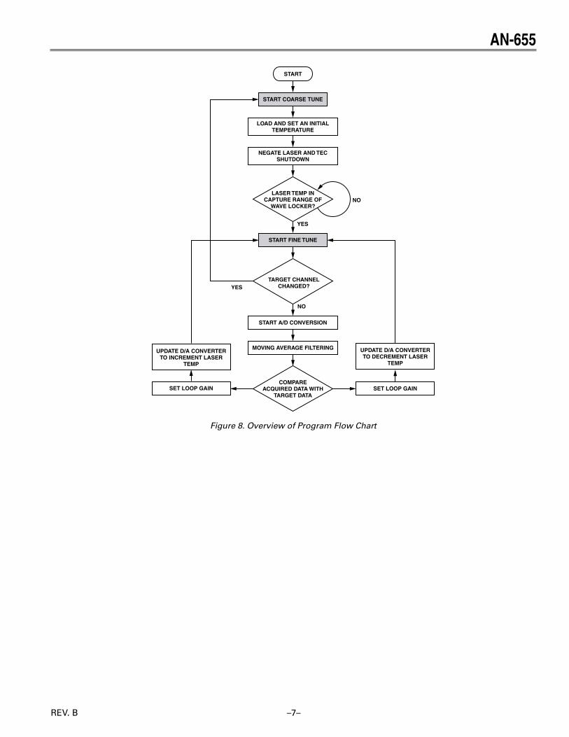
INTERFACING 12-BIT DAC AND ADN8830By using the interface circuit shown in Figure 6, the laser temperature is controlled by DAC output voltage. This scales the DAC voltage range from 0 V to 2.5 V for tem-perature range from 10°C to 50°C. The interface circuit linearizes the thermistor transfer function. The TEMPSET pin of ADN8830 is fixed at 1.25 V. The THERMIN pin is connected to the resistor network which includes the thermistor. The characteristic of voltage-to-temperature is shown in Figure 7.
DAC0R1
TEMPSET
THERMIN
ADN8830
2.5V
ADuC832
RTH
R3
R2
Figure 6. Application Circuit Using DAC Control Voltage
LINEARIZATIONERROR < 0.5%
IDEAL
ACTUAL
2.5
0
CO
NT
RO
L V
OLT
AG
E (
V)
THERMISTOR TEMPERATURE (C)10 50
Figure 7. V-to-Temperature Characteristic
To maintain optimal linearity over the required temperature range, the value of the thermistor resistance should be calculated at the lowest and the highest operating tem-perature according to the following equation:
R = R exp B1T
–1
T
where:
R is thermistor resistance at 25 C.
B is thermistor constant
T is temperature in K.
Typically, B = 3450 and R 10K
TH 25x 25
25
25
25
×
°
=
R1, R2, and R3 are given by:
RR R
R R
RR R
R R
RR R R R – R R
R R R
where:
R R R
R R R
low high
low high
low high
low high
mid high mid low high low
high low mid
high high
low low
12
22
32
2
3
3
=′ ′
′ ′
=′ ′
′ + ′
=+
+
′ = +
′ = +
–
–
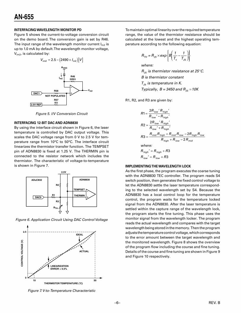
IMPLEMENTING THE WAVELENGTH LOCKAs the first phase, the program executes the coarse tuning with the ADN8830 TEC controller. The program reads S4 switch position, then generates the fixed control voltage to let the ADN8830 settle the laser temperature correspond-ing to the selected wavelength set by S4. Because the ADN8830 has a local control loop for the temperature control, the program waits for the temperature locked signal from the ADN8830. After the laser temperature is settled within the capture range of the wavelength lock, the program starts the fine tuning. This phase uses the monitor signal from the wavelength locker. The program reads the actual wavelength and compares with the target wavelength being stored in the memory. Then the program adjusts the temperature control voltage, which corresponds to the error amount between the target wavelength and the monitored wavelength. Figure 8 shows the overview of the program flow including the course and fine tuning. Details of the course and fine tuning are shown in Figure 9 and Figure 10 respectively.
REV. B REV. B
–6–
AN-655
–7–
AN-655
YES
NO
YES
NO
COMPAREACQUIRED DATA WITH
TARGET DATA
TARGET CHANNELCHANGED?
START COARSE TUNE
MOVING AVERAGE FILTERING
START A/D CONVERSION
NEGATE LASER AND TECSHUTDOWN
LOAD AND SET AN INITIALTEMPERATURE
START FINE TUNE
START
SET LOOP GAIN
UPDATE D/A CONVERTERTO INCREMENT LASER
TEMP
SET LOOP GAIN
UPDATE D/A CONVERTERTO DECREMENT LASER
TEMP
LASER TEMP INCAPTURE RANGE OF
WAVE LOCKER?
Figure 8. Overview of Program Flow Chart
REV. B REV. B

–8–
AN-655
–9–
AN-655
START COARSE TUNE
TEMPERATURELOCKED?
NO
TURN OFFLASER/TEC
LOAD TARGET DATA
READ S4 SWITCH
ADC GAIN/OFFSETCALIBRATION
LOCK POINTCALIBRATION
SET LOCKING SLOPE
SET TARGETTEMPERATURE
TURN ONLASER/TEC
GO TO FINE TUNE
DELAY
Figure 9. Coarse Tuning Flow Chart
REV. B REV. B
–8–
AN-655
–9–
AN-655
START FINE TUNE
CHECK SLOPEPOLARITY
LP < ADCFLAG = 0
GRID CHANNELCHANGED?
8 A/DCONVERSIONS
AVR. FILTERING
LOCKPOINT–ADC
INCREMENT LASERTEMPERATURE
DECREMENT LASERTEMPERATURE
DELAY
ELSE
YES
POSITIVE SLOPE
BACK TOCOARSE TUNE
LP > ADCFLAG = 1
GRID CHANNELCHANGED?
8 A/DCONVERSIONS
AVR. FILTERING
LOCKPOINT–ADC
INCREMENT LASERTEMPERATURE
DECREMENT LASERTEMPERATURE
DELAY
ELSE
YES
NEGATIVE SLOPE
BACK TOCOARSE TUNE
NONO
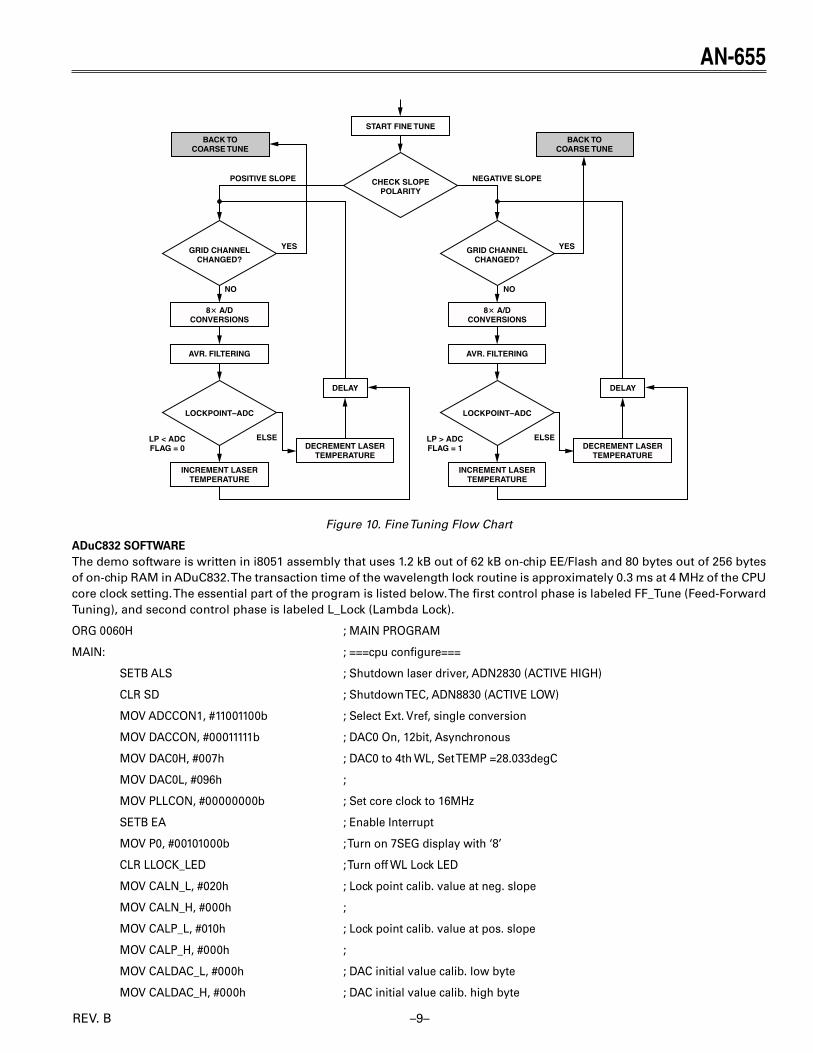
Figure 10. Fine Tuning Flow Chart
ADuC832 SOFTWAREThe demo software is written in i8051 assembly that uses 1.2 kB out of 62 kB on-chip EE/Flash and 80 bytes out of 256 bytes of on-chip RAM in ADuC832. The transaction time of the wavelength lock routine is approximately 0.3 ms at 4 MHz of the CPU core clock setting. The essential part of the program is listed below. The first control phase is labeled FF_Tune (Feed-Forward Tuning), and second control phase is labeled L_Lock (Lambda Lock).
ORG 0060H ; MAIN PROGRAM
MAIN: ; ===cpu configure===
SETB ALS ; Shutdown laser driver, ADN2830 (ACTIVE HIGH)
CLR SD ; Shutdown TEC, ADN8830 (ACTIVE LOW)
MOV ADCCON1, #11001100b ; Select Ext. Vref, single conversion
MOV DACCON, #00011111b ; DAC0 On, 12bit, Asynchronous
MOV DAC0H, #007h ; DAC0 to 4th WL, Set TEMP =28.033degC
MOV DAC0L, #096h ;
MOV PLLCON, #00000000b ; Set core clock to 16MHz
SETB EA ; Enable Interrupt
MOV P0, #00101000b ; Turn on 7SEG display with ‘8’
CLR LLOCK_LED ; Turn off WL Lock LED
MOV CALN_L, #020h ; Lock point calib. value at neg. slope
MOV CALN_H, #000h ;
MOV CALP_L, #010h ; Lock point calib. value at pos. slope
MOV CALP_H, #000h ;
MOV CALDAC_L, #000h ; DAC initial value calib. low byte
MOV CALDAC_H, #000h ; DAC initial value calib. high byte
REV. B REV. B

–10–
AN-655
–11–
AN-655
CALL DACDATA ; Load DAC data table to ram (30h to 3Fh)
CALL LP_DATA ; Load lock point data table to ram (40h to 4Fh)
CALL SW_DETECT ; Read 3-bit DIP SW position
CALL ADCCAL ; ADC Gain and Offset calib.
CALL AUTO_DEMO ; Enable Auto demo if S1/S2 pushed
MOV ECON, #06H ; Erase all pages of data Flash/EE
CALL REV_WRITE ; Write board and firm revision to Flash/EE
FF_TUNE: ; ===Feed-forward tuning (coarse-tune)===
SETB ALS ; Turn off Laser, Active High
CLR SD ; Turn off TEC, Active LOW
CLR PBFLAG ; Clear PBFLAG
CLR P3.6 ; Turn off Temp lock LED
CALL CH_LOAD ; Load selected DAC initial value
CALL LP_LOAD ; Load selected Lock point value
CALL SLOPE_CHECK ; Check slope polarity
MOV P0, WL_SEL ; display selected wavelength ch# on 7seg
SETB LEDBI ; Turn on 7seg display
SETB LEDLE ; 7seg Latch enabled
CALL LP_CAL ; Lock point offset calibration
CALL DAC_CAL ; DAC initial value calibration
MOV DAC0H, DACINT_H ; Update DAC to target temp
MOV DAC0L, DACINT_L ; Update DAC to target temp
SETB SD ; Turn on TEC
CLR ALS ; Turn on Laser
CLR TMPLKFLAG ; Clear temp lock indicate flag
MOV R0, #00H ; SET Page Pointer ADDRESS
MOV R1, #03H ; SET Byte Location ADDRESS
MOV R2, WL_SEL ; SET 1byte Value to write
CALL EE_WRITE ; Call Flash/EE Write routine
CALL TEMP_LOCK ; Sit here until FF_Tune completion
L_LOCK: ; ===Lambda lock Loop (fine tune)===
SETB LEDBI ; Turn on 7seg display
MOV A, #07h ; Set delay time, A*12.5msec
CALL DELAY ; Call delay program, 100msec
JNB SLOPEFLAG, LL_POS ; Check slope polarity, positive or negative
LL_NEG: ; ==Lambda locking at Negative slope==
CALL PB_DETECT ; Detect push-button sw
JNB PBFLAG, LOOP_N ; Jump LOOP_N if PB is not pushed
JMP FF_TUNE ; if PBFLAG=1(PB detected), back to FF_TUNE
LOOP_N:
MOV A, #40d ; Set delay time, A * 12.5msec
REV. B REV. B

–10–
AN-655
–11–
AN-655
CLR P2.7 ; Test signal for cpu transaction monitoring
CALL DELAY ; Call delay program
SETB P2.7 ; Test signal for cpu transaction monitoring
CALL ADC ; Take 8 * samples
CALL AVR ; Averaging
CALL SUBTRACT ; Subtract (LOCKPOINT - ADCDATA)
CALL LOCK_INDICATE ; Turn LED on if result is in lock range
CALL GAIN_DECISION ; Check if error amount is <2LSB, <16LSB
CALL ADJUST_N ; Call dac update routine
CALL LD_BIAS_MONITOR ; Monitor Laser Bias on ADC1
CALL LD_TEMP_MONITOR ; Convert DAC0H/L code to temperature value
CALL CPU_TEMP_MONITOR ; Monitor on-chip temp sensor
JMP LL_NEG ; Back to loop top
LL_POS: ; ==Lambda locking at Positive slope==
CALL PB_DETECT ; Detect push-button sw
JNB PBFLAG, LOOP_P ; Jump LOOP_P if PB is not pushed
JMP FF_TUNE ; if PBFLAG=1(PB detected), back to FF_TUNE
LOOP_P:
MOV A, #40d ; Set delay time, A * 12.5msec
CLR P2.7 ; Test signal for cpu transaction monitoring
CALL DELAY ; Call delay program
SETB P2.7 ; Test signal for cpu transaction monitoring
CALL ADC ; Take 8 * samples
CALL AVR ; Averaging
CALL SUBTRACT ; Subtract (LOCKPOINT - ADCDATA)
CALL LOCK_INDICATE ; Turn LED on if result is in lock range
CALL GAIN_DECISION ; Check if error amount is <2LSB, <16LSB
CALL ADJUST_P ; Call dac update routine
CALL LD_BIAS_MONITOR ; Monitor Laser Bias on ADC1
CALL LD_TEMP_MONITOR ; Convert DAC0H/L code to temperature value
CALL CPU_TEMP_MONITOR ; Monitor on-chip temp sensor
JMP LL_POS ; Back to loop top
; END OF MAIN PROGRAM
REV. B REV. B

–12–
AN-655
–13–
AN-655
SOFTWARE MEMORY MAP
Table 4. Internal RAM, Lower 128 Bytes
Byte Address Byte Name Byte Description
00 to 1F – Reserved
20 Control Flags Detailed in Bit Memory Map
21 WL_SEL Wavelength select
22 CALDAC_L Offset calibration for DAC
23 CALDAC_H
24 CALP_H Offset calibration for positive locking points
25 CALP_L
26 CALN_H Offset calibration for positive locking points
27 CALN_L
28 DACINT_H DAC initial voltage
29 DACINT_L
2A LOCKPOINT_H Wave lock point being selected
2B LOCKPOINT_L
2C RES_H Errors between actual wavelength and target wavelength
2D RES_L
2E DACNEW_L Updated DAC output data
2F DACNEW_H
30 to 4F – Not used
50 AVR_H Averaged wave locker output value
51 AVR_L
52 SUM_H Accumulated wave locker output value
53 SUM_L
54 GAIN Temperature control gain
58 SMPL1_H ADC raw data #1
59 SMPL1_L
5A SMPL2_H ADC raw data #2
5B SMPL2_L
5C SMPL3_H ADC raw data #3
5D SMPL3_L
5E SMPL4_H ADC raw data #4
5F SMPL4_L
60 SMPL5_H ADC raw data #5
61 SMPL5_L
62 SMPL6_H ADC raw data #6
63 SMPL6_L
64 SMPL7_H ADC raw data #7
65 SMPL7_L
66 SMPL8_H ADC raw data #8
67 SMPL8_L
REV. B REV. B

–12–
AN-655
–13–
AN-655
Table 5. Internal RAM, Upper 128 Bytes
Byte Address Byte Name Byte description
80 MSB DAC initial data for channel 1
81 LSB
82 MSB DAC initial data for channel 2
83 LSB
84 MSB DAC initial data for channel 3
85 LSB
86 MSB DAC initial data for channel 4
87 LSB
88 MSB DAC initial data for channel 5
89 LSB
8A MSB DAC initial data for channel 6
8B LSB
8C MSB DAC initial data for channel 7
8D LSB
8E MSB DAC initial data for channel 8
8F LSB
90 MSB Wave lock point data for channel 1
91 LSB
92 MSB Wave lock point data for channel 2
93 LSB
94 MSB Wave lock point data for channel 3
95 LSB
96 MSB Wave lock point data for channel 4
97 LSB
98 MSB Wave lock point data for channel 5
99 LSB
9A MSB Wave lock point data for channel 6
9B LSB
9C MSB Wave lock point data for channel 7
9D LSB
9E MSB Wave lock point data for channel 8
9F LSB
REV. B REV. B

–14–
AN-655
–15–
AN-655
Table 6. Internal RAM Bit Memory Map
Byte Bit Address Bit Name Bit Value Description
20h 00h SLOPEFLAG 1 Negative Lock curve
0 Positive Lock curve
01h RESFLAG 1 Lock Point < ADCDATA
0 Lock Point > ADCDATA
02h TEMPLKFLAG 1 Laser Temperature locked
0 Laser Temperature not locked
03h PBFLAG 1 Button is pushed
0 Button is not pushed
04h – Not used
05h – Not used
06h – Not used
07h – Not used
Table 7. Internal DATA Flash/EE ROM
Byte1 Byte2 Byte3 Byte4
Page 000 Board rev Farm rev Wavelength Grid
Page 001 Laser bias Laser bias Laser temp Laser temp
Page 002 CPU temp CPU temp
Page 003 Not used
:
Page 3FF
REV. B REV. B

–14–
AN-655
–15–
AN-655
APPENDIX [A-1] SCHEMATIC–CPU
AD
C0/
P1.
0/T
2A
DC
1/P
1.1/
T2E
XA
DC
2/P
1.2
AD
C3/
P1.
3A
DC
4/P
1.4
AD
C5/
P1.
5/S
SA
DC
6/P
1.6
AD
C7/
P1.
7
CR
EF
VR
EF
DA
C0
DA
C1
RE
SE
T
P3.
0/R
xDP
3.1/
TxD
P3.
2/IN
T0
P3.
3/IN
T1/
M1S
O/P
WM
1P
3.4/
T0/
PW
MC
/PW
M0/
EX
TC
LK
P3.
5/T
1/C
ON
VS
TP
3.6/
WR
P3.
7/R
DS
CL
OC
KS
DA
TA/M
OS
I
DVDDDVDDDVDDAVDD
AGNDDGNDDGNDDGND
P0.
0P
0.1
P0.
2P
0.3
P0.
4P
0.5
P0.
6P
0.7
XTA
X2
XTA
L1
AL
EP
SE
NE
A
P2.
7/P
WM
1P
2.6/
PW
M0
P2.
5P
2.4
P2.
3P
2.2
P2.
1P
2.0
C24
0.1
F
3420485A
VD
DC
210.
1FC
220.
1FC
230.
1F
PV
DD
6354721
AD
uC
834
43 44 45 46 49 50 51 52 33 32 42 41 40 39 38 37 36 31 30 29 28
1 2 3 4 11 12 13 14
7 8 9 10 15 16 17 18 19 22 23 24 25 26 27
LL
OC
K
U8
DA
C0
15
4 32
AD
8628
AR
T
AV
DD
DA
C1
SW
-PB
S3
R37
1k
PV
DD
PV
DD
JP4
1 2 3 4
HE
AD
ER
4 U
AR
T
JP7
1 2 3 4
HE
AD
ER
4 S
PI/I
2 C
JP3
1 2 3 4
AN
AL
OG
AU
X I/
O
5 6 7
C26
0.1
FR
440
C25
0.1
F
VR
EF
1BM
ON
WL
MO
N
S4
3 2 1
4 5 6
SW
DIP
-3T
EM
PL
OC
K
SD
AL
S
PV
DD
R38
1k
R39
1k
1 32S
5
SW
SP
DT
JP5
HE
AD
ER
2 IC
E
1 2 JP6
HE
AD
ER
2 P
WM
1 2
C27
15p
FC
2815
pF
1 234
Y1
32.7
68kH
z
SW
-PB
S1 SW
-PB
S2
R12
10k
R13
10k
PV
DD
PV
DD
PV
DD
16
INA
INB
INC
IND
LE
BI
LT
VDD
SE
G A
SE
G B
SE
G C
SE
G D
SE
G E
SE
G F
SE
G G
VSS
8
7 1 2 6 5 4 3
U9
13 12 11 10 9 15 14
CD
4511
BC
WM
R49
287
R50
287
R51
287
R52
287
R53
287
R54
287
R55
287
R47
200
PV
DD
a b c d e f g dp
DP
Y a g d
f e
b c
DS
1
dp
cco
mcd
p
DP
Y_7
-SE
G_D
P
9 6
1 10 8 5 4 2 3 7
PV
DD
R1110kR1010kR910kR810kR710kR610k
PV
DD
AL
S: A
CT
IVE
HIG
HS
D: A
CT
IVE
LO
W
Figure 11. Schematic–CPUREV. B REV. B

–16–
AN-655
–17–
AN-655
APPENDIX [A-2] SCHEMATIC–TEC CONTROL
TE
MP
OU
TN
C
TH
ER
MFA
ULT
TH
ER
MIN
TE
MP
SE
TT
EM
PL
OC
KN
CV
RE
F
VL
IMV
TE
C
TE
MP
CT
LC
OM
PF
BC
OM
PO
UT
PVDDPGND
AVDDAGND
PH
AS
ES
YN
CO
UT
SO
FT
STA
RT
FR
EQ
SY
NC
INO
SC
OU
TA N1
P1
OU
TB N2
P2
SW
INS
WO
UT
2023
C2
0.1
F
830
AD
N88
30
29 28 27 26 25 24 19 22 21 9 10 11 18 17
31 32 1 2 3 4 5 6 7 15 16 12 13 14
LL
OC
K
C7
0.1
F
JP1
JUM
PE
R1 2
R2
10k
PV
DD
AV
DD
C10
10n
F
C9
1F
R26
1M
R27
205k
R28
100k
C
1433
0pF
C15
10
F
R24
150k
R25
1k
PV
DD
R21
10k
C5
0.1
F
SD
SH
OR
T J
P1
SH
UT
DO
WN
TE
C[S
D: A
CT
IVE
LO
W]
SD
A1
B1
Q2
CE
XT
2R
CE
XT
2D
GN
D
DV
CC
RC
EX
T1
CE
XT
1Q
1Q
2
B2
A2
CL
R1
Q1
CL
R2
U1 MM
74H
C12
3AM
PV
DD
PV
DD
1 2 3 4 5 7 86
16 12 11 10 914 1315P
VD
D
123
4
5
U11
YB A
NC
7S32
NC
VIN
NC
GN
D
NC
VO
UT
NC
NC
1 3 428 7 6 5
U2
AD
R29
1GR
U
AV
DD
C1
0.1
F
R20
10k 1%
R22
14.7
kR
1736
.5k
R18
24k
R19
8.2k
TH
DA
C0
TE
MP
LO
CK
VR
EF
PV
DD R1
10k
C4
0.1
F
R14
150
PV
DD
1
23Q
1F
DV
301N
R15
150
PV
DD
1
232Q
2F
DV
301N
D1
LE
D (
G)
D2
LE
D (
R)
1
R23
150k
C3
0.1
F
AV
DD
FD
W25
20C
Q5
PV
DD
C6
0.1
F7 6 58
1 2 3 4
L1
C8
22
FC
DE
ES
RD
TE
C–
4.7
F
FD
W25
20C
Q6
PV
DD
C11
10n
F7 6 58
1 2 3 4
L1
C13
3.3n
F
TE
C+
4.7
FC
122.
2nF
Figure 12. Schematic–TBC Control
REV. B REV. B

–16–
AN-655
–17–
AN-655
APPENDIX [A-3] SCHEMATIC–LASER CONTROL
TE
C–
R57 0
WL
MO
N
VR
EF
AV
DD
U7
AD
8628
AR
T2
1
54 3R
462.
49k
0.1%
R58 0
DA
C1
LD
_CL
D_C
LD
_A/G
ND
PD
1_A
PD
1_C
PD
2_C
PD
2_A
TE
C–
TE
C+
TH
TH
NC
NC
GND
3 12 13 4 5 8 9
7 6 1 2 10 14
FL
D5F
15
U6
AV
DD
TH
TE
C+
R42 0
R43
0
R45
1k V
SSR
485k
R41
0
VS
S
R40
1.24
k
VS
S
28 31 5 4 16 15 3 32 26 2
IBIA
SIB
IAS
IMP
DP
SE
T
NC
NC
NC
NC
NC
AS
ET
GNDGNDGND
GNDGNDGND
GNDVCCVCCVCCVCCVCC
IMP
DM
ON
IBM
ON
IBM
ON
PAV
CA
PPA
VC
AP
AL
SM
OD
E
NC
FAIL
DE
GR
AD
E
AD
N28
30
VS
S
302627
72214
1
811122125
6 23 24 9 10 20 17 13 19 18
VS
SR
361k
V
SS
R36
1k
R32
100k
VS
SR16
150
D3
LE
D (
R)
Q4
FD
V30
1N
1 32 2
1IM
PD
MO
N D
ISA
BL
E: R
42-S
HO
RT,
R43
-OP
EN
, R41
-SH
OR
TIM
PD
MO
N E
NA
BL
E: R
42-O
PE
N, R
43-S
HO
RT,
R41
-OP
EN
R31
100k
AV
DD A
D85
65A
KS
21
5
4 3U
4
VS
S
VS
S
R30
100k
R
2910
0k
IBM
ON
VS
SC20
0.1
F
R34
10k
JP2
HE
AD
ER
2
12
R4
10k
VS
SQ3
FD
V30
1N
Q7
FD
V30
4P
VS
SR5
10k
R33
3k
PV
DD
R3
10k
PV
DD
1
1
32
23
AL
S
SH
OR
T J
P2
TOS
HU
TD
OW
N L
AS
ER
[AL
S: A
CT
IVE
HIG
H]
Q7
GA
TE
HIG
H: A
LS
AC
TIV
EQ
7 G
AT
E L
OW
: AL
S D
ISA
BL
E
C16
10n
FC
1710
nF
C18
10n
FC
1910
nF
VS
S
11
Figure 13. Schematic–Laser Control
REV. B REV. B

–18–
AN-655
–19–
AN-655
APPENDIX [A] SCHEMATIC–POWER SUPPLY
J1
321
TERMINALBLOCK D4
LED (G)
R56150
C29100F
C3122F
AVDDPVDD L210F
1
2
1
21
2
C30100F
C3222F
VSSL310F
2
1
2
1
–5V
Figure 14. Schematic–Power Supply
APPENDIX [B] PCB LAYOUT
Figure 15. Top Layer
Figure 16. AGND/PGND Planes
Figure 17. Bottom Layer
Figure 18. AVDD/PVDD/VSS Planes
REV. B REV. B

–18–
AN-655
–19–
AN-655
Figure 19. Top Overlay
APPENDIX [C] BILL OF MATERIALS
Provided as a software copy.
APPENDIX [D] SOFTWARE SOURCE CODE
Provided as a software copy.
REFERENCESAnalog Devices, ADuC832 Data SheetAnalog Devices, ADN8830 Data SheetAnalog Devices, ADN2830 Data SheetFujitsu Quantum Devices, FLD5F6CA Data SheetFujitsu Quantum Devices, FLD5F15CA Data SheetITU-T G.692
REV. B REV. B

E03
717–
0–8/
04(B
)
–20–© 2004 Analog Devices, Inc. All rights reserved. Trademarks and registered trademarks are the property of their respective owners.
Purchase of licensed I2C components of Analog Devices or one of its sublicensed Associated Companies conveys a license for the purchaser under the Philips I2C Patent Rights to use these components in an I2C system, provided that the system conforms to the I2C Standard Specification as defined by Philips.