amusan ms thesis - etd - electronic theses &...
TRANSCRIPT

ANALYSIS OF SINGLE EVENT VULNERABILITIES IN A 130 nm CMOS
TECHNOLOGY
By
Oluwole Ayodele Amusan
Thesis
Submitted to the Faculty of the
Graduate School of Vanderbilt University
in partial fulfillment of the requirements
for the degree of
MASTER OF SCIENCE
in
Electrical Engineering
December, 2006
Nashville, Tennessee
Approved:
Professor Lloyd W. Massengill
Professor Arthur F. Witulski
Professor Bharat L. Bhuva

2
ACKNOWLEDGMENTS
First and foremost, I will like to thank God for the strength to make it this far. I would
like to thank Dr. Lloyd W. Massengill, Dr. Arthur. F. Witulski and Dr. Bharat L. Bhuva,
for believing in me, and for the support and guidance provided while completing my
masters degree. Also, I would like to acknowledge A. L. Sternberg, M. L. Alles, J. D.
Black, P. R. Fleming and R. D. Schrimpf for their contributions to this work.
Additionally, I would like to thank Mark Baze and Warren Snapp of Boeing SSED for
their support and technical collaboration, and DARPA Radiation Hardened by Design
Program for the financial support for the work presented in this thesis. Special thanks to
all my friends from the Radiation Effects and Reliability Group who have helped out in
one way or another.
I would like to thank my friends S. N. Maxey, J. Hill and J. E. Hunter for their words of
encouragement. Finally, very special thanks to my parents Michael and Susannah and my
adopted parents Amos and Janice for their unconditional support and love.

iii
TABLE OF CONTENTS
Page
ACKNOWLEDGMENTS............................................................................................... ii
LIST OF TABLES ......................................................................................................... iv
LIST OF FIGURES..........................................................................................................v
Chapter
I. INTRODUCTION................................................................................................1
II. CHARGE COLLECTION....................................................................................3
Modeling and Calibration of 130 nm CMOS devices .................................3
Effective Collection Depth ..........................................................................9
Parasitic Bipolar Effects ............................................................................13
Single Event Effects in a 130 nm D Flip-Flop...........................................15
III. CHARGE SHARING.........................................................................................21
Introduction................................................................................................21
Charge Sharing Mechanisms .....................................................................21
Simulation Setup........................................................................................22
Simulation Results .....................................................................................23
Mitigation Techniques ...............................................................................29
Conclusion .................................................................................................34
IV. SINGLE EVENT EFFECTS IN A 130 nm DICE LATCH ...............................35
Introduction................................................................................................35
DICE Design and Single Event Upset Exposure .......................................36
Circuit and 3D TCAD Simulation Approach.............................................38
Conclusion .................................................................................................49
V. CONCLUSION ..................................................................................................50
Appendix
A. Devise file for NMOS ........................................................................................52
B. Devise file for PMOS .........................................................................................60
C. Dessis file for 3D mixed-mode D Flip Flop simulation .....................................68
D. Dessis file for 3D mixed-mode DICE latch simulation .....................................78
REFERENCES ...............................................................................................................89

iv
LIST OF TABLES
Table Page
1. Device properties for the calibrated IBM 8RF NMOS and PMOS devices. ...........6
2. List of sensitive node pairs for DICE latch............................................................40
3. Simulation results for NMOS pair .........................................................................47
4. Simulation results for PMOS pair..........................................................................47
5. Simulation results for NMOS-PMOS pair.............................................................47
6. Simulation results for PMOS-NMOS pair.............................................................48
7. 3D Mixed-mode simulation results vs. Heavy ion data.........................................49
v
LIST OF FIGURES
Figure Page
1. 3D TCAD structure of IBM 8RF NMOS device .....................................................4
2. 3D TCAD structure of IBM 8RF PMOS device......................................................5
3. 2D Cross-section of IBM 8RF NMOS device .........................................................5
4. 2D Cross-section of IBM 8RF PMOS device..........................................................6
5. NMOS IdVg curves of 3D TCAD model vs. IBM 130 nm Compact Model ...........7
6. PMOS IdVg curves of 3D TCAD model vs. IBM 130 nm Compact Model ............8
7. NMOS IdVd curves of 3D TCAD model vs. IBM 130 nm Compact Model ...........8
8. PMOS IdVd curves of 3D TCAD model vs. IBM 130 nm Compact Model ............9
9. Methodology for measuring effective collection depth, simulation conducted with
varying strike depths ..............................................................................................10
10. Simulation results show that the effective collection depth for PMOS is
~ 0.9 µm.................................................................................................................11
11. Simulation results show that the effective collection depth for NMOS is
~1.2 µm..................................................................................................................11
12. Microbeam data shows the collected charge at the drain for 36MeV oxygen ions
(7 MeV/mg/cm2) normally incident to the surface. The active diffusion is bounded
by the dotted lines and extends from 3.5 µm to 13.5µm. From these data, a charge
collection depth of 1 µm was estimated, after Tipton, et al., [10] .........................12
13. The NMOS device has a lateral parasitic npn bipolar transistor, the PMOS device
has a lateral parasitic pnp bipolar transistor...........................................................13
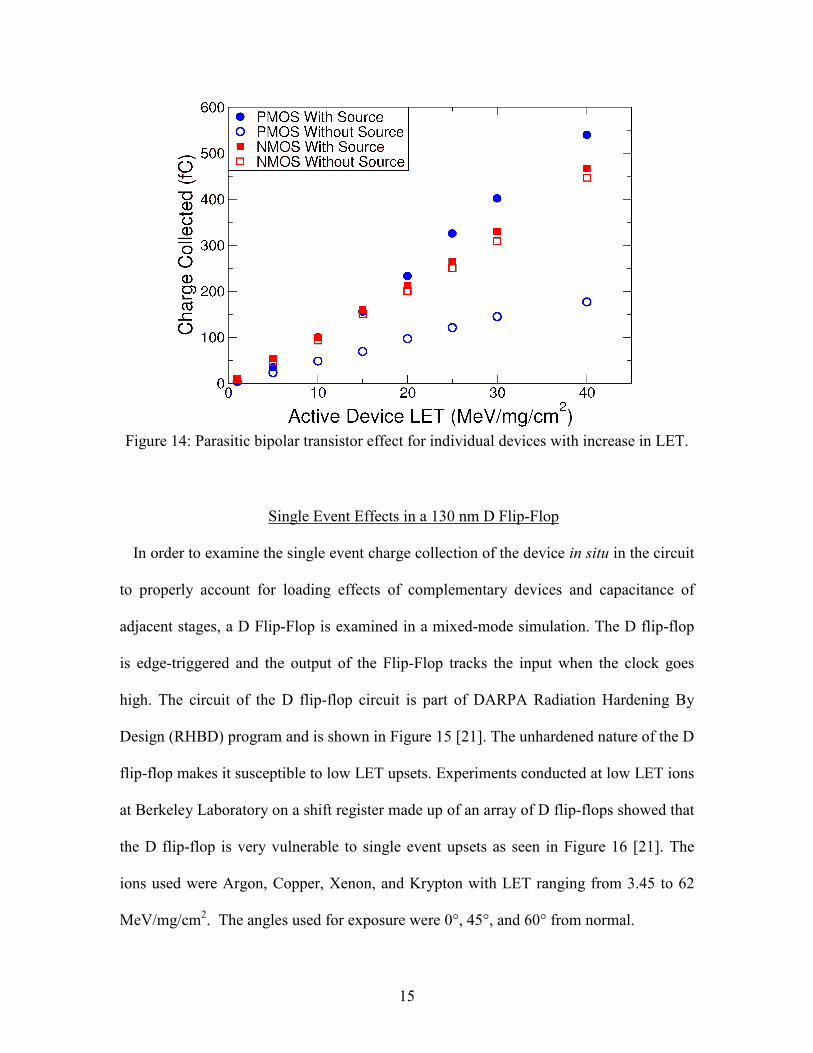
14. Parasitic bipolar transistor effect for individual devices with increase in LET.....15
15. Boeing Standard D Flip-Flop for 2005 test chip, the circled device is the sensitive
NMOS device MN16 .............................................................................................17
16. D Flip-Flop Cross-section, after Baze, et al., [21] .................................................18
vi
17. Current pulse for MN16 drain with and without loading effects...........................19
18. Charge collection for MN16 drain with and without loading effects ....................19
19. Waveforms from the mixed-mode simulation of the D Flip-flop: The state of the
input signal is clocked in and held at the output at every clock rising edge but due
to the ion strike that occur at 36 ns, the output goes low.......................................20
20. Nodal separation setup for NMOS charge sharing ................................................23
21. Charge collection with distance of 0.18 µm between adjacent devices.................24
22. Nodal separation of two PMOS devices, Passive PMOS charge collection shows a
decrease in charge collection with increase in distance.........................................25
23. Nodal separation of two NMOS devices, Passive NMOS charge collection shows
a decrease in charge collection with increase in distance ......................................26
24. Parasitic bipolar amplification effects for Passive devices....................................27
25. Parasitic bipolar amplification of the drain current in passive PMOS device, LET
= 40 MeV/mg/cm2.................................................................................................27
26. Charge collection for Passive NMOS (PMOS active) and Passive PMOS (NMOS
active).....................................................................................................................28
27. The contacted guard-band is highly effective in mitigating PMOS charge
sharing....................................................................................................................30
28. The contacted guard-band is marginally effective in mitigating NMOS charge
sharing....................................................................................................................31
29. Active PMOS and Passive PMOS devices separated by a P-Well ........................32
30. The use of contacted guard-band for PMOS charge sharing is more effective
compared to the use of separate wells....................................................................32
31. Interdigitation to mitigate NMOS charge sharing .................................................33
32. The less-sensitive node collects most of the diffusion charge, thereby reducing the
Passive node charge collection ..............................................................................34
33. Master stage of the DICE cell ................................................................................36
34. Data show DICE upsets at LET values well below theoretical expectations, after
Baze, et al,[21] .......................................................................................................37
vii
35. An Excerpt showing layout proximity of sensitive NMOS-NMOS node pair
MN28-MN18 in the DICE layout ..........................................................................41
36. An Excerpt showing layout proximity of sensitive PMOS-PMOS node pair
MP229-MP28 in the DICE layout .........................................................................42
37. An Excerpt showing layout proximity of sensitive NMOS-PMOS node pair
MN30-MP25 in the DICE layout...........................................................................42
38. Upset/No-Upset SHMOO plot for each sensitive NMOS pair quantifies the charge
sharing necessary for upset, after Sternberg, [28]..................................................43
39. Upset/No-Upset SHMOO plot for each sensitive PMOS pair quantifies the charge
sharing necessary for upset, after Sternberg, [28]..................................................44
40. Upset/No-Upset SHMOO plot for each sensitive NMOS-PMOS pair quantifies
the charge sharing necessary for upset, after Sternberg, [28] ................................44
41. 3D TCAD layout of simulated NMOS-NMOS node pair MN28-MN18 ..............45
42. 3D TCAD layout of simulated PMOS-PMOS node pair MP22-MP28.................46
43. 3D TCAD layout of simulated NMOS-PMOS node pair MN30-MP25................46

1
CHAPTER 1
INTRODUCTION
Single Event Effects (SEE) are caused by the interaction of ionizing particles with
semiconductor devices. The passing of an ionizing particle through a semiconductor
device generates electron-hole pairs (ehps) along the track path and may be collected at
the terminals of a device. Linear Energy Transfer (LET) is defined as the energy loss per
unit path length, normalized by the density of the material. LET has units of
MeV/mg/cm2. A calculation of the charge deposited per unit length can be determined if
the LET of the ion, average energy needed to create an ehp for a material, and density of
the material are known [1]. For silicon, an ion with a LET of 97 MeV/mg/cm2 will
deposit 1pC of charge per micron length of the ion track [2].
The charge collection process in semiconductor devices normally occur in reversed-
biased p/n junctions due to the presence of the high electric field in the reverse-biased
junction depletion region (drift collection). Diffusion collection process is due to the
presence of carriers outside of the depletion region that can diffuse back toward the
junction. Bipolar amplification process is another collection mechanism. This collection
mechanism is due to a lowering of the body potential and turns-on of a parasitic bipolar
transistor for CMOS submicron technologies [3]
Single Event Upsets (SEU) occur when the SEE leads to a logic gate switch, voltage
transients, or alteration of stored information. The first reported instance of SEU was in
1975 by Binder, et al [4]. SEU hardening techniques have been developed over the years

2
and a circuit-level hardening approach (i.e., Dual Interlocked Storage Cell - DICE latch)
[5] is examined in this thesis.
This thesis makes use of Technology Computer-Aided Design (TCAD) and circuit
simulations to determine and analyze single event vulnerabilities of a 130 nm CMOS
technology with the results verified through heavy ion experimental data.
A significant single event issue examined in this thesis is charge sharing between
multiple nodes. Scaling technology can increase the charge collection at multiple nodes
from a single ion hit due to decreased spacing of devices. The collection of charge at
multiple nodes (i.e. charge sharing) presents layout challenges for existing single event
circuit-level mitigation methods (e.g. DICE latch and Triple Modular Redundancy –
TMR). This thesis discusses the charge sharing effect and examines layout techniques to
help retain the hardness of circuit-level mitigation techniques.
Chapter II discusses the single event response of a single device to an ion strike and
also takes into account loading effects for this technology node. Chapter III explains the
charge sharing effects and main mechanisms responsible for these effects. It also covers
techniques to mitigate the charge sharing effects for the 130nm technology node. Finally,
Chapter IV shows how the charge sharing effect can affect a hardened circuit (i. e., DICE
latch) and reduce the LET threshold as seen in heavy-ion exposure data. Also, it discusses
how a combination of circuit and TCAD simulations was used to explain the unexpected
low LET threshold and how the hardness of the DICE latch can be maintained.

3
CHAPTER II
CHARGE COLLECTION
Modeling and Calibration of 130 nm CMOS Devices
It is important to be able to accurately model the electrical characteristics of CMOS
devices so they can be used in Single Event (SE) simulations. The SE simulations help to
reduce the time and cost associated with SE testing while accurately predicting the SE
response of CMOS devices to an ion strike.
TCAD is the simulation of manufacturing processes and device performance. By
solving the transport equations for electrons and holes, device simulators predict the
operating conditions of a device based on the given structure and doping profiles [6].
PISCES[7] and MINIMOS[8] are two examples of device simulators. Device simulators
can be useful in simulating DC operating point, AC small-signal, RF harmonic balance
for large signal, and switching transients [6].
Sentaurus-DEVICE is a modern device simulator that includes a special module for
simulating single events and is the TCAD simulator used for this work. Sentaurus-
DEVICE is also a mixed-mode simulator, therefore, it allows for the addition of circuit
elements in compact models around the simulated TCAD structure. Mixed-mode
simulators [9] allow for the examination of the performance of a device in a larger
environment and can be used to determine the vulnerability of a circuit to single event
strikes as shown by Dodd, et al [10].
The modeling and calibration were carried out on IBM 8RF twin well option 130 nm
4
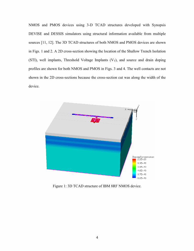
NMOS and PMOS devices using 3-D TCAD structures developed with Synopsis
DEVISE and DESSIS simulators using structural information available from multiple
sources [11, 12]. The 3D TCAD structures of both NMOS and PMOS devices are shown
in Figs. 1 and 2. A 2D cross-section showing the location of the Shallow Trench Isolation
(STI), well implants, Threshold Voltage Implants (VT), and source and drain doping
profiles are shown for both NMOS and PMOS in Figs. 3 and 4. The well contacts are not
shown in the 2D cross-sections because the cross-section cut was along the width of the
device.
Figure 1: 3D TCAD structure of IBM 8RF NMOS device.

5
Figure 2: 3D TCAD structure of IBM 8RF PMOS device.
Figure 3: 2D Cross-section of IBM 8RF NMOS device.

6
Figure 4: 2D Cross-section of IBM 8RF PMOS device.
Table 1: Device properties for the calibrated IBM 8RF NMOS and PMOS devices
Device Property NMOS PMOS
W/L 1 µm/ 130 nm 1 µm/ 130 nm
Gate oxide thickness (tox) 2.5 nm 2.5 nm
Substrate doping 1e16 (Boron)
1e16 (Boron)
Source and Drain doping 2e20 (Arsenic)
2e20 (Boron)
Lightly Doped Drain (LDD) doping 2.5e19 (Arsenic)
2.5e19 (Boron)
Threshold Voltage (VT) Implant 6e18 (Boron)
5e18 (Arsenic)
Deep P-Well 1e18 (Boron) 1e18 (Boron)
Regular N-Well - 1e17 (Arsenic)
Regular P-Well 8e17 (Boron)
-
Shallow Trench Isolation depth 0.36 µm 0.36 µm
Sidewall Doping 5e19 (Boron) 5e19 (Arsenic)

7
Table 1 is a list of the device properties for the calibrated devices. The devices were
calibrated by adjusting the LDD depth, the VT implant, and the depth of the source and
drain doping, to match electrical characteristics (Id-Vg and Id-Vd curves) obtained from
the IBM PDK 130nm compact models. Figures 5 and 6 show a good agreement between
the 3D TCAD calibrated Id-Vg curves and the Id-Vg curves obtained from the IBM 130nm
compact models. Figures 7 and 8 show a good agreement between the 3D TCAD
calibrated Id-Vd curves and the Id-Vd curves obtained from the IBM 130nm compact
models. All simulations were conducted using the ACCRE computing cluster [13].
Figure 5: NMOS IdVg curves of 3D TCAD model vs. IBM 130nm Compact Model
(Vd = 50 mV).

8
Figure 6: PMOS IdVg curves of 3D TCAD model vs. IBM 130nm Compact Model
(Vd = 1.15 V).
Figure 7: NMOS IdVd curves of 3D TCAD model vs. IBM 130nm Compact Model.

9
Figure 8: PMOS IdVd curves of 3D TCAD model vs. IBM 130nm Compact Model.
Effective Collection Depth
A factor that affects the total amount of charge collected is the effective collection
depth [14]. Any track depth that goes beyond the effective collection depth will not result
in additional charge collected at the hit node or at adjacent nodes. Consequently, the
smaller the effective charge collection depth, the smaller the amount of charge collected
by the hit device and adjacent devices.
In order to determine the effective collection depth for both NMOS and PMOS devices,
3-D TCAD simulations were carried out on both NMOS and PMOS devices without the
source, striking the same location and varying the ion-strike depth as shown in Fig. 9.
Absence of the source ensures that the possibility of the parasitic bipolar action turn-on
will not interfere with the charge collected, since the charge collection is strictly a p-n
junction collection.

10
Figure 9: Methodology for measuring effective collection depth, simulation conducted
with ion strikes of varying depths.
In the PMOS device, the n-well/p+-deep-implant-well junction acts as a natural barrier
to charge collection and is located at ~0.9 µm from the surface of the device (see Fig. 4).
As a result, all charge outside the n-well diffuse out, recombine, or are collected by the
substrate contact. Figure 10 shows that for PMOS devices, collected charge increases
linearly until the strike depth of ~0.9 µm beyond which it starts to saturate. The 3-D
TCAD NMOS simulations results shown in Fig. 11 and microbeam experimental data
shown in Fig. 12[15] show the effective collection depth for the NMOS to be ~1.2 µm.
The presence of the retrograde p-well and the p+ implant help limit the charge collection
of the NMOS device [16]. It should be noted that the collected charge for the NMOS
device does not have the sharp onset of saturation that is easily observed in PMOS device

11
and with increase in LET; there is a slight increase in the collection depth. With the
knowledge of the effective collection depth, one can easily calculate the amount of
charge deposited and the LET being used in single event circuit simulations, and the
effective collection depth is useful for performing cross-section calculations.
Figure 10: Simulation results show that the effective collection depth for
PMOS is ~0.9 µm.

12
Figure 11: Simulation results show that the effective collection depth for
NMOS is ~1.2 µm.
Figure 12: Microbeam data shows the collected charge at the drain for 36MeV oxygen
ions (7 MeV/mg/cm2) normally incident to the surface. The active diffusion is bounded
by the dotted lines and extends from 3.5 µm to 13.5µm. From these data, a charge
collection depth of 1 µm was estimated, after Tipton, et al., [15].

13
Parasitic Bipolar Effect
Several basic mechanisms affect charge transport and charge collection after an ion hit
at a circuit node. Much work has been done to estimate the charge collected by a single
junction [1]. The total charge collected is the sum of drift, diffusion, and bipolar
amplification components.
For CMOS technologies, it has been shown that parasitic bipolar action affects the
collected charge [3, 17], and with decreasing gate length, the bipolar current gain
increases [18]. The lateral parasitic bipolar transistor is formed by the drain, channel, and
source region as shown in Figure 13. The drain acts as the collector, the body as the base,
and the source as the emitter for the parasitic bipolar transistor.
Figure 13: The NMOS device has a lateral parasitic npn bipolar transistor; the PMOS
device has a lateral parasitic pnp bipolar transistor.
In simulations, the charge contribution due to bipolar action can be distinguished from
the total charge collection by removing the source (emitter for parasitic bipolar transistor)

14
junction from the simulation, thereby leaving only one p-n junction to collect charge by
drift and diffusion.
To examine the parasitic bipolar effect for this technology node, 3-D TCAD
simulations are conducted for individual PMOS and NMOS devices. The SE simulations
were conducted using devices with and without the source implant (i.e., with and without
the emitter junction for the parasitic bipolar transistor) for the same LET and hit location.
The contacts for the n-well and p-well implants are located at the top of the devices and
are 0.28 µm away from the devices, and the substrate contact was located at the bottom
of the devices. The location of the well contacts represents the minimum parasitic bipolar
amplification because of the reduced resistance for current flow as described by Olson in
[19]. Due to the area of the structure and presence of the p+-deep-implant-well, the
location of the substrate contact has no effect on the parasitic bipolar effect. The
difference in the charge collected at a node with and without the source implant for
individual PMOS and NMOS devices is shown in Fig. 14.
The PMOS device shows high parasitic bipolar amplification compared to the NMOS
device due to a voltage collapse in the n-well during the charge collection process. This
n-well voltage collapse has also been reported by other researchers [19, 20]. Parasitic
bipolar amplification is significant for PMOS devices because the electrons generated
from the ion strike are confined to the n-well region and this in turn drops the n-well
potential, thereby forward biasing the parasitic base-emitter junction and causing the
significant parasitic bipolar amplification. The bipolar amplification is not as significant
in the p-well because the holes can diffuse out over a larger area.
15
Figure 14: Parasitic bipolar transistor effect for individual devices with increase in LET.
Single Event Effects in a 130 nm D Flip-Flop
In order to examine the single event charge collection of the device in situ in the circuit
to properly account for loading effects of complementary devices and capacitance of
adjacent stages, a D Flip-Flop is examined in a mixed-mode simulation. The D flip-flop
is edge-triggered and the output of the Flip-Flop tracks the input when the clock goes
high. The circuit of the D flip-flop circuit is part of DARPA Radiation Hardening By
Design (RHBD) program and is shown in Figure 15 [21]. The unhardened nature of the D
flip-flop makes it susceptible to low LET upsets. Experiments conducted at low LET ions
at Berkeley Laboratory on a shift register made up of an array of D flip-flops showed that
the D flip-flop is very vulnerable to single event upsets as seen in Figure 16 [21]. The
ions used were Argon, Copper, Xenon, and Krypton with LET ranging from 3.45 to 62
MeV/mg/cm2. The angles used for exposure were 0°, 45°, and 60° from normal.

16
Using double exponential, time dependent current pulses described by Massengill in
[1], Spectre simulations were conducted on the IBM 8RF D flip-flop to determine the
devices and nodes most susceptible to upset. The double exponential, time dependent
current pulse used had a rise time of 7 ps and fall time of 200 ps, the peak current was
adjusted accordingly to vary the charge deposited on the node from 1 fC to 100 fC. The
Spectre simulations showed NMOS MN16 (circled in Fig. 15) to be one of the most
sensitive nodes. Next, a 3D TCAD model of MN16 was used in a mixed-mode
simulation. In a mixed-mode simulation, one device is simulated in TCAD (MN16), and
the other devices were electrically connected to the TCAD device and simulated as IBM
PDK 130 nm compact models. The mixed-mode simulation was conducted using an LET
of 3.45 MeV/mg/cm2 at an angle of 60º.

17
Figure 15: Boeing Standard D Flip-Flop for 2005 test chip, the circled device is
the sensitive NMOS device MN16.

18
Also a simulation was conducted using a standalone TCAD transistor connected
directly to the power rail to provide a comparison of the ion strike effects with and
without loading. A comparison of the simulation with and without loading effects shows
that there is a significant difference in the peak currents as seen in Fig. 17. However, Fig.
18 shows that the total amount of charge collected is approximately the same for
simulations with and without loading effects. Also from the mixed-mode simulation it
was determined that the critical charge needed to cause an upset in the D flip-flop is 45
fC as seen in Fig. 18. The waveforms generated from the mixed-mode simulation are
shown in Fig. 19.
Figure 16: D flip-flop cross-section, after Baze, et al., [21].

19
Figure 17: Current pulse for MN16 drain with and without loading effects.
Figure 18: Charge collection for MN16 drain with and without loading effects.

20
Figure 19: Waveforms from the mixed-mode simulation of the D Flip-flop: The state of
the input signal is clocked in and held at the output at every clock rising edge but due to
the ion strike that occur at 36 ns, the output goes low.

21
CHAPTER III
CHARGE SHARING
Introduction
The amount of charge required to represent a logic HIGH state in CMOS digital
circuits has been reduced dramatically with the scaling of supply voltage and nodal
capacitances in semiconductor technology generations, making single events increasingly
problematic. Circuit hardening approaches, such as Triple Mode Redundancy (TMR) [22]
have been employed to address this issue; however many of these techniques are
designed to mitigate effects of charge deposited at a single circuit node. Decreased
spacing of devices with scaling can increase the charge collection at nodes other that than
the hit node [19, 23, and 24]. Such charge collection at multiple nodes due to a single hit
(i.e. “charge sharing”) [25] can render existing methods for SEU mitigation ineffective.
Thus, it is critical to understand the mechanisms and processes that affect the charge
sharing and develop design guidelines that reduce the amount of charge collected at
nodes other than the hit node.
Charge Sharing Mechanisms
It is important to distinguish between the charge that is the direct result of a hit and the
charge that is due to parasitic bipolar action so as to explore an appropriate mitigation
technique. The charge collected due to parasitic bipolar action is specific to the device.
This charge is not shared with adjacent nodes, while charge collected due to
22
drift/diffusion processes is subject to charge sharing with other nodes in proximity.
However, charge transported by diffusion to a secondary device can result in bipolar
amplification if the voltage perturbations on the secondary device are sufficient to turn on
the parasitic bipolar transistor.
Charge sharing takes place due to the diffusion of the carriers in the substrate/well.
Immediately after an ion hit, carriers are collected by drift process due to the electric field
present in the reversed-biased p-n junctions. This is followed by the diffusion of the
carriers from the substrate. For older technologies, the distance between the hit device
and secondary device was large enough that most of the diffusion charge was also
collected by the hit node. However, for advanced technologies, the close proximity of the
devices results in diffusion of charge to nodes other than the hit node. With the very
small amount of charge required to represent a HIGH logic state at a node, the charge
collected due to diffusion at an adjacent node is significant.
The following sections quantify the charge collection between adjacent nodes as a
function of distance to provide layout guidelines for a 130 nm technology.
Simulation Setup
Single event simulations were performed to determine charge collection in the “hit”
device, as well as in other devices in close proximity of the hit device. In the following
discussion, the device that was hit directly by the ion is termed the active device, while
the other device in proximity is termed the passive device. For all simulations, a transistor
size of W/L = 1 µm/130 nm was used. In all simulation results, the charge reported on the
passive device was collected after the passive drain charge-collection saturated. The
23
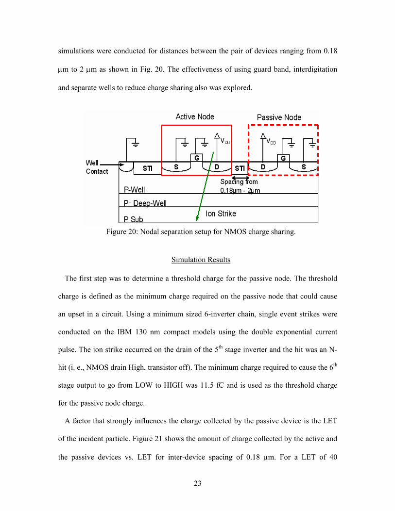
simulations were conducted for distances between the pair of devices ranging from 0.18
µm to 2 µm as shown in Fig. 20. The effectiveness of using guard band, interdigitation
and separate wells to reduce charge sharing also was explored.
Figure 20: Nodal separation setup for NMOS charge sharing.
Simulation Results
The first step was to determine a threshold charge for the passive node. The threshold
charge is defined as the minimum charge required on the passive node that could cause
an upset in a circuit. Using a minimum sized 6-inverter chain, single event strikes were
conducted on the IBM 130 nm compact models using the double exponential current
pulse. The ion strike occurred on the drain of the 5th stage inverter and the hit was an N-
hit (i. e., NMOS drain High, transistor off). The minimum charge required to cause the 6th
stage output to go from LOW to HIGH was 11.5 fC and is used as the threshold charge
for the passive node charge.
A factor that strongly influences the charge collected by the passive device is the LET
of the incident particle. Figure 21 shows the amount of charge collected by the active and
the passive devices vs. LET for inter-device spacing of 0.18 µm. For a LET of 40

24
MeV/mg/cm2, the charge collected by the passive PMOS device is about 40% of the
charge collected by the active PMOS device, compared to the NMOS devices in which
the passive device collects less than 25% of the charge collected by the active device. The
combined total charge collected by the active and the passive nodes as shown in Fig. 21
is 27% higher than the total charge collected by a stand-alone node seen in Fig. 14. This
is due to the parasitic bipolar turn-on and the passive node collection of charge that
would normally diffuse out and recombine.
Figure 21: Charge collection with distance of 0.18 µm between adjacent devices.
The collected charge is also a strong function of the distance between the active and
passive device. Figures 22 and 23 shows the charge collected on the passive node as a
function of distance to the active device. For the PMOS devices, there is very little charge
sharing for spacing greater than 1.62 µm, while the NMOS passive device still collects a
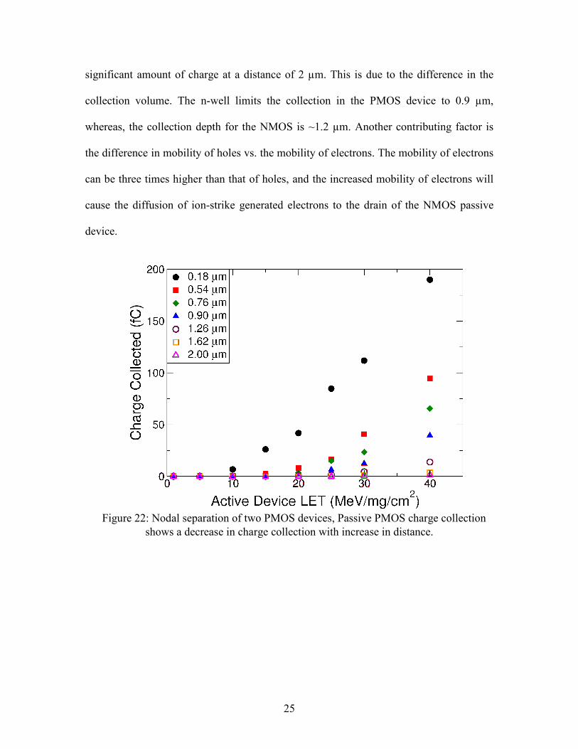
25
significant amount of charge at a distance of 2 µm. This is due to the difference in the
collection volume. The n-well limits the collection in the PMOS device to 0.9 µm,
whereas, the collection depth for the NMOS is ~1.2 µm. Another contributing factor is
the difference in mobility of holes vs. the mobility of electrons. The mobility of electrons
can be three times higher than that of holes, and the increased mobility of electrons will
cause the diffusion of ion-strike generated electrons to the drain of the NMOS passive
device.
Figure 22: Nodal separation of two PMOS devices, Passive PMOS charge collection
shows a decrease in charge collection with increase in distance.

26
Figure 23: Nodal separation of two NMOS devices, Passive NMOS charge collection
shows a decrease in charge collection with increase in distance.
Figure 24 shows the simulation results with the source (emitter for parasitic bipolar)
region from the NMOS and PMOS devices (both active and passive) removed for inter-
device spacing of 0.18 µm. The charge collection decreases significantly for passive
PMOS device when the source is removed, indicating a high contribution from the
parasitic bipolar transistor as seen in Fig. 25. For passive NMOS device, the difference in
charge collection with and without the parasitic bipolar transistor is not significant
because the bipolar effect in the substrate is not as strong as it is inside the n-well. Hence,
the dominant mechanism for charge-sharing in the passive NMOS device is diffusion.

27
Figure 24: Parasitic bipolar amplification effects for Passive devices.
Figure 25: Parasitic bipolar amplification of the drain current in passive PMOS device,
LET = 40 MeV/mg/cm2.

28
In order to determine the charge sharing effect for devices in different wells,
simulations were conducted with inter-device spacing of 0.6 µm between the NMOS and
PMOS device. The devices are interchanged, with the NMOS as the active device and the
PMOS as the passive device, and vice versa. Figure 26 shows that the charge sharing
effect is not as prominent for devices in different wells. The charge collected by the
passive NMOS device at LET of 40 MeV/mg/cm2 is above the threshold, this is due to
the difference in the depth of the n-well located at 0.9 µm and the effective collection
depth of the NMOS transistor at 1.2 µm. It should be noted that with increase in LET, the
charge sharing effect between devices in separate wells is expected to increase as
discussed in [19].
Figure 26: Charge collection for Passive NMOS (PMOS active) and Passive PMOS
(NMOS active).
29
Mitigation Strategies
A solution for mitigating charge sharing is nodal separation. Figures 22 and 23 clearly
show that this is not a practical mitigation technique because the passive node can still
collect 16 fC (which is greater than the charge threshold of 11.5 fC) for a distance of 2
µm between adjacent devices. Due to higher packing densities, there will be several
devices within the 2 µm radius and all of these devices will collect charge due to a single
hit, resulting in multiple SE pulses propagating through the circuit. With technologies
smaller than 130 nm, this problem will become even more severe, requiring hardening
techniques that mitigate multiple SE pulses within the circuit.
As the parasitic bipolar transistor contributes the majority of the collected charge on the
passive PMOS node, hardening approaches should include techniques to reduce overall
contribution of the parasitic bipolar transistor. The main reason parasitic bipolar transistor
turns ON is the collapse of the well voltage, which forward biases the parasitic transistor
base-emitter junction. Additional well contacts or guard band around each transistor in
the well will prevent the well voltage from collapsing, thereby decreasing the
contribution by the parasitic bipolar transistor. The presence of the guard-band causes an
increase of 30% in the area compared to the minimum nodal separation of 0.18 µm
between the transistors. Figures 27 and 28 show the charge collection on the passive
device with and without a guard ring around the active devices. At an LET of 40
MeV/mg/cm2, the passive PMOS device collects 97% less charge than without the guard
ring, whereas the NMOS passive device collects 35% less charge.
The significant decrease in the amount of charge collected by the PMOS passive device
is due to the guard ring which helps maintain the well potential, and prevents the parasitic

30
bipolar transistor from turning on. The guard-band mitigation technique is marginally
effective in the NMOS charge sharing because the primary charge-sharing mechanism is
diffusion and not the parasitic bipolar transistor turn-on.
Figure 27: The contacted guard-band is highly effective in mitigating PMOS
charge sharing.
31
Figure 28: The contacted guard-band is marginally effective in mitigating NMOS
charge sharing.
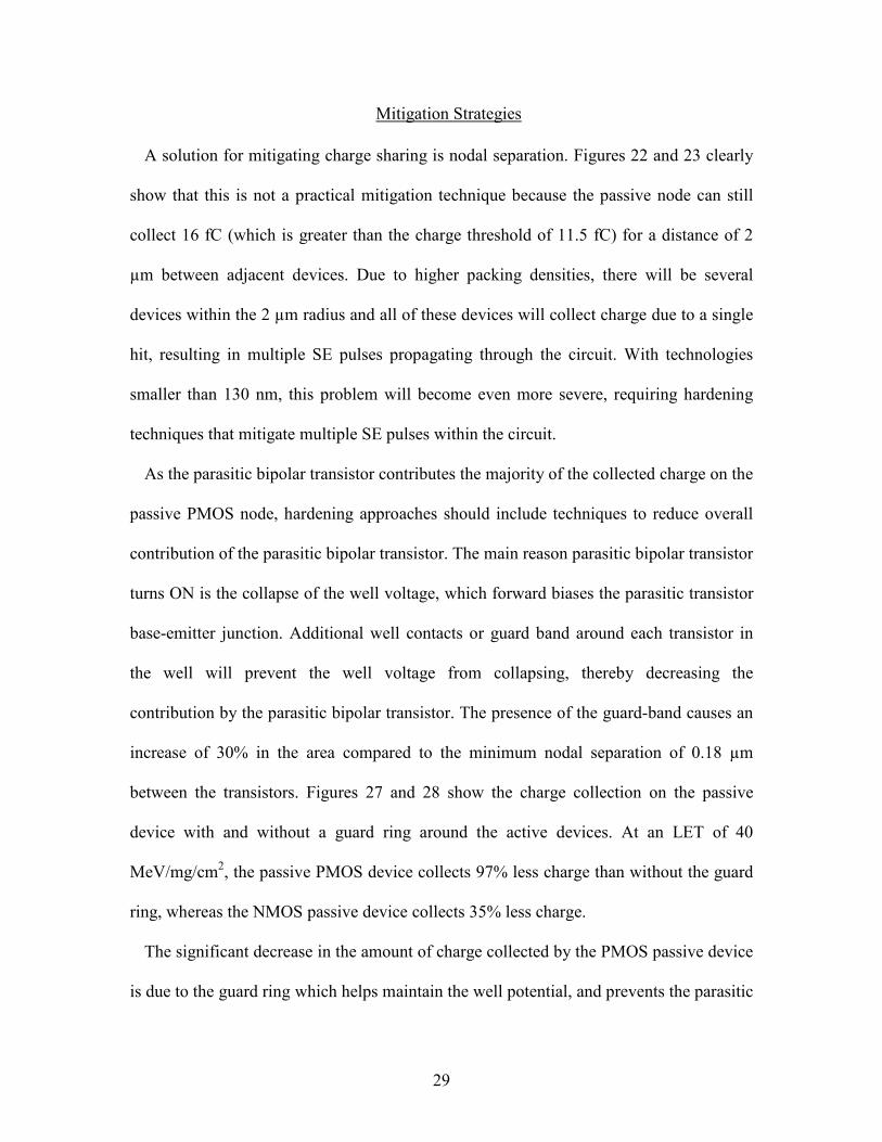
Another mitigation technique considered for PMOS charge sharing is the use of
separate wells as shown in Figure 29. It should be noted that the use of separate wells will
consume more area than using a contacted guard band, however for this simulation, the
device spacing between the three different scenarios presented in Fig. 30 is 1.52 µm.
Figure 30 shows that the use of the contacted guard band is more effective than using
separate wells.

32
Figure 29: Active PMOS and Passive PMOS devices separated by a P-Well
Figure 30: The use of contacted guard-band for PMOS charge sharing is more effective
compared to the use of separate wells.
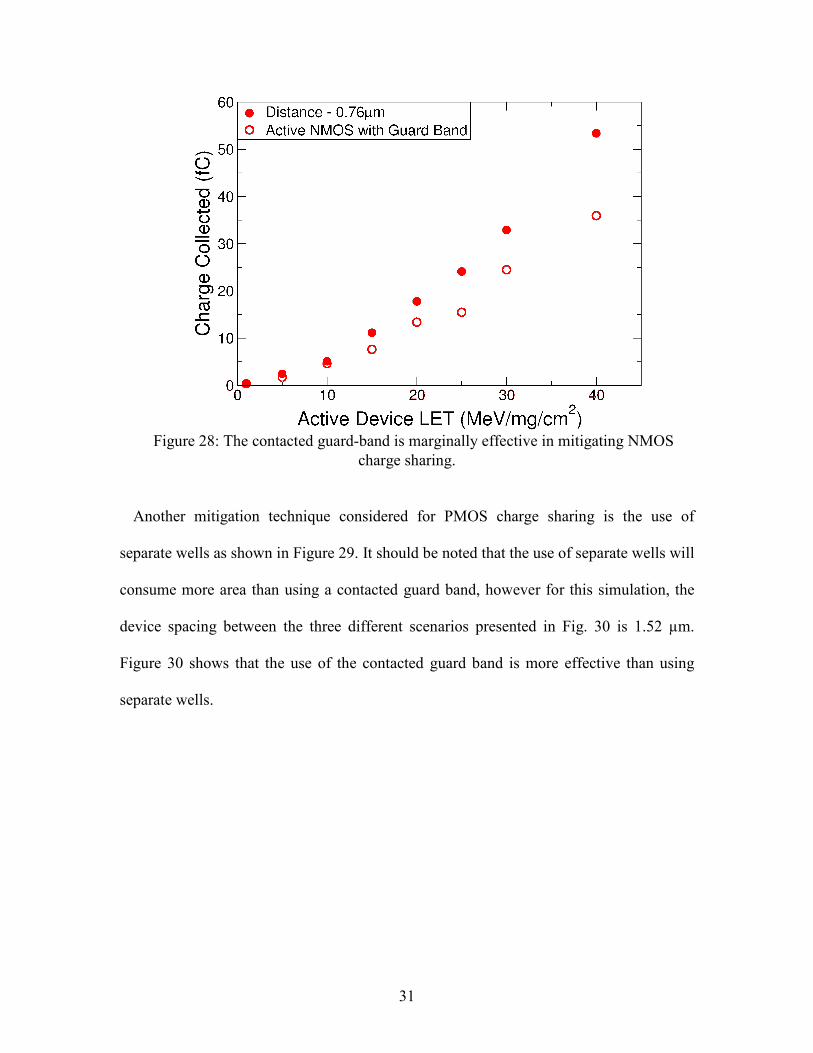
For NMOS charge sharing, interdigitating the transistors is considered as shown in Fig.
31. The less-sensitive node can be a transistor in the same combinational logic circuit as
the active and passive devices or a transistor from another combinational logic circuit.
33
Here it is assumed that the less-sensitive node is less vulnerable to SE strikes as
compared to the passive node, therefore the increase in the charge collection on the less-
sensitive node is less likely to cause an upset. Figure 32 shows that the use of
interdigitation can be effective for NMOS charge sharing, provided that the layout
designer has a previous knowledge of the sensitivity and vulnerability of each node in the
cell to SE strikes.
Figure 31: Interdigitation to mitigate NMOS charge sharing

34
Figure 32: The less-sensitive node collects most of the diffusion charge, thereby
reducing the passive node charge collection.
Conclusion
Charge sharing between two devices in the same well was simulated for the IBM 8RF
(twin well option) 130 nm technology. For the PMOS devices, the parasitic bipolar
significantly increases the total charge collected by the passive (non-hit) node, while the
main mechanism for charge sharing in the NMOS devices is diffusion. Due to scaling
trends, (i.e., higher packing densities and lower nodal capacitances), both parasitic
bipolar amplification and charge diffusion are expected to be exacerbated, thereby
making charge sharing a major SE issue in future technologies.
Contacted guard-band reduced the charge sharing between PMOS devices in the n-well
by 97% and between NMOS devices in the p-well by 35%. Therefore, the most effective
mitigation technique for PMOS charge sharing mitigation is the use of contacted guard-
band because it eliminates the drop in the n-well potential that allows the parasitic bipolar
to turn on. For NMOS charge sharing, a combination of nodal separation, interdigitation,
and contacted guard-band should help mitigate the charge sharing effect.
35
CHAPTER IV
SINGLE EVENT EFFECTS IN A 130 nm DICE LATCH
Introduction
Critical charge to maintain a logic HIGH is steadily decreasing with decreasing feature
size. Many methods have been developed to increase critical charge requirement for
storage elements, thereby reducing the error rates [22, 26, and 27]. Design-based
approaches have been proposed that use four storage nodes instead of two nodes to retain
data [5]. Such designs are considered SEU immune at low LET ion hits for all practical
purposes because a single ion hit at a storage node does not cause an upset. However,
such designs are vulnerable to hits that deposit charge on multiple nodes [23]. Since,
multiple node hits are very rare, such designs were considered practically SEU immune.
However, for deep sub-micron technologies, the proximity of circuit nodes results in
charge collection at multiple nodes when a single ion strikes a node. Researchers first
observed the effect of such charge sharing in hardened SRAM designs [23]. Experimental
data showing upsets in DICE latch design when exposed to low LET ions was
unexpected based on the assumed hardness of the circuit. Circuit and 3D TCAD
simulations show that charge sharing between sensitive pairs of devices as the primary
reason for upsets.

36
DICE Design and SEU Exposure
Figure 33: Master stage of DICE cell
The DICE cell design has a master and slave stage, the master stage is shown in Fig.
33. A test chip utilizing an array of these latches was designed in a shift register fashion
and fabricated in the IBM 8RF 130 nm CMOS technology as part of the DARPA RHBD
program [21]. Multiple shift registers were put in parallel to isolate clock hits from
individual node hits in a DICE cell (clock line hits will result in upsets for all shift
registers, individual hits will result in upsets in a single shift register). This design was

37
exposed to low LET ions at Berkeley Laboratory. The ions used were Argon, Copper,
Xenon, and Krypton with LET ranging from 3.45 to 62 MeV/mg/cm2. The angles used
for exposure were 0°, 45°, and 60° from normal. Due to hardened nature of DICE cell
and low LET of particles, no upsets were expected except at very high LETs. However,
Fig. 34 [21] shows that the DICE cell upsets for LETs as low as 13.77 MeV/mg/cm2.
These upsets were consistent through out the experiments and unexpected as a single low
LET ion hits on a node can not cause an upset in a DICE latch. Charge sharing between
two nodes due to one ion hit was proposed as the main reason for upset. This theory was
verified through circuit and 3D TCAD simulations as described in the following section.
Figure 34: Data shows DICE upsets at LET values well below theoretical expectations,
after Baze, et al, [21]

38
Circuit and 3D TCAD Simulation Approach
An exhaustive set of single node hit circuit-level simulations were conducted on
the 130 nm DICE latch using Cadence Spectre circuit simulator to confirm that single
node hit will not cause an upset for the DICE latch [28]. The simulations were conducted
using the double-exponential current pulse described in [1]. The double exponential, time
dependent current pulse used had a rise time of 7 ps and fall time of 200 ps, the peak
current was adjusted accordingly to vary the charge deposited on the node from 1 fC to 1
pC. The simulation results from the single node hit confirmed the hardness of the DICE
latch to single node hit upsets. Charge sharing between two nodes does not necessarily
affect the DICE circuit operation. Only when charge is collected by specific pairs of
sensitive nodes, the circuit operation may be disrupted. Sensitive pairs are defined as two
transistors that upon simultaneous charge collection cause the DICE latch to upset. The
double exponential current pulse was used to inject charge at the drain of the sensitive
pairs. The double exponential, time dependent current pulse used had a rise time of 7 ps
and fall time of 200 ps, the peak current was adjusted accordingly to vary the charge
deposited on the nodes from 1 fC to 100 fC. An exhaustive set of circuit simulations were
performed in order to determine sensitive pairs for the DICE latch circuit shown in Figure
33. The circuit simulations accounted for the four possible input states:
• when data is high and clock is high
• when data is high and clock is low
• when data is low and clock is high
• when data is low and clock is low
The DICE latch design consisted of 66 transistors which resulted in 4356 node
39
pairs for each input state. As charge sharing is a strong function of layout, and layout may
contain any of these nodes in close proximity, all possible combinations of node pairs
were simulated. The circuit simulations identified a total of 124 unique pairs of sensitive
nodes; 48 of which are PMOS-NMOS pairs, 56 are PMOS-PMOS pairs, and 20 are
NMOS-NMOS pairs as seen in Table 2 [28]. These sensitive pairs are due to the circuit
function and are independent of the layout of the DICE latch.

40
Table 2
List of Sensitive Node Pairs for DICE latch. D=Data. C=Clock.
D high, C high D high, C low D low, C high D low, C low
MN30 MN32 MN10 MN13 MN18 MN25 MN3 MN6
MP18 MN32 MN10 MN14 MN18 MN26 MP10 MN6
MP18 MP25 MN10 MN16 MN18 MN28 MP10 MP13
MP18 MP26 MN11 MN13 MN19 MN25 MP10 MP14
MP18 MP27 MN11 MN14 MN19 MN26 MP10 MP15
MP18 MP28 MN11 MN16 MN19 MN28 MP10 MP16
MP18 MP29 MN8 MN13 MN21 MN25 MP10 MP17
MP19 MN32 MN8 MN14 MN21 MN26 MP11 MN6
MP19 MP25 MN8 MN16 MN21 MN28 MP11 MP13
MP19 MP26 MP3 MN10 MP30 MN18 MP11 MP14
MP19 MP27 MP3 MN11 MP30 MN19 MP11 MP15
MP19 MP28 MP3 MN8 MP30 MN21 MP11 MP16
MP20 MN32 MP3 MN9 MP30 MP32 MP11 MP17
MP20 MP25 MP3 MP6 MP30 MP33 MP12 MN6
MP20 MP26 MP3 MP7 MP31 MN18 MP12 MP13
MP20 MP27 MP4 MN10 MP31 MN19 MP12 MP14
MP20 MP28 MP4 MN11 MP31 MN21 MP12 MP15
MP20 MP29 MP4 MN8 MP31 MP32 MP12 MP16
MP21 MN32 MP4 MN9 MP31 MP33 MP12 MP17
MP21 MP25 MP4 MP6 MP32 MN25 MP13 MN3
MP21 MP26 MP4 MP7 MP32 MN26 MP14 MN3
MP21 MP27 MP6 MN13 MP32 MN28 MP15 MN3
MP21 MP28 MP6 MN14 MP33 MN25 MP16 MN3
MP21 MP29 MP6 MN16 MP33 MN26 MP17 MN3
MP22 MN32 MP6 MN17 MP33 MN28 MP8 MN6
MP22 MP25 MP7 MN13 MP8 MP13
MP22 MP26 MP7 MN14 MP8 MP14
MP22 MP27 MP7 MN16 MP8 MP15
MP22 MP28 MP7 MN17 MP8 MP16
MP22 MP29 MP8 MP17
MP25 MN30 MP9 MN6
MP26 MN30 MP9 MP13
MP27 MN30 MP9 MP15
MP28 MN30 MP9 MP16
MP29 MN30 MP9 MP17

41
Of all the possible combinations of sensitive pairs, only some of the pairs are in close
proximity to each other on a layout. All sensitive pairs were examined in the DICE latch
layout to identify pairs that have the least distance between the nodes. Based on the
distance between the sensitive pairs, three pairs were identified as the case-study
examples and considered for further analysis. The pairs included: MN18 and MN28
shown in Fig. 35 with the distance of 1.41 µm between the devices. This pair of devices
was sensitive when data was low and clock was high. MP22 and MP28 with distance of
0.74 µm between devices shown in Fig. 36 were sensitive when both data and clock are
high; and MP25 and MN30 with distance of 4.3 µm between devices shown in Fig. 37
were sensitive when both data and clock are high.
Figure 35: An excerpt showing layout proximity of sensitive NMOS-NMOS node pair
MN28-MN18 in the DICE layout.

42
Figure 36: An excerpt showing layout proximity of sensitive PMOS-PMOS node pair
MP22-MP28 in the DICE layout.
Figure 37: An excerpt showing layout proximity of sensitive NMOS-PMOS node pair
MN30-MP25 in the DICE layout.
Once the case-study sensitive pairs were identified, the next step was to determine the
amount of charge needed on each of the two nodes to cause an upset in the DICE latch.
This was done using exponential current sources to model charge collection process at
each node in a Spectre simulation. The device that was hit directly by the ion is termed
the active device, while the other device in proximity is termed the passive device. The
double exponential, time dependent current pulse used had a rise time of 7 ps and fall
time of 200 ps, the peak current was adjusted accordingly to vary the charge deposited on

43
the active and passive nodes for each sensitive pair from 1 fC to 100 fC in 1 fC
increments [28]. The charge contours in Figs. 38, 39, and 40 [28] show an upset region
with the amount of charge needed on each transistor to cause an upset in the DICE latch.
It should be noted that the charge contours are an approximation due to the use of a
constant pulse width for the varied charge depositions.
Figure 38: Upset/No-Upset SHMOO plot for each sensitive NMOS pair quantifies the
charge sharing necessary for upset, after Sternberg, [28].

44
Figure 39: Upset/No-Upset SHMOO plot for each sensitive PMOS pair quantifies the
charge sharing necessary for upset, after Sternberg, [28].
Figure 40: Upset/No-Upset SHMOO plot for each sensitive NMOS-PMOS pair
quantifies the charge sharing necessary for upset, after Sternberg, [28].
Upset Region
Upset Region

45
Next, a calibrated 3D TCAD model was used to determine if two sensitive nodes
collected enough charge to cause an upset for a given LET and angle of incidence. Both
the active and the passive devices were included in the 3D model with actual physical
dimensions being the same as that on the layout as shown in Figs. 41, 42, and 43. The
devices are simulated in the OFF state, the active device was struck using different LET
values, and the resulting charge collection at both device nodes was monitored. Current
pulses at both the active and passive nodes were integrated to obtain the total amount of
charge collected by each node. Simulations were carried out not only for normal strikes,
but also for 45° and 60° angle strikes. The angles used were selected such that the ion
would pass under the passive device to yield a worst-case scenario estimate.
Figure 41: 3D TCAD layout of simulated NMOS-NMOS node pair MN28-MN18.

46
Figure 42: 3D TCAD layout of simulated PMOS-PMOS node pair MP22-MP28
Figure 43: 3D TCAD layout of simulated PMOS-NMOS node pair MP25-MN30

47
The tables below show the results for these simulations. Each table section is for a pair
of sensitive nodes. The role of active and passive was reversed for the pair comprised of
MP25 (PMOS) and MN30 (NMOS) with the results shown in the tables 5 and 6.
Table 3: Results for NMOS Pair (MN18 and MN28)
LET/Angle and total amount of charge collected (fC)
Qcrit
(fC) 9.74/60º 21.33/0º 21.33/60º 31.3/0º 31.3/45º
MN18 Active 15 48 221 110 333 227
MN28 Passive 18 35 9 81 14 93
Table 4: Results for PMOS Pair (MP22 and MP28)
LET/Angle and total amount of charge collected (fC)
Qcrit
(fC) 9.74/60º 21.33/0º 21.33/60º 31.3/0º 31.3/45º
MP28 Active 15 106 474 378 779 484
MP22 Passive 16 118 42 254 119 254
Table 5: Results for NMOS/PMOS Pair (MN30 and MP25)
LET/Angle and total amount of charge collected (fC)
Qcrit
(fC) 9.74/60º 21.33/0º 21.33/60º 31.3/0º 31.3/45º
MN30 Active 5 73 229 172 337 344
MP25 Passive 12 0 0 16 0 0

48
Table 6: Results for PMOS/NMOS Pair (MP25 and MN30)
LET/Angle and total amount of charge collected (fC)
Qcrit
(fC) 9.74/60º 21.33/0º 21.33/60º 31.3/0º 31.3/45º
MP25 Active 12 188 339 468 546 668
MN30 Passive 5 0 0 2 0 0
Results indicate that charge sharing occurs more readily between devices in the same
wells (i.e., from PMOS to PMOS and NMOS to NMOS) as shown in Tables 3 and 4,
with very little charge sharing occurring across a well boundary (i.e. between PMOS and
NMOS), as shown in Tables 5 and 6.
The next set of simulations conducted were 3D mixed-mode simulations with the
sensitive pairs in 3D TCAD and the rest of the DICE cell in IBM 130 nm compact
models. This was done to account for loading effects and to simulate a worst case
scenario, the angled strikes were angled towards the passive device. For each case-study
example examined, the strike occurs when the sensitive pair can cause an upset based on
the state of the Data and Clock as seen in Table 2. Table 7 shows the mixed-mode
sensitive pair upsets versus upsets seen in the experiment data. These 3D mixed-mode
simulations clearly show that low LET particles may cause enough charge collection at
sensitive node pairs to cause an upset. Such charge sharing effects not only affect the
DICE latches, but will affect combinational logic as well.

49
Table 7: 3D mixed-mode simulation upsets vs. Heavy ion data.
3D mixed-mode simulation
LET/Angle
Heavy ion
data
NMOS Pair
MN28/MN18
PMOS Pair
MP28/MP22
NMOS/PMOS Pair
MP25/MN30
9.74/45° Upset No Upset No Upset No Upset
9.74/60° Upset No Upset Upset No Upset
21.33/0° Upset No Upset No Upset No Upset
21.33/60° Upset Upset Upset No Upset
31.3/0° Upset No Upset Upset No Upset
31.3/45° Upset Upset Upset No Upset
Conclusion
Experimental results clearly show that a hardened cell (DICE) is vulnerable to SEU at
low LET. This vulnerability is shown to be due to charge sharing between a hit node and
an adjacent node in proximity. 3D TCAD standalone simulations show that the charge
sharing effect is more pronounced for devices in the same well, and not as significant for
devices in separate wells. Mixed-mode simulations show that the DICE will upset due to
charge sharing as seen in the experimental data. The use of careful design layout
(separating sensitive pairs in the layout design) can help increase the SE hardness of this
cell and other cells in a given design library.
50
CHAPTER V
CONCLUSION
In this work, we have investigated the single event effects for the IBM 8RF 130 nm
CMOS technology through a combination of circuit and 3D TCAD simulations, and have
verified the simulation results with experimental data.
Modeling and calibration of the 130 nm allowed for a full analysis of the charge
collection and charge sharing properties for this technology node. For charge collection,
the presence of a n+/p+ junction in the PMOS and a deep p+ implant in the NMOS
helped reduce the total amount of charge collected from an ion strike due to the reduced
collection depth. The reduction in the total charge collected not only affects the struck
device but also the devices in proximity.
Due to the reduced gate length, the turn-on the parasitic bipolar transistor is significant
even at low LETs. This parasitic bipolar amplification is more pronounced in the PMOS
devices than the NMOS devices because of the n-well voltage perturbation that occurs
after an ion strike due to the confinement of the ion-strike generated electrons to the n-
well region.
Using a D flip-flop, the critical charge needed to cause an upset and the associated
current pulse for this technology were determined through a mixed-mode simulation. The
simulation results were corroborated by the heavy ion experimental data and showed the
accuracy of the calibrated 3D models. Also, it demonstrates the effectiveness of using 3D
TCAD mixed-mode simulations to not only predict device response to single events, but

51
also to help guide heavy ion experiments.
Charge sharing effects between adjacent devices have been examined and quantified.
Due to scaling trends (i.e. reduced spacing and decrease in nodal capacitance), charge
sharing for deep-submicron technologies will be a major SE issue. Devices in the same
well are more prone to charge sharing than device in separate wells. In terms of
mitigation, PMOS charge sharing can be mitigated effectively by using contacted guard-
ring. The presence of the guard-ring helps maintain the nwell potential thereby reducing
the parasitic bipolar effect which is the primary effect for PMOS charge sharing. On the
other hand, NMOS charge sharing can only be mitigated through a combination of
interdigitation, contacted guard-rings, and nodal separation because the primary
mechanism is diffusion.
A DICE latch is an example of a RHBD circuit, and requires a multiple node hit to
cause an upset. However, due to charge sharing, experimental data and mixed-mode
simulation results show the DICE latch to be vulnerable to low LET ions. This charge
sharing effect will affect other circuit hardening techniques because most of the circuit
level hardening techniques is based on the assumption that charge is collected at a single
node. The DICE latch and other circuit hardening techniques can retain their hardness
through layout mitigation techniques that include contacted guard-ring, interdigitation,
and nodal separation.

52
Appendix
Devise file for NMOS devise
;This file contains the structural dimensions ,the doping profiles and the meshing for the
;calibrated ;IBM 8RF NMOS device
(isegeo:set-default-boolean "ABA")
;Bulk
(isegeo:create-cuboid (position -1.21 2 5) (position 3.5 -2 0) "Silicon" "R.Bulk")
;Gate poly and oxide
(isegeo:create-cuboid (position 1.205 0.4 0) (position 1.085 -0.6 -0.0025) "SiO2"
"R.GateOxide")
(isegeo:create-cuboid (position 1.205 0.4 -0.0025) (position 1.085 -0.6 -0.1425)
"PolySi" "R.PolyGate")
;Field oxide extensions
(isegeo:create-cuboid (position 1.205 0.4 -0.0) (position 1.085 0.63 -0.025) "SiO2"
"R.FieldOxideA")
(isegeo:create-cuboid (position 1.205 -0.6 -0.0) (position 1.085 -0.83 -0.025) "SiO2"
"R.FieldOxideB")
;Gate poly extensions
(isegeo:create-cuboid (position 1.205 0.4 -0.025) (position 1.085 0.63 -0.1425) "PolySi"
"R.PolyGateA")
(isegeo:create-cuboid (position 1.205 -0.6 -0.025) (position 1.085 -0.83 -0.1425) "PolySi"

53
"R.PolyGateB")
;STI
(isegeo:create-cuboid (position 3.5 0.4 0) (position 1.59 -0.6 0.36) "SiO2" "R.STI2")
(isegeo:create-cuboid (position -1.21 0.77 0) (position 3.5 0.4 0.36) "SiO2"
"R.STI3")
(isegeo:create-cuboid (position -1.21 1.05 0) (position 3.5 2 0.36) "SiO2" "R.STI4")
(isegeo:create-cuboid (position 0.7 0.4 0) (position -1.21 -0.6 0.36) "SiO2" "R.STI6")
(isegeo:create-cuboid (position -1.21 -0.4 0) (position 0 -2 0.36) "SiO2"
"R.STI7")
(isegeo:create-cuboid (position 3.5 -0.6 0) (position 0 -2 0.36) "SiO2" "R.STI8")
(isegeo:create-cuboid (position -1.21 0.77 0) (position 0.29 1.05 0.36) "SiO2"
"R.STI9")
(isegeo:create-cuboid (position 3.5 0.77 0) (position 2 1.05 0.36) "SiO2" "R.STI10")
;;Contacts
(isegeo:define-contact-set "Drain" 4.0 (color:rgb 1.0 1.0 0.0 ) "##")
(isegeo:define-contact-set "Gate" 4.0 (color:rgb 1.0 0.0 1.0 ) "##")
(isegeo:define-contact-set "Source" 4.0 (color:rgb 1.0 1.0 1.0 ) "##")
(isegeo:define-contact-set "Substrate" 4.0 (color:rgb 0.0 1.0 1.0 ) "##")
(isegeo:define-contact-set "Pwell" 4.0 (color:rgb 0.0 1.0 1.0 ) "##")
(isegeo:create-cuboid (position 1.205 0.4 -0.1425) (position 1.085 -0.6 -2) "Metal"
"Gatemetal")
(isegeo:define-3d-contact (find-face-id (position 1.145 0 -0.1425)) "Gate")
(isegeo:delete-region (find-body-id (position 1.145 0 -1)))

54
(isegeo:create-cuboid (position 0.59 1 0) (position 1.7 0.82 -2) "Metal" "Pwellmetal")
(isegeo:define-3d-contact (find-face-id (position 0.8 0.92 0)) "Pwell")
(isegeo:delete-region (find-body-id (position 0.8 0.92 -1)))
(isegeo:define-3d-contact (find-face-id (position 0 0 5)) "Substrate")
(isegeo:create-cuboid (position 1.4975 0.3 0) (position 1.2975 -0.5 -2) "Metal"
"Sourcemetal")
(isegeo:define-3d-contact (find-face-id (position 1.3975 0 0)) "Source")
(isegeo:delete-region (find-body-id (position 1.3975 0 -1)))
(isegeo:create-cuboid (position 0.9925 0.3 0) (position 0.7925 -0.5 -2) "Metal"
"Drainmetal")
(isegeo:define-3d-contact (find-face-id (position 0.8925 0 0)) "Drain")
(isegeo:delete-region (find-body-id (position 0.8925 0 -1)))
;------------- Lets add in some dopings for the device --------------------------------------------
;----- First, lets begin with all the constant doping profiles
;Constant Doping in the poly
(isedr:define-constant-profile "Profile.Polyconst.Phos" "ArsenicActiveConcentration"
1e20)
(isedr:define-constant-profile-material "Place.Polyconst.Phos1" "Profile.Polyconst.Phos"
"PolySi")

55
;-- Constant Doping in the silicon substrate region
(isedr:define-refinement-window "Window.Silconst.Bor" "Cuboid" (position -1.21 2 0)
(position 3.5 -2 5))
(isedr:define-constant-profile "Profile.Silconst.Bor" "BoronActiveConcentration" 1e16)
(isedr:define-constant-profile-placement "Place.Silconst.Bor" "Profile.Silconst.Bor"
"Window.Silconst.Bor")
;-- Boron doping in the silicon
;-- Assumes deep pwell implant goes through whole die
(isedr:define-refinement-window "Window.DeepPWell.Bor.1" "Rectangle" (position -
1.21 2 1.25) (position 3.5 -2 1.25))
(isedr:define-gaussian-profile "Profile.DeepPWell.Bor.1" "BoronActiveConcentration"
"PeakPos" 0 "PeakVal" 1e18 "ValueAtDepth" 1e16 "Depth" 0.4 "Gauss" "Factor"
0.0001)
(isedr:define-analytical-profile-placement "Place.DeepPWell.Bor.1"
"Profile.DeepPWell.Bor.1" "Window.DeepPWell.Bor.1" "Symm" "NoReplace" "Eval")
; Regular pwell
(isedr:define-refinement-window "Window.PWell.Bor.2" "Rectangle" (position -1.21 2
0.65) (position 3.5 -2 0.65))
(isedr:define-gaussian-profile "Profile.PWell.Bor.2" "BoronActiveConcentration"
"PeakPos" 0 "PeakVal" 8e17 "ValueAtDepth" 1e17 "Depth" 0.35 "Gauss" "Factor" 0.01)
(isedr:define-analytical-profile-placement "Place.PWell.Bor.2" "Profile.PWell.Bor.2"
"Window.PWell.Bor.2" "Symm" "NoReplace" "Eval")

56
;pwell contact doping
(isedr:define-refinement-window "Window.PWellCon.Bor.3A" "Rectangle" (position
0.29 1.05 0) (position 2 0.77 0))
(isedr:define-gaussian-profile "Profile.PWellCon.Bor.3A" "BoronActiveConcentration"
"PeakPos" 0 "PeakVal" 9e19 "ValueAtDepth" 1e17 "Depth" 0.08 "Gauss" "Factor" 0.01)
(isedr:define-analytical-profile-placement "Place.PWellCon.Bor.3A"
"Profile.PWellCon.Bor.3A" "Window.PWellCon.Bor.3A" "Symm" "NoReplace" "Eval")
; STI Implant - Front & Back Extensions (Added 4/06/06)
(isedr:define-refinement-window "Window.FrontB" "Cuboid" (position 1.205 0.4 0)
(position 1.085 0.385 0.36))
(isedr:define-refinement-window "Window.BackB" "Cuboid" (position 1.205 -0.6 0)
(position 1.085 -0.585 0.36))
(isedr:define-constant-profile "Profile.ImplantB" "BoronActiveConcentration" 5e19)
(isedr:define-constant-profile-placement "Place.Implant.FrontB" "Profile.ImplantB"
"Window.FrontB")
(isedr:define-constant-profile-placement "Place.Implant.BackB" "Profile.ImplantB"
"Window.BackB")
;-- Arsenic doping in the silicon
; - DRAIN SIDE
(isedr:define-refinement-window "drain.Profile.Region" "Rectangle" (position 1.056 0.4
0) (position 0.7 -0.6 0))
(isedr:define-gaussian-profile "drain.Profile" "ArsenicActiveConcentration" "PeakPos" 0
"PeakVal" 2e20 "ValueAtDepth" 1e17 "Depth" 0.08 "Gauss" "Factor" 0.1)

57
(isedr:define-analytical-profile-placement "drain.Profile.Place" "drain.Profile"
"drain.Profile.Region" "Symm" "NoReplace" "Eval")
; - SOURCE SIDE
(isedr:define-refinement-window "source.Profile.Region" "Rectangle" (position 1.234 0.4
0) (position 1.59 -0.6 0))
(isedr:define-gaussian-profile "source.Profile" "ArsenicActiveConcentration" "PeakPos"
0 "PeakVal" 2e20 "ValueAtDepth" 1e17 "Depth" 0.08 "Gauss" "Factor" 0.1)
(isedr:define-analytical-profile-placement "source.Profile.Place" "source.Profile"
"source.Profile.Region" "Symm" "NoReplace" "Eval")
; Lightly Doped Drain
(isedr:define-refinement-window "drainldd.Profile.Region" "Rectangle" (position (-
1.106 0.0) 0.4 0) (position 0.7 -0.6 0))
(isedr:define-gaussian-profile "drainldd.Profile" "ArsenicActiveConcentration"
"PeakPos" 0 "PeakVal" 2.5e19 "ValueAtDepth" 1e17 "Depth" 0.03 "Gauss" "Factor" 0.1)
(isedr:define-analytical-profile-placement "drainldd.Profile.Place" "drainldd.Profile"
"drainldd.Profile.Region" "Symm" "NoReplace" "Eval")
; Lightly Doped Source
(isedr:define-refinement-window "sourceldd.Profile.Region" "Rectangle" (position (+
1.184 0.0) 0.4 0) (position 1.59 -0.6 0))
(isedr:define-gaussian-profile "sourceldd.Profile" "ArsenicActiveConcentration"
"PeakPos" 0 "PeakVal" 2.5e19 "ValueAtDepth" 1e17 "Depth" 0.03 "Gauss" "Factor" 0.1)
(isedr:define-analytical-profile-placement "sourceldd.Profile.Place" "sourceldd.Profile"
"sourceldd.Profile.Region" "Symm" "NoReplace" "Eval")

58
; Vt IMPLANT
(isedr:define-refinement-window "implant.Profile.Region" "Rectangle" (position 1.175
0.4 0.0165) (position 1.115 -0.6 0.0165))
(isedr:define-gaussian-profile "implant.Profile" "BoronActiveConcentration" "PeakPos"
0 "PeakVal" 6e18 "ValueAtDepth" 1e17 "Depth" 0.0165 "Gauss" "Factor" 0.0001)
(isedr:define-analytical-profile-placement "implant.Profile.Place" "implant.Profile"
"implant.Profile.Region" "Symm" "NoReplace" "Eval")
;;bulk meshing
; Meshing Strategy:
(isedr:define-refinement-size "size.whole" 0.25 0.3 0.25 0.1 0.1 0.05)
(isedr:define-refinement-window "window.whole" "Cuboid" (position -1.21 2 0)
(position 3.5 -2 5))
(isedr:define-refinement-placement "placement.whole" "size.whole" "window.whole" )
(isedr:define-refinement-size "size.well" 0.1 0.1 0.05 0.05 0.05 0.05)
(isedr:define-refinement-function "size.well" "DopingConcentration" "MaxTransDiff" 1)
(isedr:define-refinement-window "window.well" "Cuboid" (position 0.29 0.77 0)
(position 2 1.05 0.1))
(isedr:define-refinement-placement "placement.well" "size.well" "window.well" )
(isedr:define-refinement-size "size.dopingmesh1" 0.1 0.1 0.05 0.025 0.025 0.025)
(isedr:define-refinement-function "size.dopingmesh1" "DopingConcentration"
"MaxTransDiff" 1)
(isedr:define-refinement-window "window.dopingmesh1" "Cuboid" (position 0.7 0.4 0)
(position 1.59 -0.6 0.1))

59
(isedr:define-refinement-placement "placement.dopingmesh1" "size.dopingmesh1"
"window.dopingmesh1" )
(isedr:define-refinement-size "size.dopingmesh2" 0.075 0.075 0.05 0.005 0.01 0.005)
(isedr:define-refinement-function "size.dopingmesh2" "DopingConcentration"
"MaxTransDiff" 1)
(isedr:define-refinement-window "window.dopingmesh2" "Cuboid" (position 1.215 0.4
0) (position 1.075 -0.6 0.1))
(isedr:define-refinement-placement "placement.dopingmesh2" "size.dopingmesh2"
"window.dopingmesh2" )
(ise:save-model "NMOS")

60
Devise file for PMOS devise
;This file contains the structural dimensions ,the doping profiles and the meshing for the
;calibrated ;IBM 8RF PMOS device
(isegeo:set-default-boolean "ABA")
;Bulk
(isegeo:create-cuboid (position -1.21 2 5) (position 3.5 -2 0) "Silicon" "R.Bulk")
;Gate poly and oxide
(isegeo:create-cuboid (position 1.205 0.4 0) (position 1.085 -0.6 -0.0025) "SiO2"
"R.GateOxide")
(isegeo:create-cuboid (position 1.205 0.4 -0.0025) (position 1.085 -0.6 -0.1425)
"PolySi" "R.PolyGate")
;Field oxide extensions
(isegeo:create-cuboid (position 1.205 0.4 0.0) (position 1.085 0.63 -0.025) "SiO2"
"R.FieldOxideA")
(isegeo:create-cuboid (position 1.205 -0.6 0.0) (position 1.085 -0.83 -0.025) "SiO2"
"R.FieldOxideB")
;Gate poly extensions
(isegeo:create-cuboid (position 1.205 0.4 -0.025) (position 1.085 0.63 -0.1425) "PolySi"
"R.PolyGateA")
(isegeo:create-cuboid (position 1.205 -0.6 -0.025) (position 1.085 -0.83 -0.1425) "PolySi"
"R.PolyGateB")

61
(isegeo:create-cuboid (position 3.5 0.4 0) (position 1.59 -0.6 0.36) "SiO2" "R.STI2")
(isegeo:create-cuboid (position -1.21 0.77 0) (position 3.5 0.4 0.36) "SiO2"
"R.STI3")
(isegeo:create-cuboid (position -1.21 1.05 0) (position 3.5 2 0.36) "SiO2" "R.STI4")
(isegeo:create-cuboid (position 0.7 0.4 0) (position -1.21 -0.6 0.36) "SiO2" "R.STI6")
(isegeo:create-cuboid (position -1.21 -0.4 0) (position 0 -2 0.36) "SiO2"
"R.STI7")
(isegeo:create-cuboid (position 3.5 -0.6 0) (position 0 -2 0.36) "SiO2" "R.STI8")
(isegeo:create-cuboid (position -1.21 0.77 0) (position 0.29 1.05 0.36) "SiO2"
"R.STI9")
(isegeo:create-cuboid (position 3.5 0.77 0) (position 2 1.05 0.36) "SiO2" "R.STI10")
;;Contacts
(isegeo:define-contact-set "Drain" 4.0 (color:rgb 1.0 1.0 0.0 ) "##")
(isegeo:define-contact-set "Gate" 4.0 (color:rgb 1.0 0.0 1.0 ) "##")
(isegeo:define-contact-set "Source" 4.0 (color:rgb 1.0 1.0 1.0 ) "##")
(isegeo:define-contact-set "Substrate" 4.0 (color:rgb 0.0 1.0 1.0 ) "##")
(isegeo:define-contact-set "Nwell" 4.0 (color:rgb 0.0 1.0 1.0 ) "##")
(isegeo:create-cuboid (position 1.205 0.4 -0.1425) (position 1.085 -0.6 -2) "Metal"
"Gatemetal")
(isegeo:define-3d-contact (find-face-id (position 1.145 0 -0.1425)) "Gate")
(isegeo:delete-region (find-body-id (position 1.145 0 -1)))
(isegeo:create-cuboid (position 0.59 1 0) (position 1.7 0.82 -2) "Metal" "Nwellmetal")
(isegeo:define-3d-contact (find-face-id (position 0.8 0.92 0)) "Nwell")

62
(isegeo:delete-region (find-body-id (position 0.8 0.92 -1)))
(isegeo:define-3d-contact (find-face-id (position 0 0 5)) "Substrate")
(isegeo:create-cuboid (position 1.4975 0.3 0) (position 1.2975 -0.5 -2) "Metal"
"Sourcemetal")
(isegeo:define-3d-contact (find-face-id (position 1.3975 0 0)) "Source")
(isegeo:delete-region (find-body-id (position 1.3975 0 -1)))
(isegeo:create-cuboid (position 0.9925 0.3 0) (position 0.7925 -0.5 -2) "Metal"
"Drainmetal")
(isegeo:define-3d-contact (find-face-id (position 0.8925 0 0)) "Drain")
(isegeo:delete-region (find-body-id (position 0.8925 0 -1)))
;------------- Lets add in some dopings for the device --------------------------------------------
;----- First, lets begin with all the constant doping profiles
;Constant Doping in the poly
(isedr:define-constant-profile "Profile.Polyconst.Phos" "BoronActiveConcentration"
1e20)
(isedr:define-constant-profile-material "Place.Polyconst.Phos1" "Profile.Polyconst.Phos"
"PolySi")
;-- Constant Doping in the silicon substrate region
(isedr:define-refinement-window "Window.Silconst.Bor" "Cuboid" (position -1.21 2 0)
(position 3.5 -2 5))
(isedr:define-constant-profile "Profile.Silconst.Bor" "BoronActiveConcentration" 1e16)
(isedr:define-constant-profile-placement "Place.Silconst.Bor" "Profile.Silconst.Bor"
"Window.Silconst.Bor")

63
;-- Boron doping in the silicon
;-- Assumes deep pwell implant goes through whole die
(isedr:define-refinement-window "Window.DeepPWell.Bor.1" "Rectangle" (position -
1.21 2 1.25) (position 3.5 -2 1.25))
(isedr:define-gaussian-profile "Profile.DeepPWell.Bor.1" "BoronActiveConcentration"
"PeakPos" 0 "PeakVal" 1e18 "ValueAtDepth" 1e16 "Depth" 0.4 "Gauss" "Factor"
0.0001)
(isedr:define-analytical-profile-placement "Place.DeepPWell.Bor.1"
"Profile.DeepPWell.Bor.1" "Window.DeepPWell.Bor.1" "Symm" "NoReplace" "Eval")
; Regular nwell
(isedr:define-refinement-window "Window.NWell.Bor.2" "Rectangle" (position -1.21 2
0.45) (position 3.5 -2 0.45))
(isedr:define-gaussian-profile "Profile.NWell.Bor.2" "ArsenicActiveConcentration"
"PeakPos" 0 "PeakVal" 1e17 "ValueAtDepth" 1e16 "Depth" 0.45 "Gauss" "Factor" 0.01)
(isedr:define-analytical-profile-placement "Place.NWell.Bor.2" "Profile.NWell.Bor.2"
"Window.NWell.Bor.2" "Symm" "NoReplace" "Eval")
;nwell contact doping
(isedr:define-refinement-window "Window.NWellCon.Bor.3A" "Rectangle" (position
0.29 1.05 0) (position 2 0.77 0))
(isedr:define-gaussian-profile "Profile.NWellCon.Bor.3A" "ArsenicActiveConcentration"
"PeakPos" 0 "PeakVal" 9e19 "ValueAtDepth" 3e17 "Depth" 0.08 "Gauss" "Factor" 0.01)
(isedr:define-analytical-profile-placement "Place.NWellCon.Bor.3A"
"Profile.NWellCon.Bor.3A" "Window.NWellCon.Bor.3A" "Symm" "NoReplace"

64
"Eval")
; STI Implant - Front & Back Extensions (Added 4/06/06)
(isedr:define-refinement-window "Window.FrontB" "Cuboid" (position 1.205 0.4 0)
(position 1.085 0.385 0.36))
(isedr:define-refinement-window "Window.BackB" "Cuboid" (position 1.205 -0.6 0)
(position 1.085 -0.585 0.36))
(isedr:define-constant-profile "Profile.ImplantB" "ArsenicActiveConcentration" 5e19)
(isedr:define-constant-profile-placement "Place.Implant.FrontB" "Profile.ImplantB"
"Window.FrontB")
(isedr:define-constant-profile-placement "Place.Implant.BackB" "Profile.ImplantB"
"Window.BackB")
;--Boron doping in the silicon
; - DRAIN SIDE
(isedr:define-refinement-window "drain.Profile.Region" "Rectangle" (position 1.056 0.4
0) (position 0.7 -0.6 0))
(isedr:define-gaussian-profile "drain.Profile" "BoronActiveConcentration" "PeakPos" 0
"PeakVal" 2e20 "ValueAtDepth" 1e17 "Depth" 0.08 "Gauss" "Factor" 0.1)
(isedr:define-analytical-profile-placement "drain.Profile.Place" "drain.Profile"
"drain.Profile.Region" "Symm" "NoReplace" "Eval")
; - SOURCE SIDE
(isedr:define-refinement-window "source.Profile.Region" "Rectangle" (position 1.234 0.4
0) (position 1.59 -0.6 0))
(isedr:define-gaussian-profile "source.Profile" "BoronActiveConcentration" "PeakPos" 0
65
"PeakVal" 2e20 "ValueAtDepth" 1e17 "Depth" 0.08 "Gauss" "Factor" 0.1)
(isedr:define-analytical-profile-placement "source.Profile.Place" "source.Profile"
"source.Profile.Region" "Symm" "NoReplace" "Eval")
; Lightly Doped Drain
(isedr:define-refinement-window "drainldd.Profile.Region" "Rectangle" (position (-
1.106 0.01685) 0.4 0) (position 0.7 -0.6 0))
(isedr:define-gaussian-profile "drainldd.Profile" "BoronActiveConcentration" "PeakPos"
0 "PeakVal" 2.15e18 "ValueAtDepth" 1e17 "Depth" 0.03 "Gauss" "Factor" 0.1)
(isedr:define-analytical-profile-placement "drainldd.Profile.Place" "drainldd.Profile"
"drainldd.Profile.Region" "Symm" "NoReplace" "Eval")
; Lightly Doped Source
(isedr:define-refinement-window "sourceldd.Profile.Region" "Rectangle" (position (+
1.184 0.01685) 0.4 0) (position 1.59 -0.6 0))
(isedr:define-gaussian-profile "sourceldd.Profile" "BoronActiveConcentration"
"PeakPos" 0 "PeakVal" 2.15e18 "ValueAtDepth" 1e17 "Depth" 0.03 "Gauss" "Factor"
0.1)
(isedr:define-analytical-profile-placement "sourceldd.Profile.Place" "sourceldd.Profile"
"sourceldd.Profile.Region" "Symm" "NoReplace" "Eval")
; Vt IMPLANT
(isedr:define-refinement-window "implant.Profile.Region" "Rectangle" (position 1.175
0.4 0.0165) (position 1.115 -0.6 0.0165))
(isedr:define-gaussian-profile "implant.Profile" "ArsenicActiveConcentration" "PeakPos"
0 "PeakVal" 5e18 "ValueAtDepth" 1e17 "Depth" 0.0165 "Gauss" "Factor" 0.0001)

66
(isedr:define-analytical-profile-placement "implant.Profile.Place" "implant.Profile"
"implant.Profile.Region" "Symm" "NoReplace" "Eval")
;;bulk meshing
; Meshing Strategy:
(isedr:define-refinement-size "size.whole" 0.25 0.3 0.25 0.1 0.1 0.05)
(isedr:define-refinement-window "window.whole" "Cuboid" (position -1.21 2 0)
(position 3.5 -2 5))
(isedr:define-refinement-placement "placement.whole" "size.whole" "window.whole" )
(isedr:define-refinement-size "size.well" 0.1 0.1 0.05 0.05 0.05 0.05)
(isedr:define-refinement-function "size.well" "DopingConcentration" "MaxTransDiff" 1)
(isedr:define-refinement-window "window.well" "Cuboid" (position 0.29 0.77 0)
(position 2 1.05 0.1))
(isedr:define-refinement-placement "placement.well" "size.well" "window.well" )
(isedr:define-refinement-size "size.dopingmesh1" 0.1 0.1 0.05 0.025 0.025 0.025)
(isedr:define-refinement-function "size.dopingmesh1" "DopingConcentration"
"MaxTransDiff" 1)
(isedr:define-refinement-window "window.dopingmesh1" "Cuboid" (position 0.7 0.4 0)
(position 1.59 -0.6 0.1))
(isedr:define-refinement-placement "placement.dopingmesh1" "size.dopingmesh1"
"window.dopingmesh1" )
(isedr:define-refinement-size "size.dopingmesh2" 0.075 0.075 0.05 0.005 0.01 0.005)
(isedr:define-refinement-function "size.dopingmesh2" "DopingConcentration"
"MaxTransDiff" 1)

67
(isedr:define-refinement-window "window.dopingmesh2" "Cuboid" (position 1.215 0.4
0) (position 1.075 -0.6 0.1))
(isedr:define-refinement-placement "placement.dopingmesh2" "size.dopingmesh2"
"window.dopingmesh2" )
(ise:save-model "PMOS")

68
Dessis file for 3D mixed-mode D Flip Flop simulation
# This file contains the setup for the mixed-mode single event D flip flop simulations,
# including the netlist for the D flip flop
###################################################################
DEVICE NFET1{
File {
Grid = "NMOS16_msh.grd"
Doping = "NMOS16_msh.dat"
Param = "dessis.par"
}
Electrode {
{ Name="Drain" Voltage=0.0 }
{ Name="Gate" Voltage=0.0 }
{ Name="Source" Voltage=0.0 }
{ Name="PWell" Voltage=0.0 }
{ Name="Substrate" Voltage=0.0 }
}
Physics {
Recombination(SRH Auger) #TPA_gen
Mobility(Phumob HighFieldsat Enormal)
EffectiveIntrinsicDensity( OldSlotboom )
Fermi

69
HeavyIon(
time=36e-9
length=5
wt_hi=0.05
location=(-0.268,0.4,0)
direction=(0,-1,0.577)
LET_f=0.0345
Gaussian
Picocoulomb )
}
Plot {
Potential Electricfield
eDensity hDensity
eCurrent/Vector hCurrent/Vector
TotalCurrent/Vector
SRH Auger Avalanche
eMobility hMobility
eQuasiFermi hQuasiFermi
eGradQuasiFermi hGradQuasiFermi
eEparallel hEparallel
eMobility hMobility
eVelocity hVelocity
DonorConcentration Acceptorconcentration

70
Doping SpaceCharge
ConductionBand ValenceBand
BandGap Affinity
xMoleFraction
eTemperature hTemperature
HeavyIonChargeDensity
}
}
Math {
WallClock
Extrapolate
Derivatives
RelErrControl
Iterations=15
notdamped=100
Newdiscretization
Method=ILS
RecBoxIntegr
number_of_threads=2
}
File {
Output = "dffFlog"
SPICEPath = "." ###path where your spice models are ###

71
Plot = "dffFplot.dat"
Current = "dffFcurrent.plt"
}
System {
Vsource_pset DINPUT (D 0) {pwl= (
0.0e+00 1.2
1.5e-9 0
16.5e-9 0
18e-9 1.2
33e-9 1.2
34.5e-9 0
50e-9 0
)
}
Vsource_pset CLOCK (CLK 0) {pwl= (
0.0e+00 0
2e-9 0
3.5e-9 1.2
12e-9 1.2
13.5e-9 0
22e-9 0
23.5e-9 1.2
32e-9 1.2
72
33.5e-9 0
50e-9 0
)
}
Vsource_pset VDD (HIGH 0) {dc = 1.2} ###voltage source (HIGH 0) are
node names###
######## mosfet (drain gate source bulk) ####################
###This is the TCAD device,I am referencing the device above, and connecting the
electrodes to spice nodes###
NFET1 device1 ("Drain"=G2
"Gate"=G21
"Source"=0
"Substrate"=0
"PWell"=0)
###These are spice transistors, NMOS13 & PMOS13 are the names from the spice model
file, M0-M39 is the name I give it here (drain gate source bulk) ###
NMOS13 M0 (Q G21 0 0) {w = 0.46e-6 l = 0.12e-6
pd = 1.885e-6 ps = 1.885e-6 ad = 2.19e-13 as = 2.19e-13}
NMOS13 M1 (QBAR G25 0 0) {w = 0.46e-6 l = 0.12e-6
pd = 1.885e-6 ps = 1.885e-6 ad = 2.19e-13 as = 2.19e-13}
NMOS13 M2 (G24 HIGH G11 0) {w = 1.13e-6 l = 0.12e-6
pd = 3.225e-6 ps = 3.225e-6 ad = 5.72e-13 as = 5.72e-13}
NMOS13 M3 (G11 G23 G10 0) {w = 1.13e-6 l = 0.12e-6

73
pd = 3.225e-6 ps = 3.225e-6 ad = 5.72e-13 as = 5.72e-13}
NMOS13 M4 (G10 G22 0 0) {w = 1.13e-6 l = 0.12e-6
pd = 3.225e-6 ps = 3.225e-6 ad = 5.72e-13 as = 5.72e-13}
NMOS13 M5 (G9 G24 0 0) {w = 1.13e-6 l = 0.12e-6
pd = 3.225e-6 ps = 3.225e-6 ad = 5.72e-13 as = 5.72e-13}
NMOS13 M6 (G8 HIGH G9 0) {w = 1.13e-6 l = 0.12e-6
pd = 3.225e-6 ps = 3.225e-6 ad = 5.72e-13 as = 5.72e-13}
NMOS13 M7 (G23 CLK G8 0) {w = 1.13e-6 l = 0.12e-6
pd = 3.225e-6 ps = 3.225e-6 ad = 5.72e-13 as = 5.72e-13}
NMOS13 M8 (G26 CLK G7 0) {w = 1.13e-6 l = 0.12e-6
pd = 3.225e-6 ps = 3.225e-6 ad = 5.72e-13 as = 5.72e-13}
NMOS13 M9 (G7 G23 G6 0) {w = 1.13e-6 l = 0.12e-6
pd = 3.225e-6 ps = 3.225e-6 ad = 5.72e-13 as = 5.72e-13}
NMOS13 M10 (G6 G22 0 0) {w = 1.13e-6 l = 0.12e-6
pd = 3.225e-6 ps = 3.225e-6 ad = 5.72e-13 as = 5.72e-13}
NMOS13 M11 (G5 D 0 0) {w = 1.13e-6 l = 0.12e-6
pd = 3.225e-6 ps = 3.225e-6 ad = 5.72e-13 as = 5.72e-13}
NMOS13 M12 (G4 HIGH G5 0) {w = 1.13e-6 l = 0.12e-6
pd = 3.225e-6 ps = 3.225e-6 ad = 5.72e-13 as = 5.72e-13}
NMOS13 M13 (G22 G26 G4 0) {w = 1.13e-6 l = 0.12e-6
pd = 3.225e-6 ps = 3.225e-6 ad = 5.72e-13 as = 5.72e-13}
NMOS13 M14 (G25 G23 G3 0) {w = 1.13e-6 l = 0.12e-6
pd = 3.225e-6 ps = 3.225e-6 ad = 5.72e-13 as = 5.72e-13}
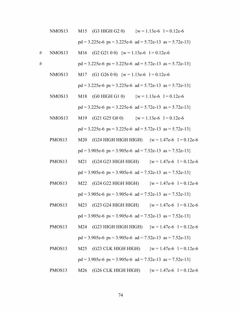
74
NMOS13 M15 (G3 HIGH G2 0) {w = 1.13e-6 l = 0.12e-6
pd = 3.225e-6 ps = 3.225e-6 ad = 5.72e-13 as = 5.72e-13}
# NMOS13 M16 (G2 G21 0 0) {w = 1.13e-6 l = 0.12e-6
# pd = 3.225e-6 ps = 3.225e-6 ad = 5.72e-13 as = 5.72e-13}
NMOS13 M17 (G1 G26 0 0) {w = 1.13e-6 l = 0.12e-6
pd = 3.225e-6 ps = 3.225e-6 ad = 5.72e-13 as = 5.72e-13}
NMOS13 M18 (G0 HIGH G1 0) {w = 1.13e-6 l = 0.12e-6
pd = 3.225e-6 ps = 3.225e-6 ad = 5.72e-13 as = 5.72e-13}
NMOS13 M19 (G21 G25 G0 0) {w = 1.13e-6 l = 0.12e-6
pd = 3.225e-6 ps = 3.225e-6 ad = 5.72e-13 as = 5.72e-13}
PMOS13 M20 (G24 HIGH HIGH HIGH) {w = 1.47e-6 l = 0.12e-6
pd = 3.905e-6 ps = 3.905e-6 ad = 7.52e-13 as = 7.52e-13}
PMOS13 M21 (G24 G23 HIGH HIGH) {w = 1.47e-6 l = 0.12e-6
pd = 3.905e-6 ps = 3.905e-6 ad = 7.52e-13 as = 7.52e-13}
PMOS13 M22 (G24 G22 HIGH HIGH) {w = 1.47e-6 l = 0.12e-6
pd = 3.905e-6 ps = 3.905e-6 ad = 7.52e-13 as = 7.52e-13}
PMOS13 M23 (G23 G24 HIGH HIGH) {w = 1.47e-6 l = 0.12e-6
pd = 3.905e-6 ps = 3.905e-6 ad = 7.52e-13 as = 7.52e-13}
PMOS13 M24 (G23 HIGH HIGH HIGH) {w = 1.47e-6 l = 0.12e-6
pd = 3.905e-6 ps = 3.905e-6 ad = 7.52e-13 as = 7.52e-13}
PMOS13 M25 (G23 CLK HIGH HIGH) {w = 1.47e-6 l = 0.12e-6
pd = 3.905e-6 ps = 3.905e-6 ad = 7.52e-13 as = 7.52e-13}
PMOS13 M26 (G26 CLK HIGH HIGH) {w = 1.47e-6 l = 0.12e-6

75
pd = 3.905e-6 ps = 3.905e-6 ad = 7.52e-13 as = 7.52e-13}
PMOS13 M27 (G26 G23 HIGH HIGH) {w = 1.47e-6 l = 0.12e-6
pd = 3.905e-6 ps = 3.905e-6 ad = 7.52e-13 as = 7.52e-13}
PMOS13 M28 (G26 G22 HIGH HIGH) {w = 1.47e-6 l = 0.12e-6
pd = 3.905e-6 ps = 3.905e-6 ad = 7.52e-13 as = 7.52e-13}
PMOS13 M29 (G22 D HIGH HIGH) {w = 1.47e-6 l = 0.12e-6
pd = 3.905e-6 ps = 3.905e-6 ad = 7.52e-13 as = 7.52e-13}
PMOS13 M30 (G22 HIGH HIGH HIGH) {w = 1.47e-6 l = 0.12e-6
pd = 3.905e-6 ps = 3.905e-6 ad = 7.52e-13 as = 7.52e-13}
PMOS13 M31 (G22 G26 HIGH HIGH) {w = 1.47e-6 l = 0.12e-6
pd = 3.905e-6 ps = 3.905e-6 ad = 7.52e-13 as = 7.52e-13}
PMOS13 M32 (G25 G23 HIGH HIGH) {w = 1.47e-6 l = 0.12e-6
pd = 3.905e-6 ps = 3.905e-6 ad = 7.52e-13 as = 7.52e-13}
PMOS13 M33 (G25 HIGH HIGH HIGH) {w = 1.47e-6 l = 0.12e-6
pd = 3.905e-6 ps = 3.905e-6 ad = 7.52e-13 as = 7.52e-13}
PMOS13 M34 (G25 G21 HIGH HIGH) {w = 1.47e-6 l = 0.12e-6
pd = 3.905e-6 ps = 3.905e-6 ad = 7.52e-13 as = 7.52e-13}
PMOS13 M35 (G21 G26 HIGH HIGH) {w = 1.47e-6 l = 0.12e-6
pd = 3.905e-6 ps = 3.905e-6 ad = 7.52e-13 as = 7.52e-13}
PMOS13 M36 (G21 HIGH HIGH HIGH) {w = 1.47e-6 l = 0.12e-6
pd = 3.905e-6 ps = 3.905e-6 ad = 7.52e-13 as = 7.52e-13}
PMOS13 M37 (G21 G25 HIGH HIGH) {w = 1.47e-6 l = 0.12e-6
pd = 3.905e-6 ps = 3.905e-6 ad = 7.52e-13 as = 7.52e-13}

76
PMOS13 M38 (Q G21 HIGH HIGH) {w = 1.47e-6 l = 0.12e-6
pd = 3.905e-6 ps = 3.905e-6 ad = 7.52e-13 as = 7.52e-13}
PMOS13 M39 (QBAR G25 HIGH HIGH) {w = 1.47e-6 l = 0.12e-6
pd = 3.905e-6 ps = 3.905e-6 ad = 7.52e-13 as = 7.52e-13}
####this is initializes the node outright to 0 volts, look at the manual for more
information###
###this is for the spice .plt file###
Plot "dffF" (time() v(HIGH) v(D) v(CLK) v(Q) v(QBAR) v(G26) v(G25) v(G23)
v(G21) v(G2))
}
Solve{
Coupled (iterations=100) {Circuit}
Coupled (iterations=100) {Poisson}
Coupled (iterations=100) {Poisson Circuit}
Coupled (iterations=100) {Poisson Circuit Contact}
Coupled (iterations=100) {Poisson Hole Contact Circuit}
Coupled (iterations=100) {Poisson Electron Hole Contact Circuit}
NewCurrentFile="transientdffF"
Transient (
InitialTime=0 FinalTime=35.9e-9
InitialStep=1e-12 MaxStep=7.5e-11 Increment=1.2)
{
coupled {device1.poisson device1.electron device1.hole device1.contact

77
circuit}
}
Transient (
InitialTime=35.9e-9 FinalTime=36.5e-9
InitialStep=1e-12 MaxStep=2.5e-12 Increment=1.2 )
{
coupled{device1.poisson device1.electron device1.hole device1.contact circuit}
Plot ( FilePrefix="imF" Time=(36e-9;36.05e-9;36.1e-9;36.15e-9;36.2e-
9;36.3e-9;36.5e-9) NoOverwrite)
}
Transient (
InitialTime=36.5e-9 FinalTime=50e-9
InitialStep=1e-12 MaxStep=7.5e-11
Increment=1.2 )
{
coupled{device1.poisson device1.electron device1.hole device1.contact circuit}
Plot (FilePrefix="laterF" Time=(37e-9;38e-9;40e-9) NoOverwrite)
}
}

78
Dessis file for 3D mixed-mode DICE Latch simulation
# This file contains the setup for the mixed-mode single event DICE Latch simulations,
# including the netlist for the DICE latch
###################################################################
DEVICE NFET1{
File {
Grid = "NMOS_msh.grd"
Doping = "NMOS_msh.dat"
Param = "dessis.par"
}
Electrode {
{ Name="Drain1" Voltage=0 }
{ Name="Gate1" Voltage=0 }
{ Name="Source1" Voltage=0 }
{ Name="Drain2" Voltage=0 }
{ Name="Gate2" Voltage=0 }
{ Name="Source2" Voltage=0 }
{ Name="Pwell" Voltage=0 }
{ Name="Substrate" Voltage=0 }
79
}
Physics {
Recombination(SRH Auger) #TPA_gen
Mobility( Phumob HighFieldsat Enormal)
EffectiveIntrinsicDensity( OldSlotboom )
Fermi
HeavyIon(
time=7e-9
length=5
wt_hi=0.05
location=(-0.885,0.1,0)
direction=(1,0,1)
LET_f=0.3128
Gaussian
Picocoulomb )
}
Plot {
Potential Electricfield
eDensity hDensity
eCurrent/Vector hCurrent/Vector
TotalCurrent/Vector
SRH Auger Avalanche
eMobility hMobility

80
eQuasiFermi hQuasiFermi
eGradQuasiFermi hGradQuasiFermi
eEparallel hEparallel
eMobility hMobility
eVelocity hVelocity
DonorConcentration Acceptorconcentration
Doping SpaceCharge
ConductionBand ValenceBand
BandGap Affinity
xMoleFraction
eTemperature hTemperature
HeavyIonChargeDensity
}
}
Math {
WallClock
Extrapolate
Derivatives
RelErrControl
Iterations=15
notdamped=100
Newdiscretization
Method=ILS

81
RecBoxIntegr
number_of_threads=2
}
File {
Output = "dice2Alog"
SPICEPath = "." ###path where your spice models are ###
Plot = "dice2Aplot.dat"
Current = "dice2Acurrent.plt"
}
System {
Vsource_pset DATA (D 0) {pwl= (
0.0e+00 1.2
2e-9 1.2
2.2e-9 0
20e-9 0
)
}
Vsource_pset CLOCK (CLK 0) {pwl= (
0.0e+00 0
4e-9 0
4.2e-9 1.2
20e-9 1.2
)

82
}
Vsource_pset VDD (HIGH 0) {dc = 1.2} ###voltage source (HIGH 0) are
node names###
Vsource_pset PRESET (PRE 0) {dc = 1.2} ###voltage
source (HIGH 0) are node names###
Vsource_pset CLEAR (CLR 0) {dc = 1.2} ###voltage
source (HIGH 0) are node names###
######## mosfet (drain gate source bulk) ####################
###This is the TCAD device,I am referencing the device above, and connecting the
electrodes to spice nodes##
NFET1 device1 ("Drain2"=N1
"Gate2"=CLKB1
"Source2"=N241
"Drain1"=N2
"Gate1"=CLK
"Source1"=N257
"Substrate"=0
"Pwell"=0)
###These are spice transistors, NMOS13 & PMOS13 are the names from the spice model
file, M0-M39 is the name I give it here (drain gate source bulk) ###
NMOS13 MN1 (QBAR N137 0 0) {w = 1.42e-6 l = 0.12e-6
pd = 3.805e-6 ps = 3.805e-6 ad = 7.25e-13 as = 7.25e-13}
83
NMOS13 MN2 (Q N7 0 0) {w = 1.42e-6 l = 0.12e-6
pd = 3.805e-6 ps = 3.805e-6 ad = 7.25e-13 as = 7.25e-13}
NMOS13 MN3 (N7 N5 N153 0) {w = 0.80e-6 l = 0.12e-6
pd = 2.565e-6 ps = 2.565e-6 ad = 3.98e-13 as = 3.98e-13}
NMOS13 MN4 (N153 CLR 0 0) {w = 0.80e-6 l = 0.12e-6
pd = 2.565e-6 ps = 2.565e-6 ad = 3.98e-13 as = 3.98e-13}
NMOS13 MN5 (N137 N8 0 0) {w = 0.46e-6 l = 0.12e-6
pd = 1.885e-6 ps = 1.885e-6 ad = 2.19e-13 as = 3.98e-13}
NMOS13 MN6 (N8 N6 N173 0) {w = 0.80e-6 l = 0.12e-6
pd = 2.565e-6 ps = 2.565e-6 ad = 3.98e-13 as = 3.98e-13}
NMOS13 MN7 (N173 CLR 0 0) {w = 0.80e-6 l = 0.12e-6
pd = 2.565e-6 ps = 2.565e-6 ad = 3.98e-13 as = 3.98e-13}
NMOS13 MN8 (N5 CLK N161 0) {w = 0.80e-6 l = 0.12e-6
pd = 2.565e-6 ps = 2.565e-6 ad = 3.98e-13 as = 3.98e-13}
NMOS13 MN9 (N161 N2 0 0) {w = 0.80e-6 l = 0.12e-6
pd = 2.565e-6 ps = 2.565e-6 ad = 3.98e-13 as = 3.98e-13}
NMOS13 MN10 (N5 CLKB1 N181 0) {w = 1.13e-6 l = 0.12e-6
pd = 3.225e-6 ps = 3.225e-6 ad = 5.72e-13 as = 5.72e-13}
NMOS13 MN11 (N181 N8 N177 0) {w = 1.13e-6 l = 0.12e-6
pd = 3.225e-6 ps = 3.225e-6 ad = 5.72e-13 as = 5.72e-13}
NMOS13 MN12 (N177 PRE 0 0) {w = 1.13e-6 l = 0.12e-6
pd = 3.225e-6 ps = 3.225e-6 ad = 5.72e-13 as = 5.72e-13}
NMOS13 MN13 (N6 CLKB2 N145 0) {w = 1.13e-6 l = 0.12e-6

84
pd = 3.225e-6 ps = 3.225e-6 ad = 5.72e-13 as = 5.72e-13}
NMOS13 MN14 (N145 N7 N149 0) {w = 1.13e-6 l = 0.12e-6
pd = 3.225e-6 ps = 3.225e-6 ad = 5.72e-13 as = 5.72e-13}
NMOS13 MN15 (N149 PRE 0 0) {w = 1.13e-6 l = 0.12e-6
pd = 3.225e-6 ps = 3.225e-6 ad = 5.72e-13 as = 5.72e-13}
NMOS13 MN16 (N6 CLK N189 0) {w = 0.80e-6 l = 0.12e-6
pd = 2.565e-6 ps = 2.565e-6 ad = 3.98e-13 as = 3.98e-13}
NMOS13 MN17 (N189 N1 0 0) {w = 0.80e-6 l = 0.12e-6
pd = 2.565e-6 ps = 2.565e-6 ad = 3.98e-13 as = 3.98e-13}
# NMOS13 MN18 (N2 CLK N257 0) {w = 1.13e-6 l = 0.12e-6
# pd = 3.225e-6 ps = 3.225e-6 ad = 5.72e-13 as = 5.72e-13}
NMOS13 MN19 (N257 N3 N253 0) {w = 1.13e-6 l = 0.12e-6
pd = 3.225e-6 ps = 3.225e-6 ad = 5.72e-13 as = 5.72e-13}
NMOS13 MN20 (N253 CLR 0 0) {w = 1.13e-6 l = 0.12e-6
pd = 3.225e-6 ps = 3.225e-6 ad = 5.72e-13 as = 5.72e-13}
NMOS13 MN21 (N2 CLKB2 N209 0) {w = 0.80e-6 l = 0.12e-6
pd = 2.565e-6 ps = 2.565e-6 ad = 3.98e-13 as = 3.98e-13}
NMOS13 MN22 (N209 D 0 0) {w = 0.80e-6 l = 0.12e-6
pd = 2.565e-6 ps = 2.565e-6 ad = 3.98e-13 as = 3.98e-13}
NMOS13 MN23 (CLKB1 CLK 0 0) {w = 0.46e-6 l = 0.12e-6
pd = 1.885e-6 ps = 1.885e-6 ad = 2.19e-13 as = 3.98e-13}
NMOS13 MN24 (CLKB2 CLK 0 0) {w = 0.46e-6 l = 0.12e-6
pd = 1.885e-6 ps = 1.885e-6 ad = 2.19e-13 as = 3.98e-13}

85
NMOS13 MN25 (N1 CLK N217 0) {w = 1.13e-6 l = 0.12e-6
pd = 3.225e-6 ps = 3.225e-6 ad = 5.72e-13 as = 5.72e-13}
NMOS13 MN26 (N217 N4 N221 0) {w = 1.13e-6 l = 0.12e-6
pd = 3.225e-6 ps = 3.225e-6 ad = 5.72e-13 as = 5.72e-13}
NMOS13 MN27 (N221 CLR 0 0) {w = 1.13e-6 l = 0.12e-6
pd = 3.225e-6 ps = 3.225e-6 ad = 5.72e-13 as = 5.72e-13}
# NMOS13 MN28 (N1 CLKB1 N241 0) {w = 0.80e-6 l = 0.12e-6
# pd = 2.565e-6 ps = 2.565e-6 ad = 3.98e-13 as = 3.98e-13}
NMOS13 MN29 (N241 D 0 0) {w = 0.80e-6 l = 0.12e-6
pd = 2.565e-6 ps = 2.565e-6 ad = 3.98e-13 as = 3.98e-13}
NMOS13 MN30 (N4 N2 N225 0) {w = 0.80e-6 l = 0.12e-6
pd = 2.565e-6 ps = 2.565e-6 ad = 3.98e-13 as = 3.98e-13}
NMOS13 MN31 (N225 PRE 0 0) {w = 0.80e-6 l = 0.12e-6
pd = 2.565e-6 ps = 2.565e-6 ad = 3.98e-13 as = 3.98e-13}
NMOS13 MN32 (N3 N1 N249 0) {w = 0.80e-6 l = 0.12e-6
pd = 2.565e-6 ps = 2.565e-6 ad = 3.98e-13 as = 3.98e-13}
NMOS13 MN33 (N249 PRE 0 0) {w = 0.80e-6 l = 0.12e-6
pd = 2.565e-6 ps = 2.565e-6 ad = 3.98e-13 as = 3.98e-13}
PMOS13 MP1 (QBAR N137 HIGH HIGH) {w = 4.3e-6 l = 0.12e-6
pd = 9.565e-6 ps = 9.565e-6 ad = 2.245e-12 as = 2.245e-12}
PMOS13 MP2 (Q N7 HIGH HIGH) {w = 4.3e-6 l = 0.12e-6
pd = 9.565e-6 ps = 9.565e-6 ad = 2.245e-12 as = 2.245e-12}
PMOS13 MP3 (N7 N6 HIGH HIGH) {w = 1.47e-6 l = 0.12e-6

86
pd = 3.905e-6 ps = 3.905e-6 ad = 7.52e-13 as = 7.52e-13}
PMOS13 MP4 (N7 CLR HIGH HIGH) {w = 1.47e-6 l = 0.12e-6
pd = 3.905e-6 ps = 3.905e-6 ad = 7.52e-13 as = 7.52e-13}
PMOS13 MP5 (N137 N8 HIGH HIGH){w = 1.47e-6 l = 0.12e-6
pd = 3.905e-6 ps = 3.905e-6 ad = 7.52e-13 as = 7.52e-13}
PMOS13 MP6 (N8 CLR HIGH HIGH) {w = 1.47e-6 l = 0.12e-6
pd = 3.905e-6 ps = 3.905e-6 ad = 7.52e-13 as = 7.52e-13}
PMOS13 MP7 (N8 N5 HIGH HIGH) {w = 1.47e-6 l = 0.12e-6
pd = 3.905e-6 ps = 3.905e-6 ad = 7.52e-13 as = 7.52e-13}
PMOS13 MP8 (N5 CLKB1 N32 HIGH) {w = 2.85e-6 l = 0.12e-6
pd = 6.665e-6 ps = 6.665e-6 ad = 1.48e-12 as = 1.48e-12}
PMOS13 MP9 (N32 N2 HIGH HIGH) {w = 2.85e-6 l = 0.12e-6
pd = 6.665e-6 ps = 6.665e-6 ad = 1.48e-12 as = 1.48e-12}
PMOS13 MP10 (N5 CLK N0471 HIGH) {w = 2.85e-6 l = 0.12e-6
pd = 6.665e-6 ps = 6.665e-6 ad = 1.48e-12 as = 1.48e-12}
PMOS13 MP11 (N0471 N7 HIGH HIGH){w = 2.85e-6 l = 0.12e-6
pd = 6.665e-6 ps = 6.665e-6 ad = 1.48e-12 as = 1.48e-12}
PMOS13 MP12 (N5 PRE HIGH HIGH){w = 1.47e-6 l = 0.12e-6
pd = 3.905e-6 ps = 3.905e-6 ad = 7.52e-13 as = 7.52e-13}
PMOS13 MP13 (N6 CLKB2 N64 HIGH) {w = 2.85e-6 l = 0.12e-6
pd = 6.665e-6 ps = 6.665e-6 ad = 1.48e-12 as = 1.48e-12}
PMOS13 MP14 (N64 N1 HIGH HIGH) {w = 2.85e-6 l = 0.12e-6
pd = 6.665e-6 ps = 6.665e-6 ad = 1.48e-12 as = 1.48e-12}

87
PMOS13 MP15 (N6 CLK N0435 HIGH) {w = 2.85e-6 l = 0.12e-6
pd = 6.665e-6 ps = 6.665e-6 ad = 1.48e-12 as = 1.48e-12}
PMOS13 MP16 (N0435 N8 HIGH HIGH) {w = 2.85e-6 l = 0.12e-6
pd = 6.665e-6 ps = 6.665e-6 ad = 1.48e-12 as = 1.48e-12}
PMOS13 MP17 (N6 PRE HIGH HIGH) {w = 1.47e-6 l = 0.12e-6
pd = 3.905e-6 ps = 3.905e-6 ad = 7.52e-13 as = 7.52e-13}
PMOS13 MP18 (N2 CLK N76 HIGH) {w = 2.85e-6 l = 0.12e-6
pd = 6.665e-6 ps = 6.665e-6 ad = 1.48e-12 as = 1.48e-12}
PMOS13 MP19 (N76 D HIGH HIGH) {w = 2.85e-6 l = 0.12e-6
pd = 6.665e-6 ps = 6.665e-6 ad = 1.48e-12 as = 1.48e-12}
PMOS13 MP20 (N2 CLR HIGH HIGH) {w = 1.47e-6 l = 0.12e-6
pd = 3.905e-6 ps = 3.905e-6 ad = 7.52e-13 as = 7.52e-13}
PMOS13 MP21 (N2 CLKB2 N0551 HIGH) {w = 2.85e-6 l = 0.12e-6
pd = 6.665e-6 ps = 6.665e-6 ad = 1.48e-12 as = 1.48e-12}
PMOS13 MP22 (N0551 N4 HIGH HIGH) {w = 2.85e-6 l = 0.12e-6
pd = 6.665e-6 ps = 6.665e-6 ad = 1.48e-12 as = 1.48e-12}
PMOS13 MP23 (CLKB1 CLK HIGH HIGH) {w = 1.47e-6 l = 0.12e-6
pd = 3.905e-6 ps = 3.905e-6 ad = 7.52e-13 as = 7.52e-13}
PMOS13 MP24 (CLKB2 CLK HIGH HIGH) {w = 1.47e-6 l = 0.12e-6
pd = 3.905e-6 ps = 3.905e-6 ad = 7.52e-13 as = 7.52e-13}
PMOS13 MP25 (N1 CLR HIGH HIGH) {w = 1.47e-6 l = 0.12e-6
pd = 3.905e-6 ps = 3.905e-6 ad = 7.52e-13 as = 7.52e-13}
PMOS13 MP26 (N1 CLKB1 N0515 HIGH) {w = 2.85e-6 l = 0.12e-6

88
pd = 6.665e-6 ps = 6.665e-6 ad = 1.48e-12 as = 1.48e-12}
PMOS13 MP27 (N0515 N3 HIGH HIGH) {w = 2.85e-6 l = 0.12e-6
pd = 6.665e-6 ps = 6.665e-6 ad = 1.48e-12 as = 1.48e-12}
PMOS13 MP28 (N1 CLK N112 HIGH) {w = 2.85e-6 l = 0.12e-6
pd = 6.665e-6 ps = 6.665e-6 ad = 1.48e-12 as = 1.48e-12}
PMOS13 MP29 (N112 D HIGH HIGH) {w = 2.85e-6 l = 0.12e-6
pd = 6.665e-6 ps = 6.665e-6 ad = 1.48e-12 as = 1.48e-12}
PMOS13 MP30 (N4 N1 HIGH HIGH) {w = 1.47e-6 l = 0.12e-6
pd = 3.905e-6 ps = 3.905e-6 ad = 7.52e-13 as = 7.52e-13}
PMOS13 MP31 (N4 PRE HIGH HIGH) {w = 1.47e-6 l = 0.12e-6
pd = 3.905e-6 ps = 3.905e-6 ad = 7.52e-13 as = 7.52e-13}
PMOS13 MP32 (N3 N2 HIGH HIGH) {w = 1.47e-6 l = 0.12e-6
pd = 3.905e-6 ps = 3.905e-6 ad = 7.52e-13 as = 7.52e-13}
PMOS13 MP33 (N3 PRE HIGH HIGH) {w = 1.47e-6 l = 0.12e-6
pd = 3.905e-6 ps = 3.905e-6 ad = 7.52e-13 as = 7.52e-13}
####this is initializes the node outright to 0 volts, look at the manual for more
information###
###this is for the spice .plt file###
Plot "dice2A" (time() v(Q) v(QBAR) v(PRE) v(N2) v(CLK) v(N257) v(N3)
v(N253) v(CLR) v(N1) v(CLKB1) v(N241) v(D) v(N137) v(N6) v(N8) v(N5) v(N32)
v(N0471) v(N7) v(N64) v(N0435) v(N0551) v(N4) v(N0515) v(N161) v(N189) v(N209)
v(N217) v(N221) )
}

89
Solve{
Coupled (iterations=100) {Circuit}
Coupled (iterations=100) {Poisson}
Coupled (iterations=100) {Poisson Circuit}
Coupled (iterations=100) {Poisson Circuit Contact}
Coupled (iterations=100) {Poisson Hole Contact Circuit}
Coupled (iterations=100) {Poisson Electron Hole Contact Circuit}
NewCurrentFile="transientdice2A"
Transient (
InitialTime=0 FinalTime=1.99e-9
InitialStep=1e-12 MaxStep=7.5e-11 Increment=1.2)
{
coupled {device1.poisson device1.electron device1.hole device1.contact
circuit}
}
Transient (
InitialTime=1.99e-9 FinalTime=2.21e-9
InitialStep=1e-12 MaxStep=2.5e-12 Increment=1.2)
{
coupled {device1.poisson device1.electron device1.hole device1.contact
circuit}
}
Transient (

90
InitialTime=2.21e-9 FinalTime=3.99e-9
InitialStep=2.5e-12 MaxStep=7.5e-11 Increment=1.2)
{
coupled {device1.poisson device1.electron device1.hole device1.contact
circuit}
}
Transient (
InitialTime=3.99e-9 FinalTime=4.21e-9
InitialStep=1e-12 MaxStep=2.5e-12 Increment=1.2)
{
coupled {device1.poisson device1.electron device1.hole device1.contact
circuit}
}
Transient (
InitialTime=4.21e-9 FinalTime=6.99e-9
InitialStep=1e-12 MaxStep=7.5e-11 Increment=1.2)
{
coupled {device1.poisson device1.electron device1.hole device1.contact
circuit}
}
Transient (
InitialTime=6.99e-9 FinalTime=7.5e-9
InitialStep=1e-12 MaxStep=2.5e-12 Increment=1.2 )

91
{
coupled{device1.poisson device1.electron device1.hole device1.contact circuit}
Plot ( FilePrefix="imdice2A" Time=(7e-9;7.05e-9;7.1e-9;7.25e-9;7.5e-9)
NoOverwrite)
}
Transient (
InitialTime=7.5e-9 FinalTime=20e-9
InitialStep=2.5e-12 MaxStep=7.5e-11 Increment=1.2 )
{
coupled{device1.poisson device1.electron device1.hole device1.contact circuit}
Plot (FilePrefix="laterdice2A" Time=(7.8e-9;8.5e-9) NoOverwrite)
}
}
92
REFERENCES
[1] L. W. Massengill, “SEU modeling and prediction techniques,” in IEEE NSREC Short
Course, 1993, pp. III-1–III-93.
[2] P. E. Dodd and L. W. Massengill, “Basic mechanisms and modeling of single-event
upset in digital microelectronics,” IEEE Trans. Nucl. Sci., vol. 50, pp. 583–602, June
2003.
[3] J. S. Fu, C. L. Axness, and H. T. Weaver, “Memory SEU simulations using 2-D
transport calculations,” IEEE Electron. Device Lett., vol. 6, pp. 422–424, Aug. 1985.
[4] D. Binder, E.C. Smith, and A. B. Holman, “Satellite anomalies from galactic cosmic
rays,” IEEE Trans. Nucl. Sci., vol. 22, pp. 2675-2680, Dec. 1975.
[5] T. Calin, M. Nicolaidis, and R. Velazco, “Upset Hardened Memory Design for
Submicron CMOS Technology,” IEEE Trans. Nucl. Sci., vol. 43, Issue 6, pp. 2874-
2878, Dec 1996.
[6] M. E. Law et al, “Device Modeling of Single Event Effects,” presented at the 2006
Nuclear and Space Radiation Effects Conference, Ponte Vedra Beach, FL.
[7] M. R. Pinto, and R. W. Dutton, “An Efficient Numerical-Model of CMOS Latch-
Up,” IEEE Electron Device Letters, pp. 414-417, Nov 1983.
[8] S. Selberherr, A. Schutz, and H. W. Poltz, “Minimos – a Two-Dimensional Mos-
Transistor Analyzer,” IEEE Trans. On Electron Devices, vol. 27, 1ssue 8, pp. 1540-
1550, Aug 1980.
[9] J. G. Rollins and J. Choma, “Mixed-Mode Pisces-Spice Coupled-Circuit and Device
Solver,” IEEE Trans. On Computer-Aided Design of Integrated Circuit and Systems,
vol. 7, Issue 8, pp. 862-867, Aug 1988.
[10] P. E. Dodd and F. W. Sexton, “Critical charge concepts for CMOS SRAMs,”
IEEE Trans. Nucl. Sci., vol. 42, Issue 6, pp. 1764-1771, Dec 1995.
[11] http://www.itrs.net/Common/2004Update/2004Update.htm.
[12] Nvidia GeForceFX 5700 Ultra Graphics Processor Structural Analysis (SAR-
0408-002), CHIPWORKS Inc., Ottawa, Canada, 2005.
[13] ACCRE Computing Cluster, Nashville, TN.
[14] E. L. Peterson, “Interpretation of Heavy Ion Cross Section Measurements,” IEEE

93
Trans. Nucl. Sci., vol. 43, pp. 952–959, June 1996.
[15] A. D. Tipton et al, “Multiple-Bit Upset in 130 nm CMOS Technology,” presented
at the 2006 Nuclear and Space Radiation Effects Conference, Ponte Vedra Beach, FL.
[16] M. Takai, T. Kishimoto, Y. Ohno, H. Sayama, K. Sonoda, S. Satoh, T. Nishimura,
H. Miyoshi, A. Kinomura, Y. Horino, and K. Fujii, “Soft error susceptibility and
immune structures in dynamic random access memories (DRAM's) investigated by
nuclear microprobes,” IEEE Trans. Nucl. Sci., vol. 43, pp. 696-704, Feb. 1996.
[17] R. L. Woodruff and P. J. Rudeck, “Three-dimensional numerical simulation of
single event upset of an SRAM cell,” IEEE Trans. Nucl. Sci., vol. 40, pp. 1795–1803,
Dec. 1993.
[18] P. E. Dodd, F. W. Sexton, G. L. Hash, M. R. Shaneyfelt, B. L. Draper, A. J.
Farino, and R. S. Flores, “Impact of technology trends on SEU in CMOS SRAMs,”
IEEE Trans. Nucl. Sci., vol. 43, pp. 2797–2804, Dec.1996.
[19] B.D. Olson, D. R. Ball, K. M. Warren, L. W. Massengill, N. F. Haddad,S. E.
Doyle, D. McMorrow, “Simultaneous single event charge sharing and parasitic
bipolar conduction in a highly-scaled SRAM design,” IEEE Trans. Nucl. Sci., vol. 52,
no. 6, pp. 2132 - 2136, Dec. 2005.
[20] J. D. Black, A. L. Sternberg, M. L. Alles, A. F. Witulski, B. L. Bhuva, L. W.
Massengill, J. M. Benedetto, M. P. Baze, J. L. Wert, and M. G. Hubert, “Multiple-Bit
Upset in 130 nm CMOS Technology,” IEEE Trans. Nucl. Sci., vol. 52, no. 6, pp.
2536 - 2541, Dec. 2005.
[21] M. P. Baze et al, “Heavy Ion Test Results on 13 Shift Registers in a 130nm
Process,” presented at the 2006 Single Event Effects Symposium, Long Beach, CA.
[22] W. Peterson, “Error-correcting codes,” 2nd ed., Cambridge :The MIT Press, 1980.
560p.
[23] R. Velazco, T. Calin, M. Nicolaidis, S. C. Moss, S. D. LaLumondiere, V. T. Tran,
and R. Koga, “SEU-hardened storage cell validation using a pulsed laser,” IEEE
Trans. Nucl. Sci., vol. 43, no. 6, pp. 2843–2848, Dec. 1996.
[24] L. W. Massengill, “Scaling vs. SEE Mitigation,” presented at the 2006 Single
Event Effects Symposium, Long Beach, CA.
[25] Y. Song, K. N.Vu, J. S. Cable, A. A.Witteles,W. A.Kolasinski, R.Koga, J. H.
Elder, J. V. Osborn, R. C. Martin, and N. M. Ghoniem, “Experimental and analytical
investigation of single event multiple bit upsets in polysilicon load 64 k NMOS
SRAMs,” IEEE Trans. Nucl. Sci., vol. NS-35, no. 6, pp. 1673–1677, Dec. 1988.
94
[26] S. E. Diehl, A. Ochoa, P. V. Dressendorfer, R. Koga, and W. A. Koloasinski
“Error Analysis and Prevention of Cosmic Ion-Induced Soft Errors in Static CMOS
RAMS,” IEEE Trans. Nucl. Sci., vol. 29, Issue 6, pp. 2032-2039, Dec 1982.
[27] A. Balasubramanian, B. L. Bhuva, J. D. Black, and L. W. Massengill “RHBD
Techniques for Mitigating Effects of Single Event Hits Using Guard-Gates,” IEEE
Trans. Nucl. Sci., vol. 52, Issue 6, pp. 2531 – 2535, Dec. 2005.
[28] A. L. Sternberg, Institute for Space and Defense Electronics, Vanderbilt
University, Nashville, TN, private communication, 2005.
[29] Synopsys User Manual Release 10, Synosys, Mountain View, CA. USA.
[30] J. Benedetto, C. Salomonson-Begay, and P. McGuirk, "Single Event Upset
Hardening Limitations in Deep Sub-Micron Digital Designs due to Critical Node
Crowding," presented at the 2005 Hardened Electronics and Radiation Technology
Conference, Tampa, Florida.