ambient light sensor ic series digital 16bit serial … is an digital ambient light sensor ic for...
TRANSCRIPT

1/17 www.rohm.com 2009.04- Rev.B© 2009 ROHM Co., Ltd. All rights reserved.
Ambient Light Sensor IC Series
Digital 16bit Serial Output Type Ambient Light Sensor IC
BH1750FVI Descriptions
BH1750FVI is an digital Ambient Light Sensor IC for I2C bus interface. This IC is the most suitable to obtain the ambient light data for adjusting LCD and Keypad backlight power of Mobile phone. It is possible to detect wide range at High resolution. ( 1 - 65535 lx ).
Features
1) I2C bus Interface ( f / s Mode Support ) 2) Spectral responsibility is approximately human eye response 3) Illuminance to Digital Converter 4) Wide range and High resolution. ( 1 - 65535 lx ) 5) Low Current by power down function 6) 50Hz / 60Hz Light noise reject-function 7) 1.8V Logic input interface 8) No need any external parts 9) Light source dependency is little. ( ex. Incandescent Lamp. Fluorescent Lamp. Halogen Lamp. White LED. Sun Light ) 10) It is possible to select 2 type of I2C slave-address. 11) Adjustable measurement result for influence of optical window ( It is possible to detect min. 0.11 lx, max. 100000 lx by using this function. ) 12) Small measurement variation (+/- 20%) 13) The influence of infrared is very small.
Applications
Mobile phone, LCD TV, NOTE PC, Portable game machine, Digital camera, Digital video camera, Car navigation, PDA, LCD display
Absolute Maximum Ratings
Parameter Symbol Limits Units
Supply Voltage Vmax 4.5 V
Operating Temperature Topr -40~85
Storage Temperature Tstg -40~100
SDA Sink Current Imax 7 mA
Power Dissipation Pd 260※ mW ※ 70mm × 70mm × 1.6mm glass epoxy board. Derating in done at 3.47mW/ for operating above Ta=25.
Operating Conditions
Parameter Symbol Min. Typ. Max. Units
VCC Voltage Vcc 2.4 3.0 3.6 V
I2C Reference Voltage VDVI 1.65 - VCC V
No.09046EBT01

BH1750FVI Technical Note
2/17 www.rohm.com 2009.04- Rev.B© 2009 ROHM Co., Ltd. All rights reserved.
Electrical Characteristics ( VCC = 3.0V, DVI = 3.0V, Ta = 25, unless otherwise noted )
Parameter Symbol Min. Typ. Max. Units Conditions
Supply Current Icc1 - 120 190 µA Ev = 100 lx ※1
Powerdown Current Icc2 - 0.01 1.0 µA No input Light
Peak Wave Length λp - 560 - nm
Measurement Accuracy S/A 0.96 1.2 1.44 times Sensor out / Actual lx EV = 1000 lx ※1, ※2
Dark ( 0 lx ) Sensor out S0 0 0 3 count H-Resolution Mode ※3
H-Resolution Mode Resolution rHR - 1 - lx
L-Resolution Mode Resolution rLR - 4 - lx
H-Resolution Mode Measurement Time tHR - 120 180 ms
L-Resolution Mode Measurement Time tLR - 16 24 ms
Incandescent / Fluorescent Sensor out ratio
rIF - 1 - times EV = 1000 lx
ADDR Input ‘H’ Voltage VAH 0.7 * VCC - - V
ADDR Input ‘L’ Voltage VAL - - 0.3 * VCC V
DVI Input ‘L’ Voltage VDVL - - 0.4 V
SCL, SDA Input ‘H’ Voltage 1 VIH1 0.7 * DVI - - V DVI ≧ 1.8V
SCL, SDA Input ‘H’ Voltage 2 VIH2 1.26 - - V 1.65V ≦ DVI <1.8V
SCL, SDA Input ‘L’ Voltage 1 VIL1 - - 0.3 * DVI V DVI ≧ 1.8V
SCL, SDA Input ‘L’ Voltage 2 VIL2 - - DVI – 1.26 V 1.65V ≦ DVI < 1.8V
SCL, SDA, ADDR Input ‘H’ Current IIH - - 10 µA
SCL, SDA, ADDR Input ‘L’ Current IIL - - 10 µA
I2C SCL Clock Frequency fSCL - - 400 kHz
I2C Bus Free Time tBUF 1.3 - - µs
I2C Hold Time ( repeated ) START Condition
tHDSTA 0.6 - - µs
I2C Set up time for a Repeated START Condition
tSUSTA 0.6 - - µs
I2C Set up time for a Repeated STOP Condition tSUSTD 0.6 - - µs
I2C Data Hold Time tHDDAT 0 - 0.9 µs
I2C Data Setup Time tSUDAT 100 - - ns
I2C ‘L’ Period of the SCL Clock tLOW 1.3 - - µs
I2C ‘H’ Period of the SCL Clock tHIGH 0.6 - - µs
I2C SDA Output ‘L’ Voltage VOL 0 - 0.4 V IOL = 3 mA
※1 White LED is used as optical source. ※2 Measurement Accuracy typical value is possible to change '1' by "Measurement result adjustment function". ※3 Use H-resolution mode or H-resolution mode2 if dark data ( less than 10 lx ) is need.

BH1750FVI Technical Note
3/17 www.rohm.com 2009.04- Rev.B© 2009 ROHM Co., Ltd. All rights reserved.
Reference Data
0
0.2
0.4
0.6
0.8
1
1.2
-90 -60 -30 0 30 60 90Angle [ deg ]
Rat
io
0
0.2
0.4
0.6
0.8
1
1.2
-90 -60 -30 0 30 60 90
Angle [ deg ]
Ra
tio
Fig.8 Light Source Dependency ( Fluorescent Light is set to '1' )
1
10
100
1000
10000
100000
1 10 100 1000 10000 100000
Illuminance [ lx ]
Me
asu
rem
en
t R
esu
lt
Fig.4 Directional Characteristics 1 Fig.5 Directional Characteristics 2
Fig.6 Dark Response
蛍光灯白熱灯感度比
0
2
4
6
8
10
-40 -20 0 20 40 60 80 100
Ta [ ]
Me
asu
rem
en
t R
esu
lt
0
50
100
150
200
2 2.5 3 3.5 4
VCC [ V ]
ICC
@ M
ea
sure
me
nt
H-Res. L-Res.
0
8
16
24
32
40
48
56
64
0 8 16 24 32 40 48 56 64
Illuminance [ lx ]
Me
asu
rem
en
t R
esu
lt
H-Res.
L-Res.
H-Res.
-
+
-
+
-
+
-
+
1pin
1pin
Fig.7 Measurement Accuracy Temperature Dependency
Fig.2 Illuminance - Measurement Result 1
Fig.3 Illuminance - Measuremnet Result 2
Fig.9 VCC - ICC ( During measurement )
Fig.10 VCC – ICC@0 Lx ( POWER DOWN )
Fig.1 Spectral Response
0
0.2
0.4
0.6
0.8
1
1.2
2 2.5 3 3.5 4VCC [ V ]
Ra
tio
Fig.11 Measurement Result VCC Dependency
0
0.2
0.4
0.6
0.8
1
1.2
1.5 2 2.5 3 3.5
DVI [ V ]
Ra
tio
Fig.12 Measurement Result DVI Dependency
DVI=1.8V VCC=3V
0
0.2
0.4
0.6
0.8
1
1.2
400 500 600 700 800 900 1000 1100
Wavelength [ nm ]
Rat
io
0 0.5 1 1.5 2
FluorescentLight
IncandescentLight
HalogenLight
Kripton Light
Artifical SunLight
White LED
Ratio
0
0.2
0.4
0.6
0.8
1
1.2
-40 -20 0 20 40 60 80 100
Ta [ ]
Ra
tio
0.01
0.1
1
10
-40 -20 0 20 40 60 80 100
Ta [ ]
ICC
@ P
OW
ER
DO
WN
[ u
A ]

BH1750FVI Technical Note
4/17 www.rohm.com 2009.04- Rev.B© 2009 ROHM Co., Ltd. All rights reserved.
Block Diagram
Block Diagram Descriptions
・PD
Photo diode with approximately human eye response. ・AMP
Integration-OPAMP for converting from PD current to Voltage. ・ADC
AD converter for obtainment Digital 16bit data. ・Logic + I2C Interface
Ambient Light Calculation and I2C BUS Interface. It is including below register.
Data Register → This is for registration of Ambient Light Data. Initial Value is "0000_0000_0000_0000".
Measurement Time Register → This is for registration of measurement time. Initial Value is "0100_0101". ・OSC
Internal Oscillator ( typ. 320kHz ). It is CLK for internal logic.
Measurement Procedure
* "Power On" Command is possible to omit.
SCL SDA
GND ADDR
PD
VCC DVI
Logic+
I2C Interface
ADC AMP
OSC
State Transition by I2C write-command.
Automatically State Transition
State is automatically changed to
Power Down mode.
Power supply
Power Down
Power On
Measurement Command
Initial state is Power Down mode after
VCC and DVI supply.
One Time Measurement Continuous Measurement

BH1750FVI Technical Note
5/17 www.rohm.com 2009.04- Rev.B© 2009 ROHM Co., Ltd. All rights reserved.
Instruction Set Architecture
Instruction Opecode Comments
Power Down 0000_0000 No active state.
Power On 0000_0001 Waiting for measurement command.
Reset 0000_0111 Reset Data register value. Reset command is not acceptable in Power Down mode.
Continuously H-Resolution Mode 0001_0000 Start measurement at 1lx resolution. Measurement Time is typically 120ms.
Continuously H-Resolution Mode2 0001_0001 Start measurement at 0.5lx resolution. Measurement Time is typically 120ms.
Continuously L-Resolution Mode 0001_0011 Start measurement at 4lx resolution. Measurement Time is typically 16ms.
One Time H-Resolution Mode 0010_0000 Start measurement at 1lx resolution. Measurement Time is typically 120ms. It is automatically set to Power Down mode after measurement.
One Time H-Resolution Mode2 0010_0001 Start measurement at 0.5lx resolution. Measurement Time is typically 120ms. It is automatically set to Power Down mode after measurement.
One Time L-Resolution Mode 0010_0011 Start measurement at 4lx resolution. Measurement Time is typically 16ms. It is automatically set to Power Down mode after measurement.
Change Measurement time ( High bit )
01000_MT[7,6,5]Change measurement time. ※ Please refer "adjust measurement result for influence of optical window."
Change Masurement time ( Low bit )
011_MT[4,3,2,1,0]Change measurement time. ※ Please refer "adjust measurement result for influence of optical window."
※ Don't input the other opecode.
Measurement mode explanation
Measurement Mode Measurement Time. Resolurtion
H-resolution Mode2 Typ. 120ms. 0.5 lx
H-Resolution Mode Typ. 120ms. 1 lx.
L-Resolution Mode Typ. 16ms. 4 lx.
We recommend to use H-Resolution Mode.
Measurement time ( integration time ) of H-Resolution Mode is so long that some kind of noise( including in 50Hz / 60Hz noise ) is rejected. And H-Resolution Mode is 1 l x resolution so that it is suitable for darkness ( less than 10 lx ) H-resolution mode2 is also suitable to detect for darkness.
Explanation of Asynchronous reset and Reset command "0000_0111"
1) Asynchronous reset All registers are reset. It is necessary on power supply sequence. Please refer "Timing chart for VCC and DVI power supply sequence" in this page. It is power down mode during DVI = 'L'.
2) Reset command Reset command is for only reset Illuminance data register. ( reset value is '0' ) It is not necessary even power supply sequence.It is used for removing previous measurement result. This command is not working in power down mode, so that please set the power on mode before input this command.
BH1750FVI Technical Note
6/17 www.rohm.com 2009.04- Rev.B© 2009 ROHM Co., Ltd. All rights reserved.
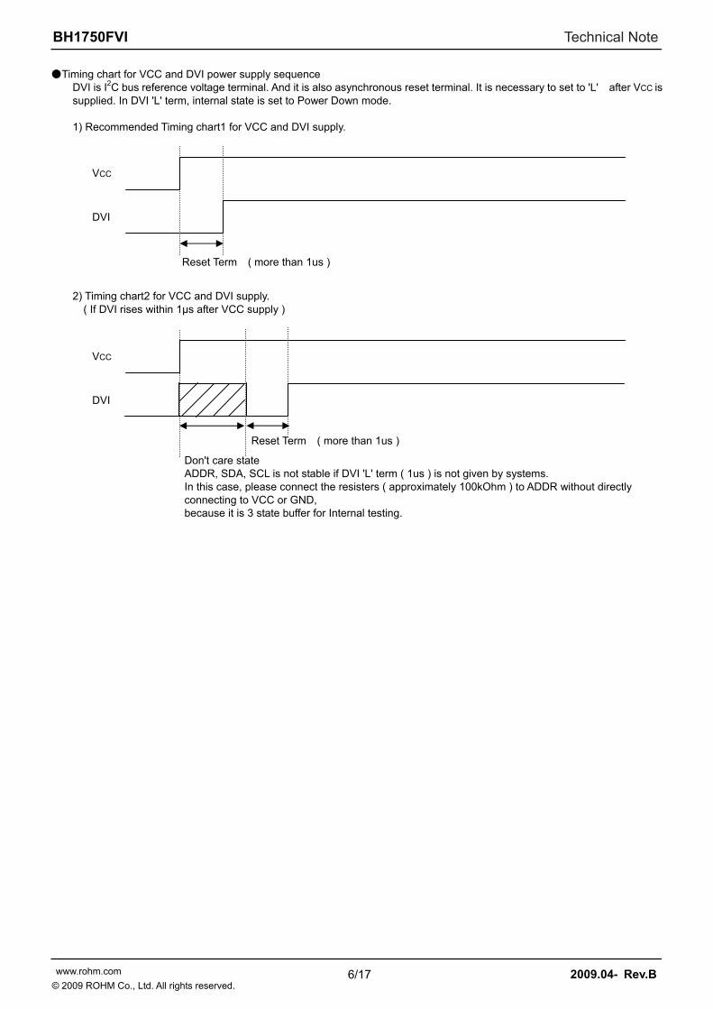
Timing chart for VCC and DVI power supply sequence DVI is I2C bus reference voltage terminal. And it is also asynchronous reset terminal. It is necessary to set to 'L' after VCC is supplied. In DVI 'L' term, internal state is set to Power Down mode. 1) Recommended Timing chart1 for VCC and DVI supply.
2) Timing chart2 for VCC and DVI supply.
( If DVI rises within 1µs after VCC supply )
VCC
DVI
Reset Term ( more than 1us )
VCC
DVI
Don't care state ADDR, SDA, SCL is not stable if DVI 'L' term ( 1us ) is not given by systems. In this case, please connect the resisters ( approximately 100kOhm ) to ADDR without directly connecting to VCC or GND, because it is 3 state buffer for Internal testing.
Reset Term ( more than 1us )

BH1750FVI Technical Note
7/17 www.rohm.com 2009.04- Rev.B© 2009 ROHM Co., Ltd. All rights reserved.
Measurement sequence example from "Write instruction" to "Read measurement result" ex1) Continuously H-resolution mode ( ADDR = 'L' )
① Send "Continuously H-resolution mode " instruction
ST 0100011 0 Ack 00010000 Ack SP
② Wait to complete 1st H-resolution mode measurement.( max. 180ms. )
③ Read measurement result.
ST 0100011 1 Ack High Byte [ 15:8 ] Ack
Low Byte [ 7:0 ] Ack SP
How to calculate when the data High Byte is "10000011" and Low Byte is "10010000" ( 215 + 29 + 28 + 27 + 24 ) / 1.2 ≒ 28067 [ lx ] The result of continuously measurement mode is updated.( 120ms.typ at H-resolution mode, 16ms.typ at L-resolution mode )
ex2 ) One time L-resolution mode ( ADDR = 'H' )
① Send "One time L-resolution mode " instruction
ST 1011100 0 Ack 00100011 Ack SP
② Wait to complete L-resolution mode measurement.( max. 24ms. )
③ Read measurement result
ST 1011100 1 Ack High Byte [ 15:8 ] Ack
Low Byte [ 7:0 ] Ack SP
How to calculate when the data High Byte is "00000001" and Low Byte is "00010000" ( 28 + 24 ) / 1.2 ≒ 227 [ lx ] In one time measurement, Statement moves to power down mode after measurement completion.If updated result is need then please resend measurement instruction.
from Master to Slave from Slave to Master
BH1750FVI Technical Note
8/17 www.rohm.com 2009.04- Rev.B© 2009 ROHM Co., Ltd. All rights reserved.
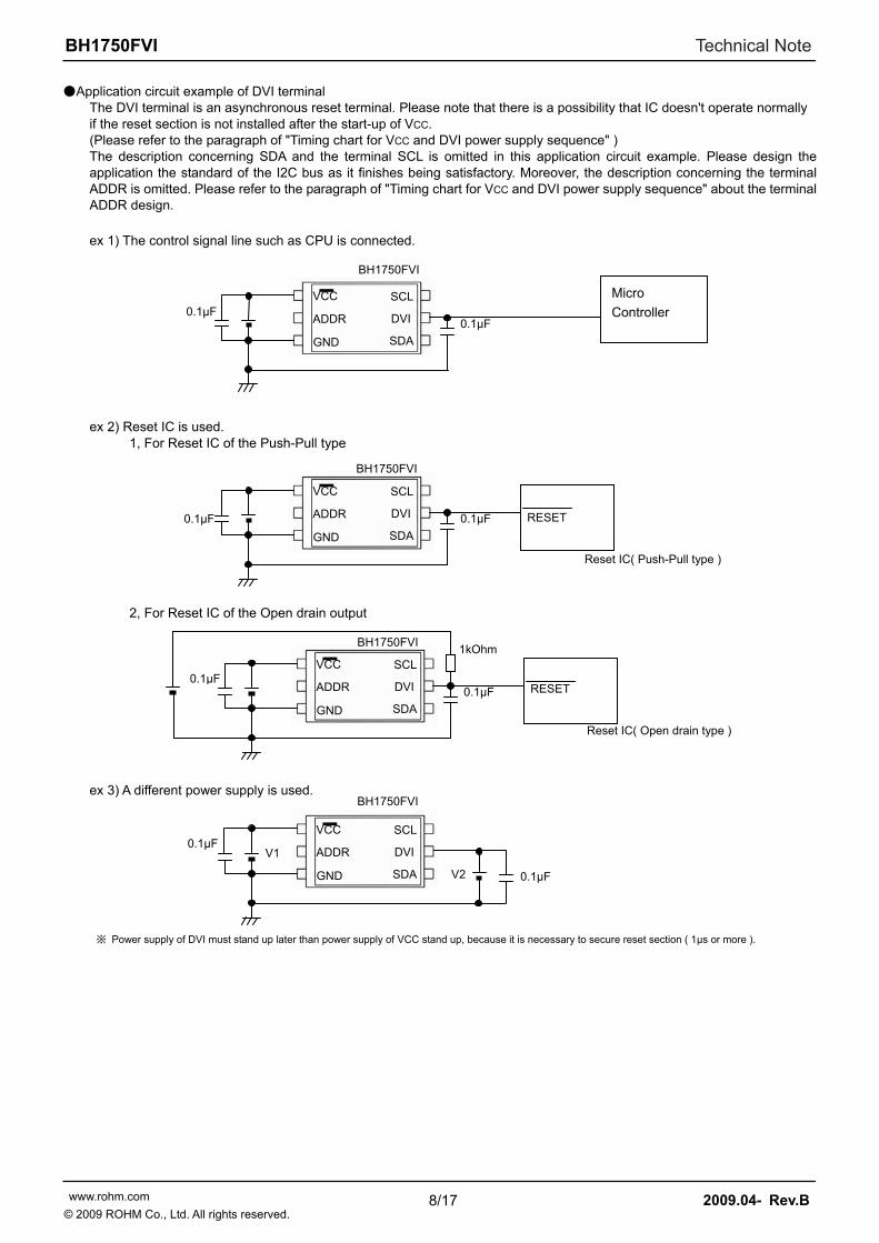
Application circuit example of DVI terminal The DVI terminal is an asynchronous reset terminal. Please note that there is a possibility that IC doesn't operate normally if the reset section is not installed after the start-up of VCC. (Please refer to the paragraph of "Timing chart for VCC and DVI power supply sequence" ) The description concerning SDA and the terminal SCL is omitted in this application circuit example. Please design the application the standard of the I2C bus as it finishes being satisfactory. Moreover, the description concerning the terminal ADDR is omitted. Please refer to the paragraph of "Timing chart for VCC and DVI power supply sequence" about the terminal ADDR design.
ex 1) The control signal line such as CPU is connected.
ex 2) Reset IC is used. 1, For Reset IC of the Push-Pull type
2, For Reset IC of the Open drain output
ex 3) A different power supply is used.
※ Power supply of DVI must stand up later than power supply of VCC stand up, because it is necessary to secure reset section ( 1µs or more ).
Micro
Controller VCC
ADDR
SCL
SDA
0.1µF 0.1µF DVI
GND
BH1750FVI
BH1750FVI
VCC
ADDR
SCL
SDA 0.1µF
DVI
GND
0.1µF
V2
V1
VCC
ADDR
SCL
SDA
0.1µF DVI
GND
RESET
Reset IC( Push-Pull type )
BH1750FVI
0.1µF
VCC
ADDR
SCL
SDA
0.1µF DVI
GND
Reset IC( Open drain type )
RESET
1kOhm BH1750FVI
0.1µF

BH1750FVI Technical Note
9/17 www.rohm.com 2009.04- Rev.B© 2009 ROHM Co., Ltd. All rights reserved.
ex 4) LPF using CR is inserted between VCC and DVI. This method has the possibility that the Reset section of turning on the power supply can not satisfied. cannot be satisfied. Please design the set considering the characteristic of the power supply enough.
Notes when CR is inserted between VCC and DVI
※ Please note that there is a possibility that reset section ( 1µs ) can not be satisfied because the power supply is turned on when the rise time of VCC is slow ※ When VCC is turned off, the DVI voltage becomes higher than VCC voltage but IC destruction is not occred if recommended constant ( R1 = 1kOhm, C1 = 1µF ) is used. ※ Please note that there is a possibility that Reset section (1µsec) cannot be satisfied if wait time is not enough long after turning off VCC. (It is necessary to consider DVI voltage level after turning off VCC.)
* Please do the application design to secure Reset section 1us or more after the reclosing of the power supply.
Example of designing set when CR ( C = 1µF, R = 1kΩ ) is inserted between VCC and DVI with VCC=2.8V
①The rise time to 0→2.4V of VCC must use the power supply of 100µs or less. ②Please wait 25ms or more after VCC turn off ( VCC <= 0.05V ), because it is necessary to secure reset section ( 1µs or more ).
R1 : 1kOhm
0.1µF C1 : 1µF
VCC
ADDR
GND
SCL
DVI
SDA
BH1750FVI
Reset Section : 1us or more
t1 VCC
DVI
2.4V
0.4V
0V
* Please do the application design to secure Reset section 1us or more after the reclosing of the power supply.
Reset Section : 1us or more
Rise time of power supply : 100us or less
0.05V
Time to power supply reclosing : 25ms or more
れVCC
DVI
2.4V
0.4V
2.8V
0V
t2

BH1750FVI Technical Note
10/17 www.rohm.com 2009.04- Rev.B© 2009 ROHM Co., Ltd. All rights reserved.
I2C Bus Access 1 ) I2C Bus Interface Timing chart
Write measurement command and Read measurement result are done by I2C Bus interface. Please refer the formally specification of I2C Bus interface, and follow the formally timing chart.
2) Slave Address
Slave Address is 2 types, it is determined by ADDR Terminal ADDR = ‘H’ ( ADDR ≧ 0.7VCC ) → “1011100“ ADDR = 'L' ( ADDR ≦ 0.3VCC ) → “0100011“
3 ) Write Format BH1750FVI is not able to accept plural command without stop condition. Please insert SP every 1 Opecode.
ST Slave Address R/W0 Ack Opecode Ack SP
4 ) Read Format
ST Slave Address R/W 1 Ack High Byte [15:8]
215 214 213 212 211 210 29 28 Ack
Low Byte [7:0] 27 26 25 24 23 22 21 20 Ack SP
ex )
High Byte = "1000_0011" Low Byte = "1001_0000"
( 215 + 29 + 28 + 27 + 24 ) / 1.2 ≒ 28067 [ lx ]
* I2C BUS is trademark of Phillips Semiconductors. Please refer formality specification.
from Master to Slave from Slave to Master
tHD ; DAT
S
SDA
SCL
S
tHD ; STA
tLOW tf tr
t Sr tSU ; STA
tSU ; DAT tf tHD
tSU;STO
tBUF
SP
tr
S tHIGH
tHD ; STA

BH1750FVI Technical Note
11/17 www.rohm.com 2009.04- Rev.B© 2009 ROHM Co., Ltd. All rights reserved.
Adjust measurement result for influence of optical window. ( sensor sensitivity adjusting ) BH1750FVI is possible to change sensor sensitivity. And it is possible to cancel the optical window influence ( difference with / without optical window ) by using this function. Adjust is done by changing measurement time. For example, when transmission rate of optical window is 50% ( measurement result becomes 0.5 times if optical window is set ), influence of optical window is ignored by changing sensor sensitivity from default to 2 times Sensor sensitivity is shift by changing the value of MTreg ( measurement time regisiter ). MTreg value has to set 2 times if target of sensor sensitivity is 2 times. Measurement time is also set 2 times when MTreg value is changed from default to 2 times. ex) Procedure for changing target sensor sensitivity to 2 times.
Please change Mtreg from ”0100_0101” ( default ) to ”1000_1010” ( default * 2 ).
1) Changing High bit of MTreg
ST Slave Address R/W
0 Ack 01000_100 Ack SP
2) Changing Low bit of MTreg
ST Slave Address R/W
0 Ack 011_01010 Ack SP
3) Input Measurement Command
ST Slave Address R/W
0 Ack 0001_0000 Ack SP
* This example is High Resolution mode, but it accepts the other measurement.
4) After about 240ms, measurement result is registered to Data Register. ( High Resolution mode is typically 120ms, but measurement time is set twice. )
The below table is seeing the changable range of MTreg.
Min. Typ. Max.
changable range of MTreg
binary 0001_1111
( sensitivity : default * 0.45 )0100_0101
default 1111_1110
( sensitivity : default * 3.68 )
decimal 31
( sensitivity : default * 0.45 )69
default 254
( sensitivity : default * 3.68 )
It is possilbe to detect 0.23lx by using this function at H-resolution mode. And it is possilbe to detect 0.11lx by using this function at H-resolution mode2. The below formula is to calculate illuminance per 1 count.
H-reslution mode : Illuminance per 1 count ( lx / count ) = 1 / 1.2 *( 69 / X ) H-reslution mode2 : Illuminance per 1 count ( lx / count ) = 1 / 1.2 *( 69 / X ) / 2
1.2 : Measurement accuracy 69 : Default value of MTreg ( dec ) X : MTreg value
The below table is seeing the detail of resolution.
Mtreg の値 lx / count
at H-resolutin mode lx / count
at H-resolution mode2
0001_1111 1.85 0.93
0100_0101 0.83 0.42
1111_1110 0.23 0.11
BH1750FVI Technical Note
12/17 www.rohm.com 2009.04- Rev.B© 2009 ROHM Co., Ltd. All rights reserved.
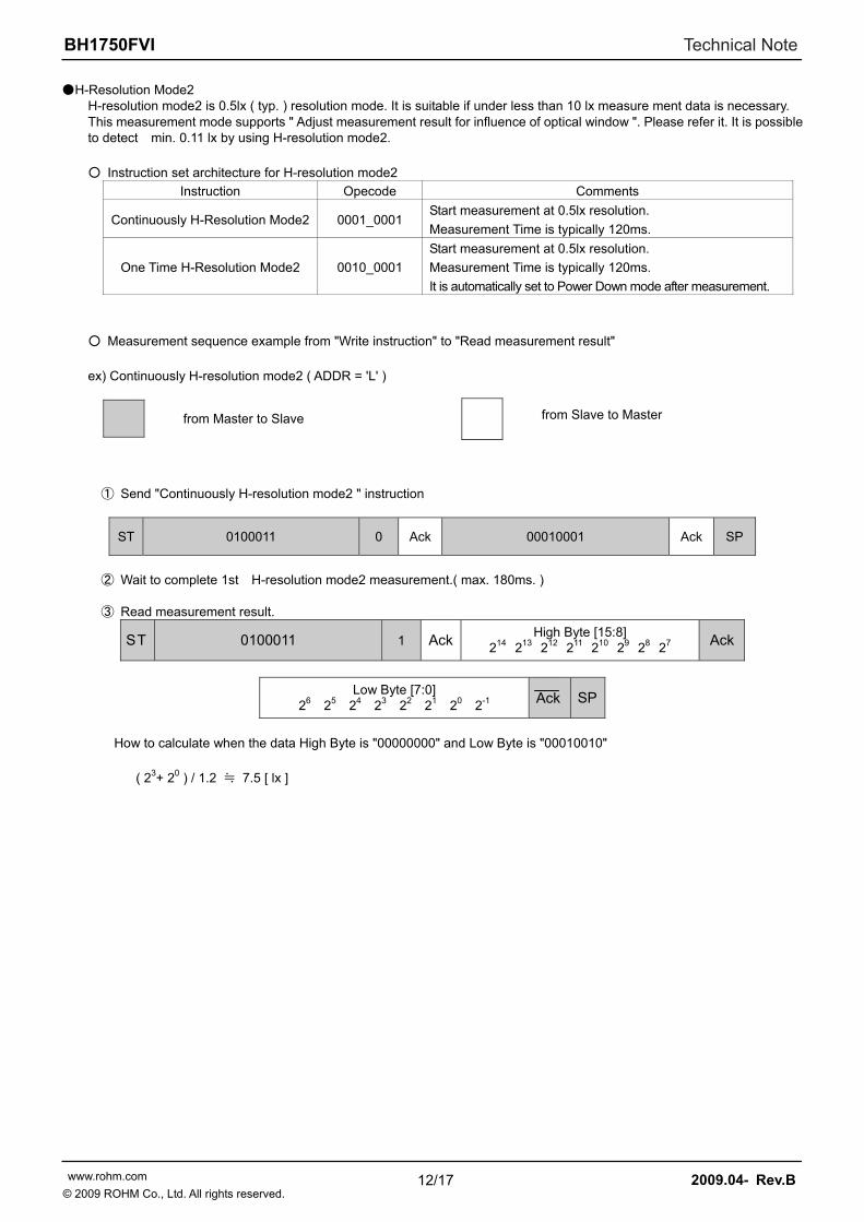
H-Resolution Mode2 H-resolution mode2 is 0.5lx ( typ. ) resolution mode. It is suitable if under less than 10 lx measure ment data is necessary. This measurement mode supports " Adjust measurement result for influence of optical window ". Please refer it. It is possible to detect min. 0.11 lx by using H-resolution mode2.
Instruction set architecture for H-resolution mode2
Instruction Opecode Comments
Continuously H-Resolution Mode2 0001_0001 Start measurement at 0.5lx resolution.
Measurement Time is typically 120ms.
One Time H-Resolution Mode2 0010_0001
Start measurement at 0.5lx resolution.
Measurement Time is typically 120ms.
It is automatically set to Power Down mode after measurement.
Measurement sequence example from "Write instruction" to "Read measurement result"
ex) Continuously H-resolution mode2 ( ADDR = 'L' )
① Send "Continuously H-resolution mode2 " instruction
ST 0100011 0 Ack 00010001 Ack SP
② Wait to complete 1st H-resolution mode2 measurement.( max. 180ms. ) ③ Read measurement result.
ST 0100011 1 AckHigh Byte [15:8]
214 213 212 211 210 29 28 27 Ack
Low Byte [7:0] 26 25 24 23 22 21 20 2-1 Ack SP
How to calculate when the data High Byte is "00000000" and Low Byte is "00010010" ( 23+ 20 ) / 1.2 ≒ 7.5 [ lx ]
from Master to Slave from Slave to Master

BH1750FVI Technical Note
13/17 www.rohm.com 2009.04- Rev.B© 2009 ROHM Co., Ltd. All rights reserved.
Terminal Description
PIN No. Terminal Name Equivalent Circuit Function
1 VCC Power Supply Terminal
2 ADDR
I2C Slave-address Terminal ADDR = ‘H’ ( ADDR ≧ 0.7VCC ) “1011100“ ADDR = 'L' ( ADDR ≦ 0.3VCC ) “0100011“ ADDR Terminal is designed as 3 state buffer for internal test. So that please take care of VCC and DVI supply procedure.Please see P6.
3 GND
GND Terminal
4 SDA
I2C bus Interface SDA Terminal
5 DVI
SDA, SCL Reference Voltage Terminal And DVI Terminal is also asynchronous Reset for internal registers.So that please set to 'L' ( at least 1µs, DVI <= 0.4V ) after VCC is supplied. BH1750FVI is pulled down by 150kOhm while DVI = 'L'.
6 SCL
I2C bus Interface SCL Terminal
※These values are design-value, not guaranteed.
150kΩ
VCC
BH1750FVI Technical Note
14/17 www.rohm.com 2009.04- Rev.B© 2009 ROHM Co., Ltd. All rights reserved.
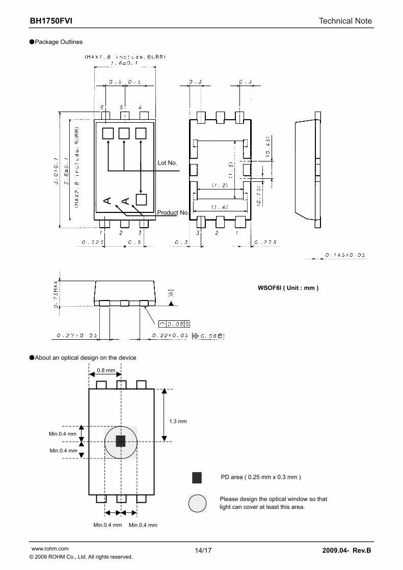
0.8 mm
1.3 mm
PD area ( 0.25 mm x 0.3 mm )
Please design the optical window so that light can cover at least this area.
Min.0.4 mm
Min.0.4 mm
Min.0.4 mm Min.0.4 mm
Package Outlines
About an optical design on the device
WSOF6I ( Unit : mm )
A
Lot No.
A
Product No.

BH1750FVI Technical Note
15/17 www.rohm.com 2009.04- Rev.B© 2009 ROHM Co., Ltd. All rights reserved.
The method of distinguishing 1pin.
There is some method of distinguishing 1pin. ① Distinguishing by 1Pin wide-lead ② Distinguishing by die pattern ③ Distinguishing by taper part of 1-3pin side
② (by die patern) is the easiest method to distinguish by naked eye.
A
A
Production code
①
②
③
BH1750FVI Technical Note
16/17 www.rohm.com 2009.04- Rev.B© 2009 ROHM Co., Ltd. All rights reserved.
Cautions on use
1) Absolute Maximum Ratings An excess in the absolute maximum ratings, such as supply voltage ( Vmax ), temperature range of operating conditions ( Topr ), etc., can break down devices, thus making impossible to identify breaking mode such as a short circuit or an open circuit. If any special mode exceeding the absolute maximum ratings is assumed, consideration should be given to take physical safety measures including the use of fuses, etc.
2) GND voltage Make setting of the potential of the GND terminal so that it will be maintained at the minimum in any operating state. Furthermore, check to be sure no terminals are at a potential lower than the GND voltage including an actual electric transient.
3) Short circuit between terminals and erroneous mounting In order to mount ICs on a set PCB, pay thorough attention to the direction and offset of the ICs. Erroneous mounting can break down the ICs. Furthermore, if a short circuit occurs due to foreign matters entering between terminals or between the terminal and the power supply or the GND terminal, the ICs can break down.
4) Operation in strong electromagnetic field Be noted that using ICs in the strong electromagnetic field can malfunction them.
5) Inspection with set PCB On the inspection with the set PCB, if a capacitor is connected to a low-impedance IC terminal, the IC can suffer stress. Therefore, be sure to discharge from the set PCB by each process. Furthermore, in order to mount or dismount the set PCB to/from the jig for the inspection process, be sure to turn OFF the power supply and then mount the set PCB to the jig. After the completion of the inspection, be sure to turn OFF the power supply and then dismount it from the jig. In addition, for protection against static electricity, establish a ground for the assembly process and pay thorough attention to the transportation and the storage of the set PCB.
6) Input terminals In terms of the construction of IC, parasitic elements are inevitably formed in relation to potential. The operation of the parasitic element can cause interference with circuit operation, thus resulting in a malfunction and then breakdown of the input terminal. Therefore, pay thorough attention not to handle the input terminals; such as to apply to the input terminals a voltage lower than the GND respectively, so that any parasitic element will operate. Furthermore, do not apply a voltage to the input terminals when no power supply voltage is applied to the IC. In addition, even if the power supply voltage is applied, apply to the input terminals a voltage lower than the power supply voltage or within the guaranteed value of electrical characteristics.
7) Thermal design Perform thermal design in which there are adequate margins by taking into account the power dissipation ( Pd ) in actual states of use.
8) Treatment of package Dusts or scratch on the photo detector may affect the optical characteristics. Please handle it with care.
9) Rush current When power is first supplied to the CMOS IC, it is possible that the internal logic may be unstable and rush current may flow instantaneously. Therefore, give special consideration to power coupling capacitance, power wiring, width of GND wiring, and routing of connections.
10) The exposed central pad on the back side of the package There is an exposed central pad on the back side of the package. But please do it non connection. ( Don't solder, and don't do electrical connection ) Please mount by Footprint dimensions described in the Jisso Information for WSOF6I. This pad is GND level, therefore there is a possibility that LSI malfunctions and heavy-current is generated.

BH1750FVI Technical Note
17/17 www.rohm.com 2009.04- Rev.B© 2009 ROHM Co., Ltd. All rights reserved.
Ordering part number
B H 1 7 5 0 F V I - T R
Part No. Part No.
Package
FVI: WSOF6I
Packaging and forming specification
TR: Embossed tape and reel
(Unit : mm)
WSOF6I
0.22 ± 0.05
0.75
MA
X
(0.4
5)(0
.15)
123
654
0.30.275
(1.2)
(1.4)
(1.5
)
0.30.3
(MAX1.8 include BURR)
(MA
X2.
8 in
clud
e BU
RR
)
1.6 ± 0.1
0.145
3.0
±0.1
0.27 ±0.05
2.6
±0.1
6 5 4
1 2 3
0.50.5
0.50.525
0.08 M
0.08 S
S
±0.05
Direction of feed
Reel ∗ Order quantity needs to be multiple of the minimum quantity.
<Tape and Reel information>
Embossed carrier tapeTape
Quantity
Direction of feed
The direction is the 1pin of product is at the upper right when you hold reel on the left hand and you pull out the tape on the right hand
3000pcs
TR
( )1pin
R0039Awww.rohm.com© 2009 ROHM Co., Ltd. All rights reserved.
Notice
ROHM Customer Support Systemhttp://www.rohm.com/contact/
Thank you for your accessing to ROHM product informations. More detail product informations and catalogs are available, please contact us.
No t e s
No copying or reproduction of this document, in part or in whole, is permitted without the consent of ROHM Co.,Ltd.
The content specified herein is subject to change for improvement without notice.
The content specified herein is for the purpose of introducing ROHM's products (hereinafter "Products"). If you wish to use any such Product, please be sure to refer to the specifications, which can be obtained from ROHM upon request.
Examples of application circuits, circuit constants and any other information contained herein illustrate the standard usage and operations of the Products. The peripheral conditions must be taken into account when designing circuits for mass production.
Great care was taken in ensuring the accuracy of the information specified in this document. However, should you incur any damage arising from any inaccuracy or misprint of such information, ROHM shall bear no responsibility for such damage.
The technical information specified herein is intended only to show the typical functions of and examples of application circuits for the Products. ROHM does not grant you, explicitly or implicitly, any license to use or exercise intellectual property or other rights held by ROHM and other parties. ROHM shall bear no responsibility whatsoever for any dispute arising from the use of such technical information.
The Products specified in this document are intended to be used with general-use electronic equipment or devices (such as audio visual equipment, office-automation equipment, commu-nication devices, electronic appliances and amusement devices).
The Products specified in this document are not designed to be radiation tolerant.
While ROHM always makes efforts to enhance the quality and reliability of its Products, a Product may fail or malfunction for a variety of reasons.
Please be sure to implement in your equipment using the Products safety measures to guard against the possibility of physical injury, fire or any other damage caused in the event of the failure of any Product, such as derating, redundancy, fire control and fail-safe designs. ROHM shall bear no responsibility whatsoever for your use of any Product outside of the prescribed scope or not in accordance with the instruction manual.
The Products are not designed or manufactured to be used with any equipment, device or system which requires an extremely high level of reliability the failure or malfunction of which may result in a direct threat to human life or create a risk of human injury (such as a medical instrument, transportation equipment, aerospace machinery, nuclear-reactor controller, fuel-controller or other safety device). ROHM shall bear no responsibility in any way for use of any of the Products for the above special purposes. If a Product is intended to be used for any such special purpose, please contact a ROHM sales representative before purchasing.
If you intend to export or ship overseas any Product or technology specified herein that may be controlled under the Foreign Exchange and the Foreign Trade Law, you will be required to obtain a license or permit under the Law.