am1806 arm microprocessor (rev. e) - texas instruments
TRANSCRIPT
Product
Folder
Sample &Buy
Technical
Documents
Tools &
Software
Support &Community
AM1806SPRS658F –FEBRUARY 2010–REVISED MARCH 2014
AM1806 ARM® Microprocessor1 AM1806 ARM Microprocessor
1.1 Features1
Output of the PRU Cores.• 375- and 456-MHz ARM926EJ-S™ RISC MPU– Standard Power-Management Mechanism• Enhanced Direct Memory Access Controller 3
(EDMA3): • Clock Gating– 2 Channel Controllers • Entire Subsystem Under a Single PSC Clock
Gating Domain– 3 Transfer Controllers– Dedicated Interrupt Controller– 64 Independent DMA Channels– Dedicated Switched Central Resource– 16 Quick DMA Channels
• USB 2.0 OTG Port with Integrated PHY (USB0)– Programmable Transfer Burst Size– USB 2.0 High- and Full-Speed Client• 1.8-V or 3.3-V LVCMOS I/Os (Except for USB and
DDR2 Interfaces) – USB 2.0 High-, Full-, and Low-Speed Host• Two External Memory Interfaces: – End Point 0 (Control)
– EMIFA – End Points 1,2,3,4 (Control, Bulk, Interrupt orISOC) RX and TX• NOR (8- or 16-Bit-Wide Data)
• One Multichannel Audio Serial Port (McASP):• NAND (8- or 16-Bit-Wide Data)– Transmit and Receive Clocks• 16-Bit SDRAM with 128-MB Address Space– Two Clock Zones and 16 Serial Data Pins– DDR2/Mobile DDR Memory Controller with one– Supports TDM, I2S, and Similar Formatsof the following:– DIT-Capable• 16-Bit DDR2 SDRAM with 256-MB Address
Space – FIFO Buffers for Transmit and Receive• 16-Bit mDDR SDRAM with 256-MB Address • Two Multichannel Buffered Serial Ports (McBSPs):
Space – Transmit and Receive Clocks• Three Configurable 16550-Type UART Modules: – Supports TDM, I2S, and Similar Formats
– With Modem Control Signals – AC97 Audio Codec Interface– 16-Byte FIFO – Telecom Interfaces (ST-Bus, H100)– 16x or 13x Oversampling Option – 128-Channel TDM
• LCD Controller – FIFO Buffers for Transmit and Receive• Two Serial Peripheral Interfaces (SPIs) Each with • Video Port Interface (VPIF):
Multiple Chip Selects – Two 8-Bit SD (BT.656), Single 16-Bit or Single• Two Multimedia Card (MMC)/Secure Digital (SD) Raw (8-, 10-, and 12-Bit) Video Capture
Card Interfaces with Secure Data I/O (SDIO) ChannelsInterfaces – Two 8-Bit SD (BT.656), Single 16-Bit Video
• Two Master and Slave Inter-Integrated Circuits Display Channels( I2C Bus™) • Universal Parallel Port (uPP):
• One Host-Port Interface (HPI) with 16-Bit-Wide – High-Speed Parallel Interface to FPGAs andMuxed Address and Data Bus For High Bandwidth Data Converters• Programmable Real-Time Unit Subsystem – Data Width on Both Channels is 8- to 16-Bit(PRUSS) Inclusive
– Two Independent Programmable Real-Time Unit – Single-Data Rate or Dual-Data Rate Transfers(PRU) Cores – Supports Multiple Interfaces with START,• 32-Bit Load-Store RISC Architecture ENABLE, and WAIT Controls• 4KB of Instruction RAM per Core • Real-Time Clock (RTC) with 32-kHz Oscillator and• 512 Bytes of Data RAM per Core Separate Power Rail• PRUSS can be Disabled via Software to • Three 64-Bit General-Purpose Timers (Each
Save Power Configurable as Two 32-Bit Timers)• Register 30 of Each PRU is Exported from • One 64-Bit General-Purpose or Watchdog Timer
the Subsystem in Addition to the Normal R31 (Configurable as Two 32-Bit General-Purpose1
An IMPORTANT NOTICE at the end of this data sheet addresses availability, warranty, changes, use in safety-critical applications,intellectual property matters and other important disclaimers. PRODUCTION DATA.
AM1806SPRS658F –FEBRUARY 2010–REVISED MARCH 2014 www.ti.com
Timers) • Three 32-Bit Enhanced Capture (eCAP) Modules:• Two Enhanced High-Resolution Pulse Width – Configurable as 3 Capture Inputs or 3 Auxiliary
Modulators (eHRPWMs): Pulse Width Modulator (APWM) Outputs– Dedicated 16-Bit Time-Base Counter with – Single-Shot Capture of up to Four Event Time-
Period and Frequency Control Stamps– 6 Single-Edge Outputs, 6 Dual-Edge Symmetric • 361-Ball Pb-Free Plastic Ball Grid Array (PBGA)
Outputs, or 3 Dual-Edge Asymmetric Outputs [ZCE Suffix], 0.65-mm Ball Pitch– Dead-Band Generation • 361-Ball Pb-Free PBGA [ZWT Suffix], 0.80-mm
Ball Pitch– PWM Chopping by High-Frequency Carrier• Commercial or Extended Temperature– Trip Zone Input
1.2 Applications• Gaming • Data Concentrators• Medical, Healthcare, Fitness • Building Automation• Printers • Set Top Box• ePOS • Industrial Automation
2 AM1806 ARM Microprocessor Copyright © 2010–2014, Texas Instruments IncorporatedSubmit Documentation Feedback
Product Folder Links: AM1806
AM1806www.ti.com SPRS658F –FEBRUARY 2010–REVISED MARCH 2014
1.3 DescriptionThe AM1806 ARM Microprocessor is a low-power applications processor based on ARM926EJ-S.
The device enables original-equipment manufacturers (OEMs) and original-design manufacturers (ODMs)to quickly bring to market devices featuring robust operating systems support, rich user interfaces, andhigh processing performance life through the maximum flexibility of a fully integrated mixed processorsolution.
The ARM926EJ-S is a 32-bit RISC processor core that performs 32-bit or 16-bit instructions andprocesses 32-bit, 16-bit, or 8-bit data. The core uses pipelining so that all parts of the processor andmemory system can operate continuously.
The ARM core has a coprocessor 15 (CP15), protection module, and data and program memorymanagement units (MMUs) with table look-aside buffers. The ARM core processor has separate 16-KBinstruction and 16-KB data caches. Both are four-way associative with virtual index virtual tag (VIVT). TheARM core also has 8KB of RAM (Vector Table) and 64KB of ROM.
The peripheral set includes: one USB2.0 OTG interface; two inter-integrated circuit (I2C Bus) interfaces;one multichannel audio serial port (McASP) with 16 serializers and FIFO buffers; two multichannelbuffered serial ports (McBSPs) with FIFO buffers; two serial peripheral interfaces (SPIs) with multiple chipselects; four 64-bit general-purpose timers each configurable (one configurable as watchdog); aconfigurable 16-bit host-port interface (HPI); up to 9 banks of general-purpose input/output (GPIO) pins,with each bank containing 16 pins with programmable interrupt and event generation modes, multiplexedwith other peripherals; three UART interfaces (each with RTS and CTS); two enhanced high-resolutionpulse width modulator (eHRPWM) peripherals; three 32-bit enhanced capture (eCAP) module peripheralswhich can be configured as 3 capture inputs or 3 auxiliary pulse width modulator (APWM) outputs; twoexternal memory interfaces; an asynchronous and SDRAM external memory interface (EMIFA) for slowermemories or peripherals; and a higher speed DDR2/Mobile DDR controller.
The universal parallel port (uPP) provides a high-speed interface to many types of data converters,FPGAs or other parallel devices. The uPP supports programmable data widths between 8- to 16-bits onboth channels. Single-data rate and double-data rate transfers are supported as well as START, ENABLE,and WAIT signals to provide control for a variety of data converters.
A video port interface (VPIF) is included providing a flexible video I/O port.
The rich peripheral set provides the ability to control external peripheral devices and communicate withexternal processors. For details on each of the peripherals, see the related sections in this document andthe associated peripheral reference guides.
The device has a complete set of development tools for the ARM processor. These tools include Ccompilers, and scheduling, and a Windows® debugger interface for visibility into source code execution.
Device InformationPART NUMBER PACKAGE BODY SIZE
AM1806ZCE NFBGA (361) 13,00 mm x 13,00 mmAM1806ZWT NFBGA (361) 16,00 mm x 16,00 mm
Copyright © 2010–2014, Texas Instruments Incorporated AM1806 ARM Microprocessor 3Submit Documentation Feedback
Product Folder Links: AM1806

Switched Central Resource (SCR)
16KBI-Cache
16KBD-Cache
4KB ETB
ARM926EJ-S CPUWith MMU
ARM SubsystemJTAG Interface
System Control
InputClock(s)
64KB ROM
8KB RAM(Vector Table)
Power/SleepController
PinMultiplexing
PLL/ClockGenerator
w/OSC
General-Purpose
Timer (x3)
Serial InterfacesAudio Ports
McASPw/FIFO
DMA
Peripherals
Display Internal Memory
LCDCtlr
128KBRAM
External Memory InterfacesConnectivity
EDMA3(x2)
Control Timers
ePWM(x2)
eCAP(x3)
EMIFA(8b/16B)NAND/Flash16b SDRAM
DDR2/MDDRController
RTC/32-kHzOSC
I C(x2)
2 SPI(x2)
UART(x3)
McBSP(x2)
Video
VPIF
Parallel Port
uPP
USB2.0OTG Ctlr
PHYHPI
MMC/SD(8b)(x2)
Customizable Interface
PRU Subsystem
MemoryProtection
AM1806SPRS658F –FEBRUARY 2010–REVISED MARCH 2014 www.ti.com
1.4 Functional Block DiagramFigure 1-1 shows the functional block diagram of the device.
(1) Note: Not all peripherals are available at the same time due to multiplexing.
Figure 1-1. Functional Block Diagram
4 AM1806 ARM Microprocessor Copyright © 2010–2014, Texas Instruments IncorporatedSubmit Documentation Feedback
Product Folder Links: AM1806
AM1806www.ti.com SPRS658F –FEBRUARY 2010–REVISED MARCH 2014
Table of Contents1 AM1806 ARM Microprocessor......................... 1 6.8 Power and Sleep Controller (PSC).................. 82
1.1 Features .............................................. 1 6.9 EDMA ............................................... 871.2 Applications........................................... 2 6.10 External Memory Interface A (EMIFA) .............. 931.3 Description............................................ 3 6.11 DDR2/mDDR Memory Controller .................. 1041.4 Functional Block Diagram ............................ 4 6.12 Memory Protection Units .......................... 117
2 Revision History ......................................... 6 6.13 MMC / SD / SDIO (MMCSD0, MMCSD1) ......... 1203 Device Overview ......................................... 7 6.14 Multichannel Audio Serial Port (McASP) .......... 123
3.1 Device Characteristics................................ 7 6.15 Multichannel Buffered Serial Port (McBSP)........ 1323.2 Device Compatibility.................................. 8 6.16 Serial Peripheral Interface Ports (SPI0, SPI1)..... 1413.3 ARM Subsystem...................................... 8 6.17 Inter-Integrated Circuit Serial Ports (I2C) .......... 162
6.18 Universal Asynchronous Receiver/Transmitter3.4 Memory Map Summary ............................. 11(UART) ............................................. 1663.5 Pin Assignments .................................... 14
6.19 Universal Serial Bus OTG Controller (USB0)3.6 Pin Multiplexing Control ............................. 17[USB2.0 OTG] ..................................... 168
3.7 Terminal Functions .................................. 186.20 LCD Controller (LCDC) ............................ 175
3.8 Unused Pin Configurations.......................... 546.21 Host-Port Interface (UHPI)......................... 190
4 Device Configuration .................................. 556.22 Universal Parallel Port (uPP) ...................... 198
4.1 Boot Modes ......................................... 556.23 Video Port Interface (VPIF) ........................ 203
4.2 SYSCFG Module.................................... 556.24 Enhanced Capture (eCAP) Peripheral............. 208
4.3 Pullup/Pulldown Resistors .......................... 58 6.25 Enhanced High-Resolution Pulse-Width Modulator5 Specifications ........................................... 59 (eHRPWM)......................................... 211
5.1 Absolute Maximum Ratings Over Operating 6.26 Timers.............................................. 216Junction Temperature Range
6.27 Real Time Clock (RTC) ............................ 218(Unless Otherwise Noted) ................................. 596.28 General-Purpose Input/Output (GPIO)............. 2215.2 Handling Ratings .................................... 596.29 Programmable Real-Time Unit Subsystem (PRUSS)5.3 Recommended Operating Conditions............... 60 ..................................................... 225
5.4 Notes on Recommended Power-On Hours (POH) . 626.30 Emulation Logic .................................... 228
5.5 Electrical Characteristics Over Recommended7 Device and Documentation Support .............. 236Ranges of Supply Voltage and Operating Junction
Temperature (Unless Otherwise Noted) ............ 63 7.1 Device Support..................................... 2366 Peripheral Information and Electrical 7.2 Documentation Support............................ 237
Specifications ........................................... 64 7.3 Community Resources............................. 2376.1 Parameter Information .............................. 64 7.4 Trademarks ........................................ 2376.2 Recommended Clock and Control Signal Transition 7.5 Electrostatic Discharge Caution ................... 238
Behavior ............................................. 657.6 Glossary............................................ 238
6.3 Power Supplies...................................... 65 8 Mechanical Packaging and Orderable6.4 Reset ................................................ 66 Information ............................................. 2386.5 Crystal Oscillator or External Clock Input ........... 70 8.1 Thermal Data for ZCE Package ................... 2386.6 Clock PLLs .......................................... 71 8.2 Thermal Data for ZWT Package ................... 2396.7 Interrupts ............................................ 76
Copyright © 2010–2014, Texas Instruments Incorporated Table of Contents 5Submit Documentation Feedback
Product Folder Links: AM1806
AM1806SPRS658F –FEBRUARY 2010–REVISED MARCH 2014 www.ti.com
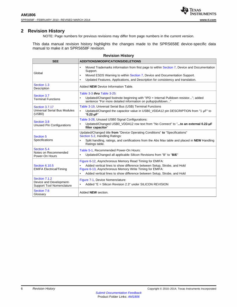
2 Revision HistoryNOTE: Page numbers for previous revisions may differ from page numbers in the current version.
This data manual revision history highlights the changes made to the SPRS658E device-specific datamanual to make it an SPRS658F revision.
Revision HistorySEE ADDITIONS/MODIFICATIONS/DELETIONS
• Moved Trademarks information from first page to within Section 7, Device and DocumentationSupport.
Global• Moved ESDS Warning to within Section 7, Device and Documentation Support.• Updated Features, Applications, and Description for consistency and translation.
Section 1.3 Added NEW Device Information Table.DescriptionTable 3-3 thru Table 3-25:
Section 3.7• Updated/Changed footnote beginning with "IPD = Internal Pulldown resistor..."; addedTerminal Functions
sentence "For more detailed information on pullup/pulldown..."Table 3-19, Universal Serial Bus (USB) Terminal FunctionsSection 3.7.17
Universal Serial Bus Modules • Updated/Changed the capacitor value in USB0_VDDA12 pin DESCRIPTION from "1 μF" to(USB0) "0.22-μF"
Table 3-28, Unused USB0 Signal Configurations:Section 3.8
• Updated/Changed USB0_VDDA12 row text from "No Connect" to "...to an external 0.22-μFUnused Pin Configurationsfilter capacitor"
Updated/Changed title from "Device Operating Conditions" to "Specifications"Section 5.2, Handling Ratings:Section 5
Specifications • Split handling, ratings, and certifications from the Abs Max table and placed in NEW HandlingRatings table.
Section 5.4 Table 5-1, Recommended Power-On Hours:Notes on Recommended
• Updated/Changed all applicable Silicon Revisions from "B" to "B/E"Power-On HoursFigure 6-12, Asynchronous Memory Read Timing for EMIFA:
Section 6.10.5 • Added vertical lines to show difference between Setup, Strobe, and HoldEMIFA Electrical/Timing Figure 6-13, Asynchronous Memory Write Timing for EMIFA:
• Added vertical lines to show difference between Setup, Strobe, and HoldSection 7.1.2 Figure 7-1, Device Nomenclature:Device and Development-
• Added "E = Silicon Revision 2.3" under SILICON REVISIONSupport Tool NomenclatureSection 7.6 Added NEW section.Glossary
6 Revision History Copyright © 2010–2014, Texas Instruments IncorporatedSubmit Documentation Feedback
Product Folder Links: AM1806
AM1806www.ti.com SPRS658F –FEBRUARY 2010–REVISED MARCH 2014
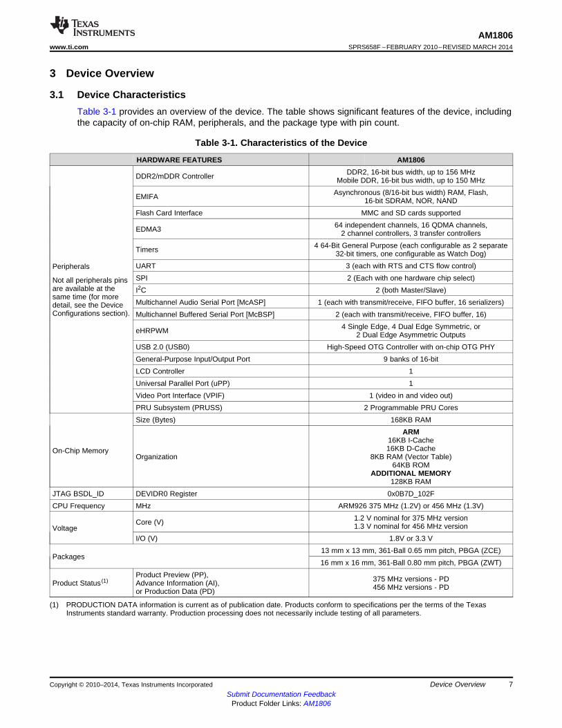
3 Device Overview
3.1 Device CharacteristicsTable 3-1 provides an overview of the device. The table shows significant features of the device, includingthe capacity of on-chip RAM, peripherals, and the package type with pin count.
Table 3-1. Characteristics of the Device
HARDWARE FEATURES AM1806DDR2, 16-bit bus width, up to 156 MHzDDR2/mDDR Controller Mobile DDR, 16-bit bus width, up to 150 MHz
Asynchronous (8/16-bit bus width) RAM, Flash,EMIFA 16-bit SDRAM, NOR, NANDFlash Card Interface MMC and SD cards supported
64 independent channels, 16 QDMA channels,EDMA3 2 channel controllers, 3 transfer controllers4 64-Bit General Purpose (each configurable as 2 separateTimers 32-bit timers, one configurable as Watch Dog)
UART 3 (each with RTS and CTS flow control)PeripheralsSPI 2 (Each with one hardware chip select)Not all peripherals pins
are available at the I2C 2 (both Master/Slave)same time (for more
Multichannel Audio Serial Port [McASP] 1 (each with transmit/receive, FIFO buffer, 16 serializers)detail, see the DeviceConfigurations section). Multichannel Buffered Serial Port [McBSP] 2 (each with transmit/receive, FIFO buffer, 16)
4 Single Edge, 4 Dual Edge Symmetric, oreHRPWM 2 Dual Edge Asymmetric OutputsUSB 2.0 (USB0) High-Speed OTG Controller with on-chip OTG PHYGeneral-Purpose Input/Output Port 9 banks of 16-bitLCD Controller 1Universal Parallel Port (uPP) 1Video Port Interface (VPIF) 1 (video in and video out)PRU Subsystem (PRUSS) 2 Programmable PRU CoresSize (Bytes) 168KB RAM
ARM16KB I-Cache16KB D-CacheOn-Chip Memory
Organization 8KB RAM (Vector Table)64KB ROM
ADDITIONAL MEMORY128KB RAM
JTAG BSDL_ID DEVIDR0 Register 0x0B7D_102FCPU Frequency MHz ARM926 375 MHz (1.2V) or 456 MHz (1.3V)
1.2 V nominal for 375 MHz versionCore (V) 1.3 V nominal for 456 MHz versionVoltageI/O (V) 1.8V or 3.3 V
13 mm x 13 mm, 361-Ball 0.65 mm pitch, PBGA (ZCE)Packages
16 mm x 16 mm, 361-Ball 0.80 mm pitch, PBGA (ZWT)Product Preview (PP), 375 MHz versions - PDProduct Status (1) Advance Information (AI), 456 MHz versions - PDor Production Data (PD)
(1) PRODUCTION DATA information is current as of publication date. Products conform to specifications per the terms of the TexasInstruments standard warranty. Production processing does not necessarily include testing of all parameters.
Copyright © 2010–2014, Texas Instruments Incorporated Device Overview 7Submit Documentation Feedback
Product Folder Links: AM1806
AM1806SPRS658F –FEBRUARY 2010–REVISED MARCH 2014 www.ti.com
3.2 Device CompatibilityThe ARM926EJ-S RISC CPU is compatible with other ARM9 CPUs from ARM Holdings plc.
3.3 ARM SubsystemThe ARM Subsystem includes the following features:• ARM926EJ-S RISC processor• ARMv5TEJ (32/16-bit) instruction set• Little endian• System Control Co-Processor 15 (CP15)• MMU• 16KB Instruction cache• 16KB Data cache• Write Buffer• Embedded Trace Module and Embedded Trace Buffer (ETM/ETB)• ARM Interrupt controller
3.3.1 ARM926EJ-S RISC CPUThe ARM Subsystem integrates the ARM926EJ-S processor. The ARM926EJ-S processor is a member ofARM9 family of general-purpose microprocessors. This processor is targeted at multi-tasking applicationswhere full memory management, high performance, low die size, and low power are all important. TheARM926EJ-S processor supports the 32-bit ARM and 16 bit THUMB instruction sets, enabling the user totrade off between high performance and high code density. Specifically, the ARM926EJ-S processorsupports the ARMv5TEJ instruction set, which includes features for efficient execution of Java byte codes,providing Java performance similar to Just in Time (JIT) Java interpreter, but without associated codeoverhead.
The ARM926EJ-S processor supports the ARM debug architecture and includes logic to assist in bothhardware and software debug. The ARM926EJ-S processor has a Harvard architecture and provides acomplete high performance subsystem, including:• ARM926EJ -S integer core• CP15 system control coprocessor• Memory Management Unit (MMU)• Separate instruction and data caches• Write buffer• Separate instruction and data (internal RAM) interfaces• Separate instruction and data AHB bus interfaces• Embedded Trace Module and Embedded Trace Buffer (ETM/ETB)
For more complete details on the ARM9, refer to the ARM926EJ-S Technical Reference Manual, availableat http://www.arm.com
3.3.2 CP15The ARM926EJ-S system control coprocessor (CP15) is used to configure and control instruction anddata caches, Memory Management Unit (MMU), and other ARM subsystem functions. The CP15 registersare programmed using the MRC and MCR ARM instructions, when the ARM in a privileged mode such assupervisor or system mode.
8 Device Overview Copyright © 2010–2014, Texas Instruments IncorporatedSubmit Documentation Feedback
Product Folder Links: AM1806
AM1806www.ti.com SPRS658F –FEBRUARY 2010–REVISED MARCH 2014
3.3.3 MMUA single set of two level page tables stored in main memory is used to control the address translation,permission checks and memory region attributes for both data and instruction accesses. The MMU uses asingle unified Translation Lookaside Buffer (TLB) to cache the information held in the page tables. TheMMU features are:• Standard ARM architecture v4 and v5 MMU mapping sizes, domains and access protection scheme.• Mapping sizes are:
– 1MB (sections)– 64KB (large pages)– 4KB (small pages)– 1KB (tiny pages)
• Access permissions for large pages and small pages can be specified separately for each quarter ofthe page (subpage permissions)
• Hardware page table walks• Invalidate entire TLB, using CP15 register 8• Invalidate TLB entry, selected by MVA, using CP15 register 8• Lockdown of TLB entries, using CP15 register 10
3.3.4 Caches and Write BufferThe size of the Instruction cache is 16KB, Data cache is 16KB. Additionally, the caches have the followingfeatures:• Virtual index, virtual tag, and addressed using the Modified Virtual Address (MVA)• Four-way set associative, with a cache line length of eight words per line (32-bytes per line) and with
two dirty bits in the Dcache• Dcache supports write-through and write-back (or copy back) cache operation, selected by memory
region using the C and B bits in the MMU translation tables• Critical-word first cache refilling• Cache lockdown registers enable control over which cache ways are used for allocation on a line fill,
providing a mechanism for both lockdown, and controlling cache corruption• Dcache stores the Physical Address TAG (PA TAG) corresponding to each Dcache entry in the TAG
RAM for use during the cache line write-backs, in addition to the Virtual Address TAG stored in theTAG RAM. This means that the MMU is not involved in Dcache write-back operations, removing thepossibility of TLB misses related to the write-back address.
• Cache maintenance operations provide efficient invalidation of, the entire Dcache or Icache, regions ofthe Dcache or Icache, and regions of virtual memory.
The write buffer is used for all writes to a noncachable bufferable region, write-through region and writemisses to a write-back region. A separate buffer is incorporated in the Dcache for holding write-back forcache line evictions or cleaning of dirty cache lines. The main write buffer has 16-word data buffer and afour-address buffer. The Dcache write-back has eight data word entries and a single address entry.
3.3.5 Advanced High-Performance Bus (AHB)The ARM Subsystem uses the AHB port of the ARM926EJ-S to connect the ARM to the Config bus andthe external memories. Arbiters are employed to arbitrate access to the separate D-AHB and I-AHB by theConfig Bus and the external memories bus.
Copyright © 2010–2014, Texas Instruments Incorporated Device Overview 9Submit Documentation Feedback
Product Folder Links: AM1806
AM1806SPRS658F –FEBRUARY 2010–REVISED MARCH 2014 www.ti.com
3.3.6 Embedded Trace Macrocell (ETM) and Embedded Trace Buffer (ETB)To support real-time trace, the ARM926EJ-S processor provides an interface to enable connection of anEmbedded Trace Macrocell (ETM). The ARM926ES-J Subsystem in the device also includes theEmbedded Trace Buffer (ETB). The ETM consists of two parts:• Trace Port provides real-time trace capability for the ARM9.• Triggering facilities provide trigger resources, which include address and data comparators, counter,
and sequencers.
The device trace port is not pinned out and is instead only connected to the Embedded Trace Buffer. TheETB has a 4KB buffer memory. ETB enabled debug tools are required to read/interpret the captured tracedata.
3.3.7 ARM Memory MappingBy default the ARM has access to most on and off chip memory areas, including EMIFA, DDR2, and theadditional 128K byte on chip SRAM. Likewise almost all of the on chip peripherals are accessible to theARM by default.
To improve security and/or robustness, the device has extensive memory and peripheral protection unitswhich can be configured to limit access rights to the various on/off chip resources to specific hosts;including the ARM as well as other master peripherals. This allows the system tasks to be partitionedbetween the ARM and DSP as best suites the particular application; while enhancing the overallrobustness of the solution.
See Table 3-2 for a detailed top level device memory map that includes the ARM memory space.
10 Device Overview Copyright © 2010–2014, Texas Instruments IncorporatedSubmit Documentation Feedback
Product Folder Links: AM1806
AM1806www.ti.com SPRS658F –FEBRUARY 2010–REVISED MARCH 2014
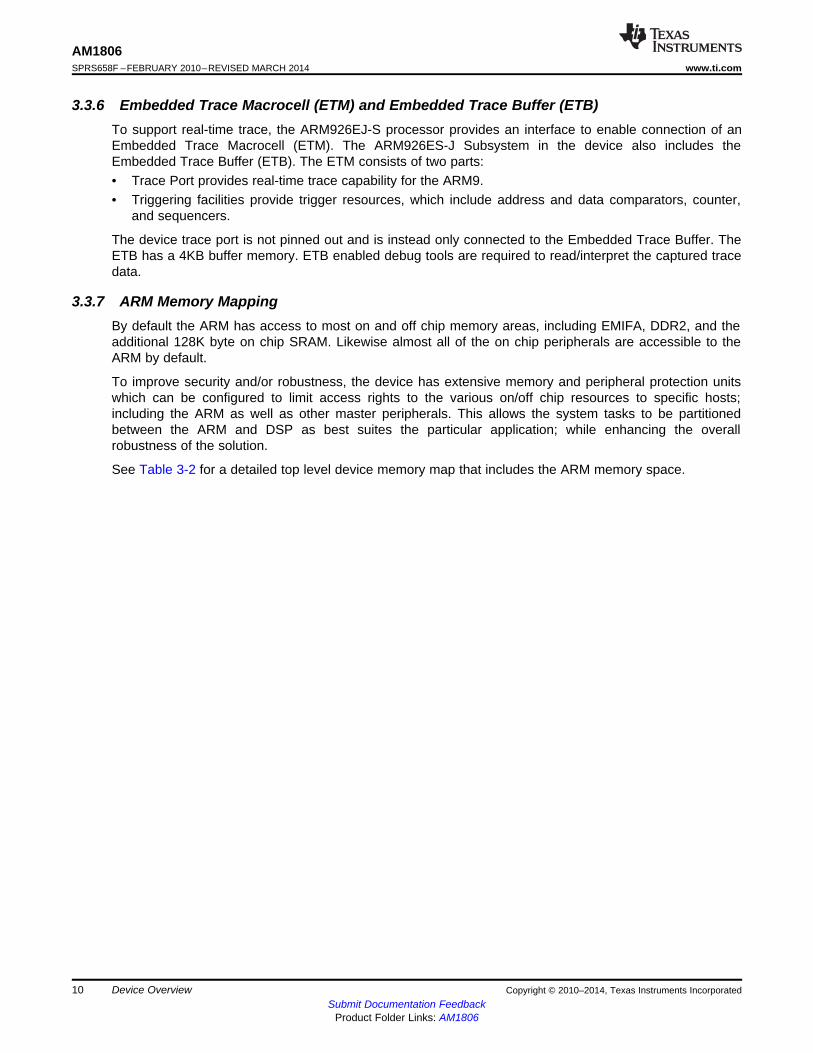
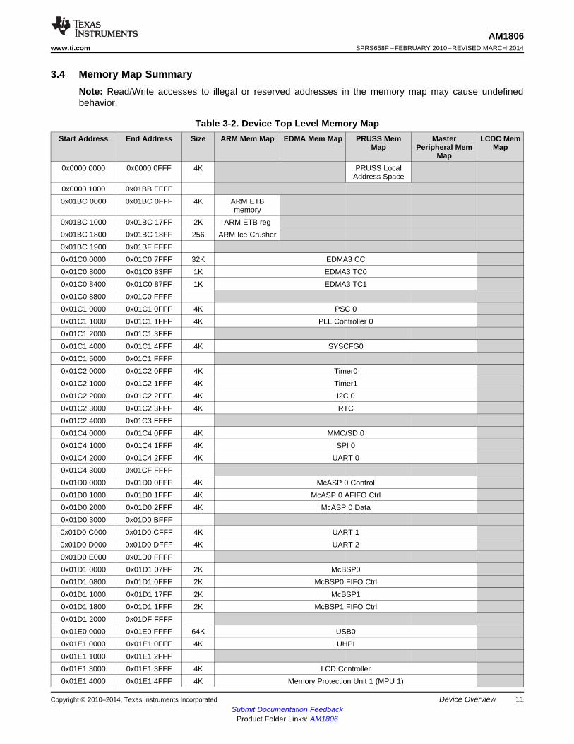
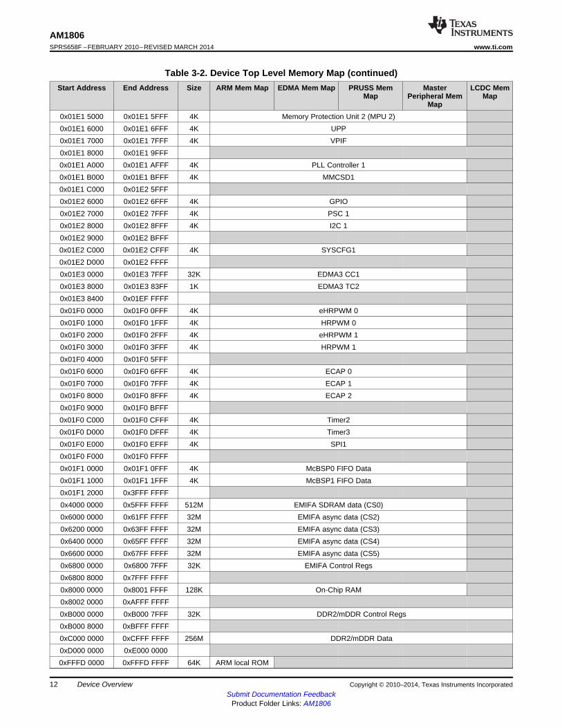
3.4 Memory Map SummaryNote: Read/Write accesses to illegal or reserved addresses in the memory map may cause undefinedbehavior.
Table 3-2. Device Top Level Memory MapStart Address End Address Size ARM Mem Map EDMA Mem Map PRUSS Mem Master LCDC Mem
Map Peripheral Mem MapMap
0x0000 0000 0x0000 0FFF 4K PRUSS LocalAddress Space
0x0000 1000 0x01BB FFFF0x01BC 0000 0x01BC 0FFF 4K ARM ETB
memory0x01BC 1000 0x01BC 17FF 2K ARM ETB reg0x01BC 1800 0x01BC 18FF 256 ARM Ice Crusher0x01BC 1900 0x01BF FFFF0x01C0 0000 0x01C0 7FFF 32K EDMA3 CC0x01C0 8000 0x01C0 83FF 1K EDMA3 TC00x01C0 8400 0x01C0 87FF 1K EDMA3 TC10x01C0 8800 0x01C0 FFFF0x01C1 0000 0x01C1 0FFF 4K PSC 00x01C1 1000 0x01C1 1FFF 4K PLL Controller 00x01C1 2000 0x01C1 3FFF0x01C1 4000 0x01C1 4FFF 4K SYSCFG00x01C1 5000 0x01C1 FFFF0x01C2 0000 0x01C2 0FFF 4K Timer00x01C2 1000 0x01C2 1FFF 4K Timer10x01C2 2000 0x01C2 2FFF 4K I2C 00x01C2 3000 0x01C2 3FFF 4K RTC0x01C2 4000 0x01C3 FFFF0x01C4 0000 0x01C4 0FFF 4K MMC/SD 00x01C4 1000 0x01C4 1FFF 4K SPI 00x01C4 2000 0x01C4 2FFF 4K UART 00x01C4 3000 0x01CF FFFF0x01D0 0000 0x01D0 0FFF 4K McASP 0 Control0x01D0 1000 0x01D0 1FFF 4K McASP 0 AFIFO Ctrl0x01D0 2000 0x01D0 2FFF 4K McASP 0 Data0x01D0 3000 0x01D0 BFFF0x01D0 C000 0x01D0 CFFF 4K UART 10x01D0 D000 0x01D0 DFFF 4K UART 20x01D0 E000 0x01D0 FFFF0x01D1 0000 0x01D1 07FF 2K McBSP00x01D1 0800 0x01D1 0FFF 2K McBSP0 FIFO Ctrl0x01D1 1000 0x01D1 17FF 2K McBSP10x01D1 1800 0x01D1 1FFF 2K McBSP1 FIFO Ctrl0x01D1 2000 0x01DF FFFF0x01E0 0000 0x01E0 FFFF 64K USB00x01E1 0000 0x01E1 0FFF 4K UHPI0x01E1 1000 0x01E1 2FFF0x01E1 3000 0x01E1 3FFF 4K LCD Controller0x01E1 4000 0x01E1 4FFF 4K Memory Protection Unit 1 (MPU 1)
Copyright © 2010–2014, Texas Instruments Incorporated Device Overview 11Submit Documentation Feedback
Product Folder Links: AM1806
AM1806SPRS658F –FEBRUARY 2010–REVISED MARCH 2014 www.ti.com
Table 3-2. Device Top Level Memory Map (continued)Start Address End Address Size ARM Mem Map EDMA Mem Map PRUSS Mem Master LCDC Mem
Map Peripheral Mem MapMap
0x01E1 5000 0x01E1 5FFF 4K Memory Protection Unit 2 (MPU 2)0x01E1 6000 0x01E1 6FFF 4K UPP0x01E1 7000 0x01E1 7FFF 4K VPIF0x01E1 8000 0x01E1 9FFF0x01E1 A000 0x01E1 AFFF 4K PLL Controller 10x01E1 B000 0x01E1 BFFF 4K MMCSD10x01E1 C000 0x01E2 5FFF0x01E2 6000 0x01E2 6FFF 4K GPIO0x01E2 7000 0x01E2 7FFF 4K PSC 10x01E2 8000 0x01E2 8FFF 4K I2C 10x01E2 9000 0x01E2 BFFF0x01E2 C000 0x01E2 CFFF 4K SYSCFG10x01E2 D000 0x01E2 FFFF0x01E3 0000 0x01E3 7FFF 32K EDMA3 CC10x01E3 8000 0x01E3 83FF 1K EDMA3 TC20x01E3 8400 0x01EF FFFF0x01F0 0000 0x01F0 0FFF 4K eHRPWM 00x01F0 1000 0x01F0 1FFF 4K HRPWM 00x01F0 2000 0x01F0 2FFF 4K eHRPWM 10x01F0 3000 0x01F0 3FFF 4K HRPWM 10x01F0 4000 0x01F0 5FFF0x01F0 6000 0x01F0 6FFF 4K ECAP 00x01F0 7000 0x01F0 7FFF 4K ECAP 10x01F0 8000 0x01F0 8FFF 4K ECAP 20x01F0 9000 0x01F0 BFFF0x01F0 C000 0x01F0 CFFF 4K Timer20x01F0 D000 0x01F0 DFFF 4K Timer30x01F0 E000 0x01F0 EFFF 4K SPI10x01F0 F000 0x01F0 FFFF0x01F1 0000 0x01F1 0FFF 4K McBSP0 FIFO Data0x01F1 1000 0x01F1 1FFF 4K McBSP1 FIFO Data0x01F1 2000 0x3FFF FFFF0x4000 0000 0x5FFF FFFF 512M EMIFA SDRAM data (CS0)0x6000 0000 0x61FF FFFF 32M EMIFA async data (CS2)0x6200 0000 0x63FF FFFF 32M EMIFA async data (CS3)0x6400 0000 0x65FF FFFF 32M EMIFA async data (CS4)0x6600 0000 0x67FF FFFF 32M EMIFA async data (CS5)0x6800 0000 0x6800 7FFF 32K EMIFA Control Regs0x6800 8000 0x7FFF FFFF0x8000 0000 0x8001 FFFF 128K On-Chip RAM0x8002 0000 0xAFFF FFFF0xB000 0000 0xB000 7FFF 32K DDR2/mDDR Control Regs0xB000 8000 0xBFFF FFFF0xC000 0000 0xCFFF FFFF 256M DDR2/mDDR Data0xD000 0000 0xE000 00000xFFFD 0000 0xFFFD FFFF 64K ARM local ROM
12 Device Overview Copyright © 2010–2014, Texas Instruments IncorporatedSubmit Documentation Feedback
Product Folder Links: AM1806
AM1806www.ti.com SPRS658F –FEBRUARY 2010–REVISED MARCH 2014
Table 3-2. Device Top Level Memory Map (continued)Start Address End Address Size ARM Mem Map EDMA Mem Map PRUSS Mem Master LCDC Mem
Map Peripheral Mem MapMap
0xFFFE 0000 0xFFFE DFFF0xFFFE E000 0xFFFE FFFF 8K ARM Interrupt
Controller0xFFFF 0000 0xFFFF 1FFF 8K ARM local RAM ARM Local RAM
(PRU0 only)0xFFFF 2000 0xFFFF FFFF
Copyright © 2010–2014, Texas Instruments Incorporated Device Overview 13Submit Documentation Feedback
Product Folder Links: AM1806
W
V
U
T
R
P
N
M
L
K
10987654321
10987654321
DVDD3318_C
VP_CLKOUT3/PRU1_R30[0]/
GP6[1]/PRU1_R31[1]
VSS
NC
VP_CLKOUT2/MMCSD1_DAT[2]/
PRU1_R30[2]/GP6[3]/
PRU1_R31[3]
NC
NC
NC NCNC NC
NC NCNC
DVDD3318_C
DDR_A[11]
VP_DOUT[15]/LCD_D[15]/UPP_XD[7]/
GP7[7]/BOOT[7]
DVDD3318_C
DVDD18
DDR_DVDD18 DDR_DVDD18
DDR_D[15]DDR_RASDDR_CLKPDDR_CLKNDDR_A[2]DDR_A[10]
VSS
LCD_AC_ENB_CS/GP6[0]/
PRU1_R31[28]
DDR_A[13]
DDR_CAS
DDR_A[5] DDR_CKE DDR_BA[0]
VSS
CVDDRVDD
DDR_A[9] DDR_A[1] DDR_WE DDR_D[10]
DDR_A[7] DDR_A[0] DDR_D[12]
DDR_A[12] DDR_A[3] DDR_CS
DDR_A[6]
DDR_DQM[1]
VSS CVDD
VSS
DDR_DVDD18
VP_DOUT[12]/LCD_D[12]/UPP_XD[4]/
GP7[4]/BOOT[4]
DDR_VREF
DDR_BA[1]
DDR_A[8] DDR_A[4] DDR_BA[2]
VSS
W
V
U
T
R
P
N
M
L
K
DDR_D[13]
VSS VSS VSS
VSS DVDD18 VSS VSS VSS VSS
NC VSS VSS VSS VSS CVDD CVDD VSS
DDR_DVDD18DDR_DVDD18DDR_DVDD18DDR_DVDD18DVDD3318_C
VP_DOUT[13]/LCD_D[13]/UPP_XD[5]/
GP7[5]/BOOT[5]
VP_DOUT[14]/LCD_D[14]/UPP_XD[6]/
GP7[6]/BOOT[6]
DDR_DVDD18 DDR_DVDD18 DDR_DVDD18
VP_DOUT[9]/LCD_D[9]/
UPP_XD[1]/GP7[1]/BOOT[1]
VP_DOUT[10]/LCD_D[10]/UPP_XD[2]/
GP7[2]/BOOT[2]
VP_DOUT[11]/LCD_D[11]/UPP_XD[3]/
GP7[3]/BOOT[3]
VP_DOUT[6]/LCD_D[6]/
UPP_XD[14]/GP7[14]/
PRU1_R31[14]
VP_DOUT[7]/LCD_D[7]/
UPP_XD[15]/GP7[15]/
PRU1_R31[15]
VP_DOUT[8]/LCD_D[8]/
UPP_XD[0]/GP7[0]/BOOT[0]
VP_DOUT[3]/LCD_D[3]/
UPP_XD[11]/GP7[11]/
PRU1_R31[11]
VP_DOUT[4]/LCD_D[4]/
UPP_XD[12]/GP7[12]/
PRU1_R31[12]
VP_DOUT[5]/LCD_D[5]/
UPP_XD[13]/GP7[13]/
PRU1_R31[13]
VP_DOUT[0]/LCD_D[0]/
UPP_XD[8]/GP7[8]/
PRU1_R31[8]
VP_DOUT[1]/LCD_D[1]/
UPP_XD[9]/GP7[9]/
PRU1_R31[9]
VP_DOUT[2]/LCD_D[2]/
UPP_XD[10]/GP7[10]/
PRU1_R31[10]
A B
CD
AM1806SPRS658F –FEBRUARY 2010–REVISED MARCH 2014 www.ti.com
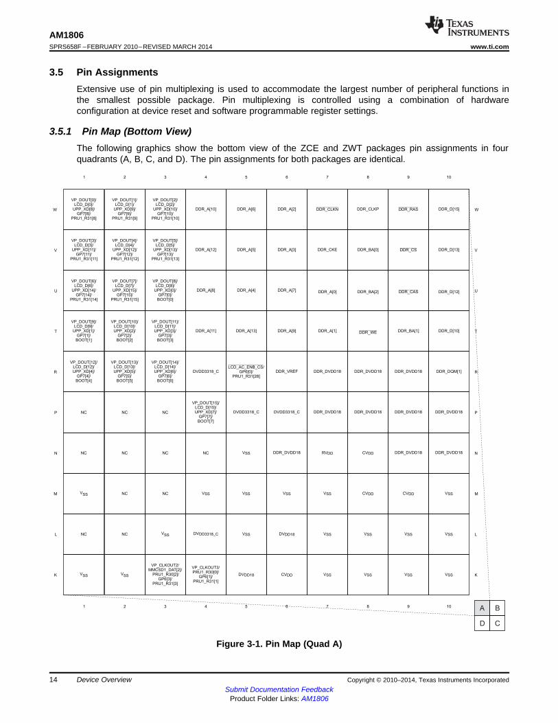
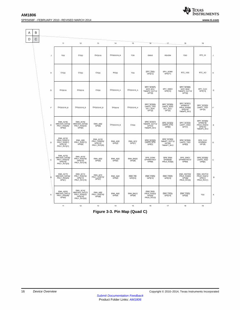
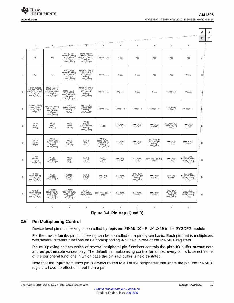
3.5 Pin AssignmentsExtensive use of pin multiplexing is used to accommodate the largest number of peripheral functions inthe smallest possible package. Pin multiplexing is controlled using a combination of hardwareconfiguration at device reset and software programmable register settings.
3.5.1 Pin Map (Bottom View)The following graphics show the bottom view of the ZCE and ZWT packages pin assignments in fourquadrants (A, B, C, and D). The pin assignments for both packages are identical.
Figure 3-1. Pin Map (Quad A)
14 Device Overview Copyright © 2010–2014, Texas Instruments IncorporatedSubmit Documentation Feedback
Product Folder Links: AM1806

W
V
U
T
R
P
N
M
L
K
191817161514131211
191817161514131211
NC
DVDD3318_CCVDD
USB_CVDD
DVDD3318_C
DDR_DQGATE0 DVDD18DDR_DQGATE1
DDR_D[9] DDR_D[8]DDR_D[11]
DVDD18
RTC_CVDD
RESET
USB0_DM USB0_DP
VP_DIN[11]/UHPI_HD[3]/UPP_D[3]/
PRU0_R30[11]/PRU0_R31[11]
USB0_VDDA33 USB0_VBUS
NC
VP_DIN[0]/UHPI_HD[8]/UPP_D[8]/
PRU1_R31[29]
VP_DIN[1]/UHPI_HD[9]/UPP_D[9]/
PRU0_R31[23]
VP_DIN[2]/UHPI_HD[10]/UPP_D[10]/
PRU0_R31[24]
VP_DIN[4]/UHPI_HD[12]/UPP_D[12]/
PRU0_R31[26]
PRU0_R30[28]/UHPI_HCNTL1/
UPP_CHA_START/GP6[10]
NC
PLL0_VDDA
PRU0_R30[30] //
PRU1_R30[11]/GP6[12]
UHPI_HINT
USB0_VDDA18
VP_DIN[5]/UHPI_HD[13]/UPP_D[13]/
PRU0_R31[27]
DDR_D[1]
VP_DIN[7]/UHPI_HD[15]/UPP_D[15]/
PRU0_R31[29]
OSCVSS
DDR_D[2]
VP_DIN[6]/UHPI_HD[14]/UPP_D[14]/
PRU0_R31[28]
VP_DIN[3]/UHPI_HD[11]/UPP_D[11]/
PRU0_R31[25]
VP_DIN[14]_HSYNC/
UHPI_HD[6]/UPP_D[6]/
PRU0_R30[14]/PRU0_R31[14]
EMU1
VP_DIN[8]/UHPI_HD[0]/UPP_D[0]/
GP6[5]/PRU1_R31[0]
USB0_VDDA12
TDI
NC
PRU0_R30[26]/UHPI_HR /
UPP_CHA_WAIT/GP6[8]/
PRU1_R31[17]
WVP_DIN[12]/UHPI_HD[4]/UPP_D[4]/
PRU0_R30[12]/PRU0_R31[12]
RESETOUTUHPI_HAS
//
PRU1_R30[14]/GP6[15]
RSV2
RTCK/GP8[0]
OSCOUT
DDR_D[0]
PRU0_R30[27]/UHPI_HHWIL/
UPP_CHA_ENABLE/GP6[9]
VP_DIN[13]_FIELD/
UHPI_HD[5]/UPP_D[5]/
PRU0_R30[13]/PRU0_R31[13]
TRST OSCIN
VP_CLKIN1//
PRU1_R30[9]/GP6[6]/
PRU1_R31[16]
UHPI_HDS1
VP_DIN[15]_VSYNC/
UHPI_HD[7]/UPP_D[7]/
PRU0_R30[15]/PRU0_R31[15]
VP_CLKIN0//
PRU1_R30[10]/GP6[7]/
UPP_2xTXCLK
UHPI_HCS
VP_DIN[10]/UHPI_HD[2]/UPP_D[2]/
PRU0_R30[10]/PRU0_R31[10]
VSS DVDD3318_B
PLL0_VSSA
TMS
PRU0_R30[31]//
PRU1_R30[12]GP6[13]
UHPI_HRDY
NC PLL1_VSSA
PLL1_VDDA
NC USB0_ID
VP_DIN[9]/UHPI_HD[1]/UPP_D[1]/
PRU0_R30[9]/PRU0_R31[9]
CLKOUT//
PRU1_R30[13]/GP6[14]
UHPI_HDS2
USB0_DRVVBUS
DDR_DQS[0]
PRU0_R30[29]/UHPI_HCNTL0/
UPP_CHA_CLOCK/GP6[11]
W
V
U
T
R
P
N
M
L
K
DDR_DQM[0]
DDR_D[3]
DDR_D[4]
DDR_D[6]
DDR_ZP
DDR_D[5]
DDR_D[7]
DDR_D[14]
DDR_DQS[1]
VSS
VSS
VSS
VSS
VSS
CVDD DVDD3318_C
DVDD3318_C
DVDD3318_C
A B
CD
AM1806www.ti.com SPRS658F –FEBRUARY 2010–REVISED MARCH 2014
Figure 3-2. Pin Map (Quad B)
Copyright © 2010–2014, Texas Instruments Incorporated Device Overview 15Submit Documentation Feedback
Product Folder Links: AM1806
H
G
F
E
D
C
B
A
191817161514131211
191817161514131211
CVDD
EMA_A[8]/PRU1_R30[16]/
GP5[8]
EMA_A[14]/MMCSD0_DAT[7]/
PRU1_R30[22]/GP5[14]/
PRU1_R31[22]
EMA_A[15]/MMCSD0_DAT[6]/
PRU1_R30[23]/GP5[15]/
PRU1_R31[23]
EMA_A[10]/PRU1_R30[18]/
GP5[10]/PRU1_R31[18]
EMA_A[9]/PRU1_R30[17]/
GP5[9]
EMA_A[13]/PRU0_R30[21]/PRU1_R30[21]
GP5[13]/PRU1_R31[21]
EMA_A[12]/PRU1_R30[20]/
GP5[12]/PRU1_R31[20]
EMA_A[16]/MMCSD0_DAT[5]/
PRU1_R30[24]/GP4[0]
EMA_A[18]/MMCSD0_DAT[3]/
PRU1_R30[26]/GP4[2]
DVDD3318_B
DVDD18
EMA_A[6]/GP5[6]
EMA_A[5]/GP5[5]
EMA_A[2]/GP5[2]
EMA_A[7]/PRU1_R30[15]/
GP5[7]
EMA_A[4]/GP5[4]
SPI0_SIMO/EPWMSYNCO/
GP8[5]
SPI0_SCS[5]/UART0_RXD/
GP8[4]
SPI1_SCS[1]/EPWM1A/
PRU0_R30[8]/GP2[15]/
TM64P2_IN12
SPI0_SCS[4]/UART0_TXD/
GP8[3]
SPI0_CLK/EPWM0A/
GP1[8]
SPI1_SCS[3]/UART1_RXD/
GP1[1]
SPI1_SCS[0]/EPWM1B/
PRU0_R30[7]/GP2[14]/
TM64P3_IN12
EMA_OE/GP3[10]
SPI1_SCS[4]/UART2_TXD/I2C1_SDA/
GP1[2]
EMA_A[3]/GP5[3]
DVDD18
RTC_VSS
EMA_WAIT[0]/PRU0_R30[0]/
GP3[8]/PRU0_R31[0]
EMA_RAS/PRU0_R30[3]/
GP2[5]/PRU0_R31[3]
SPI0_SCS[3]UART0_CTS
//
GP8[2]
SPI0_SCS[0]/TM64P1_OUT12/
GP1[6]/TM64P1_IN12
SPI0_SOMI/EPWMSYNCI/
GP8[6]
SPI0_SCS[2]UART0_RTS
//
GP8[1]
SPI1_SCS[7]/I2C0_SCL/
TM64P2_OUT12/GP1[5]
SPI1_SIMO/GP2[10]
SPI1_CLK/GP2[13]
EMA_CS[3]/GP3[14]
VSS
VSSSPI1_ENA/
GP2[12]RTC_XO
EMA_CS[2]/GP3[15]
EMA_WAIT[1]/PRU0_R30[1]/
GP2[1]/PRU0_R31[1]
EMA_A[20]/MMCSD0_DAT[1]/
PRU1_R30[28]/GP4[4]
EMA_BA[1]/GP2[9]
SPI0_ENA/EPWM0B/
PRU0_R30[6]
EMA_CS[5]/GP3[12]
SPI1_SCS[5]/UART2_RXD/
I2C1_SCL/GP1[3]
EMA_A[0]/GP5[0]
EMA_BA[0]/GP2[8]
EMA_A[1]/GP5[1]
DVDD3318_B
SPI0_SCS[1]/TM64P0_OUT12/
GP1[7]/TM64P0_IN12
DVDD3318_A
SPI1_SCS[6]/I2C0_SDA/
TM64P3_OUT12/GP1[4]
EMA_CS[0]/GP2[0]
CVDDSPI1_SOMI/
GP2[11] H
G
F
E
D
C
B
A
J TDOTCK EMU0 RTC_XIRSVDN J
SPI1_SCS[2]/UART1_TXD/
GP1[0]
EMA_A[11]/PRU1_R30[19]/
GP5[11]/PRU1_R31[19]
EMA_A[17]/MMCSD0_DAT[4]/
PRU1_R30[25]GP4[1]
DVDD3318_BDVDD3318_B
DVDD18 CVDD DVDD3318_A DVDD3318_A
RVDDCVDDCVDD
VSS CVDD DVDD18 DVDD3318_B
A B
CD
AM1806SPRS658F –FEBRUARY 2010–REVISED MARCH 2014 www.ti.com
Figure 3-3. Pin Map (Quad C)
16 Device Overview Copyright © 2010–2014, Texas Instruments IncorporatedSubmit Documentation Feedback
Product Folder Links: AM1806
J
H
G
F
E
D
C
B
A
10987654321
10987654321
EMA_D[15]/GP3[7]
AXR15/EPWM0TZ[0]/
ECAP2_APWM2/GP0[7]
ACLKR/PRU0_R30[20]/
GP0[15]/PRU0_R31[22]
ACLKX/PRU0_R30[19]/
GP0[14]/PRU0_R31[21]
AHCLKX/USB_REFCLKIN/
/GP0[10]/
PRU0_R31[17]
UART1_CTS
AFSX/GP0[12]/
PRU0_R31[19]
AFSR/GP0[13]/
PRU0_R31[20]
AXR9/DX1/
GP0[1]
AXR4/FSR0/
GP1[12]
AXR5/CLKX0/GP1[13]
AXR7/EPWM1TZ[0]/PRU0_R30[17]
GP1[15]/PRU0_R31[7]
AXR10/DR1/
GP0[2]
AXR1/DX0/
GP1[9]
AXR3/FSX0/
GP1[11]
AXR2/DR0/
GP1[10]
MMCSD1_DAT[6]/LCD_MCLK/
PRU1_R30[6]/GP8[10]/
PRU1_R31[7]
RTC_ALARM//
GP0[8]/UART2_CTS
DEEPSLEEP
AXR0/ECAP0_APWM0/
GP8[7]/CLKS0
PRU0_R30[24]/MMCSD1_CLK/
UPP_CHB_START/GP8[14]/
PRU1_R31[26]
MMCSD1_DAT[4]/LCD_VSYNC/PRU1_R30[4]/
GP8[8]/PRU1_R31[5]
VSS
PRU0_R30[22]/PRU1_R30[8]/
UPP_CHB_WAIT/GP8[12]/
PRU1_R31[24]
AXR8/CLKS1/
ECAP1_APWM1/GP0[0]/
PRU0_R31[8]
AXR12/FSR1/GP0[4]
EMA_D[4]/GP4[12]
AXR14/CLKR1/GP0[6]
EMA_WEN_DQM[1]/GP2[2]
EMA_D[0]/GP4[8]
EMA_A[19]/MMCSD0_DAT[2]/
PRU1_R30[27]/GP4[3]
EMA_D[9]/GP3[1]
EMA_A_R /GP3[9]
W
MMCSD0_CLK/PRU1_R30[31]/
GP4[7]
EMA_D[8]/GP3[0]
EMA_D[13]/GP3[5]
VP_CLKIN2/MMCSD1_DAT[3]/
PRU1_R30[3]/GP6[4]/
PRU1_R31[4]
VP_CLKIN3/MMCSD1_DAT[1]/
PRU1_R30[1]/GP6[2]/
PRU1_R31[2]
AMUTE/
GP0[9]/PRU0_R31[16]
PRU0_R30[16]/UART2_RTS/
DVDD3318_A
DVDD3318_A
EMA_WE/GP3[11]
EMA_D[10]/GP3[2]
EMA_D[3]/GP4[11]
EMA_SDCKE/PRU0_R30[4]/
GP2[6]/PRU0_R31[4]
EMA_D[14]/GP3[6]
EMA_D[7]/GP4[15]
EMA_D[1]/GP4[9]
EMA_A[22]/MMCSD0_CMD/PRU1_R30[30]/
GP4[6]
EMA_D[2]/GP4[10]
EMA_A[21]/MMCSD0_DAT[0]/
PRU1_R30[29]/GP4[5]
PRU0_R30[23]/MMCSD1_CMD/
UPP_CHB_ENABLE/GP8[13]/
PRU1_R31[25]
AHCLKR/
/GP0[11]/
PRU0_R31[18]
PRU0_R30[18]/UART1_RTS
EMA_D[12]/GP3[4]
EMA_WEN_DQM[0]/GP2[3]
EMA_CLK/PRU0_R30[5]/
GP2[7]/PRU0_R31[5]
AXR6/CLKR0/GP1[14]/
PRU0_R31[6]
AXR11/FSX1/GP0[3]
EMA_D[6]/GP4[14]
EMA_D[11]/GP3[3]
RVDDEMA_D[5]/
GP4[13]
MMCSD1_DAT[7]/LCD_PCLK/
PRU1_R30[7]/GP8[11]
MMCSD1_DAT[5]/LCD_HSYNC/PRU1_R30[5]/
GP8[9]/PRU1_R31[6]
PRU0_R30[25]/MMCSD1_DAT[0]/
UPP_CHB_CLOCK/GP8[15]/
PRU1_R31[27]
AXR13/CLKX1/GP0[5]
J
H
G
F
E
D
C
B
A
EMA_CS[4]/GP3[13]
EMA_CAS/PRU0_R30[2]/
GP2[4]/PRU0_R31[2]
DVDD3318_B DVDD3318_B DVDD3318_B DVDD3318_B
DVDD18 CVDD CVDD DVDD3318_B DVDD18
VSS DVDD3318_A
VSS VSS
CVDD CVDD VSS VSS CVDD
NC NC DVDD3318_C CVDD VSS VSS
A B
CD
AM1806www.ti.com SPRS658F –FEBRUARY 2010–REVISED MARCH 2014
Figure 3-4. Pin Map (Quad D)
3.6 Pin Multiplexing ControlDevice level pin multiplexing is controlled by registers PINMUX0 - PINMUX19 in the SYSCFG module.
For the device family, pin multiplexing can be controlled on a pin-by-pin basis. Each pin that is multiplexedwith several different functions has a corresponding 4-bit field in one of the PINMUX registers.
Pin multiplexing selects which of several peripheral pin functions controls the pin's IO buffer output dataand output enable values only. The default pin multiplexing control for almost every pin is to select 'none'of the peripheral functions in which case the pin's IO buffer is held tri-stated.
Note that the input from each pin is always routed to all of the peripherals that share the pin; the PINMUXregisters have no effect on input from a pin.
Copyright © 2010–2014, Texas Instruments Incorporated Device Overview 17Submit Documentation Feedback
Product Folder Links: AM1806
AM1806SPRS658F –FEBRUARY 2010–REVISED MARCH 2014 www.ti.com
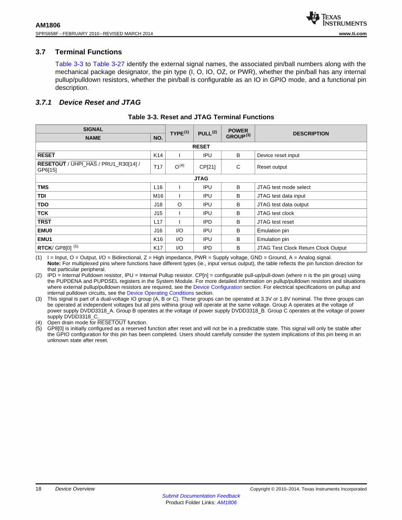
3.7 Terminal FunctionsTable 3-3 to Table 3-27 identify the external signal names, the associated pin/ball numbers along with themechanical package designator, the pin type (I, O, IO, OZ, or PWR), whether the pin/ball has any internalpullup/pulldown resistors, whether the pin/ball is configurable as an IO in GPIO mode, and a functional pindescription.
3.7.1 Device Reset and JTAG
Table 3-3. Reset and JTAG Terminal Functions
SIGNAL POWERTYPE (1) PULL (2) DESCRIPTIONGROUP (3)NAME NO.RESET
RESET K14 I IPU B Device reset inputRESETOUT / UHPI_HAS / PRU1_R30[14] / T17 O (4) CP[21] C Reset outputGP6[15]
JTAGTMS L16 I IPU B JTAG test mode selectTDI M16 I IPU B JTAG test data inputTDO J18 O IPU B JTAG test data outputTCK J15 I IPU B JTAG test clockTRST L17 I IPD B JTAG test resetEMU0 J16 I/O IPU B Emulation pinEMU1 K16 I/O IPU B Emulation pinRTCK/ GP8[0] (5) K17 I/O IPD B JTAG Test Clock Return Clock Output
(1) I = Input, O = Output, I/O = Bidirectional, Z = High impedance, PWR = Supply voltage, GND = Ground, A = Analog signal.Note: For multiplexed pins where functions have different types (ie., input versus output), the table reflects the pin function direction forthat particular peripheral.
(2) IPD = Internal Pulldown resistor, IPU = Internal Pullup resistor. CP[n] = configurable pull-up/pull-down (where n is the pin group) usingthe PUPDENA and PUPDSEL registers in the System Module. For more detailed information on pullup/pulldown resistors and situationswhere external pullup/pulldown resistors are required, see the Device Configuration section. For electrical specifications on pullup andinternal pulldown circuits, see the Device Operating Conditions section.
(3) This signal is part of a dual-voltage IO group (A, B or C). These groups can be operated at 3.3V or 1.8V nominal. The three groups canbe operated at independent voltages but all pins withina group will operate at the same voltage. Group A operates at the voltage ofpower supply DVDD3318_A. Group B operates at the voltage of power supply DVDD3318_B. Group C operates at the voltage of powersupply DVDD3318_C.
(4) Open drain mode for RESETOUT function.(5) GP8[0] is initially configured as a reserved function after reset and will not be in a predictable state. This signal will only be stable after
the GPIO configuration for this pin has been completed. Users should carefully consider the system implications of this pin being in anunknown state after reset.
18 Device Overview Copyright © 2010–2014, Texas Instruments IncorporatedSubmit Documentation Feedback
Product Folder Links: AM1806
AM1806www.ti.com SPRS658F –FEBRUARY 2010–REVISED MARCH 2014
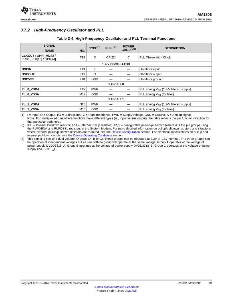
3.7.2 High-Frequency Oscillator and PLL
Table 3-4. High-Frequency Oscillator and PLL Terminal Functions
SIGNAL POWERTYPE (1) PULL (2) DESCRIPTIONGROUP (3)NAME NO.CLKOUT / UHPI_HDS2 / T18 O CP[22] C PLL Observation ClockPRU1_R30[13] / GP6[14]
1.2-V OSCILLATOROSCIN L19 I — — Oscillator inputOSCOUT K19 O — — Oscillator outputOSCVSS L18 GND — — Oscillator ground
1.2-V PLL0PLL0_VDDA L15 PWR — — PLL analog VDD (1.2-V filtered supply)PLL0_VSSA M17 GND — — PLL analog VSS (for filter)
1.2-V PLL1PLL1_VDDA N15 PWR — — PLL analog VDD (1.2-V filtered supply)PLL1_VSSA M15 GND — — PLL analog VSS (for filter)
(1) I = Input, O = Output, I/O = Bidirectional, Z = High impedance, PWR = Supply voltage, GND = Ground, A = Analog signal.Note: For multiplexed pins where functions have different types (ie., input versus output), the table reflects the pin function direction forthat particular peripheral.
(2) IPD = Internal Pulldown resistor; IPU = Internal Pullup resistor; CP[n] = configurable pull-up/pull-down (where n is the pin group) usingthe PUPDENA and PUPDSEL registers in the System Module. For more detailed information on pullup/pulldown resistors and situationswhere external pullup/pulldown resistors are required, see the Device Configuration section. For electrical specifications on pullup andinternal pulldown circuits, see the Device Operating Conditions section.
(3) This signal is part of a dual-voltage IO group (A, B or C). These groups can be operated at 3.3V or 1.8V nominal. The three groups canbe operated at independent voltages but all pins withina group will operate at the same voltage. Group A operates at the voltage ofpower supply DVDD3318_A. Group B operates at the voltage of power supply DVDD3318_B. Group C operates at the voltage of powersupply DVDD3318_C.
Copyright © 2010–2014, Texas Instruments Incorporated Device Overview 19Submit Documentation Feedback
Product Folder Links: AM1806
AM1806SPRS658F –FEBRUARY 2010–REVISED MARCH 2014 www.ti.com
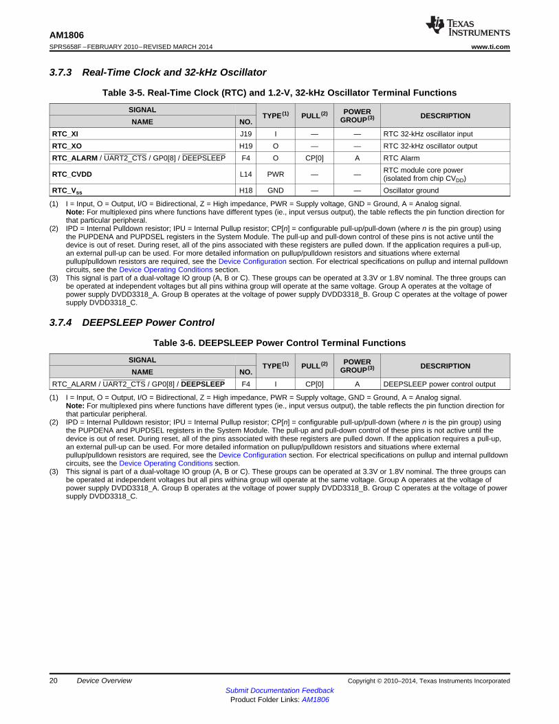
3.7.3 Real-Time Clock and 32-kHz Oscillator
Table 3-5. Real-Time Clock (RTC) and 1.2-V, 32-kHz Oscillator Terminal Functions
SIGNAL POWERTYPE (1) PULL (2) DESCRIPTIONGROUP (3)NAME NO.RTC_XI J19 I — — RTC 32-kHz oscillator inputRTC_XO H19 O — — RTC 32-kHz oscillator outputRTC_ALARM / UART2_CTS / GP0[8] / DEEPSLEEP F4 O CP[0] A RTC Alarm
RTC module core powerRTC_CVDD L14 PWR — — (isolated from chip CVDD)RTC_Vss H18 GND — — Oscillator ground
(1) I = Input, O = Output, I/O = Bidirectional, Z = High impedance, PWR = Supply voltage, GND = Ground, A = Analog signal.Note: For multiplexed pins where functions have different types (ie., input versus output), the table reflects the pin function direction forthat particular peripheral.
(2) IPD = Internal Pulldown resistor; IPU = Internal Pullup resistor; CP[n] = configurable pull-up/pull-down (where n is the pin group) usingthe PUPDENA and PUPDSEL registers in the System Module. The pull-up and pull-down control of these pins is not active until thedevice is out of reset. During reset, all of the pins associated with these registers are pulled down. If the application requires a pull-up,an external pull-up can be used. For more detailed information on pullup/pulldown resistors and situations where externalpullup/pulldown resistors are required, see the Device Configuration section. For electrical specifications on pullup and internal pulldowncircuits, see the Device Operating Conditions section.
(3) This signal is part of a dual-voltage IO group (A, B or C). These groups can be operated at 3.3V or 1.8V nominal. The three groups canbe operated at independent voltages but all pins withina group will operate at the same voltage. Group A operates at the voltage ofpower supply DVDD3318_A. Group B operates at the voltage of power supply DVDD3318_B. Group C operates at the voltage of powersupply DVDD3318_C.
3.7.4 DEEPSLEEP Power Control
Table 3-6. DEEPSLEEP Power Control Terminal Functions
SIGNAL POWERTYPE (1) PULL (2) DESCRIPTIONGROUP (3)NAME NO.RTC_ALARM / UART2_CTS / GP0[8] / DEEPSLEEP F4 I CP[0] A DEEPSLEEP power control output
(1) I = Input, O = Output, I/O = Bidirectional, Z = High impedance, PWR = Supply voltage, GND = Ground, A = Analog signal.Note: For multiplexed pins where functions have different types (ie., input versus output), the table reflects the pin function direction forthat particular peripheral.
(2) IPD = Internal Pulldown resistor; IPU = Internal Pullup resistor; CP[n] = configurable pull-up/pull-down (where n is the pin group) usingthe PUPDENA and PUPDSEL registers in the System Module. The pull-up and pull-down control of these pins is not active until thedevice is out of reset. During reset, all of the pins associated with these registers are pulled down. If the application requires a pull-up,an external pull-up can be used. For more detailed information on pullup/pulldown resistors and situations where externalpullup/pulldown resistors are required, see the Device Configuration section. For electrical specifications on pullup and internal pulldowncircuits, see the Device Operating Conditions section.
(3) This signal is part of a dual-voltage IO group (A, B or C). These groups can be operated at 3.3V or 1.8V nominal. The three groups canbe operated at independent voltages but all pins withina group will operate at the same voltage. Group A operates at the voltage ofpower supply DVDD3318_A. Group B operates at the voltage of power supply DVDD3318_B. Group C operates at the voltage of powersupply DVDD3318_C.
20 Device Overview Copyright © 2010–2014, Texas Instruments IncorporatedSubmit Documentation Feedback
Product Folder Links: AM1806
AM1806www.ti.com SPRS658F –FEBRUARY 2010–REVISED MARCH 2014
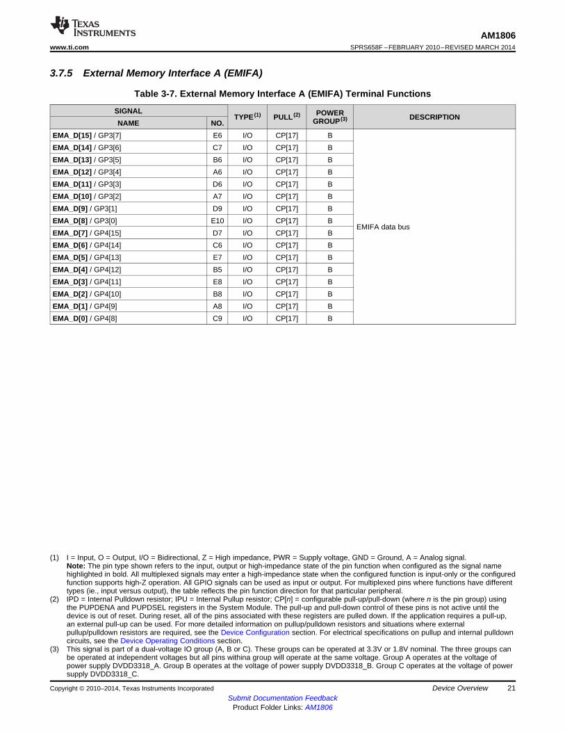
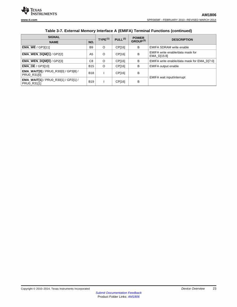
3.7.5 External Memory Interface A (EMIFA)
Table 3-7. External Memory Interface A (EMIFA) Terminal Functions
SIGNAL POWERTYPE (1) PULL (2) DESCRIPTIONGROUP (3)NAME NO.EMA_D[15] / GP3[7] E6 I/O CP[17] BEMA_D[14] / GP3[6] C7 I/O CP[17] BEMA_D[13] / GP3[5] B6 I/O CP[17] BEMA_D[12] / GP3[4] A6 I/O CP[17] BEMA_D[11] / GP3[3] D6 I/O CP[17] BEMA_D[10] / GP3[2] A7 I/O CP[17] BEMA_D[9] / GP3[1] D9 I/O CP[17] BEMA_D[8] / GP3[0] E10 I/O CP[17] B
EMIFA data busEMA_D[7] / GP4[15] D7 I/O CP[17] BEMA_D[6] / GP4[14] C6 I/O CP[17] BEMA_D[5] / GP4[13] E7 I/O CP[17] BEMA_D[4] / GP4[12] B5 I/O CP[17] BEMA_D[3] / GP4[11] E8 I/O CP[17] BEMA_D[2] / GP4[10] B8 I/O CP[17] BEMA_D[1] / GP4[9] A8 I/O CP[17] BEMA_D[0] / GP4[8] C9 I/O CP[17] B
(1) I = Input, O = Output, I/O = Bidirectional, Z = High impedance, PWR = Supply voltage, GND = Ground, A = Analog signal.Note: The pin type shown refers to the input, output or high-impedance state of the pin function when configured as the signal namehighlighted in bold. All multiplexed signals may enter a high-impedance state when the configured function is input-only or the configuredfunction supports high-Z operation. All GPIO signals can be used as input or output. For multiplexed pins where functions have differenttypes (ie., input versus output), the table reflects the pin function direction for that particular peripheral.
(2) IPD = Internal Pulldown resistor; IPU = Internal Pullup resistor; CP[n] = configurable pull-up/pull-down (where n is the pin group) usingthe PUPDENA and PUPDSEL registers in the System Module. The pull-up and pull-down control of these pins is not active until thedevice is out of reset. During reset, all of the pins associated with these registers are pulled down. If the application requires a pull-up,an external pull-up can be used. For more detailed information on pullup/pulldown resistors and situations where externalpullup/pulldown resistors are required, see the Device Configuration section. For electrical specifications on pullup and internal pulldowncircuits, see the Device Operating Conditions section.
(3) This signal is part of a dual-voltage IO group (A, B or C). These groups can be operated at 3.3V or 1.8V nominal. The three groups canbe operated at independent voltages but all pins withina group will operate at the same voltage. Group A operates at the voltage ofpower supply DVDD3318_A. Group B operates at the voltage of power supply DVDD3318_B. Group C operates at the voltage of powersupply DVDD3318_C.
Copyright © 2010–2014, Texas Instruments Incorporated Device Overview 21Submit Documentation Feedback
Product Folder Links: AM1806
AM1806SPRS658F –FEBRUARY 2010–REVISED MARCH 2014 www.ti.com
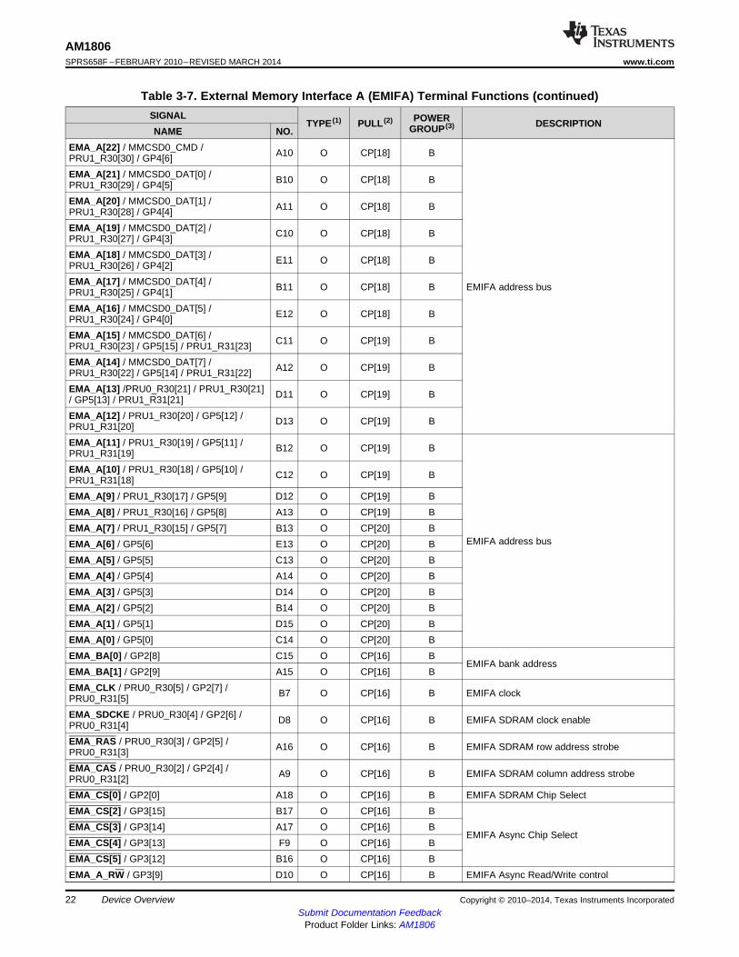
Table 3-7. External Memory Interface A (EMIFA) Terminal Functions (continued)SIGNAL POWERTYPE (1) PULL (2) DESCRIPTIONGROUP (3)NAME NO.
EMA_A[22] / MMCSD0_CMD / A10 O CP[18] BPRU1_R30[30] / GP4[6]EMA_A[21] / MMCSD0_DAT[0] / B10 O CP[18] BPRU1_R30[29] / GP4[5]EMA_A[20] / MMCSD0_DAT[1] / A11 O CP[18] BPRU1_R30[28] / GP4[4]EMA_A[19] / MMCSD0_DAT[2] / C10 O CP[18] BPRU1_R30[27] / GP4[3]EMA_A[18] / MMCSD0_DAT[3] / E11 O CP[18] BPRU1_R30[26] / GP4[2]EMA_A[17] / MMCSD0_DAT[4] / B11 O CP[18] B EMIFA address busPRU1_R30[25] / GP4[1]EMA_A[16] / MMCSD0_DAT[5] / E12 O CP[18] BPRU1_R30[24] / GP4[0]EMA_A[15] / MMCSD0_DAT[6] / C11 O CP[19] BPRU1_R30[23] / GP5[15] / PRU1_R31[23]EMA_A[14] / MMCSD0_DAT[7] / A12 O CP[19] BPRU1_R30[22] / GP5[14] / PRU1_R31[22]EMA_A[13] /PRU0_R30[21] / PRU1_R30[21] D11 O CP[19] B/ GP5[13] / PRU1_R31[21]EMA_A[12] / PRU1_R30[20] / GP5[12] / D13 O CP[19] BPRU1_R31[20]EMA_A[11] / PRU1_R30[19] / GP5[11] / B12 O CP[19] BPRU1_R31[19]EMA_A[10] / PRU1_R30[18] / GP5[10] / C12 O CP[19] BPRU1_R31[18]EMA_A[9] / PRU1_R30[17] / GP5[9] D12 O CP[19] BEMA_A[8] / PRU1_R30[16] / GP5[8] A13 O CP[19] BEMA_A[7] / PRU1_R30[15] / GP5[7] B13 O CP[20] B
EMIFA address busEMA_A[6] / GP5[6] E13 O CP[20] BEMA_A[5] / GP5[5] C13 O CP[20] BEMA_A[4] / GP5[4] A14 O CP[20] BEMA_A[3] / GP5[3] D14 O CP[20] BEMA_A[2] / GP5[2] B14 O CP[20] BEMA_A[1] / GP5[1] D15 O CP[20] BEMA_A[0] / GP5[0] C14 O CP[20] BEMA_BA[0] / GP2[8] C15 O CP[16] B
EMIFA bank addressEMA_BA[1] / GP2[9] A15 O CP[16] BEMA_CLK / PRU0_R30[5] / GP2[7] / B7 O CP[16] B EMIFA clockPRU0_R31[5]EMA_SDCKE / PRU0_R30[4] / GP2[6] / D8 O CP[16] B EMIFA SDRAM clock enablePRU0_R31[4]EMA_RAS / PRU0_R30[3] / GP2[5] / A16 O CP[16] B EMIFA SDRAM row address strobePRU0_R31[3]EMA_CAS / PRU0_R30[2] / GP2[4] / A9 O CP[16] B EMIFA SDRAM column address strobePRU0_R31[2]EMA_CS[0] / GP2[0] A18 O CP[16] B EMIFA SDRAM Chip SelectEMA_CS[2] / GP3[15] B17 O CP[16] BEMA_CS[3] / GP3[14] A17 O CP[16] B
EMIFA Async Chip SelectEMA_CS[4] / GP3[13] F9 O CP[16] BEMA_CS[5] / GP3[12] B16 O CP[16] BEMA_A_RW / GP3[9] D10 O CP[16] B EMIFA Async Read/Write control
22 Device Overview Copyright © 2010–2014, Texas Instruments IncorporatedSubmit Documentation Feedback
Product Folder Links: AM1806
AM1806www.ti.com SPRS658F –FEBRUARY 2010–REVISED MARCH 2014
Table 3-7. External Memory Interface A (EMIFA) Terminal Functions (continued)SIGNAL POWERTYPE (1) PULL (2) DESCRIPTIONGROUP (3)NAME NO.
EMA_WE / GP3[11] B9 O CP[16] B EMIFA SDRAM write enableEMIFA write enable/data mask forEMA_WEN_DQM[1] / GP2[2] A5 O CP[16] B EMA_D[15:8]
EMA_WEN_DQM[0] / GP2[3] C8 O CP[16] B EMIFA write enable/data mask for EMA_D[7:0]EMA_OE / GP3[10] B15 O CP[16] B EMIFA output enableEMA_WAIT[0] / PRU0_R30[0] / GP3[8] / B18 I CP[16] BPRU0_R31[0]
EMIFA wait input/interruptEMA_WAIT[1] / PRU0_R30[1] / GP2[1] / B19 I CP[16] BPRU0_R31[1]
Copyright © 2010–2014, Texas Instruments Incorporated Device Overview 23Submit Documentation Feedback
Product Folder Links: AM1806
AM1806SPRS658F –FEBRUARY 2010–REVISED MARCH 2014 www.ti.com
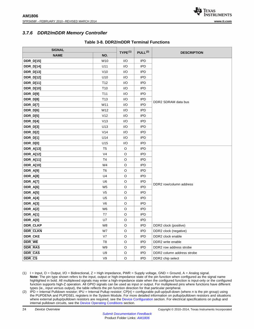
3.7.6 DDR2/mDDR Memory Controller
Table 3-8. DDR2/mDDR Terminal Functions
SIGNALTYPE (1) PULL (2) DESCRIPTION
NAME NO.DDR_D[15] W10 I/O IPDDDR_D[14] U11 I/O IPDDDR_D[13] V10 I/O IPDDDR_D[12] U10 I/O IPDDDR_D[11] T12 I/O IPDDDR_D[10] T10 I/O IPDDDR_D[9] T11 I/O IPDDDR_D[8] T13 I/O IPD
DDR2 SDRAM data busDDR_D[7] W11 I/O IPDDDR_D[6] W12 I/O IPDDDR_D[5] V12 I/O IPDDDR_D[4] V13 I/O IPDDDR_D[3] U13 I/O IPDDDR_D[2] V14 I/O IPDDDR_D[1] U14 I/O IPDDDR_D[0] U15 I/O IPDDDR_A[13] T5 O IPDDDR_A[12] V4 O IPDDDR_A[11] T4 O IPDDDR_A[10] W4 O IPDDDR_A[9] T6 O IPDDDR_A[8] U4 O IPDDDR_A[7] U6 O IPD
DDR2 row/column addressDDR_A[6] W5 O IPDDDR_A[5] V5 O IPDDDR_A[4] U5 O IPDDDR_A[3] V6 O IPDDDR_A[2] W6 O IPDDDR_A[1] T7 O IPDDDR_A[0] U7 O IPDDDR_CLKP W8 O IPD DDR2 clock (positive)DDR_CLKN W7 O IPD DDR2 clock (negative)DDR_CKE V7 O IPD DDR2 clock enableDDR_WE T8 O IPD DDR2 write enableDDR_RAS W9 O IPD DDR2 row address strobeDDR_CAS U9 O IPD DDR2 column address strobeDDR_CS V9 O IPD DDR2 chip select
(1) I = Input, O = Output, I/O = Bidirectional, Z = High impedance, PWR = Supply voltage, GND = Ground, A = Analog signal.Note: The pin type shown refers to the input, output or high-impedance state of the pin function when configured as the signal namehighlighted in bold. All multiplexed signals may enter a high-impedance state when the configured function is input-only or the configuredfunction supports high-Z operation. All GPIO signals can be used as input or output. For multiplexed pins where functions have differenttypes (ie., input versus output), the table reflects the pin function direction for that particular peripheral.
(2) IPD = Internal Pulldown resistor; IPU = Internal Pullup resistor; CP[n] = configurable pull-up/pull-down (where n is the pin group) usingthe PUPDENA and PUPDSEL registers in the System Module. For more detailed information on pullup/pulldown resistors and situationswhere external pullup/pulldown resistors are required, see the Device Configuration section. For electrical specifications on pullup andinternal pulldown circuits, see the Device Operating Conditions section.
24 Device Overview Copyright © 2010–2014, Texas Instruments IncorporatedSubmit Documentation Feedback
Product Folder Links: AM1806
AM1806www.ti.com SPRS658F –FEBRUARY 2010–REVISED MARCH 2014
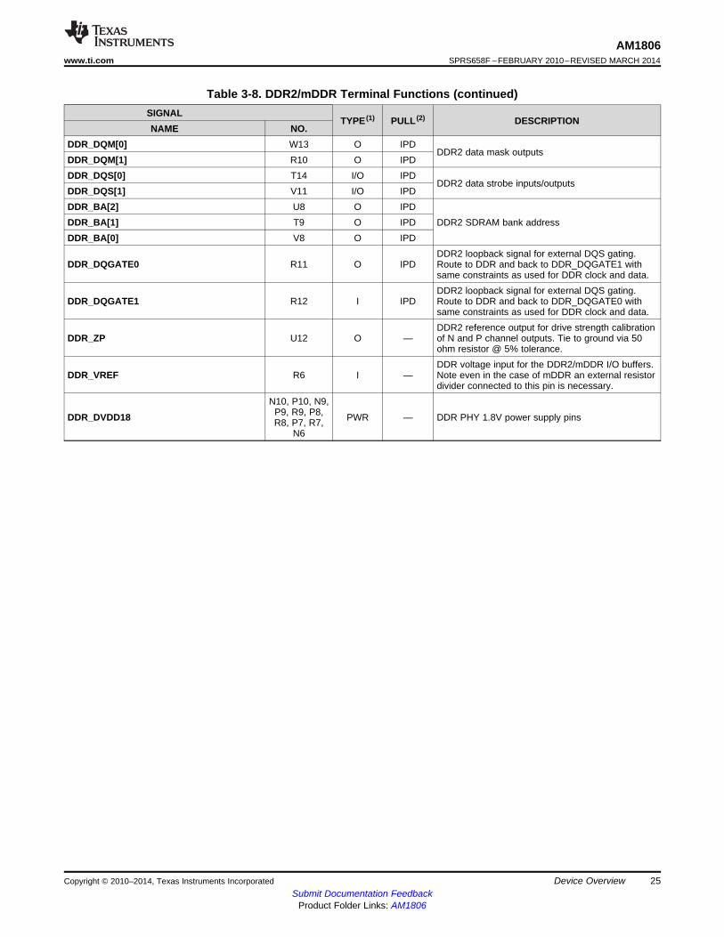
Table 3-8. DDR2/mDDR Terminal Functions (continued)SIGNAL
TYPE (1) PULL (2) DESCRIPTIONNAME NO.
DDR_DQM[0] W13 O IPDDDR2 data mask outputs
DDR_DQM[1] R10 O IPDDDR_DQS[0] T14 I/O IPD
DDR2 data strobe inputs/outputsDDR_DQS[1] V11 I/O IPDDDR_BA[2] U8 O IPDDDR_BA[1] T9 O IPD DDR2 SDRAM bank addressDDR_BA[0] V8 O IPD
DDR2 loopback signal for external DQS gating.DDR_DQGATE0 R11 O IPD Route to DDR and back to DDR_DQGATE1 with
same constraints as used for DDR clock and data.DDR2 loopback signal for external DQS gating.
DDR_DQGATE1 R12 I IPD Route to DDR and back to DDR_DQGATE0 withsame constraints as used for DDR clock and data.DDR2 reference output for drive strength calibration
DDR_ZP U12 O — of N and P channel outputs. Tie to ground via 50ohm resistor @ 5% tolerance.DDR voltage input for the DDR2/mDDR I/O buffers.
DDR_VREF R6 I — Note even in the case of mDDR an external resistordivider connected to this pin is necessary.
N10, P10, N9,P9, R9, P8,DDR_DVDD18 PWR — DDR PHY 1.8V power supply pinsR8, P7, R7,
N6
Copyright © 2010–2014, Texas Instruments Incorporated Device Overview 25Submit Documentation Feedback
Product Folder Links: AM1806
AM1806SPRS658F –FEBRUARY 2010–REVISED MARCH 2014 www.ti.com
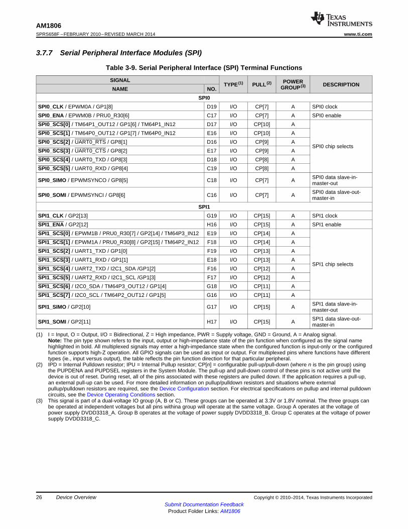
3.7.7 Serial Peripheral Interface Modules (SPI)
Table 3-9. Serial Peripheral Interface (SPI) Terminal Functions
SIGNAL POWERTYPE (1) PULL (2) DESCRIPTIONGROUP (3)NAME NO.SPI0
SPI0_CLK / EPWM0A / GP1[8] D19 I/O CP[7] A SPI0 clockSPI0_ENA / EPWM0B / PRU0_R30[6] C17 I/O CP[7] A SPI0 enableSPI0_SCS[0] / TM64P1_OUT12 / GP1[6] / TM64P1_IN12 D17 I/O CP[10] ASPI0_SCS[1] / TM64P0_OUT12 / GP1[7] / TM64P0_IN12 E16 I/O CP[10] ASPI0_SCS[2] / UART0_RTS / GP8[1] D16 I/O CP[9] A
SPI0 chip selectsSPI0_SCS[3] / UART0_CTS / GP8[2] E17 I/O CP[9] ASPI0_SCS[4] / UART0_TXD / GP8[3] D18 I/O CP[8] ASPI0_SCS[5] / UART0_RXD / GP8[4] C19 I/O CP[8] A
SPI0 data slave-in-SPI0_SIMO / EPWMSYNCO / GP8[5] C18 I/O CP[7] A master-outSPI0 data slave-out-SPI0_SOMI / EPWMSYNCI / GP8[6] C16 I/O CP[7] A master-in
SPI1SPI1_CLK / GP2[13] G19 I/O CP[15] A SPI1 clockSPI1_ENA / GP2[12] H16 I/O CP[15] A SPI1 enableSPI1_SCS[0] / EPWM1B / PRU0_R30[7] / GP2[14] / TM64P3_IN12 E19 I/O CP[14] ASPI1_SCS[1] / EPWM1A / PRU0_R30[8] / GP2[15] / TM64P2_IN12 F18 I/O CP[14] ASPI1_SCS[2] / UART1_TXD / GP1[0] F19 I/O CP[13] ASPI1_SCS[3] / UART1_RXD / GP1[1] E18 I/O CP[13] A
SPI1 chip selectsSPI1_SCS[4] / UART2_TXD / I2C1_SDA /GP1[2] F16 I/O CP[12] ASPI1_SCS[5] / UART2_RXD / I2C1_SCL /GP1[3] F17 I/O CP[12] ASPI1_SCS[6] / I2C0_SDA / TM64P3_OUT12 / GP1[4] G18 I/O CP[11] ASPI1_SCS[7] / I2C0_SCL / TM64P2_OUT12 / GP1[5] G16 I/O CP[11] A
SPI1 data slave-in-SPI1_SIMO / GP2[10] G17 I/O CP[15] A master-outSPI1 data slave-out-SPI1_SOMI / GP2[11] H17 I/O CP[15] A master-in
(1) I = Input, O = Output, I/O = Bidirectional, Z = High impedance, PWR = Supply voltage, GND = Ground, A = Analog signal.Note: The pin type shown refers to the input, output or high-impedance state of the pin function when configured as the signal namehighlighted in bold. All multiplexed signals may enter a high-impedance state when the configured function is input-only or the configuredfunction supports high-Z operation. All GPIO signals can be used as input or output. For multiplexed pins where functions have differenttypes (ie., input versus output), the table reflects the pin function direction for that particular peripheral.
(2) IPD = Internal Pulldown resistor; IPU = Internal Pullup resistor; CP[n] = configurable pull-up/pull-down (where n is the pin group) usingthe PUPDENA and PUPDSEL registers in the System Module. The pull-up and pull-down control of these pins is not active until thedevice is out of reset. During reset, all of the pins associated with these registers are pulled down. If the application requires a pull-up,an external pull-up can be used. For more detailed information on pullup/pulldown resistors and situations where externalpullup/pulldown resistors are required, see the Device Configuration section. For electrical specifications on pullup and internal pulldowncircuits, see the Device Operating Conditions section.
(3) This signal is part of a dual-voltage IO group (A, B or C). These groups can be operated at 3.3V or 1.8V nominal. The three groups canbe operated at independent voltages but all pins withina group will operate at the same voltage. Group A operates at the voltage ofpower supply DVDD3318_A. Group B operates at the voltage of power supply DVDD3318_B. Group C operates at the voltage of powersupply DVDD3318_C.
26 Device Overview Copyright © 2010–2014, Texas Instruments IncorporatedSubmit Documentation Feedback
Product Folder Links: AM1806
AM1806www.ti.com SPRS658F –FEBRUARY 2010–REVISED MARCH 2014
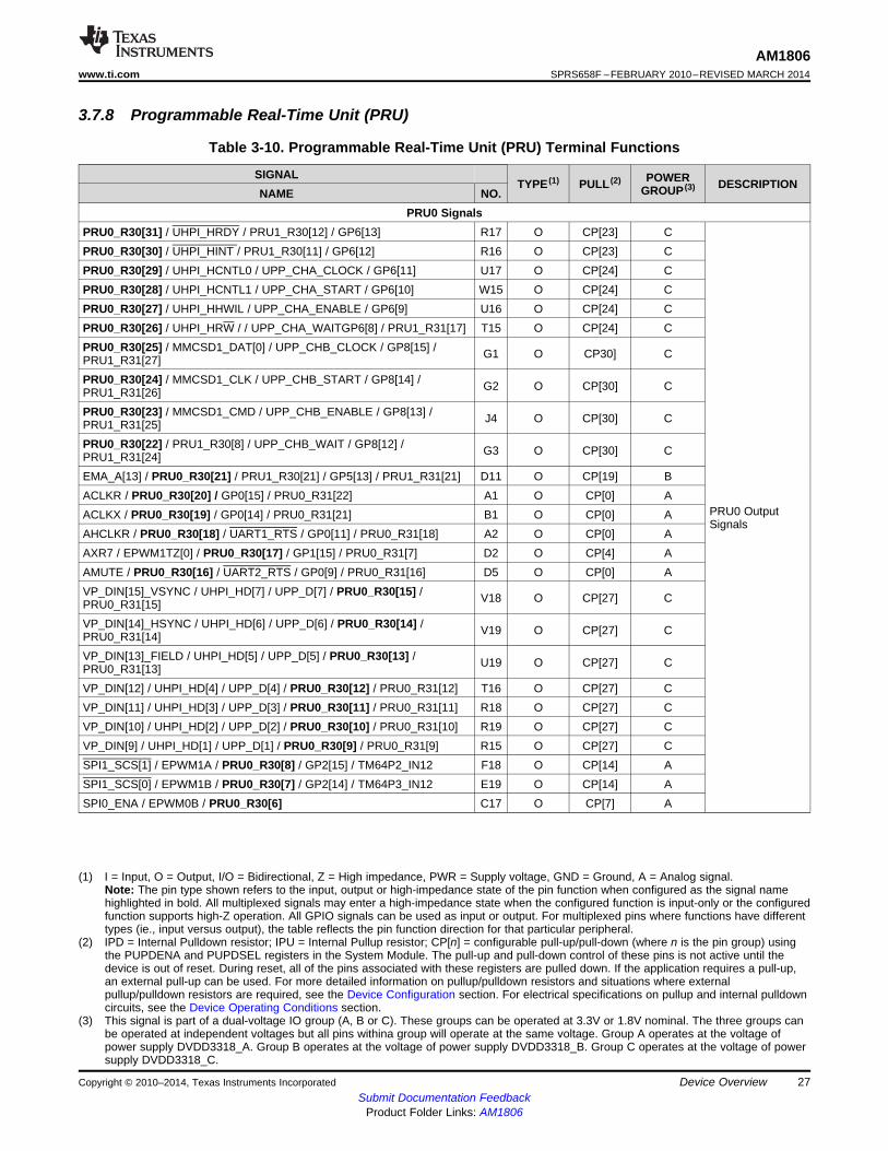
3.7.8 Programmable Real-Time Unit (PRU)
Table 3-10. Programmable Real-Time Unit (PRU) Terminal Functions
SIGNAL POWERTYPE (1) PULL (2) DESCRIPTIONGROUP (3)NAME NO.PRU0 Signals
PRU0_R30[31] / UHPI_HRDY / PRU1_R30[12] / GP6[13] R17 O CP[23] CPRU0_R30[30] / UHPI_HINT / PRU1_R30[11] / GP6[12] R16 O CP[23] CPRU0_R30[29] / UHPI_HCNTL0 / UPP_CHA_CLOCK / GP6[11] U17 O CP[24] CPRU0_R30[28] / UHPI_HCNTL1 / UPP_CHA_START / GP6[10] W15 O CP[24] CPRU0_R30[27] / UHPI_HHWIL / UPP_CHA_ENABLE / GP6[9] U16 O CP[24] CPRU0_R30[26] / UHPI_HRW / / UPP_CHA_WAITGP6[8] / PRU1_R31[17] T15 O CP[24] CPRU0_R30[25] / MMCSD1_DAT[0] / UPP_CHB_CLOCK / GP8[15] / G1 O CP30] CPRU1_R31[27]PRU0_R30[24] / MMCSD1_CLK / UPP_CHB_START / GP8[14] / G2 O CP[30] CPRU1_R31[26]PRU0_R30[23] / MMCSD1_CMD / UPP_CHB_ENABLE / GP8[13] / J4 O CP[30] CPRU1_R31[25]PRU0_R30[22] / PRU1_R30[8] / UPP_CHB_WAIT / GP8[12] / G3 O CP[30] CPRU1_R31[24]EMA_A[13] / PRU0_R30[21] / PRU1_R30[21] / GP5[13] / PRU1_R31[21] D11 O CP[19] BACLKR / PRU0_R30[20] / GP0[15] / PRU0_R31[22] A1 O CP[0] A
PRU0 OutputACLKX / PRU0_R30[19] / GP0[14] / PRU0_R31[21] B1 O CP[0] ASignals
AHCLKR / PRU0_R30[18] / UART1_RTS / GP0[11] / PRU0_R31[18] A2 O CP[0] AAXR7 / EPWM1TZ[0] / PRU0_R30[17] / GP1[15] / PRU0_R31[7] D2 O CP[4] AAMUTE / PRU0_R30[16] / UART2_RTS / GP0[9] / PRU0_R31[16] D5 O CP[0] AVP_DIN[15]_VSYNC / UHPI_HD[7] / UPP_D[7] / PRU0_R30[15] / V18 O CP[27] CPRU0_R31[15]VP_DIN[14]_HSYNC / UHPI_HD[6] / UPP_D[6] / PRU0_R30[14] / V19 O CP[27] CPRU0_R31[14]VP_DIN[13]_FIELD / UHPI_HD[5] / UPP_D[5] / PRU0_R30[13] / U19 O CP[27] CPRU0_R31[13]VP_DIN[12] / UHPI_HD[4] / UPP_D[4] / PRU0_R30[12] / PRU0_R31[12] T16 O CP[27] CVP_DIN[11] / UHPI_HD[3] / UPP_D[3] / PRU0_R30[11] / PRU0_R31[11] R18 O CP[27] CVP_DIN[10] / UHPI_HD[2] / UPP_D[2] / PRU0_R30[10] / PRU0_R31[10] R19 O CP[27] CVP_DIN[9] / UHPI_HD[1] / UPP_D[1] / PRU0_R30[9] / PRU0_R31[9] R15 O CP[27] CSPI1_SCS[1] / EPWM1A / PRU0_R30[8] / GP2[15] / TM64P2_IN12 F18 O CP[14] ASPI1_SCS[0] / EPWM1B / PRU0_R30[7] / GP2[14] / TM64P3_IN12 E19 O CP[14] ASPI0_ENA / EPWM0B / PRU0_R30[6] C17 O CP[7] A
(1) I = Input, O = Output, I/O = Bidirectional, Z = High impedance, PWR = Supply voltage, GND = Ground, A = Analog signal.Note: The pin type shown refers to the input, output or high-impedance state of the pin function when configured as the signal namehighlighted in bold. All multiplexed signals may enter a high-impedance state when the configured function is input-only or the configuredfunction supports high-Z operation. All GPIO signals can be used as input or output. For multiplexed pins where functions have differenttypes (ie., input versus output), the table reflects the pin function direction for that particular peripheral.
(2) IPD = Internal Pulldown resistor; IPU = Internal Pullup resistor; CP[n] = configurable pull-up/pull-down (where n is the pin group) usingthe PUPDENA and PUPDSEL registers in the System Module. The pull-up and pull-down control of these pins is not active until thedevice is out of reset. During reset, all of the pins associated with these registers are pulled down. If the application requires a pull-up,an external pull-up can be used. For more detailed information on pullup/pulldown resistors and situations where externalpullup/pulldown resistors are required, see the Device Configuration section. For electrical specifications on pullup and internal pulldowncircuits, see the Device Operating Conditions section.
(3) This signal is part of a dual-voltage IO group (A, B or C). These groups can be operated at 3.3V or 1.8V nominal. The three groups canbe operated at independent voltages but all pins withina group will operate at the same voltage. Group A operates at the voltage ofpower supply DVDD3318_A. Group B operates at the voltage of power supply DVDD3318_B. Group C operates at the voltage of powersupply DVDD3318_C.
Copyright © 2010–2014, Texas Instruments Incorporated Device Overview 27Submit Documentation Feedback
Product Folder Links: AM1806
AM1806SPRS658F –FEBRUARY 2010–REVISED MARCH 2014 www.ti.com
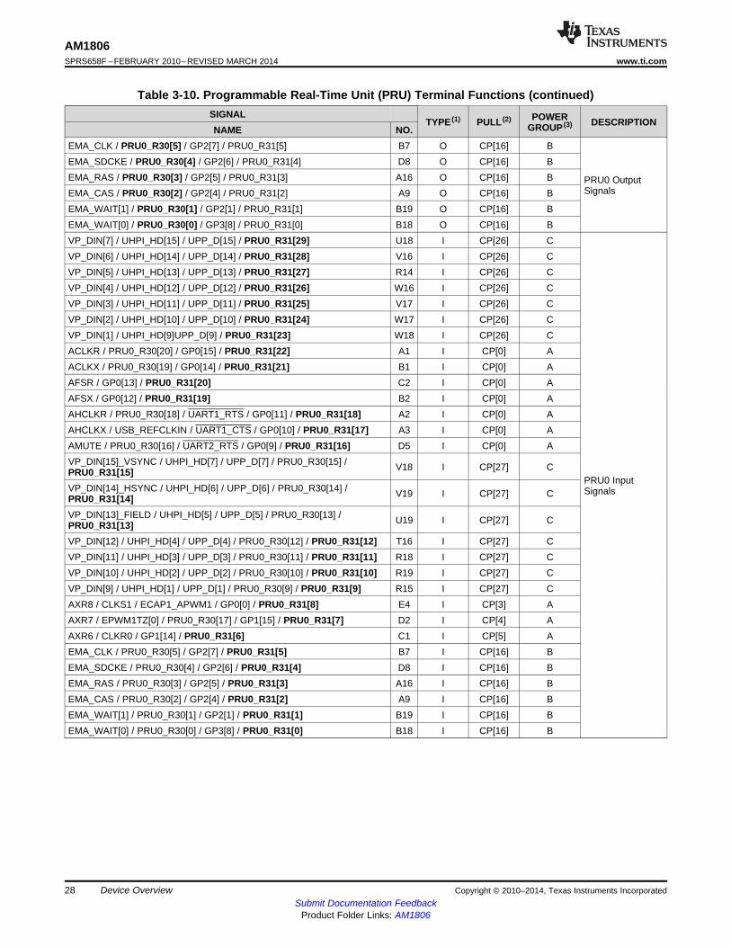
Table 3-10. Programmable Real-Time Unit (PRU) Terminal Functions (continued)SIGNAL POWERTYPE (1) PULL (2) DESCRIPTIONGROUP (3)NAME NO.
EMA_CLK / PRU0_R30[5] / GP2[7] / PRU0_R31[5] B7 O CP[16] BEMA_SDCKE / PRU0_R30[4] / GP2[6] / PRU0_R31[4] D8 O CP[16] BEMA_RAS / PRU0_R30[3] / GP2[5] / PRU0_R31[3] A16 O CP[16] B PRU0 Output
SignalsEMA_CAS / PRU0_R30[2] / GP2[4] / PRU0_R31[2] A9 O CP[16] BEMA_WAIT[1] / PRU0_R30[1] / GP2[1] / PRU0_R31[1] B19 O CP[16] BEMA_WAIT[0] / PRU0_R30[0] / GP3[8] / PRU0_R31[0] B18 O CP[16] BVP_DIN[7] / UHPI_HD[15] / UPP_D[15] / PRU0_R31[29] U18 I CP[26] CVP_DIN[6] / UHPI_HD[14] / UPP_D[14] / PRU0_R31[28] V16 I CP[26] CVP_DIN[5] / UHPI_HD[13] / UPP_D[13] / PRU0_R31[27] R14 I CP[26] CVP_DIN[4] / UHPI_HD[12] / UPP_D[12] / PRU0_R31[26] W16 I CP[26] CVP_DIN[3] / UHPI_HD[11] / UPP_D[11] / PRU0_R31[25] V17 I CP[26] CVP_DIN[2] / UHPI_HD[10] / UPP_D[10] / PRU0_R31[24] W17 I CP[26] CVP_DIN[1] / UHPI_HD[9]UPP_D[9] / PRU0_R31[23] W18 I CP[26] CACLKR / PRU0_R30[20] / GP0[15] / PRU0_R31[22] A1 I CP[0] AACLKX / PRU0_R30[19] / GP0[14] / PRU0_R31[21] B1 I CP[0] AAFSR / GP0[13] / PRU0_R31[20] C2 I CP[0] AAFSX / GP0[12] / PRU0_R31[19] B2 I CP[0] AAHCLKR / PRU0_R30[18] / UART1_RTS / GP0[11] / PRU0_R31[18] A2 I CP[0] AAHCLKX / USB_REFCLKIN / UART1_CTS / GP0[10] / PRU0_R31[17] A3 I CP[0] AAMUTE / PRU0_R30[16] / UART2_RTS / GP0[9] / PRU0_R31[16] D5 I CP[0] AVP_DIN[15]_VSYNC / UHPI_HD[7] / UPP_D[7] / PRU0_R30[15] / V18 I CP[27] CPRU0_R31[15]
PRU0 InputVP_DIN[14]_HSYNC / UHPI_HD[6] / UPP_D[6] / PRU0_R30[14] / SignalsV19 I CP[27] CPRU0_R31[14]VP_DIN[13]_FIELD / UHPI_HD[5] / UPP_D[5] / PRU0_R30[13] / U19 I CP[27] CPRU0_R31[13]VP_DIN[12] / UHPI_HD[4] / UPP_D[4] / PRU0_R30[12] / PRU0_R31[12] T16 I CP[27] CVP_DIN[11] / UHPI_HD[3] / UPP_D[3] / PRU0_R30[11] / PRU0_R31[11] R18 I CP[27] CVP_DIN[10] / UHPI_HD[2] / UPP_D[2] / PRU0_R30[10] / PRU0_R31[10] R19 I CP[27] CVP_DIN[9] / UHPI_HD[1] / UPP_D[1] / PRU0_R30[9] / PRU0_R31[9] R15 I CP[27] CAXR8 / CLKS1 / ECAP1_APWM1 / GP0[0] / PRU0_R31[8] E4 I CP[3] AAXR7 / EPWM1TZ[0] / PRU0_R30[17] / GP1[15] / PRU0_R31[7] D2 I CP[4] AAXR6 / CLKR0 / GP1[14] / PRU0_R31[6] C1 I CP[5] AEMA_CLK / PRU0_R30[5] / GP2[7] / PRU0_R31[5] B7 I CP[16] BEMA_SDCKE / PRU0_R30[4] / GP2[6] / PRU0_R31[4] D8 I CP[16] BEMA_RAS / PRU0_R30[3] / GP2[5] / PRU0_R31[3] A16 I CP[16] BEMA_CAS / PRU0_R30[2] / GP2[4] / PRU0_R31[2] A9 I CP[16] BEMA_WAIT[1] / PRU0_R30[1] / GP2[1] / PRU0_R31[1] B19 I CP[16] BEMA_WAIT[0] / PRU0_R30[0] / GP3[8] / PRU0_R31[0] B18 I CP[16] B
28 Device Overview Copyright © 2010–2014, Texas Instruments IncorporatedSubmit Documentation Feedback
Product Folder Links: AM1806
AM1806www.ti.com SPRS658F –FEBRUARY 2010–REVISED MARCH 2014
Table 3-10. Programmable Real-Time Unit (PRU) Terminal Functions (continued)SIGNAL POWERTYPE (1) PULL (2) DESCRIPTIONGROUP (3)NAME NO.
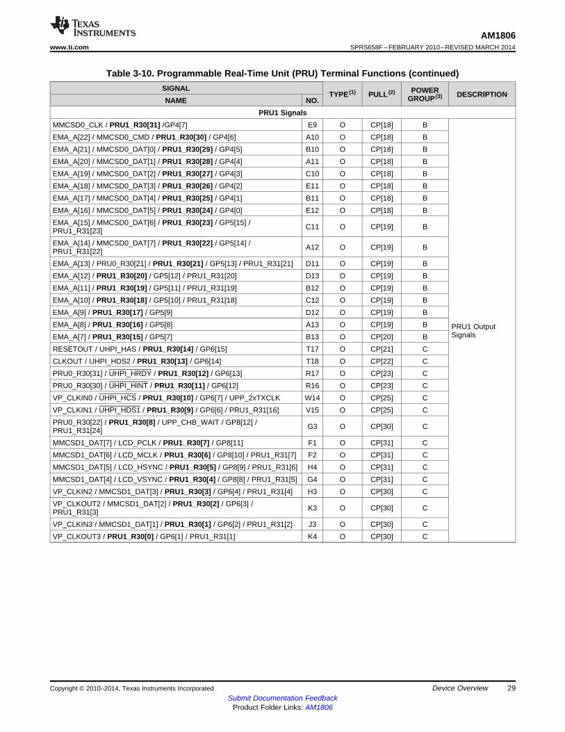
PRU1 SignalsMMCSD0_CLK / PRU1_R30[31] /GP4[7] E9 O CP[18] BEMA_A[22] / MMCSD0_CMD / PRU1_R30[30] / GP4[6] A10 O CP[18] BEMA_A[21] / MMCSD0_DAT[0] / PRU1_R30[29] / GP4[5] B10 O CP[18] BEMA_A[20] / MMCSD0_DAT[1] / PRU1_R30[28] / GP4[4] A11 O CP[18] BEMA_A[19] / MMCSD0_DAT[2] / PRU1_R30[27] / GP4[3] C10 O CP[18] BEMA_A[18] / MMCSD0_DAT[3] / PRU1_R30[26] / GP4[2] E11 O CP[18] BEMA_A[17] / MMCSD0_DAT[4] / PRU1_R30[25] / GP4[1] B11 O CP[18] BEMA_A[16] / MMCSD0_DAT[5] / PRU1_R30[24] / GP4[0] E12 O CP[18] BEMA_A[15] / MMCSD0_DAT[6] / PRU1_R30[23] / GP5[15] / C11 O CP[19] BPRU1_R31[23]EMA_A[14] / MMCSD0_DAT[7] / PRU1_R30[22] / GP5[14] / A12 O CP[19] BPRU1_R31[22]EMA_A[13] / PRU0_R30[21] / PRU1_R30[21] / GP5[13] / PRU1_R31[21] D11 O CP[19] BEMA_A[12] / PRU1_R30[20] / GP5[12] / PRU1_R31[20] D13 O CP[19] BEMA_A[11] / PRU1_R30[19] / GP5[11] / PRU1_R31[19] B12 O CP[19] BEMA_A[10] / PRU1_R30[18] / GP5[10] / PRU1_R31[18] C12 O CP[19] BEMA_A[9] / PRU1_R30[17] / GP5[9] D12 O CP[19] BEMA_A[8] / PRU1_R30[16] / GP5[8] A13 O CP[19] B PRU1 Output
SignalsEMA_A[7] / PRU1_R30[15] / GP5[7] B13 O CP[20] BRESETOUT / UHPI_HAS / PRU1_R30[14] / GP6[15] T17 O CP[21] CCLKOUT / UHPI_HDS2 / PRU1_R30[13] / GP6[14] T18 O CP[22] CPRU0_R30[31] / UHPI_HRDY / PRU1_R30[12] / GP6[13] R17 O CP[23] CPRU0_R30[30] / UHPI_HINT / PRU1_R30[11] / GP6[12] R16 O CP[23] CVP_CLKIN0 / UHPI_HCS / PRU1_R30[10] / GP6[7] / UPP_2xTXCLK W14 O CP[25] CVP_CLKIN1 / UHPI_HDS1 / PRU1_R30[9] / GP6[6] / PRU1_R31[16] V15 O CP[25] CPRU0_R30[22] / PRU1_R30[8] / UPP_CHB_WAIT / GP8[12] / G3 O CP[30] CPRU1_R31[24]MMCSD1_DAT[7] / LCD_PCLK / PRU1_R30[7] / GP8[11] F1 O CP[31] CMMCSD1_DAT[6] / LCD_MCLK / PRU1_R30[6] / GP8[10] / PRU1_R31[7] F2 O CP[31] CMMCSD1_DAT[5] / LCD_HSYNC / PRU1_R30[5] / GP8[9] / PRU1_R31[6] H4 O CP[31] CMMCSD1_DAT[4] / LCD_VSYNC / PRU1_R30[4] / GP8[8] / PRU1_R31[5] G4 O CP[31] CVP_CLKIN2 / MMCSD1_DAT[3] / PRU1_R30[3] / GP6[4] / PRU1_R31[4] H3 O CP[30] CVP_CLKOUT2 / MMCSD1_DAT[2] / PRU1_R30[2] / GP6[3] / K3 O CP[30] CPRU1_R31[3]VP_CLKIN3 / MMCSD1_DAT[1] / PRU1_R30[1] / GP6[2] / PRU1_R31[2] J3 O CP[30] CVP_CLKOUT3 / PRU1_R30[0] / GP6[1] / PRU1_R31[1] K4 O CP[30] C
Copyright © 2010–2014, Texas Instruments Incorporated Device Overview 29Submit Documentation Feedback
Product Folder Links: AM1806
AM1806SPRS658F –FEBRUARY 2010–REVISED MARCH 2014 www.ti.com
Table 3-10. Programmable Real-Time Unit (PRU) Terminal Functions (continued)SIGNAL POWERTYPE (1) PULL (2) DESCRIPTIONGROUP (3)NAME NO.
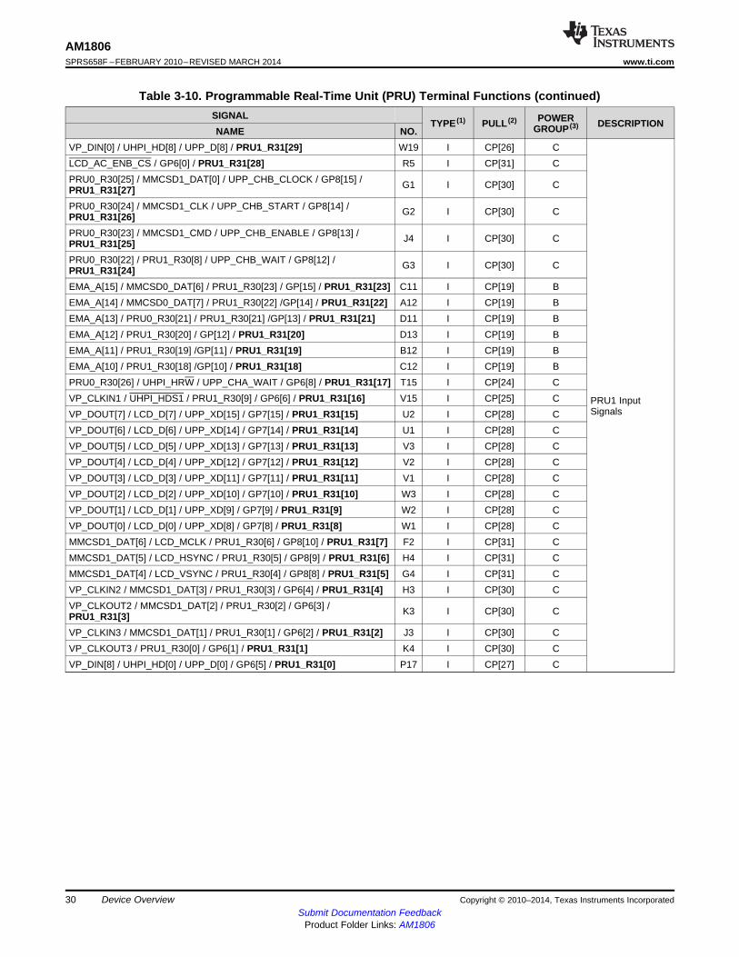
VP_DIN[0] / UHPI_HD[8] / UPP_D[8] / PRU1_R31[29] W19 I CP[26] CLCD_AC_ENB_CS / GP6[0] / PRU1_R31[28] R5 I CP[31] CPRU0_R30[25] / MMCSD1_DAT[0] / UPP_CHB_CLOCK / GP8[15] / G1 I CP[30] CPRU1_R31[27]PRU0_R30[24] / MMCSD1_CLK / UPP_CHB_START / GP8[14] / G2 I CP[30] CPRU1_R31[26]PRU0_R30[23] / MMCSD1_CMD / UPP_CHB_ENABLE / GP8[13] / J4 I CP[30] CPRU1_R31[25]PRU0_R30[22] / PRU1_R30[8] / UPP_CHB_WAIT / GP8[12] / G3 I CP[30] CPRU1_R31[24]EMA_A[15] / MMCSD0_DAT[6] / PRU1_R30[23] / GP[15] / PRU1_R31[23] C11 I CP[19] BEMA_A[14] / MMCSD0_DAT[7] / PRU1_R30[22] /GP[14] / PRU1_R31[22] A12 I CP[19] BEMA_A[13] / PRU0_R30[21] / PRU1_R30[21] /GP[13] / PRU1_R31[21] D11 I CP[19] BEMA_A[12] / PRU1_R30[20] / GP[12] / PRU1_R31[20] D13 I CP[19] BEMA_A[11] / PRU1_R30[19] /GP[11] / PRU1_R31[19] B12 I CP[19] BEMA_A[10] / PRU1_R30[18] /GP[10] / PRU1_R31[18] C12 I CP[19] BPRU0_R30[26] / UHPI_HRW / UPP_CHA_WAIT / GP6[8] / PRU1_R31[17] T15 I CP[24] CVP_CLKIN1 / UHPI_HDS1 / PRU1_R30[9] / GP6[6] / PRU1_R31[16] V15 I CP[25] C PRU1 Input
SignalsVP_DOUT[7] / LCD_D[7] / UPP_XD[15] / GP7[15] / PRU1_R31[15] U2 I CP[28] CVP_DOUT[6] / LCD_D[6] / UPP_XD[14] / GP7[14] / PRU1_R31[14] U1 I CP[28] CVP_DOUT[5] / LCD_D[5] / UPP_XD[13] / GP7[13] / PRU1_R31[13] V3 I CP[28] CVP_DOUT[4] / LCD_D[4] / UPP_XD[12] / GP7[12] / PRU1_R31[12] V2 I CP[28] CVP_DOUT[3] / LCD_D[3] / UPP_XD[11] / GP7[11] / PRU1_R31[11] V1 I CP[28] CVP_DOUT[2] / LCD_D[2] / UPP_XD[10] / GP7[10] / PRU1_R31[10] W3 I CP[28] CVP_DOUT[1] / LCD_D[1] / UPP_XD[9] / GP7[9] / PRU1_R31[9] W2 I CP[28] CVP_DOUT[0] / LCD_D[0] / UPP_XD[8] / GP7[8] / PRU1_R31[8] W1 I CP[28] CMMCSD1_DAT[6] / LCD_MCLK / PRU1_R30[6] / GP8[10] / PRU1_R31[7] F2 I CP[31] CMMCSD1_DAT[5] / LCD_HSYNC / PRU1_R30[5] / GP8[9] / PRU1_R31[6] H4 I CP[31] CMMCSD1_DAT[4] / LCD_VSYNC / PRU1_R30[4] / GP8[8] / PRU1_R31[5] G4 I CP[31] CVP_CLKIN2 / MMCSD1_DAT[3] / PRU1_R30[3] / GP6[4] / PRU1_R31[4] H3 I CP[30] CVP_CLKOUT2 / MMCSD1_DAT[2] / PRU1_R30[2] / GP6[3] / K3 I CP[30] CPRU1_R31[3]VP_CLKIN3 / MMCSD1_DAT[1] / PRU1_R30[1] / GP6[2] / PRU1_R31[2] J3 I CP[30] CVP_CLKOUT3 / PRU1_R30[0] / GP6[1] / PRU1_R31[1] K4 I CP[30] CVP_DIN[8] / UHPI_HD[0] / UPP_D[0] / GP6[5] / PRU1_R31[0] P17 I CP[27] C
30 Device Overview Copyright © 2010–2014, Texas Instruments IncorporatedSubmit Documentation Feedback
Product Folder Links: AM1806
AM1806www.ti.com SPRS658F –FEBRUARY 2010–REVISED MARCH 2014
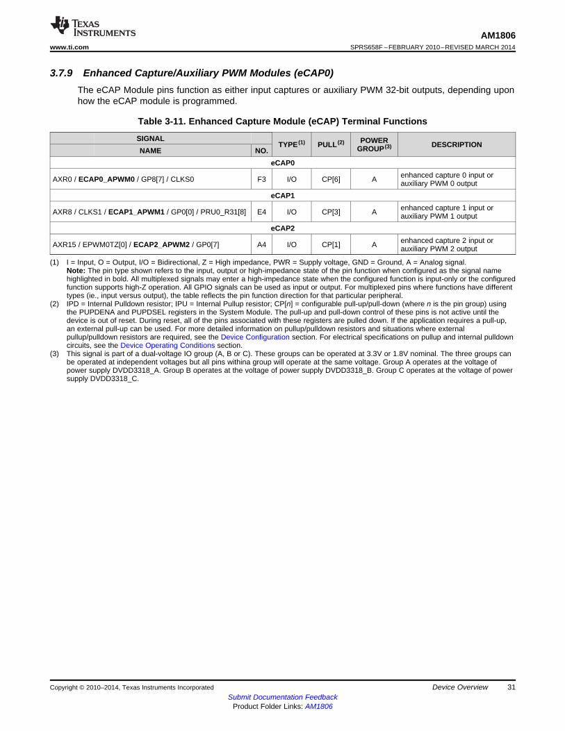
3.7.9 Enhanced Capture/Auxiliary PWM Modules (eCAP0)The eCAP Module pins function as either input captures or auxiliary PWM 32-bit outputs, depending uponhow the eCAP module is programmed.
Table 3-11. Enhanced Capture Module (eCAP) Terminal Functions
SIGNAL POWERTYPE (1) PULL (2) DESCRIPTIONGROUP (3)NAME NO.eCAP0
enhanced capture 0 input orAXR0 / ECAP0_APWM0 / GP8[7] / CLKS0 F3 I/O CP[6] A auxiliary PWM 0 outputeCAP1
enhanced capture 1 input orAXR8 / CLKS1 / ECAP1_APWM1 / GP0[0] / PRU0_R31[8] E4 I/O CP[3] A auxiliary PWM 1 outputeCAP2
enhanced capture 2 input orAXR15 / EPWM0TZ[0] / ECAP2_APWM2 / GP0[7] A4 I/O CP[1] A auxiliary PWM 2 output
(1) I = Input, O = Output, I/O = Bidirectional, Z = High impedance, PWR = Supply voltage, GND = Ground, A = Analog signal.Note: The pin type shown refers to the input, output or high-impedance state of the pin function when configured as the signal namehighlighted in bold. All multiplexed signals may enter a high-impedance state when the configured function is input-only or the configuredfunction supports high-Z operation. All GPIO signals can be used as input or output. For multiplexed pins where functions have differenttypes (ie., input versus output), the table reflects the pin function direction for that particular peripheral.
(2) IPD = Internal Pulldown resistor; IPU = Internal Pullup resistor; CP[n] = configurable pull-up/pull-down (where n is the pin group) usingthe PUPDENA and PUPDSEL registers in the System Module. The pull-up and pull-down control of these pins is not active until thedevice is out of reset. During reset, all of the pins associated with these registers are pulled down. If the application requires a pull-up,an external pull-up can be used. For more detailed information on pullup/pulldown resistors and situations where externalpullup/pulldown resistors are required, see the Device Configuration section. For electrical specifications on pullup and internal pulldowncircuits, see the Device Operating Conditions section.
(3) This signal is part of a dual-voltage IO group (A, B or C). These groups can be operated at 3.3V or 1.8V nominal. The three groups canbe operated at independent voltages but all pins withina group will operate at the same voltage. Group A operates at the voltage ofpower supply DVDD3318_A. Group B operates at the voltage of power supply DVDD3318_B. Group C operates at the voltage of powersupply DVDD3318_C.
Copyright © 2010–2014, Texas Instruments Incorporated Device Overview 31Submit Documentation Feedback
Product Folder Links: AM1806
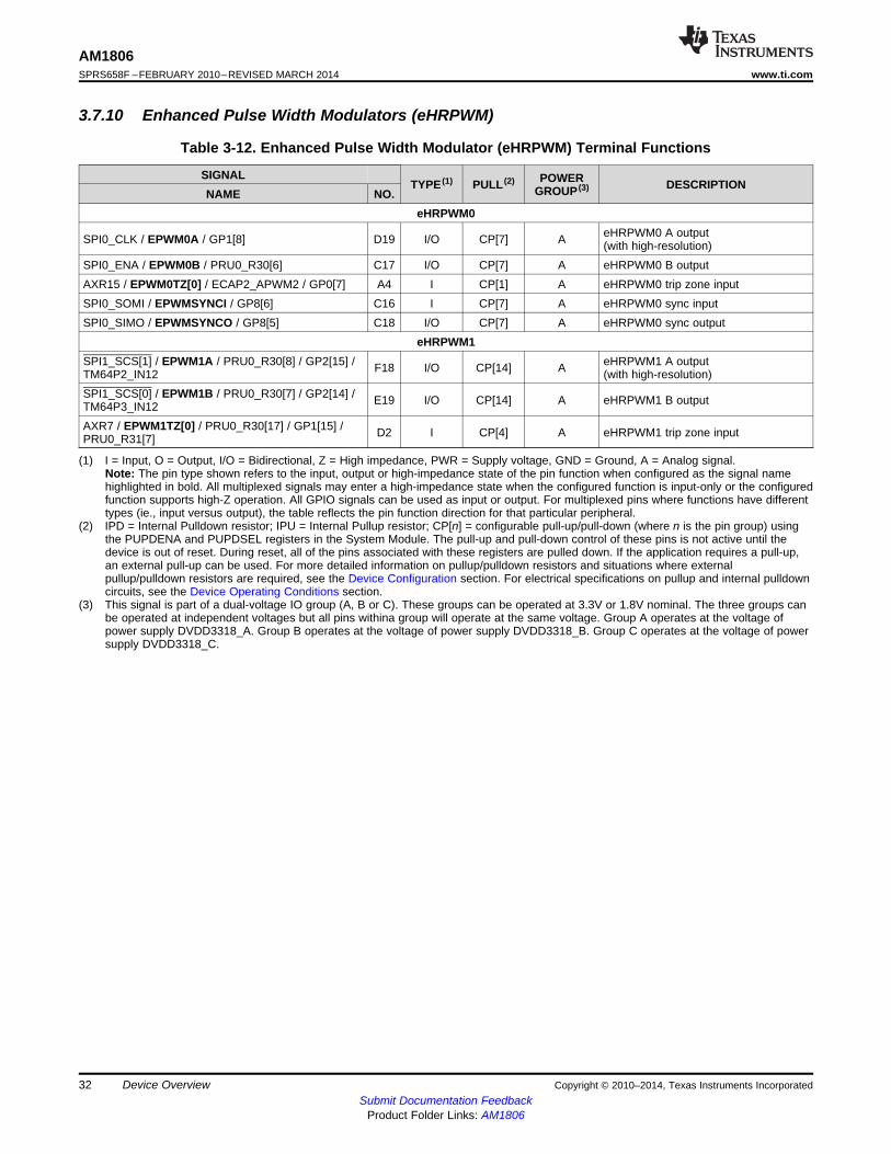
AM1806SPRS658F –FEBRUARY 2010–REVISED MARCH 2014 www.ti.com
3.7.10 Enhanced Pulse Width Modulators (eHRPWM)
Table 3-12. Enhanced Pulse Width Modulator (eHRPWM) Terminal Functions
SIGNAL POWERTYPE (1) PULL (2) DESCRIPTIONGROUP (3)NAME NO.eHRPWM0
eHRPWM0 A outputSPI0_CLK / EPWM0A / GP1[8] D19 I/O CP[7] A (with high-resolution)SPI0_ENA / EPWM0B / PRU0_R30[6] C17 I/O CP[7] A eHRPWM0 B outputAXR15 / EPWM0TZ[0] / ECAP2_APWM2 / GP0[7] A4 I CP[1] A eHRPWM0 trip zone inputSPI0_SOMI / EPWMSYNCI / GP8[6] C16 I CP[7] A eHRPWM0 sync inputSPI0_SIMO / EPWMSYNCO / GP8[5] C18 I/O CP[7] A eHRPWM0 sync output
eHRPWM1SPI1_SCS[1] / EPWM1A / PRU0_R30[8] / GP2[15] / eHRPWM1 A outputF18 I/O CP[14] ATM64P2_IN12 (with high-resolution)SPI1_SCS[0] / EPWM1B / PRU0_R30[7] / GP2[14] / E19 I/O CP[14] A eHRPWM1 B outputTM64P3_IN12AXR7 / EPWM1TZ[0] / PRU0_R30[17] / GP1[15] / D2 I CP[4] A eHRPWM1 trip zone inputPRU0_R31[7]
(1) I = Input, O = Output, I/O = Bidirectional, Z = High impedance, PWR = Supply voltage, GND = Ground, A = Analog signal.Note: The pin type shown refers to the input, output or high-impedance state of the pin function when configured as the signal namehighlighted in bold. All multiplexed signals may enter a high-impedance state when the configured function is input-only or the configuredfunction supports high-Z operation. All GPIO signals can be used as input or output. For multiplexed pins where functions have differenttypes (ie., input versus output), the table reflects the pin function direction for that particular peripheral.
(2) IPD = Internal Pulldown resistor; IPU = Internal Pullup resistor; CP[n] = configurable pull-up/pull-down (where n is the pin group) usingthe PUPDENA and PUPDSEL registers in the System Module. The pull-up and pull-down control of these pins is not active until thedevice is out of reset. During reset, all of the pins associated with these registers are pulled down. If the application requires a pull-up,an external pull-up can be used. For more detailed information on pullup/pulldown resistors and situations where externalpullup/pulldown resistors are required, see the Device Configuration section. For electrical specifications on pullup and internal pulldowncircuits, see the Device Operating Conditions section.
(3) This signal is part of a dual-voltage IO group (A, B or C). These groups can be operated at 3.3V or 1.8V nominal. The three groups canbe operated at independent voltages but all pins withina group will operate at the same voltage. Group A operates at the voltage ofpower supply DVDD3318_A. Group B operates at the voltage of power supply DVDD3318_B. Group C operates at the voltage of powersupply DVDD3318_C.
32 Device Overview Copyright © 2010–2014, Texas Instruments IncorporatedSubmit Documentation Feedback
Product Folder Links: AM1806
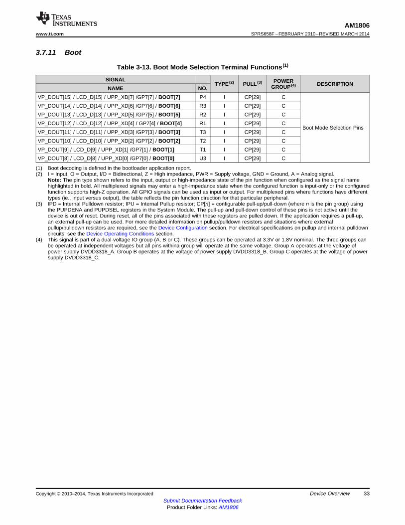
AM1806www.ti.com SPRS658F –FEBRUARY 2010–REVISED MARCH 2014
3.7.11 Boot
Table 3-13. Boot Mode Selection Terminal Functions (1)
SIGNAL POWERTYPE (2) PULL (3) DESCRIPTIONGROUP (4)NAME NO.VP_DOUT[15] / LCD_D[15] / UPP_XD[7] /GP7[7] / BOOT[7] P4 I CP[29] CVP_DOUT[14] / LCD_D[14] / UPP_XD[6] /GP7[6] / BOOT[6] R3 I CP[29] CVP_DOUT[13] / LCD_D[13] / UPP_XD[5] /GP7[5] / BOOT[5] R2 I CP[29] CVP_DOUT[12] / LCD_D[12] / UPP_XD[4] / GP7[4] / BOOT[4] R1 I CP[29] C
Boot Mode Selection PinsVP_DOUT[11] / LCD_D[11] / UPP_XD[3] /GP7[3] / BOOT[3] T3 I CP[29] CVP_DOUT[10] / LCD_D[10] / UPP_XD[2] /GP7[2] / BOOT[2] T2 I CP[29] CVP_DOUT[9] / LCD_D[9] / UPP_XD[1] /GP7[1] / BOOT[1] T1 I CP[29] CVP_DOUT[8] / LCD_D[8] / UPP_XD[0] /GP7[0] / BOOT[0] U3 I CP[29] C
(1) Boot decoding is defined in the bootloader application report.(2) I = Input, O = Output, I/O = Bidirectional, Z = High impedance, PWR = Supply voltage, GND = Ground, A = Analog signal.
Note: The pin type shown refers to the input, output or high-impedance state of the pin function when configured as the signal namehighlighted in bold. All multiplexed signals may enter a high-impedance state when the configured function is input-only or the configuredfunction supports high-Z operation. All GPIO signals can be used as input or output. For multiplexed pins where functions have differenttypes (ie., input versus output), the table reflects the pin function direction for that particular peripheral.
(3) IPD = Internal Pulldown resistor; IPU = Internal Pullup resistor; CP[n] = configurable pull-up/pull-down (where n is the pin group) usingthe PUPDENA and PUPDSEL registers in the System Module. The pull-up and pull-down control of these pins is not active until thedevice is out of reset. During reset, all of the pins associated with these registers are pulled down. If the application requires a pull-up,an external pull-up can be used. For more detailed information on pullup/pulldown resistors and situations where externalpullup/pulldown resistors are required, see the Device Configuration section. For electrical specifications on pullup and internal pulldowncircuits, see the Device Operating Conditions section.
(4) This signal is part of a dual-voltage IO group (A, B or C). These groups can be operated at 3.3V or 1.8V nominal. The three groups canbe operated at independent voltages but all pins withina group will operate at the same voltage. Group A operates at the voltage ofpower supply DVDD3318_A. Group B operates at the voltage of power supply DVDD3318_B. Group C operates at the voltage of powersupply DVDD3318_C.
Copyright © 2010–2014, Texas Instruments Incorporated Device Overview 33Submit Documentation Feedback
Product Folder Links: AM1806
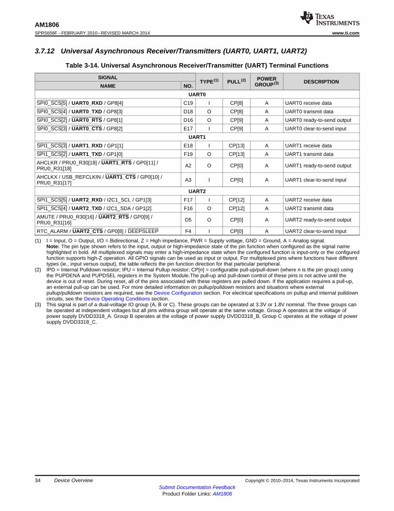
AM1806SPRS658F –FEBRUARY 2010–REVISED MARCH 2014 www.ti.com
3.7.12 Universal Asynchronous Receiver/Transmitters (UART0, UART1, UART2)
Table 3-14. Universal Asynchronous Receiver/Transmitter (UART) Terminal Functions
SIGNAL POWERTYPE (1) PULL (2) DESCRIPTIONGROUP (3)NAME NO.UART0
SPI0_SCS[5] / UART0_RXD / GP8[4] C19 I CP[8] A UART0 receive dataSPI0_SCS[4] / UART0_TXD / GP8[3] D18 O CP[8] A UART0 transmit dataSPI0_SCS[2] / UART0_RTS / GP8[1] D16 O CP[9] A UART0 ready-to-send outputSPI0_SCS[3] / UART0_CTS / GP8[2] E17 I CP[9] A UART0 clear-to-send input
UART1SPI1_SCS[3] / UART1_RXD / GP1[1] E18 I CP[13] A UART1 receive dataSPI1_SCS[2] / UART1_TXD / GP1[0] F19 O CP[13] A UART1 transmit dataAHCLKR / PRU0_R30[18] / UART1_RTS / GP0[11] / A2 O CP[0] A UART1 ready-to-send outputPRU0_R31[18]AHCLKX / USB_REFCLKIN / UART1_CTS / GP0[10] / A3 I CP[0] A UART1 clear-to-send inputPRU0_R31[17]
UART2SPI1_SCS[5] / UART2_RXD / I2C1_SCL / GP1[3] F17 I CP[12] A UART2 receive dataSPI1_SCS[4] / UART2_TXD / I2C1_SDA / GP1[2] F16 O CP[12] A UART2 transmit dataAMUTE / PRU0_R30[16] / UART2_RTS / GP0[9] / D5 O CP[0] A UART2 ready-to-send outputPRU0_R31[16]RTC_ALARM / UART2_CTS / GP0[8] / DEEPSLEEP F4 I CP[0] A UART2 clear-to-send input
(1) I = Input, O = Output, I/O = Bidirectional, Z = High impedance, PWR = Supply voltage, GND = Ground, A = Analog signal.Note: The pin type shown refers to the input, output or high-impedance state of the pin function when configured as the signal namehighlighted in bold. All multiplexed signals may enter a high-impedance state when the configured function is input-only or the configuredfunction supports high-Z operation. All GPIO signals can be used as input or output. For multiplexed pins where functions have differenttypes (ie., input versus output), the table reflects the pin function direction for that particular peripheral.
(2) IPD = Internal Pulldown resistor; IPU = Internal Pullup resistor; CP[n] = configurable pull-up/pull-down (where n is the pin group) usingthe PUPDENA and PUPDSEL registers in the System Module.The pull-up and pull-down control of these pins is not active until thedevice is out of reset. During reset, all of the pins associated with these registers are pulled down. If the application requires a pull-up,an external pull-up can be used. For more detailed information on pullup/pulldown resistors and situations where externalpullup/pulldown resistors are required, see the Device Configuration section. For electrical specifications on pullup and internal pulldowncircuits, see the Device Operating Conditions section.
(3) This signal is part of a dual-voltage IO group (A, B or C). These groups can be operated at 3.3V or 1.8V nominal. The three groups canbe operated at independent voltages but all pins withina group will operate at the same voltage. Group A operates at the voltage ofpower supply DVDD3318_A. Group B operates at the voltage of power supply DVDD3318_B. Group C operates at the voltage of powersupply DVDD3318_C.
34 Device Overview Copyright © 2010–2014, Texas Instruments IncorporatedSubmit Documentation Feedback
Product Folder Links: AM1806
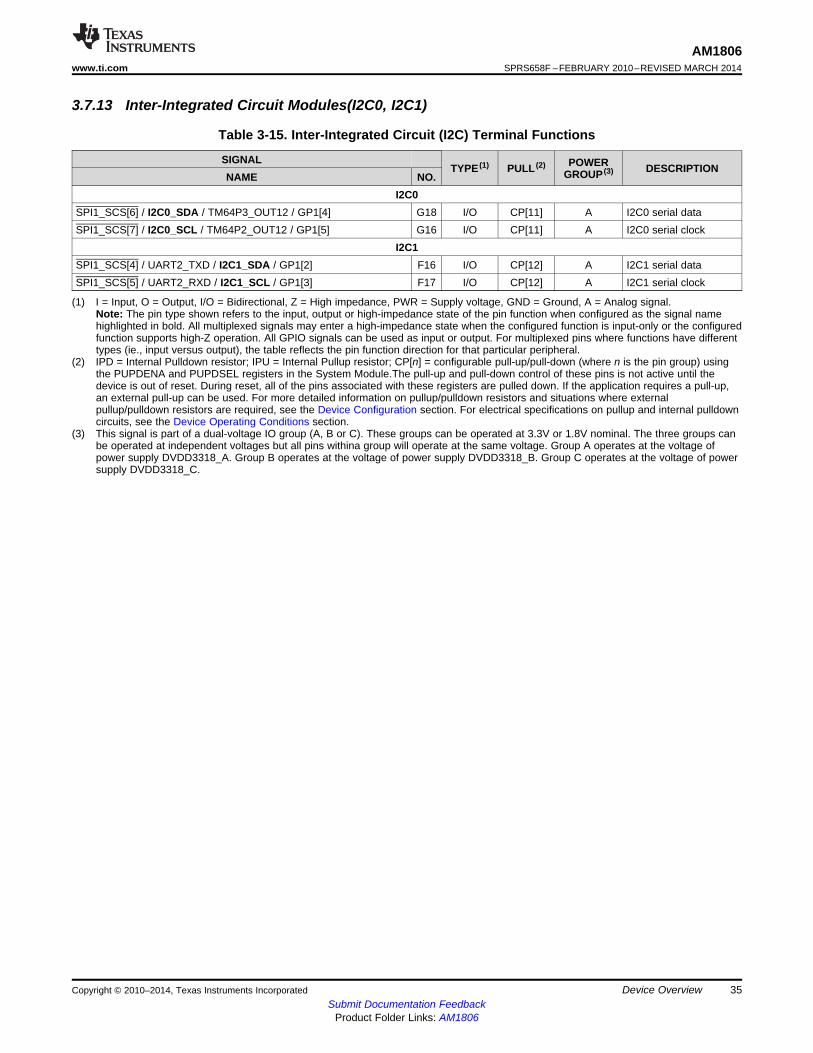
AM1806www.ti.com SPRS658F –FEBRUARY 2010–REVISED MARCH 2014
3.7.13 Inter-Integrated Circuit Modules(I2C0, I2C1)
Table 3-15. Inter-Integrated Circuit (I2C) Terminal Functions
SIGNAL POWERTYPE (1) PULL (2) DESCRIPTIONGROUP (3)NAME NO.I2C0
SPI1_SCS[6] / I2C0_SDA / TM64P3_OUT12 / GP1[4] G18 I/O CP[11] A I2C0 serial dataSPI1_SCS[7] / I2C0_SCL / TM64P2_OUT12 / GP1[5] G16 I/O CP[11] A I2C0 serial clock
I2C1SPI1_SCS[4] / UART2_TXD / I2C1_SDA / GP1[2] F16 I/O CP[12] A I2C1 serial dataSPI1_SCS[5] / UART2_RXD / I2C1_SCL / GP1[3] F17 I/O CP[12] A I2C1 serial clock
(1) I = Input, O = Output, I/O = Bidirectional, Z = High impedance, PWR = Supply voltage, GND = Ground, A = Analog signal.Note: The pin type shown refers to the input, output or high-impedance state of the pin function when configured as the signal namehighlighted in bold. All multiplexed signals may enter a high-impedance state when the configured function is input-only or the configuredfunction supports high-Z operation. All GPIO signals can be used as input or output. For multiplexed pins where functions have differenttypes (ie., input versus output), the table reflects the pin function direction for that particular peripheral.
(2) IPD = Internal Pulldown resistor; IPU = Internal Pullup resistor; CP[n] = configurable pull-up/pull-down (where n is the pin group) usingthe PUPDENA and PUPDSEL registers in the System Module.The pull-up and pull-down control of these pins is not active until thedevice is out of reset. During reset, all of the pins associated with these registers are pulled down. If the application requires a pull-up,an external pull-up can be used. For more detailed information on pullup/pulldown resistors and situations where externalpullup/pulldown resistors are required, see the Device Configuration section. For electrical specifications on pullup and internal pulldowncircuits, see the Device Operating Conditions section.
(3) This signal is part of a dual-voltage IO group (A, B or C). These groups can be operated at 3.3V or 1.8V nominal. The three groups canbe operated at independent voltages but all pins withina group will operate at the same voltage. Group A operates at the voltage ofpower supply DVDD3318_A. Group B operates at the voltage of power supply DVDD3318_B. Group C operates at the voltage of powersupply DVDD3318_C.
Copyright © 2010–2014, Texas Instruments Incorporated Device Overview 35Submit Documentation Feedback
Product Folder Links: AM1806
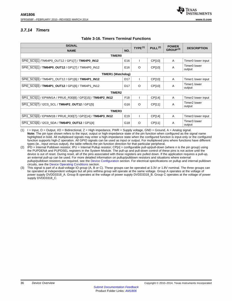
AM1806SPRS658F –FEBRUARY 2010–REVISED MARCH 2014 www.ti.com
3.7.14 Timers
Table 3-16. Timers Terminal Functions
SIGNAL POWERTYPE (1) PULL (2) DESCRIPTIONGROUP (3)NAME NO.TIMER0
SPI0_SCS[1] /TM64P0_OUT12 / GP1[7] / TM64P0_IN12 E16 I CP[10] A Timer0 lower inputTimer0 lowerSPI0_SCS[1] / TM64P0_OUT12 / GP1[7] / TM64P0_IN12 E16 O CP[10] A output
TIMER1 (Watchdog)SPI0_SCS[0] / TM64P1_OUT12 / GP1[6] / TM64P1_IN12 D17 I CP[10] A Timer1 lower input
Timer1 lowerSPI0_SCS[0] / TM64P1_OUT12 / GP1[6] / TM64P1_IN12 D17 O CP[10] A outputTIMER2
SPI1_SCS[1] / EPWM1A / PRU0_R30[8] / GP2[15] / TM64P2_IN12 F18 I CP[14] A Timer2 lower inputTimer2 lowerSPI1_SCS[7] / I2C0_SCL / TM64P2_OUT12 / GP1[5] G16 O CP[11] A output
TIMER3SPI1_SCS[0] / EPWM1B / PRU0_R30[7] / GP2[14] / TM64P3_IN12 E19 I CP[14] A Timer3 lower input
Timer3 lowerSPI1_SCS[6] / I2C0_SDA / TM64P3_OUT12 / GP1[4] G18 O CP[11] A output
(1) I = Input, O = Output, I/O = Bidirectional, Z = High impedance, PWR = Supply voltage, GND = Ground, A = Analog signal.Note: The pin type shown refers to the input, output or high-impedance state of the pin function when configured as the signal namehighlighted in bold. All multiplexed signals may enter a high-impedance state when the configured function is input-only or the configuredfunction supports high-Z operation. All GPIO signals can be used as input or output. For multiplexed pins where functions have differenttypes (ie., input versus output), the table reflects the pin function direction for that particular peripheral.
(2) IPD = Internal Pulldown resistor; IPU = Internal Pullup resistor; CP[n] = configurable pull-up/pull-down (where n is the pin group) usingthe PUPDENA and PUPDSEL registers in the System Module. The pull-up and pull-down control of these pins is not active until thedevice is out of reset. During reset, all of the pins associated with these registers are pulled down. If the application requires a pull-up,an external pull-up can be used. For more detailed information on pullup/pulldown resistors and situations where externalpullup/pulldown resistors are required, see the Device Configuration section. For electrical specifications on pullup and internal pulldowncircuits, see the Device Operating Conditions section.
(3) This signal is part of a dual-voltage IO group (A, B or C). These groups can be operated at 3.3V or 1.8V nominal. The three groups canbe operated at independent voltages but all pins withina group will operate at the same voltage. Group A operates at the voltage ofpower supply DVDD3318_A. Group B operates at the voltage of power supply DVDD3318_B. Group C operates at the voltage of powersupply DVDD3318_C.
36 Device Overview Copyright © 2010–2014, Texas Instruments IncorporatedSubmit Documentation Feedback
Product Folder Links: AM1806
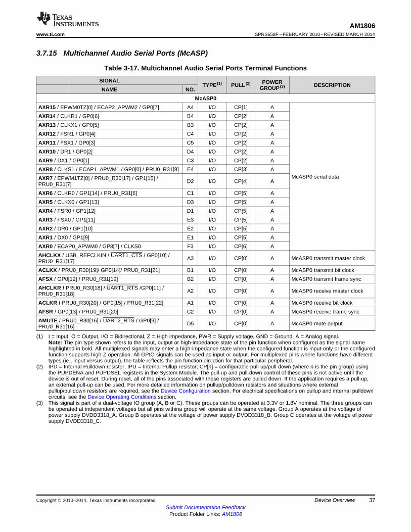
AM1806www.ti.com SPRS658F –FEBRUARY 2010–REVISED MARCH 2014
3.7.15 Multichannel Audio Serial Ports (McASP)
Table 3-17. Multichannel Audio Serial Ports Terminal Functions
SIGNAL POWERTYPE (1) PULL (2) DESCRIPTIONGROUP (3)NAME NO.McASP0
AXR15 / EPWM0TZ[0] / ECAP2_APWM2 / GP0[7] A4 I/O CP[1] AAXR14 / CLKR1 / GP0[6] B4 I/O CP[2] AAXR13 / CLKX1 / GP0[5] B3 I/O CP[2] AAXR12 / FSR1 / GP0[4] C4 I/O CP[2] AAXR11 / FSX1 / GP0[3] C5 I/O CP[2] AAXR10 / DR1 / GP0[2] D4 I/O CP[2] AAXR9 / DX1 / GP0[1] C3 I/O CP[2] AAXR8 / CLKS1 / ECAP1_APWM1 / GP0[0] / PRU0_R31[8] E4 I/O CP[3] A
McASP0 serial dataAXR7 / EPWM1TZ[0] / PRU0_R30[17] / GP1[15] / D2 I/O CP[4] APRU0_R31[7]AXR6 / CLKR0 / GP1[14] / PRU0_R31[6] C1 I/O CP[5] AAXR5 / CLKX0 / GP1[13] D3 I/O CP[5] AAXR4 / FSR0 / GP1[12] D1 I/O CP[5] AAXR3 / FSX0 / GP1[11] E3 I/O CP[5] AAXR2 / DR0 / GP1[10] E2 I/O CP[5] AAXR1 / DX0 / GP1[9] E1 I/O CP[5] AAXR0 / ECAP0_APWM0 / GP8[7] / CLKS0 F3 I/O CP[6] AAHCLKX / USB_REFCLKIN / UART1_CTS / GP0[10] / A3 I/O CP[0] A McASP0 transmit master clockPRU0_R31[17]ACLKX / PRU0_R30[19]/ GP0[14]/ PRU0_R31[21] B1 I/O CP[0] A McASP0 transmit bit clockAFSX / GP0[12] / PRU0_R31[19] B2 I/O CP[0] A McASP0 transmit frame syncAHCLKR / PRU0_R30[18] / UART1_RTS /GP0[11] / A2 I/O CP[0] A McASP0 receive master clockPRU0_R31[18]ACLKR / PRU0_R30[20] / GP0[15] / PRU0_R31[22] A1 I/O CP[0] A McASP0 receive bit clockAFSR / GP0[13] / PRU0_R31[20] C2 I/O CP[0] A McASP0 receive frame syncAMUTE / PRU0_R30[16] / UART2_RTS / GP0[9] / D5 I/O CP[0] A McASP0 mute outputPRU0_R31[16]
(1) I = Input, O = Output, I/O = Bidirectional, Z = High impedance, PWR = Supply voltage, GND = Ground, A = Analog signal.Note: The pin type shown refers to the input, output or high-impedance state of the pin function when configured as the signal namehighlighted in bold. All multiplexed signals may enter a high-impedance state when the configured function is input-only or the configuredfunction supports high-Z operation. All GPIO signals can be used as input or output. For multiplexed pins where functions have differenttypes (ie., input versus output), the table reflects the pin function direction for that particular peripheral.
(2) IPD = Internal Pulldown resistor; IPU = Internal Pullup resistor; CP[n] = configurable pull-up/pull-down (where n is the pin group) usingthe PUPDENA and PUPDSEL registers in the System Module. The pull-up and pull-down control of these pins is not active until thedevice is out of reset. During reset, all of the pins associated with these registers are pulled down. If the application requires a pull-up,an external pull-up can be used. For more detailed information on pullup/pulldown resistors and situations where externalpullup/pulldown resistors are required, see the Device Configuration section. For electrical specifications on pullup and internal pulldowncircuits, see the Device Operating Conditions section.
(3) This signal is part of a dual-voltage IO group (A, B or C). These groups can be operated at 3.3V or 1.8V nominal. The three groups canbe operated at independent voltages but all pins withina group will operate at the same voltage. Group A operates at the voltage ofpower supply DVDD3318_A. Group B operates at the voltage of power supply DVDD3318_B. Group C operates at the voltage of powersupply DVDD3318_C.
Copyright © 2010–2014, Texas Instruments Incorporated Device Overview 37Submit Documentation Feedback
Product Folder Links: AM1806
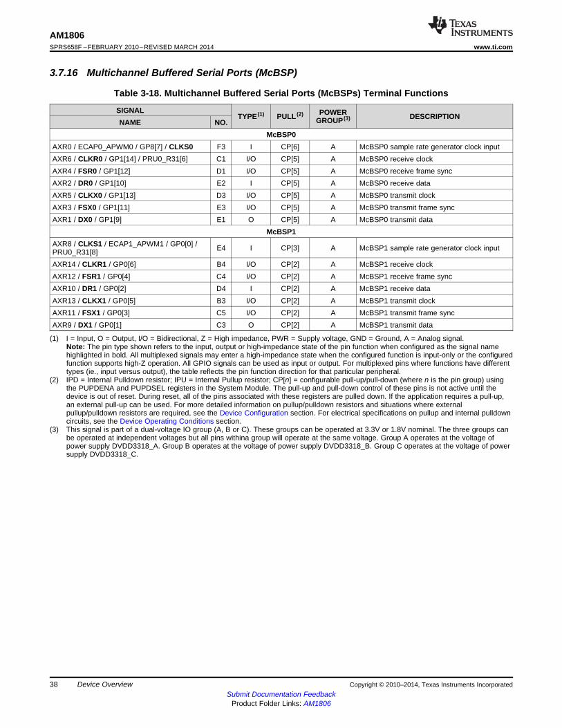
AM1806SPRS658F –FEBRUARY 2010–REVISED MARCH 2014 www.ti.com
3.7.16 Multichannel Buffered Serial Ports (McBSP)
Table 3-18. Multichannel Buffered Serial Ports (McBSPs) Terminal Functions
SIGNAL POWERTYPE (1) PULL (2) DESCRIPTIONGROUP (3)NAME NO.McBSP0
AXR0 / ECAP0_APWM0 / GP8[7] / CLKS0 F3 I CP[6] A McBSP0 sample rate generator clock inputAXR6 / CLKR0 / GP1[14] / PRU0_R31[6] C1 I/O CP[5] A McBSP0 receive clockAXR4 / FSR0 / GP1[12] D1 I/O CP[5] A McBSP0 receive frame syncAXR2 / DR0 / GP1[10] E2 I CP[5] A McBSP0 receive dataAXR5 / CLKX0 / GP1[13] D3 I/O CP[5] A McBSP0 transmit clockAXR3 / FSX0 / GP1[11] E3 I/O CP[5] A McBSP0 transmit frame syncAXR1 / DX0 / GP1[9] E1 O CP[5] A McBSP0 transmit data
McBSP1AXR8 / CLKS1 / ECAP1_APWM1 / GP0[0] / E4 I CP[3] A McBSP1 sample rate generator clock inputPRU0_R31[8]AXR14 / CLKR1 / GP0[6] B4 I/O CP[2] A McBSP1 receive clockAXR12 / FSR1 / GP0[4] C4 I/O CP[2] A McBSP1 receive frame syncAXR10 / DR1 / GP0[2] D4 I CP[2] A McBSP1 receive dataAXR13 / CLKX1 / GP0[5] B3 I/O CP[2] A McBSP1 transmit clockAXR11 / FSX1 / GP0[3] C5 I/O CP[2] A McBSP1 transmit frame syncAXR9 / DX1 / GP0[1] C3 O CP[2] A McBSP1 transmit data
(1) I = Input, O = Output, I/O = Bidirectional, Z = High impedance, PWR = Supply voltage, GND = Ground, A = Analog signal.Note: The pin type shown refers to the input, output or high-impedance state of the pin function when configured as the signal namehighlighted in bold. All multiplexed signals may enter a high-impedance state when the configured function is input-only or the configuredfunction supports high-Z operation. All GPIO signals can be used as input or output. For multiplexed pins where functions have differenttypes (ie., input versus output), the table reflects the pin function direction for that particular peripheral.
(2) IPD = Internal Pulldown resistor; IPU = Internal Pullup resistor; CP[n] = configurable pull-up/pull-down (where n is the pin group) usingthe PUPDENA and PUPDSEL registers in the System Module. The pull-up and pull-down control of these pins is not active until thedevice is out of reset. During reset, all of the pins associated with these registers are pulled down. If the application requires a pull-up,an external pull-up can be used. For more detailed information on pullup/pulldown resistors and situations where externalpullup/pulldown resistors are required, see the Device Configuration section. For electrical specifications on pullup and internal pulldowncircuits, see the Device Operating Conditions section.
(3) This signal is part of a dual-voltage IO group (A, B or C). These groups can be operated at 3.3V or 1.8V nominal. The three groups canbe operated at independent voltages but all pins withina group will operate at the same voltage. Group A operates at the voltage ofpower supply DVDD3318_A. Group B operates at the voltage of power supply DVDD3318_B. Group C operates at the voltage of powersupply DVDD3318_C.
38 Device Overview Copyright © 2010–2014, Texas Instruments IncorporatedSubmit Documentation Feedback
Product Folder Links: AM1806
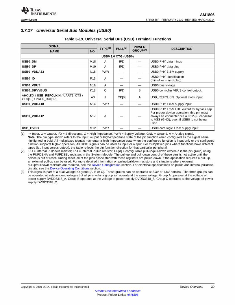
AM1806www.ti.com SPRS658F –FEBRUARY 2010–REVISED MARCH 2014
3.7.17 Universal Serial Bus Modules (USB0)
Table 3-19. Universal Serial Bus (USB) Terminal Functions
SIGNAL POWERTYPE (1) PULL (2) DESCRIPTIONGROUP (3)NAME NO.USB0 2.0 OTG (USB0)
USB0_DM M18 A IPD — USB0 PHY data minusUSB0_DP M19 A IPD — USB0 PHY data plusUSB0_VDDA33 N18 PWR — — USB0 PHY 3.3-V supply
USB0 PHY identificationUSB0_ID P16 A — — (mini-A or mini-B plug)USB0_VBUS N19 A — — USB0 bus voltageUSB0_DRVVBUS K18 O IPD B USB0 controller VBUS control output.AHCLKX / USB_REFCLKIN / UART1_CTS / A3 I CP[0] A USB_REFCLKIN. Optional clock inputGP0[10] / PRU0_R31[17]USB0_VDDA18 N14 PWR — — USB0 PHY 1.8-V supply input
USB0 PHY 1.2-V LDO output for bypass capFor proper device operation, this pin must
USB0_VDDA12 N17 A — — always be connected via a 0.22-μF capacitorto VSS (GND), even if USB0 is not beingused.
USB_CVDD M12 PWR — — USB0 core logic 1.2-V supply input
(1) I = Input, O = Output, I/O = Bidirectional, Z = High impedance, PWR = Supply voltage, GND = Ground, A = Analog signal.Note: The pin type shown refers to the input, output or high-impedance state of the pin function when configured as the signal namehighlighted in bold. All multiplexed signals may enter a high-impedance state when the configured function is input-only or the configuredfunction supports high-Z operation. All GPIO signals can be used as input or output. For multiplexed pins where functions have differenttypes (ie., input versus output), the table reflects the pin function direction for that particular peripheral.
(2) IPD = Internal Pulldown resistor; IPU = Internal Pullup resistor; CP[n] = configurable pull-up/pull-down (where n is the pin group) usingthe PUPDENA and PUPDSEL registers in the System Module. The pull-up and pull-down control of these pins is not active until thedevice is out of reset. During reset, all of the pins associated with these registers are pulled down. If the application requires a pull-up,an external pull-up can be used. For more detailed information on pullup/pulldown resistors and situations where externalpullup/pulldown resistors are required, see the Device Configuration section. For electrical specifications on pullup and internal pulldowncircuits, see the Device Operating Conditions section.
(3) This signal is part of a dual-voltage IO group (A, B or C). These groups can be operated at 3.3V or 1.8V nominal. The three groups canbe operated at independent voltages but all pins withina group will operate at the same voltage. Group A operates at the voltage ofpower supply DVDD3318_A. Group B operates at the voltage of power supply DVDD3318_B. Group C operates at the voltage of powersupply DVDD3318_C.
Copyright © 2010–2014, Texas Instruments Incorporated Device Overview 39Submit Documentation Feedback
Product Folder Links: AM1806
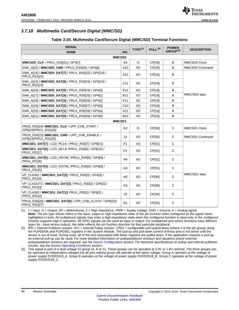
AM1806SPRS658F –FEBRUARY 2010–REVISED MARCH 2014 www.ti.com
3.7.18 Multimedia Card/Secure Digital (MMC/SD)
Table 3-20. Multimedia Card/Secure Digital (MMC/SD) Terminal Functions
SIGNAL POWERTYPE (1) PULL (2) DESCRIPTIONGROUP (3)NAME NO.MMCSD0
MMCSD0_CLK / PRU1_R30[31] / GP4[7] E9 O CP[18] B MMCSD0 ClockEMA_A[22] / MMCSD0_CMD / PRU1_R30[30] / GP4[6] A10 I/O CP[18] B MMCSD0 CommandEMA_A[14] / MMCSD0_DAT[7] / PRU1_R30[22] / GP5[14] / A12 I/O CP[19] BPRU1_R31[22]EMA_A[15] / MMCSD0_DAT[6] / PRU1_R30[23] / GP5[15] / C11 I/O CP[19] BPRU1_R31[23]EMA_A[16] / MMCSD0_DAT[5] / PRU1_R30[24] / GP4[0] E12 I/O CP[18] B
MMC/SD0 dataEMA_A[17] / MMCSD0_DAT[4] / PRU1_R30[25] / GP4[1] B11 I/O CP[18] BEMA_A[18] / MMCSD0_DAT[3] / PRU1_R30[26] / GP4[2] E11 I/O CP[18] BEMA_A[19] / MMCSD0_DAT[2] / PRU1_R30[27] / GP4[3] C10 I/O CP[18] BEMA_A[20] / MMCSD0_DAT[1] / PRU1_R30[28] / GP4[4] A11 I/O CP[18] BEMA_A[21] / MMCSD0_DAT[0] / PRU1_R30[29] / GP4[5] B10 I/O CP[18] B
MMCSD1PRU0_R30[24] /MMCSD1_CLK / UPP_CHB_START / G2 O CP[30] C MMCSD1 ClockGP8[14]/PRU1_R31[26]/PRU0_R30[23] /MMCSD1_CMD / UPP_CHB_ENABLE / J4 I/O CP[30] C MMCSD1 CommandGP8[13]/PRU1_R31[25]MMCSD1_DAT[7] / LCD_PCLK / PRU1_R30[7] / GP8[11] F1 I/O CP[31] CMMCSD1_DAT[6] / LCD_MCLK /PRU1_R30[6] / GP8[10] / F2 I/O CP[31] CPRU1_R31[7]MMCSD1_DAT[5] / LCD_HSYNC /PRU1_R30[5] / GP8[9] / H4 I/O CP[31] CPRU1_R31[6]MMCSD1_DAT[4] / LCD_VSYNC /PRU1_R30[4] / GP8[8] / G4 I/O CP[31] CPRU1_R31[5]
MMC/SD1 dataVP_CLKIN2 / MMCSD1_DAT[3] / PRU1_R30[3] / GP6[4] / H3 I/O CP[30] CPRU1_R31[4]VP_CLKOUT2 / MMCSD1_DAT[2] / PRU1_R30[2] / GP6[3] / K3 I/O CP[30] CPRU1_R31[3]VP_CLKIN3 / MMCSD1_DAT[1]/ PRU1_R30[1] / GP6[2] / J3 I/O CP[30] CPRU1_R31[2]PRU0_R30[25] / MMCSD1_DAT[0] / UPP_CHB_CLOCK / GP8[15]/ G1 I/O CP[30] CPRU1_R31[27]
(1) I = Input, O = Output, I/O = Bidirectional, Z = High impedance, PWR = Supply voltage, GND = Ground, A = Analog signal.Note: The pin type shown refers to the input, output or high-impedance state of the pin function when configured as the signal namehighlighted in bold. All multiplexed signals may enter a high-impedance state when the configured function is input-only or the configuredfunction supports high-Z operation. All GPIO signals can be used as input or output. For multiplexed pins where functions have differenttypes (ie., input versus output), the table reflects the pin function direction for that particular peripheral.
(2) IPD = Internal Pulldown resistor; IPU = Internal Pullup resistor; CP[n] = configurable pull-up/pull-down (where n is the pin group) usingthe PUPDENA and PUPDSEL registers in the System Module. The pull-up and pull-down control of these pins is not active until thedevice is out of reset. During reset, all of the pins associated with these registers are pulled down. If the application requires a pull-up,an external pull-up can be used. For more detailed information on pullup/pulldown resistors and situations where externalpullup/pulldown resistors are required, see the Device Configuration section. For electrical specifications on pullup and internal pulldowncircuits, see the Device Operating Conditions section.
(3) This signal is part of a dual-voltage IO group (A, B or C). These groups can be operated at 3.3V or 1.8V nominal. The three groups canbe operated at independent voltages but all pins withina group will operate at the same voltage. Group A operates at the voltage ofpower supply DVDD3318_A. Group B operates at the voltage of power supply DVDD3318_B. Group C operates at the voltage of powersupply DVDD3318_C.
40 Device Overview Copyright © 2010–2014, Texas Instruments IncorporatedSubmit Documentation Feedback
Product Folder Links: AM1806
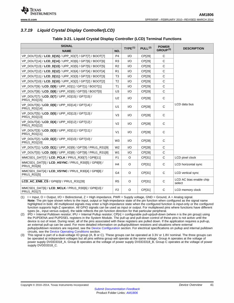
AM1806www.ti.com SPRS658F –FEBRUARY 2010–REVISED MARCH 2014
3.7.19 Liquid Crystal Display Controller(LCD)
Table 3-21. Liquid Crystal Display Controller (LCD) Terminal Functions
SIGNAL POWERTYPE (1) PULL (2) DESCRIPTIONGROUP (3)NAME NO.VP_DOUT[15] / LCD_D[15] / UPP_XD[7] / GP7[7] / BOOT[7] P4 I/O CP[29] CVP_DOUT[14] / LCD_D[14] / UPP_XD[6] / GP7[6] / BOOT[6] R3 I/O CP[29] CVP_DOUT[13] / LCD_D[13] / UPP_XD[5] / GP7[5] / BOOT[5] R2 I/O CP[29] CVP_DOUT[12] / LCD_D[12] / UPP_XD[4] / GP7[4] / BOOT[4] R1 I/O CP[29] CVP_DOUT[11] / LCD_D[11] / UPP_XD[3] / GP7[3] / BOOT[3] T3 I/O CP[29] CVP_DOUT[10] / LCD_D[10] / UPP_XD[2] / GP7[2] / BOOT[2] T2 I/O CP[29] CVP_DOUT[9] / LCD_D[9] / UPP_XD[1] / GP7[1] / BOOT[1] T1 I/O CP[29] CVP_DOUT[8] / LCD_D[8] / UPP_XD[0] / GP7[0] / BOOT[0] U3 I/O CP[29] CVP_DOUT[7] / LCD_D[7] / UPP_XD[15] / GP7[15] / U2 I/O CP[28] CPRU1_R31[15]
LCD data busVP_DOUT[6] / LCD_D[6] / UPP_XD[14] / GP7[14] / U1 I/O CP[28] CPRU1_R31[14]VP_DOUT[5] / LCD_D[5] / UPP_XD[13] / GP7[13] / V3 I/O CP[28] CPRU1_R31[13]VP_DOUT[4] / LCD_D[4] / UPP_XD[12] / GP7[12] / V2 I/O CP[28] CPRU1_R31[12]VP_DOUT[3] / LCD_D[3] / UPP_XD[11] / GP7[11] / V1 I/O CP[28] CPRU1_R31[11]VP_DOUT[2] / LCD_D[2] / UPP_XD[10] / GP7[10] / W3 I/O CP[28] CPRU1_R31[10]VP_DOUT[1] / LCD_D[1] / UPP_XD[9] / GP7[9] / PRU1_R31[9] W2 I/O CP[28] CVP_DOUT[0] / LCD_D[0] / UPP_XD[8] / GP7[8] / PRU1_R31[8] W1 I/O CP[28] CMMCSD1_DAT[7] / LCD_PCLK / PRU1_R30[7] / GP8[11] F1 O CP[31] C LCD pixel clockMMCSD1_DAT[5] / LCD_HSYNC / PRU1_R30[5] / GP8[9] / H4 O CP[31] C LCD horizontal syncPRU1_R31[6]MMCSD1_DAT[4] / LCD_VSYNC / PRU1_R30[4] / GP8[8] / G4 O CP[31] C LCD vertical syncPRU1_R31[5]
LCD AC bias enable chipLCD_AC_ENB_CS / GP6[0]/ / PRU1_R31[28] R5 O CP[31] C selectMMCSD1_DAT[6] / LCD_MCLK / PRU1_R30[6] / GP8[10] / F2 O CP[31] C LCD memory clockPRU1_R31[7]
(1) I = Input, O = Output, I/O = Bidirectional, Z = High impedance, PWR = Supply voltage, GND = Ground, A = Analog signal.Note: The pin type shown refers to the input, output or high-impedance state of the pin function when configured as the signal namehighlighted in bold. All multiplexed signals may enter a high-impedance state when the configured function is input-only or the configuredfunction supports high-Z operation. All GPIO signals can be used as input or output. For multiplexed pins where functions have differenttypes (ie., input versus output), the table reflects the pin function direction for that particular peripheral.
(2) IPD = Internal Pulldown resistor; IPU = Internal Pullup resistor; CP[n] = configurable pull-up/pull-down (where n is the pin group) usingthe PUPDENA and PUPDSEL registers in the System Module. The pull-up and pull-down control of these pins is not active until thedevice is out of reset. During reset, all of the pins associated with these registers are pulled down. If the application requires a pull-up,an external pull-up can be used. For more detailed information on pullup/pulldown resistors and situations where externalpullup/pulldown resistors are required, see the Device Configuration section. For electrical specifications on pullup and internal pulldowncircuits, see the Device Operating Conditions section.
(3) This signal is part of a dual-voltage IO group (A, B or C). These groups can be operated at 3.3V or 1.8V nominal. The three groups canbe operated at independent voltages but all pins withina group will operate at the same voltage. Group A operates at the voltage ofpower supply DVDD3318_A. Group B operates at the voltage of power supply DVDD3318_B. Group C operates at the voltage of powersupply DVDD3318_C.
Copyright © 2010–2014, Texas Instruments Incorporated Device Overview 41Submit Documentation Feedback
Product Folder Links: AM1806
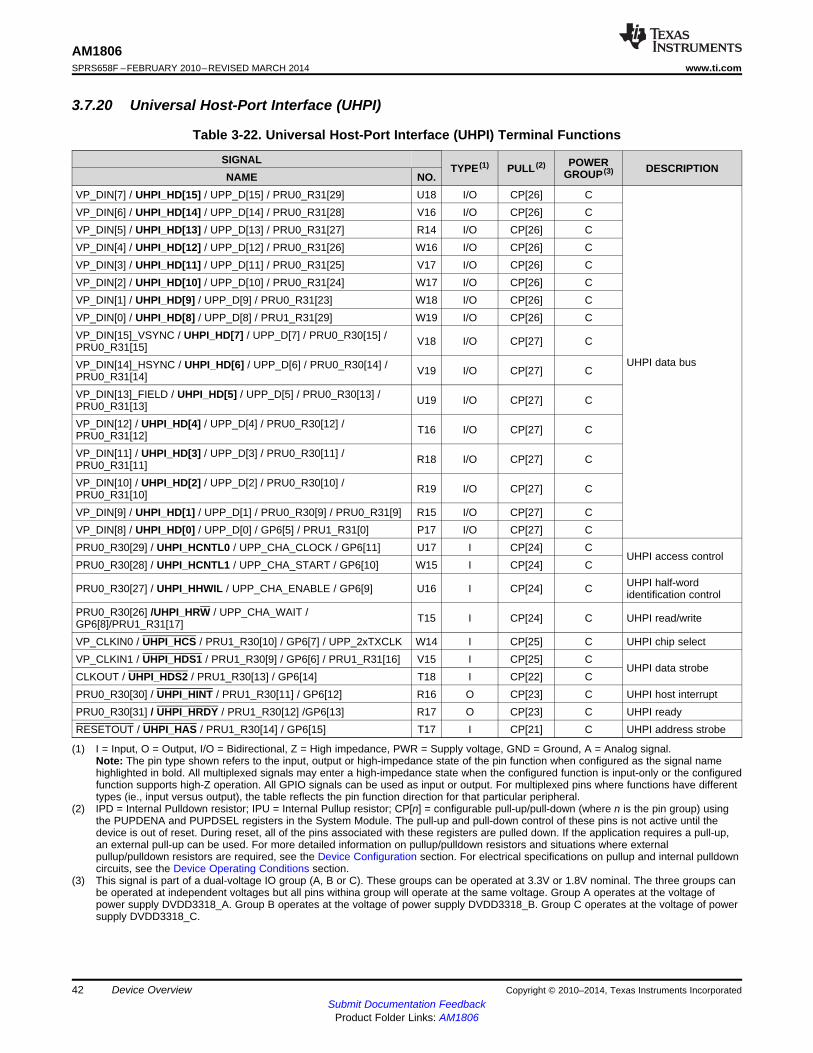
AM1806SPRS658F –FEBRUARY 2010–REVISED MARCH 2014 www.ti.com
3.7.20 Universal Host-Port Interface (UHPI)
Table 3-22. Universal Host-Port Interface (UHPI) Terminal Functions
SIGNAL POWERTYPE (1) PULL (2) DESCRIPTIONGROUP (3)NAME NO.VP_DIN[7] / UHPI_HD[15] / UPP_D[15] / PRU0_R31[29] U18 I/O CP[26] CVP_DIN[6] / UHPI_HD[14] / UPP_D[14] / PRU0_R31[28] V16 I/O CP[26] CVP_DIN[5] / UHPI_HD[13] / UPP_D[13] / PRU0_R31[27] R14 I/O CP[26] CVP_DIN[4] / UHPI_HD[12] / UPP_D[12] / PRU0_R31[26] W16 I/O CP[26] CVP_DIN[3] / UHPI_HD[11] / UPP_D[11] / PRU0_R31[25] V17 I/O CP[26] CVP_DIN[2] / UHPI_HD[10] / UPP_D[10] / PRU0_R31[24] W17 I/O CP[26] CVP_DIN[1] / UHPI_HD[9] / UPP_D[9] / PRU0_R31[23] W18 I/O CP[26] CVP_DIN[0] / UHPI_HD[8] / UPP_D[8] / PRU1_R31[29] W19 I/O CP[26] CVP_DIN[15]_VSYNC / UHPI_HD[7] / UPP_D[7] / PRU0_R30[15] / V18 I/O CP[27] CPRU0_R31[15]
UHPI data busVP_DIN[14]_HSYNC / UHPI_HD[6] / UPP_D[6] / PRU0_R30[14] / V19 I/O CP[27] CPRU0_R31[14]VP_DIN[13]_FIELD / UHPI_HD[5] / UPP_D[5] / PRU0_R30[13] / U19 I/O CP[27] CPRU0_R31[13]VP_DIN[12] / UHPI_HD[4] / UPP_D[4] / PRU0_R30[12] / T16 I/O CP[27] CPRU0_R31[12]VP_DIN[11] / UHPI_HD[3] / UPP_D[3] / PRU0_R30[11] / R18 I/O CP[27] CPRU0_R31[11]VP_DIN[10] / UHPI_HD[2] / UPP_D[2] / PRU0_R30[10] / R19 I/O CP[27] CPRU0_R31[10]VP_DIN[9] / UHPI_HD[1] / UPP_D[1] / PRU0_R30[9] / PRU0_R31[9] R15 I/O CP[27] CVP_DIN[8] / UHPI_HD[0] / UPP_D[0] / GP6[5] / PRU1_R31[0] P17 I/O CP[27] CPRU0_R30[29] / UHPI_HCNTL0 / UPP_CHA_CLOCK / GP6[11] U17 I CP[24] C
UHPI access controlPRU0_R30[28] / UHPI_HCNTL1 / UPP_CHA_START / GP6[10] W15 I CP[24] C
UHPI half-wordPRU0_R30[27] / UHPI_HHWIL / UPP_CHA_ENABLE / GP6[9] U16 I CP[24] C identification controlPRU0_R30[26] /UHPI_HRW / UPP_CHA_WAIT / T15 I CP[24] C UHPI read/writeGP6[8]/PRU1_R31[17]VP_CLKIN0 / UHPI_HCS / PRU1_R30[10] / GP6[7] / UPP_2xTXCLK W14 I CP[25] C UHPI chip selectVP_CLKIN1 / UHPI_HDS1 / PRU1_R30[9] / GP6[6] / PRU1_R31[16] V15 I CP[25] C
UHPI data strobeCLKOUT / UHPI_HDS2 / PRU1_R30[13] / GP6[14] T18 I CP[22] CPRU0_R30[30] / UHPI_HINT / PRU1_R30[11] / GP6[12] R16 O CP[23] C UHPI host interruptPRU0_R30[31] / UHPI_HRDY / PRU1_R30[12] /GP6[13] R17 O CP[23] C UHPI readyRESETOUT / UHPI_HAS / PRU1_R30[14] / GP6[15] T17 I CP[21] C UHPI address strobe
(1) I = Input, O = Output, I/O = Bidirectional, Z = High impedance, PWR = Supply voltage, GND = Ground, A = Analog signal.Note: The pin type shown refers to the input, output or high-impedance state of the pin function when configured as the signal namehighlighted in bold. All multiplexed signals may enter a high-impedance state when the configured function is input-only or the configuredfunction supports high-Z operation. All GPIO signals can be used as input or output. For multiplexed pins where functions have differenttypes (ie., input versus output), the table reflects the pin function direction for that particular peripheral.
(2) IPD = Internal Pulldown resistor; IPU = Internal Pullup resistor; CP[n] = configurable pull-up/pull-down (where n is the pin group) usingthe PUPDENA and PUPDSEL registers in the System Module. The pull-up and pull-down control of these pins is not active until thedevice is out of reset. During reset, all of the pins associated with these registers are pulled down. If the application requires a pull-up,an external pull-up can be used. For more detailed information on pullup/pulldown resistors and situations where externalpullup/pulldown resistors are required, see the Device Configuration section. For electrical specifications on pullup and internal pulldowncircuits, see the Device Operating Conditions section.
(3) This signal is part of a dual-voltage IO group (A, B or C). These groups can be operated at 3.3V or 1.8V nominal. The three groups canbe operated at independent voltages but all pins withina group will operate at the same voltage. Group A operates at the voltage ofpower supply DVDD3318_A. Group B operates at the voltage of power supply DVDD3318_B. Group C operates at the voltage of powersupply DVDD3318_C.
42 Device Overview Copyright © 2010–2014, Texas Instruments IncorporatedSubmit Documentation Feedback
Product Folder Links: AM1806
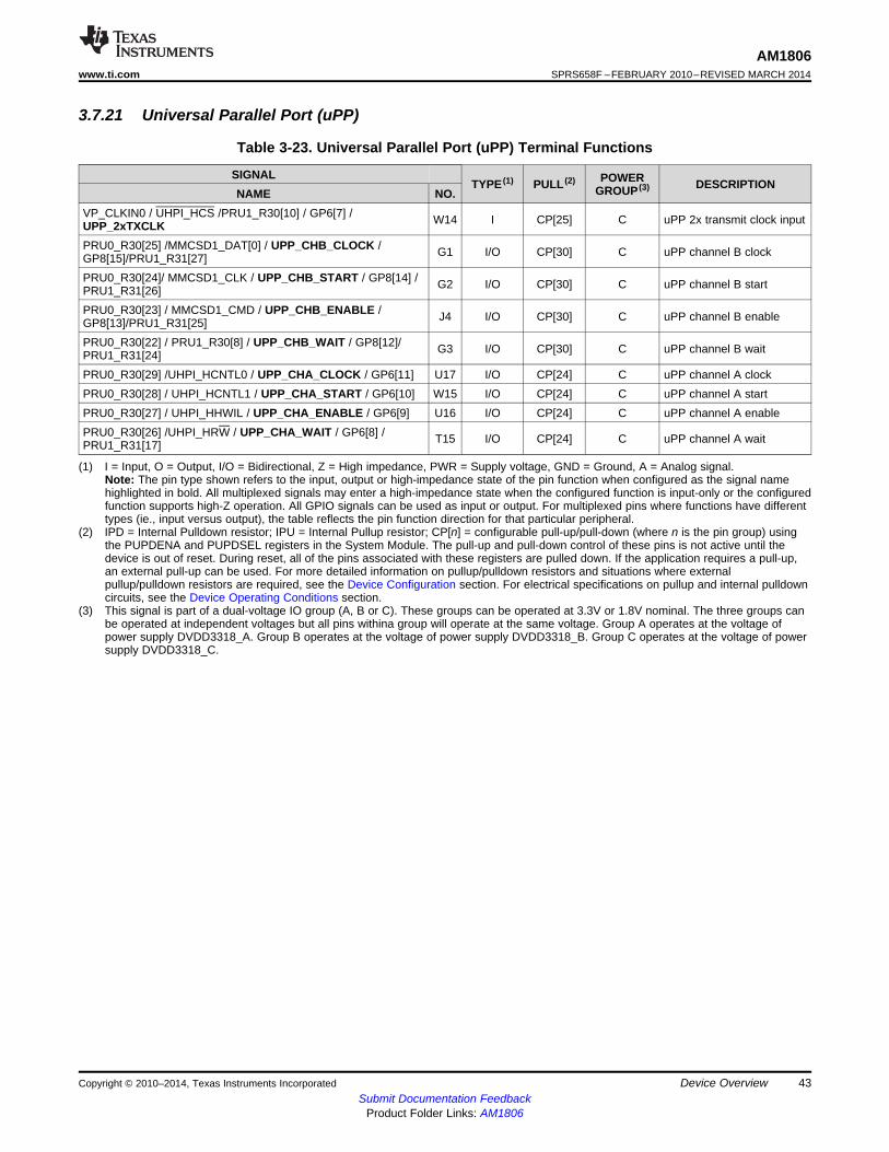
AM1806www.ti.com SPRS658F –FEBRUARY 2010–REVISED MARCH 2014
3.7.21 Universal Parallel Port (uPP)
Table 3-23. Universal Parallel Port (uPP) Terminal Functions
SIGNAL POWERTYPE (1) PULL (2) DESCRIPTIONGROUP (3)NAME NO.VP_CLKIN0 / UHPI_HCS /PRU1_R30[10] / GP6[7] / W14 I CP[25] C uPP 2x transmit clock inputUPP_2xTXCLKPRU0_R30[25] /MMCSD1_DAT[0] / UPP_CHB_CLOCK / G1 I/O CP[30] C uPP channel B clockGP8[15]/PRU1_R31[27]PRU0_R30[24]/ MMCSD1_CLK / UPP_CHB_START / GP8[14] / G2 I/O CP[30] C uPP channel B startPRU1_R31[26]PRU0_R30[23] / MMCSD1_CMD / UPP_CHB_ENABLE / J4 I/O CP[30] C uPP channel B enableGP8[13]/PRU1_R31[25]PRU0_R30[22] / PRU1_R30[8] / UPP_CHB_WAIT / GP8[12]/ G3 I/O CP[30] C uPP channel B waitPRU1_R31[24]PRU0_R30[29] /UHPI_HCNTL0 / UPP_CHA_CLOCK / GP6[11] U17 I/O CP[24] C uPP channel A clockPRU0_R30[28] / UHPI_HCNTL1 / UPP_CHA_START / GP6[10] W15 I/O CP[24] C uPP channel A startPRU0_R30[27] / UHPI_HHWIL / UPP_CHA_ENABLE / GP6[9] U16 I/O CP[24] C uPP channel A enablePRU0_R30[26] /UHPI_HRW / UPP_CHA_WAIT / GP6[8] / T15 I/O CP[24] C uPP channel A waitPRU1_R31[17]
(1) I = Input, O = Output, I/O = Bidirectional, Z = High impedance, PWR = Supply voltage, GND = Ground, A = Analog signal.Note: The pin type shown refers to the input, output or high-impedance state of the pin function when configured as the signal namehighlighted in bold. All multiplexed signals may enter a high-impedance state when the configured function is input-only or the configuredfunction supports high-Z operation. All GPIO signals can be used as input or output. For multiplexed pins where functions have differenttypes (ie., input versus output), the table reflects the pin function direction for that particular peripheral.
(2) IPD = Internal Pulldown resistor; IPU = Internal Pullup resistor; CP[n] = configurable pull-up/pull-down (where n is the pin group) usingthe PUPDENA and PUPDSEL registers in the System Module. The pull-up and pull-down control of these pins is not active until thedevice is out of reset. During reset, all of the pins associated with these registers are pulled down. If the application requires a pull-up,an external pull-up can be used. For more detailed information on pullup/pulldown resistors and situations where externalpullup/pulldown resistors are required, see the Device Configuration section. For electrical specifications on pullup and internal pulldowncircuits, see the Device Operating Conditions section.
(3) This signal is part of a dual-voltage IO group (A, B or C). These groups can be operated at 3.3V or 1.8V nominal. The three groups canbe operated at independent voltages but all pins withina group will operate at the same voltage. Group A operates at the voltage ofpower supply DVDD3318_A. Group B operates at the voltage of power supply DVDD3318_B. Group C operates at the voltage of powersupply DVDD3318_C.
Copyright © 2010–2014, Texas Instruments Incorporated Device Overview 43Submit Documentation Feedback
Product Folder Links: AM1806
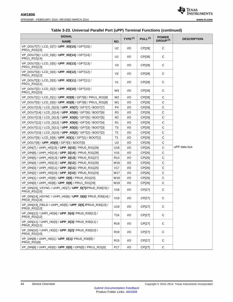
AM1806SPRS658F –FEBRUARY 2010–REVISED MARCH 2014 www.ti.com
Table 3-23. Universal Parallel Port (uPP) Terminal Functions (continued)SIGNAL POWERTYPE (1) PULL (2) DESCRIPTIONGROUP (3)NAME NO.
VP_DOUT[7] / LCD_D[7] / UPP_XD[15] / GP7[15] / U2 I/O CP[28] CPRU1_R31[15]VP_DOUT[6] / LCD_D[6] / UPP_XD[14] / GP7[14] / U1 I/O CP[28] CPRU1_R31[14]VP_DOUT[5] / LCD_D[5] / UPP_XD[13] / GP7[13] / V3 I/O CP[28] CPRU1_R31[13]VP_DOUT[4] / LCD_D[4] / UPP_XD[12] / GP7[12] / V2 I/O CP[28] CPRU1_R31[12]VP_DOUT[3] / LCD_D[3] / UPP_XD[11] / GP7[11] / V1 I/O CP[28] CPRU1_R31[11]VP_DOUT[2] / LCD_D[2] / UPP_XD[10] / GP7[10] / W3 I/O CP[28] CPRU1_R31[10]VP_DOUT[1] / LCD_D[1] / UPP_XD[9] / GP7[9] / PRU1_R31[9] W2 I/O CP[28] CVP_DOUT[0] / LCD_D[0] / UPP_XD[8] / GP7[8] / PRU1_R31[8] W1 I/O CP[28] CVP_DOUT[15] / LCD_D[15] / UPP_XD[7] / GP7[7] / BOOT[7] P4 I/O CP[29] CVP_DOUT[14] / LCD_D[14] / UPP_XD[6] / GP7[6] / BOOT[6] R3 I/O CP[29] CVP_DOUT[13] / LCD_D[13] / UPP_XD[5] / GP7[5] / BOOT[5] R2 I/O CP[29] CVP_DOUT[12] / LCD_D[12] / UPP_XD[4] / GP7[4] / BOOT[4] R1 I/O CP[29] CVP_DOUT[11] / LCD_D[11] / UPP_XD[3] / GP7[3] / BOOT[3] T3 I/O CP[29] CVP_DOUT[10] / LCD_D[10] / UPP_XD[2] / GP7[2] / BOOT[2] T2 I/O CP[29] CVP_DOUT[9] / LCD_D[9] / UPP_XD[1] / GP7[1] / BOOT[1] T1 I/O CP[29] CVP_DOUT[8] / UPP_XD[0] / GP7[0] / BOOT[0] U3 I/O CP[29] C
uPP data busVP_DIN[7] / UHPI_HD[15] / UPP_D[15] / PRU0_R31[29] U18 I/O CP[26] CVP_DIN[6] / UHPI_HD[14] / UPP_D[14] / PRU0_R31[28] V16 I/O CP[26] CVP_DIN[5] / UHPI_HD[13] / UPP_D[13] / PRU0_R31[27] R14 I/O CP[26] CVP_DIN[4] / UHPI_HD[12] / UPP_D[12] / PRU0_R31[26] W16 I/O CP[26] CVP_DIN[3] / UHPI_HD[11] / UPP_D[11] / PRU0_R31[25] V17 I/O CP[26] CVP_DIN[2] / UHPI_HD[10] / UPP_D[10] / PRU0_R31[24] W17 I/O CP[26] CVP_DIN[1] / UHPI_HD[9] / UPP_D[9] / PRU0_R31[23] W18 I/O CP[26] CVP_DIN[0] / UHPI_HD[8] / UPP_D[8] / PRU1_R31[29] W19 I/O CP[26] CVP_DIN[15]_VSYNC / UHPI_HD[7] / UPP_D[7]/PRU0_R30[15] / V18 I/O CP[27] CPRU0_R31[15]VP_DIN[14]_HSYNC / UHPI_HD[6] / UPP_D[6]/ PRU0_R30[14] / V19 I/O CP[27] CPRU0_R31[14]VP_DIN[13]_FIELD / UHPI_HD[5] / UPP_D[5] /PRU0_R30[13] / U19 I/O CP[27] CPRU0_R31[13]VP_DIN[12] / UHPI_HD[4] / UPP_D[4]/ PRU0_R30[12] / T16 I/O CP[27] CPRU0_R31[12]VP_DIN[11] / UHPI_HD[3] / UPP_D[3]/ PRU0_R30[11] / R18 I/O CP[27] CPRU0_R31[11]VP_DIN[10] / UHPI_HD[2] / UPP_D[2]/ PRU0_R30[10] / R19 I/O CP[27] CPRU0_R31[10]VP_DIN[9] / UHPI_HD[1] / UPP_D[1]/ PRU0_R30[9] / R15 I/O CP[27] CPRU0_R31[9]VP_DIN[8] / UHPI_HD[0] / UPP_D[0] / GP6[5] / PRU1_R31[0] P17 I/O CP[27] C
44 Device Overview Copyright © 2010–2014, Texas Instruments IncorporatedSubmit Documentation Feedback
Product Folder Links: AM1806
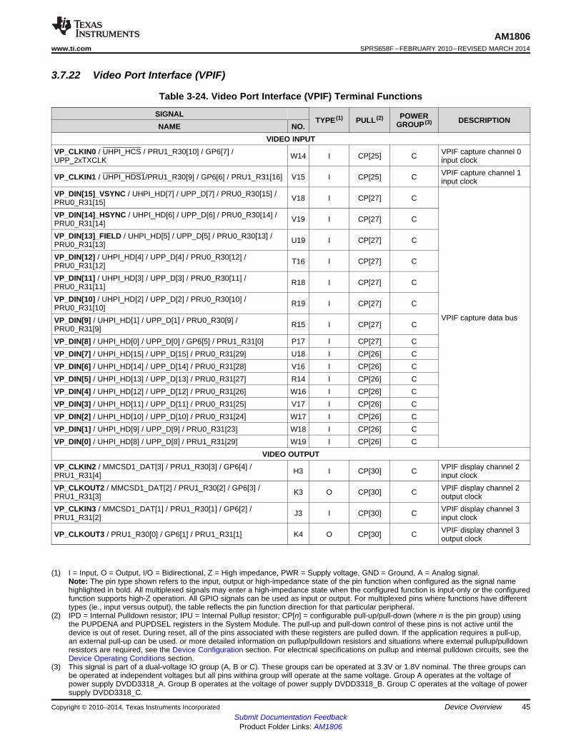
AM1806www.ti.com SPRS658F –FEBRUARY 2010–REVISED MARCH 2014
3.7.22 Video Port Interface (VPIF)
Table 3-24. Video Port Interface (VPIF) Terminal Functions
SIGNAL POWERTYPE (1) PULL (2) DESCRIPTIONGROUP (3)NAME NO.VIDEO INPUT
VP_CLKIN0 / UHPI_HCS / PRU1_R30[10] / GP6[7] / VPIF capture channel 0W14 I CP[25] CUPP_2xTXCLK input clockVPIF capture channel 1VP_CLKIN1 / UHPI_HDS1/PRU1_R30[9] / GP6[6] / PRU1_R31[16] V15 I CP[25] C input clock
VP_DIN[15]_VSYNC / UHPI_HD[7] / UPP_D[7] / PRU0_R30[15] / V18 I CP[27] CPRU0_R31[15]VP_DIN[14]_HSYNC / UHPI_HD[6] / UPP_D[6] / PRU0_R30[14] / V19 I CP[27] CPRU0_R31[14]VP_DIN[13]_FIELD / UHPI_HD[5] / UPP_D[5] / PRU0_R30[13] / U19 I CP[27] CPRU0_R31[13]VP_DIN[12] / UHPI_HD[4] / UPP_D[4] / PRU0_R30[12] / T16 I CP[27] CPRU0_R31[12]VP_DIN[11] / UHPI_HD[3] / UPP_D[3] / PRU0_R30[11] / R18 I CP[27] CPRU0_R31[11]VP_DIN[10] / UHPI_HD[2] / UPP_D[2] / PRU0_R30[10] / R19 I CP[27] CPRU0_R31[10]
VPIF capture data busVP_DIN[9] / UHPI_HD[1] / UPP_D[1] / PRU0_R30[9] / R15 I CP[27] CPRU0_R31[9]VP_DIN[8] / UHPI_HD[0] / UPP_D[0] / GP6[5] / PRU1_R31[0] P17 I CP[27] CVP_DIN[7] / UHPI_HD[15] / UPP_D[15] / PRU0_R31[29] U18 I CP[26] CVP_DIN[6] / UHPI_HD[14] / UPP_D[14] / PRU0_R31[28] V16 I CP[26] CVP_DIN[5] / UHPI_HD[13] / UPP_D[13] / PRU0_R31[27] R14 I CP[26] CVP_DIN[4] / UHPI_HD[12] / UPP_D[12] / PRU0_R31[26] W16 I CP[26] CVP_DIN[3] / UHPI_HD[11] / UPP_D[11] / PRU0_R31[25] V17 I CP[26] CVP_DIN[2] / UHPI_HD[10] / UPP_D[10] / PRU0_R31[24] W17 I CP[26] CVP_DIN[1] / UHPI_HD[9] / UPP_D[9] / PRU0_R31[23] W18 I CP[26] CVP_DIN[0] / UHPI_HD[8] / UPP_D[8] / PRU1_R31[29] W19 I CP[26] C
VIDEO OUTPUTVP_CLKIN2 / MMCSD1_DAT[3] / PRU1_R30[3] / GP6[4] / VPIF display channel 2H3 I CP[30] CPRU1_R31[4] input clockVP_CLKOUT2 / MMCSD1_DAT[2] / PRU1_R30[2] / GP6[3] / VPIF display channel 2K3 O CP[30] CPRU1_R31[3] output clockVP_CLKIN3 / MMCSD1_DAT[1] / PRU1_R30[1] / GP6[2] / VPIF display channel 3J3 I CP[30] CPRU1_R31[2] input clock
VPIF display channel 3VP_CLKOUT3 / PRU1_R30[0] / GP6[1] / PRU1_R31[1] K4 O CP[30] C output clock
(1) I = Input, O = Output, I/O = Bidirectional, Z = High impedance, PWR = Supply voltage, GND = Ground, A = Analog signal.Note: The pin type shown refers to the input, output or high-impedance state of the pin function when configured as the signal namehighlighted in bold. All multiplexed signals may enter a high-impedance state when the configured function is input-only or the configuredfunction supports high-Z operation. All GPIO signals can be used as input or output. For multiplexed pins where functions have differenttypes (ie., input versus output), the table reflects the pin function direction for that particular peripheral.
(2) IPD = Internal Pulldown resistor; IPU = Internal Pullup resistor; CP[n] = configurable pull-up/pull-down (where n is the pin group) usingthe PUPDENA and PUPDSEL registers in the System Module. The pull-up and pull-down control of these pins is not active until thedevice is out of reset. During reset, all of the pins associated with these registers are pulled down. If the application requires a pull-up,an external pull-up can be used. or more detailed information on pullup/pulldown resistors and situations where external pullup/pulldownresistors are required, see the Device Configuration section. For electrical specifications on pullup and internal pulldown circuits, see theDevice Operating Conditions section.
(3) This signal is part of a dual-voltage IO group (A, B or C). These groups can be operated at 3.3V or 1.8V nominal. The three groups canbe operated at independent voltages but all pins withina group will operate at the same voltage. Group A operates at the voltage ofpower supply DVDD3318_A. Group B operates at the voltage of power supply DVDD3318_B. Group C operates at the voltage of powersupply DVDD3318_C.
Copyright © 2010–2014, Texas Instruments Incorporated Device Overview 45Submit Documentation Feedback
Product Folder Links: AM1806
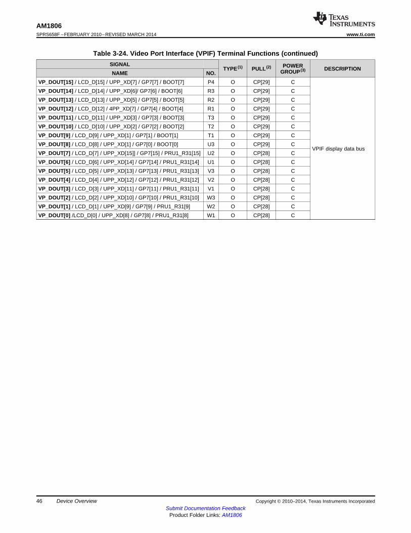
AM1806SPRS658F –FEBRUARY 2010–REVISED MARCH 2014 www.ti.com
Table 3-24. Video Port Interface (VPIF) Terminal Functions (continued)SIGNAL POWERTYPE (1) PULL (2) DESCRIPTIONGROUP (3)NAME NO.
VP_DOUT[15] / LCD_D[15] / UPP_XD[7] / GP7[7] / BOOT[7] P4 O CP[29] CVP_DOUT[14] / LCD_D[14] / UPP_XD[6]/ GP7[6] / BOOT[6] R3 O CP[29] CVP_DOUT[13] / LCD_D[13] / UPP_XD[5] / GP7[5] / BOOT[5] R2 O CP[29] CVP_DOUT[12] / LCD_D[12] / 4PP_XD[7] / GP7[4] / BOOT[4] R1 O CP[29] CVP_DOUT[11] / LCD_D[11] / UPP_XD[3] / GP7[3] / BOOT[3] T3 O CP[29] CVP_DOUT[10] / LCD_D[10] / UPP_XD[2] / GP7[2] / BOOT[2] T2 O CP[29] CVP_DOUT[9] / LCD_D[9] / UPP_XD[1] / GP7[1] / BOOT[1] T1 O CP[29] CVP_DOUT[8] / LCD_D[8] / UPP_XD[1] / GP7[0] / BOOT[0] U3 O CP[29] C
VPIF display data busVP_DOUT[7] / LCD_D[7] / UPP_XD[15]] / GP7[15] / PRU1_R31[15] U2 O CP[28] CVP_DOUT[6] / LCD_D[6] / UPP_XD[14] / GP7[14] / PRU1_R31[14] U1 O CP[28] CVP_DOUT[5] / LCD_D[5] / UPP_XD[13] / GP7[13] / PRU1_R31[13] V3 O CP[28] CVP_DOUT[4] / LCD_D[4] / UPP_XD[12] / GP7[12] / PRU1_R31[12] V2 O CP[28] CVP_DOUT[3] / LCD_D[3] / UPP_XD[11] / GP7[11] / PRU1_R31[11] V1 O CP[28] CVP_DOUT[2] / LCD_D[2] / UPP_XD[10] / GP7[10] / PRU1_R31[10] W3 O CP[28] CVP_DOUT[1] / LCD_D[1] / UPP_XD[9] / GP7[9] / PRU1_R31[9] W2 O CP[28] CVP_DOUT[0] /LCD_D[0] / UPP_XD[8] / GP7[8] / PRU1_R31[8] W1 O CP[28] C
46 Device Overview Copyright © 2010–2014, Texas Instruments IncorporatedSubmit Documentation Feedback
Product Folder Links: AM1806
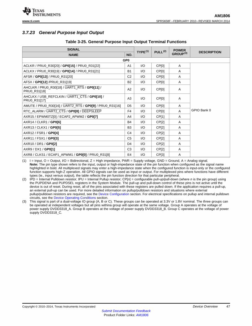
AM1806www.ti.com SPRS658F –FEBRUARY 2010–REVISED MARCH 2014
3.7.23 General Purpose Input Output
Table 3-25. General Purpose Input Output Terminal Functions
SIGNAL POWERTYPE (1) PULL (2) DESCRIPTIONGROUP (3)NAME NO.GP0
ACLKR / PRU0_R30[20] / GP0[15] / PRU0_R31[22] A1 I/O CP[0] AACLKX / PRU0_R30[19] / GP0[14] / PRU0_R31[21] B1 I/O CP[0] AAFSR / GP0[13] / PRU0_R31[20] C2 I/O CP[0] AAFSX / GP0[12] /PRU0_R31[19] B2 I/O CP[0] AAHCLKR / PRU0_R30[18] / UART1_RTS / GP0[11] / A2 I/O CP[0] APRU0_R31[18]AHCLKX / USB_REFCLKIN / UART1_CTS / GP0[10] / A3 I/O CP[0] APRU0_R31[17]AMUTE / PRU0_R30[16] / UART2_RTS / GP0[9] / PRU0_R31[16] D5 I/O CP[0] A
GPIO Bank 0RTC_ALARM / UART2_CTS / GP0[8] / DEEPSLEEP F4 I/O CP[0] AAXR15 / EPWM0TZ[0] / ECAP2_APWM2 / GP0[7] A4 I/O CP[1] AAXR14 / CLKR1 / GP0[6] B4 I/O CP[2] AAXR13 / CLKX1 / GP0[5] B3 I/O CP[2] AAXR12 / FSR1 / GP0[4] C4 I/O CP[2] AAXR11 / FSX1 / GP0[3] C5 I/O CP[2] AAXR10 / DR1 / GP0[2] D4 I/O CP[2] AAXR9 / DX1 / GP0[1] C3 I/O CP[2] AAXR8 / CLKS1 / ECAP1_APWM1 / GP0[0] / PRU0_R31[8] E4 I/O CP[3] A
(1) I = Input, O = Output, I/O = Bidirectional, Z = High impedance, PWR = Supply voltage, GND = Ground, A = Analog signal.Note: The pin type shown refers to the input, output or high-impedance state of the pin function when configured as the signal namehighlighted in bold. All multiplexed signals may enter a high-impedance state when the configured function is input-only or the configuredfunction supports high-Z operation. All GPIO signals can be used as input or output. For multiplexed pins where functions have differenttypes (ie., input versus output), the table reflects the pin function direction for that particular peripheral.
(2) IPD = Internal Pulldown resistor; IPU = Internal Pullup resistor; CP[n] = configurable pull-up/pull-down (where n is the pin group) usingthe PUPDENA and PUPDSEL registers in the System Module. The pull-up and pull-down control of these pins is not active until thedevice is out of reset. During reset, all of the pins associated with these registers are pulled down. If the application requires a pull-up,an external pull-up can be used. For more detailed information on pullup/pulldown resistors and situations where externalpullup/pulldown resistors are required, see the Device Configuration section. For electrical specifications on pullup and internal pulldowncircuits, see the Device Operating Conditions section.
(3) This signal is part of a dual-voltage IO group (A, B or C). These groups can be operated at 3.3V or 1.8V nominal. The three groups canbe operated at independent voltages but all pins withina group will operate at the same voltage. Group A operates at the voltage ofpower supply DVDD3318_A. Group B operates at the voltage of power supply DVDD3318_B. Group C operates at the voltage of powersupply DVDD3318_C.
Copyright © 2010–2014, Texas Instruments Incorporated Device Overview 47Submit Documentation Feedback
Product Folder Links: AM1806
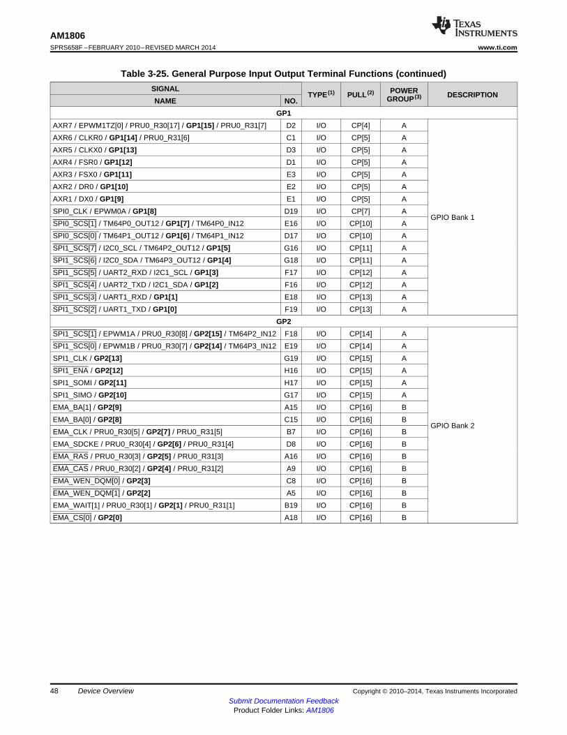
AM1806SPRS658F –FEBRUARY 2010–REVISED MARCH 2014 www.ti.com
Table 3-25. General Purpose Input Output Terminal Functions (continued)SIGNAL POWERTYPE (1) PULL (2) DESCRIPTIONGROUP (3)NAME NO.
GP1AXR7 / EPWM1TZ[0] / PRU0_R30[17] / GP1[15] / PRU0_R31[7] D2 I/O CP[4] AAXR6 / CLKR0 / GP1[14] / PRU0_R31[6] C1 I/O CP[5] AAXR5 / CLKX0 / GP1[13] D3 I/O CP[5] AAXR4 / FSR0 / GP1[12] D1 I/O CP[5] AAXR3 / FSX0 / GP1[11] E3 I/O CP[5] AAXR2 / DR0 / GP1[10] E2 I/O CP[5] AAXR1 / DX0 / GP1[9] E1 I/O CP[5] ASPI0_CLK / EPWM0A / GP1[8] D19 I/O CP[7] A
GPIO Bank 1SPI0_SCS[1] / TM64P0_OUT12 / GP1[7] / TM64P0_IN12 E16 I/O CP[10] ASPI0_SCS[0] / TM64P1_OUT12 / GP1[6] / TM64P1_IN12 D17 I/O CP[10] ASPI1_SCS[7] / I2C0_SCL / TM64P2_OUT12 / GP1[5] G16 I/O CP[11] ASPI1_SCS[6] / I2C0_SDA / TM64P3_OUT12 / GP1[4] G18 I/O CP[11] ASPI1_SCS[5] / UART2_RXD / I2C1_SCL / GP1[3] F17 I/O CP[12] ASPI1_SCS[4] / UART2_TXD / I2C1_SDA / GP1[2] F16 I/O CP[12] ASPI1_SCS[3] / UART1_RXD / GP1[1] E18 I/O CP[13] ASPI1_SCS[2] / UART1_TXD / GP1[0] F19 I/O CP[13] A
GP2SPI1_SCS[1] / EPWM1A / PRU0_R30[8] / GP2[15] / TM64P2_IN12 F18 I/O CP[14] ASPI1_SCS[0] / EPWM1B / PRU0_R30[7] / GP2[14] / TM64P3_IN12 E19 I/O CP[14] ASPI1_CLK / GP2[13] G19 I/O CP[15] ASPI1_ENA / GP2[12] H16 I/O CP[15] ASPI1_SOMI / GP2[11] H17 I/O CP[15] ASPI1_SIMO / GP2[10] G17 I/O CP[15] AEMA_BA[1] / GP2[9] A15 I/O CP[16] BEMA_BA[0] / GP2[8] C15 I/O CP[16] B
GPIO Bank 2EMA_CLK / PRU0_R30[5] / GP2[7] / PRU0_R31[5] B7 I/O CP[16] BEMA_SDCKE / PRU0_R30[4] / GP2[6] / PRU0_R31[4] D8 I/O CP[16] BEMA_RAS / PRU0_R30[3] / GP2[5] / PRU0_R31[3] A16 I/O CP[16] BEMA_CAS / PRU0_R30[2] / GP2[4] / PRU0_R31[2] A9 I/O CP[16] BEMA_WEN_DQM[0] / GP2[3] C8 I/O CP[16] BEMA_WEN_DQM[1] / GP2[2] A5 I/O CP[16] BEMA_WAIT[1] / PRU0_R30[1] / GP2[1] / PRU0_R31[1] B19 I/O CP[16] BEMA_CS[0] / GP2[0] A18 I/O CP[16] B
48 Device Overview Copyright © 2010–2014, Texas Instruments IncorporatedSubmit Documentation Feedback
Product Folder Links: AM1806
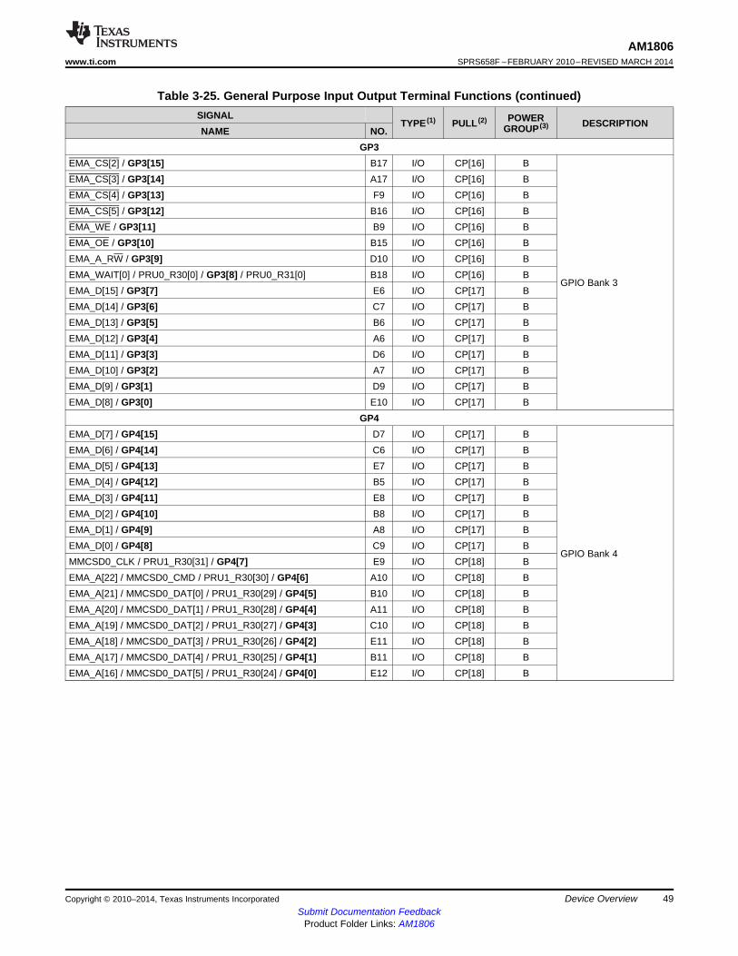
AM1806www.ti.com SPRS658F –FEBRUARY 2010–REVISED MARCH 2014
Table 3-25. General Purpose Input Output Terminal Functions (continued)SIGNAL POWERTYPE (1) PULL (2) DESCRIPTIONGROUP (3)NAME NO.
GP3EMA_CS[2] / GP3[15] B17 I/O CP[16] BEMA_CS[3] / GP3[14] A17 I/O CP[16] BEMA_CS[4] / GP3[13] F9 I/O CP[16] BEMA_CS[5] / GP3[12] B16 I/O CP[16] BEMA_WE / GP3[11] B9 I/O CP[16] BEMA_OE / GP3[10] B15 I/O CP[16] BEMA_A_RW / GP3[9] D10 I/O CP[16] BEMA_WAIT[0] / PRU0_R30[0] / GP3[8] / PRU0_R31[0] B18 I/O CP[16] B
GPIO Bank 3EMA_D[15] / GP3[7] E6 I/O CP[17] BEMA_D[14] / GP3[6] C7 I/O CP[17] BEMA_D[13] / GP3[5] B6 I/O CP[17] BEMA_D[12] / GP3[4] A6 I/O CP[17] BEMA_D[11] / GP3[3] D6 I/O CP[17] BEMA_D[10] / GP3[2] A7 I/O CP[17] BEMA_D[9] / GP3[1] D9 I/O CP[17] BEMA_D[8] / GP3[0] E10 I/O CP[17] B
GP4EMA_D[7] / GP4[15] D7 I/O CP[17] BEMA_D[6] / GP4[14] C6 I/O CP[17] BEMA_D[5] / GP4[13] E7 I/O CP[17] BEMA_D[4] / GP4[12] B5 I/O CP[17] BEMA_D[3] / GP4[11] E8 I/O CP[17] BEMA_D[2] / GP4[10] B8 I/O CP[17] BEMA_D[1] / GP4[9] A8 I/O CP[17] BEMA_D[0] / GP4[8] C9 I/O CP[17] B
GPIO Bank 4MMCSD0_CLK / PRU1_R30[31] / GP4[7] E9 I/O CP[18] BEMA_A[22] / MMCSD0_CMD / PRU1_R30[30] / GP4[6] A10 I/O CP[18] BEMA_A[21] / MMCSD0_DAT[0] / PRU1_R30[29] / GP4[5] B10 I/O CP[18] BEMA_A[20] / MMCSD0_DAT[1] / PRU1_R30[28] / GP4[4] A11 I/O CP[18] BEMA_A[19] / MMCSD0_DAT[2] / PRU1_R30[27] / GP4[3] C10 I/O CP[18] BEMA_A[18] / MMCSD0_DAT[3] / PRU1_R30[26] / GP4[2] E11 I/O CP[18] BEMA_A[17] / MMCSD0_DAT[4] / PRU1_R30[25] / GP4[1] B11 I/O CP[18] BEMA_A[16] / MMCSD0_DAT[5] / PRU1_R30[24] / GP4[0] E12 I/O CP[18] B
Copyright © 2010–2014, Texas Instruments Incorporated Device Overview 49Submit Documentation Feedback
Product Folder Links: AM1806
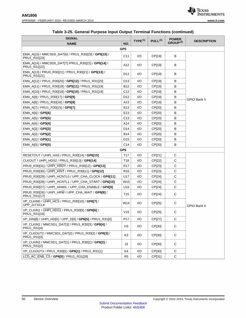
AM1806SPRS658F –FEBRUARY 2010–REVISED MARCH 2014 www.ti.com
Table 3-25. General Purpose Input Output Terminal Functions (continued)SIGNAL POWERTYPE (1) PULL (2) DESCRIPTIONGROUP (3)NAME NO.
GP5EMA_A[15] / MMCSD0_DAT[6] / PRU1_R30[23] / GP5[15] / C11 I/O CP[19] BPRU1_R31[23]EMA_A[14] / MMCSD0_DAT[7] /PRU1_R30[22] / GP5[14] / A12 I/O CP[19] BPRU1_R31[22]EMA_A[13] / PRU0_R30[21] / PRU1_R30[21] / GP5[13] / D11 I/O CP[19] BPRU1_R31[21]EMA_A[12] / PRU1_R30[20] / GP5[12] / PRU1_R31[20] D13 I/O CP[19] BEMA_A[11] / PRU1_R30[19] / GP5[11] / PRU1_R31[19] B12 I/O CP[19] BEMA_A[10] / PRU1_R30[18] / GP5[10] / PRU1_R31[18] C12 I/O CP[19] BEMA_A[9] / PRU1_R30[17] / GP5[9] D12 I/O CP[19] B
GPIO Bank 5EMA_A[8] / PRU1_R30[16] / GP5[8] A13 I/O CP[19] BEMA_A[7] / PRU1_R30[15] / GP5[7] B13 I/O CP[20] BEMA_A[6] / GP5[6] E13 I/O CP[20] BEMA_A[5] / GP5[5] C13 I/O CP[20] BEMA_A[4] / GP5[4] A14 I/O CP[20] BEMA_A[3] / GP5[3] D14 I/O CP[20] BEMA_A[2] / GP5[2] B14 I/O CP[20] BEMA_A[1] / GP5[1] D15 I/O CP[20] BEMA_A[0] / GP5[0] C14 I/O CP[20] B
GP6RESETOUT / UHPI_HAS / PRU1_R30[14] / GP6[15] T17 I/O CP[21] CCLKOUT / UHPI_HDS2 / PRU1_R30[13] / GP6[14] T18 I/O CP[22] CPRU0_R30[31] / UHPI_HRDY / PRU1_R30[12] / GP6[13] R17 I/O CP[23] CPRU0_R30[30] / UHPI_HINT / PRU1_R30[11] / GP6[12] R16 I/O CP[23] CPRU0_R30[29] / UHPI_HCNTL0 / UPP_CHA_CLOCK / GP6[11] U17 I/O CP[24] CPRU0_R30[28] / UHPI_HCNTL1 / UPP_CHA_START / GP6[10] W15 I/O CP[24] CPRU0_R30[27] / UHPI_HHWIL / UPP_CHA_ENABLE / GP6[9] U16 I/O CP[24] CPRU0_R30[26] / UHPI_HRW / UPP_CHA_WAIT / GP6[8] / T15 I/O CP[24] CPRU1_R31[17]VP_CLKIN0 / UHPI_HCS / PRU1_R30[10] / GP6[7] / W14 I/O CP[25] CUPP_2xTXCLK GPIO Bank 6VP_CLKIN1 / UHPI_HDS1 / PRU1_R30[9] / GP6[6] / V15 I/O CP[25] CPRU1_R31[16]VP_DIN[8] / UHPI_HD[0] / UPP_D[0] / GP6[5] / PRU1_R31[0] P17 I/O CP[27] CVP_CLKIN2 / MMCSD1_DAT[3] / PRU1_R30[3] / GP6[4] / H3 I/O CP[30] CPRU1_R31[4]VP_CLKOUT2 / MMCSD1_DAT[2] / PRU1_R30[2] / GP6[3] / K3 I/O CP[30] CPRU1_R31[3]VP_CLKIN3 / MMCSD1_DAT[1] / PRU1_R30[1] / GP6[2] / J3 I/O CP[30] CPRU1_R31[2]VP_CLKOUT3 / PRU1_R30[0] / GP6[1] / PRU1_R31[1] K4 I/O CP[30] CLCD_AC_ENB_CS / GP6[0] / PRU1_R31[28] R5 I/O CP[31] C
50 Device Overview Copyright © 2010–2014, Texas Instruments IncorporatedSubmit Documentation Feedback
Product Folder Links: AM1806
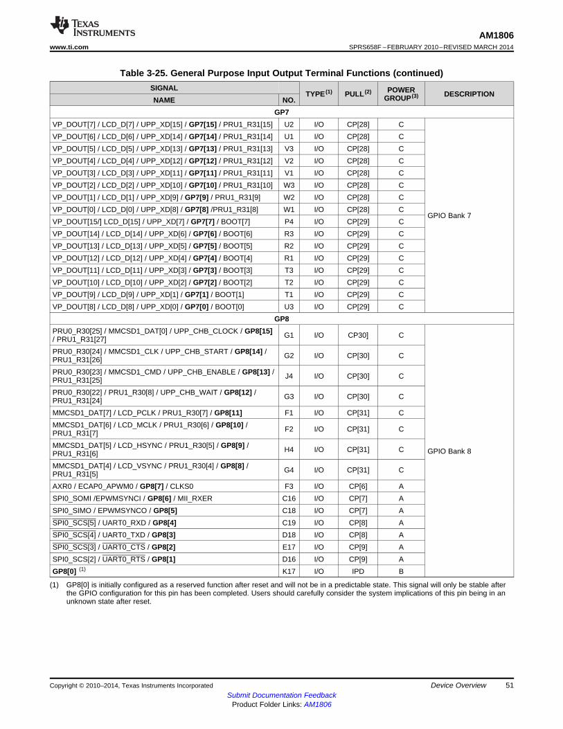
AM1806www.ti.com SPRS658F –FEBRUARY 2010–REVISED MARCH 2014
Table 3-25. General Purpose Input Output Terminal Functions (continued)SIGNAL POWERTYPE (1) PULL (2) DESCRIPTIONGROUP (3)NAME NO.
GP7VP_DOUT[7] / LCD_D[7] / UPP_XD[15] / GP7[15] / PRU1_R31[15] U2 I/O CP[28] CVP_DOUT[6] / LCD_D[6] / UPP_XD[14] / GP7[14] / PRU1_R31[14] U1 I/O CP[28] CVP_DOUT[5] / LCD_D[5] / UPP_XD[13] / GP7[13] / PRU1_R31[13] V3 I/O CP[28] CVP_DOUT[4] / LCD_D[4] / UPP_XD[12] / GP7[12] / PRU1_R31[12] V2 I/O CP[28] CVP_DOUT[3] / LCD_D[3] / UPP_XD[11] / GP7[11] / PRU1_R31[11] V1 I/O CP[28] CVP_DOUT[2] / LCD_D[2] / UPP_XD[10] / GP7[10] / PRU1_R31[10] W3 I/O CP[28] CVP_DOUT[1] / LCD_D[1] / UPP_XD[9] / GP7[9] / PRU1_R31[9] W2 I/O CP[28] CVP_DOUT[0] / LCD_D[0] / UPP_XD[8] / GP7[8] /PRU1_R31[8] W1 I/O CP[28] C
GPIO Bank 7VP_DOUT[15/] LCD_D[15] / UPP_XD[7] / GP7[7] / BOOT[7] P4 I/O CP[29] CVP_DOUT[14] / LCD_D[14] / UPP_XD[6] / GP7[6] / BOOT[6] R3 I/O CP[29] CVP_DOUT[13] / LCD_D[13] / UPP_XD[5] / GP7[5] / BOOT[5] R2 I/O CP[29] CVP_DOUT[12] / LCD_D[12] / UPP_XD[4] / GP7[4] / BOOT[4] R1 I/O CP[29] CVP_DOUT[11] / LCD_D[11] / UPP_XD[3] / GP7[3] / BOOT[3] T3 I/O CP[29] CVP_DOUT[10] / LCD_D[10] / UPP_XD[2] / GP7[2] / BOOT[2] T2 I/O CP[29] CVP_DOUT[9] / LCD_D[9] / UPP_XD[1] / GP7[1] / BOOT[1] T1 I/O CP[29] CVP_DOUT[8] / LCD_D[8] / UPP_XD[0] / GP7[0] / BOOT[0] U3 I/O CP[29] C
GP8PRU0_R30[25] / MMCSD1_DAT[0] / UPP_CHB_CLOCK / GP8[15] G1 I/O CP30] C/ PRU1_R31[27]PRU0_R30[24] / MMCSD1_CLK / UPP_CHB_START / GP8[14] / G2 I/O CP[30] CPRU1_R31[26]PRU0_R30[23] / MMCSD1_CMD / UPP_CHB_ENABLE / GP8[13] / J4 I/O CP[30] CPRU1_R31[25]PRU0_R30[22] / PRU1_R30[8] / UPP_CHB_WAIT / GP8[12] / G3 I/O CP[30] CPRU1_R31[24]MMCSD1_DAT[7] / LCD_PCLK / PRU1_R30[7] / GP8[11] F1 I/O CP[31] CMMCSD1_DAT[6] / LCD_MCLK / PRU1_R30[6] / GP8[10] / F2 I/O CP[31] CPRU1_R31[7]MMCSD1_DAT[5] / LCD_HSYNC / PRU1_R30[5] / GP8[9] / H4 I/O CP[31] C GPIO Bank 8PRU1_R31[6]MMCSD1_DAT[4] / LCD_VSYNC / PRU1_R30[4] / GP8[8] / G4 I/O CP[31] CPRU1_R31[5]AXR0 / ECAP0_APWM0 / GP8[7] / CLKS0 F3 I/O CP[6] ASPI0_SOMI /EPWMSYNCI / GP8[6] / MII_RXER C16 I/O CP[7] ASPI0_SIMO / EPWMSYNCO / GP8[5] C18 I/O CP[7] ASPI0_SCS[5] / UART0_RXD / GP8[4] C19 I/O CP[8] ASPI0_SCS[4] / UART0_TXD / GP8[3] D18 I/O CP[8] ASPI0_SCS[3] / UART0_CTS / GP8[2] E17 I/O CP[9] ASPI0_SCS[2] / UART0_RTS / GP8[1] D16 I/O CP[9] AGP8[0] (1) K17 I/O IPD B
(1) GP8[0] is initially configured as a reserved function after reset and will not be in a predictable state. This signal will only be stable afterthe GPIO configuration for this pin has been completed. Users should carefully consider the system implications of this pin being in anunknown state after reset.
Copyright © 2010–2014, Texas Instruments Incorporated Device Overview 51Submit Documentation Feedback
Product Folder Links: AM1806
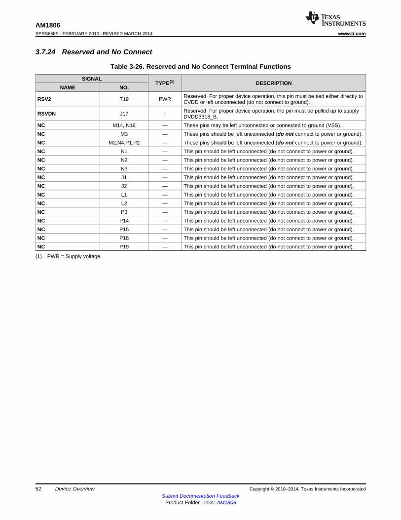
AM1806SPRS658F –FEBRUARY 2010–REVISED MARCH 2014 www.ti.com
3.7.24 Reserved and No Connect
Table 3-26. Reserved and No Connect Terminal Functions
SIGNALTYPE (1) DESCRIPTION
NAME NO.Reserved. For proper device operation, this pin must be tied either directly toRSV2 T19 PWR CVDD or left unconnected (do not connect to ground).Reserved. For proper device operation, the pin must be pulled up to supplyRSVDN J17 I DVDD3318_B.
NC M14, N16 — These pins may be left unconnected or connected to ground (VSS).NC M3 — These pins should be left unconnected (do not connect to power or ground).NC M2,N4,P1,P2 — These pins should be left unconnected (do not connect to power or ground).NC N1 — This pin should be left unconnected (do not connect to power or ground).NC N2 — This pin should be left unconnected (do not connect to power or ground).NC N3 — This pin should be left unconnected (do not connect to power or ground).NC J1 — This pin should be left unconnected (do not connect to power or ground).NC J2 — This pin should be left unconnected (do not connect to power or ground).NC L1 — This pin should be left unconnected (do not connect to power or ground).NC L2 — This pin should be left unconnected (do not connect to power or ground).NC P3 — This pin should be left unconnected (do not connect to power or ground).NC P14 — This pin should be left unconnected (do not connect to power or ground).NC P15 — This pin should be left unconnected (do not connect to power or ground).NC P18 — This pin should be left unconnected (do not connect to power or ground).NC P19 — This pin should be left unconnected (do not connect to power or ground).
(1) PWR = Supply voltage.
52 Device Overview Copyright © 2010–2014, Texas Instruments IncorporatedSubmit Documentation Feedback
Product Folder Links: AM1806
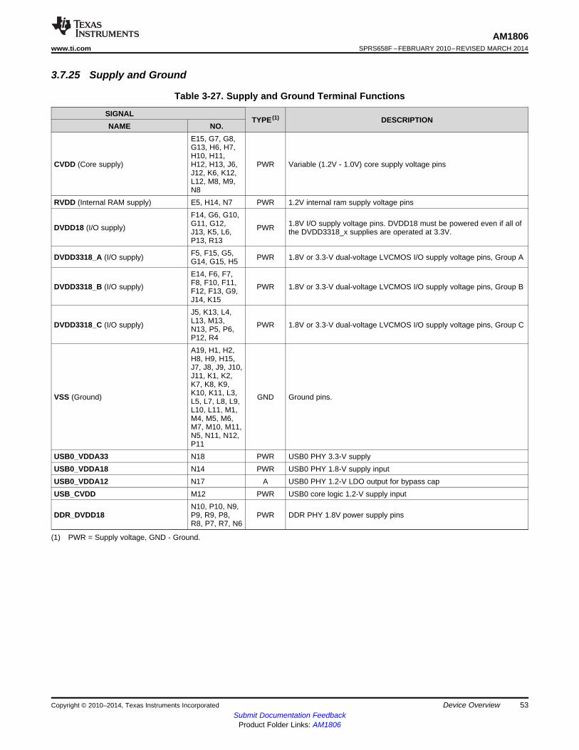
AM1806www.ti.com SPRS658F –FEBRUARY 2010–REVISED MARCH 2014
3.7.25 Supply and Ground
Table 3-27. Supply and Ground Terminal Functions
SIGNALTYPE (1) DESCRIPTION
NAME NO.E15, G7, G8,G13, H6, H7,H10, H11,
CVDD (Core supply) H12, H13, J6, PWR Variable (1.2V - 1.0V) core supply voltage pinsJ12, K6, K12,L12, M8, M9,N8
RVDD (Internal RAM supply) E5, H14, N7 PWR 1.2V internal ram supply voltage pinsF14, G6, G10,G11, G12, 1.8V I/O supply voltage pins. DVDD18 must be powered even if all ofDVDD18 (I/O supply) PWRJ13, K5, L6, the DVDD3318_x supplies are operated at 3.3V.P13, R13F5, F15, G5,DVDD3318_A (I/O supply) PWR 1.8V or 3.3-V dual-voltage LVCMOS I/O supply voltage pins, Group AG14, G15, H5E14, F6, F7,F8, F10, F11,DVDD3318_B (I/O supply) PWR 1.8V or 3.3-V dual-voltage LVCMOS I/O supply voltage pins, Group BF12, F13, G9,J14, K15J5, K13, L4,L13, M13,DVDD3318_C (I/O supply) PWR 1.8V or 3.3-V dual-voltage LVCMOS I/O supply voltage pins, Group CN13, P5, P6,P12, R4A19, H1, H2,H8, H9, H15,J7, J8, J9, J10,J11, K1, K2,K7, K8, K9,K10, K11, L3,VSS (Ground) GND Ground pins.L5, L7, L8, L9,L10, L11, M1,M4, M5, M6,M7, M10, M11,N5, N11, N12,P11
USB0_VDDA33 N18 PWR USB0 PHY 3.3-V supplyUSB0_VDDA18 N14 PWR USB0 PHY 1.8-V supply inputUSB0_VDDA12 N17 A USB0 PHY 1.2-V LDO output for bypass capUSB_CVDD M12 PWR USB0 core logic 1.2-V supply input
N10, P10, N9,DDR_DVDD18 P9, R9, P8, PWR DDR PHY 1.8V power supply pins
R8, P7, R7, N6
(1) PWR = Supply voltage, GND - Ground.
Copyright © 2010–2014, Texas Instruments Incorporated Device Overview 53Submit Documentation Feedback
Product Folder Links: AM1806
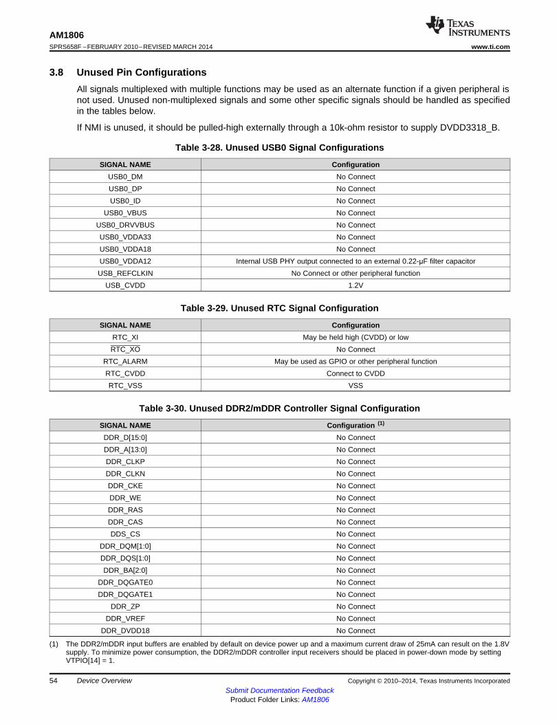
AM1806SPRS658F –FEBRUARY 2010–REVISED MARCH 2014 www.ti.com
3.8 Unused Pin ConfigurationsAll signals multiplexed with multiple functions may be used as an alternate function if a given peripheral isnot used. Unused non-multiplexed signals and some other specific signals should be handled as specifiedin the tables below.
If NMI is unused, it should be pulled-high externally through a 10k-ohm resistor to supply DVDD3318_B.
Table 3-28. Unused USB0 Signal Configurations
SIGNAL NAME ConfigurationUSB0_DM No ConnectUSB0_DP No ConnectUSB0_ID No Connect
USB0_VBUS No ConnectUSB0_DRVVBUS No ConnectUSB0_VDDA33 No ConnectUSB0_VDDA18 No ConnectUSB0_VDDA12 Internal USB PHY output connected to an external 0.22-μF filter capacitorUSB_REFCLKIN No Connect or other peripheral function
USB_CVDD 1.2V
Table 3-29. Unused RTC Signal Configuration
SIGNAL NAME ConfigurationRTC_XI May be held high (CVDD) or lowRTC_XO No Connect
RTC_ALARM May be used as GPIO or other peripheral functionRTC_CVDD Connect to CVDDRTC_VSS VSS
Table 3-30. Unused DDR2/mDDR Controller Signal Configuration
SIGNAL NAME Configuration (1)
DDR_D[15:0] No ConnectDDR_A[13:0] No ConnectDDR_CLKP No ConnectDDR_CLKN No ConnectDDR_CKE No ConnectDDR_WE No ConnectDDR_RAS No ConnectDDR_CAS No ConnectDDS_CS No Connect
DDR_DQM[1:0] No ConnectDDR_DQS[1:0] No ConnectDDR_BA[2:0] No Connect
DDR_DQGATE0 No ConnectDDR_DQGATE1 No Connect
DDR_ZP No ConnectDDR_VREF No Connect
DDR_DVDD18 No Connect
(1) The DDR2/mDDR input buffers are enabled by default on device power up and a maximum current draw of 25mA can result on the 1.8Vsupply. To minimize power consumption, the DDR2/mDDR controller input receivers should be placed in power-down mode by settingVTPIO[14] = 1.
54 Device Overview Copyright © 2010–2014, Texas Instruments IncorporatedSubmit Documentation Feedback
Product Folder Links: AM1806

AM1806www.ti.com SPRS658F –FEBRUARY 2010–REVISED MARCH 2014
4 Device Configuration
4.1 Boot ModesThis device supports a variety of boot modes through an internal ARM ROM bootloader. This device doesnot support dedicated hardware boot modes. The input states of the BOOT pins are sampled and latchedinto the BOOTCFG register, which is part of the system configuration (SYSCFG) module, when devicereset is deasserted. Boot mode selection is determined by the values of the BOOT pins.
See Using the OMAP-L1x8 Bootloader Application Report (SPRAB41) for more details on the ROM BootLoader.
The following boot modes are supported:• NAND Flash boot
– 8-bit NAND– 16-bit NAND (supported on ROM revisions after d800k002 -- see the bootloader documents
mentioned above to determine the ROM revision)• NOR Flash boot
– NOR Direct boot (8-bit or 16-bit)– NOR Legacy boot (8-bit or 16-bit)– NOR AIS boot (8-bit or 16-bit)
• HPI Boot• I2C0/I2C1 Boot
– EEPROM (Master Mode)– External Host (Slave Mode)
• SPI0/SPI1 Boot– Serial Flash (Master Mode)– SERIAL EEPROM (Master Mode)– External Host (Slave Mode)
• UART0/UART1/UART2 Boot– External Host
• MMC/SD0 Boot
4.2 SYSCFG ModuleThe following system level features of the chip are controlled by the SYSCFG peripheral:• Readable Device, Die, and Chip Revision ID• Control of Pin Multiplexing• Priority of bus accesses different bus masters in the system• Capture at power on reset the chip BOOT pin values and make them available to software• Control of the DeepSleep power management function• Enable and selection of the programmable pin pullups and pulldowns• Special case settings for peripherals:
– Locking of PLL controller settings– Default burst sizes for EDMA3 transfer controllers– Selection of the source for the eCAP module input capture (including on chip sources)– McASP AMUTEIN selection and clearing of AMUTE status for the McASP– Control of the reference clock source and other side-band signals for both of the integrated USB
PHYs– Clock source selection for EMIFA– DDR2 Controller PHY settings
Copyright © 2010–2014, Texas Instruments Incorporated Device Configuration 55Submit Documentation Feedback
Product Folder Links: AM1806
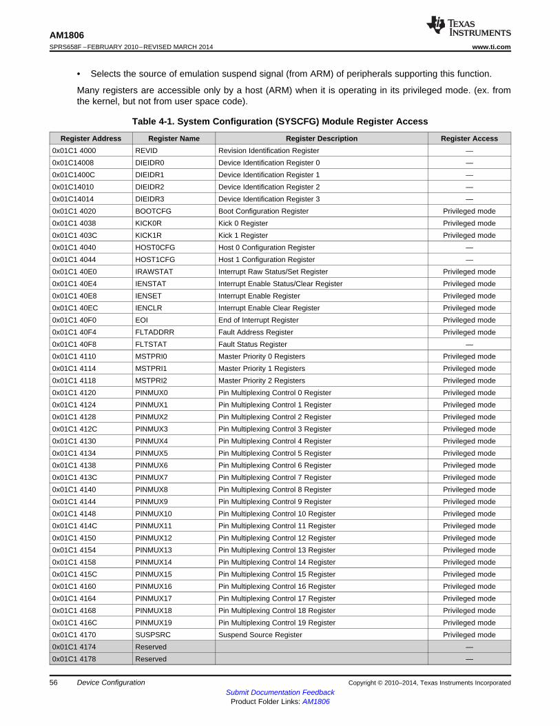
AM1806SPRS658F –FEBRUARY 2010–REVISED MARCH 2014 www.ti.com
• Selects the source of emulation suspend signal (from ARM) of peripherals supporting this function.
Many registers are accessible only by a host (ARM) when it is operating in its privileged mode. (ex. fromthe kernel, but not from user space code).
Table 4-1. System Configuration (SYSCFG) Module Register Access
Register Address Register Name Register Description Register Access0x01C1 4000 REVID Revision Identification Register —0x01C14008 DIEIDR0 Device Identification Register 0 —0x01C1400C DIEIDR1 Device Identification Register 1 —0x01C14010 DIEIDR2 Device Identification Register 2 —0x01C14014 DIEIDR3 Device Identification Register 3 —0x01C1 4020 BOOTCFG Boot Configuration Register Privileged mode0x01C1 4038 KICK0R Kick 0 Register Privileged mode0x01C1 403C KICK1R Kick 1 Register Privileged mode0x01C1 4040 HOST0CFG Host 0 Configuration Register —0x01C1 4044 HOST1CFG Host 1 Configuration Register —0x01C1 40E0 IRAWSTAT Interrupt Raw Status/Set Register Privileged mode0x01C1 40E4 IENSTAT Interrupt Enable Status/Clear Register Privileged mode0x01C1 40E8 IENSET Interrupt Enable Register Privileged mode0x01C1 40EC IENCLR Interrupt Enable Clear Register Privileged mode0x01C1 40F0 EOI End of Interrupt Register Privileged mode0x01C1 40F4 FLTADDRR Fault Address Register Privileged mode0x01C1 40F8 FLTSTAT Fault Status Register —0x01C1 4110 MSTPRI0 Master Priority 0 Registers Privileged mode0x01C1 4114 MSTPRI1 Master Priority 1 Registers Privileged mode0x01C1 4118 MSTPRI2 Master Priority 2 Registers Privileged mode0x01C1 4120 PINMUX0 Pin Multiplexing Control 0 Register Privileged mode0x01C1 4124 PINMUX1 Pin Multiplexing Control 1 Register Privileged mode0x01C1 4128 PINMUX2 Pin Multiplexing Control 2 Register Privileged mode0x01C1 412C PINMUX3 Pin Multiplexing Control 3 Register Privileged mode0x01C1 4130 PINMUX4 Pin Multiplexing Control 4 Register Privileged mode0x01C1 4134 PINMUX5 Pin Multiplexing Control 5 Register Privileged mode0x01C1 4138 PINMUX6 Pin Multiplexing Control 6 Register Privileged mode0x01C1 413C PINMUX7 Pin Multiplexing Control 7 Register Privileged mode0x01C1 4140 PINMUX8 Pin Multiplexing Control 8 Register Privileged mode0x01C1 4144 PINMUX9 Pin Multiplexing Control 9 Register Privileged mode0x01C1 4148 PINMUX10 Pin Multiplexing Control 10 Register Privileged mode0x01C1 414C PINMUX11 Pin Multiplexing Control 11 Register Privileged mode0x01C1 4150 PINMUX12 Pin Multiplexing Control 12 Register Privileged mode0x01C1 4154 PINMUX13 Pin Multiplexing Control 13 Register Privileged mode0x01C1 4158 PINMUX14 Pin Multiplexing Control 14 Register Privileged mode0x01C1 415C PINMUX15 Pin Multiplexing Control 15 Register Privileged mode0x01C1 4160 PINMUX16 Pin Multiplexing Control 16 Register Privileged mode0x01C1 4164 PINMUX17 Pin Multiplexing Control 17 Register Privileged mode0x01C1 4168 PINMUX18 Pin Multiplexing Control 18 Register Privileged mode0x01C1 416C PINMUX19 Pin Multiplexing Control 19 Register Privileged mode0x01C1 4170 SUSPSRC Suspend Source Register Privileged mode0x01C1 4174 Reserved —0x01C1 4178 Reserved —
56 Device Configuration Copyright © 2010–2014, Texas Instruments IncorporatedSubmit Documentation Feedback
Product Folder Links: AM1806
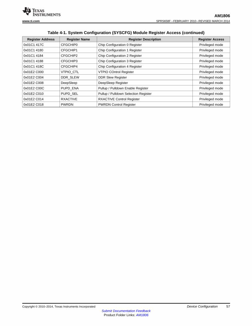
AM1806www.ti.com SPRS658F –FEBRUARY 2010–REVISED MARCH 2014
Table 4-1. System Configuration (SYSCFG) Module Register Access (continued)Register Address Register Name Register Description Register Access
0x01C1 417C CFGCHIP0 Chip Configuration 0 Register Privileged mode0x01C1 4180 CFGCHIP1 Chip Configuration 1 Register Privileged mode0x01C1 4184 CFGCHIP2 Chip Configuration 2 Register Privileged mode0x01C1 4188 CFGCHIP3 Chip Configuration 3 Register Privileged mode0x01C1 418C CFGCHIP4 Chip Configuration 4 Register Privileged mode0x01E2 C000 VTPIO_CTL VTPIO COntrol Register Privileged mode0x01E2 C004 DDR_SLEW DDR Slew Register Privileged mode0x01E2 C008 DeepSleep DeepSleep Register Privileged mode0x01E2 C00C PUPD_ENA Pullup / Pulldown Enable Register Privileged mode0x01E2 C010 PUPD_SEL Pullup / Pulldown Selection Register Privileged mode0x01E2 C014 RXACTIVE RXACTIVE Control Register Privileged mode0x01E2 C018 PWRDN PWRDN Control Register Privileged mode
Copyright © 2010–2014, Texas Instruments Incorporated Device Configuration 57Submit Documentation Feedback
Product Folder Links: AM1806

AM1806SPRS658F –FEBRUARY 2010–REVISED MARCH 2014 www.ti.com
4.3 Pullup/Pulldown ResistorsProper board design should ensure that input pins to the device always be at a valid logic level and notfloating. This may be achieved via pullup/pulldown resistors. The device features internal pullup (IPU) andinternal pulldown (IPD) resistors on most pins to eliminate the need, unless otherwise noted, for externalpullup/pulldown resistors.
An external pullup/pulldown resistor needs to be used in the following situations:• Boot and Configuration Pins: If the pin is both routed out and 3-stated (not driven), an external
pullup/pulldown resistor is strongly recommended, even if the IPU/IPD matches the desired value/state.• Other Input Pins: If the IPU/IPD does not match the desired value/state, use an external
pullup/pulldown resistor to pull the signal to the opposite rail.
For the boot and configuration pins, if they are both routed out and 3-stated (not driven), it is stronglyrecommended that an external pullup/pulldown resistor be implemented. Although, internalpullup/pulldown resistors exist on these pins and they may match the desired configuration value,providing external connectivity can help ensure that valid logic levels are latched on these device boot andconfiguration pins. In addition, applying external pullup/pulldown resistors on the boot and configurationpins adds convenience to the user in debugging and flexibility in switching operating modes.
Tips for choosing an external pullup/pulldown resistor:• Consider the total amount of current that may pass through the pullup or pulldown resistor. Make sure
to include the leakage currents of all the devices connected to the net, as well as any internal pullup orpulldown resistors.
• Decide a target value for the net. For a pulldown resistor, this should be below the lowest VIL level ofall inputs connected to the net. For a pullup resistor, this should be above the highest VIH level of allinputs on the net. A reasonable choice would be to target the VOL or VOH levels for the logic family ofthe limiting device; which, by definition, have margin to the VIL and VIH levels.
• Select a pullup/pulldown resistor with the largest possible value; but, which can still ensure that the netwill reach the target pulled value when maximum current from all devices on the net is flowing throughthe resistor. The current to be considered includes leakage current plus, any other internal andexternal pullup/pulldown resistors on the net.
• For bidirectional nets, there is an additional consideration which sets a lower limit on the resistancevalue of the external resistor. Verify that the resistance is small enough that the weakest output buffercan drive the net to the opposite logic level (including margin).
• Remember to include tolerances when selecting the resistor value.• For pullup resistors, also remember to include tolerances on the IO supply rail.• For most systems, a 1-kΩ resistor can be used to oppose the IPU/IPD while meeting the above
criteria. Users should confirm this resistor value is correct for their specific application.• For most systems, a 20-kΩ resistor can be used to compliment the IPU/IPD on the boot and
configuration pins while meeting the above criteria. Users should confirm this resistor value is correctfor their specific application.
• For more detailed information on input current (II), and the low-/high-level input voltages (VIL and VIH)for the device, see Section 5.3, Recommended Operating Conditions.
• For the internal pullup/pulldown resistors for all device pins, see the peripheral/system-specific terminalfunctions table.
58 Device Configuration Copyright © 2010–2014, Texas Instruments IncorporatedSubmit Documentation Feedback
Product Folder Links: AM1806
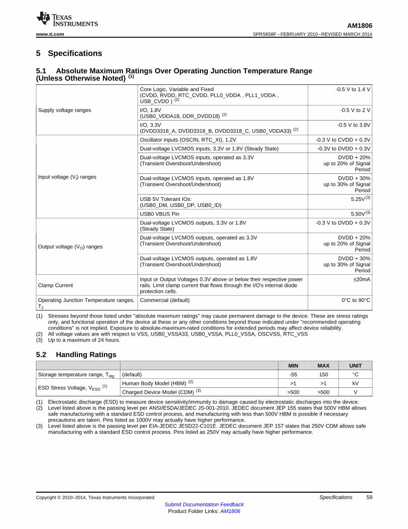
AM1806www.ti.com SPRS658F –FEBRUARY 2010–REVISED MARCH 2014
5 Specifications
5.1 Absolute Maximum Ratings Over Operating Junction Temperature Range(Unless Otherwise Noted) (1)
Core Logic, Variable and Fixed -0.5 V to 1.4 V(CVDD, RVDD, RTC_CVDD, PLL0_VDDA , PLL1_VDDA ,USB_CVDD ) (2)
Supply voltage ranges I/O, 1.8V -0.5 V to 2 V(USB0_VDDA18, DDR_DVDD18) (2)
I/O, 3.3V -0.5 V to 3.8V(DVDD3318_A, DVDD3318_B, DVDD3318_C, USB0_VDDA33) (2)
Oscillator inputs (OSCIN, RTC_XI), 1.2V -0.3 V to CVDD + 0.3VDual-voltage LVCMOS inputs, 3.3V or 1.8V (Steady State) -0.3V to DVDD + 0.3VDual-voltage LVCMOS inputs, operated as 3.3V DVDD + 20%(Transient Overshoot/Undershoot) up to 20% of Signal
PeriodInput voltage (VI) ranges Dual-voltage LVCMOS inputs, operated as 1.8V DVDD + 30%
(Transient Overshoot/Undershoot) up to 30% of SignalPeriod
USB 5V Tolerant IOs: 5.25V (3)
(USB0_DM, USB0_DP, USB0_ID)USB0 VBUS Pin 5.50V (3)
Dual-voltage LVCMOS outputs, 3.3V or 1.8V -0.3 V to DVDD + 0.3V(Steady State)Dual-voltage LVCMOS outputs, operated as 3.3V DVDD + 20%(Transient Overshoot/Undershoot) up to 20% of SignalOutput voltage (VO) ranges PeriodDual-voltage LVCMOS outputs, operated as 1.8V DVDD + 30%(Transient Overshoot/Undershoot) up to 30% of Signal
PeriodInput or Output Voltages 0.3V above or below their respective power ±20mA
Clamp Current rails. Limit clamp current that flows through the I/O's internal diodeprotection cells.
Operating Junction Temperature ranges, Commercial (default) 0°C to 90°CTJ
(1) Stresses beyond those listed under "absolute maximum ratings" may cause permanent damage to the device. These are stress ratingsonly, and functional operation of the device at these or any other conditions beyond those indicated under "recommended operatingconditions" is not implied. Exposure to absolute-maximum-rated conditions for extended periods may affect device reliability.
(2) All voltage values are with respect to VSS, USB0_VSSA33, USB0_VSSA, PLL0_VSSA, OSCVSS, RTC_VSS(3) Up to a maximum of 24 hours.
5.2 Handling RatingsMIN MAX UNIT
Storage temperature range, Tstg (default) -55 150 °CHuman Body Model (HBM) (2) >1 >1 kV
ESD Stress Voltage, VESD(1)
Charged Device Model (CDM) (3) >500 >500 V
(1) Electrostatic discharge (ESD) to measure device sensitivity/immunity to damage caused by electrostatic discharges into the device.(2) Level listed above is the passing level per ANSI/ESDA/JEDEC JS-001-2010. JEDEC document JEP 155 states that 500V HBM allows
safe manufacturing with a standard ESD control process, and manufacturing with less than 500V HBM is possible if necessaryprecautions are taken. Pins listed as 1000V may actually have higher performance.
(3) Level listed above is the passing level per EIA-JEDEC JESD22-C101E. JEDEC document JEP 157 states that 250V CDM allows safemanufacturing with a standard ESD control process. Pins listed as 250V may actually have higher performance.
Copyright © 2010–2014, Texas Instruments Incorporated Specifications 59Submit Documentation Feedback
Product Folder Links: AM1806
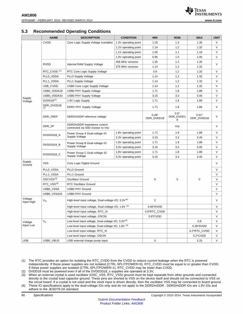
AM1806SPRS658F –FEBRUARY 2010–REVISED MARCH 2014 www.ti.com
5.3 Recommended Operating ConditionsNAME DESCRIPTION CONDITION MIN NOM MAX UNIT
CVDD Core Logic Supply Voltage (variable) 1.3V operating point 1.25 1.3 1.35 V
1.2V operating point 1.14 1.2 1.32 V
1.1V operating point 1.05 1.1 1.16 V
1.0V operating point 0.95 1.0 1.05 V
456 MHz versions 1.25 1.3 1.35RVDD Internal RAM Supply Voltage V
375 MHz versions 1.14 1.2 1.32
RTC_CVDD (1) RTC Core Logic Supply Voltage 0.9 1.2 1.32 V
PLL0_VDDA PLL0 Supply Voltage 1.14 1.2 1.32 V
PLL1_VDDA PLL1 Supply Voltage 1.14 1.2 1.32 V
USB_CVDD USB0 Core Logic Supply Voltage 1.14 1.2 1.32 V
USB0_VDDA18 USB0 PHY Supply Voltage 1.71 1.8 1.89 V
USB0_VDDA33 USB0 PHY Supply Voltage 3.15 3.3 3.45 VSupply
DVDD18 (2) 1.8V Logic Supply 1.71 1.8 1.89 VVoltageDDR_DVDD18 DDR2 PHY Supply Voltage 1.71 1.8 1.89 V(2)
0.5*0.49* 0.51*DDR_VREF DDR2/mDDR reference voltage DDR_DVDD1 VDDR_DVDD18 DDR_DVDD188
DDR2/mDDR impedance control,DDR_ZP Vss Vconnected via 50Ω resistor to Vss
1.8V operating point 1.71 1.8 1.89 VPower Group A Dual-voltage IODVDD3318_A Supply Voltage 3.3V operating point 3.15 3.3 3.45 V
1.8V operating point 1.71 1.8 1.89 VPower Group B Dual-voltage IODVDD3318_B Supply Voltage 3.3V operating point 3.15 3.3 3.45 V
1.8V operating point 1.71 1.8 1.89 VPower Group C Dual-voltage IODVDD3318_C Supply Voltage 3.3V operating point 3.15 3.3 3.45 V
Supply VSS Core Logic Digital Ground VGround
PLL0_VSSA PLL0 Ground V
PLL1_VSSA PLL1 Ground V
OSCVSS (3) Oscillator Ground 0 0 0 V
RTC_VSS (3) RTC Oscillator Ground V
USB0_VSSA USB0 PHY Ground V
USB0_VSSA33 USB0 PHY Ground V
Voltage VIH High-level input voltage, Dual-voltage I/O, 3.3V (4) 2 VInput High
High-level input voltage, Dual-voltage I/O, 1.8V (4) 0.65*DVDD V
High-level input voltage, RTC_XI 0.8*RTC_CVDD V
High-level input voltage, OSCIN 0.8*CVDD V
VIL Low-level input voltage, Dual-voltage I/O, 3.3V (4) 0.8 VVoltageInput Low Low-level input voltage, Dual-voltage I/O, 1.8V (4) 0.35*DVDD V
Low-level input voltage, RTC_XI 0.2*RTC_CVDD V
Low-level input voltage, OSCIN 0.2*CVDD V
USB USB0_VBUS USB external charge pump input 0 5.25 V
(1) The RTC provides an option for isolating the RTC_CVDD from the CVDD to reduce current leakage when the RTC is poweredindependently. If these power supplies are not isolated (CTRL.SPLITPOWER=0), RTC_CVDD must be equal to or greater than CVDD.If these power supplies are isolated (CTRL.SPLITPOWER=1), RTC_CVDD may be lower than CVDD.
(2) DVDD18 must be powered even if all of the DVDD3318_x supplies are operated at 3.3V.(3) When an external crystal is used oscillator (OSC_VSS, RTC_VSS) ground must be kept separate from other grounds and connected
directly to the crystal load capacitor ground. These pins are shorted to VSS on the device itself and should not be connected to VSS onthe circuit board. If a crystal is not used and the clock input is driven directly, then the oscillator VSS may be connected to board ground.
(4) These IO specifications apply to the dual-voltage IOs only and do not apply to the DDR2/mDDR . DDR2/mDDR IOs are 1.8V IOs andadhere to the JESD79-2A standard.
60 Specifications Copyright © 2010–2014, Texas Instruments IncorporatedSubmit Documentation Feedback
Product Folder Links: AM1806
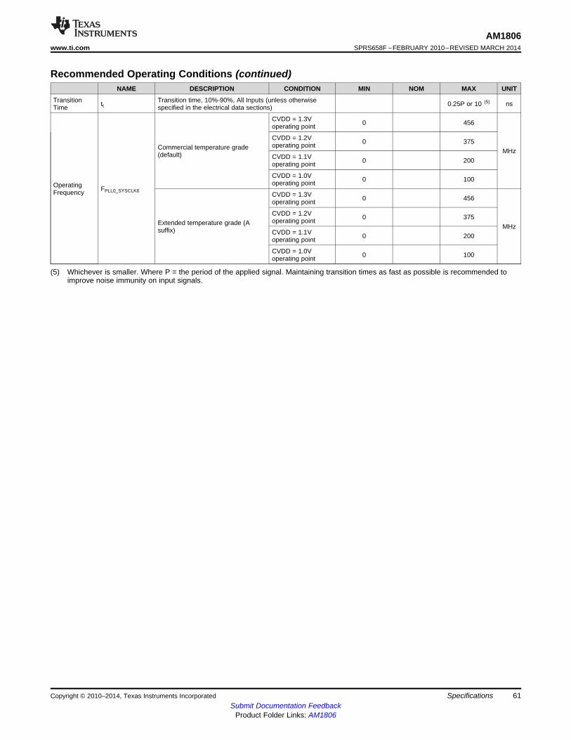
AM1806www.ti.com SPRS658F –FEBRUARY 2010–REVISED MARCH 2014
Recommended Operating Conditions (continued)NAME DESCRIPTION CONDITION MIN NOM MAX UNIT
Transition Transition time, 10%-90%, All Inputs (unless otherwisett 0.25P or 10 (5) nsTime specified in the electrical data sections)
CVDD = 1.3V 0 456operating point
CVDD = 1.2V 0 375operating pointCommercial temperature grade MHz(default) CVDD = 1.1V 0 200operating point
CVDD = 1.0V 0 100operating pointOperating FPLL0_SYSCLK6Frequency CVDD = 1.3V 0 456operating point
CVDD = 1.2V 0 375operating pointExtended temperature grade (A MHzsuffix) CVDD = 1.1V 0 200operating point
CVDD = 1.0V 0 100operating point
(5) Whichever is smaller. Where P = the period of the applied signal. Maintaining transition times as fast as possible is recommended toimprove noise immunity on input signals.
Copyright © 2010–2014, Texas Instruments Incorporated Specifications 61Submit Documentation Feedback
Product Folder Links: AM1806

AM1806SPRS658F –FEBRUARY 2010–REVISED MARCH 2014 www.ti.com
5.4 Notes on Recommended Power-On Hours (POH)The information in the section below is provided solely for your convenience and does not extend ormodify the warranty provided under TI’s standard terms and conditions for TI semiconductor products.
To avoid significant degradation, the device power-on hours (POH) must be limited to the following:
Table 5-1. Recommended Power-On Hours
Silicon Operating Junction Power-On Hours [POH]Speed Grade Nominal CVDD Voltage (V)Revision Temperature (Tj) (hours)B/E 300 MHz 0 to 90 °C 1.2V 100,000B/E 375 MHz 0 to 90 °C 1.2V 100,000B/E 375 MHz -40 to 105 °C 1.2V 75,000 (1)
B/E 456 MHz 0 to 90 °C 1.3V 100,000B/E 456 MHz -40 to 90 °C 1.3V 100,000
(1) 100,000 POH can be achieved at this temperature condition if the device operation is limited to 345 MHz
Note: Logic functions and parameter values are not assured out of the range specified in the recommendedoperating conditions.
The above notations cannot be deemed a warranty or deemed to extend or modify the warranty underTI’s standard terms and conditions for TI semiconductor products.
62 Specifications Copyright © 2010–2014, Texas Instruments IncorporatedSubmit Documentation Feedback
Product Folder Links: AM1806
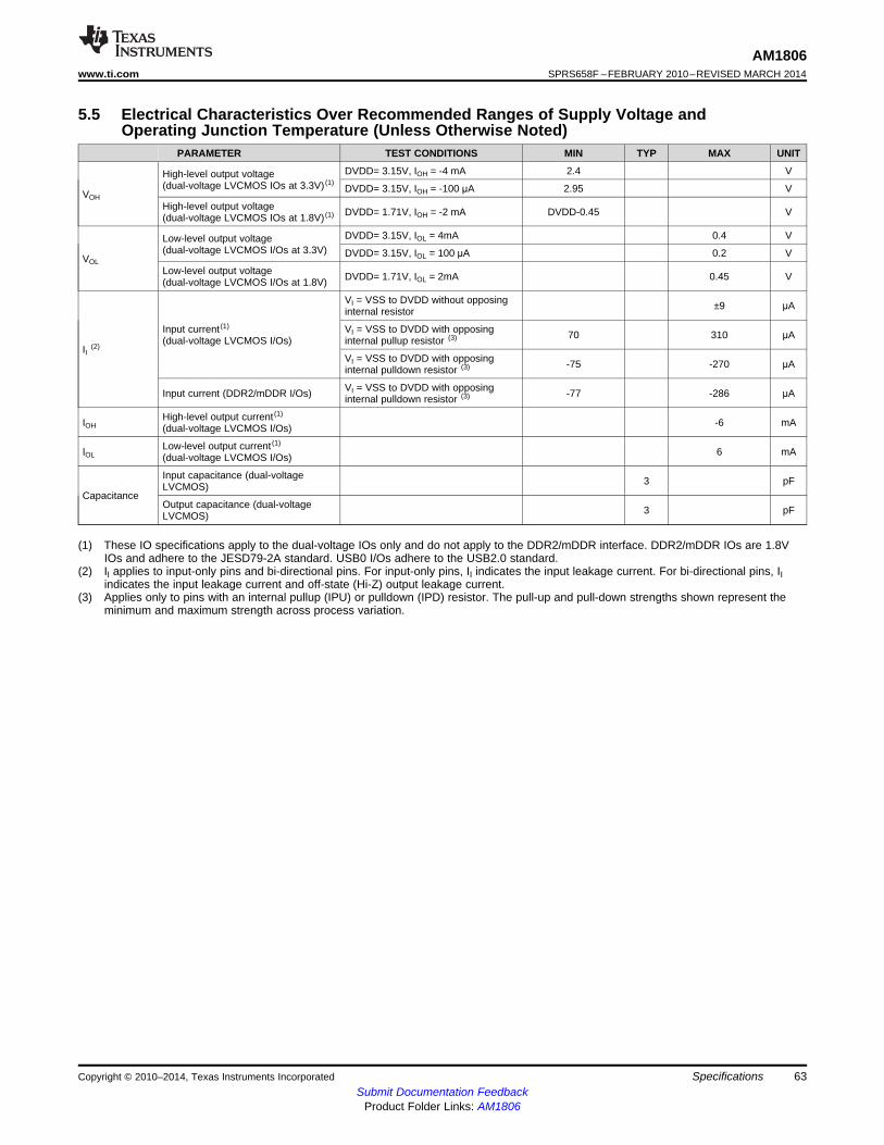
AM1806www.ti.com SPRS658F –FEBRUARY 2010–REVISED MARCH 2014
5.5 Electrical Characteristics Over Recommended Ranges of Supply Voltage andOperating Junction Temperature (Unless Otherwise Noted)
PARAMETER TEST CONDITIONS MIN TYP MAX UNIT
DVDD= 3.15V, IOH = -4 mA 2.4 VHigh-level output voltage(dual-voltage LVCMOS IOs at 3.3V) (1)
DVDD= 3.15V, IOH = -100 μA 2.95 VVOHHigh-level output voltage DVDD= 1.71V, IOH = -2 mA DVDD-0.45 V(dual-voltage LVCMOS IOs at 1.8V) (1)
DVDD= 3.15V, IOL = 4mA 0.4 VLow-level output voltage(dual-voltage LVCMOS I/Os at 3.3V) DVDD= 3.15V, IOL = 100 μA 0.2 VVOLLow-level output voltage DVDD= 1.71V, IOL = 2mA 0.45 V(dual-voltage LVCMOS I/Os at 1.8V)
VI = VSS to DVDD without opposing ±9 μAinternal resistor
Input current (1) VI = VSS to DVDD with opposing 70 310 μA(dual-voltage LVCMOS I/Os) internal pullup resistor (3)
II (2)
VI = VSS to DVDD with opposing -75 -270 μAinternal pulldown resistor (3)
VI = VSS to DVDD with opposingInput current (DDR2/mDDR I/Os) -77 -286 μAinternal pulldown resistor (3)
High-level output current (1)IOH -6 mA(dual-voltage LVCMOS I/Os)
Low-level output current (1)IOL 6 mA(dual-voltage LVCMOS I/Os)
Input capacitance (dual-voltage 3 pFLVCMOS)Capacitance
Output capacitance (dual-voltage 3 pFLVCMOS)
(1) These IO specifications apply to the dual-voltage IOs only and do not apply to the DDR2/mDDR interface. DDR2/mDDR IOs are 1.8VIOs and adhere to the JESD79-2A standard. USB0 I/Os adhere to the USB2.0 standard.
(2) II applies to input-only pins and bi-directional pins. For input-only pins, II indicates the input leakage current. For bi-directional pins, IIindicates the input leakage current and off-state (Hi-Z) output leakage current.
(3) Applies only to pins with an internal pullup (IPU) or pulldown (IPD) resistor. The pull-up and pull-down strengths shown represent theminimum and maximum strength across process variation.
Copyright © 2010–2014, Texas Instruments Incorporated Specifications 63Submit Documentation Feedback
Product Folder Links: AM1806
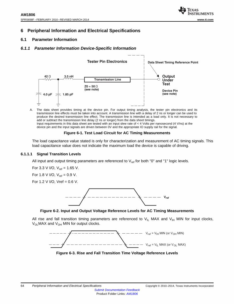
Vref = VIL MAX (or VOL MAX)
Vref = VIH MIN (or VOH MIN)
Vref
Transmission Line
4.0 pF 1.85 pF
Z0 = 50 Ω
(see note)
Tester Pin Electronics Data Sheet Timing Reference Point
OutputUnderTest
42 Ω 3.5 nH
Device Pin(see note)
AM1806SPRS658F –FEBRUARY 2010–REVISED MARCH 2014 www.ti.com
6 Peripheral Information and Electrical Specifications
6.1 Parameter Information
6.1.1 Parameter Information Device-Specific Information
A. The data sheet provides timing at the device pin. For output timing analysis, the tester pin electronics and itstransmission line effects must be taken into account. A transmission line with a delay of 2 ns or longer can be used toproduce the desired transmission line effect. The transmission line is intended as a load only. It is not necessary toadd or subtract the transmission line delay (2 ns or longer) from the data sheet timings.Input requirements in this data sheet are tested with an input slew rate of < 4 Volts per nanosecond (4 V/ns) at thedevice pin and the input signals are driven between 0V and the appropriate IO supply rail for the signal.
Figure 6-1. Test Load Circuit for AC Timing Measurements
The load capacitance value stated is only for characterization and measurement of AC timing signals. Thisload capacitance value does not indicate the maximum load the device is capable of driving.
6.1.1.1 Signal Transition Levels
All input and output timing parameters are referenced to Vref for both "0" and "1" logic levels.
For 3.3 V I/O, Vref = 1.65 V.
For 1.8 V I/O, Vref = 0.9 V.
For 1.2 V I/O, Vref = 0.6 V.
Figure 6-2. Input and Output Voltage Reference Levels for AC Timing Measurements
All rise and fall transition timing parameters are referenced to VIL MAX and VIH MIN for input clocks,VOLMAX and VOH MIN for output clocks.
Figure 6-3. Rise and Fall Transition Time Voltage Reference Levels
64 Peripheral Information and Electrical Specifications Copyright © 2010–2014, Texas Instruments IncorporatedSubmit Documentation Feedback
Product Folder Links: AM1806
AM1806www.ti.com SPRS658F –FEBRUARY 2010–REVISED MARCH 2014
6.2 Recommended Clock and Control Signal Transition BehaviorAll clocks and control signals must transition between VIH and VIL (or between VIL and VIH) in a monotonicmanner.
6.3 Power Supplies
6.3.1 Power-On SequenceThe device should be powered-on in the following order:1. RTC (RTC_CVDD) may be powered from an external device (such as a battery) prior to all other
supplies being applied or powered-up at the same time as CVDD. If the RTC is not used, RTC_CVDDshould be connected to CVDD. RTC_CVDD should not be left unpowered while CVDD is powered.
2. Core logic supplies:(a) All variable 1.2V - 1.0V core logic supplies (CVDD)(b) All static core logic supplies (RVDD, PLL0_VDDA, PLL1_VDDA, USB_CVDD). If voltage scaling is
not used on the device, groups 2a) and 2b) can be controlled from the same power supply andpowered up together.
3. All static 1.8V IO supplies (DVDD18, DDR_DVDD18, USB0_VDDA18 ) and any of the LVCMOS IOsupply groups used at 1.8V nominal (DVDD3318_A, DVDD3318_B, or DVDD3318_C).
4. All analog 3.3V PHY supplies (USB0_VDDA33; this is not required if USB0 is not used) and any of theLVCMOS IO supply groups used at 3.3V nominal (DVDD3318_A, DVDD3318_B, or DVDD3318_C).
There is no specific required voltage ramp rate for any of the supplies as long as the LVCMOS suppliesoperated at 3.3V (DVDD3318_A, DVDD3318_B, or DVDD3318_C) never exceed the STATIC 1.8Vsupplies by more than 2 volts.
RESET must be maintained active until all power supplies have reached their nominal values.
6.3.2 Power-Off SequenceThe power supplies can be powered-off in any order as long as LVCMOS supplies operated at 3.3V(DVDD3318_A, DVDD3318_B, or DVDD3318_C) never exceed static 1.8V supplies by more than 2 volts.There is no specific required voltage ramp down rate for any of the supplies (except as required to meetthe above mentioned voltage condition).
Copyright © 2010–2014, Texas Instruments Incorporated Peripheral Information and Electrical Specifications 65Submit Documentation Feedback
Product Folder Links: AM1806
AM1806SPRS658F –FEBRUARY 2010–REVISED MARCH 2014 www.ti.com
6.4 Reset
6.4.1 Power-On Reset (POR)A power-on reset (POR) is required to place the device in a known good state after power-up. Power-OnReset is initiated by bringing RESET and TRST low at the same time. POR sets all of the device internallogic to its default state. All pins are tri-stated with the exception of RESETOUT which remains activethrough the reset sequence, and RTCK/GP8[0]. If an emulator is driving TCK into the device during reset,then RTCK/GP8[0] will drive out RTCK. If TCK is not being driven into the device during reset, thenRTCK/GP8[0] will drive low. RESETOUT in an output for use by other controllers in the system thatindicates the device is currently in reset.
While both TRST and RESET need to be asserted upon power up, only RESET needs to be released forthe device to boot properly. TRST may be asserted indefinitely for normal operation, keeping the JTAGport interface and device's emulation logic in the reset state.
TRST only needs to be released when it is necessary to use a JTAG controller to debug the device orexercise the device's boundary scan functionality. Note: TRST is synchronous and must be clocked byTCK; otherwise, the boundary scan logic may not respond as expected after TRST is asserted.
RESET must be released only in order for boundary-scan JTAG to read the variant field of IDCODEcorrectly. Other boundary-scan instructions work correctly independent of current state of RESET. Formaximum reliability, the device includes an internal pulldown on the TRST pin to ensure that TRST willalways be asserted upon power up and the device's internal emulation logic will always be properlyinitialized.
JTAG controllers from Texas Instruments actively drive TRST high. However, some third-party JTAGcontrollers may not drive TRST high but expect the use of a pullup resistor on TRST. When using this typeof JTAG controller, assert TRST to intialize the device after powerup and externally drive TRST highbefore attempting any emulation or boundary scan operations.
RTCK/GP8[0] is maintained active through a POR.
A summary of the effects of Power-On Reset is given below:• All internal logic (including emulation logic and the PLL logic) is reset to its default state• Internal memory is not maintained through a POR• RESETOUT goes active• All device pins go to a high-impedance state• The RTC peripheral is not reset during a POR. A software sequence is required to reset the RTC
CAUTION: A watchdog reset triggers a POR.
6.4.2 Warm ResetA warm reset provides a limited reset to the device. Warm Reset is initiated by bringing only RESET low(TRST is maintained high through a warm reset). Warm reset sets certain portions of the device to theirdefault state while leaving others unaltered. All pins are tri-stated with the exception of RESETOUT whichremains active through the reset sequence, and RTCK/GP8[0]. If an emulator is driving TCK into thedevice during reset, then RTCK/GP8[0] will drive out RTCK. If TCK is not being driven into the deviceduring reset, then RTCK/GP8[0] will drive low. RESETOUT is an output for use by other controllers in thesystem that indicates the device is currently in reset.
During an emulation, the emulator will maintain TRST high and hence only warm reset (not POR) isavailable during emulation debug and development.
RTCK/GP8[0] is maintained active through a warm reset.
A summary of the effects of Warm Reset is given below:• All internal logic (except for the emulation logic and the PLL logic) is reset to its default state
66 Peripheral Information and Electrical Specifications Copyright © 2010–2014, Texas Instruments IncorporatedSubmit Documentation Feedback
Product Folder Links: AM1806
AM1806www.ti.com SPRS658F –FEBRUARY 2010–REVISED MARCH 2014
• Internal memory is maintained through a warm reset• RESETOUT goes active• All device pins go to a high-impedance state• The RTC peripheral is not reset during a warm reset. A software sequence is required to reset the
RTC
Copyright © 2010–2014, Texas Instruments Incorporated Peripheral Information and Electrical Specifications 67Submit Documentation Feedback
Product Folder Links: AM1806
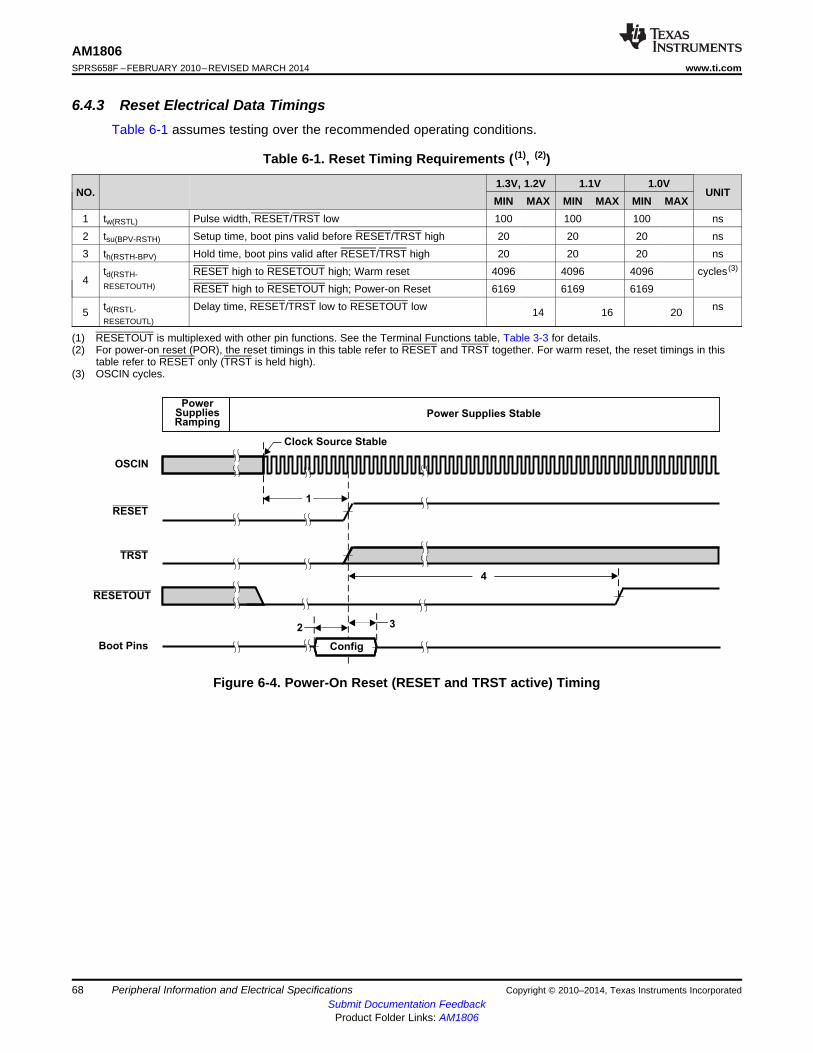
OSCIN
RESET
RESETOUT
Boot Pins Config
PowerSuppliesRamping
Power Supplies Stable
Clock Source Stable
1
2 3
4
TRST
AM1806SPRS658F –FEBRUARY 2010–REVISED MARCH 2014 www.ti.com
6.4.3 Reset Electrical Data TimingsTable 6-1 assumes testing over the recommended operating conditions.
Table 6-1. Reset Timing Requirements ( (1), (2))
1.3V, 1.2V 1.1V 1.0VNO. UNIT
MIN MAX MIN MAX MIN MAX1 tw(RSTL) Pulse width, RESET/TRST low 100 100 100 ns2 tsu(BPV-RSTH) Setup time, boot pins valid before RESET/TRST high 20 20 20 ns3 th(RSTH-BPV) Hold time, boot pins valid after RESET/TRST high 20 20 20 ns
td(RSTH- RESET high to RESETOUT high; Warm reset 4096 4096 4096 cycles (3)4
RESETOUTH) RESET high to RESETOUT high; Power-on Reset 6169 6169 6169td(RSTL- Delay time, RESET/TRST low to RESETOUT low ns5 14 16 20RESETOUTL)
(1) RESETOUT is multiplexed with other pin functions. See the Terminal Functions table, Table 3-3 for details.(2) For power-on reset (POR), the reset timings in this table refer to RESET and TRST together. For warm reset, the reset timings in this
table refer to RESET only (TRST is held high).(3) OSCIN cycles.
Figure 6-4. Power-On Reset (RESET and TRST active) Timing
68 Peripheral Information and Electrical Specifications Copyright © 2010–2014, Texas Instruments IncorporatedSubmit Documentation Feedback
Product Folder Links: AM1806
OSCIN
TRST
RESET
RESETOUT
Boot Pins Config
Power Supplies Stable
1
23
4
Driven or Hi-Z
5
AM1806www.ti.com SPRS658F –FEBRUARY 2010–REVISED MARCH 2014
Figure 6-5. Warm Reset (RESET active, TRST high) Timing
Copyright © 2010–2014, Texas Instruments Incorporated Peripheral Information and Electrical Specifications 69Submit Documentation Feedback
Product Folder Links: AM1806
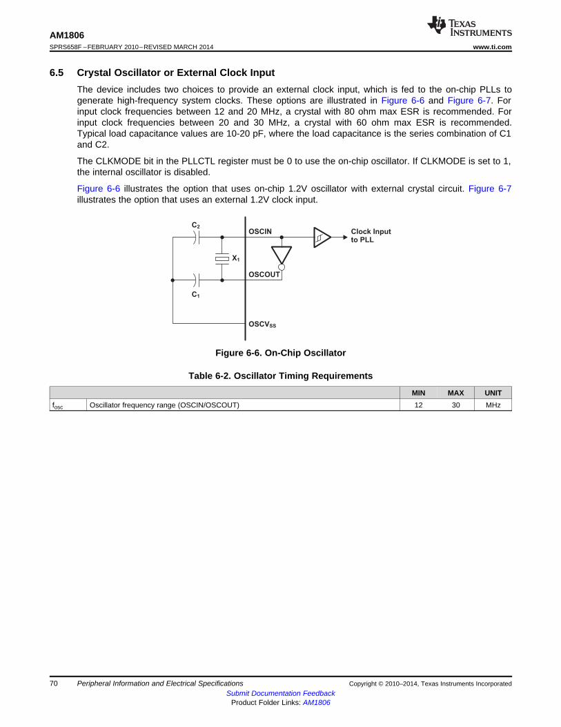
C2
C1
X1
OSCOUT
OSCIN
OSCVSS
Clock Inputto PLL
AM1806SPRS658F –FEBRUARY 2010–REVISED MARCH 2014 www.ti.com
6.5 Crystal Oscillator or External Clock InputThe device includes two choices to provide an external clock input, which is fed to the on-chip PLLs togenerate high-frequency system clocks. These options are illustrated in Figure 6-6 and Figure 6-7. Forinput clock frequencies between 12 and 20 MHz, a crystal with 80 ohm max ESR is recommended. Forinput clock frequencies between 20 and 30 MHz, a crystal with 60 ohm max ESR is recommended.Typical load capacitance values are 10-20 pF, where the load capacitance is the series combination of C1and C2.
The CLKMODE bit in the PLLCTL register must be 0 to use the on-chip oscillator. If CLKMODE is set to 1,the internal oscillator is disabled.
Figure 6-6 illustrates the option that uses on-chip 1.2V oscillator with external crystal circuit. Figure 6-7illustrates the option that uses an external 1.2V clock input.
Figure 6-6. On-Chip Oscillator
Table 6-2. Oscillator Timing Requirements
MIN MAX UNITfosc Oscillator frequency range (OSCIN/OSCOUT) 12 30 MHz
70 Peripheral Information and Electrical Specifications Copyright © 2010–2014, Texas Instruments IncorporatedSubmit Documentation Feedback
Product Folder Links: AM1806
OSCOUT
OSCIN
OSCVSS
ClockInputto PLL
NC
AM1806www.ti.com SPRS658F –FEBRUARY 2010–REVISED MARCH 2014
Figure 6-7. External 1.2V Clock Source
Table 6-3. OSCIN Timing Requirements for an Externally Driven Clock
MIN MAX UNITfOSCIN OSCIN frequency range 12 50 MHztc(OSCIN) Cycle time, external clock driven on OSCIN 20 nstw(OSCINH) Pulse width high, external clock on OSCIN 0.4 tc(OSCIN) nstw(OSCINL) Pulse width low, external clock on OSCIN 0.4 tc(OSCIN) nstt(OSCIN) Transition time, OSCIN 0.25P or 10 (1) nstj(OSCIN) Period jitter, OSCIN 0.02P ns
(1) Whichever is smaller. P = the period of the applied signal. Maintaining transition times as fast as possible is recommended to improvenoise immunity on input signals.
6.6 Clock PLLsThe device has two PLL controllers that provide clocks to different parts of the system. PLL0 providesclocks (though various dividers) to most of the components of the device. PLL1 provides clocks to themDDR/DDR2 Controller and provides an alternate clock source for the ASYNC3 clock domain. This allowsthe peripherals on the ASYNC3 clock domain to be immune to frequency scaling operation on PLL0.
The PLL controller provides the following:• Glitch-Free Transitions (on changing clock settings)• Domain Clocks Alignment• Clock Gating• PLL power down
The various clock outputs given by the controller are as follows:• Domain Clocks: SYSCLK [1:n]• Auxiliary Clock from reference clock source: AUXCLK
Various dividers that can be used are as follows:• Post-PLL Divider: POSTDIV• SYSCLK Divider: D1, ¼, Dn
Various other controls supported are as follows:• PLL Multiplier Control: PLLM• Software programmable PLL Bypass: PLLEN
Copyright © 2010–2014, Texas Instruments Incorporated Peripheral Information and Electrical Specifications 71Submit Documentation Feedback
Product Folder Links: AM1806
0.1µF
0.01µF
50R1.14V - 1.32V
50RVSS
PLL1_VDDA
PLL1_VSSA
Ferrite Bead: Murata BLM31PG500SN1L or Equivalent
0.1µF
0.01µF
50R1.14V - 1.32V
50RVSS
PLL0_VDDA
PLL0_VSSA
AM1806SPRS658F –FEBRUARY 2010–REVISED MARCH 2014 www.ti.com
6.6.1 PLL Device-Specific InformationThe PLL requires some external filtering components to reduce power supply noise as shown in Figure 6-8.
Figure 6-8. PLL External Filtering Components
The external filtering components shown above provide noise immunity for the PLLs. PLL0_VDDA andPLL1_VDDA should not be connected together to provide noise immunity between the two PLLs.Likewise, PLL0_VSSA and PLL1_VSSA should not be connected together.
The input to the PLL is either from the on-chip oscillator or from an external clock on the OSCIN pin. PLL0outputs seven clocks that have programmable divider options. PLL1 outputs three clocks that haveprogrammable divider options. Figure 6-9 illustrates the high-level view of the PLL Topology.
The PLLs are disabled by default after a device reset. They must be configured by software according tothe allowable operating conditions listed in Table 6-4 before enabling the device to run from the PLL bysetting PLLEN = 1.
72 Peripheral Information and Electrical Specifications Copyright © 2010–2014, Texas Instruments IncorporatedSubmit Documentation Feedback
Product Folder Links: AM1806
PLLDIV1 (/1) SYSCLK1
PLLDIV2 (/2) SYSCLK2
PLLDIV4 (/4) SYSCLK4
PLLDIV5 (/3) SYSCLK5
PLLDIV6 (/1) SYSCLK6
PLLDIV7 (/6) SYSCLK7
DIV4.5 1
0EMIFA
InternalClock
Source
CFGCHIP3[EMA_CLKSRC]
1
0
PREDIV
PLLM
1
0
SquareWave
Crystal
PLL1_SYSCLK3
PLLCTL[EXTCLKSRC]
AUXCLK
PLL
PLLDIV3 (/3) SYSCLK3
DDR2/mDDRInternalClock
Source
PLLDIV2 (/2)
PLLDIV3 (/3)
PLLDIV1 (/1)
0
1
PLLCTL[PLLEN]
POSTDIV
PLLM
PLL
0
1
PLLCTL[PLLEN]PLLCTL[CLKMODE]
POSTDIV
PLLC0 OBSCLK(CLKOUT Pin)
DIV4.5OSCDIV
PLL Controller 0
PLL Controller 1
SYSCLK2
SYSCLK3
SYSCLK1
OSCIN
14h
17h
18h
19h
1Ah
1Bh
1Ch
1Dh
1Eh
SYSCLK1SYSCLK2
SYSCLK3
SYSCLK4
SYSCLK5
SYSCLK6
SYSCLK7
PLLC1 OBSCLK
OCSEL[OCSRC]
14h
17h
18h
19h
SYSCLK1SYSCLK2
SYSCLK3
OCSEL[OCSRC]
OSCDIV PLLC1 OBSCLK
DEEPSLEEPEnable
AM1806www.ti.com SPRS658F –FEBRUARY 2010–REVISED MARCH 2014
Figure 6-9. PLL Topology
Copyright © 2010–2014, Texas Instruments Incorporated Peripheral Information and Electrical Specifications 73Submit Documentation Feedback
Product Folder Links: AM1806
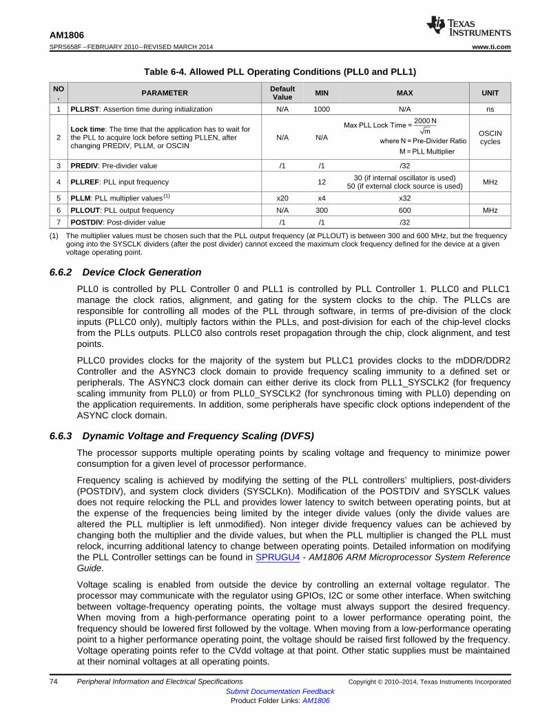
2000 NMax PLL Lock Time =
m
where N = Pre-Divider Ratio
M = PLL Multiplier
AM1806SPRS658F –FEBRUARY 2010–REVISED MARCH 2014 www.ti.com
Table 6-4. Allowed PLL Operating Conditions (PLL0 and PLL1)
NO DefaultPARAMETER MIN MAX UNIT. Value1 PLLRST: Assertion time during initialization N/A 1000 N/A ns
Lock time: The time that the application has to wait for OSCIN2 the PLL to acquire lock before setting PLLEN, after N/A N/A cycleschanging PREDIV, PLLM, or OSCIN
3 PREDIV: Pre-divider value /1 /1 /3230 (if internal oscillator is used)4 PLLREF: PLL input frequency 12 MHz50 (if external clock source is used)
5 PLLM: PLL multiplier values (1) x20 x4 x326 PLLOUT: PLL output frequency N/A 300 600 MHz7 POSTDIV: Post-divider value /1 /1 /32
(1) The multiplier values must be chosen such that the PLL output frequency (at PLLOUT) is between 300 and 600 MHz, but the frequencygoing into the SYSCLK dividers (after the post divider) cannot exceed the maximum clock frequency defined for the device at a givenvoltage operating point.
6.6.2 Device Clock GenerationPLL0 is controlled by PLL Controller 0 and PLL1 is controlled by PLL Controller 1. PLLC0 and PLLC1manage the clock ratios, alignment, and gating for the system clocks to the chip. The PLLCs areresponsible for controlling all modes of the PLL through software, in terms of pre-division of the clockinputs (PLLC0 only), multiply factors within the PLLs, and post-division for each of the chip-level clocksfrom the PLLs outputs. PLLC0 also controls reset propagation through the chip, clock alignment, and testpoints.
PLLC0 provides clocks for the majority of the system but PLLC1 provides clocks to the mDDR/DDR2Controller and the ASYNC3 clock domain to provide frequency scaling immunity to a defined set orperipherals. The ASYNC3 clock domain can either derive its clock from PLL1_SYSCLK2 (for frequencyscaling immunity from PLL0) or from PLL0_SYSCLK2 (for synchronous timing with PLL0) depending onthe application requirements. In addition, some peripherals have specific clock options independent of theASYNC clock domain.
6.6.3 Dynamic Voltage and Frequency Scaling (DVFS)The processor supports multiple operating points by scaling voltage and frequency to minimize powerconsumption for a given level of processor performance.
Frequency scaling is achieved by modifying the setting of the PLL controllers’ multipliers, post-dividers(POSTDIV), and system clock dividers (SYSCLKn). Modification of the POSTDIV and SYSCLK valuesdoes not require relocking the PLL and provides lower latency to switch between operating points, but atthe expense of the frequencies being limited by the integer divide values (only the divide values arealtered the PLL multiplier is left unmodified). Non integer divide frequency values can be achieved bychanging both the multiplier and the divide values, but when the PLL multiplier is changed the PLL mustrelock, incurring additional latency to change between operating points. Detailed information on modifyingthe PLL Controller settings can be found in SPRUGU4 - AM1806 ARM Microprocessor System ReferenceGuide.
Voltage scaling is enabled from outside the device by controlling an external voltage regulator. Theprocessor may communicate with the regulator using GPIOs, I2C or some other interface. When switchingbetween voltage-frequency operating points, the voltage must always support the desired frequency.When moving from a high-performance operating point to a lower performance operating point, thefrequency should be lowered first followed by the voltage. When moving from a low-performance operatingpoint to a higher performance operating point, the voltage should be raised first followed by the frequency.Voltage operating points refer to the CVdd voltage at that point. Other static supplies must be maintainedat their nominal voltages at all operating points.
74 Peripheral Information and Electrical Specifications Copyright © 2010–2014, Texas Instruments IncorporatedSubmit Documentation Feedback
Product Folder Links: AM1806

AM1806www.ti.com SPRS658F –FEBRUARY 2010–REVISED MARCH 2014
The maximum voltage slew rate for CVdd supply changes is 1 mV/us.
For additional information on power management solutions from TI for this processor, follow the PowerManagement link in the Product Folder on www.ti.com for this processor.
The processor supports multiple clock domains some of which have clock ratio requirements to eachother. PLL0_SYSCLK2:PLL0_SYSCLK4:PLL0_SYSCLK6 are synchronous to each other and theSYSCLKn dividers must always be configured such that the ratio between these domains is 2:4:1. TheASYNC and ASYNC3 clock domains are asynchronous to the other clock domains and have no specificratio requirement.
The table below summarizes the maximum internal clock frequencies at each of the voltage operatingpoints.
Table 6-5. Maximum Internal Clock Frequencies at Each Voltage Operating Point
CLOCK SOURCE CLOCK DOMAIN 1.3V NOM 1.2V NOM 1.1V NOM 1.0V NOMPLL0_SYSCLK1 Not used on this processor - - - -
SYSCLK2 clock domain peripherals and optional clock sourcePLL0_SYSCLK2 228 MHz 187.5 MHz 100 MHz 50 MHzfor ASYNC3 clock domain peripheralsPLL0_SYSCLK3 Optional clock for ASYNC1 clock domainPLL0_SYSCLK4 SYSCLK4 domain peripherals 114 MHz 93.75 MHz 50 MHz 25 MHzPLL0_SYSCLK5 Not used on this processor - - - -PLL0_SYSCLK6 ARM subsystem 456 MHz 375 MHz 200 MHz 100 MHzPLL0_SYSCLK7 Not used on this processor - - - -
DDR2/mDDR Interface clock source (memory interface clockPLL1_SYSCLK1 312 MHz 312 MHz 300 MHz 266 MHzis one-half of the value shown)PLL1_SYSCLK2 Optional clock source for ASYNC3 clock domain peripherals 152 MHz 150 MHz 100 MHz 75 MHzPLL1_SYSCLK3 Alternate clock source input to PLL Controller 0 75 MHz 75 MHz 75 MHz 75 MHzMcASP AUXCLK Bypass clock source for the McASP 50 MHz 50 MHz 50 MHz 50 MHzPLL0_AUXCLK Bypass clock source for the USB0 48 MHz 48 MHz 48 MHz 48 MHz
Async Mode 148 MHz 148 MHz 75 MHz 50 MHzASYNC1 ASYNC1 Clock Domain (EMIFA)
SDRAM Mode 100 MHz 100 MHz 66.6 MHz 50 MHzASYNC2 ASYNC2 Clock Domain (multiple peripherals) 50 MHz 50 MHz 50 MHz 50 MHz
Some interfaces have specific limitations on supported modes/speeds at each operating point. See thecorresponding peripheral sections of this document for more information.
TI provides software components (called the Power Manager) to perform DVFS and abstract the task fromthe user. The Power Manager controls changing operating points (both frequency and voltage) andhandles the related tasks involved such as informing/controlling peripherals to provide graceful transitionsbetween operating points.
Copyright © 2010–2014, Texas Instruments Incorporated Peripheral Information and Electrical Specifications 75Submit Documentation Feedback
Product Folder Links: AM1806
AM1806SPRS658F –FEBRUARY 2010–REVISED MARCH 2014 www.ti.com
6.7 Interrupts
6.7.1 ARM CPU InterruptsThe ARM9 CPU core supports 2 direct interrupts: FIQ and IRQ. The ARM Interrupt Controller (AINTC)extends the number of interrupts to 100, and provides features like programmable masking, priority,hardware nesting support, and interrupt vector generation.
6.7.1.1 ARM Interrupt Controller (AINTC) Interrupt Signal Hierarchy
The ARM Interrupt controller organizes interrupts into the following hierarchy:• Peripheral Interrupt Requests
– Individual Interrupt Sources from Peripherals• 101 System Interrupts
– One or more Peripheral Interrupt Requests are combined (fixed configuration) to generate aSystem Interrupt.
– After prioritization, the AINTC will provide an interrupt vector based unique to each System Interrupt• 32 Interrupt Channels
– Each System Interrupt is mapped to one of the 32 Interrupt Channels– Channel Number determines the first level of prioritization, Channel 0 is highest priority and 31
lowest.– If more than one system interrupt is mapped to a channel, priority within the channel is determined
by system interrupt number (0 highest priority)• Host Interrupts (FIQ and IRQ)
– Interrupt Channels 0 and 1 generate the ARM FIQ interrupt– Interrupt Channels 2 through 31 Generate the ARM IRQ interrupt
• Debug Interrupts– Two Debug Interrupts are supported and can be used to trigger events in the debug subsystem– Sources can be selected from any of the System Interrupts or Host Interrupts
6.7.1.2 AINTC Hardware Vector Generation
The AINTC also generates an interrupt vector in hardware for both IRQ and FIQ host interrupts. This maybe used to accelerate interrupt dispatch. A unique vector is generated for each of the 100 systeminterrupts. The vector is computed in hardware as:
VECTOR = BASE + (SYSTEM INTERRUPT NUMBER × SIZE)
Where BASE and SIZE are programmable. The computed vector is a 32-bit address which maydispatched to using a single instruction of type LDR PC, [PC, #-<offset_12>] at the FIQ and IRQ vectorlocations (0xFFFF0018 and 0xFFFF001C respectively).
6.7.1.3 AINTC Hardware Interrupt Nesting Support
Interrupt nesting occurs when an interrupt service routine re-enables interrupts, to allow the CPU tointerrupt the ISR if a higher priority event occurs. The AINTC provides hardware support to facilitateinterrupt nesting. It supports both global and per host interrupt (FIQ and IRQ in this case) automaticnesting. If enabled, the AINTC will automatically update an internal nesting register that temporarily masksinterrupts at and below the priority of the current interrupt channel. Then if the ISR re-enables interrupts;only higher priority channels will be able to interrupt it. The nesting level is restored by the ISR by writingto the nesting level register on completion. Support for nesting can be enabled/disabled by software, withthe option of automatic nesting on a global or per host interrupt basis; or manual nesting.
76 Peripheral Information and Electrical Specifications Copyright © 2010–2014, Texas Instruments IncorporatedSubmit Documentation Feedback
Product Folder Links: AM1806
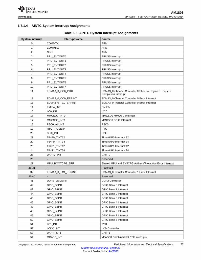
AM1806www.ti.com SPRS658F –FEBRUARY 2010–REVISED MARCH 2014
6.7.1.4 AINTC System Interrupt Assignments
Table 6-6. AINTC System Interrupt Assignments
System Interrupt Interrupt Name Source0 COMMTX ARM1 COMMRX ARM2 NINT ARM3 PRU_EVTOUT0 PRUSS Interrupt4 PRU_EVTOUT1 PRUSS Interrupt5 PRU_EVTOUT2 PRUSS Interrupt6 PRU_EVTOUT3 PRUSS Interrupt7 PRU_EVTOUT4 PRUSS Interrupt8 PRU_EVTOUT5 PRUSS Interrupt9 PRU_EVTOUT6 PRUSS Interrupt
10 PRU_EVTOUT7 PRUSS Interrupt11 EDMA3_0_CC0_INT0 EDMA3_0 Channel Controller 0 Shadow Region 0 Transfer
Completion Interrupt12 EDMA3_0_CC0_ERRINT EDMA3_0 Channel Controller 0 Error Interrupt13 EDMA3_0_TC0_ERRINT EDMA3_0 Transfer Controller 0 Error Interrupt14 EMIFA_INT EMIFA15 IIC0_INT I2C016 MMCSD0_INT0 MMCSD0 MMC/SD Interrupt17 MMCSD0_INT1 MMCSD0 SDIO Interrupt18 PSC0_ALLINT PSC019 RTC_IRQS[1:0] RTC20 SPI0_INT SPI021 T64P0_TINT12 Timer64P0 Interrupt 1222 T64P0_TINT34 Timer64P0 Interrupt 3423 T64P1_TINT12 Timer64P1 Interrupt 1224 T64P1_TINT34 Timer64P1 Interrupt 3425 UART0_INT UART026 - Reserved27 MPU_BOOTCFG_ERR Shared MPU and SYSCFG Address/Protection Error Interrupt
28-31 - Reserved32 EDMA3_0_TC1_ERRINT EDMA3_0 Transfer Controller 1 Error Interrupt
33-40 - Reserved41 DDR2_MEMERR DDR2 Controller42 GPIO_B0INT GPIO Bank 0 Interrupt43 GPIO_B1INT GPIO Bank 1 Interrupt44 GPIO_B2INT GPIO Bank 2 Interrupt45 GPIO_B3INT GPIO Bank 3 Interrupt46 GPIO_B4INT GPIO Bank 4 Interrupt47 GPIO_B5INT GPIO Bank 5 Interrupt48 GPIO_B6INT GPIO Bank 6 Interrupt49 GPIO_B7INT GPIO Bank 7 Interrupt50 GPIO_B8INT GPIO Bank 8 Interrupt51 IIC1_INT I2C152 LCDC_INT LCD Controller53 UART_INT1 UART154 MCASP_INT McASP0 Combined RX / TX Interrupts
Copyright © 2010–2014, Texas Instruments Incorporated Peripheral Information and Electrical Specifications 77Submit Documentation Feedback
Product Folder Links: AM1806
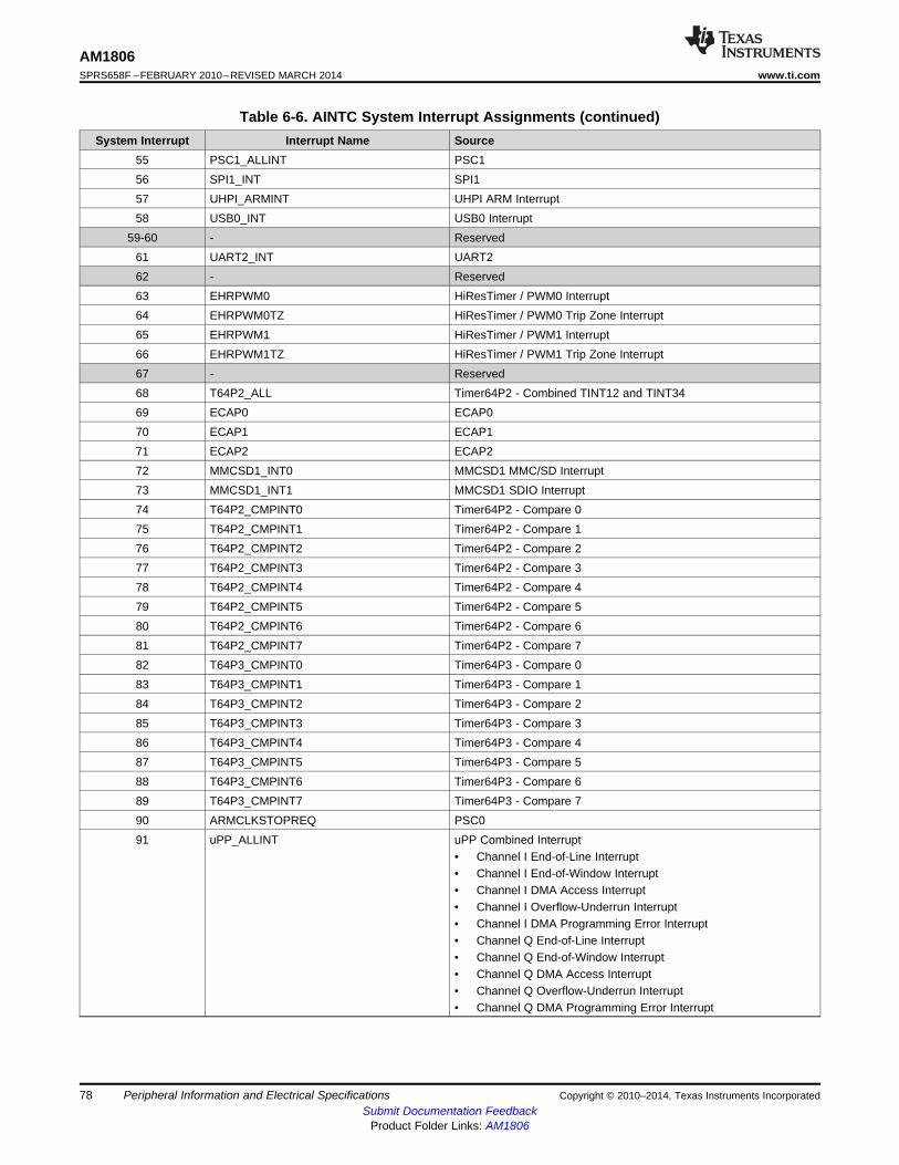
AM1806SPRS658F –FEBRUARY 2010–REVISED MARCH 2014 www.ti.com
Table 6-6. AINTC System Interrupt Assignments (continued)System Interrupt Interrupt Name Source
55 PSC1_ALLINT PSC156 SPI1_INT SPI157 UHPI_ARMINT UHPI ARM Interrupt58 USB0_INT USB0 Interrupt
59-60 - Reserved61 UART2_INT UART262 - Reserved63 EHRPWM0 HiResTimer / PWM0 Interrupt64 EHRPWM0TZ HiResTimer / PWM0 Trip Zone Interrupt65 EHRPWM1 HiResTimer / PWM1 Interrupt66 EHRPWM1TZ HiResTimer / PWM1 Trip Zone Interrupt67 - Reserved68 T64P2_ALL Timer64P2 - Combined TINT12 and TINT3469 ECAP0 ECAP070 ECAP1 ECAP171 ECAP2 ECAP272 MMCSD1_INT0 MMCSD1 MMC/SD Interrupt73 MMCSD1_INT1 MMCSD1 SDIO Interrupt74 T64P2_CMPINT0 Timer64P2 - Compare 075 T64P2_CMPINT1 Timer64P2 - Compare 176 T64P2_CMPINT2 Timer64P2 - Compare 277 T64P2_CMPINT3 Timer64P2 - Compare 378 T64P2_CMPINT4 Timer64P2 - Compare 479 T64P2_CMPINT5 Timer64P2 - Compare 580 T64P2_CMPINT6 Timer64P2 - Compare 681 T64P2_CMPINT7 Timer64P2 - Compare 782 T64P3_CMPINT0 Timer64P3 - Compare 083 T64P3_CMPINT1 Timer64P3 - Compare 184 T64P3_CMPINT2 Timer64P3 - Compare 285 T64P3_CMPINT3 Timer64P3 - Compare 386 T64P3_CMPINT4 Timer64P3 - Compare 487 T64P3_CMPINT5 Timer64P3 - Compare 588 T64P3_CMPINT6 Timer64P3 - Compare 689 T64P3_CMPINT7 Timer64P3 - Compare 790 ARMCLKSTOPREQ PSC091 uPP_ALLINT uPP Combined Interrupt
• Channel I End-of-Line Interrupt• Channel I End-of-Window Interrupt• Channel I DMA Access Interrupt• Channel I Overflow-Underrun Interrupt• Channel I DMA Programming Error Interrupt• Channel Q End-of-Line Interrupt• Channel Q End-of-Window Interrupt• Channel Q DMA Access Interrupt• Channel Q Overflow-Underrun Interrupt• Channel Q DMA Programming Error Interrupt
78 Peripheral Information and Electrical Specifications Copyright © 2010–2014, Texas Instruments IncorporatedSubmit Documentation Feedback
Product Folder Links: AM1806
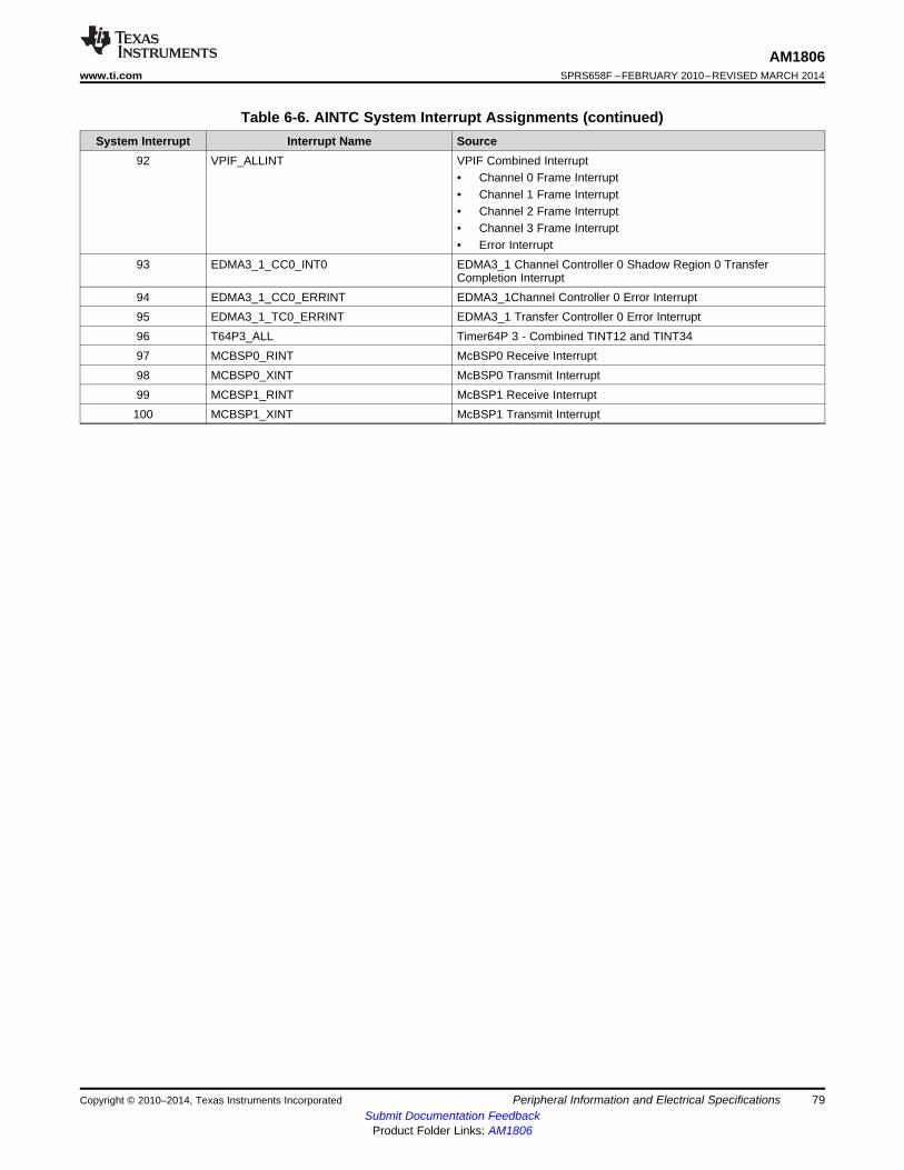
AM1806www.ti.com SPRS658F –FEBRUARY 2010–REVISED MARCH 2014
Table 6-6. AINTC System Interrupt Assignments (continued)System Interrupt Interrupt Name Source
92 VPIF_ALLINT VPIF Combined Interrupt• Channel 0 Frame Interrupt• Channel 1 Frame Interrupt• Channel 2 Frame Interrupt• Channel 3 Frame Interrupt• Error Interrupt
93 EDMA3_1_CC0_INT0 EDMA3_1 Channel Controller 0 Shadow Region 0 TransferCompletion Interrupt
94 EDMA3_1_CC0_ERRINT EDMA3_1Channel Controller 0 Error Interrupt95 EDMA3_1_TC0_ERRINT EDMA3_1 Transfer Controller 0 Error Interrupt96 T64P3_ALL Timer64P 3 - Combined TINT12 and TINT3497 MCBSP0_RINT McBSP0 Receive Interrupt98 MCBSP0_XINT McBSP0 Transmit Interrupt99 MCBSP1_RINT McBSP1 Receive Interrupt100 MCBSP1_XINT McBSP1 Transmit Interrupt
Copyright © 2010–2014, Texas Instruments Incorporated Peripheral Information and Electrical Specifications 79Submit Documentation Feedback
Product Folder Links: AM1806
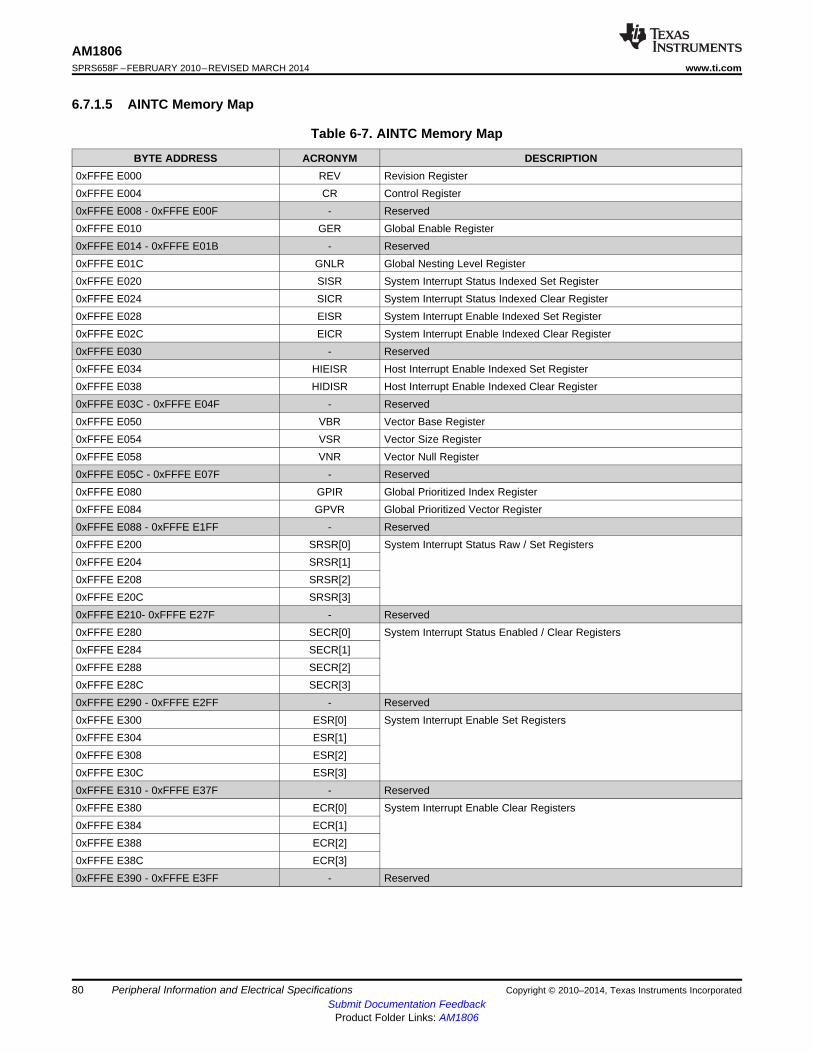
AM1806SPRS658F –FEBRUARY 2010–REVISED MARCH 2014 www.ti.com
6.7.1.5 AINTC Memory Map
Table 6-7. AINTC Memory Map
BYTE ADDRESS ACRONYM DESCRIPTION0xFFFE E000 REV Revision Register0xFFFE E004 CR Control Register0xFFFE E008 - 0xFFFE E00F - Reserved0xFFFE E010 GER Global Enable Register0xFFFE E014 - 0xFFFE E01B - Reserved0xFFFE E01C GNLR Global Nesting Level Register0xFFFE E020 SISR System Interrupt Status Indexed Set Register0xFFFE E024 SICR System Interrupt Status Indexed Clear Register0xFFFE E028 EISR System Interrupt Enable Indexed Set Register0xFFFE E02C EICR System Interrupt Enable Indexed Clear Register0xFFFE E030 - Reserved0xFFFE E034 HIEISR Host Interrupt Enable Indexed Set Register0xFFFE E038 HIDISR Host Interrupt Enable Indexed Clear Register0xFFFE E03C - 0xFFFE E04F - Reserved0xFFFE E050 VBR Vector Base Register0xFFFE E054 VSR Vector Size Register0xFFFE E058 VNR Vector Null Register0xFFFE E05C - 0xFFFE E07F - Reserved0xFFFE E080 GPIR Global Prioritized Index Register0xFFFE E084 GPVR Global Prioritized Vector Register0xFFFE E088 - 0xFFFE E1FF - Reserved0xFFFE E200 SRSR[0] System Interrupt Status Raw / Set Registers0xFFFE E204 SRSR[1]0xFFFE E208 SRSR[2]0xFFFE E20C SRSR[3]0xFFFE E210- 0xFFFE E27F - Reserved0xFFFE E280 SECR[0] System Interrupt Status Enabled / Clear Registers0xFFFE E284 SECR[1]0xFFFE E288 SECR[2]0xFFFE E28C SECR[3]0xFFFE E290 - 0xFFFE E2FF - Reserved0xFFFE E300 ESR[0] System Interrupt Enable Set Registers0xFFFE E304 ESR[1]0xFFFE E308 ESR[2]0xFFFE E30C ESR[3]0xFFFE E310 - 0xFFFE E37F - Reserved0xFFFE E380 ECR[0] System Interrupt Enable Clear Registers0xFFFE E384 ECR[1]0xFFFE E388 ECR[2]0xFFFE E38C ECR[3]0xFFFE E390 - 0xFFFE E3FF - Reserved
80 Peripheral Information and Electrical Specifications Copyright © 2010–2014, Texas Instruments IncorporatedSubmit Documentation Feedback
Product Folder Links: AM1806
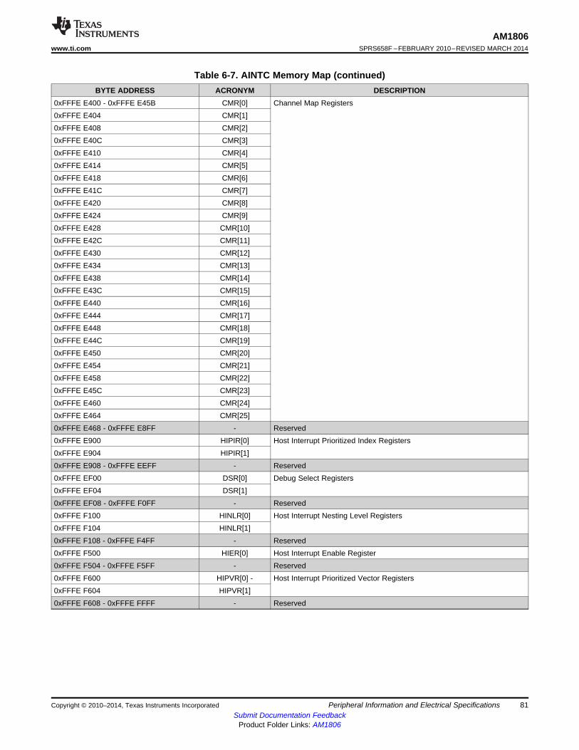
AM1806www.ti.com SPRS658F –FEBRUARY 2010–REVISED MARCH 2014
Table 6-7. AINTC Memory Map (continued)BYTE ADDRESS ACRONYM DESCRIPTION
0xFFFE E400 - 0xFFFE E45B CMR[0] Channel Map Registers0xFFFE E404 CMR[1]0xFFFE E408 CMR[2]0xFFFE E40C CMR[3]0xFFFE E410 CMR[4]0xFFFE E414 CMR[5]0xFFFE E418 CMR[6]0xFFFE E41C CMR[7]0xFFFE E420 CMR[8]0xFFFE E424 CMR[9]0xFFFE E428 CMR[10]0xFFFE E42C CMR[11]0xFFFE E430 CMR[12]0xFFFE E434 CMR[13]0xFFFE E438 CMR[14]0xFFFE E43C CMR[15]0xFFFE E440 CMR[16]0xFFFE E444 CMR[17]0xFFFE E448 CMR[18]0xFFFE E44C CMR[19]0xFFFE E450 CMR[20]0xFFFE E454 CMR[21]0xFFFE E458 CMR[22]0xFFFE E45C CMR[23]0xFFFE E460 CMR[24]0xFFFE E464 CMR[25]0xFFFE E468 - 0xFFFE E8FF - Reserved0xFFFE E900 HIPIR[0] Host Interrupt Prioritized Index Registers0xFFFE E904 HIPIR[1]0xFFFE E908 - 0xFFFE EEFF - Reserved0xFFFE EF00 DSR[0] Debug Select Registers0xFFFE EF04 DSR[1]0xFFFE EF08 - 0xFFFE F0FF - Reserved0xFFFE F100 HINLR[0] Host Interrupt Nesting Level Registers0xFFFE F104 HINLR[1]0xFFFE F108 - 0xFFFE F4FF - Reserved0xFFFE F500 HIER[0] Host Interrupt Enable Register0xFFFE F504 - 0xFFFE F5FF - Reserved0xFFFE F600 HIPVR[0] - Host Interrupt Prioritized Vector Registers0xFFFE F604 HIPVR[1]0xFFFE F608 - 0xFFFE FFFF - Reserved
Copyright © 2010–2014, Texas Instruments Incorporated Peripheral Information and Electrical Specifications 81Submit Documentation Feedback
Product Folder Links: AM1806
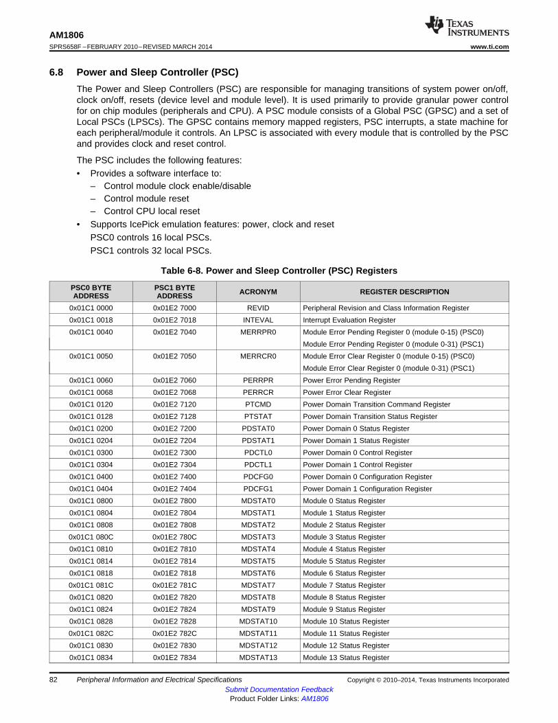
AM1806SPRS658F –FEBRUARY 2010–REVISED MARCH 2014 www.ti.com
6.8 Power and Sleep Controller (PSC)The Power and Sleep Controllers (PSC) are responsible for managing transitions of system power on/off,clock on/off, resets (device level and module level). It is used primarily to provide granular power controlfor on chip modules (peripherals and CPU). A PSC module consists of a Global PSC (GPSC) and a set ofLocal PSCs (LPSCs). The GPSC contains memory mapped registers, PSC interrupts, a state machine foreach peripheral/module it controls. An LPSC is associated with every module that is controlled by the PSCand provides clock and reset control.
The PSC includes the following features:• Provides a software interface to:
– Control module clock enable/disable– Control module reset– Control CPU local reset
• Supports IcePick emulation features: power, clock and resetPSC0 controls 16 local PSCs.PSC1 controls 32 local PSCs.
Table 6-8. Power and Sleep Controller (PSC) Registers
PSC0 BYTE PSC1 BYTE ACRONYM REGISTER DESCRIPTIONADDRESS ADDRESS0x01C1 0000 0x01E2 7000 REVID Peripheral Revision and Class Information Register0x01C1 0018 0x01E2 7018 INTEVAL Interrupt Evaluation Register0x01C1 0040 0x01E2 7040 MERRPR0 Module Error Pending Register 0 (module 0-15) (PSC0)
Module Error Pending Register 0 (module 0-31) (PSC1)0x01C1 0050 0x01E2 7050 MERRCR0 Module Error Clear Register 0 (module 0-15) (PSC0)
Module Error Clear Register 0 (module 0-31) (PSC1)0x01C1 0060 0x01E2 7060 PERRPR Power Error Pending Register0x01C1 0068 0x01E2 7068 PERRCR Power Error Clear Register0x01C1 0120 0x01E2 7120 PTCMD Power Domain Transition Command Register0x01C1 0128 0x01E2 7128 PTSTAT Power Domain Transition Status Register0x01C1 0200 0x01E2 7200 PDSTAT0 Power Domain 0 Status Register0x01C1 0204 0x01E2 7204 PDSTAT1 Power Domain 1 Status Register0x01C1 0300 0x01E2 7300 PDCTL0 Power Domain 0 Control Register0x01C1 0304 0x01E2 7304 PDCTL1 Power Domain 1 Control Register0x01C1 0400 0x01E2 7400 PDCFG0 Power Domain 0 Configuration Register0x01C1 0404 0x01E2 7404 PDCFG1 Power Domain 1 Configuration Register0x01C1 0800 0x01E2 7800 MDSTAT0 Module 0 Status Register0x01C1 0804 0x01E2 7804 MDSTAT1 Module 1 Status Register0x01C1 0808 0x01E2 7808 MDSTAT2 Module 2 Status Register0x01C1 080C 0x01E2 780C MDSTAT3 Module 3 Status Register0x01C1 0810 0x01E2 7810 MDSTAT4 Module 4 Status Register0x01C1 0814 0x01E2 7814 MDSTAT5 Module 5 Status Register0x01C1 0818 0x01E2 7818 MDSTAT6 Module 6 Status Register0x01C1 081C 0x01E2 781C MDSTAT7 Module 7 Status Register0x01C1 0820 0x01E2 7820 MDSTAT8 Module 8 Status Register0x01C1 0824 0x01E2 7824 MDSTAT9 Module 9 Status Register0x01C1 0828 0x01E2 7828 MDSTAT10 Module 10 Status Register0x01C1 082C 0x01E2 782C MDSTAT11 Module 11 Status Register0x01C1 0830 0x01E2 7830 MDSTAT12 Module 12 Status Register0x01C1 0834 0x01E2 7834 MDSTAT13 Module 13 Status Register
82 Peripheral Information and Electrical Specifications Copyright © 2010–2014, Texas Instruments IncorporatedSubmit Documentation Feedback
Product Folder Links: AM1806

AM1806www.ti.com SPRS658F –FEBRUARY 2010–REVISED MARCH 2014
Table 6-8. Power and Sleep Controller (PSC) Registers (continued)PSC0 BYTE PSC1 BYTE ACRONYM REGISTER DESCRIPTIONADDRESS ADDRESS0x01C1 0838 0x01E2 7838 MDSTAT14 Module 14 Status Register0x01C1 083C 0x01E2 783C MDSTAT15 Module 15 Status Register
- 0x01E2 7840 MDSTAT16 Module 16 Status Register- 0x01E2 7844 MDSTAT17 Module 17 Status Register- 0x01E2 7848 MDSTAT18 Module 18 Status Register- 0x01E2 784C MDSTAT19 Module 19 Status Register- 0x01E2 7850 MDSTAT20 Module 20 Status Register- 0x01E2 7854 MDSTAT21 Module 21 Status Register- 0x01E2 7858 MDSTAT22 Module 22 Status Register- 0x01E2 785C MDSTAT23 Module 23 Status Register- 0x01E2 7860 MDSTAT24 Module 24 Status Register- 0x01E2 7864 MDSTAT25 Module 25 Status Register- 0x01E2 7868 MDSTAT26 Module 26 Status Register- 0x01E2 786C MDSTAT27 Module 27 Status Register- 0x01E2 7870 MDSTAT28 Module 28 Status Register- 0x01E2 7874 MDSTAT29 Module 29 Status Register- 0x01E2 7878 MDSTAT30 Module 30 Status Register- 0x01E2 787C MDSTAT31 Module 31 Status Register
0x01C1 0A00 0x01E2 7A00 MDCTL0 Module 0 Control Register0x01C1 0A04 0x01E2 7A04 MDCTL1 Module 1 Control Register0x01C1 0A08 0x01E2 7A08 MDCTL2 Module 2 Control Register0x01C1 0A0C 0x01E2 7A0C MDCTL3 Module 3 Control Register0x01C1 0A10 0x01E2 7A10 MDCTL4 Module 4 Control Register0x01C1 0A14 0x01E2 7A14 MDCTL5 Module 5 Control Register0x01C1 0A18 0x01E2 7A18 MDCTL6 Module 6 Control Register0x01C1 0A1C 0x01E2 7A1C MDCTL7 Module 7 Control Register0x01C1 0A20 0x01E2 7A20 MDCTL8 Module 8 Control Register0x01C1 0A24 0x01E2 7A24 MDCTL9 Module 9 Control Register0x01C1 0A28 0x01E2 7A28 MDCTL10 Module 10 Control Register0x01C1 0A2C 0x01E2 7A2C MDCTL11 Module 11 Control Register0x01C1 0A30 0x01E2 7A30 MDCTL12 Module 12 Control Register0x01C1 0A34 0x01E2 7A34 MDCTL13 Module 13 Control Register0x01C1 0A38 0x01E2 7A38 MDCTL14 Module 14 Control Register0x01C1 0A3C 0x01E2 7A3C MDCTL15 Module 15 Control Register
- 0x01E2 7A40 MDCTL16 Module 16 Control Register- 0x01E2 7A44 MDCTL17 Module 17 Control Register- 0x01E2 7A48 MDCTL18 Module 18 Control Register- 0x01E2 7A4C MDCTL19 Module 19 Control Register- 0x01E2 7A50 MDCTL20 Module 20 Control Register- 0x01E2 7A54 MDCTL21 Module 21 Control Register- 0x01E2 7A58 MDCTL22 Module 22 Control Register- 0x01E2 7A5C MDCTL23 Module 23 Control Register- 0x01E2 7A60 MDCTL24 Module 24 Control Register- 0x01E2 7A64 MDCTL25 Module 25 Control Register- 0x01E2 7A68 MDCTL26 Module 26 Control Register- 0x01E2 7A6C MDCTL27 Module 27 Control Register- 0x01E2 7A70 MDCTL28 Module 28 Control Register
Copyright © 2010–2014, Texas Instruments Incorporated Peripheral Information and Electrical Specifications 83Submit Documentation Feedback
Product Folder Links: AM1806
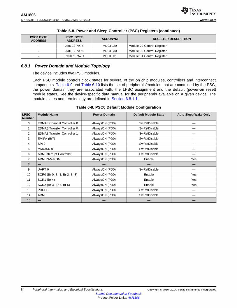
AM1806SPRS658F –FEBRUARY 2010–REVISED MARCH 2014 www.ti.com
Table 6-8. Power and Sleep Controller (PSC) Registers (continued)PSC0 BYTE PSC1 BYTE ACRONYM REGISTER DESCRIPTIONADDRESS ADDRESS
- 0x01E2 7A74 MDCTL29 Module 29 Control Register- 0x01E2 7A78 MDCTL30 Module 30 Control Register- 0x01E2 7A7C MDCTL31 Module 31 Control Register
6.8.1 Power Domain and Module TopologyThe device includes two PSC modules.
Each PSC module controls clock states for several of the on chip modules, controllers and interconnectcomponents. Table 6-9 and Table 6-10 lists the set of peripherals/modules that are controlled by the PSC,the power domain they are associated with, the LPSC assignment and the default (power-on reset)module states. See the device-specific data manual for the peripherals available on a given device. Themodule states and terminology are defined in Section 6.8.1.1.
Table 6-9. PSC0 Default Module Configuration
LPSC Module Name Power Domain Default Module State Auto Sleep/Wake OnlyNumber
0 EDMA3 Channel Controller 0 AlwaysON (PD0) SwRstDisable —1 EDMA3 Transfer Controller 0 AlwaysON (PD0) SwRstDisable —2 EDMA3 Transfer Controller 1 AlwaysON (PD0) SwRstDisable —3 EMIFA (Br7) AlwaysON (PD0) SwRstDisable —4 SPI 0 AlwaysON (PD0) SwRstDisable —5 MMC/SD 0 AlwaysON (PD0) SwRstDisable —6 ARM Interrupt Controller AlwaysON (PD0) SwRstDisable —7 ARM RAM/ROM AlwaysON (PD0) Enable Yes8 — — — —9 UART 0 AlwaysON (PD0) SwRstDisable —10 SCR0 (Br 0, Br 1, Br 2, Br 8) AlwaysON (PD0) Enable Yes11 SCR1 (Br 4) AlwaysON (PD0) Enable Yes12 SCR2 (Br 3, Br 5, Br 6) AlwaysON (PD0) Enable Yes13 PRUSS AlwaysON (PD0) SwRstDisable —14 ARM AlwaysON (PD0) SwRstDisable —15 — — — —
84 Peripheral Information and Electrical Specifications Copyright © 2010–2014, Texas Instruments IncorporatedSubmit Documentation Feedback
Product Folder Links: AM1806
AM1806www.ti.com SPRS658F –FEBRUARY 2010–REVISED MARCH 2014
Table 6-10. PSC1 Default Module Configuration
LPSC Module Name Power Domain Default Module State Auto Sleep/Wake OnlyNumber
0 EDMA3 Channel Controller 1 AlwaysON (PD0) SwRstDisable —1 USB0 (USB2.0) AlwaysON (PD0) SwRstDisable —2 — — — —3 GPIO AlwaysON (PD0) SwRstDisable —4 UHPI AlwaysON (PD0) SwRstDisable —5 — — — —6 DDR2 (and SCR_F3) AlwaysON (PD0) SwRstDisable —7 McASP0 ( + McASP0 FIFO) AlwaysON (PD0) SwRstDisable —8 — — — —9 VPIF AlwaysON (PD0) SwRstDisable —10 SPI 1 AlwaysON (PD0) SwRstDisable —11 I2C 1 AlwaysON (PD0) SwRstDisable —12 UART 1 AlwaysON (PD0) SwRstDisable —13 UART 2 AlwaysON (PD0) SwRstDisable —14 McBSP0 ( + McBSP0 FIFO) AlwaysON (PD0) SwRstDisable —15 McBSP1 ( + McBSP1 FIFO) AlwaysON (PD0) SwRstDisable —16 LCDC AlwaysON (PD0) SwRstDisable —17 eHRPWM0/1 AlwaysON (PD0) SwRstDisable —18 MMCSD1 AlwaysON (PD0) SwRstDisable —19 uPP AlwaysON (PD0) SwRstDisable —20 ECAP0/1/2 AlwaysON (PD0) SwRstDisable —21 EDMA3 Transfer Controller 2 AlwaysON (PD0) SwRstDisable —
22-23 — — — —24 SCR_F0 (and bridge F0) AlwaysON (PD0) Enable Yes25 SCR_F1 (and bridge F1) AlwaysON (PD0) Enable Yes26 SCR_F2 (and bridge F2) AlwaysON (PD0) Enable Yes27 SCR_F6 (and bridge F3) AlwaysON (PD0) Enable Yes28 SCR_F7 (and bridge F4) AlwaysON (PD0) Enable Yes29 SCR_F8 (and bridge F5) AlwaysON (PD0) Enable Yes30 Bridge F7 (DDR Controller AlwaysON (PD0) Enable Yes
path)31 On-chip RAM (including PD_SHRAM Enable —
SCR_F4 and bridge F6)
Copyright © 2010–2014, Texas Instruments Incorporated Peripheral Information and Electrical Specifications 85Submit Documentation Feedback
Product Folder Links: AM1806
AM1806SPRS658F –FEBRUARY 2010–REVISED MARCH 2014 www.ti.com
6.8.1.1 Module States
The PSC defines several possible states for a module. This states are essentially a combination of themodule reset asserted or de-asserted and module clock on/enabled or off/disabled. The module states aredefined in Table 6-11.
Table 6-11. Module States
Module State Module Reset Module Module State DefinitionClock
Enable De-asserted On A module in the enable state has its module reset de-asserted and it has its clock on.This is the normal operational state for a given module
Disable De-asserted Off A module in the disabled state has its module reset de-asserted and it has its moduleclock off. This state is typically used for disabling a module clock to save power. Thedevice is designed in full static CMOS, so when you stop a module clock, it retains themodule’s state. When the clock is restarted, the module resumes operating from thestopping point.
SyncReset Asserted On A module state in the SyncReset state has its module reset asserted and it has itsclock on. Generally, software is not expected to initiate this state
SwRstDisable Asserted Off A module in the SwResetDisable state has its module reset asserted and it has itsclock disabled. After initial power-on, several modules come up in the SwRstDisablestate. Generally, software is not expected to initiate this state
Auto Sleep De-asserted Off A module in the Auto Sleep state also has its module reset de-asserted and its moduleclock disabled, similar to the Disable state. However this is a special state, once amodule is configured in this state by software, it can “automatically” transition to“Enable” state whenever there is an internal read/write request made to it, and afterservicing the request it will “automatically” transition into the sleep state (with modulereset re de-asserted and module clock disabled), without any software intervention.The transition from sleep to enabled and back to sleep state has some cycle latencyassociated with it. It is not envisioned to use this mode when peripherals are fullyoperational and moving data.
Auto Wake De-asserted Off A module in the Auto Wake state also has its module reset de-asserted and its moduleclock disabled, similar to the Disable state. However this is a special state, once amodule is configured in this state by software, it will “automatically” transition to“Enable” state whenever there is an internal read/write request made to it, and willremain in the “Enabled” state from then on (with module reset re de-asserted andmodule clock on), without any software intervention. The transition from sleep toenabled state has some cycle latency associated with it. It is not envisioned to use thismode when peripherals are fully operational and moving data.
86 Peripheral Information and Electrical Specifications Copyright © 2010–2014, Texas Instruments IncorporatedSubmit Documentation Feedback
Product Folder Links: AM1806
AM1806www.ti.com SPRS658F –FEBRUARY 2010–REVISED MARCH 2014
6.9 EDMAThe EDMA controller handles all data transfers between memories and the device slave peripherals onthe device. These data transfers include cache servicing, non-cacheable memory accesses, user-programmed data transfers, and host accesses.
6.9.1 EDMA3 Channel Synchronization EventsEach EDMA channel controller supports up to 32 channels which service peripherals and memory.Table 6-12lists the source of the EDMA synchronization events associated with each of the programmableEDMA channels.
Table 6-12. EDMA Synchronization Events
EDMA0 Channel Controller 0Event Event Name / Source Event Event Name / Source
0 McASP0 Receive 16 MMCSD0 Receive1 McASP0 Transmit 17 MMCSD0 Transmit2 McBSP0 Receive 18 SPI1 Receive3 McBSP0 Transmit 19 SPI1 Transmit4 McBSP1 Receive 20 PRU_EVTOUT65 McBSP1 Transmit 21 PRU_EVTOUT76 GPIO Bank 0 Interrupt 22 GPIO Bank 2 Interrupt7 GPIO Bank 1 Interrupt 23 GPIO Bank 3 Interrupt8 UART0 Receive 24 I2C0 Receive9 UART0 Transmit 25 I2C0 Transmit10 Timer64P0 Event Out 12 26 I2C1 Receive11 Timer64P0 Event Out 34 27 I2C1 Transmit12 UART1 Receive 28 GPIO Bank 4 Interrupt13 UART1 Transmit 29 GPIO Bank 5 Interrupt14 SPI0 Receive 30 UART2 Receive15 SPI0 Transmit 31 UART2 Transmit
EDMA1 Channel Controller 1Event Event Name / Source Event Event Name / Source
0 Timer64P2 Compare Event 0 16 GPIO Bank 6 Interrupt1 Timer64P2 Compare Event 1 17 GPIO Bank 7 Interrupt2 Timer64P2 Compare Event 2 18 GPIO Bank 8 Interrupt3 Timer64P2 Compare Event 3 19 Reserved4 Timer64P2 Compare Event 4 20 Reserved5 Timer64P2 Compare Event 5 21 Reserved6 Timer64P2 Compare Event 6 22 Reserved7 Timer64P2 Compare Event 7 23 Reserved8 Timer64P3 Compare Event 0 24 Timer64P2 Event Out 129 Timer64P3 Compare Event 1 25 Timer64P2 Event Out 3410 Timer64P3 Compare Event 2 26 Timer64P3 Event Out 1211 Timer64P3 Compare Event 3 27 Timer64P3 Event Out 3412 Timer64P3 Compare Event 4 28 MMCSD1 Receive13 Timer64P3 Compare Event 5 29 MMCSD1 Transmit14 Timer64P3 Compare Event 6 30 Reserved15 Timer64P3 Compare Event 7 31 Reserved
Copyright © 2010–2014, Texas Instruments Incorporated Peripheral Information and Electrical Specifications 87Submit Documentation Feedback
Product Folder Links: AM1806
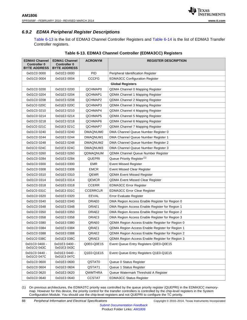
AM1806SPRS658F –FEBRUARY 2010–REVISED MARCH 2014 www.ti.com
6.9.2 EDMA Peripheral Register DescriptionsTable 6-13 is the list of EDMA3 Channel Controller Registers and Table 6-14 is the list of EDMA3 TransferController registers.
Table 6-13. EDMA3 Channel Controller (EDMA3CC) Registers
EDMA0 Channel EDMA1 Channel ACRONYM REGISTER DESCRIPTIONController 0 Controller 0
BYTE ADDRESS BYTE ADDRESS0x01C0 0000 0x01E3 0000 PID Peripheral Identification Register0x01C0 0004 0x01E3 0004 CCCFG EDMA3CC Configuration Register
Global Registers0x01C0 0200 0x01E3 0200 QCHMAP0 QDMA Channel 0 Mapping Register0x01C0 0204 0x01E3 0204 QCHMAP1 QDMA Channel 1 Mapping Register0x01C0 0208 0x01E3 0208 QCHMAP2 QDMA Channel 2 Mapping Register0x01C0 020C 0x01E3 020C QCHMAP3 QDMA Channel 3 Mapping Register0x01C0 0210 0x01E3 0210 QCHMAP4 QDMA Channel 4 Mapping Register0x01C0 0214 0x01E3 0214 QCHMAP5 QDMA Channel 5 Mapping Register0x01C0 0218 0x01E3 0218 QCHMAP6 QDMA Channel 6 Mapping Register0x01C0 021C 0x01E3 021C QCHMAP7 QDMA Channel 7 Mapping Register0x01C0 0240 0x01E3 0240 DMAQNUM0 DMA Channel Queue Number Register 00x01C0 0244 0x01E3 0244 DMAQNUM1 DMA Channel Queue Number Register 10x01C0 0248 0x01E3 0248 DMAQNUM2 DMA Channel Queue Number Register 20x01C0 024C 0x01E3 024C DMAQNUM3 DMA Channel Queue Number Register 30x01C0 0260 0x01E3 0260 QDMAQNUM QDMA Channel Queue Number Register0x01C0 0284 0x01E3 0284 QUEPRI Queue Priority Register (1)
0x01C0 0300 0x01E3 0300 EMR Event Missed Register0x01C0 0308 0x01E3 0308 EMCR Event Missed Clear Register0x01C0 0310 0x01E3 0310 QEMR QDMA Event Missed Register0x01C0 0314 0x01E3 0314 QEMCR QDMA Event Missed Clear Register0x01C0 0318 0x01E3 0318 CCERR EDMA3CC Error Register0x01C0 031C 0x01E3 031C CCERRCLR EDMA3CC Error Clear Register0x01C0 0320 0x01E3 0320 EEVAL Error Evaluate Register0x01C0 0340 0x01E3 0340 DRAE0 DMA Region Access Enable Register for Region 00x01C0 0348 0x01E3 0348 DRAE1 DMA Region Access Enable Register for Region 10x01C0 0350 0x01E3 0350 DRAE2 DMA Region Access Enable Register for Region 20x01C0 0358 0x01E3 0358 DRAE3 DMA Region Access Enable Register for Region 30x01C0 0380 0x01E3 0380 QRAE0 QDMA Region Access Enable Register for Region 00x01C0 0384 0x01E3 0384 QRAE1 QDMA Region Access Enable Register for Region 10x01C0 0388 0x01E3 0388 QRAE2 QDMA Region Access Enable Register for Region 20x01C0 038C 0x01E3 038C QRAE3 QDMA Region Access Enable Register for Region 30x01C0 0400 - 0x01E3 0400 - Q0E0-Q0E15 Event Queue Entry Registers Q0E0-Q0E150x01C0 043C 0x01E3 043C0x01C0 0440 - 0x01E3 0440 - Q1E0-Q1E15 Event Queue Entry Registers Q1E0-Q1E150x01C0 047C 0x01E3 047C0x01C0 0600 0x01E3 0600 QSTAT0 Queue 0 Status Register0x01C0 0604 0x01E3 0604 QSTAT1 Queue 1 Status Register0x01C0 0620 0x01E3 0620 QWMTHRA Queue Watermark Threshold A Register0x01C0 0640 0x01E3 0640 CCSTAT EDMA3CC Status Register
(1) On previous architectures, the EDMA3TC priority was controlled by the queue priority register (QUEPRI) in the EDMA3CC memory-map. However for this device, the priority control for the transfer controllers is controlled by the chip-level registers in the SystemConfiguration Module. You should use the chip-level registers and not QUEPRI to configure the TC priority.
88 Peripheral Information and Electrical Specifications Copyright © 2010–2014, Texas Instruments IncorporatedSubmit Documentation Feedback
Product Folder Links: AM1806
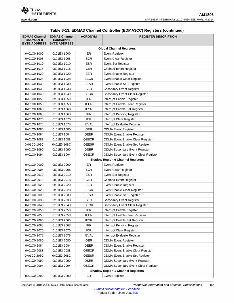
AM1806www.ti.com SPRS658F –FEBRUARY 2010–REVISED MARCH 2014
Table 6-13. EDMA3 Channel Controller (EDMA3CC) Registers (continued)EDMA0 Channel EDMA1 Channel ACRONYM REGISTER DESCRIPTION
Controller 0 Controller 0BYTE ADDRESS BYTE ADDRESS
Global Channel Registers0x01C0 1000 0x01E3 1000 ER Event Register0x01C0 1008 0x01E3 1008 ECR Event Clear Register0x01C0 1010 0x01E3 1010 ESR Event Set Register0x01C0 1018 0x01E3 1018 CER Chained Event Register0x01C0 1020 0x01E3 1020 EER Event Enable Register0x01C0 1028 0x01E3 1028 EECR Event Enable Clear Register0x01C0 1030 0x01E3 1030 EESR Event Enable Set Register0x01C0 1038 0x01E3 1038 SER Secondary Event Register0x01C0 1040 0x01E3 1040 SECR Secondary Event Clear Register0x01C0 1050 0x01E3 1050 IER Interrupt Enable Register0x01C0 1058 0x01E3 1058 IECR Interrupt Enable Clear Register0x01C0 1060 0x01E3 1060 IESR Interrupt Enable Set Register0x01C0 1068 0x01E3 1068 IPR Interrupt Pending Register0x01C0 1070 0x01E3 1070 ICR Interrupt Clear Register0x01C0 1078 0x01E3 1078 IEVAL Interrupt Evaluate Register0x01C0 1080 0x01E3 1080 QER QDMA Event Register0x01C0 1084 0x01E3 1084 QEER QDMA Event Enable Register0x01C0 1088 0x01E3 1088 QEECR QDMA Event Enable Clear Register0x01C0 108C 0x01E3 108C QEESR QDMA Event Enable Set Register0x01C0 1090 0x01E3 1090 QSER QDMA Secondary Event Register0x01C0 1094 0x01E3 1094 QSECR QDMA Secondary Event Clear Register
Shadow Region 0 Channel Registers0x01C0 2000 0x01E3 2000 ER Event Register0x01C0 2008 0x01E3 2008 ECR Event Clear Register0x01C0 2010 0x01E3 2010 ESR Event Set Register0x01C0 2018 0x01E3 2018 CER Chained Event Register0x01C0 2020 0x01E3 2020 EER Event Enable Register0x01C0 2028 0x01E3 2028 EECR Event Enable Clear Register0x01C0 2030 0x01E3 2030 EESR Event Enable Set Register0x01C0 2038 0x01E3 2038 SER Secondary Event Register0x01C0 2040 0x01E3 2040 SECR Secondary Event Clear Register0x01C0 2050 0x01E3 2050 IER Interrupt Enable Register0x01C0 2058 0x01E3 2058 IECR Interrupt Enable Clear Register0x01C0 2060 0x01E3 2060 IESR Interrupt Enable Set Register0x01C0 2068 0x01E3 2068 IPR Interrupt Pending Register0x01C0 2070 0x01E3 2070 ICR Interrupt Clear Register0x01C0 2078 0x01E3 2078 IEVAL Interrupt Evaluate Register0x01C0 2080 0x01E3 2080 QER QDMA Event Register0x01C0 2084 0x01E3 2084 QEER QDMA Event Enable Register0x01C0 2088 0x01E3 2088 QEECR QDMA Event Enable Clear Register0x01C0 208C 0x01E3 208C QEESR QDMA Event Enable Set Register0x01C0 2090 0x01E3 2090 QSER QDMA Secondary Event Register0x01C0 2094 0x01E3 2094 QSECR QDMA Secondary Event Clear Register
Shadow Region 1 Channel Registers0x01C0 2200 0x01E3 2200 ER Event Register
Copyright © 2010–2014, Texas Instruments Incorporated Peripheral Information and Electrical Specifications 89Submit Documentation Feedback
Product Folder Links: AM1806
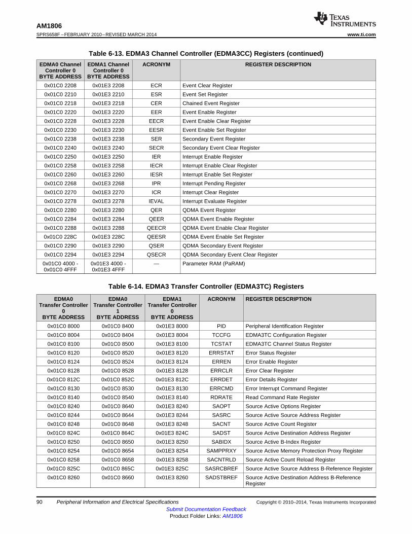
AM1806SPRS658F –FEBRUARY 2010–REVISED MARCH 2014 www.ti.com
Table 6-13. EDMA3 Channel Controller (EDMA3CC) Registers (continued)EDMA0 Channel EDMA1 Channel ACRONYM REGISTER DESCRIPTION
Controller 0 Controller 0BYTE ADDRESS BYTE ADDRESS
0x01C0 2208 0x01E3 2208 ECR Event Clear Register0x01C0 2210 0x01E3 2210 ESR Event Set Register0x01C0 2218 0x01E3 2218 CER Chained Event Register0x01C0 2220 0x01E3 2220 EER Event Enable Register0x01C0 2228 0x01E3 2228 EECR Event Enable Clear Register0x01C0 2230 0x01E3 2230 EESR Event Enable Set Register0x01C0 2238 0x01E3 2238 SER Secondary Event Register0x01C0 2240 0x01E3 2240 SECR Secondary Event Clear Register0x01C0 2250 0x01E3 2250 IER Interrupt Enable Register0x01C0 2258 0x01E3 2258 IECR Interrupt Enable Clear Register0x01C0 2260 0x01E3 2260 IESR Interrupt Enable Set Register0x01C0 2268 0x01E3 2268 IPR Interrupt Pending Register0x01C0 2270 0x01E3 2270 ICR Interrupt Clear Register0x01C0 2278 0x01E3 2278 IEVAL Interrupt Evaluate Register0x01C0 2280 0x01E3 2280 QER QDMA Event Register0x01C0 2284 0x01E3 2284 QEER QDMA Event Enable Register0x01C0 2288 0x01E3 2288 QEECR QDMA Event Enable Clear Register0x01C0 228C 0x01E3 228C QEESR QDMA Event Enable Set Register0x01C0 2290 0x01E3 2290 QSER QDMA Secondary Event Register0x01C0 2294 0x01E3 2294 QSECR QDMA Secondary Event Clear Register
0x01C0 4000 - 0x01E3 4000 - — Parameter RAM (PaRAM)0x01C0 4FFF 0x01E3 4FFF
Table 6-14. EDMA3 Transfer Controller (EDMA3TC) Registers
EDMA0 EDMA0 EDMA1 ACRONYM REGISTER DESCRIPTIONTransfer Controller Transfer Controller Transfer Controller
0 1 0BYTE ADDRESS BYTE ADDRESS BYTE ADDRESS
0x01C0 8000 0x01C0 8400 0x01E3 8000 PID Peripheral Identification Register0x01C0 8004 0x01C0 8404 0x01E3 8004 TCCFG EDMA3TC Configuration Register0x01C0 8100 0x01C0 8500 0x01E3 8100 TCSTAT EDMA3TC Channel Status Register0x01C0 8120 0x01C0 8520 0x01E3 8120 ERRSTAT Error Status Register0x01C0 8124 0x01C0 8524 0x01E3 8124 ERREN Error Enable Register0x01C0 8128 0x01C0 8528 0x01E3 8128 ERRCLR Error Clear Register0x01C0 812C 0x01C0 852C 0x01E3 812C ERRDET Error Details Register0x01C0 8130 0x01C0 8530 0x01E3 8130 ERRCMD Error Interrupt Command Register0x01C0 8140 0x01C0 8540 0x01E3 8140 RDRATE Read Command Rate Register0x01C0 8240 0x01C0 8640 0x01E3 8240 SAOPT Source Active Options Register0x01C0 8244 0x01C0 8644 0x01E3 8244 SASRC Source Active Source Address Register0x01C0 8248 0x01C0 8648 0x01E3 8248 SACNT Source Active Count Register0x01C0 824C 0x01C0 864C 0x01E3 824C SADST Source Active Destination Address Register0x01C0 8250 0x01C0 8650 0x01E3 8250 SABIDX Source Active B-Index Register0x01C0 8254 0x01C0 8654 0x01E3 8254 SAMPPRXY Source Active Memory Protection Proxy Register0x01C0 8258 0x01C0 8658 0x01E3 8258 SACNTRLD Source Active Count Reload Register0x01C0 825C 0x01C0 865C 0x01E3 825C SASRCBREF Source Active Source Address B-Reference Register0x01C0 8260 0x01C0 8660 0x01E3 8260 SADSTBREF Source Active Destination Address B-Reference
Register
90 Peripheral Information and Electrical Specifications Copyright © 2010–2014, Texas Instruments IncorporatedSubmit Documentation Feedback
Product Folder Links: AM1806
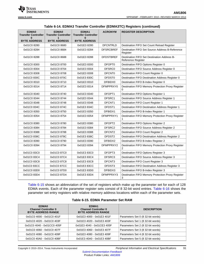
AM1806www.ti.com SPRS658F –FEBRUARY 2010–REVISED MARCH 2014
Table 6-14. EDMA3 Transfer Controller (EDMA3TC) Registers (continued)EDMA0 EDMA0 EDMA1 ACRONYM REGISTER DESCRIPTION
Transfer Controller Transfer Controller Transfer Controller0 1 0
BYTE ADDRESS BYTE ADDRESS BYTE ADDRESS0x01C0 8280 0x01C0 8680 0x01E3 8280 DFCNTRLD Destination FIFO Set Count Reload Register0x01C0 8284 0x01C0 8684 0x01E3 8284 DFSRCBREF Destination FIFO Set Source Address B-Reference
Register0x01C0 8288 0x01C0 8688 0x01E3 8288 DFDSTBREF Destination FIFO Set Destination Address B-
Reference Register0x01C0 8300 0x01C0 8700 0x01E3 8300 DFOPT0 Destination FIFO Options Register 00x01C0 8304 0x01C0 8704 0x01E3 8304 DFSRC0 Destination FIFO Source Address Register 00x01C0 8308 0x01C0 8708 0x01E3 8308 DFCNT0 Destination FIFO Count Register 00x01C0 830C 0x01C0 870C 0x01E3 830C DFDST0 Destination FIFO Destination Address Register 00x01C0 8310 0x01C0 8710 0x01E3 8310 DFBIDX0 Destination FIFO B-Index Register 00x01C0 8314 0x01C0 8714 0x01E3 8314 DFMPPRXY0 Destination FIFO Memory Protection Proxy Register
00x01C0 8340 0x01C0 8740 0x01E3 8340 DFOPT1 Destination FIFO Options Register 10x01C0 8344 0x01C0 8744 0x01E3 8344 DFSRC1 Destination FIFO Source Address Register 10x01C0 8348 0x01C0 8748 0x01E3 8348 DFCNT1 Destination FIFO Count Register 10x01C0 834C 0x01C0 874C 0x01E3 834C DFDST1 Destination FIFO Destination Address Register 10x01C0 8350 0x01C0 8750 0x01E3 8350 DFBIDX1 Destination FIFO B-Index Register 10x01C0 8354 0x01C0 8754 0x01E3 8354 DFMPPRXY1 Destination FIFO Memory Protection Proxy Register
10x01C0 8380 0x01C0 8780 0x01E3 8380 DFOPT2 Destination FIFO Options Register 20x01C0 8384 0x01C0 8784 0x01E3 8384 DFSRC2 Destination FIFO Source Address Register 20x01C0 8388 0x01C0 8788 0x01E3 8388 DFCNT2 Destination FIFO Count Register 20x01C0 838C 0x01C0 878C 0x01E3 838C DFDST2 Destination FIFO Destination Address Register 20x01C0 8390 0x01C0 8790 0x01E3 8390 DFBIDX2 Destination FIFO B-Index Register 20x01C0 8394 0x01C0 8794 0x01E3 8394 DFMPPRXY2 Destination FIFO Memory Protection Proxy Register
20x01C0 83C0 0x01C0 87C0 0x01E3 83C0 DFOPT3 Destination FIFO Options Register 30x01C0 83C4 0x01C0 87C4 0x01E3 83C4 DFSRC3 Destination FIFO Source Address Register 30x01C0 83C8 0x01C0 87C8 0x01E3 83C8 DFCNT3 Destination FIFO Count Register 30x01C0 83CC 0x01C0 87CC 0x01E3 83CC DFDST3 Destination FIFO Destination Address Register 30x01C0 83D0 0x01C0 87D0 0x01E3 83D0 DFBIDX3 Destination FIFO B-Index Register 30x01C0 83D4 0x01C0 87D4 0x01E3 83D4 DFMPPRXY3 Destination FIFO Memory Protection Proxy Register
3
Table 6-15 shows an abbreviation of the set of registers which make up the parameter set for each of 128EDMA events. Each of the parameter register sets consist of 8 32-bit word entries. Table 6-16 shows theparameter set entry registers with relative memory address locations within each of the parameter sets.
Table 6-15. EDMA Parameter Set RAM
EDMA0 EDMA1Channel Controller 0 Channel Controller 0 DESCRIPTION
BYTE ADDRESS RANGE BYTE ADDRESS RANGE0x01C0 4000 - 0x01C0 401F 0x01E3 4000 - 0x01E3 401F Parameters Set 0 (8 32-bit words)0x01C0 4020 - 0x01C0 403F 0x01E3 4020 - 0x01E3 403F Parameters Set 1 (8 32-bit words)
0x01C0 4040 - 0x01CC0 405F 0x01E3 4040 - 0x01CE3 405F Parameters Set 2 (8 32-bit words)0x01C0 4060 - 0x01C0 407F 0x01E3 4060 - 0x01E3 407F Parameters Set 3 (8 32-bit words)0x01C0 4080 - 0x01C0 409F 0x01E3 4080 - 0x01E3 409F Parameters Set 4 (8 32-bit words)0x01C0 40A0 - 0x01C0 40BF 0x01E3 40A0 - 0x01E3 40BF Parameters Set 5 (8 32-bit words)
Copyright © 2010–2014, Texas Instruments Incorporated Peripheral Information and Electrical Specifications 91Submit Documentation Feedback
Product Folder Links: AM1806
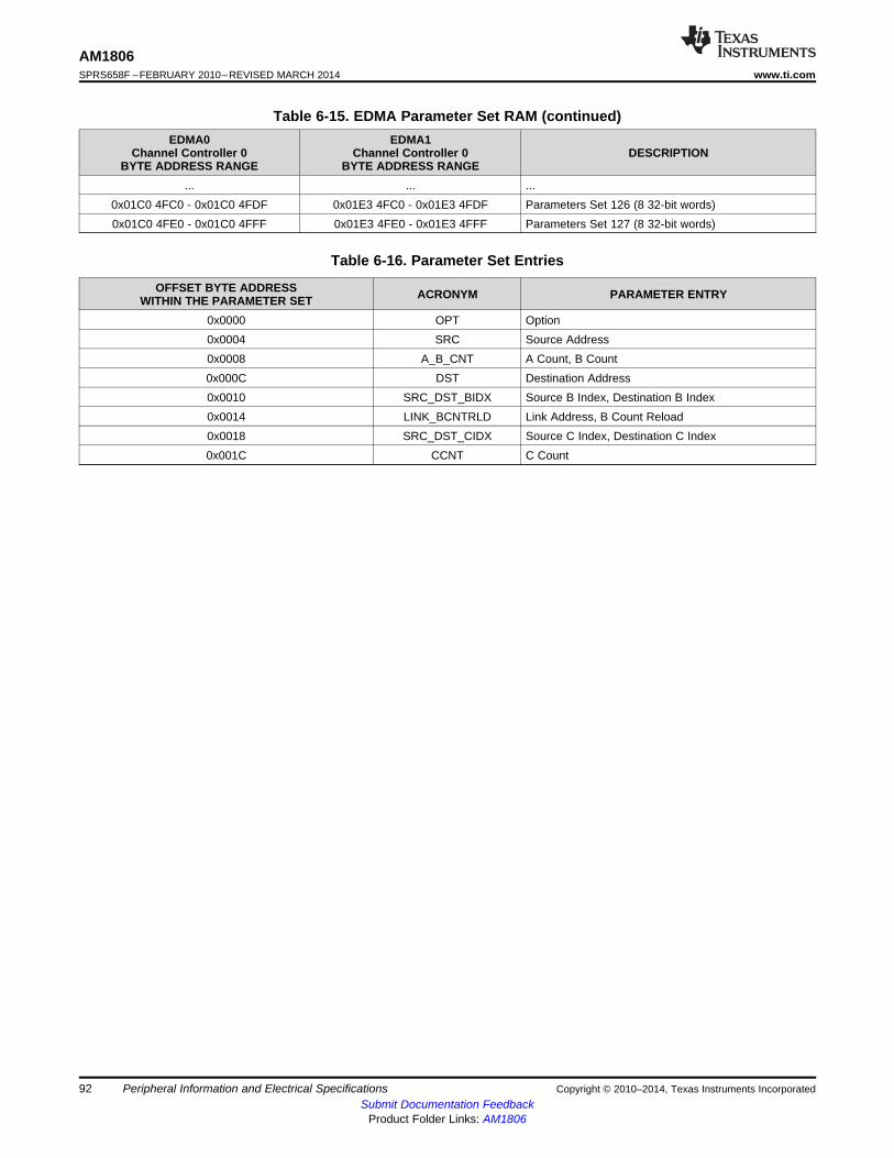
AM1806SPRS658F –FEBRUARY 2010–REVISED MARCH 2014 www.ti.com
Table 6-15. EDMA Parameter Set RAM (continued)EDMA0 EDMA1
Channel Controller 0 Channel Controller 0 DESCRIPTIONBYTE ADDRESS RANGE BYTE ADDRESS RANGE
... ... ...0x01C0 4FC0 - 0x01C0 4FDF 0x01E3 4FC0 - 0x01E3 4FDF Parameters Set 126 (8 32-bit words)0x01C0 4FE0 - 0x01C0 4FFF 0x01E3 4FE0 - 0x01E3 4FFF Parameters Set 127 (8 32-bit words)
Table 6-16. Parameter Set Entries
OFFSET BYTE ADDRESS ACRONYM PARAMETER ENTRYWITHIN THE PARAMETER SET0x0000 OPT Option0x0004 SRC Source Address0x0008 A_B_CNT A Count, B Count0x000C DST Destination Address0x0010 SRC_DST_BIDX Source B Index, Destination B Index0x0014 LINK_BCNTRLD Link Address, B Count Reload0x0018 SRC_DST_CIDX Source C Index, Destination C Index0x001C CCNT C Count
92 Peripheral Information and Electrical Specifications Copyright © 2010–2014, Texas Instruments IncorporatedSubmit Documentation Feedback
Product Folder Links: AM1806
AM1806www.ti.com SPRS658F –FEBRUARY 2010–REVISED MARCH 2014
6.10 External Memory Interface A (EMIFA)EMIFA is one of two external memory interfaces supported on the device. It is primarily intended tosupport asynchronous memory types, such as NAND and NOR flash and Asynchronous SRAM. Howeveron this device, EMIFA also provides a secondary interface to SDRAM.
6.10.1 EMIFA Asynchronous Memory SupportEMIFA supports asynchronous:• SRAM memories• NAND Flash memories• NOR Flash memories
The EMIFA data bus width is up to 16-bits.The device supports up to 23 address lines and two externalwait/interrupt inputs. Up to four asynchronous chip selects are supported by EMIFA (EMA_CS[5:2]).
Each chip select has the following individually programmable attributes:• Data Bus Width• Read cycle timings: setup, hold, strobe• Write cycle timings: setup, hold, strobe• Bus turn around time• Extended Wait Option With Programmable Timeout• Select Strobe Option• NAND flash controller supports 1-bit and 4-bit ECC calculation on blocks of 512 bytes.
6.10.2 EMIFA Synchronous DRAM Memory SupportThe device supports 16-bit SDRAM in addition to the asynchronous memories listed in Section 6.10.1. Ithas a single SDRAM chip select (EMA_CS[0]). SDRAM configurations that are supported are:• One, Two, and Four Bank SDRAM devices• Devices with Eight, Nine, Ten, and Eleven Column Address• CAS Latency of two or three clock cycles• Sixteen Bit Data Bus Width
Additionally, the SDRAM interface of EMIFA supports placing the SDRAM in Self Refresh and PowerdownModes. Self Refresh mode allows the SDRAM to be put into a low power state while still retaining memorycontents; since the SDRAM will continue to refresh itself even without clocks from the device. Powerdownmode achieves even lower power, except the device must periodically wake the SDRAM up and issuerefreshes if data retention is required.
Finally, note that the EMIFA does not support Mobile SDRAM devices.
Table 6-17 shows the supported SDRAM configurations for EMIFA.
Copyright © 2010–2014, Texas Instruments Incorporated Peripheral Information and Electrical Specifications 93Submit Documentation Feedback
Product Folder Links: AM1806
AM1806SPRS658F –FEBRUARY 2010–REVISED MARCH 2014 www.ti.com
Table 6-17. EMIFA Supported SDRAM Configurations (1)
SDRAM EMIFA Data Total Total MemoryMemory Number of Bus Size Rows Columns Banks Memory Memory DensityData Bus Memories (bits) (Mbits) (Mbytes) (Mbits)Width (bits)1 16 16 8 1 256 32 2561 16 16 8 2 512 64 5121 16 16 8 4 1024 128 10241 16 16 9 1 512 64 5121 16 16 9 2 1024 128 1024
16 1 16 16 9 4 2048 256 20481 16 16 10 1 1024 128 10241 16 16 10 2 2048 256 20481 16 16 10 4 4096 512 40961 16 16 11 1 2048 256 20481 16 16 11 2 4096 512 40961 16 15 11 4 4096 512 40962 16 16 8 1 256 32 1282 16 16 8 2 512 64 2562 16 16 8 4 1024 128 5122 16 16 9 1 512 64 2562 16 16 9 2 1024 128 512
8 2 16 16 9 4 2048 256 10242 16 16 10 1 1024 128 5122 16 16 10 2 2048 256 10242 16 16 10 4 4096 512 20482 16 16 11 1 2048 256 10242 16 16 11 2 4096 512 20482 16 15 11 4 4096 512 2048
(1) The shaded cells indicate configurations that are possible on the EMIFA interface but as of this writing SDRAM memories capable ofsupporting these densities are not available in the market.
6.10.3 EMIFA SDRAM Loading LimitationsEMIFA supports SDRAM up to 100 MHz with up to two SDRAM or asynchronous memory loads.Additional loads will limit the SDRAM operation to lower speeds and the maximum speed should beconfirmed by board simulation using IBIS models.
94 Peripheral Information and Electrical Specifications Copyright © 2010–2014, Texas Instruments IncorporatedSubmit Documentation Feedback
Product Folder Links: AM1806
AM1806www.ti.com SPRS658F –FEBRUARY 2010–REVISED MARCH 2014
6.10.4 External Memory Interface Register Descriptions
Table 6-18. External Memory Interface (EMIFA) Registers
BYTE ADDRESS ACRONYM REGISTER DESCRIPTION0x6800 0000 MIDR Module ID Register0x6800 0004 AWCC Asynchronous Wait Cycle Configuration Register0x6800 0008 SDCR SDRAM Configuration Register0x6800 000C SDRCR SDRAM Refresh Control Register0x6800 0010 CE2CFG Asynchronous 1 Configuration Register0x6800 0014 CE3CFG Asynchronous 2 Configuration Register0x6800 0018 CE4CFG Asynchronous 3 Configuration Register0x6800 001C CE5CFG Asynchronous 4 Configuration Register0x6800 0020 SDTIMR SDRAM Timing Register0x6800 003C SDSRETR SDRAM Self Refresh Exit Timing Register0x6800 0040 INTRAW EMIFA Interrupt Raw Register0x6800 0044 INTMSK EMIFA Interrupt Mask Register0x6800 0048 INTMSKSET EMIFA Interrupt Mask Set Register0x6800 004C INTMSKCLR EMIFA Interrupt Mask Clear Register0x6800 0060 NANDFCR NAND Flash Control Register0x6800 0064 NANDFSR NAND Flash Status Register0x6800 0070 NANDF1ECC NAND Flash 1 ECC Register (CS2 Space)0x6800 0074 NANDF2ECC NAND Flash 2 ECC Register (CS3 Space)0x6800 0078 NANDF3ECC NAND Flash 3 ECC Register (CS4 Space)0x6800 007C NANDF4ECC NAND Flash 4 ECC Register (CS5 Space)0x6800 00BC NAND4BITECCLOAD NAND Flash 4-Bit ECC Load Register0x6800 00C0 NAND4BITECC1 NAND Flash 4-Bit ECC Register 10x6800 00C4 NAND4BITECC2 NAND Flash 4-Bit ECC Register 20x6800 00C8 NAND4BITECC3 NAND Flash 4-Bit ECC Register 30x6800 00CC NAND4BITECC4 NAND Flash 4-Bit ECC Register 40x6800 00D0 NANDERRADD1 NAND Flash 4-Bit ECC Error Address Register 10x6800 00D4 NANDERRADD2 NAND Flash 4-Bit ECC Error Address Register 20x6800 00D8 NANDERRVAL1 NAND Flash 4-Bit ECC Error Value Register 10x6800 00DC NANDERRVAL2 NAND Flash 4-Bit ECC Error Value Register 2
Copyright © 2010–2014, Texas Instruments Incorporated Peripheral Information and Electrical Specifications 95Submit Documentation Feedback
Product Folder Links: AM1806
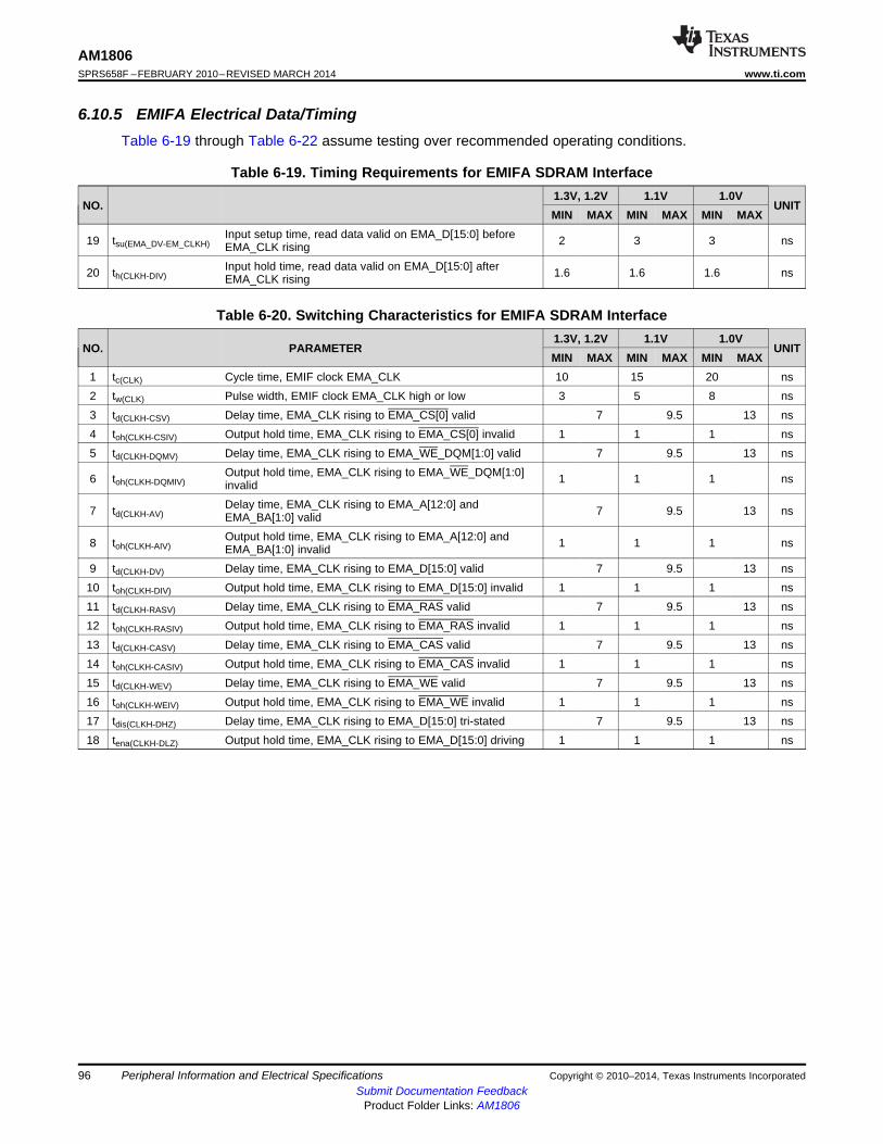
AM1806SPRS658F –FEBRUARY 2010–REVISED MARCH 2014 www.ti.com
6.10.5 EMIFA Electrical Data/TimingTable 6-19 through Table 6-22 assume testing over recommended operating conditions.
Table 6-19. Timing Requirements for EMIFA SDRAM Interface1.3V, 1.2V 1.1V 1.0V
NO. UNITMIN MAX MIN MAX MIN MAX
Input setup time, read data valid on EMA_D[15:0] before19 tsu(EMA_DV-EM_CLKH) 2 3 3 nsEMA_CLK risingInput hold time, read data valid on EMA_D[15:0] after20 th(CLKH-DIV) 1.6 1.6 1.6 nsEMA_CLK rising
Table 6-20. Switching Characteristics for EMIFA SDRAM Interface1.3V, 1.2V 1.1V 1.0V
NO. PARAMETER UNITMIN MAX MIN MAX MIN MAX
1 tc(CLK) Cycle time, EMIF clock EMA_CLK 10 15 20 ns2 tw(CLK) Pulse width, EMIF clock EMA_CLK high or low 3 5 8 ns3 td(CLKH-CSV) Delay time, EMA_CLK rising to EMA_CS[0] valid 7 9.5 13 ns4 toh(CLKH-CSIV) Output hold time, EMA_CLK rising to EMA_CS[0] invalid 1 1 1 ns5 td(CLKH-DQMV) Delay time, EMA_CLK rising to EMA_WE_DQM[1:0] valid 7 9.5 13 ns
Output hold time, EMA_CLK rising to EMA_WE_DQM[1:0]6 toh(CLKH-DQMIV) 1 1 1 nsinvalidDelay time, EMA_CLK rising to EMA_A[12:0] and7 td(CLKH-AV) 7 9.5 13 nsEMA_BA[1:0] validOutput hold time, EMA_CLK rising to EMA_A[12:0] and8 toh(CLKH-AIV) 1 1 1 nsEMA_BA[1:0] invalid
9 td(CLKH-DV) Delay time, EMA_CLK rising to EMA_D[15:0] valid 7 9.5 13 ns10 toh(CLKH-DIV) Output hold time, EMA_CLK rising to EMA_D[15:0] invalid 1 1 1 ns11 td(CLKH-RASV) Delay time, EMA_CLK rising to EMA_RAS valid 7 9.5 13 ns12 toh(CLKH-RASIV) Output hold time, EMA_CLK rising to EMA_RAS invalid 1 1 1 ns13 td(CLKH-CASV) Delay time, EMA_CLK rising to EMA_CAS valid 7 9.5 13 ns14 toh(CLKH-CASIV) Output hold time, EMA_CLK rising to EMA_CAS invalid 1 1 1 ns15 td(CLKH-WEV) Delay time, EMA_CLK rising to EMA_WE valid 7 9.5 13 ns16 toh(CLKH-WEIV) Output hold time, EMA_CLK rising to EMA_WE invalid 1 1 1 ns17 tdis(CLKH-DHZ) Delay time, EMA_CLK rising to EMA_D[15:0] tri-stated 7 9.5 13 ns18 tena(CLKH-DLZ) Output hold time, EMA_CLK rising to EMA_D[15:0] driving 1 1 1 ns
96 Peripheral Information and Electrical Specifications Copyright © 2010–2014, Texas Instruments IncorporatedSubmit Documentation Feedback
Product Folder Links: AM1806
EMA_CLK
EMA_BA[1:0]
EMA_A[12:0]
EMA_D[15:0]
1
2 2
4
6
8
8
12
14
19
20
3
5
7
7
11
13
17 182 EM_CLK Delay
BASIC SDRAMREAD OPERATION
EMA_CS[0]
EMA_WE_DQM[1:0]
EMA_RAS
EMA_CAS
EMA_WE
EMA_CLK
EMA_BA[1:0]
EMA_A[12:0]
EMA_D[15:0]
1
2 2
4
6
8
8
12
10
16
3
5
7
7
11
13
15
9
BASIC SDRAMWRITE OPERATION
EMA_CS[0]
EMA_WE_DQM[1:0]
EMA_RAS
EMA_CAS
EMA_WE
AM1806www.ti.com SPRS658F –FEBRUARY 2010–REVISED MARCH 2014
Figure 6-10. EMIFA Basic SDRAM Write Operation
Figure 6-11. EMIFA Basic SDRAM Read Operation
Copyright © 2010–2014, Texas Instruments Incorporated Peripheral Information and Electrical Specifications 97Submit Documentation Feedback
Product Folder Links: AM1806
AM1806SPRS658F –FEBRUARY 2010–REVISED MARCH 2014 www.ti.com
Table 6-21. Timing Requirements for EMIFA Asynchronous Memory Interface (1)
1.2V 1.1V 1.0VNO. UNIT
MIN MAX MIN MAX MIN MAXREADS and WRITES
E tc(CLK) Cycle time, EMIFA module clock 6.75 13.33 20 ns2 tw(EM_WAIT) Pulse duration, EM_WAIT assertion and deassertion 2E 2E 2E ns
READS12 tsu(EMDV-EMOEH) Setup time, EM_D[15:0] valid before EM_OE high 3 5 7 ns13 th(EMOEH-EMDIV) Hold time, EM_D[15:0] valid after EM_OE high 0 0 0 ns
tsu (EMOEL- Setup Time, EM_WAIT asserted before end of Strobe14 4E+3 4E+3 4E+3 nsEMWAIT) Phase
WRITEStsu (EMWEL- Setup Time, EM_WAIT asserted before end of Strobe28 4E+3 4E+3 4E+3 nsEMWAIT) Phase
(1) E = EMA_CLK period or in ns. EMA_CLK is selected either as SYSCLK3 or the PLL0 output clock divided by 4.5. As an example, whenSYSCLK3 is selected and set to 100MHz, E=10ns
98 Peripheral Information and Electrical Specifications Copyright © 2010–2014, Texas Instruments IncorporatedSubmit Documentation Feedback
Product Folder Links: AM1806
AM1806www.ti.com SPRS658F –FEBRUARY 2010–REVISED MARCH 2014
Table 6-22. Switching Characteristics for EMIFA Asynchronous Memory Interface (1) (2) (3)
1.3V, 1.2V, 1.1V, 1.0VNO. PARAMETER UNIT
MIN Nom MAX
READS and WRITES
1 td(TURNAROUND) Turn around time (TA)*E - 3 (TA)*E (TA)*E + 3 ns
READS
EMIF read cycle time (EW = 0) (RS+RST+RH)*E - 3 (RS+RST+RH)*E (RS+RST+RH)*E + 3 ns3 tc(EMRCYCLE)
EMIF read cycle time (EW = 1) (RS+RST+RH+EWC)*E - 3 (RS+RST+RH+EWC)*E (RS+RST+RH+EWC)*E + 3 ns
Output setup time, EMA_CE[5:2] low to EMA_OE low (SS = 0) (RS)*E-3 (RS)*E (RS)*E+3 ns4 tsu(EMCEL-EMOEL)
Output setup time, EMA_CE[5:2] low to EMA_OE low (SS = 1) -3 0 +3 ns
Output hold time, EMA_OE high to EMA_CE[5:2] high (SS = 0) (RH)*E - 3 (RH)*E (RH)*E + 3 ns5 th(EMOEH-EMCEH)
Output hold time, EMA_OE high to EMA_CE[5:2] high (SS = 1) -3 0 +3 ns
6 tsu(EMBAV-EMOEL) Output setup time, EMA_BA[1:0] valid to EMA_OE low (RS)*E-3 (RS)*E (RS)*E+3 ns
7 th(EMOEH-EMBAIV) Output hold time, EMA_OE high to EMA_BA[1:0] invalid (RH)*E-3 (RH)*E (RH)*E+3 ns
8 tsu(EMBAV-EMOEL) Output setup time, EMA_A[13:0] valid to EMA_OE low (RS)*E-3 (RS)*E (RS)*E+3 ns
9 th(EMOEH-EMAIV) Output hold time, EMA_OE high to EMA_A[13:0] invalid (RH)*E-3 (RH)*E (RH)*E+3 ns
EMA_OE active low width (EW = 0) (RST)*E-3 (RST)*E (RST)*E+3 ns10 tw(EMOEL)
EMA_OE active low width (EW = 1) (RST+EWC)*E-3 (RST+EWC)*E (RST+EWC)*E+3 ns
11 td(EMWAITH-EMOEH) Delay time from EMA_WAIT deasserted to EMA_OE high 3E-3 4E 4E+3 ns
28 tsu(EMARW-EMOEL) Output setup time, EMA_A_RW valid to EMA_OE low (RS)*E-3 (RS)*E (RS)*E+3 ns
29 th(EMOEH-EMARW) Output hold time, EMA_OE high to EMA_A_RW invalid (RH)*E-3 (RH)*E (RH)*E+3 ns
WRITES
EMIF write cycle time (EW = 0) (WS+WST+WH)*E-3 (WS+WST+WH)*E (WS+WST+WH)*E+3 ns15 tc(EMWCYCLE) (WS+WST+WH+EWC)*E +EMIF write cycle time (EW = 1) (WS+WST+WH+EWC)*E - 3 (WS+WST+WH+EWC)*E ns3
Output setup time, EMA_CE[5:2] low to EMA_WE low (SS = 0) (WS)*E - 3 (WS)*E (WS)*E + 3 ns16 tsu(EMCEL-EMWEL)
Output setup time, EMA_CE[5:2] low to EMA_WE low (SS = 1) -3 0 +3 ns
Output hold time, EMA_WE high to EMA_CE[5:2] high (SS = 0) (WH)*E-3 (WH)*E (WH)*E+3 ns17 th(EMWEH-EMCEH)
Output hold time, EMA_WE high to EMA_CE[5:2] high (SS = 1) -3 0 +3 ns
18 tsu(EMDQMV-EMWEL) Output setup time, EMA_BA[1:0] valid to EMA_WE low (WS)*E-3 (WS)*E (WS)*E+3 ns
19 th(EMWEH-EMDQMIV) Output hold time, EMA_WE high to EMA_BA[1:0] invalid (WH)*E-3 (WH)*E (WH)*E+3 ns
20 tsu(EMBAV-EMWEL) Output setup time, EMA_BA[1:0] valid to EMA_WE low (WS)*E-3 (WS)*E (WS)*E+3 ns
21 th(EMWEH-EMBAIV) Output hold time, EMA_WE high to EMA_BA[1:0] invalid (WH)*E-3 (WH)*E (WH)*E+3 ns
(1) TA = Turn around, RS = Read setup, RST = Read strobe, RH = Read hold, WS = Write setup, WST = Write strobe, WH = Write hold, MEWC = Maximum external wait cycles. Theseparameters are programmed via the Asynchronous Bank and Asynchronous Wait Cycle Configuration Registers. These support the following range of values: TA[4-1], RS[16-1], RST[64-1], RH[8-1], WS[16-1], WST[64-1], WH[8-1], and MEW[1-256].
(2) E = EMA_CLK period or in ns. EMA_CLK is selected either as SYSCLK3 or the PLL0 output clock divided by 4.5. As an example, when SYSCLK3 is selected and set to 100MHz,E=10ns.
(3) EWC = external wait cycles determined by EMA_WAIT input signal. EWC supports the following range of values EWC[256-1]. Note that the maximum wait time before timeout is specifiedby bit field MEWC in the Asynchronous Wait Cycle Configuration Register.
Copyright © 2010–2014, Texas Instruments Incorporated Peripheral Information and Electrical Specifications 99Submit Documentation Feedback
Product Folder Links: AM1806
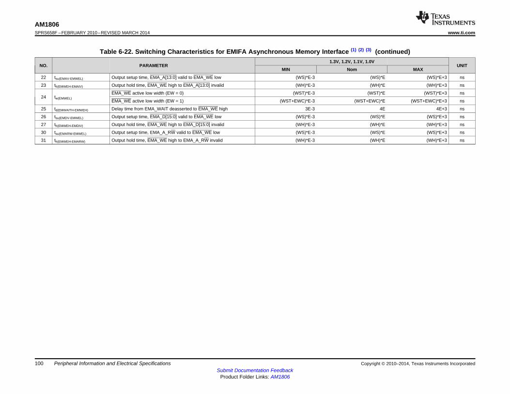
AM1806SPRS658F –FEBRUARY 2010–REVISED MARCH 2014 www.ti.com
Table 6-22. Switching Characteristics for EMIFA Asynchronous Memory Interface (1) (2) (3) (continued)1.3V, 1.2V, 1.1V, 1.0V
NO. PARAMETER UNITMIN Nom MAX
22 tsu(EMAV-EMWEL) Output setup time, EMA_A[13:0] valid to EMA_WE low (WS)*E-3 (WS)*E (WS)*E+3 ns
23 th(EMWEH-EMAIV) Output hold time, EMA_WE high to EMA_A[13:0] invalid (WH)*E-3 (WH)*E (WH)*E+3 ns
EMA_WE active low width (EW = 0) (WST)*E-3 (WST)*E (WST)*E+3 ns24 tw(EMWEL)
EMA_WE active low width (EW = 1) (WST+EWC)*E-3 (WST+EWC)*E (WST+EWC)*E+3 ns
25 td(EMWAITH-EMWEH) Delay time from EMA_WAIT deasserted to EMA_WE high 3E-3 4E 4E+3 ns
26 tsu(EMDV-EMWEL) Output setup time, EMA_D[15:0] valid to EMA_WE low (WS)*E-3 (WS)*E (WS)*E+3 ns
27 th(EMWEH-EMDIV) Output hold time, EMA_WE high to EMA_D[15:0] invalid (WH)*E-3 (WH)*E (WH)*E+3 ns
30 tsu(EMARW-EMWEL) Output setup time, EMA_A_RW valid to EMA_WE low (WS)*E-3 (WS)*E (WS)*E+3 ns
31 th(EMWEH-EMARW) Output hold time, EMA_WE high to EMA_A_RW invalid (WH)*E-3 (WH)*E (WH)*E+3 ns
100 Peripheral Information and Electrical Specifications Copyright © 2010–2014, Texas Instruments IncorporatedSubmit Documentation Feedback
Product Folder Links: AM1806
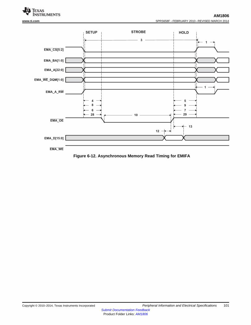
EMA_CS[5:2]
EMA_BA[1:0]
13
12
EMA_A[22:0]
EMA_OE
EMA_D[15:0]
EMA_WE
10
5
9
7
4
8
31
EMA_ _DQM[1:0]WE
EMA_A_RW
1
6
28 29
SETUP STROBE HOLD
AM1806www.ti.com SPRS658F –FEBRUARY 2010–REVISED MARCH 2014
Figure 6-12. Asynchronous Memory Read Timing for EMIFA
Copyright © 2010–2014, Texas Instruments Incorporated Peripheral Information and Electrical Specifications 101Submit Documentation Feedback
Product Folder Links: AM1806
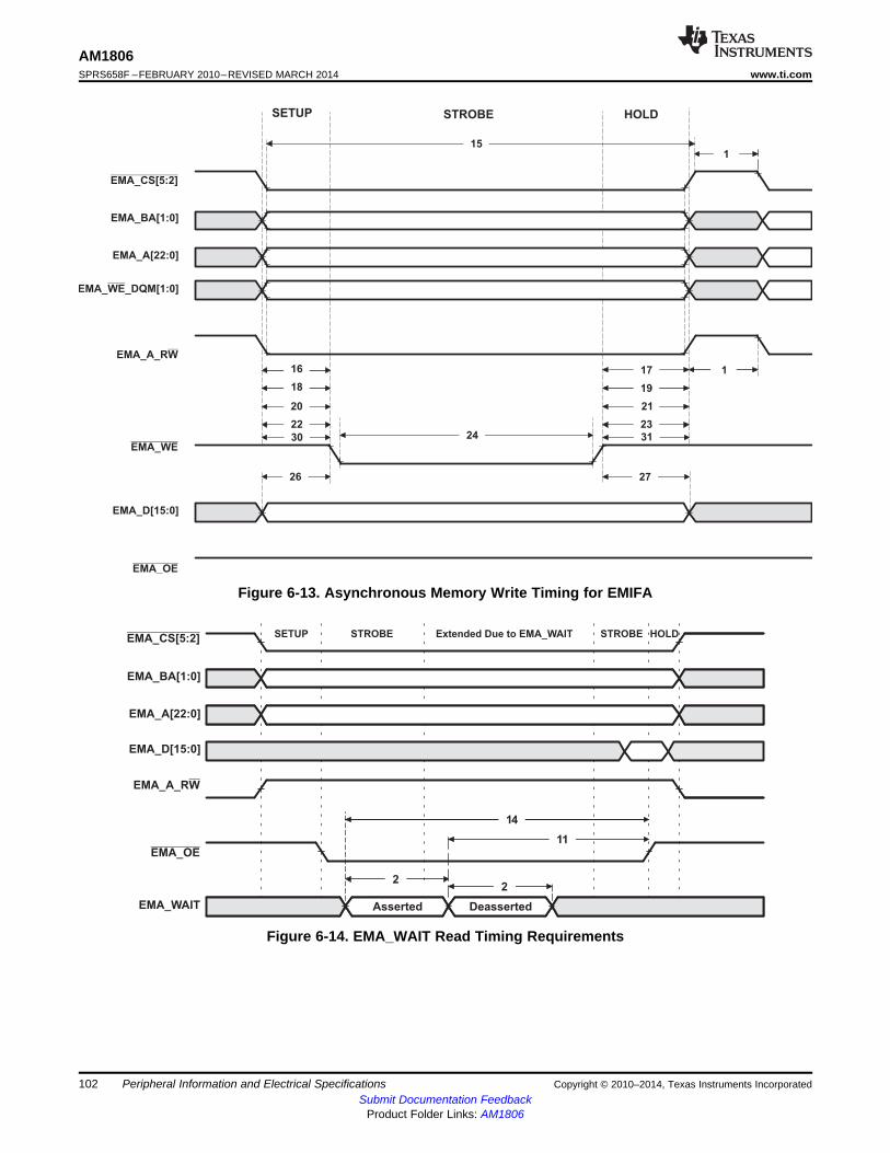
EMA_CS[5:2]
11
Asserted Deasserted
22
EMA_BA[1:0]
EMA_A[22:0]
EMA_D[15:0]
EMA_OE
EMA_WAIT
SETUP STROBE Extended Due to EMA_WAIT STROBE HOLD
14
EMA_A_RW
EMA_CS[5:2]
EMA_BA[1:0]
EMA_A[22:0]
EMA_WE
EMA_D[15:0]
EMA_OE
151
16
18
20
2224
17
19
21
23
26 27
EMA_ _DQM[1:0]WE
EMA_A_RW
1
30 31
SETUP STROBE HOLD
AM1806SPRS658F –FEBRUARY 2010–REVISED MARCH 2014 www.ti.com
Figure 6-13. Asynchronous Memory Write Timing for EMIFA
Figure 6-14. EMA_WAIT Read Timing Requirements
102 Peripheral Information and Electrical Specifications Copyright © 2010–2014, Texas Instruments IncorporatedSubmit Documentation Feedback
Product Folder Links: AM1806
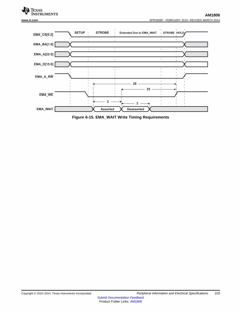
EMA_A[22:0]
EMA_CS[5:2]
EMA_BA[1:0]
EMA_D[15:0]
EMA_A_RW
EMA_WE
EMA_WAIT
AM1806www.ti.com SPRS658F –FEBRUARY 2010–REVISED MARCH 2014
Figure 6-15. EMA_WAIT Write Timing Requirements
Copyright © 2010–2014, Texas Instruments Incorporated Peripheral Information and Electrical Specifications 103Submit Documentation Feedback
Product Folder Links: AM1806
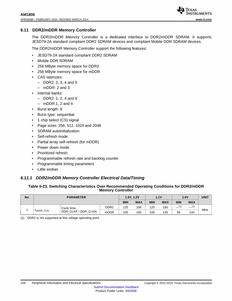
AM1806SPRS658F –FEBRUARY 2010–REVISED MARCH 2014 www.ti.com
6.11 DDR2/mDDR Memory ControllerThe DDR2/mDDR Memory Controller is a dedicated interface to DDR2/mDDR SDRAM. It supportsJESD79-2A standard compliant DDR2 SDRAM devices and compliant Mobile DDR SDRAM devices.
The DDR2/mDDR Memory Controller support the following features:
• JESD79-2A standard compliant DDR2 SDRAM• Mobile DDR SDRAM• 256 MByte memory space for DDR2• 256 MByte memory space for mDDR• CAS latencies:
– DDR2: 2, 3, 4 and 5– mDDR: 2 and 3
• Internal banks:– DDR2: 1, 2, 4 and 8– mDDR:1, 2 and 4
• Burst length: 8• Burst type: sequential• 1 chip select (CS) signal• Page sizes: 256, 512, 1024 and 2048• SDRAM autoinitialization• Self-refresh mode• Partial array self-refresh (for mDDR)• Power down mode• Prioritized refresh• Programmable refresh rate and backlog counter• Programmable timing parameters• Little endian
6.11.1 DDR2/mDDR Memory Controller Electrical Data/Timing
Table 6-23. Switching Characteristics Over Recommended Operating Conditions for DDR2/mDDRMemory Controller
No. PARAMETER 1.3V, 1.2V 1.1V 1.0V UNITMIN MAX MIN MAX MIN MAX
DDR2 125 156 125 150 — (1) — (1)Cycle time,1 tc(DDR_CLK) MHzDDR_CLKP / DDR_CLKN mDDR 105 150 100 133 95 133
(1) DDR2 is not supported at this voltage operating point.
104 Peripheral Information and Electrical Specifications Copyright © 2010–2014, Texas Instruments IncorporatedSubmit Documentation Feedback
Product Folder Links: AM1806
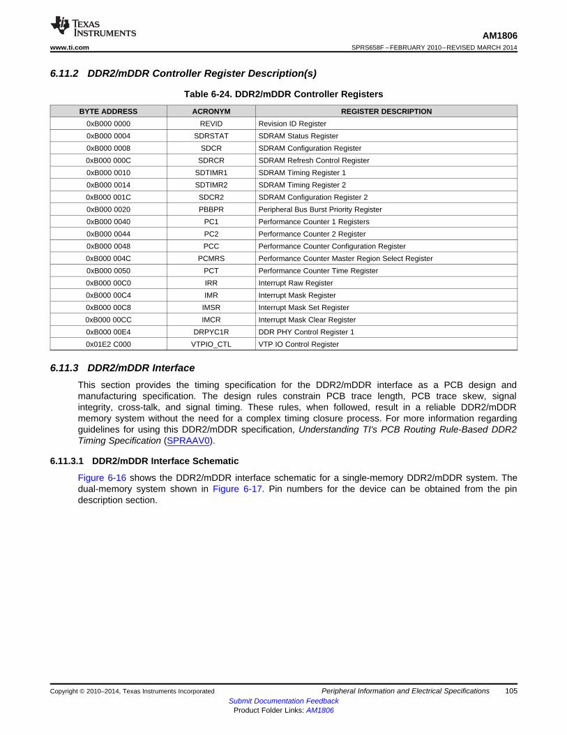
AM1806www.ti.com SPRS658F –FEBRUARY 2010–REVISED MARCH 2014
6.11.2 DDR2/mDDR Controller Register Description(s)
Table 6-24. DDR2/mDDR Controller Registers
BYTE ADDRESS ACRONYM REGISTER DESCRIPTION0xB000 0000 REVID Revision ID Register0xB000 0004 SDRSTAT SDRAM Status Register0xB000 0008 SDCR SDRAM Configuration Register0xB000 000C SDRCR SDRAM Refresh Control Register0xB000 0010 SDTIMR1 SDRAM Timing Register 10xB000 0014 SDTIMR2 SDRAM Timing Register 20xB000 001C SDCR2 SDRAM Configuration Register 20xB000 0020 PBBPR Peripheral Bus Burst Priority Register0xB000 0040 PC1 Performance Counter 1 Registers0xB000 0044 PC2 Performance Counter 2 Register0xB000 0048 PCC Performance Counter Configuration Register0xB000 004C PCMRS Performance Counter Master Region Select Register0xB000 0050 PCT Performance Counter Time Register0xB000 00C0 IRR Interrupt Raw Register0xB000 00C4 IMR Interrupt Mask Register0xB000 00C8 IMSR Interrupt Mask Set Register0xB000 00CC IMCR Interrupt Mask Clear Register0xB000 00E4 DRPYC1R DDR PHY Control Register 10x01E2 C000 VTPIO_CTL VTP IO Control Register
6.11.3 DDR2/mDDR InterfaceThis section provides the timing specification for the DDR2/mDDR interface as a PCB design andmanufacturing specification. The design rules constrain PCB trace length, PCB trace skew, signalintegrity, cross-talk, and signal timing. These rules, when followed, result in a reliable DDR2/mDDRmemory system without the need for a complex timing closure process. For more information regardingguidelines for using this DDR2/mDDR specification, Understanding TI's PCB Routing Rule-Based DDR2Timing Specification (SPRAAV0).
6.11.3.1 DDR2/mDDR Interface Schematic
Figure 6-16 shows the DDR2/mDDR interface schematic for a single-memory DDR2/mDDR system. Thedual-memory system shown in Figure 6-17. Pin numbers for the device can be obtained from the pindescription section.
Copyright © 2010–2014, Texas Instruments Incorporated Peripheral Information and Electrical Specifications 105Submit Documentation Feedback
Product Folder Links: AM1806
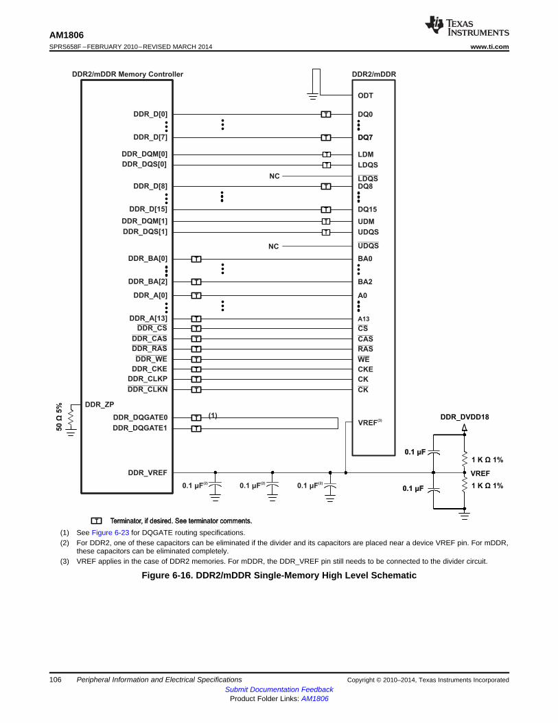
DDR2/mDDR Memory Controller
DDR_D[7]
DDR2/mDDR
DDR_DQM[0]
ODT
DQ0
DQ7
DDR_D[8]
DDR_D[15]
DQ8
DQ15
LDM
LDQS
LDQS
DDR_DQM[1]
DDR_DQS[1]
UDM
UDQS
UDQS
DDR_BA[0]
DDR_BA[2]
BA0
BA2
DDR_A[0]
DDR_A[13]
A0
DDR_CS
DDR_CAS
CS
CAS
DDR_RAS
DDR_WE
RAS
WE
DDR_CKE CKE
DDR_CLKP
DDR_CLKN
CK
CK
DDR_DQGATE0
DDR_DQGATE1
DDR_ZP
DDR_VREF
1 K Ω 1%
DDR_DVDD18
VREF
1 K Ω 1%0.1 μF
0.1 μF
0.1 Fμ(2)
0.1 Fμ(2)
50
5Ω
%
T Terminator, if desired. See terminator comments.
DQ7
A13
0.1 μF
0.1 μF
T Terminator, if desired. See terminator comments.
DDR_D[0]
NC
TTT
TTT
TTT
TTT
TTT
TTT
TTT
TTT
TTT
TTT
TTT
TTT
TTT
TTT
TTT
TTT
TTT
TTT
TTT
T
T
T
T
T
TVREF
(3)
T Terminator, if desired. See terminator comments.
0.1 Fμ(2)
DDR_DQS[0]
NC
(1)
AM1806SPRS658F –FEBRUARY 2010–REVISED MARCH 2014 www.ti.com
(1) See Figure 6-23 for DQGATE routing specifications.(2) For DDR2, one of these capacitors can be eliminated if the divider and its capacitors are placed near a device VREF pin. For mDDR,
these capacitors can be eliminated completely.(3) VREF applies in the case of DDR2 memories. For mDDR, the DDR_VREF pin still needs to be connected to the divider circuit.
Figure 6-16. DDR2/mDDR Single-Memory High Level Schematic
106 Peripheral Information and Electrical Specifications Copyright © 2010–2014, Texas Instruments IncorporatedSubmit Documentation Feedback
Product Folder Links: AM1806
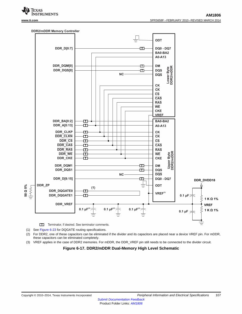
DDR2/mDDR Memory Controller
DDR_D[0:7]
Lo
wer
Byte
DD
R2/m
DD
RDDR_DQM[0]
DDR_DQS[0]
ODT
DQ0 - DQ7
BA0-BA2
CK
CK
DM
DQS
DQS
CS
CAS
RAS
DDR_BA[0:2]
CKE
BA0-BA2
DDR_A[0:13]
DDR_CLKP
A0-A13
DDR_CLKN
DDR_CS
CK
CS
DDR_CAS
DDR_RAS
CAS
RAS
DDR_WE WE
DDR_D[8:15]
DQS
DQ0 - DQ7
DDR_DQGATE0
DDR_DQGATE1
T
T
T
T
T
T
T
T
T
T
T
T
T
T
DDR_ZP
VREF(3)
DDR_VREF
1 K Ω 1%
DDR_DVDD18
VREF
1 K Ω 1%0.1 μF
0.1 μF
0.1 μF(2)
0.1 μF(2)
0.1 μF(2)
50
5Ω
%
T Terminator, if desired. See terminator comments.
ODT
A0-A13
WE
VREF
Up
per
Byte
DD
R2/m
DD
R
CK
DDR_CKE CKET
DDR_DQM1 DMT
DDR_DQS1 DQST
NC
NC
(1)
AM1806www.ti.com SPRS658F –FEBRUARY 2010–REVISED MARCH 2014
(1) See Figure 6-23 for DQGATE routing specifications.(2) For DDR2, one of these capacitors can be eliminated if the divider and its capacitors are placed near a device VREF pin. For mDDR,
these capacitors can be eliminated completely.(3) VREF applies in the case of DDR2 memories. For mDDR, the DDR_VREF pin still needs to be connected to the divider circuit.
Figure 6-17. DDR2/mDDR Dual-Memory High Level Schematic
Copyright © 2010–2014, Texas Instruments Incorporated Peripheral Information and Electrical Specifications 107Submit Documentation Feedback
Product Folder Links: AM1806
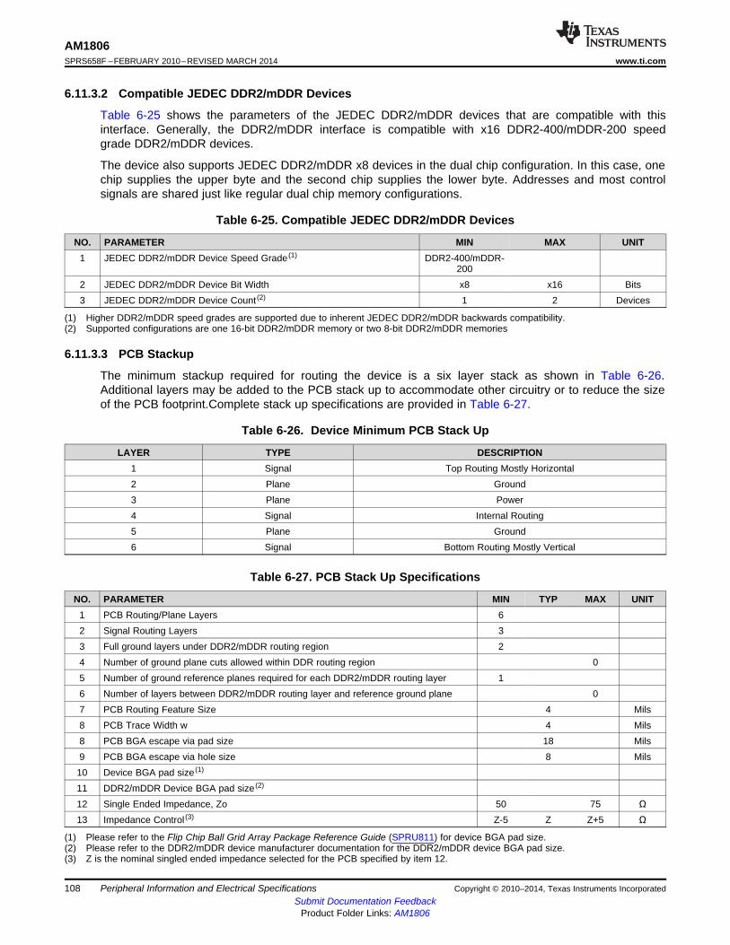
AM1806SPRS658F –FEBRUARY 2010–REVISED MARCH 2014 www.ti.com
6.11.3.2 Compatible JEDEC DDR2/mDDR Devices
Table 6-25 shows the parameters of the JEDEC DDR2/mDDR devices that are compatible with thisinterface. Generally, the DDR2/mDDR interface is compatible with x16 DDR2-400/mDDR-200 speedgrade DDR2/mDDR devices.
The device also supports JEDEC DDR2/mDDR x8 devices in the dual chip configuration. In this case, onechip supplies the upper byte and the second chip supplies the lower byte. Addresses and most controlsignals are shared just like regular dual chip memory configurations.
Table 6-25. Compatible JEDEC DDR2/mDDR Devices
NO. PARAMETER MIN MAX UNIT1 JEDEC DDR2/mDDR Device Speed Grade (1) DDR2-400/mDDR-
2002 JEDEC DDR2/mDDR Device Bit Width x8 x16 Bits3 JEDEC DDR2/mDDR Device Count (2) 1 2 Devices
(1) Higher DDR2/mDDR speed grades are supported due to inherent JEDEC DDR2/mDDR backwards compatibility.(2) Supported configurations are one 16-bit DDR2/mDDR memory or two 8-bit DDR2/mDDR memories
6.11.3.3 PCB Stackup
The minimum stackup required for routing the device is a six layer stack as shown in Table 6-26.Additional layers may be added to the PCB stack up to accommodate other circuitry or to reduce the sizeof the PCB footprint.Complete stack up specifications are provided in Table 6-27.
Table 6-26. Device Minimum PCB Stack Up
LAYER TYPE DESCRIPTION1 Signal Top Routing Mostly Horizontal2 Plane Ground3 Plane Power4 Signal Internal Routing5 Plane Ground6 Signal Bottom Routing Mostly Vertical
Table 6-27. PCB Stack Up Specifications
NO. PARAMETER MIN TYP MAX UNIT1 PCB Routing/Plane Layers 62 Signal Routing Layers 33 Full ground layers under DDR2/mDDR routing region 24 Number of ground plane cuts allowed within DDR routing region 05 Number of ground reference planes required for each DDR2/mDDR routing layer 16 Number of layers between DDR2/mDDR routing layer and reference ground plane 07 PCB Routing Feature Size 4 Mils8 PCB Trace Width w 4 Mils8 PCB BGA escape via pad size 18 Mils9 PCB BGA escape via hole size 8 Mils10 Device BGA pad size (1)
11 DDR2/mDDR Device BGA pad size (2)
12 Single Ended Impedance, Zo 50 75 Ω13 Impedance Control (3) Z-5 Z Z+5 Ω
(1) Please refer to the Flip Chip Ball Grid Array Package Reference Guide (SPRU811) for device BGA pad size.(2) Please refer to the DDR2/mDDR device manufacturer documentation for the DDR2/mDDR device BGA pad size.(3) Z is the nominal singled ended impedance selected for the PCB specified by item 12.
108 Peripheral Information and Electrical Specifications Copyright © 2010–2014, Texas Instruments IncorporatedSubmit Documentation Feedback
Product Folder Links: AM1806
A1
A1
X
Y
OFFSET
Recommended DDR2/mDDR
Device Orientation
Y
Y
OFFSET
DDR2/mDDR
Device
DD
R2/m
DD
R
Co
ntr
oller
AM1806www.ti.com SPRS658F –FEBRUARY 2010–REVISED MARCH 2014
6.11.3.4 Placement
Figure 6-17 shows the required placement for the device as well as the DDR2/mDDR devices. Thedimensions for Figure 6-18 are defined in Table 6-28. The placement does not restrict the side of the PCBthat the devices are mounted on. The ultimate purpose of the placement is to limit the maximum tracelengths and allow for proper routing space. For single-memory DDR2/mDDR systems, the secondDDR2/mDDR device is omitted from the placement.
Figure 6-18. Device and DDR2/mDDR Device Placement
Table 6-28. Placement Specifications (1) (2)
NO. PARAMETER MIN MAX UNIT1 X 1750 Mils2 Y 1280 Mils3 Y Offset (3)650 Mils4 Clearance from non-DDR2/mDDR signal to DDR2/mDDR Keepout Region (4) 4 w (5)
(1) See Figure 6-18 for dimension definitions.(2) Measurements from center of device to center of DDR2/mDDR device.(3) For single memory systems it is recommended that Y Offset be as small as possible.(4) Non-DDR2/mDDR signals allowed within DDR2/mDDR keepout region provided they are separated from DDR2/mDDR routing layers by
a ground plane.(5) w = PCB trace width as defined in Table 6-27.
Copyright © 2010–2014, Texas Instruments Incorporated Peripheral Information and Electrical Specifications 109Submit Documentation Feedback
Product Folder Links: AM1806
A1
A1
DD
R2/m
DD
RC
on
tro
ller
DDR2/mDDRDevice
Region should encompass all DDR2/mDDR circuitry and variesdepending on placement. Non-DDR2/mDDR signals should not berouted on the DDR signal layers within the DDR2/mDDR keep outregion. Non-DDR2/mDDR signals may be routed in the regionprovided they are routed on layers separated from DDR2/mDDRsignal layers by a ground layer. No breaks should be allowed in thereference ground layers in this region. In addition, the 1.8 V powerplane should cover the entire keep out region.
AM1806SPRS658F –FEBRUARY 2010–REVISED MARCH 2014 www.ti.com
6.11.3.5 DDR2/mDDR Keep Out Region
The region of the PCB used for the DDR2/mDDR circuitry must be isolated from other signals. TheDDR2/mDDR keep out region is defined for this purpose and is shown in Figure 6-19. The size of thisregion varies with the placement and DDR routing. Additional clearances required for the keep out regionare shown in Table 6-28.
Figure 6-19. DDR2/mDDR Keepout Region
110 Peripheral Information and Electrical Specifications Copyright © 2010–2014, Texas Instruments IncorporatedSubmit Documentation Feedback
Product Folder Links: AM1806
AM1806www.ti.com SPRS658F –FEBRUARY 2010–REVISED MARCH 2014
6.11.3.6 Bulk Bypass Capacitors
Bulk bypass capacitors are required for moderate speed bypassing of the DDR2/mDDR and othercircuitry. Table 6-29 contains the minimum numbers and capacitance required for the bulk bypasscapacitors. Note that this table only covers the bypass needs of the device and DDR2/mDDR interfaces.Additional bulk bypass capacitance may be needed for other circuitry.
Table 6-29. Bulk Bypass Capacitors
NO. PARAMETER MIN MAX UNIT1 DDR_DVDD18 Supply Bulk Bypass Capacitor Count (1) 3 Devices2 DDR_DVDD18 Supply Bulk Bypass Total Capacitance 30 μF3 DDR#1 Bulk Bypass Capacitor Count (1) 1 Devices4 DDR#1 Bulk Bypass Total Capacitance 22 μF5 DDR#2 Bulk Bypass Capacitor Count (1) (2) 1 Devices6 DDR#2 Bulk Bypass Total Capacitance (2) 22 μF
(1) These devices should be placed near the device they are bypassing, but preference should be given to the placement of the high-speed(HS) bypass caps.
(2) Only used on dual-memory systems.
6.11.3.7 High-Speed Bypass Capacitors
High-speed (HS) bypass capacitors are critical for proper DDR2/mDDR interface operation. It isparticularly important to minimize the parasitic series inductance of the HS bypass cap,device/DDR2/mDDR power, and device/DDR2/mDDR ground connections. Table 6-30 contains thespecification for the HS bypass capacitors as well as for the power connections on the PCB.
Table 6-30. High-Speed Bypass Capacitors
NO. PARAMETER MIN MAX UNIT1 HS Bypass Capacitor Package Size (1) 0402 10 Mils2 Distance from HS bypass capacitor to device being bypassed 250 Mils3 Number of connection vias for each HS bypass capacitor 2 (2) Vias4 Trace length from bypass capacitor contact to connection via 1 30 Mils5 Number of connection vias for each DDR2/mDDR device power or ground balls 1 Vias6 Trace length from DDR2/mDDR device power ball to connection via 35 Mils7 DDR_DVDD18 Supply HS Bypass Capacitor Count (3) 10 Devices8 DDR_DVDD18 Supply HS Bypass Capacitor Total Capacitance 0.6 μF9 DDR#1 HS Bypass Capacitor Count (3) 8 Devices10 DDR#1 HS Bypass Capacitor Total Capacitance 0.4 μF11 DDR#2 HS Bypass Capacitor Count (3) (4) 8 Devices12 DDR#2 HS Bypass Capacitor Total Capacitance (4) 0.4 μF
(1) LxW, 10 mil units, i.e., a 0402 is a 40x20 mil surface mount capacitor(2) An additional HS bypass capacitor can share the connection vias only if it is mounted on the opposite side of the board.(3) These devices should be placed as close as possible to the device being bypassed.(4) Only used on dual-memory systems.
Copyright © 2010–2014, Texas Instruments Incorporated Peripheral Information and Electrical Specifications 111Submit Documentation Feedback
Product Folder Links: AM1806
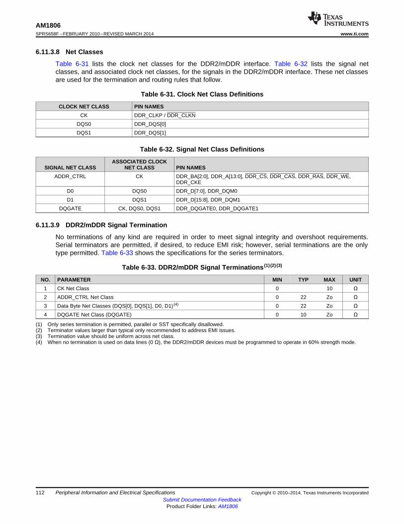
AM1806SPRS658F –FEBRUARY 2010–REVISED MARCH 2014 www.ti.com
6.11.3.8 Net Classes
Table 6-31 lists the clock net classes for the DDR2/mDDR interface. Table 6-32 lists the signal netclasses, and associated clock net classes, for the signals in the DDR2/mDDR interface. These net classesare used for the termination and routing rules that follow.
Table 6-31. Clock Net Class Definitions
CLOCK NET CLASS PIN NAMESCK DDR_CLKP / DDR_CLKN
DQS0 DDR_DQS[0]DQS1 DDR_DQS[1]
Table 6-32. Signal Net Class Definitions
ASSOCIATED CLOCKSIGNAL NET CLASS NET CLASS PIN NAMES
ADDR_CTRL CK DDR_BA[2:0], DDR_A[13:0], DDR_CS, DDR_CAS, DDR_RAS, DDR_WE,DDR_CKE
D0 DQS0 DDR_D[7:0], DDR_DQM0D1 DQS1 DDR_D[15:8], DDR_DQM1
DQGATE CK, DQS0, DQS1 DDR_DQGATE0, DDR_DQGATE1
6.11.3.9 DDR2/mDDR Signal Termination
No terminations of any kind are required in order to meet signal integrity and overshoot requirements.Serial terminators are permitted, if desired, to reduce EMI risk; however, serial terminations are the onlytype permitted. Table 6-33 shows the specifications for the series terminators.
Table 6-33. DDR2/mDDR Signal Terminations (1) (2) (3)
NO. PARAMETER MIN TYP MAX UNIT1 CK Net Class 0 10 Ω2 ADDR_CTRL Net Class 0 22 Zo Ω3 Data Byte Net Classes (DQS[0], DQS[1], D0, D1) (4) 0 22 Zo Ω4 DQGATE Net Class (DQGATE) 0 10 Zo Ω
(1) Only series termination is permitted, parallel or SST specifically disallowed.(2) Terminator values larger than typical only recommended to address EMI issues.(3) Termination value should be uniform across net class.(4) When no termination is used on data lines (0 Ω), the DDR2/mDDR devices must be programmed to operate in 60% strength mode.
112 Peripheral Information and Electrical Specifications Copyright © 2010–2014, Texas Instruments IncorporatedSubmit Documentation Feedback
Product Folder Links: AM1806
A1
A1
DDR2/mDDR Device
VREF Nominal Minimum
Trace Width is 20 Mils
VREF Bypass Capacitor
Neck down to minimum in BGA escape
regions is acceptable. Narrowing to
accomodate via congestion for short
distances is also acceptable. Best
performance is obtained if the width
of VREF is maximized.
DDR2/mDDR
AM1806www.ti.com SPRS658F –FEBRUARY 2010–REVISED MARCH 2014
6.11.3.10 VREF Routing
VREF is used as a reference by the input buffers of the DDR2/mDDR memories as well as the device.VREF is intended to be half the DDR2/mDDR power supply voltage and should be created using aresistive divider as shown in Figure 6-16. Other methods of creating VREF are not recommended.Figure 6-20 shows the layout guidelines for VREF.
Figure 6-20. VREF Routing and Topology
Copyright © 2010–2014, Texas Instruments Incorporated Peripheral Information and Electrical Specifications 113Submit Documentation Feedback
Product Folder Links: AM1806
A1
A1
CB
A
T
DD
R2/m
DD
R
Co
ntr
oller
AM1806SPRS658F –FEBRUARY 2010–REVISED MARCH 2014 www.ti.com
6.11.3.11 DDR2/mDDR CK and ADDR_CTRL Routing
Figure 6-21 shows the topology of the routing for the CK and ADDR_CTRL net classes. The route is abalanced T as it is intended that the length of segments B and C be equal. In addition, the length of Ashould be maximized.
Figure 6-21. CK and ADDR_CTRL Routing and Topology
Table 6-34. CK and ADDR_CTRL Routing Specification
NO. PARAMETER MIN TYP MAX UNIT1 Center to Center CK-CKN Spacing (1) 2w (2)
2 CK A to B/A to C Skew Length Mismatch (3) 25 Mils3 CK B to C Skew Length Mismatch 25 Mils4 Center to center CK to other DDR2/mDDR trace spacing (1) 4w (2)
5 CK/ADDR_CTRL nominal trace length (4) CACLM-50 CACLM CACLM+50 Mils6 ADDR_CTRL to CK Skew Length Mismatch 100 Mils7 ADDR_CTRL to ADDR_CTRL Skew Length Mismatch 100 Mils8 Center to center ADDR_CTRL to other DDR2/mDDR trace spacing (1) 4w (2)
9 Center to center ADDR_CTRL to other ADDR_CTRL trace spacing (1) 3w (2)
10 ADDR_CTRL A to B/A to C Skew Length Mismatch (3) 100 Mils11 ADDR_CTRL B to C Skew Length Mismatch 100 Mils
(1) Center to center spacing is allowed to fall to minimum (w) for up to 500 mils of routed length to accommodate BGA escape and routingcongestion.
(2) w = PCB trace width as defined in Table 6-27.(3) Series terminator, if used, should be located closest to device.(4) CACLM is the longest Manhattan distance of the CK and ADDR_CTRL net classes.
114 Peripheral Information and Electrical Specifications Copyright © 2010–2014, Texas Instruments IncorporatedSubmit Documentation Feedback
Product Folder Links: AM1806
A1
A1
E0
T
E1
DD
R2/m
DD
R
Co
ntr
oller
T
AM1806www.ti.com SPRS658F –FEBRUARY 2010–REVISED MARCH 2014
Figure 6-22 shows the topology and routing for the DQS and D net class; the routes are point to point.Skew matching across bytes is not needed nor recommended.
Figure 6-22. DQS and D Routing and Topology
Table 6-35. DQS and D Routing Specification
NO. PARAMETER MIN TYP MAX UNIT1 Center to center DQS to other DDR2/mDDR trace spacing (1) 4w (2)
2 DQS/D nominal trace length (3) (4) DQLM-50 DQLM DQLM+50 Mils3 D to DQS Skew Length Mismatch (4) 100 Mils4 D to D Skew Length Mismatch (4) 100 Mils5 Center to center D to other DDR2/mDDR trace spacing (1) (5) 4w (2)
6 Center to Center D to other D trace spacing (1) (6) 3w (2)
(1) Center to center spacing is allowed to fall to minimum (w) for up to 500 mils of routed length to accommodate BGA escape and routingcongestion.
(2) w = PCB trace width as defined in Table 6-27.(3) Series terminator, if used, should be located closest to DDR.(4) There is no need and it is not recommended to skew match across data bytes, i.e., from DQS0 and data byte 0 to DQS1 and data byte
1.(5) D's from other DQS domains are considered other DDR2/mDDR trace.(6) DQLM is the longest Manhattan distance of each of the DQS and D net class.
Copyright © 2010–2014, Texas Instruments Incorporated Peripheral Information and Electrical Specifications 115Submit Documentation Feedback
Product Folder Links: AM1806
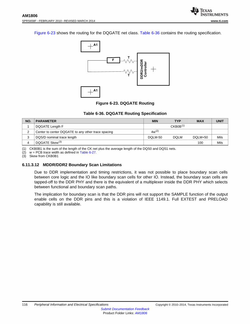
A1
A1
T
T
DD
R2/m
DD
R
Co
ntr
oller
F
AM1806SPRS658F –FEBRUARY 2010–REVISED MARCH 2014 www.ti.com
Figure 6-23 shows the routing for the DQGATE net class. Table 6-36 contains the routing specification.
Figure 6-23. DQGATE Routing
Table 6-36. DQGATE Routing Specification
NO. PARAMETER MIN TYP MAX UNIT1 DQGATE Length F CKB0B (1)
2 Center to center DQGATE to any other trace spacing 4w (2)
3 DQS/D nominal trace length DQLM-50 DQLM DQLM+50 Mils4 DQGATE Skew (3) 100 Mils
(1) CKB0B1 is the sum of the length of the CK net plus the average length of the DQS0 and DQS1 nets.(2) w = PCB trace width as defined in Table 6-27.(3) Skew from CKB0B1
6.11.3.12 MDDR/DDR2 Boundary Scan Limitations
Due to DDR implementation and timing restrictions, it was not possible to place boundary scan cellsbetween core logic and the IO like boundary scan cells for other IO. Instead, the boundary scan cells aretapped-off to the DDR PHY and there is the equivalent of a multiplexer inside the DDR PHY which selectsbetween functional and boundary scan paths.
The implication for boundary scan is that the DDR pins will not support the SAMPLE function of the outputenable cells on the DDR pins and this is a violation of IEEE 1149.1. Full EXTEST and PRELOADcapability is still available.
116 Peripheral Information and Electrical Specifications Copyright © 2010–2014, Texas Instruments IncorporatedSubmit Documentation Feedback
Product Folder Links: AM1806
AM1806www.ti.com SPRS658F –FEBRUARY 2010–REVISED MARCH 2014
6.12 Memory Protection UnitsThe MPU performs memory protection checking. It receives requests from a bus master in the system andchecks the address against the fixed and programmable regions to see if the access is allowed. If allowed,the transfer is passed unmodified to its output bus (to the targeted address). If the transfer is illegal (failsthe protection check) then the MPU does not pass the transfer to the output bus but rather services thetransfer internally back to the input bus (to prevent a hang) returning the fault status to the requestor aswell as generating an interrupt about the fault. The following features are supported by the MPU:• Provides memory protection for fixed and programmable address ranges.• Supports multiple programmable address region.• Supports secure and debug access privileges.• Supports read, write, and execute access privileges.• Supports privid(8) associations with ranges.• Generates an interrupt when there is a protection violation, and saves violating transfer parameters.• MMR access is also protected.
Table 6-37. MPU1 Configuration Registers
MPU1 ACRONYM REGISTER DESCRIPTIONBYTE ADDRESS0x01E1 4000 REVID Revision ID0x01E1 4004 CONFIG Configuration0x01E1 4010 IRAWSTAT Interrupt raw status/set0x01E1 4014 IENSTAT Interrupt enable status/clear0x01E1 4018 IENSET Interrupt enable0x01E1 401C IENCLR Interrupt enable clear
0x01E1 4020 - 0x01E1 41FF - Reserved0x01E1 4200 PROG1_MPSAR Programmable range 1, start address0x01E1 4204 PROG1_MPEAR Programmable range 1, end address0x01E1 4208 PROG1_MPPA Programmable range 1, memory page protection attributes
0x01E1 420C - 0x01E1 420F - Reserved0x01E1 4210 PROG2_MPSAR Programmable range 2, start address0x01E1 4214 PROG2_MPEAR Programmable range 2, end address0x01E1 4218 PROG2_MPPA Programmable range 2, memory page protection attributes
0x01E1 421C - 0x01E1 421F - Reserved0x01E1 4220 PROG3_MPSAR Programmable range 3, start address0x01E1 4224 PROG3_MPEAR Programmable range 3, end address0x01E1 4228 PROG3_MPPA Programmable range 3, memory page protection attributes
0x01E1 422C - 0x01E1 422F - Reserved0x01E1 4230 PROG4_MPSAR Programmable range 4, start address0x01E1 4234 PROG4_MPEAR Programmable range 4, end address0x01E1 4238 PROG4_MPPA Programmable range 4, memory page protection attributes
0x01E1 423C - 0x01E1 423F - Reserved0x01E1 4240 PROG5_MPSAR Programmable range 5, start address0x01E1 4244 PROG5_MPEAR Programmable range 5, end address0x01E1 4248 PROG5_MPPA Programmable range 5, memory page protection attributes
0x01E1 424C - 0x01E1 424F - Reserved0x01E1 4250 PROG6_MPSAR Programmable range 6, start address0x01E1 4254 PROG6_MPEAR Programmable range 6, end address0x01E1 4258 PROG6_MPPA Programmable range 6, memory page protection attributes
0x01E1 425C - 0x01E1 42FF - Reserved
Copyright © 2010–2014, Texas Instruments Incorporated Peripheral Information and Electrical Specifications 117Submit Documentation Feedback
Product Folder Links: AM1806
AM1806SPRS658F –FEBRUARY 2010–REVISED MARCH 2014 www.ti.com
Table 6-37. MPU1 Configuration Registers (continued)MPU1 ACRONYM REGISTER DESCRIPTIONBYTE ADDRESS
0x01E1 4300 FLTADDRR Fault address0x01E1 4304 FLTSTAT Fault status0x01E1 4308 FLTCLR Fault clear
0x01E1 430C - 0x01E1 4FFF - Reserved
Table 6-38. MPU2 Configuration Registers
MPU2 ACRONYM REGISTER DESCRIPTIONBYTE ADDRESS0x01E1 5000 REVID Revision ID0x01E1 5004 CONFIG Configuration0x01E1 5010 IRAWSTAT Interrupt raw status/set0x01E1 5014 IENSTAT Interrupt enable status/clear0x01E1 5018 IENSET Interrupt enable0x01E1 501C IENCLR Interrupt enable clear
0x01E1 5020 - 0x01E1 51FF - Reserved0x01E1 5200 PROG1_MPSAR Programmable range 1, start address0x01E1 5204 PROG1_MPEAR Programmable range 1, end address0x01E1 5208 PROG1_MPPA Programmable range 1, memory page protection attributes
0x01E1 520C - 0x01E1 520F - Reserved0x01E1 5210 PROG2_MPSAR Programmable range 2, start address0x01E1 5214 PROG2_MPEAR Programmable range 2, end address0x01E1 5218 PROG2_MPPA Programmable range 2, memory page protection attributes
0x01E1 521C - 0x01E1 521F - Reserved0x01E1 5220 PROG3_MPSAR Programmable range 3, start address0x01E1 5224 PROG3_MPEAR Programmable range 3, end address0x01E1 5228 PROG3_MPPA Programmable range 3, memory page protection attributes
0x01E1 522C - 0x01E1 522F - Reserved0x01E1 5230 PROG4_MPSAR Programmable range 4, start address0x01E1 5234 PROG4_MPEAR Programmable range 4, end address0x01E1 5238 PROG4_MPPA Programmable range 4, memory page protection attributes
0x01E1 523C - 0x01E1 523F - Reserved0x01E1 5240 PROG5_MPSAR Programmable range 5, start address0x01E1 5244 PROG5_MPEAR Programmable range 5, end address0x01E1 5248 PROG5_MPPA Programmable range 5, memory page protection attributes
0x01E1 524C - 0x01E1 524F - Reserved0x01E1 5250 PROG6_MPSAR Programmable range 6, start address0x01E1 5254 PROG6_MPEAR Programmable range 6, end address0x01E1 5258 PROG6_MPPA Programmable range 6, memory page protection attributes
0x01E1 525C - 0x01E1 525F - Reserved0x01E1 5260 PROG7_MPSAR Programmable range 7, start address0x01E1 5264 PROG7_MPEAR Programmable range 7, end address0x01E1 5268 PROG7_MPPA Programmable range 7, memory page protection attributes
0x01E1 526C - 0x01E1 526F - Reserved0x01E1 5270 PROG8_MPSAR Programmable range 8, start address0x01E1 5274 PROG8_MPEAR Programmable range 8, end address0x01E1 5278 PROG8_MPPA Programmable range 8, memory page protection attributes
0x01E1 527C - 0x01E1 527F - Reserved
118 Peripheral Information and Electrical Specifications Copyright © 2010–2014, Texas Instruments IncorporatedSubmit Documentation Feedback
Product Folder Links: AM1806
AM1806www.ti.com SPRS658F –FEBRUARY 2010–REVISED MARCH 2014
Table 6-38. MPU2 Configuration Registers (continued)MPU2 ACRONYM REGISTER DESCRIPTIONBYTE ADDRESS
0x01E1 5280 PROG9_MPSAR Programmable range 9, start address0x01E1 5284 PROG9_MPEAR Programmable range 9, end address0x01E1 5288 PROG9_MPPA Programmable range 9, memory page protection attributes
0x01E1 528C - 0x01E1 528F - Reserved0x01E1 5290 PROG10_MPSAR Programmable range 10, start address0x01E1 5294 PROG10_MPEAR Programmable range 10, end address0x01E1 5298 PROG10_MPPA Programmable range 10, memory page protection attributes
0x01E1 529C - 0x01E1 529F - Reserved0x01E1 52A0 PROG11_MPSAR Programmable range 11, start address0x01E1 52A4 PROG11_MPEAR Programmable range 11, end address0x01E1 52A8 PROG11_MPPA Programmable range 11, memory page protection attributes
0x01E1 52AC - 0x01E1 52AF - Reserved0x01E1 52B0 PROG12_MPSAR Programmable range 12, start address0x01E1 52B4 PROG12_MPEAR Programmable range 12, end address0x01E1 52B8 PROG12_MPPA Programmable range 12, memory page protection attributes
0x01E1 52BC - 0x01E1 52FF - Reserved0x01E1 5300 FLTADDRR Fault address0x01E1 5304 FLTSTAT Fault status0x01E1 5308 FLTCLR Fault clear
0x01E1 530C - 0x01E1 5FFF - Reserved
Copyright © 2010–2014, Texas Instruments Incorporated Peripheral Information and Electrical Specifications 119Submit Documentation Feedback
Product Folder Links: AM1806
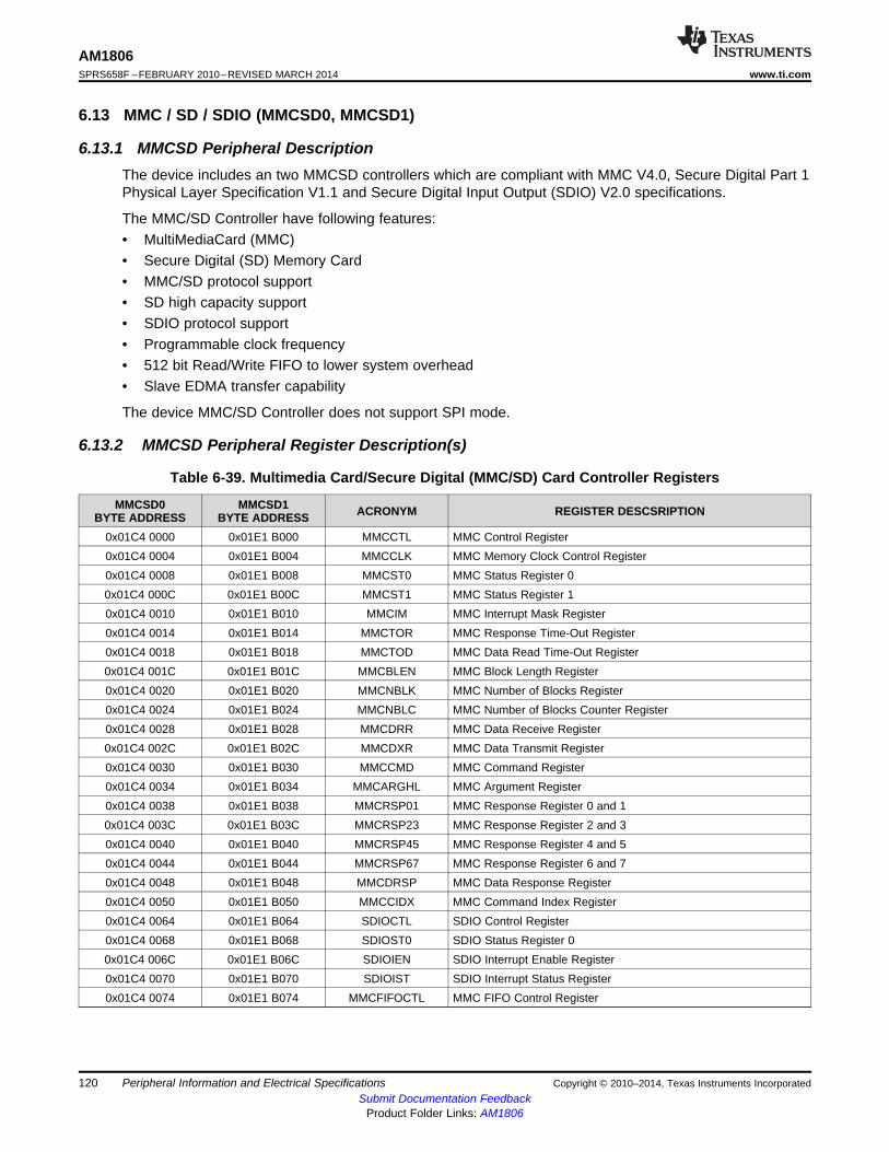
AM1806SPRS658F –FEBRUARY 2010–REVISED MARCH 2014 www.ti.com
6.13 MMC / SD / SDIO (MMCSD0, MMCSD1)
6.13.1 MMCSD Peripheral DescriptionThe device includes an two MMCSD controllers which are compliant with MMC V4.0, Secure Digital Part 1Physical Layer Specification V1.1 and Secure Digital Input Output (SDIO) V2.0 specifications.
The MMC/SD Controller have following features:• MultiMediaCard (MMC)• Secure Digital (SD) Memory Card• MMC/SD protocol support• SD high capacity support• SDIO protocol support• Programmable clock frequency• 512 bit Read/Write FIFO to lower system overhead• Slave EDMA transfer capability
The device MMC/SD Controller does not support SPI mode.
6.13.2 MMCSD Peripheral Register Description(s)
Table 6-39. Multimedia Card/Secure Digital (MMC/SD) Card Controller Registers
MMCSD0 MMCSD1 ACRONYM REGISTER DESCSRIPTIONBYTE ADDRESS BYTE ADDRESS0x01C4 0000 0x01E1 B000 MMCCTL MMC Control Register0x01C4 0004 0x01E1 B004 MMCCLK MMC Memory Clock Control Register0x01C4 0008 0x01E1 B008 MMCST0 MMC Status Register 00x01C4 000C 0x01E1 B00C MMCST1 MMC Status Register 10x01C4 0010 0x01E1 B010 MMCIM MMC Interrupt Mask Register0x01C4 0014 0x01E1 B014 MMCTOR MMC Response Time-Out Register0x01C4 0018 0x01E1 B018 MMCTOD MMC Data Read Time-Out Register0x01C4 001C 0x01E1 B01C MMCBLEN MMC Block Length Register0x01C4 0020 0x01E1 B020 MMCNBLK MMC Number of Blocks Register0x01C4 0024 0x01E1 B024 MMCNBLC MMC Number of Blocks Counter Register0x01C4 0028 0x01E1 B028 MMCDRR MMC Data Receive Register0x01C4 002C 0x01E1 B02C MMCDXR MMC Data Transmit Register0x01C4 0030 0x01E1 B030 MMCCMD MMC Command Register0x01C4 0034 0x01E1 B034 MMCARGHL MMC Argument Register0x01C4 0038 0x01E1 B038 MMCRSP01 MMC Response Register 0 and 10x01C4 003C 0x01E1 B03C MMCRSP23 MMC Response Register 2 and 30x01C4 0040 0x01E1 B040 MMCRSP45 MMC Response Register 4 and 50x01C4 0044 0x01E1 B044 MMCRSP67 MMC Response Register 6 and 70x01C4 0048 0x01E1 B048 MMCDRSP MMC Data Response Register0x01C4 0050 0x01E1 B050 MMCCIDX MMC Command Index Register0x01C4 0064 0x01E1 B064 SDIOCTL SDIO Control Register0x01C4 0068 0x01E1 B068 SDIOST0 SDIO Status Register 00x01C4 006C 0x01E1 B06C SDIOIEN SDIO Interrupt Enable Register0x01C4 0070 0x01E1 B070 SDIOIST SDIO Interrupt Status Register0x01C4 0074 0x01E1 B074 MMCFIFOCTL MMC FIFO Control Register
120 Peripheral Information and Electrical Specifications Copyright © 2010–2014, Texas Instruments IncorporatedSubmit Documentation Feedback
Product Folder Links: AM1806
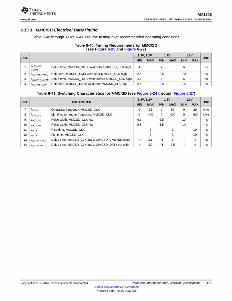
AM1806www.ti.com SPRS658F –FEBRUARY 2010–REVISED MARCH 2014
6.13.3 MMC/SD Electrical Data/TimingTable 6-40 through Table 6-41 assume testing over recommended operating conditions.
Table 6-40. Timing Requirements for MMC/SD(see Figure 6-25 and Figure 6-27)
1.3V, 1.2V 1.1V 1.0VNO. UNIT
MIN MAX MIN MAX MIN MAXtsu(CMDV-1 Setup time, MMCSD_CMD valid before MMCSD_CLK high 4 4 6 nsCLKH)
2 th(CLKH-CMDV) Hold time, MMCSD_CMD valid after MMCSD_CLK high 2.5 2.5 2.5 ns3 tsu(DATV-CLKH) Setup time, MMCSD_DATx valid before MMCSD_CLK high 4.5 5 6 ns4 th(CLKH-DATV) Hold time, MMCSD_DATx valid after MMCSD_CLK high 2.5 2.5 2.5 ns
Table 6-41. Switching Characteristics for MMC/SD (see Figure 6-24 through Figure 6-27)1.3V, 1.2V 1.1V 1.0V
NO. PARAMETER UNITMIN MAX MIN MAX MIN MAX
7 f(CLK) Operating frequency, MMCSD_CLK 0 52 0 50 0 25 MHz8 f(CLK_ID) Identification mode frequency, MMCSD_CLK 0 400 0 400 0 400 KHz9 tW(CLKL) Pulse width, MMCSD_CLK low 6.5 6.5 10 ns
10 tW(CLKH) Pulse width, MMCSD_CLK high 6.5 6.5 10 ns11 tr(CLK) Rise time, MMCSD_CLK 3 3 10 ns12 tf(CLK) Fall time, MMCSD_CLK 3 3 10 ns13 td(CLKL-CMD) Delay time, MMCSD_CLK low to MMCSD_CMD transition -4 2.5 -4 3 -4 4 ns14 td(CLKL-DAT) Delay time, MMCSD_CLK low to MMCSD_DATx transition -4 3.3 -4 3.5 -4 4 ns
Copyright © 2010–2014, Texas Instruments Incorporated Peripheral Information and Electrical Specifications 121Submit Documentation Feedback
Product Folder Links: AM1806
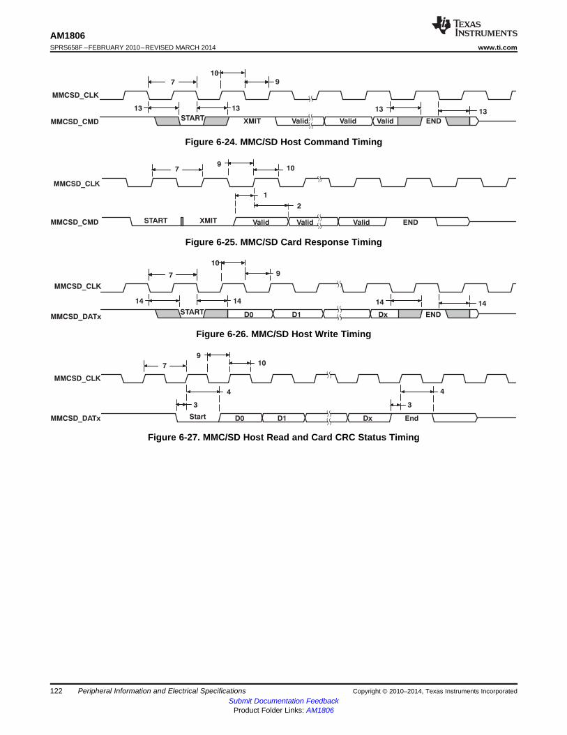
Start D0 D1 Dx End
7
MMCSD_CLK
MMCSD_DATx
910
4
3 3
4
START D0 D1 Dx END
MMCSD_CLK
MMCSD_DATx
7
1414
10
9
14 14
START XMIT Valid Valid Valid END
MMCSD_CLK
MMCSD_CMD
109
7
1
2
START XMIT Valid Valid Valid END
MMCSD_CLK
MMCSD_CMD
13
7
109
13 13 13
AM1806SPRS658F –FEBRUARY 2010–REVISED MARCH 2014 www.ti.com
Figure 6-24. MMC/SD Host Command Timing
Figure 6-25. MMC/SD Card Response Timing
Figure 6-26. MMC/SD Host Write Timing
Figure 6-27. MMC/SD Host Read and Card CRC Status Timing
122 Peripheral Information and Electrical Specifications Copyright © 2010–2014, Texas Instruments IncorporatedSubmit Documentation Feedback
Product Folder Links: AM1806
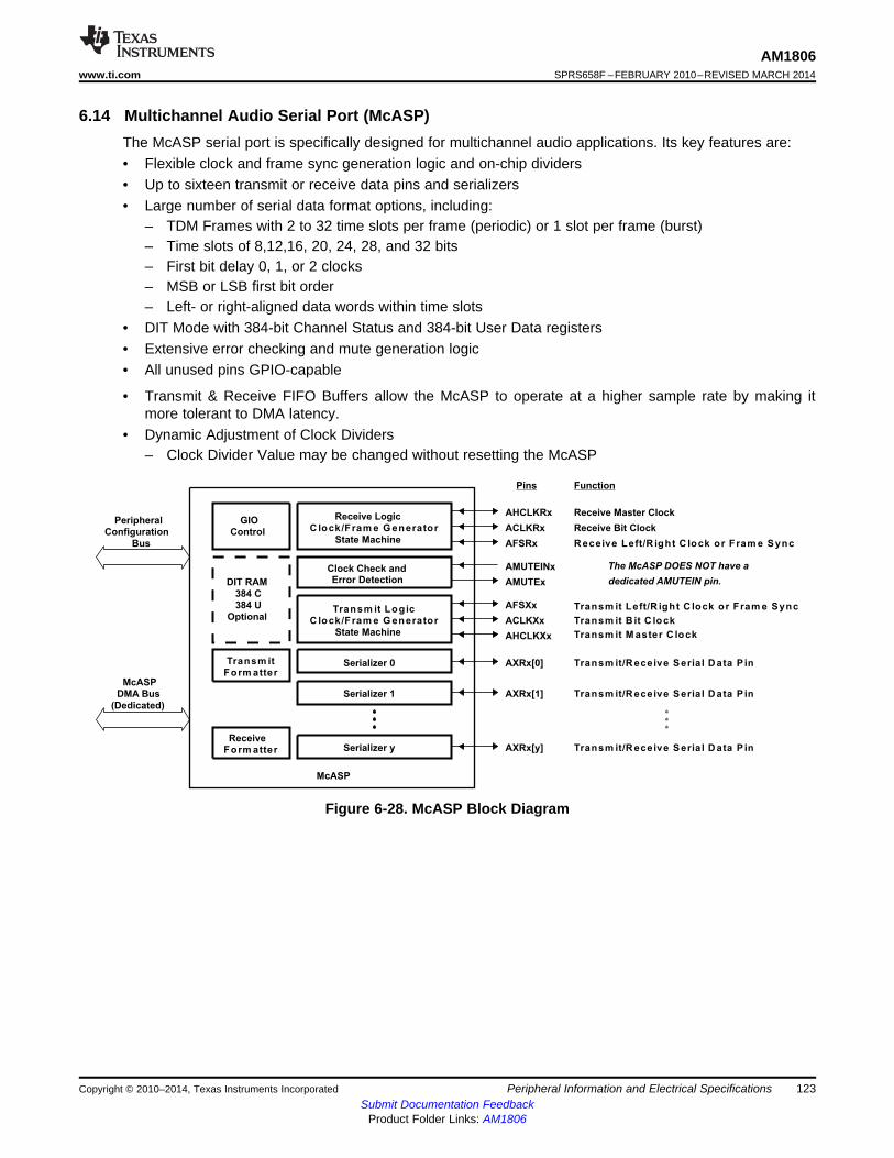
Receive Logic
C lock/Fram e G enerator
State Machine
Clock Check and
Serializer 0
Serializer 1
Serializer y
GIO
Control
DIT RAM
384 C
384 U
Optional
Transm it
Form atter
Receive
Form atter
Transm it Logic
C lock/Fram e G enerator
State Machine
McASP
Peripheral
Configuration
Bus
McASP
DMA Bus
(Dedicated)
AHCLKRx
ACLKRx
AFSRx
AMUTEINx
AMUTEx
AFSXx
ACLKXx
AHCLKXx
AXRx[0]
AXRx[1]
AXRx[y]
Pins Function
Receive Master Clock
Receive Bit Clock
R eceive Left/R ight C lock or Fram e Sync
Transm it M aster C lock
Transm it B it C lock
Transm it Left/R ight C lock or Fram e Sync
Transm it/R eceive Serial D ata P in
Transm it/R eceive Serial D ata P in
Transm it/R eceive Serial D ata P in
Error Detection
The McASP DOES NOT have a
dedicated AMUTEIN pin.
AM1806www.ti.com SPRS658F –FEBRUARY 2010–REVISED MARCH 2014
6.14 Multichannel Audio Serial Port (McASP)The McASP serial port is specifically designed for multichannel audio applications. Its key features are:• Flexible clock and frame sync generation logic and on-chip dividers• Up to sixteen transmit or receive data pins and serializers• Large number of serial data format options, including:
– TDM Frames with 2 to 32 time slots per frame (periodic) or 1 slot per frame (burst)– Time slots of 8,12,16, 20, 24, 28, and 32 bits– First bit delay 0, 1, or 2 clocks– MSB or LSB first bit order– Left- or right-aligned data words within time slots
• DIT Mode with 384-bit Channel Status and 384-bit User Data registers• Extensive error checking and mute generation logic• All unused pins GPIO-capable
• Transmit & Receive FIFO Buffers allow the McASP to operate at a higher sample rate by making itmore tolerant to DMA latency.
• Dynamic Adjustment of Clock Dividers– Clock Divider Value may be changed without resetting the McASP
Figure 6-28. McASP Block Diagram
Copyright © 2010–2014, Texas Instruments Incorporated Peripheral Information and Electrical Specifications 123Submit Documentation Feedback
Product Folder Links: AM1806
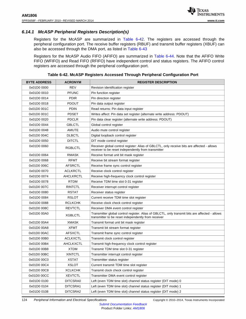
AM1806SPRS658F –FEBRUARY 2010–REVISED MARCH 2014 www.ti.com
6.14.1 McASP Peripheral Registers Description(s)Registers for the McASP are summarized in Table 6-42. The registers are accessed through theperipheral configuration port. The receive buffer registers (RBUF) and transmit buffer registers (XBUF) canalso be accessed through the DMA port, as listed in Table 6-43
Registers for the McASP Audio FIFO (AFIFO) are summarized in Table 6-44. Note that the AFIFO WriteFIFO (WFIFO) and Read FIFO (RFIFO) have independent control and status registers. The AFIFO controlregisters are accessed through the peripheral configuration port.
Table 6-42. McASP Registers Accessed Through Peripheral Configuration Port
BYTE ADDRESS ACRONYM REGISTER DESCRIPTION0x01D0 0000 REV Revision identification register0x01D0 0010 PFUNC Pin function register0x01D0 0014 PDIR Pin direction register0x01D0 0018 PDOUT Pin data output register0x01D0 001C PDIN Read returns: Pin data input register0x01D0 001C PDSET Writes affect: Pin data set register (alternate write address: PDOUT)0x01D0 0020 PDCLR Pin data clear register (alternate write address: PDOUT)0x01D0 0044 GBLCTL Global control register0x01D0 0048 AMUTE Audio mute control register0x01D0 004C DLBCTL Digital loopback control register0x01D0 0050 DITCTL DIT mode control register0x01D0 0060 Receiver global control register: Alias of GBLCTL, only receive bits are affected - allowsRGBLCTL receiver to be reset independently from transmitter0x01D0 0064 RMASK Receive format unit bit mask register0x01D0 0068 RFMT Receive bit stream format register0x01D0 006C AFSRCTL Receive frame sync control register0x01D0 0070 ACLKRCTL Receive clock control register0x01D0 0074 AHCLKRCTL Receive high-frequency clock control register0x01D0 0078 RTDM Receive TDM time slot 0-31 register0x01D0 007C RINTCTL Receiver interrupt control register0x01D0 0080 RSTAT Receiver status register0x01D0 0084 RSLOT Current receive TDM time slot register0x01D0 0088 RCLKCHK Receive clock check control register0x01D0 008C REVTCTL Receiver DMA event control register0x01D0 00A0 Transmitter global control register. Alias of GBLCTL, only transmit bits are affected - allowsXGBLCTL transmitter to be reset independently from receiver0x01D0 00A4 XMASK Transmit format unit bit mask register0x01D0 00A8 XFMT Transmit bit stream format register0x01D0 00AC AFSXCTL Transmit frame sync control register0x01D0 00B0 ACLKXCTL Transmit clock control register0x01D0 00B4 AHCLKXCTL Transmit high-frequency clock control register0x01D0 00B8 XTDM Transmit TDM time slot 0-31 register0x01D0 00BC XINTCTL Transmitter interrupt control register0x01D0 00C0 XSTAT Transmitter status register0x01D0 00C4 XSLOT Current transmit TDM time slot register0x01D0 00C8 XCLKCHK Transmit clock check control register0x01D0 00CC XEVTCTL Transmitter DMA event control register0x01D0 0100 DITCSRA0 Left (even TDM time slot) channel status register (DIT mode) 00x01D0 0104 DITCSRA1 Left (even TDM time slot) channel status register (DIT mode) 10x01D0 0108 DITCSRA2 Left (even TDM time slot) channel status register (DIT mode) 2
124 Peripheral Information and Electrical Specifications Copyright © 2010–2014, Texas Instruments IncorporatedSubmit Documentation Feedback
Product Folder Links: AM1806
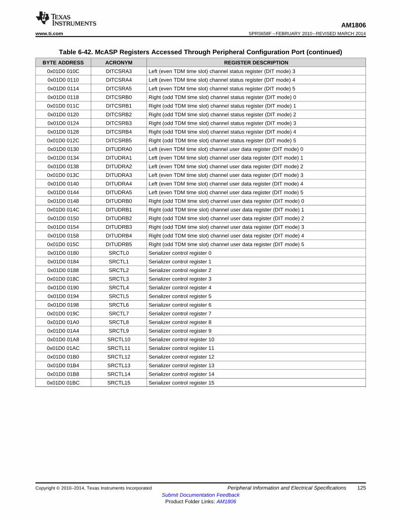
AM1806www.ti.com SPRS658F –FEBRUARY 2010–REVISED MARCH 2014
Table 6-42. McASP Registers Accessed Through Peripheral Configuration Port (continued)BYTE ADDRESS ACRONYM REGISTER DESCRIPTION
0x01D0 010C DITCSRA3 Left (even TDM time slot) channel status register (DIT mode) 30x01D0 0110 DITCSRA4 Left (even TDM time slot) channel status register (DIT mode) 40x01D0 0114 DITCSRA5 Left (even TDM time slot) channel status register (DIT mode) 50x01D0 0118 DITCSRB0 Right (odd TDM time slot) channel status register (DIT mode) 00x01D0 011C DITCSRB1 Right (odd TDM time slot) channel status register (DIT mode) 10x01D0 0120 DITCSRB2 Right (odd TDM time slot) channel status register (DIT mode) 20x01D0 0124 DITCSRB3 Right (odd TDM time slot) channel status register (DIT mode) 30x01D0 0128 DITCSRB4 Right (odd TDM time slot) channel status register (DIT mode) 40x01D0 012C DITCSRB5 Right (odd TDM time slot) channel status register (DIT mode) 50x01D0 0130 DITUDRA0 Left (even TDM time slot) channel user data register (DIT mode) 00x01D0 0134 DITUDRA1 Left (even TDM time slot) channel user data register (DIT mode) 10x01D0 0138 DITUDRA2 Left (even TDM time slot) channel user data register (DIT mode) 20x01D0 013C DITUDRA3 Left (even TDM time slot) channel user data register (DIT mode) 30x01D0 0140 DITUDRA4 Left (even TDM time slot) channel user data register (DIT mode) 40x01D0 0144 DITUDRA5 Left (even TDM time slot) channel user data register (DIT mode) 50x01D0 0148 DITUDRB0 Right (odd TDM time slot) channel user data register (DIT mode) 00x01D0 014C DITUDRB1 Right (odd TDM time slot) channel user data register (DIT mode) 10x01D0 0150 DITUDRB2 Right (odd TDM time slot) channel user data register (DIT mode) 20x01D0 0154 DITUDRB3 Right (odd TDM time slot) channel user data register (DIT mode) 30x01D0 0158 DITUDRB4 Right (odd TDM time slot) channel user data register (DIT mode) 40x01D0 015C DITUDRB5 Right (odd TDM time slot) channel user data register (DIT mode) 50x01D0 0180 SRCTL0 Serializer control register 00x01D0 0184 SRCTL1 Serializer control register 10x01D0 0188 SRCTL2 Serializer control register 20x01D0 018C SRCTL3 Serializer control register 30x01D0 0190 SRCTL4 Serializer control register 40x01D0 0194 SRCTL5 Serializer control register 50x01D0 0198 SRCTL6 Serializer control register 60x01D0 019C SRCTL7 Serializer control register 70x01D0 01A0 SRCTL8 Serializer control register 80x01D0 01A4 SRCTL9 Serializer control register 90x01D0 01A8 SRCTL10 Serializer control register 100x01D0 01AC SRCTL11 Serializer control register 110x01D0 01B0 SRCTL12 Serializer control register 120x01D0 01B4 SRCTL13 Serializer control register 130x01D0 01B8 SRCTL14 Serializer control register 140x01D0 01BC SRCTL15 Serializer control register 15
Copyright © 2010–2014, Texas Instruments Incorporated Peripheral Information and Electrical Specifications 125Submit Documentation Feedback
Product Folder Links: AM1806
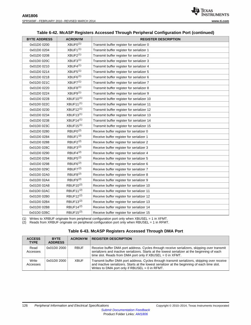
AM1806SPRS658F –FEBRUARY 2010–REVISED MARCH 2014 www.ti.com
Table 6-42. McASP Registers Accessed Through Peripheral Configuration Port (continued)BYTE ADDRESS ACRONYM REGISTER DESCRIPTION
0x01D0 0200 XBUF0 (1) Transmit buffer register for serializer 00x01D0 0204 XBUF1 (1) Transmit buffer register for serializer 10x01D0 0208 XBUF2 (1) Transmit buffer register for serializer 20x01D0 020C XBUF3 (1) Transmit buffer register for serializer 30x01D0 0210 XBUF4 (1) Transmit buffer register for serializer 40x01D0 0214 XBUF5 (1) Transmit buffer register for serializer 50x01D0 0218 XBUF6 (1) Transmit buffer register for serializer 60x01D0 021C XBUF7 (1) Transmit buffer register for serializer 70x01D0 0220 XBUF8 (1) Transmit buffer register for serializer 80x01D0 0224 XBUF9 (1) Transmit buffer register for serializer 90x01D0 0228 XBUF10 (1) Transmit buffer register for serializer 100x01D0 022C XBUF11 (1) Transmit buffer register for serializer 110x01D0 0230 XBUF12 (1) Transmit buffer register for serializer 120x01D0 0234 XBUF13 (1) Transmit buffer register for serializer 130x01D0 0238 XBUF14 (1) Transmit buffer register for serializer 140x01D0 023C XBUF15 (1) Transmit buffer register for serializer 150x01D0 0280 RBUF0 (2) Receive buffer register for serializer 00x01D0 0284 RBUF1 (2) Receive buffer register for serializer 10x01D0 0288 RBUF2 (2) Receive buffer register for serializer 20x01D0 028C RBUF3 (2) Receive buffer register for serializer 30x01D0 0290 RBUF4 (2) Receive buffer register for serializer 40x01D0 0294 RBUF5 (2) Receive buffer register for serializer 50x01D0 0298 RBUF6 (2) Receive buffer register for serializer 60x01D0 029C RBUF7 (2) Receive buffer register for serializer 70x01D0 02A0 RBUF8 (2) Receive buffer register for serializer 80x01D0 02A4 RBUF9 (2) Receive buffer register for serializer 90x01D0 02A8 RBUF10 (2) Receive buffer register for serializer 100x01D0 02AC RBUF11 (2) Receive buffer register for serializer 110x01D0 02B0 RBUF12 (2) Receive buffer register for serializer 120x01D0 02B4 RBUF13 (2) Receive buffer register for serializer 130x01D0 02B8 RBUF14 (2) Receive buffer register for serializer 140x01D0 02BC RBUF15 (2) Receive buffer register for serializer 15
(1) Writes to XRBUF originate from peripheral configuration port only when XBUSEL = 1 in XFMT.(2) Reads from XRBUF originate on peripheral configuration port only when RBUSEL = 1 in RFMT.
Table 6-43. McASP Registers Accessed Through DMA Port
ACCESS BYTE ACRONYM REGISTER DESCRIPTIONTYPE ADDRESSRead 0x01D0 2000 RBUF Receive buffer DMA port address. Cycles through receive serializers, skipping over transmit
Accesses serializers and inactive serializers. Starts at the lowest serializer at the beginning of eachtime slot. Reads from DMA port only if XBUSEL = 0 in XFMT.
Write 0x01D0 2000 XBUF Transmit buffer DMA port address. Cycles through transmit serializers, skipping over receiveAccesses and inactive serializers. Starts at the lowest serializer at the beginning of each time slot.
Writes to DMA port only if RBUSEL = 0 in RFMT.
126 Peripheral Information and Electrical Specifications Copyright © 2010–2014, Texas Instruments IncorporatedSubmit Documentation Feedback
Product Folder Links: AM1806
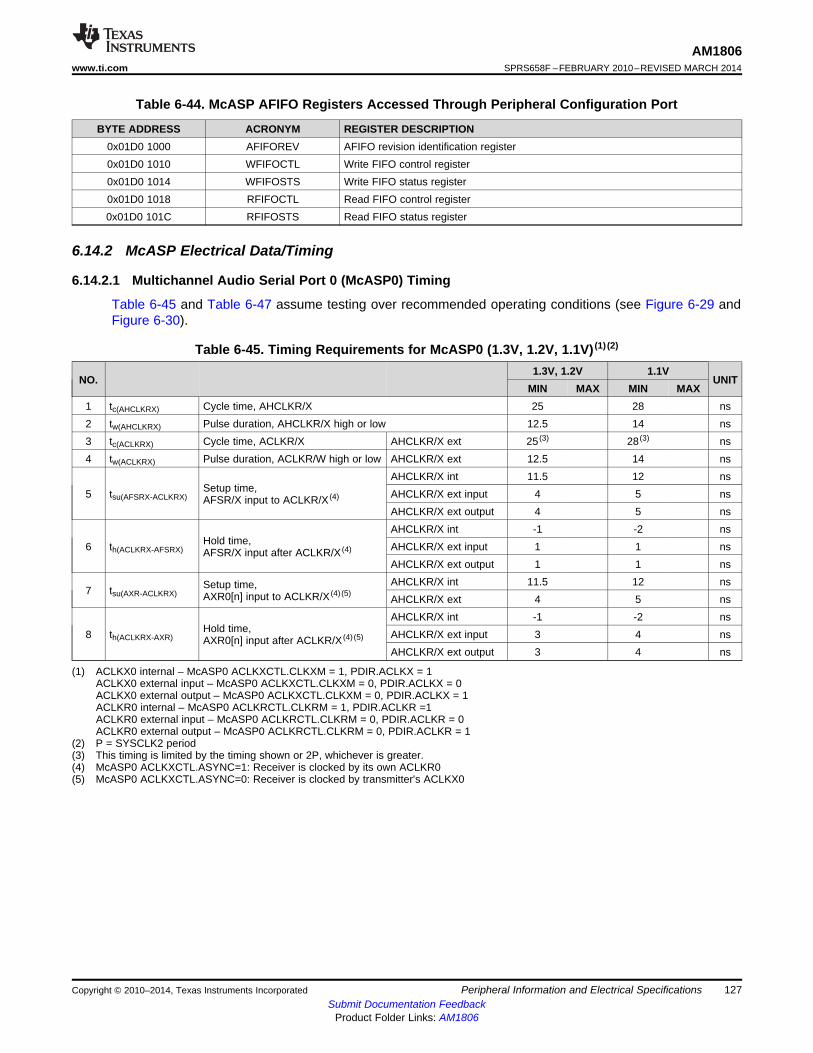
AM1806www.ti.com SPRS658F –FEBRUARY 2010–REVISED MARCH 2014
Table 6-44. McASP AFIFO Registers Accessed Through Peripheral Configuration Port
BYTE ADDRESS ACRONYM REGISTER DESCRIPTION0x01D0 1000 AFIFOREV AFIFO revision identification register0x01D0 1010 WFIFOCTL Write FIFO control register0x01D0 1014 WFIFOSTS Write FIFO status register0x01D0 1018 RFIFOCTL Read FIFO control register0x01D0 101C RFIFOSTS Read FIFO status register
6.14.2 McASP Electrical Data/Timing
6.14.2.1 Multichannel Audio Serial Port 0 (McASP0) Timing
Table 6-45 and Table 6-47 assume testing over recommended operating conditions (see Figure 6-29 andFigure 6-30).
Table 6-45. Timing Requirements for McASP0 (1.3V, 1.2V, 1.1V) (1) (2)
1.3V, 1.2V 1.1VNO. UNIT
MIN MAX MIN MAX1 tc(AHCLKRX) Cycle time, AHCLKR/X 25 28 ns2 tw(AHCLKRX) Pulse duration, AHCLKR/X high or low 12.5 14 ns3 tc(ACLKRX) Cycle time, ACLKR/X AHCLKR/X ext 25 (3) 28 (3) ns4 tw(ACLKRX) Pulse duration, ACLKR/W high or low AHCLKR/X ext 12.5 14 ns
AHCLKR/X int 11.5 12 nsSetup time,5 tsu(AFSRX-ACLKRX) AHCLKR/X ext input 4 5 nsAFSR/X input to ACLKR/X (4)
AHCLKR/X ext output 4 5 nsAHCLKR/X int -1 -2 ns
Hold time,6 th(ACLKRX-AFSRX) AHCLKR/X ext input 1 1 nsAFSR/X input after ACLKR/X (4)
AHCLKR/X ext output 1 1 nsAHCLKR/X int 11.5 12 nsSetup time,7 tsu(AXR-ACLKRX) AXR0[n] input to ACLKR/X (4) (5) AHCLKR/X ext 4 5 nsAHCLKR/X int -1 -2 ns
Hold time,8 th(ACLKRX-AXR) AHCLKR/X ext input 3 4 nsAXR0[n] input after ACLKR/X (4) (5)
AHCLKR/X ext output 3 4 ns
(1) ACLKX0 internal – McASP0 ACLKXCTL.CLKXM = 1, PDIR.ACLKX = 1ACLKX0 external input – McASP0 ACLKXCTL.CLKXM = 0, PDIR.ACLKX = 0ACLKX0 external output – McASP0 ACLKXCTL.CLKXM = 0, PDIR.ACLKX = 1ACLKR0 internal – McASP0 ACLKRCTL.CLKRM = 1, PDIR.ACLKR =1ACLKR0 external input – McASP0 ACLKRCTL.CLKRM = 0, PDIR.ACLKR = 0ACLKR0 external output – McASP0 ACLKRCTL.CLKRM = 0, PDIR.ACLKR = 1
(2) P = SYSCLK2 period(3) This timing is limited by the timing shown or 2P, whichever is greater.(4) McASP0 ACLKXCTL.ASYNC=1: Receiver is clocked by its own ACLKR0(5) McASP0 ACLKXCTL.ASYNC=0: Receiver is clocked by transmitter's ACLKX0
Copyright © 2010–2014, Texas Instruments Incorporated Peripheral Information and Electrical Specifications 127Submit Documentation Feedback
Product Folder Links: AM1806
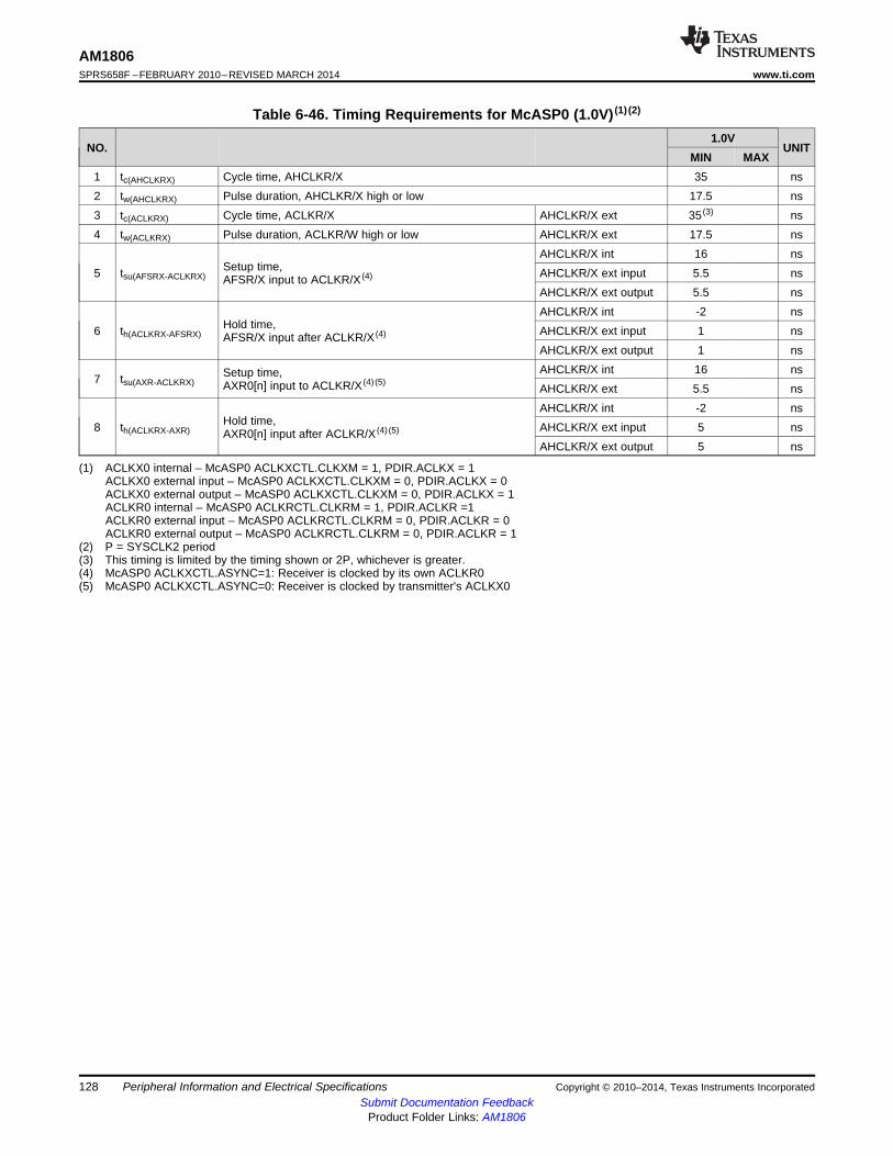
AM1806SPRS658F –FEBRUARY 2010–REVISED MARCH 2014 www.ti.com
Table 6-46. Timing Requirements for McASP0 (1.0V) (1) (2)
1.0VNO. UNIT
MIN MAX1 tc(AHCLKRX) Cycle time, AHCLKR/X 35 ns2 tw(AHCLKRX) Pulse duration, AHCLKR/X high or low 17.5 ns3 tc(ACLKRX) Cycle time, ACLKR/X AHCLKR/X ext 35 (3) ns4 tw(ACLKRX) Pulse duration, ACLKR/W high or low AHCLKR/X ext 17.5 ns
AHCLKR/X int 16 nsSetup time,5 tsu(AFSRX-ACLKRX) AHCLKR/X ext input 5.5 nsAFSR/X input to ACLKR/X (4)
AHCLKR/X ext output 5.5 nsAHCLKR/X int -2 ns
Hold time,6 th(ACLKRX-AFSRX) AHCLKR/X ext input 1 nsAFSR/X input after ACLKR/X (4)
AHCLKR/X ext output 1 nsAHCLKR/X int 16 nsSetup time,7 tsu(AXR-ACLKRX) AXR0[n] input to ACLKR/X (4) (5) AHCLKR/X ext 5.5 nsAHCLKR/X int -2 ns
Hold time,8 th(ACLKRX-AXR) AHCLKR/X ext input 5 nsAXR0[n] input after ACLKR/X (4) (5)
AHCLKR/X ext output 5 ns
(1) ACLKX0 internal – McASP0 ACLKXCTL.CLKXM = 1, PDIR.ACLKX = 1ACLKX0 external input – McASP0 ACLKXCTL.CLKXM = 0, PDIR.ACLKX = 0ACLKX0 external output – McASP0 ACLKXCTL.CLKXM = 0, PDIR.ACLKX = 1ACLKR0 internal – McASP0 ACLKRCTL.CLKRM = 1, PDIR.ACLKR =1ACLKR0 external input – McASP0 ACLKRCTL.CLKRM = 0, PDIR.ACLKR = 0ACLKR0 external output – McASP0 ACLKRCTL.CLKRM = 0, PDIR.ACLKR = 1
(2) P = SYSCLK2 period(3) This timing is limited by the timing shown or 2P, whichever is greater.(4) McASP0 ACLKXCTL.ASYNC=1: Receiver is clocked by its own ACLKR0(5) McASP0 ACLKXCTL.ASYNC=0: Receiver is clocked by transmitter's ACLKX0
128 Peripheral Information and Electrical Specifications Copyright © 2010–2014, Texas Instruments IncorporatedSubmit Documentation Feedback
Product Folder Links: AM1806
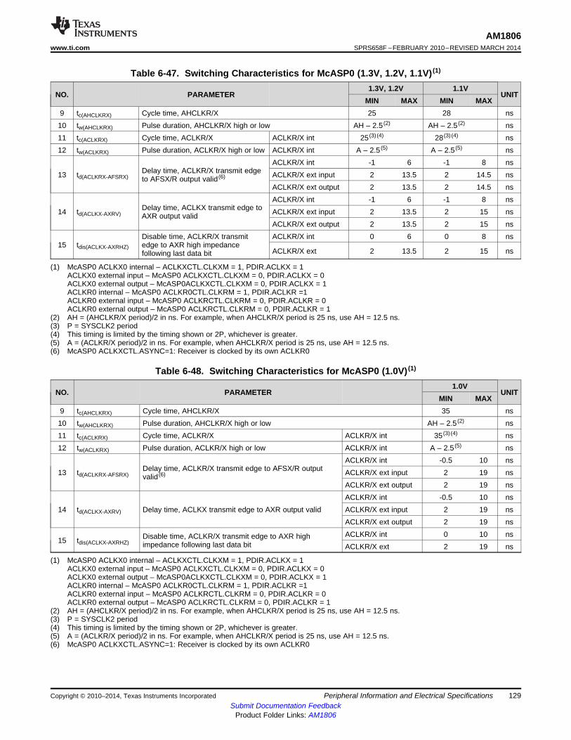
AM1806www.ti.com SPRS658F –FEBRUARY 2010–REVISED MARCH 2014
Table 6-47. Switching Characteristics for McASP0 (1.3V, 1.2V, 1.1V) (1)
1.3V, 1.2V 1.1VNO. PARAMETER UNIT
MIN MAX MIN MAX9 tc(AHCLKRX) Cycle time, AHCLKR/X 25 28 ns10 tw(AHCLKRX) Pulse duration, AHCLKR/X high or low AH – 2.5 (2) AH – 2.5 (2) ns11 tc(ACLKRX) Cycle time, ACLKR/X ACLKR/X int 25 (3) (4) 28 (3) (4) ns12 tw(ACLKRX) Pulse duration, ACLKR/X high or low ACLKR/X int A – 2.5 (5) A – 2.5 (5) ns
ACLKR/X int -1 6 -1 8 nsDelay time, ACLKR/X transmit edge13 td(ACLKRX-AFSRX) ACLKR/X ext input 2 13.5 2 14.5 nsto AFSX/R output valid (6)
ACLKR/X ext output 2 13.5 2 14.5 nsACLKR/X int -1 6 -1 8 ns
Delay time, ACLKX transmit edge to14 td(ACLKX-AXRV) ACLKR/X ext input 2 13.5 2 15 nsAXR output validACLKR/X ext output 2 13.5 2 15 ns
Disable time, ACLKR/X transmit ACLKR/X int 0 6 0 8 ns15 tdis(ACLKX-AXRHZ) edge to AXR high impedance
ACLKR/X ext 2 13.5 2 15 nsfollowing last data bit
(1) McASP0 ACLKX0 internal – ACLKXCTL.CLKXM = 1, PDIR.ACLKX = 1ACLKX0 external input – McASP0 ACLKXCTL.CLKXM = 0, PDIR.ACLKX = 0ACLKX0 external output – McASP0ACLKXCTL.CLKXM = 0, PDIR.ACLKX = 1ACLKR0 internal – McASP0 ACLKR0CTL.CLKRM = 1, PDIR.ACLKR =1ACLKR0 external input – McASP0 ACLKRCTL.CLKRM = 0, PDIR.ACLKR = 0ACLKR0 external output – McASP0 ACLKRCTL.CLKRM = 0, PDIR.ACLKR = 1
(2) AH = (AHCLKR/X period)/2 in ns. For example, when AHCLKR/X period is 25 ns, use AH = 12.5 ns.(3) P = SYSCLK2 period(4) This timing is limited by the timing shown or 2P, whichever is greater.(5) A = (ACLKR/X period)/2 in ns. For example, when AHCLKR/X period is 25 ns, use AH = 12.5 ns.(6) McASP0 ACLKXCTL.ASYNC=1: Receiver is clocked by its own ACLKR0
Table 6-48. Switching Characteristics for McASP0 (1.0V) (1)
1.0VNO. PARAMETER UNIT
MIN MAX9 tc(AHCLKRX) Cycle time, AHCLKR/X 35 ns10 tw(AHCLKRX) Pulse duration, AHCLKR/X high or low AH – 2.5 (2) ns11 tc(ACLKRX) Cycle time, ACLKR/X ACLKR/X int 35 (3) (4) ns12 tw(ACLKRX) Pulse duration, ACLKR/X high or low ACLKR/X int A – 2.5 (5) ns
ACLKR/X int -0.5 10 nsDelay time, ACLKR/X transmit edge to AFSX/R output13 td(ACLKRX-AFSRX) ACLKR/X ext input 2 19 nsvalid (6)
ACLKR/X ext output 2 19 nsACLKR/X int -0.5 10 ns
14 td(ACLKX-AXRV) Delay time, ACLKX transmit edge to AXR output valid ACLKR/X ext input 2 19 nsACLKR/X ext output 2 19 nsACLKR/X int 0 10 nsDisable time, ACLKR/X transmit edge to AXR high15 tdis(ACLKX-AXRHZ) impedance following last data bit ACLKR/X ext 2 19 ns
(1) McASP0 ACLKX0 internal – ACLKXCTL.CLKXM = 1, PDIR.ACLKX = 1ACLKX0 external input – McASP0 ACLKXCTL.CLKXM = 0, PDIR.ACLKX = 0ACLKX0 external output – McASP0ACLKXCTL.CLKXM = 0, PDIR.ACLKX = 1ACLKR0 internal – McASP0 ACLKR0CTL.CLKRM = 1, PDIR.ACLKR =1ACLKR0 external input – McASP0 ACLKRCTL.CLKRM = 0, PDIR.ACLKR = 0ACLKR0 external output – McASP0 ACLKRCTL.CLKRM = 0, PDIR.ACLKR = 1
(2) AH = (AHCLKR/X period)/2 in ns. For example, when AHCLKR/X period is 25 ns, use AH = 12.5 ns.(3) P = SYSCLK2 period(4) This timing is limited by the timing shown or 2P, whichever is greater.(5) A = (ACLKR/X period)/2 in ns. For example, when AHCLKR/X period is 25 ns, use AH = 12.5 ns.(6) McASP0 ACLKXCTL.ASYNC=1: Receiver is clocked by its own ACLKR0
Copyright © 2010–2014, Texas Instruments Incorporated Peripheral Information and Electrical Specifications 129Submit Documentation Feedback
Product Folder Links: AM1806
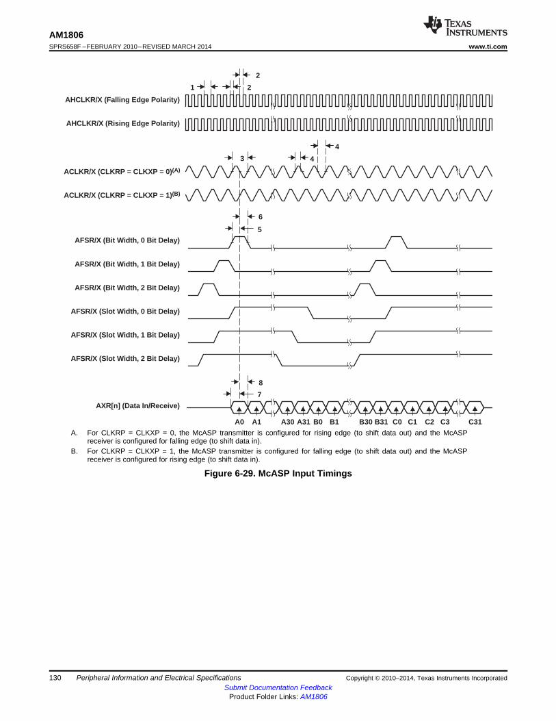
8
7
4
43
2
21
A0 A1 B0 B1A30 A31 B30 B31 C0 C1 C2 C3 C31
AHCLKR/X (Falling Edge Polarity)
AHCLKR/X (Rising Edge Polarity)
AFSR/X (Bit Width, 0 Bit Delay)
AFSR/X (Bit Width, 1 Bit Delay)
AFSR/X (Bit Width, 2 Bit Delay)
AFSR/X (Slot Width, 0 Bit Delay)
AFSR/X (Slot Width, 1 Bit Delay)
AFSR/X (Slot Width, 2 Bit Delay)
AXR[n] (Data In/Receive)
6
5
ACLKR/X (CLKRP = CLKXP = 0)(A)
ACLKR/X (CLKRP = CLKXP = 1)(B)
AM1806SPRS658F –FEBRUARY 2010–REVISED MARCH 2014 www.ti.com
A. For CLKRP = CLKXP = 0, the McASP transmitter is configured for rising edge (to shift data out) and the McASPreceiver is configured for falling edge (to shift data in).
B. For CLKRP = CLKXP = 1, the McASP transmitter is configured for falling edge (to shift data out) and the McASPreceiver is configured for rising edge (to shift data in).
Figure 6-29. McASP Input Timings
130 Peripheral Information and Electrical Specifications Copyright © 2010–2014, Texas Instruments IncorporatedSubmit Documentation Feedback
Product Folder Links: AM1806
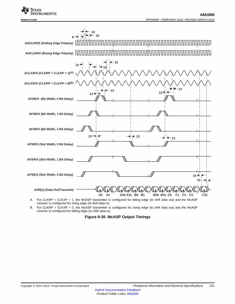
1514
131313
1313
1313
12
1211
1010
9
A0 A1 B0 B1A30 A31 B30 B31 C0 C1 C2 C3 C31
AHCLKR/X (Falling Edge Polarity)
AHCLKR/X (Rising Edge Polarity)
AFSR/X (Bit Width, 0 Bit Delay)
AFSR/X (Bit Width, 1 Bit Delay)
AFSR/X (Bit Width, 2 Bit Delay)
AFSR/X (Slot Width, 0 Bit Delay)
AFSR/X (Slot Width, 1 Bit Delay)
AFSR/X (Slot Width, 2 Bit Delay)
AXR[n] (Data Out/Transmit)
ACLKR/X (CLKRP = CLKXP = 0)(B)
ACLKR/X (CLKRP = CLKXP = 1)(A)
AM1806www.ti.com SPRS658F –FEBRUARY 2010–REVISED MARCH 2014
A. For CLKRP = CLKXP = 1, the McASP transmitter is configured for falling edge (to shift data out) and the McASPreceiver is configured for rising edge (to shift data in).
B. For CLKRP = CLKXP = 0, the McASP transmitter is configured for rising edge (to shift data out) and the McASPreceiver is configured for falling edge (to shift data in).
Figure 6-30. McASP Output Timings
Copyright © 2010–2014, Texas Instruments Incorporated Peripheral Information and Electrical Specifications 131Submit Documentation Feedback
Product Folder Links: AM1806

AM1806SPRS658F –FEBRUARY 2010–REVISED MARCH 2014 www.ti.com
6.15 Multichannel Buffered Serial Port (McBSP)The McBSP provides these functions:• Full-duplex communication• Double-buffered data registers, which allow a continuous data stream• Independent framing and clocking for receive and transmit• Direct interface to industry-standard codecs, analog interface chips (AICs), and other serially
connected analog-to-digital (A/D) and digital-to-analog (D/A) devices• External shift clock or an internal, programmable frequency shift clock for data transfer• Transmit & Receive FIFO Buffers allow the McBSP to operate at a higher sample rate by making it
more tolerant to DMA latency
If internal clock source is used, the CLKGDV field of the Sample Rate Generator Register (SRGR) mustalways be set to a value of 1 or greater.
6.15.1 McBSP Peripheral Register Description(s)
Table 6-49. McBSP/FIFO Registers
McBSP0 McBSP1 ACRONYM REGISTER DESCRIPTIONBYTE ADDRESS BYTE ADDRESSMcBSP Registers
0x01D1 0000 0x01D1 1000 DRR McBSP Data Receive Register (read-only)0x01D1 0004 0x01D1 1004 DXR McBSP Data Transmit Register0x01D1 0008 0x01D1 1008 SPCR McBSP Serial Port Control Register0x01D1 000C 0x01D1 100C RCR McBSP Receive Control Register0x01D1 0010 0x01D1 1010 XCR McBSP Transmit Control Register0x01D1 0014 0x01D1 1014 SRGR McBSP Sample Rate Generator register0x01D1 0018 0x01D1 1018 MCR McBSP Multichannel Control Register0x01D1 001C 0x01D1 101C RCERE0 McBSP Enhanced Receive Channel Enable Register 0 Partition A/B0x01D1 0020 0x01D1 1020 XCERE0 McBSP Enhanced Transmit Channel Enable Register 0 Partition A/B0x01D1 0024 0x01D1 1024 PCR McBSP Pin Control Register0x01D1 0028 0x01D1 1028 RCERE1 McBSP Enhanced Receive Channel Enable Register 1 Partition C/D0x01D1 002C 0x01D1 102C XCERE1 McBSP Enhanced Transmit Channel Enable Register 1 Partition C/D0x01D1 0030 0x01D1 1030 RCERE2 McBSP Enhanced Receive Channel Enable Register 2 Partition E/F0x01D1 0034 0x01D1 1034 XCERE2 McBSP Enhanced Transmit Channel Enable Register 2 Partition E/F0x01D1 0038 0x01D1 1038 RCERE3 McBSP Enhanced Receive Channel Enable Register 3 Partition G/H0x01D1 003C 0x01D1 103C XCERE3 McBSP Enhanced Transmit Channel Enable Register 3 Partition G/H
McBSP FIFO Control and Status Registers0x01D1 0800 0x01D1 1800 BFIFOREV BFIFO Revision Identification Register0x01D1 0810 0x01D1 1810 WFIFOCTL Write FIFO Control Register0x01D1 0814 0x01D1 1814 WFIFOSTS Write FIFO Status Register0x01D1 0818 0x01D1 1818 RFIFOCTL Read FIFO Control Register0x01D1 081C 0x01D1 181C RFIFOSTS Read FIFO Status Register
McBSP FIFO Data Registers0x01F1 0000 0x01F1 1000 RBUF McBSP FIFO Receive Buffer0x01F1 0000 0x01F1 1000 XBUF McBSP FIFO Transmit Buffer
132 Peripheral Information and Electrical Specifications Copyright © 2010–2014, Texas Instruments IncorporatedSubmit Documentation Feedback
Product Folder Links: AM1806
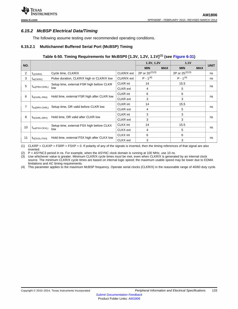
AM1806www.ti.com SPRS658F –FEBRUARY 2010–REVISED MARCH 2014
6.15.2 McBSP Electrical Data/TimingThe following assume testing over recommended operating conditions.
6.15.2.1 Multichannel Buffered Serial Port (McBSP) Timing
Table 6-50. Timing Requirements for McBSP0 [1.3V, 1.2V, 1.1V] (1) (see Figure 6-31)1.3V, 1.2V 1.1V
NO. UNITMIN MAX MIN MAX
2 tc(CKRX) Cycle time, CLKR/X CLKR/X ext 2P or 20 (2) (3) 2P or 25 (2) (3) ns3 tw(CKRX) Pulse duration, CLKR/X high or CLKR/X low CLKR/X ext P - 1 (4) P - 1 (4) ns
CLKR int 14 15.5Setup time, external FSR high before CLKR5 tsu(FRH-CKRL) nslow CLKR ext 4 5CLKR int 6 6
6 th(CKRL-FRH) Hold time, external FSR high after CLKR low nsCLKR ext 3 3CLKR int 14 15.5
7 tsu(DRV-CKRL) Setup time, DR valid before CLKR low nsCLKR ext 4 5CLKR int 3 3
8 th(CKRL-DRV) Hold time, DR valid after CLKR low nsCLKR ext 3 3CLKX int 14 15.5Setup time, external FSX high before CLKX10 tsu(FXH-CKXL) nslow CLKX ext 4 5CLKX int 6 6
11 th(CKXL-FXH) Hold time, external FSX high after CLKX low nsCLKX ext 3 3
(1) CLKRP = CLKXP = FSRP = FSXP = 0. If polarity of any of the signals is inverted, then the timing references of that signal are alsoinverted.
(2) P = ASYNC3 period in ns. For example, when the ASYNC clock domain is running at 100 MHz, use 10 ns.(3) Use whichever value is greater. Minimum CLKR/X cycle times must be met, even when CLKR/X is generated by an internal clock
source. The minimum CLKR/X cycle times are based on internal logic speed; the maximum usable speed may be lower due to EDMAlimitations and AC timing requirements.
(4) This parameter applies to the maximum McBSP frequency. Operate serial clocks (CLKR/X) in the reasonable range of 40/60 duty cycle.
Copyright © 2010–2014, Texas Instruments Incorporated Peripheral Information and Electrical Specifications 133Submit Documentation Feedback
Product Folder Links: AM1806
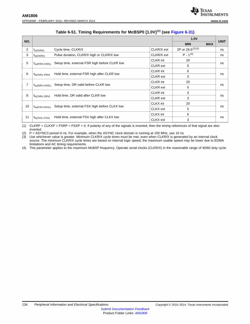
AM1806SPRS658F –FEBRUARY 2010–REVISED MARCH 2014 www.ti.com
Table 6-51. Timing Requirements for McBSP0 [1.0V] (1) (see Figure 6-31)1.0V
NO. UNITMIN MAX
2 tc(CKRX) Cycle time, CLKR/X CLKR/X ext 2P or 26.6 (2) (3) ns3 tw(CKRX) Pulse duration, CLKR/X high or CLKR/X low CLKR/X ext P - 1 (4) ns
CLKR int 205 tsu(FRH-CKRL) Setup time, external FSR high before CLKR low ns
CLKR ext 5CLKR int 6
6 th(CKRL-FRH) Hold time, external FSR high after CLKR low nsCLKR ext 3CLKR int 20
7 tsu(DRV-CKRL) Setup time, DR valid before CLKR low nsCLKR ext 5CLKR int 3
8 th(CKRL-DRV) Hold time, DR valid after CLKR low nsCLKR ext 3CLKX int 20
10 tsu(FXH-CKXL) Setup time, external FSX high before CLKX low nsCLKX ext 5CLKX int 6
11 th(CKXL-FXH) Hold time, external FSX high after CLKX low nsCLKX ext 3
(1) CLKRP = CLKXP = FSRP = FSXP = 0. If polarity of any of the signals is inverted, then the timing references of that signal are alsoinverted.
(2) P = ASYNC3 period in ns. For example, when the ASYNC clock domain is running at 100 MHz, use 10 ns.(3) Use whichever value is greater. Minimum CLKR/X cycle times must be met, even when CLKR/X is generated by an internal clock
source. The minimum CLKR/X cycle times are based on internal logic speed; the maximum usable speed may be lower due to EDMAlimitations and AC timing requirements.
(4) This parameter applies to the maximum McBSP frequency. Operate serial clocks (CLKR/X) in the reasonable range of 40/60 duty cycle.
134 Peripheral Information and Electrical Specifications Copyright © 2010–2014, Texas Instruments IncorporatedSubmit Documentation Feedback
Product Folder Links: AM1806
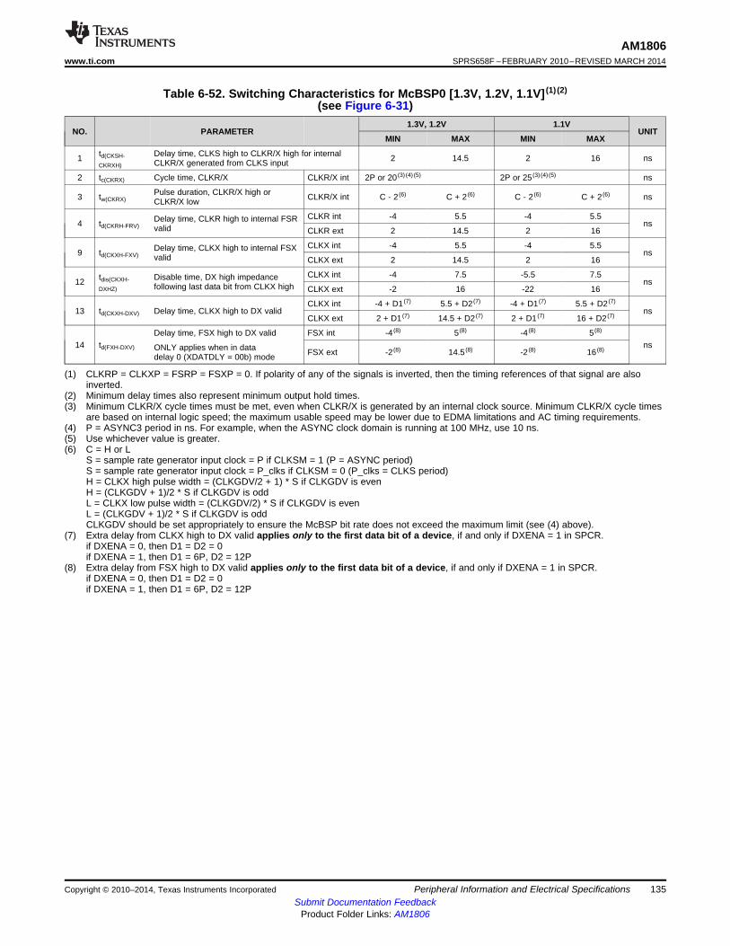
AM1806www.ti.com SPRS658F –FEBRUARY 2010–REVISED MARCH 2014
Table 6-52. Switching Characteristics for McBSP0 [1.3V, 1.2V, 1.1V] (1) (2)
(see Figure 6-31)1.3V, 1.2V 1.1V
NO. PARAMETER UNITMIN MAX MIN MAX
td(CKSH- Delay time, CLKS high to CLKR/X high for internal1 2 14.5 2 16 nsCKRXH) CLKR/X generated from CLKS input
2 tc(CKRX) Cycle time, CLKR/X CLKR/X int 2P or 20 (3) (4) (5) 2P or 25 (3) (4) (5) ns
Pulse duration, CLKR/X high or3 tw(CKRX) CLKR/X int C - 2 (6) C + 2 (6) C - 2 (6) C + 2 (6) nsCLKR/X low
CLKR int -4 5.5 -4 5.5Delay time, CLKR high to internal FSR4 td(CKRH-FRV) nsvalid CLKR ext 2 14.5 2 16
CLKX int -4 5.5 -4 5.5Delay time, CLKX high to internal FSX9 td(CKXH-FXV) nsvalid CLKX ext 2 14.5 2 16
CLKX int -4 7.5 -5.5 7.5tdis(CKXH- Disable time, DX high impedance12 nsDXHZ) following last data bit from CLKX high CLKX ext -2 16 -22 16
CLKX int -4 + D1 (7) 5.5 + D2 (7) -4 + D1 (7) 5.5 + D2 (7)
13 td(CKXH-DXV) Delay time, CLKX high to DX valid nsCLKX ext 2 + D1 (7) 14.5 + D2 (7) 2 + D1 (7) 16 + D2 (7)
Delay time, FSX high to DX valid FSX int -4 (8) 5 (8) -4 (8) 5 (8)
14 td(FXH-DXV) nsONLY applies when in data FSX ext -2 (8) 14.5 (8) -2 (8) 16 (8)delay 0 (XDATDLY = 00b) mode
(1) CLKRP = CLKXP = FSRP = FSXP = 0. If polarity of any of the signals is inverted, then the timing references of that signal are alsoinverted.
(2) Minimum delay times also represent minimum output hold times.(3) Minimum CLKR/X cycle times must be met, even when CLKR/X is generated by an internal clock source. Minimum CLKR/X cycle times
are based on internal logic speed; the maximum usable speed may be lower due to EDMA limitations and AC timing requirements.(4) P = ASYNC3 period in ns. For example, when the ASYNC clock domain is running at 100 MHz, use 10 ns.(5) Use whichever value is greater.(6) C = H or L
S = sample rate generator input clock = P if CLKSM = 1 (P = ASYNC period)S = sample rate generator input clock = P_clks if CLKSM = 0 (P_clks = CLKS period)H = CLKX high pulse width = (CLKGDV/2 + 1) * S if CLKGDV is evenH = (CLKGDV + 1)/2 * S if CLKGDV is oddL = CLKX low pulse width = (CLKGDV/2) * S if CLKGDV is evenL = (CLKGDV + 1)/2 * S if CLKGDV is oddCLKGDV should be set appropriately to ensure the McBSP bit rate does not exceed the maximum limit (see (4) above).
(7) Extra delay from CLKX high to DX valid applies only to the first data bit of a device, if and only if DXENA = 1 in SPCR.if DXENA = 0, then D1 = D2 = 0if DXENA = 1, then D1 = 6P, D2 = 12P
(8) Extra delay from FSX high to DX valid applies only to the first data bit of a device, if and only if DXENA = 1 in SPCR.if DXENA = 0, then D1 = D2 = 0if DXENA = 1, then D1 = 6P, D2 = 12P
Copyright © 2010–2014, Texas Instruments Incorporated Peripheral Information and Electrical Specifications 135Submit Documentation Feedback
Product Folder Links: AM1806
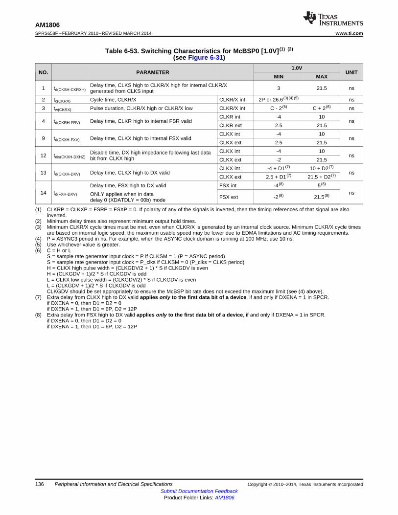
AM1806SPRS658F –FEBRUARY 2010–REVISED MARCH 2014 www.ti.com
Table 6-53. Switching Characteristics for McBSP0 [1.0V] (1) (2)
(see Figure 6-31)1.0V
NO. PARAMETER UNITMIN MAX
Delay time, CLKS high to CLKR/X high for internal CLKR/X1 td(CKSH-CKRXH) 3 21.5 nsgenerated from CLKS input2 tc(CKRX) Cycle time, CLKR/X CLKR/X int 2P or 26.6 (3) (4) (5) ns3 tw(CKRX) Pulse duration, CLKR/X high or CLKR/X low CLKR/X int C - 2 (6) C + 2 (6) ns
CLKR int -4 104 td(CKRH-FRV) Delay time, CLKR high to internal FSR valid ns
CLKR ext 2.5 21.5CLKX int -4 10
9 td(CKXH-FXV) Delay time, CLKX high to internal FSX valid nsCLKX ext 2.5 21.5CLKX int -4 10Disable time, DX high impedance following last data12 tdis(CKXH-DXHZ) nsbit from CLKX high CLKX ext -2 21.5CLKX int -4 + D1 (7) 10 + D2 (7)
13 td(CKXH-DXV) Delay time, CLKX high to DX valid nsCLKX ext 2.5 + D1 (7) 21.5 + D2 (7)
Delay time, FSX high to DX valid FSX int -4 (8) 5 (8)
14 td(FXH-DXV) nsONLY applies when in data FSX ext -2 (8) 21.5 (8)delay 0 (XDATDLY = 00b) mode
(1) CLKRP = CLKXP = FSRP = FSXP = 0. If polarity of any of the signals is inverted, then the timing references of that signal are alsoinverted.
(2) Minimum delay times also represent minimum output hold times.(3) Minimum CLKR/X cycle times must be met, even when CLKR/X is generated by an internal clock source. Minimum CLKR/X cycle times
are based on internal logic speed; the maximum usable speed may be lower due to EDMA limitations and AC timing requirements.(4) P = ASYNC3 period in ns. For example, when the ASYNC clock domain is running at 100 MHz, use 10 ns.(5) Use whichever value is greater.(6) C = H or L
S = sample rate generator input clock = P if CLKSM = 1 (P = ASYNC period)S = sample rate generator input clock = P_clks if CLKSM = 0 (P_clks = CLKS period)H = CLKX high pulse width = (CLKGDV/2 + 1) * S if CLKGDV is evenH = (CLKGDV + 1)/2 * S if CLKGDV is oddL = CLKX low pulse width = (CLKGDV/2) * S if CLKGDV is evenL = (CLKGDV + 1)/2 * S if CLKGDV is oddCLKGDV should be set appropriately to ensure the McBSP bit rate does not exceed the maximum limit (see (4) above).
(7) Extra delay from CLKX high to DX valid applies only to the first data bit of a device, if and only if DXENA = 1 in SPCR.if DXENA = 0, then D1 = D2 = 0if DXENA = 1, then D1 = 6P, D2 = 12P
(8) Extra delay from FSX high to DX valid applies only to the first data bit of a device, if and only if DXENA = 1 in SPCR.if DXENA = 0, then D1 = D2 = 0if DXENA = 1, then D1 = 6P, D2 = 12P
136 Peripheral Information and Electrical Specifications Copyright © 2010–2014, Texas Instruments IncorporatedSubmit Documentation Feedback
Product Folder Links: AM1806
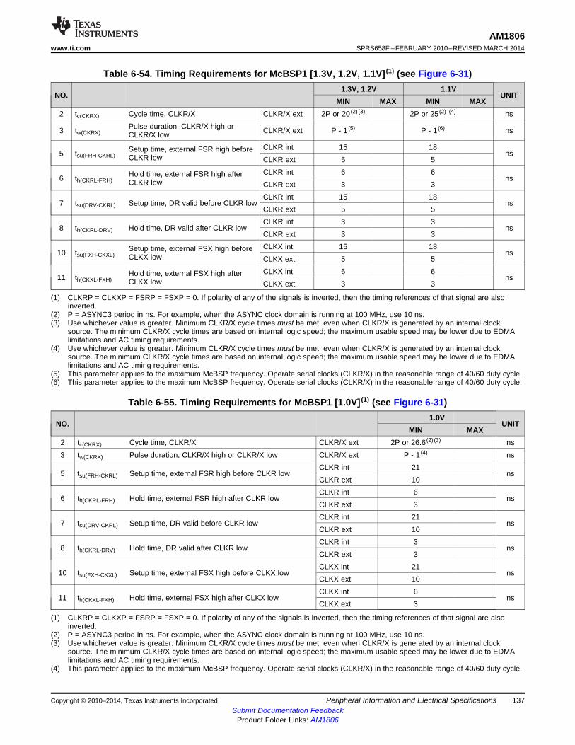
AM1806www.ti.com SPRS658F –FEBRUARY 2010–REVISED MARCH 2014
Table 6-54. Timing Requirements for McBSP1 [1.3V, 1.2V, 1.1V] (1) (see Figure 6-31)1.3V, 1.2V 1.1V
NO. UNITMIN MAX MIN MAX
2 tc(CKRX) Cycle time, CLKR/X CLKR/X ext 2P or 20 (2) (3) 2P or 25 (2) (4) nsPulse duration, CLKR/X high or3 tw(CKRX) CLKR/X ext P - 1 (5) P - 1 (6) nsCLKR/X low
CLKR int 15 18Setup time, external FSR high before5 tsu(FRH-CKRL) nsCLKR low CLKR ext 5 5CLKR int 6 6Hold time, external FSR high after6 th(CKRL-FRH) nsCLKR low CLKR ext 3 3CLKR int 15 18
7 tsu(DRV-CKRL) Setup time, DR valid before CLKR low nsCLKR ext 5 5CLKR int 3 3
8 th(CKRL-DRV) Hold time, DR valid after CLKR low nsCLKR ext 3 3CLKX int 15 18Setup time, external FSX high before10 tsu(FXH-CKXL) nsCLKX low CLKX ext 5 5CLKX int 6 6Hold time, external FSX high after11 th(CKXL-FXH) nsCLKX low CLKX ext 3 3
(1) CLKRP = CLKXP = FSRP = FSXP = 0. If polarity of any of the signals is inverted, then the timing references of that signal are alsoinverted.
(2) P = ASYNC3 period in ns. For example, when the ASYNC clock domain is running at 100 MHz, use 10 ns.(3) Use whichever value is greater. Minimum CLKR/X cycle times must be met, even when CLKR/X is generated by an internal clock
source. The minimum CLKR/X cycle times are based on internal logic speed; the maximum usable speed may be lower due to EDMAlimitations and AC timing requirements.
(4) Use whichever value is greater. Minimum CLKR/X cycle times must be met, even when CLKR/X is generated by an internal clocksource. The minimum CLKR/X cycle times are based on internal logic speed; the maximum usable speed may be lower due to EDMAlimitations and AC timing requirements.
(5) This parameter applies to the maximum McBSP frequency. Operate serial clocks (CLKR/X) in the reasonable range of 40/60 duty cycle.(6) This parameter applies to the maximum McBSP frequency. Operate serial clocks (CLKR/X) in the reasonable range of 40/60 duty cycle.
Table 6-55. Timing Requirements for McBSP1 [1.0V] (1) (see Figure 6-31)1.0V
NO. UNITMIN MAX
2 tc(CKRX) Cycle time, CLKR/X CLKR/X ext 2P or 26.6 (2) (3) ns3 tw(CKRX) Pulse duration, CLKR/X high or CLKR/X low CLKR/X ext P - 1 (4) ns
CLKR int 215 tsu(FRH-CKRL) Setup time, external FSR high before CLKR low ns
CLKR ext 10CLKR int 6
6 th(CKRL-FRH) Hold time, external FSR high after CLKR low nsCLKR ext 3CLKR int 21
7 tsu(DRV-CKRL) Setup time, DR valid before CLKR low nsCLKR ext 10CLKR int 3
8 th(CKRL-DRV) Hold time, DR valid after CLKR low nsCLKR ext 3CLKX int 21
10 tsu(FXH-CKXL) Setup time, external FSX high before CLKX low nsCLKX ext 10CLKX int 6
11 th(CKXL-FXH) Hold time, external FSX high after CLKX low nsCLKX ext 3
(1) CLKRP = CLKXP = FSRP = FSXP = 0. If polarity of any of the signals is inverted, then the timing references of that signal are alsoinverted.
(2) P = ASYNC3 period in ns. For example, when the ASYNC clock domain is running at 100 MHz, use 10 ns.(3) Use whichever value is greater. Minimum CLKR/X cycle times must be met, even when CLKR/X is generated by an internal clock
source. The minimum CLKR/X cycle times are based on internal logic speed; the maximum usable speed may be lower due to EDMAlimitations and AC timing requirements.
(4) This parameter applies to the maximum McBSP frequency. Operate serial clocks (CLKR/X) in the reasonable range of 40/60 duty cycle.
Copyright © 2010–2014, Texas Instruments Incorporated Peripheral Information and Electrical Specifications 137Submit Documentation Feedback
Product Folder Links: AM1806
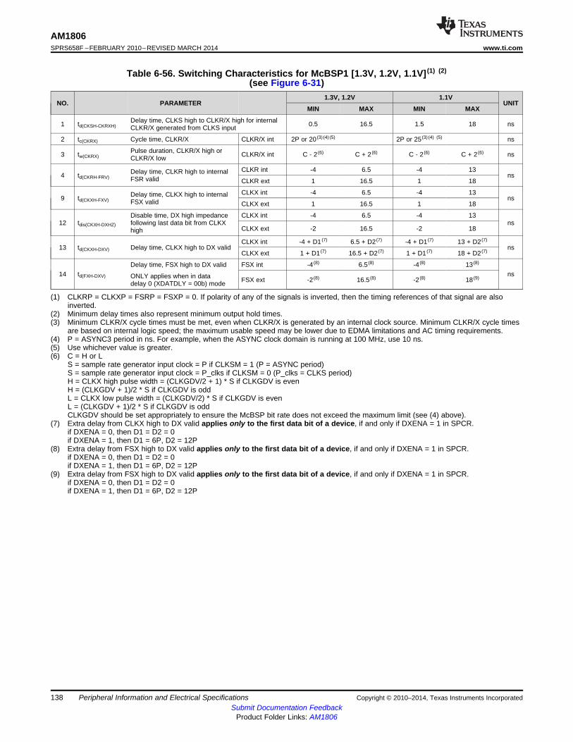
AM1806SPRS658F –FEBRUARY 2010–REVISED MARCH 2014 www.ti.com
Table 6-56. Switching Characteristics for McBSP1 [1.3V, 1.2V, 1.1V] (1) (2)
(see Figure 6-31)1.3V, 1.2V 1.1V
NO. PARAMETER UNITMIN MAX MIN MAX
Delay time, CLKS high to CLKR/X high for internal1 td(CKSH-CKRXH) 0.5 16.5 1.5 18 nsCLKR/X generated from CLKS input
2 tc(CKRX) Cycle time, CLKR/X CLKR/X int 2P or 20 (3) (4) (5) 2P or 25 (3) (4) (5) ns
Pulse duration, CLKR/X high or3 tw(CKRX) CLKR/X int C - 2 (6) C + 2 (6) C - 2 (6) C + 2 (6) nsCLKR/X low
CLKR int -4 6.5 -4 13Delay time, CLKR high to internal4 td(CKRH-FRV) nsFSR valid CLKR ext 1 16.5 1 18
CLKX int -4 6.5 -4 13Delay time, CLKX high to internal9 td(CKXH-FXV) nsFSX valid CLKX ext 1 16.5 1 18
Disable time, DX high impedance CLKX int -4 6.5 -4 1312 tdis(CKXH-DXHZ) following last data bit from CLKX ns
CLKX ext -2 16.5 -2 18high
CLKX int -4 + D1 (7) 6.5 + D2 (7) -4 + D1 (7) 13 + D2 (7)
13 td(CKXH-DXV) Delay time, CLKX high to DX valid nsCLKX ext 1 + D1 (7) 16.5 + D2 (7) 1 + D1 (7) 18 + D2 (7)
Delay time, FSX high to DX valid FSX int -4 (8) 6.5 (8) -4 (8) 13 (8)
14 td(FXH-DXV) nsONLY applies when in data FSX ext -2 (8) 16.5 (8) -2 (8) 18 (9)delay 0 (XDATDLY = 00b) mode
(1) CLKRP = CLKXP = FSRP = FSXP = 0. If polarity of any of the signals is inverted, then the timing references of that signal are alsoinverted.
(2) Minimum delay times also represent minimum output hold times.(3) Minimum CLKR/X cycle times must be met, even when CLKR/X is generated by an internal clock source. Minimum CLKR/X cycle times
are based on internal logic speed; the maximum usable speed may be lower due to EDMA limitations and AC timing requirements.(4) P = ASYNC3 period in ns. For example, when the ASYNC clock domain is running at 100 MHz, use 10 ns.(5) Use whichever value is greater.(6) C = H or L
S = sample rate generator input clock = P if CLKSM = 1 (P = ASYNC period)S = sample rate generator input clock = P_clks if CLKSM = 0 (P_clks = CLKS period)H = CLKX high pulse width = (CLKGDV/2 + 1) * S if CLKGDV is evenH = (CLKGDV + 1)/2 * S if CLKGDV is oddL = CLKX low pulse width = (CLKGDV/2) * S if CLKGDV is evenL = (CLKGDV + 1)/2 * S if CLKGDV is oddCLKGDV should be set appropriately to ensure the McBSP bit rate does not exceed the maximum limit (see (4) above).
(7) Extra delay from CLKX high to DX valid applies only to the first data bit of a device, if and only if DXENA = 1 in SPCR.if DXENA = 0, then D1 = D2 = 0if DXENA = 1, then D1 = 6P, D2 = 12P
(8) Extra delay from FSX high to DX valid applies only to the first data bit of a device, if and only if DXENA = 1 in SPCR.if DXENA = 0, then D1 = D2 = 0if DXENA = 1, then D1 = 6P, D2 = 12P
(9) Extra delay from FSX high to DX valid applies only to the first data bit of a device, if and only if DXENA = 1 in SPCR.if DXENA = 0, then D1 = D2 = 0if DXENA = 1, then D1 = 6P, D2 = 12P
138 Peripheral Information and Electrical Specifications Copyright © 2010–2014, Texas Instruments IncorporatedSubmit Documentation Feedback
Product Folder Links: AM1806
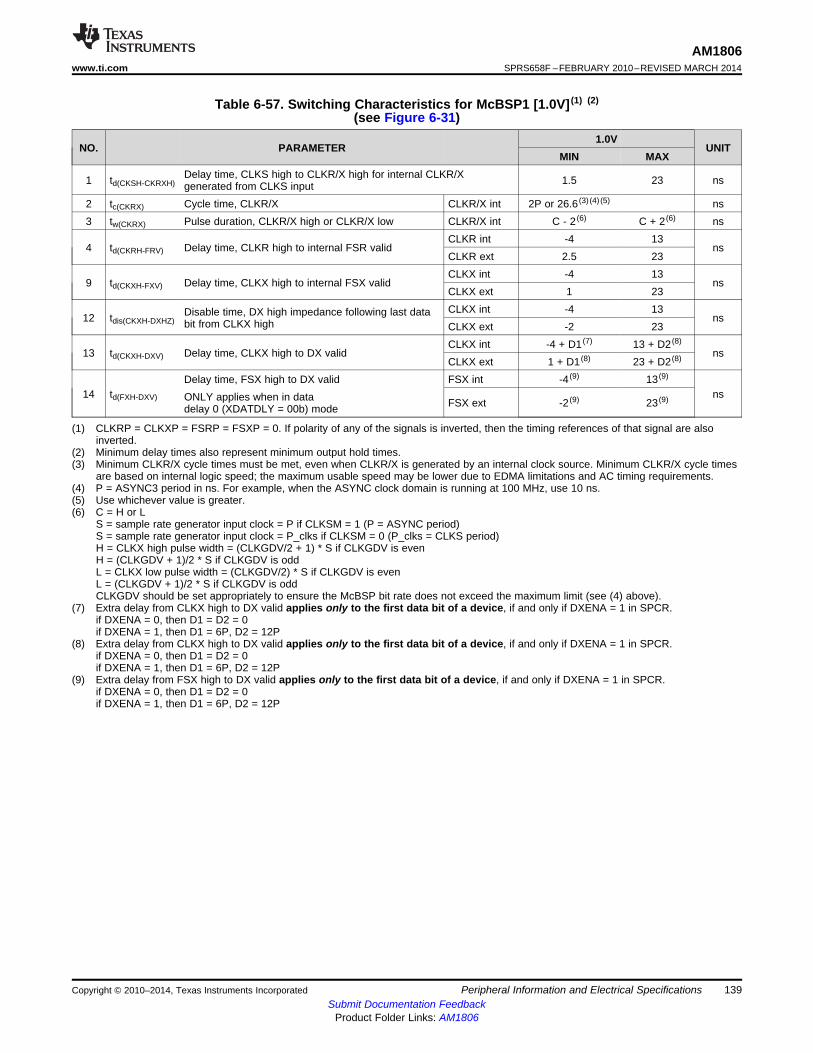
AM1806www.ti.com SPRS658F –FEBRUARY 2010–REVISED MARCH 2014
Table 6-57. Switching Characteristics for McBSP1 [1.0V] (1) (2)
(see Figure 6-31)1.0V
NO. PARAMETER UNITMIN MAX
Delay time, CLKS high to CLKR/X high for internal CLKR/X1 td(CKSH-CKRXH) 1.5 23 nsgenerated from CLKS input2 tc(CKRX) Cycle time, CLKR/X CLKR/X int 2P or 26.6 (3) (4) (5) ns3 tw(CKRX) Pulse duration, CLKR/X high or CLKR/X low CLKR/X int C - 2 (6) C + 2 (6) ns
CLKR int -4 134 td(CKRH-FRV) Delay time, CLKR high to internal FSR valid ns
CLKR ext 2.5 23CLKX int -4 13
9 td(CKXH-FXV) Delay time, CLKX high to internal FSX valid nsCLKX ext 1 23CLKX int -4 13Disable time, DX high impedance following last data12 tdis(CKXH-DXHZ) nsbit from CLKX high CLKX ext -2 23CLKX int -4 + D1 (7) 13 + D2 (8)
13 td(CKXH-DXV) Delay time, CLKX high to DX valid nsCLKX ext 1 + D1 (8) 23 + D2 (8)
Delay time, FSX high to DX valid FSX int -4 (9) 13 (9)
14 td(FXH-DXV) nsONLY applies when in data FSX ext -2 (9) 23 (9)delay 0 (XDATDLY = 00b) mode
(1) CLKRP = CLKXP = FSRP = FSXP = 0. If polarity of any of the signals is inverted, then the timing references of that signal are alsoinverted.
(2) Minimum delay times also represent minimum output hold times.(3) Minimum CLKR/X cycle times must be met, even when CLKR/X is generated by an internal clock source. Minimum CLKR/X cycle times
are based on internal logic speed; the maximum usable speed may be lower due to EDMA limitations and AC timing requirements.(4) P = ASYNC3 period in ns. For example, when the ASYNC clock domain is running at 100 MHz, use 10 ns.(5) Use whichever value is greater.(6) C = H or L
S = sample rate generator input clock = P if CLKSM = 1 (P = ASYNC period)S = sample rate generator input clock = P_clks if CLKSM = 0 (P_clks = CLKS period)H = CLKX high pulse width = (CLKGDV/2 + 1) * S if CLKGDV is evenH = (CLKGDV + 1)/2 * S if CLKGDV is oddL = CLKX low pulse width = (CLKGDV/2) * S if CLKGDV is evenL = (CLKGDV + 1)/2 * S if CLKGDV is oddCLKGDV should be set appropriately to ensure the McBSP bit rate does not exceed the maximum limit (see (4) above).
(7) Extra delay from CLKX high to DX valid applies only to the first data bit of a device, if and only if DXENA = 1 in SPCR.if DXENA = 0, then D1 = D2 = 0if DXENA = 1, then D1 = 6P, D2 = 12P
(8) Extra delay from CLKX high to DX valid applies only to the first data bit of a device, if and only if DXENA = 1 in SPCR.if DXENA = 0, then D1 = D2 = 0if DXENA = 1, then D1 = 6P, D2 = 12P
(9) Extra delay from FSX high to DX valid applies only to the first data bit of a device, if and only if DXENA = 1 in SPCR.if DXENA = 0, then D1 = D2 = 0if DXENA = 1, then D1 = 6P, D2 = 12P
Copyright © 2010–2014, Texas Instruments Incorporated Peripheral Information and Electrical Specifications 139Submit Documentation Feedback
Product Folder Links: AM1806
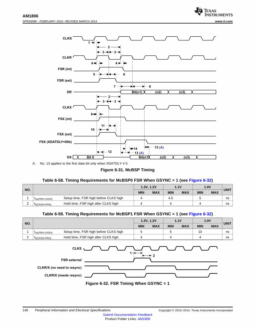
21
CLKS
FSR external
CLKR/X (no need to resync)
CLKR/X (needs resync)
Bit(n1) (n2) (n3)
Bit 0 Bit(n1) (n2) (n3)
1412
1110
9
33
2
87
65
44
3
1
3
2
CLKS
CLKR
FSR (int)
FSR (ext)
DR
CLKX
FSX (int)
FSX (ext)
FSX (XDATDLY=00b)
DX
13 (A)
13 (A)
AM1806SPRS658F –FEBRUARY 2010–REVISED MARCH 2014 www.ti.com
A. No. 13 applies to the first data bit only when XDATDLY ≠ 0.
Figure 6-31. McBSP Timing
Table 6-58. Timing Requirements for McBSP0 FSR When GSYNC = 1 (see Figure 6-32)1.3V, 1.2V 1.1V 1.0V
NO. UNITMIN MAX MIN MAX MIN MAX
1 tsu(FRH-CKSH) Setup time, FSR high before CLKS high 4 4.5 5 ns2 th(CKSH-FRH) Hold time, FSR high after CLKS high 4 4 4 ns
Table 6-59. Timing Requirements for McBSP1 FSR When GSYNC = 1 (see Figure 6-32)1.3V, 1.2V 1.1V 1.0V
NO. UNITMIN MAX MIN MAX MIN MAX
1 tsu(FRH-CKSH) Setup time, FSR high before CLKS high 5 5 10 ns2 th(CKSH-FRH) Hold time, FSR high after CLKS high 4 4 4 ns
Figure 6-32. FSR Timing When GSYNC = 1
140 Peripheral Information and Electrical Specifications Copyright © 2010–2014, Texas Instruments IncorporatedSubmit Documentation Feedback
Product Folder Links: AM1806
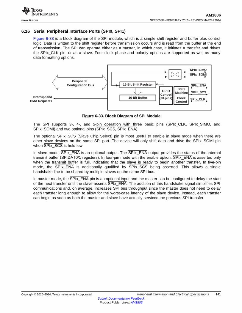
Peripheral Configuration Bus
Interrupt andDMA Requests
16-Bit Shift Register
16-Bit Buffer
GPIOControl(all pins)
StateMachine
ClockControl
SPIx_SIMO
SPIx_SOMI
SPIx_ENA
SPIx_SCS
SPIx_CLK
AM1806www.ti.com SPRS658F –FEBRUARY 2010–REVISED MARCH 2014
6.16 Serial Peripheral Interface Ports (SPI0, SPI1)Figure 6-33 is a block diagram of the SPI module, which is a simple shift register and buffer plus controllogic. Data is written to the shift register before transmission occurs and is read from the buffer at the endof transmission. The SPI can operate either as a master, in which case, it initiates a transfer and drivesthe SPIx_CLK pin, or as a slave. Four clock phase and polarity options are supported as well as manydata formatting options.
Figure 6-33. Block Diagram of SPI Module
The SPI supports 3-, 4-, and 5-pin operation with three basic pins (SPIx_CLK, SPIx_SIMO, andSPIx_SOMI) and two optional pins (SPIx_SCS, SPIx_ENA).
The optional SPIx_SCS (Slave Chip Select) pin is most useful to enable in slave mode when there areother slave devices on the same SPI port. The device will only shift data and drive the SPIx_SOMI pinwhen SPIx_SCS is held low.
In slave mode, SPIx_ENA is an optional output. The SPIx_ENA output provides the status of the internaltransmit buffer (SPIDAT0/1 registers). In four-pin mode with the enable option, SPIx_ENA is asserted onlywhen the transmit buffer is full, indicating that the slave is ready to begin another transfer. In five-pinmode, the SPIx_ENA is additionally qualified by SPIx_SCS being asserted. This allows a singlehandshake line to be shared by multiple slaves on the same SPI bus.
In master mode, the SPIx_ENA pin is an optional input and the master can be configured to delay the startof the next transfer until the slave asserts SPIx_ENA. The addition of this handshake signal simplifies SPIcommunications and, on average, increases SPI bus throughput since the master does not need to delayeach transfer long enough to allow for the worst-case latency of the slave device. Instead, each transfercan begin as soon as both the master and slave have actually serviced the previous SPI transfer.
Copyright © 2010–2014, Texas Instruments Incorporated Peripheral Information and Electrical Specifications 141Submit Documentation Feedback
Product Folder Links: AM1806

Optional − Slave Chip Select
Optional Enable (Ready)
SLAVE SPIMASTER SPI
SPIx_SIMOSPIx_SIMO
SPIx_SOMI SPIx_SOMI
SPIx_CLK SPIx_CLK
SPIx_ENA SPIx_ENA
SPIx_SCS SPIx_SCS
AM1806SPRS658F –FEBRUARY 2010–REVISED MARCH 2014 www.ti.com
Figure 6-34. Illustration of SPI Master-to-SPI Slave Connection
142 Peripheral Information and Electrical Specifications Copyright © 2010–2014, Texas Instruments IncorporatedSubmit Documentation Feedback
Product Folder Links: AM1806
AM1806www.ti.com SPRS658F –FEBRUARY 2010–REVISED MARCH 2014
6.16.1 SPI Peripheral Registers Description(s)Table 6-60 is a list of the SPI registers.
Table 6-60. SPIx Configuration Registers
SPI0 SPI1 ACRONYM DESCRIPTIONBYTE ADDRESS BYTE ADDRESS0x01C4 1000 0x01F0 E000 SPIGCR0 Global Control Register 00x01C4 1004 0x01F0 E004 SPIGCR1 Global Control Register 10x01C4 1008 0x01F0 E008 SPIINT0 Interrupt Register0x01C4 100C 0x01F0 E00C SPILVL Interrupt Level Register0x01C4 1010 0x01F0 E010 SPIFLG Flag Register0x01C4 1014 0x01F0 E014 SPIPC0 Pin Control Register 0 (Pin Function)0x01C4 1018 0x01F0 E018 SPIPC1 Pin Control Register 1 (Pin Direction)0x01C4 101C 0x01F0 E01C SPIPC2 Pin Control Register 2 (Pin Data In)0x01C4 1020 0x01F0 E020 SPIPC3 Pin Control Register 3 (Pin Data Out)0x01C4 1024 0x01F0 E024 SPIPC4 Pin Control Register 4 (Pin Data Set)0x01C4 1028 0x01F0 E028 SPIPC5 Pin Control Register 5 (Pin Data Clear)0x01C4 102C 0x01F0 E02C Reserved Reserved - Do not write to this register0x01C4 1030 0x01F0 E030 Reserved Reserved - Do not write to this register0x01C4 1034 0x01F0 E034 Reserved Reserved - Do not write to this register0x01C4 1038 0x01F0 E038 SPIDAT0 Shift Register 0 (without format select)0x01C4 103C 0x01F0 E03C SPIDAT1 Shift Register 1 (with format select)0x01C4 1040 0x01F0 E040 SPIBUF Buffer Register0x01C4 1044 0x01F0 E044 SPIEMU Emulation Register0x01C4 1048 0x01F0 E048 SPIDELAY Delay Register0x01C4 104C 0x01F0 E04C SPIDEF Default Chip Select Register0x01C4 1050 0x01F0 E050 SPIFMT0 Format Register 00x01C4 1054 0x01F0 E054 SPIFMT1 Format Register 10x01C4 1058 0x01F0 E058 SPIFMT2 Format Register 20x01C4 105C 0x01F0 E05C SPIFMT3 Format Register 30x01C4 1060 0x01F0 E060 INTVEC0 Interrupt Vector for SPI INT00x01C4 1064 0x01F0 E064 INTVEC1 Interrupt Vector for SPI INT1
Copyright © 2010–2014, Texas Instruments Incorporated Peripheral Information and Electrical Specifications 143Submit Documentation Feedback
Product Folder Links: AM1806
AM1806SPRS658F –FEBRUARY 2010–REVISED MARCH 2014 www.ti.com
6.16.2 SPI Electrical Data/Timing
6.16.2.1 Serial Peripheral Interface (SPI) Timing
Table 6-61 through Table 6-76 assume testing over recommended operating conditions (see Figure 6-35through Figure 6-38).
Table 6-61. General Timing Requirements for SPI0 Master Modes (1)
1.3V, 1.2V 1.1V 1.0VNO. UNIT
MIN MAX MIN MAX MIN MAX
1 tc(SPC)M Cycle Time, SPI0_CLK, All Master Modes 20 (2) 256P 30 (2) 256P 40 (2) 256P ns
2 tw(SPCH)M Pulse Width High, SPI0_CLK, All Master Modes 0.5M-1 0.5M-1 0.5M-1 ns
3 tw(SPCL)M Pulse Width Low, SPI0_CLK, All Master Modes 0.5M-1 0.5M-1 0.5M-1 ns
Polarity = 0, Phase = 0, 5 5 6to SPI0_CLK rising
Polarity = 0, Phase = 1, -0.5M+5 -0.5M+5 -0.5M+6Delay, initial data bit valid on to SPI0_CLK rising4 td(SIMO_SPC)M SPI0_SIMO after initial edge ns
Polarity = 1, Phase = 0,on SPI0_CLK (3)5 5 6to SPI0_CLK falling
Polarity = 1, Phase = 1, -0.5M+5 -0.5M+5 -0.5M+6to SPI0_CLK falling
Polarity = 0, Phase = 0, 5 5 6from SPI0_CLK rising
Polarity = 0, Phase = 1, 5 5 6Delay, subsequent bits valid from SPI0_CLK falling5 td(SPC_SIMO)M on SPI0_SIMO after transmit ns
Polarity = 1, Phase = 0,edge of SPI0_CLK 5 5 6from SPI0_CLK falling
Polarity = 1, Phase = 1, 5 5 6from SPI0_CLK rising
Polarity = 0, Phase = 0, 0.5M-3 0.5M-3 0.5M-3from SPI0_CLK falling
Polarity = 0, Phase = 1, 0.5M-3 0.5M-3 0.5M-3Output hold time, SPI0_SIMO from SPI0_CLK rising6 toh(SPC_SIMO)M valid after receive edge of ns
Polarity = 1, Phase = 0,SPI0_CLK 0.5M-3 0.5M-3 0.5M-3from SPI0_CLK rising
Polarity = 1, Phase = 1, 0.5M-3 0.5M-3 0.5M-3from SPI0_CLK falling
Polarity = 0, Phase = 0, 1.5 1.5 1.5to SPI0_CLK falling
Polarity = 0, Phase = 1, 1.5 1.5 1.5Input Setup Time, SPI0_SOMI to SPI0_CLK rising7 tsu(SOMI_SPC)M valid before receive edge of ns
Polarity = 1, Phase = 0,SPI0_CLK 1.5 1.5 1.5to SPI0_CLK rising
Polarity = 1, Phase = 1, 1.5 1.5 1.5to SPI0_CLK falling
Polarity = 0, Phase = 0, 4 4 5from SPI0_CLK falling
Polarity = 0, Phase = 1, 4 4 5Input Hold Time, SPI0_SOMI from SPI0_CLK rising8 tih(SPC_SOMI)M valid after receive edge of ns
Polarity = 1, Phase = 0,SPI0_CLK 4 4 5from SPI0_CLK rising
Polarity = 1, Phase = 1, 4 4 5from SPI0_CLK falling
(1) P = SYSCLK2 period; M = tc(SPC)M (SPI master bit clock period)(2) This timing is limited by the timing shown or 3P, whichever is greater.(3) First bit may be MSB or LSB depending upon SPI configuration. MO(0) refers to first bit and MO(n) refers to last bit output on
SPI0_SIMO. MI(0) refers to the first bit input and MI(n) refers to the last bit input on SPI0_SOMI.
144 Peripheral Information and Electrical Specifications Copyright © 2010–2014, Texas Instruments IncorporatedSubmit Documentation Feedback
Product Folder Links: AM1806

AM1806www.ti.com SPRS658F –FEBRUARY 2010–REVISED MARCH 2014
Table 6-62. General Timing Requirements for SPI0 Slave Modes (1)
1.3V, 1.2V 1.1V 1.0VNO. UNIT
MIN MAX MIN MAX MIN MAX9 tc(SPC)S Cycle Time, SPI0_CLK, All Slave Modes 40 (2) 50 (2) 60 (2) ns10 tw(SPCH)S Pulse Width High, SPI0_CLK, All Slave Modes 18 22 27 ns11 tw(SPCL)S Pulse Width Low, SPI0_CLK, All Slave Modes 18 22 27 ns
Polarity = 0, Phase = 0, 2P 2P 2Pto SPI0_CLK risingPolarity = 0, Phase = 1,Setup time, transmit data 2P 2P 2Pto SPI0_CLK risingwritten to SPI before initial12 tsu(SOMI_SPC)S nsclock edge from Polarity = 1, Phase = 0, 2P 2P 2Pmaster. (3) (4) to SPI0_CLK fallingPolarity = 1, Phase = 1, 2P 2P 2Pto SPI0_CLK fallingPolarity = 0, Phase = 0, 17 20 27from SPI0_CLK risingPolarity = 0, Phase = 1, 17 20 27Delay, subsequent bits valid from SPI0_CLK falling
13 td(SPC_SOMI)S on SPI0_SOMI after nsPolarity = 1, Phase = 0,transmit edge of SPI0_CLK 17 20 27from SPI0_CLK fallingPolarity = 1, Phase = 1, 17 20 27from SPI0_CLK risingPolarity = 0, Phase = 0, 0.5S-6 0.5S-16 0.5S-20from SPI0_CLK fallingPolarity = 0, Phase = 1, 0.5S-6 0.5S-16 0.5S-20Output hold time, from SPI0_CLK rising
14 toh(SPC_SOMI)S SPI0_SOMI valid after nsPolarity = 1, Phase = 0,receive edge of SPI0_CLK 0.5S-6 0.5S-16 0.5S-20from SPI0_CLK risingPolarity = 1, Phase = 1, 0.5S-6 0.5S-16 0.5S-20from SPI0_CLK fallingPolarity = 0, Phase = 0, 1.5 1.5 1.5to SPI0_CLK fallingPolarity = 0, Phase = 1, 1.5 1.5 1.5Input Setup Time, to SPI0_CLK rising
15 tsu(SIMO_SPC)S SPI0_SIMO valid before nsPolarity = 1, Phase = 0,receive edge of SPI0_CLK 1.5 1.5 1.5to SPI0_CLK risingPolarity = 1, Phase = 1, 1.5 1.5 1.5to SPI0_CLK fallingPolarity = 0, Phase = 0, 4 4 5from SPI0_CLK fallingPolarity = 0, Phase = 1, 4 4 5Input Hold Time, from SPI0_CLK rising
16 tih(SPC_SIMO)S SPI0_SIMO valid after nsPolarity = 1, Phase = 0,receive edge of SPI0_CLK 4 4 5from SPI0_CLK risingPolarity = 1, Phase = 1, 4 4 5from SPI0_CLK falling
(1) P = SYSCLK2 period; S = tc(SPC)S (SPI slave bit clock period)(2) This timing is limited by the timing shown or 3P, whichever is greater.(3) First bit may be MSB or LSB depending upon SPI configuration. SO(0) refers to first bit and SO(n) refers to last bit output on
SPI0_SOMI. SI(0) refers to the first bit input and SI(n) refers to the last bit input on SPI0_SIMO.(4) Measured from the termination of the write of new data to the SPI module, In analyzing throughput requirements, additional internal bus
cycles must be accounted for to allow data to be written to the SPI module by the CPU.
Copyright © 2010–2014, Texas Instruments Incorporated Peripheral Information and Electrical Specifications 145Submit Documentation Feedback
Product Folder Links: AM1806
AM1806SPRS658F –FEBRUARY 2010–REVISED MARCH 2014 www.ti.com
Table 6-63. Additional SPI0 Master Timings, 4-Pin Enable Option (1) (2) (3)
1.3V, 1.2V 1.1V 1.0VNO. PARAMETER UNIT
MIN MAX MIN MAX MIN MAXPolarity = 0, Phase = 0, 3P+5 3P+5 3P+6to SPI0_CLK risingPolarity = 0, Phase = 1, 0.5M+3P+5 0.5M+3P+5 0.5M+3P+6to SPI0_CLK risingDelay from slave assertion of SPI0_ENA17 td(ENA_SPC)M nsactive to first SPI0_CLK from master. (4) Polarity = 1, Phase = 0, 3P+5 3P+5 3P+6to SPI0_CLK fallingPolarity = 1, Phase = 1, 0.5M+3P+5 0.5M+3P+5 0.5M+3P+6to SPI0_CLK fallingPolarity = 0, Phase = 0, 0.5M+P+5 0.5M+P+5 0.5M+P+6from SPI0_CLK fallingPolarity = 0, Phase = 1, P+5 P+5 P+6Max delay for slave to deassert SPI0_ENA from SPI0_CLK falling
18 td(SPC_ENA)M after final SPI0_CLK edge to ensure nsPolarity = 1, Phase = 0,master does not begin the next transfer. (5) 0.5M+P+5 0.5M+P+5 0.5M+P+6from SPI0_CLK risingPolarity = 1, Phase = 1, P+5 P+5 P+6from SPI0_CLK rising
(1) These parameters are in addition to the general timings for SPI master modes (Table 6-61).(2) P = SYSCLK2 period; M = tc(SPC)M (SPI master bit clock period)(3) Figure shows only Polarity = 0, Phase = 0 as an example. Table gives parameters for all four master clocking modes.(4) In the case where the master SPI is ready with new data before SPI0_ENA assertion.(5) In the case where the master SPI is ready with new data before SPI0_EN A deassertion.
Table 6-64. Additional SPI0 Master Timings, 4-Pin Chip Select Option (1) (2) (3)
1.3V, 1.2V 1.1V 1.0VNO. PARAMETER UNIT
MIN MAX MIN MAX MIN MAXPolarity = 0, Phase = 0, 2P-1 2P-2 2P-3to SPI0_CLK risingPolarity = 0, Phase = 1, 0.5M+2P-1 0.5M+2P-2 0.5M+2P-3to SPI0_CLK risingDelay from SPI0_SCS active to first19 td(SCS_SPC)M nsSPI0_CLK (4) (5) Polarity = 1, Phase = 0, 2P-1 2P-2 2P-3to SPI0_CLK fallingPolarity = 1, Phase = 1, 0.5M+2P-1 0.5M+2P-2 0.5M+2P-3to SPI0_CLK falling
(1) These parameters are in addition to the general timings for SPI master modes (Table 6-61).(2) P = SYSCLK2 period; M = tc(SPC)M (SPI master bit clock period)(3) Figure shows only Polarity = 0, Phase = 0 as an example. Table gives parameters for all four master clocking modes.(4) In the case where the master SPI is ready with new data before SPI0_SCS assertion.(5) This delay can be increased under software control by the register bit field SPIDELAY.C2TDELAY[4:0].
146 Peripheral Information and Electrical Specifications Copyright © 2010–2014, Texas Instruments IncorporatedSubmit Documentation Feedback
Product Folder Links: AM1806
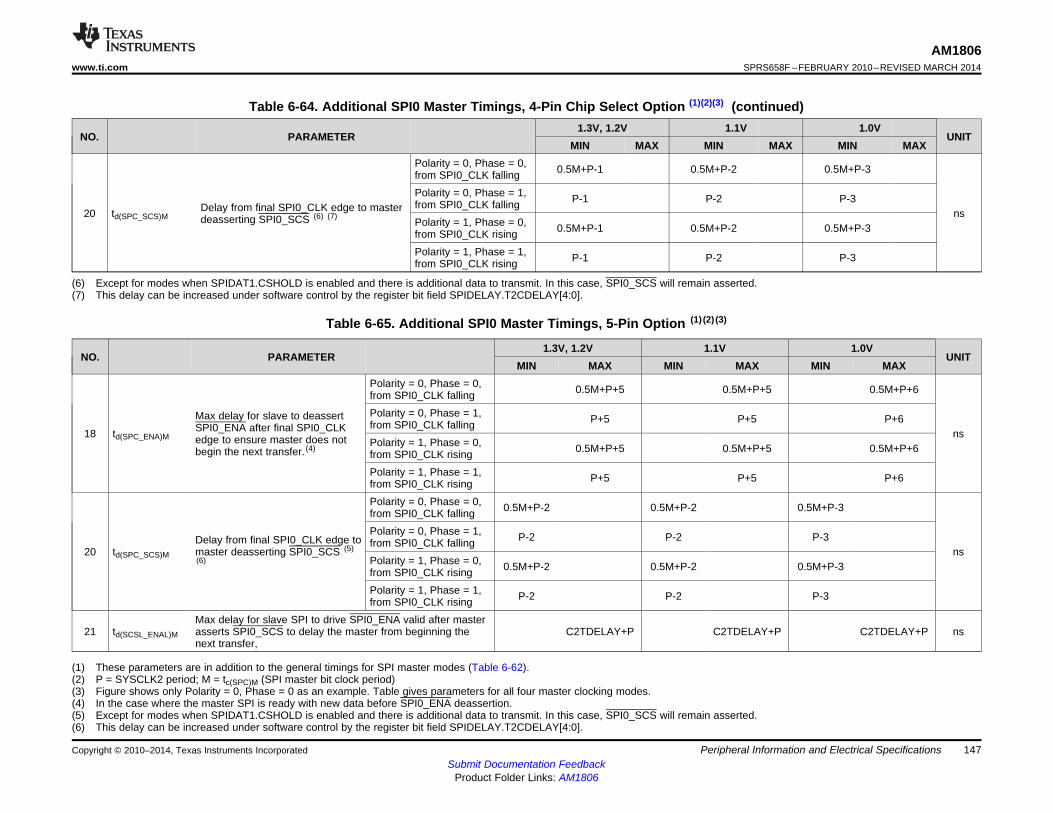
AM1806www.ti.com SPRS658F –FEBRUARY 2010–REVISED MARCH 2014
Table 6-64. Additional SPI0 Master Timings, 4-Pin Chip Select Option (1)(2)(3) (continued)1.3V, 1.2V 1.1V 1.0V
NO. PARAMETER UNITMIN MAX MIN MAX MIN MAX
Polarity = 0, Phase = 0, 0.5M+P-1 0.5M+P-2 0.5M+P-3from SPI0_CLK fallingPolarity = 0, Phase = 1, P-1 P-2 P-3from SPI0_CLK fallingDelay from final SPI0_CLK edge to master20 td(SPC_SCS)M nsdeasserting SPI0_SCS (6) (7) Polarity = 1, Phase = 0, 0.5M+P-1 0.5M+P-2 0.5M+P-3from SPI0_CLK risingPolarity = 1, Phase = 1, P-1 P-2 P-3from SPI0_CLK rising
(6) Except for modes when SPIDAT1.CSHOLD is enabled and there is additional data to transmit. In this case, SPI0_SCS will remain asserted.(7) This delay can be increased under software control by the register bit field SPIDELAY.T2CDELAY[4:0].
Table 6-65. Additional SPI0 Master Timings, 5-Pin Option (1) (2) (3)
1.3V, 1.2V 1.1V 1.0VNO. PARAMETER UNIT
MIN MAX MIN MAX MIN MAXPolarity = 0, Phase = 0, 0.5M+P+5 0.5M+P+5 0.5M+P+6from SPI0_CLK fallingPolarity = 0, Phase = 1,Max delay for slave to deassert P+5 P+5 P+6from SPI0_CLK fallingSPI0_ENA after final SPI0_CLK18 td(SPC_ENA)M nsedge to ensure master does not Polarity = 1, Phase = 0, 0.5M+P+5 0.5M+P+5 0.5M+P+6begin the next transfer. (4) from SPI0_CLK risingPolarity = 1, Phase = 1, P+5 P+5 P+6from SPI0_CLK risingPolarity = 0, Phase = 0, 0.5M+P-2 0.5M+P-2 0.5M+P-3from SPI0_CLK fallingPolarity = 0, Phase = 1, P-2 P-2 P-3Delay from final SPI0_CLK edge to from SPI0_CLK falling
20 td(SPC_SCS)M master deasserting SPI0_SCS (5) nsPolarity = 1, Phase = 0,(6) 0.5M+P-2 0.5M+P-2 0.5M+P-3from SPI0_CLK risingPolarity = 1, Phase = 1, P-2 P-2 P-3from SPI0_CLK rising
Max delay for slave SPI to drive SPI0_ENA valid after master21 td(SCSL_ENAL)M asserts SPI0_SCS to delay the master from beginning the C2TDELAY+P C2TDELAY+P C2TDELAY+P ns
next transfer,
(1) These parameters are in addition to the general timings for SPI master modes (Table 6-62).(2) P = SYSCLK2 period; M = tc(SPC)M (SPI master bit clock period)(3) Figure shows only Polarity = 0, Phase = 0 as an example. Table gives parameters for all four master clocking modes.(4) In the case where the master SPI is ready with new data before SPI0_ENA deassertion.(5) Except for modes when SPIDAT1.CSHOLD is enabled and there is additional data to transmit. In this case, SPI0_SCS will remain asserted.(6) This delay can be increased under software control by the register bit field SPIDELAY.T2CDELAY[4:0].
Copyright © 2010–2014, Texas Instruments Incorporated Peripheral Information and Electrical Specifications 147Submit Documentation Feedback
Product Folder Links: AM1806
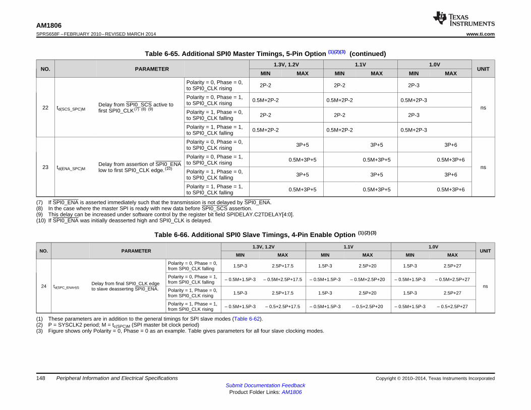
AM1806SPRS658F –FEBRUARY 2010–REVISED MARCH 2014 www.ti.com
Table 6-65. Additional SPI0 Master Timings, 5-Pin Option (1)(2)(3) (continued)1.3V, 1.2V 1.1V 1.0V
NO. PARAMETER UNITMIN MAX MIN MAX MIN MAX
Polarity = 0, Phase = 0, 2P-2 2P-2 2P-3to SPI0_CLK risingPolarity = 0, Phase = 1, 0.5M+2P-2 0.5M+2P-2 0.5M+2P-3to SPI0_CLK risingDelay from SPI0_SCS active to22 td(SCS_SPC)M nsfirst SPI0_CLK (7) (8) (9) Polarity = 1, Phase = 0, 2P-2 2P-2 2P-3to SPI0_CLK fallingPolarity = 1, Phase = 1, 0.5M+2P-2 0.5M+2P-2 0.5M+2P-3to SPI0_CLK fallingPolarity = 0, Phase = 0, 3P+5 3P+5 3P+6to SPI0_CLK risingPolarity = 0, Phase = 1, 0.5M+3P+5 0.5M+3P+5 0.5M+3P+6to SPI0_CLK risingDelay from assertion of SPI0_ENA23 td(ENA_SPC)M nslow to first SPI0_CLK edge. (10) Polarity = 1, Phase = 0, 3P+5 3P+5 3P+6to SPI0_CLK fallingPolarity = 1, Phase = 1, 0.5M+3P+5 0.5M+3P+5 0.5M+3P+6to SPI0_CLK falling
(7) If SPI0_ENA is asserted immediately such that the transmission is not delayed by SPI0_ENA.(8) In the case where the master SPI is ready with new data before SPI0_SCS assertion.(9) This delay can be increased under software control by the register bit field SPIDELAY.C2TDELAY[4:0].(10) If SPI0_ENA was initially deasserted high and SPI0_CLK is delayed.
Table 6-66. Additional SPI0 Slave Timings, 4-Pin Enable Option (1) (2) (3)
1.3V, 1.2V 1.1V 1.0VNO. PARAMETER UNIT
MIN MAX MIN MAX MIN MAX
Polarity = 0, Phase = 0, 1.5P-3 2.5P+17.5 1.5P-3 2.5P+20 1.5P-3 2.5P+27from SPI0_CLK falling
Polarity = 0, Phase = 1, – 0.5M+1.5P-3 – 0.5M+2.5P+17.5 – 0.5M+1.5P-3 – 0.5M+2.5P+20 – 0.5M+1.5P-3 – 0.5M+2.5P+27from SPI0_CLK fallingDelay from final SPI0_CLK edge24 td(SPC_ENAH)S nsto slave deasserting SPI0_ENA. Polarity = 1, Phase = 0, 1.5P-3 2.5P+17.5 1.5P-3 2.5P+20 1.5P-3 2.5P+27from SPI0_CLK rising
Polarity = 1, Phase = 1, – 0.5M+1.5P-3 – 0.5+2.5P+17.5 – 0.5M+1.5P-3 – 0.5+2.5P+20 – 0.5M+1.5P-3 – 0.5+2.5P+27from SPI0_CLK rising
(1) These parameters are in addition to the general timings for SPI slave modes (Table 6-62).(2) P = SYSCLK2 period; M = tc(SPC)M (SPI master bit clock period)(3) Figure shows only Polarity = 0, Phase = 0 as an example. Table gives parameters for all four slave clocking modes.
148 Peripheral Information and Electrical Specifications Copyright © 2010–2014, Texas Instruments IncorporatedSubmit Documentation Feedback
Product Folder Links: AM1806
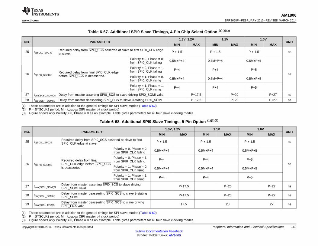
AM1806www.ti.com SPRS658F –FEBRUARY 2010–REVISED MARCH 2014
Table 6-67. Additional SPI0 Slave Timings, 4-Pin Chip Select Option (1) (2) (3)
1.3V, 1.2V 1.1V 1.0VNO. PARAMETER UNIT
MIN MAX MIN MAX MIN MAXRequired delay from SPI0_SCS asserted at slave to first SPI0_CLK edge25 td(SCSL_SPC)S P + 1.5 P + 1.5 P + 1.5 nsat slave.
Polarity = 0, Phase = 0, 0.5M+P+4 0.5M+P+4 0.5M+P+5from SPI0_CLK fallingPolarity = 0, Phase = 1, P+4 P+4 P+5from SPI0_CLK fallingRequired delay from final SPI0_CLK edge26 td(SPC_SCSH)S nsbefore SPI0_SCS is deasserted. Polarity = 1, Phase = 0, 0.5M+P+4 0.5M+P+4 0.5M+P+5from SPI0_CLK risingPolarity = 1, Phase = 1, P+4 P+4 P+5from SPI0_CLK rising
27 tena(SCSL_SOMI)S Delay from master asserting SPI0_SCS to slave driving SPI0_SOMI valid P+17.5 P+20 P+27 ns28 tdis(SCSH_SOMI)S Delay from master deasserting SPI0_SCS to slave 3-stating SPI0_SOMI P+17.5 P+20 P+27 ns
(1) These parameters are in addition to the general timings for SPI slave modes (Table 6-62).(2) P = SYSCLK2 period; M = tc(SPC)M (SPI master bit clock period)(3) Figure shows only Polarity = 0, Phase = 0 as an example. Table gives parameters for all four slave clocking modes.
Table 6-68. Additional SPI0 Slave Timings, 5-Pin Option (1) (2) (3)
1.3V, 1.2V 1.1V 1.0VNO. PARAMETER UNIT
MIN MAX MIN MAX MIN MAXRequired delay from SPI0_SCS asserted at slave to first25 td(SCSL_SPC)S P + 1.5 P + 1.5 P + 1.5 nsSPI0_CLK edge at slave.
Polarity = 0, Phase = 0, 0.5M+P+4 0.5M+P+4 0.5M+P+5from SPI0_CLK fallingPolarity = 0, Phase = 1, P+4 P+4 P+5Required delay from final from SPI0_CLK falling
26 td(SPC_SCSH)S SPI0_CLK edge before SPI0_SCS nsPolarity = 1, Phase = 0,is deasserted. 0.5M+P+4 0.5M+P+4 0.5M+P+5from SPI0_CLK risingPolarity = 1, Phase = 1, P+4 P+4 P+5from SPI0_CLK rising
Delay from master asserting SPI0_SCS to slave driving27 tena(SCSL_SOMI)S P+17.5 P+20 P+27 nsSPI0_SOMI validDelay from master deasserting SPI0_SCS to slave 3-stating28 tdis(SCSH_SOMI)S P+17.5 P+20 P+27 nsSPI0_SOMIDelay from master deasserting SPI0_SCS to slave driving29 tena(SCSL_ENA)S 17.5 20 27 nsSPI0_ENA valid
(1) These parameters are in addition to the general timings for SPI slave modes (Table 6-62).(2) P = SYSCLK2 period; M = tc(SPC)M (SPI master bit clock period)(3) Figure shows only Polarity = 0, Phase = 0 as an example. Table gives parameters for all four slave clocking modes.
Copyright © 2010–2014, Texas Instruments Incorporated Peripheral Information and Electrical Specifications 149Submit Documentation Feedback
Product Folder Links: AM1806
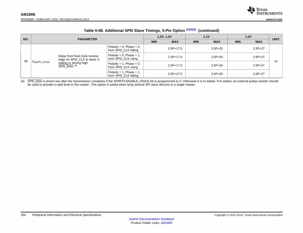
AM1806SPRS658F –FEBRUARY 2010–REVISED MARCH 2014 www.ti.com
Table 6-68. Additional SPI0 Slave Timings, 5-Pin Option (1)(2)(3) (continued)1.3V, 1.2V 1.1V 1.0V
NO. PARAMETER UNITMIN MAX MIN MAX MIN MAX
Polarity = 0, Phase = 0, 2.5P+17.5 2.5P+20 2.5P+27from SPI0_CLK fallingPolarity = 0, Phase = 1,Delay from final clock receive 2.5P+17.5 2.5P+20 2.5P+27from SPI0_CLK risingedge on SPI0_CLK to slave 3-30 tdis(SPC_ENA)S nsstating or driving high Polarity = 1, Phase = 0, 2.5P+17.5 2.5P+20 2.5P+27SPI0_ENA. (4) from SPI0_CLK risingPolarity = 1, Phase = 1, 2.5P+17.5 2.5P+20 2.5P+27from SPI0_CLK falling
(4) SPI0_ENA is driven low after the transmission completes if the SPIINT0.ENABLE_HIGHZ bit is programmed to 0. Otherwise it is tri-stated. If tri-stated, an external pullup resistor shouldbe used to provide a valid level to the master. This option is useful when tying several SPI slave devices to a single master.
150 Peripheral Information and Electrical Specifications Copyright © 2010–2014, Texas Instruments IncorporatedSubmit Documentation Feedback
Product Folder Links: AM1806
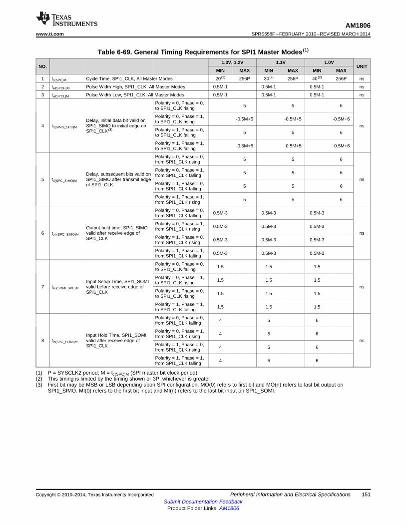
AM1806www.ti.com SPRS658F –FEBRUARY 2010–REVISED MARCH 2014
Table 6-69. General Timing Requirements for SPI1 Master Modes (1)
1.3V, 1.2V 1.1V 1.0VNO. UNIT
MIN MAX MIN MAX MIN MAX
1 tc(SPC)M Cycle Time, SPI1_CLK, All Master Modes 20 (2) 256P 30 (2) 256P 40 (2) 256P ns
2 tw(SPCH)M Pulse Width High, SPI1_CLK, All Master Modes 0.5M-1 0.5M-1 0.5M-1 ns
3 tw(SPCL)M Pulse Width Low, SPI1_CLK, All Master Modes 0.5M-1 0.5M-1 0.5M-1 ns
Polarity = 0, Phase = 0, 5 5 6to SPI1_CLK rising
Polarity = 0, Phase = 1, -0.5M+5 -0.5M+5 -0.5M+6Delay, initial data bit valid on to SPI1_CLK rising4 td(SIMO_SPC)M SPI1_SIMO to initial edge on ns
Polarity = 1, Phase = 0,SPI1_CLK (3)5 5 6to SPI1_CLK falling
Polarity = 1, Phase = 1, -0.5M+5 -0.5M+5 -0.5M+6to SPI1_CLK falling
Polarity = 0, Phase = 0, 5 5 6from SPI1_CLK rising
Polarity = 0, Phase = 1, 5 5 6Delay, subsequent bits valid on from SPI1_CLK falling5 td(SPC_SIMO)M SPI1_SIMO after transmit edge ns
Polarity = 1, Phase = 0,of SPI1_CLK 5 5 6from SPI1_CLK falling
Polarity = 1, Phase = 1, 5 5 6from SPI1_CLK rising
Polarity = 0, Phase = 0, 0.5M-3 0.5M-3 0.5M-3from SPI1_CLK falling
Polarity = 0, Phase = 1, 0.5M-3 0.5M-3 0.5M-3Output hold time, SPI1_SIMO from SPI1_CLK rising6 toh(SPC_SIMO)M valid after receive edge of ns
Polarity = 1, Phase = 0,SPI1_CLK 0.5M-3 0.5M-3 0.5M-3from SPI1_CLK rising
Polarity = 1, Phase = 1, 0.5M-3 0.5M-3 0.5M-3from SPI1_CLK falling
Polarity = 0, Phase = 0, 1.5 1.5 1.5to SPI1_CLK falling
Polarity = 0, Phase = 1, 1.5 1.5 1.5Input Setup Time, SPI1_SOMI to SPI1_CLK rising7 tsu(SOMI_SPC)M valid before receive edge of ns
Polarity = 1, Phase = 0,SPI1_CLK 1.5 1.5 1.5to SPI1_CLK rising
Polarity = 1, Phase = 1, 1.5 1.5 1.5to SPI1_CLK falling
Polarity = 0, Phase = 0, 4 5 6from SPI1_CLK falling
Polarity = 0, Phase = 1, 4 5 6Input Hold Time, SPI1_SOMI from SPI1_CLK rising8 tih(SPC_SOMI)M valid after receive edge of ns
Polarity = 1, Phase = 0,SPI1_CLK 4 5 6from SPI1_CLK rising
Polarity = 1, Phase = 1, 4 5 6from SPI1_CLK falling
(1) P = SYSCLK2 period; M = tc(SPC)M (SPI master bit clock period)(2) This timing is limited by the timing shown or 3P, whichever is greater.(3) First bit may be MSB or LSB depending upon SPI configuration. MO(0) refers to first bit and MO(n) refers to last bit output on
SPI1_SIMO. MI(0) refers to the first bit input and MI(n) refers to the last bit input on SPI1_SOMI.
Copyright © 2010–2014, Texas Instruments Incorporated Peripheral Information and Electrical Specifications 151Submit Documentation Feedback
Product Folder Links: AM1806
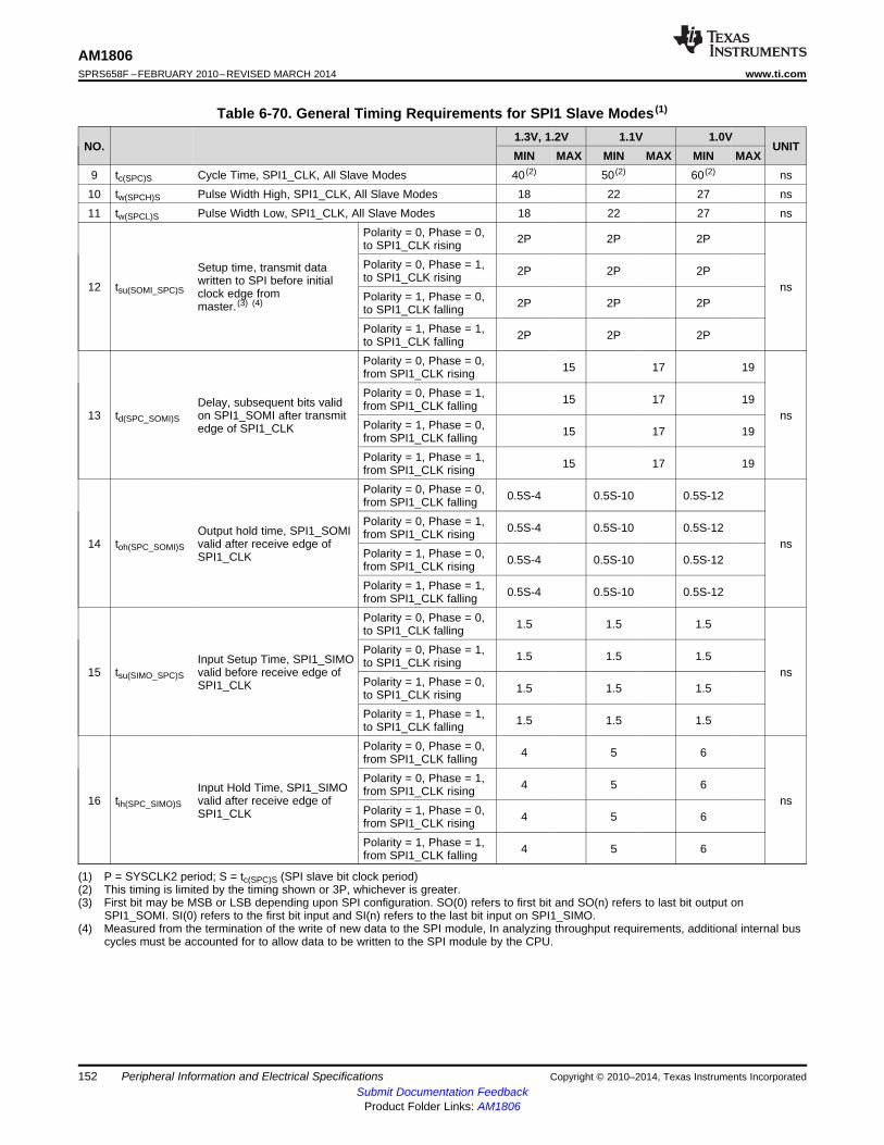
AM1806SPRS658F –FEBRUARY 2010–REVISED MARCH 2014 www.ti.com
Table 6-70. General Timing Requirements for SPI1 Slave Modes (1)
1.3V, 1.2V 1.1V 1.0VNO. UNIT
MIN MAX MIN MAX MIN MAX9 tc(SPC)S Cycle Time, SPI1_CLK, All Slave Modes 40 (2) 50 (2) 60 (2) ns10 tw(SPCH)S Pulse Width High, SPI1_CLK, All Slave Modes 18 22 27 ns11 tw(SPCL)S Pulse Width Low, SPI1_CLK, All Slave Modes 18 22 27 ns
Polarity = 0, Phase = 0, 2P 2P 2Pto SPI1_CLK risingPolarity = 0, Phase = 1,Setup time, transmit data 2P 2P 2Pto SPI1_CLK risingwritten to SPI before initial12 tsu(SOMI_SPC)S nsclock edge from Polarity = 1, Phase = 0, 2P 2P 2Pmaster. (3) (4) to SPI1_CLK fallingPolarity = 1, Phase = 1, 2P 2P 2Pto SPI1_CLK fallingPolarity = 0, Phase = 0, 15 17 19from SPI1_CLK risingPolarity = 0, Phase = 1, 15 17 19Delay, subsequent bits valid from SPI1_CLK falling
13 td(SPC_SOMI)S on SPI1_SOMI after transmit nsPolarity = 1, Phase = 0,edge of SPI1_CLK 15 17 19from SPI1_CLK fallingPolarity = 1, Phase = 1, 15 17 19from SPI1_CLK risingPolarity = 0, Phase = 0, 0.5S-4 0.5S-10 0.5S-12from SPI1_CLK fallingPolarity = 0, Phase = 1, 0.5S-4 0.5S-10 0.5S-12Output hold time, SPI1_SOMI from SPI1_CLK rising
14 toh(SPC_SOMI)S valid after receive edge of nsPolarity = 1, Phase = 0,SPI1_CLK 0.5S-4 0.5S-10 0.5S-12from SPI1_CLK risingPolarity = 1, Phase = 1, 0.5S-4 0.5S-10 0.5S-12from SPI1_CLK fallingPolarity = 0, Phase = 0, 1.5 1.5 1.5to SPI1_CLK fallingPolarity = 0, Phase = 1, 1.5 1.5 1.5Input Setup Time, SPI1_SIMO to SPI1_CLK rising
15 tsu(SIMO_SPC)S valid before receive edge of nsPolarity = 1, Phase = 0,SPI1_CLK 1.5 1.5 1.5to SPI1_CLK risingPolarity = 1, Phase = 1, 1.5 1.5 1.5to SPI1_CLK fallingPolarity = 0, Phase = 0, 4 5 6from SPI1_CLK fallingPolarity = 0, Phase = 1, 4 5 6Input Hold Time, SPI1_SIMO from SPI1_CLK rising
16 tih(SPC_SIMO)S valid after receive edge of nsPolarity = 1, Phase = 0,SPI1_CLK 4 5 6from SPI1_CLK risingPolarity = 1, Phase = 1, 4 5 6from SPI1_CLK falling
(1) P = SYSCLK2 period; S = tc(SPC)S (SPI slave bit clock period)(2) This timing is limited by the timing shown or 3P, whichever is greater.(3) First bit may be MSB or LSB depending upon SPI configuration. SO(0) refers to first bit and SO(n) refers to last bit output on
SPI1_SOMI. SI(0) refers to the first bit input and SI(n) refers to the last bit input on SPI1_SIMO.(4) Measured from the termination of the write of new data to the SPI module, In analyzing throughput requirements, additional internal bus
cycles must be accounted for to allow data to be written to the SPI module by the CPU.
152 Peripheral Information and Electrical Specifications Copyright © 2010–2014, Texas Instruments IncorporatedSubmit Documentation Feedback
Product Folder Links: AM1806
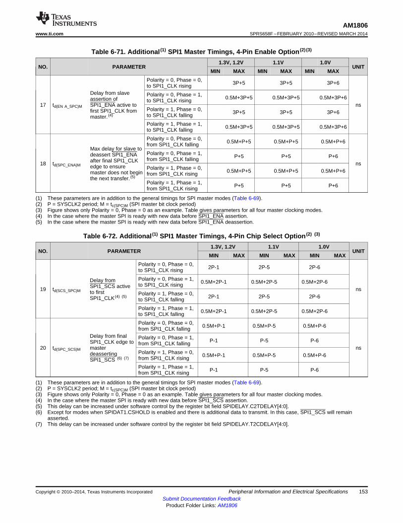
AM1806www.ti.com SPRS658F –FEBRUARY 2010–REVISED MARCH 2014
Table 6-71. Additional (1) SPI1 Master Timings, 4-Pin Enable Option (2) (3)
1.3V, 1.2V 1.1V 1.0VNO. PARAMETER UNIT
MIN MAX MIN MAX MIN MAXPolarity = 0, Phase = 0, 3P+5 3P+5 3P+6to SPI1_CLK rising
Delay from slave Polarity = 0, Phase = 1, 0.5M+3P+5 0.5M+3P+5 0.5M+3P+6assertion of to SPI1_CLK rising17 td(EN A_SPC)M SPI1_ENA active to ns
Polarity = 1, Phase = 0,first SPI1_CLK from 3P+5 3P+5 3P+6to SPI1_CLK fallingmaster. (4)
Polarity = 1, Phase = 1, 0.5M+3P+5 0.5M+3P+5 0.5M+3P+6to SPI1_CLK fallingPolarity = 0, Phase = 0, 0.5M+P+5 0.5M+P+5 0.5M+P+6from SPI1_CLK falling
Max delay for slave toPolarity = 0, Phase = 1,deassert SPI1_ENA P+5 P+5 P+6from SPI1_CLK fallingafter final SPI1_CLK18 td(SPC_ENA)M nsedge to ensure Polarity = 1, Phase = 0, 0.5M+P+5 0.5M+P+5 0.5M+P+6master does not begin from SPI1_CLK rising
the next transfer. (5)Polarity = 1, Phase = 1, P+5 P+5 P+6from SPI1_CLK rising
(1) These parameters are in addition to the general timings for SPI master modes (Table 6-69).(2) P = SYSCLK2 period; M = tc(SPC)M (SPI master bit clock period)(3) Figure shows only Polarity = 0, Phase = 0 as an example. Table gives parameters for all four master clocking modes.(4) In the case where the master SPI is ready with new data before SPI1_ENA assertion.(5) In the case where the master SPI is ready with new data before SPI1_ENA deassertion.
Table 6-72. Additional (1) SPI1 Master Timings, 4-Pin Chip Select Option (2) (3)
1.3V, 1.2V 1.1V 1.0VNO. PARAMETER UNIT
MIN MAX MIN MAX MIN MAXPolarity = 0, Phase = 0, 2P-1 2P-5 2P-6to SPI1_CLK risingPolarity = 0, Phase = 1,Delay from 0.5M+2P-1 0.5M+2P-5 0.5M+2P-6to SPI1_CLK risingSPI1_SCS active19 td(SCS_SPC)M nsto first Polarity = 1, Phase = 0, 2P-1 2P-5 2P-6SPI1_CLK (4) (5) to SPI1_CLK fallingPolarity = 1, Phase = 1, 0.5M+2P-1 0.5M+2P-5 0.5M+2P-6to SPI1_CLK fallingPolarity = 0, Phase = 0, 0.5M+P-1 0.5M+P-5 0.5M+P-6from SPI1_CLK falling
Delay from final Polarity = 0, Phase = 1, P-1 P-5 P-6SPI1_CLK edge to from SPI1_CLK falling20 td(SPC_SCS)M master ns
Polarity = 1, Phase = 0,deasserting 0.5M+P-1 0.5M+P-5 0.5M+P-6from SPI1_CLK risingSPI1_SCS (6) (7)
Polarity = 1, Phase = 1, P-1 P-5 P-6from SPI1_CLK rising
(1) These parameters are in addition to the general timings for SPI master modes (Table 6-69).(2) P = SYSCLK2 period; M = tc(SPC)M (SPI master bit clock period)(3) Figure shows only Polarity = 0, Phase = 0 as an example. Table gives parameters for all four master clocking modes.(4) In the case where the master SPI is ready with new data before SPI1_SCS assertion.(5) This delay can be increased under software control by the register bit field SPIDELAY.C2TDELAY[4:0].(6) Except for modes when SPIDAT1.CSHOLD is enabled and there is additional data to transmit. In this case, SPI1_SCS will remain
asserted.(7) This delay can be increased under software control by the register bit field SPIDELAY.T2CDELAY[4:0].
Copyright © 2010–2014, Texas Instruments Incorporated Peripheral Information and Electrical Specifications 153Submit Documentation Feedback
Product Folder Links: AM1806
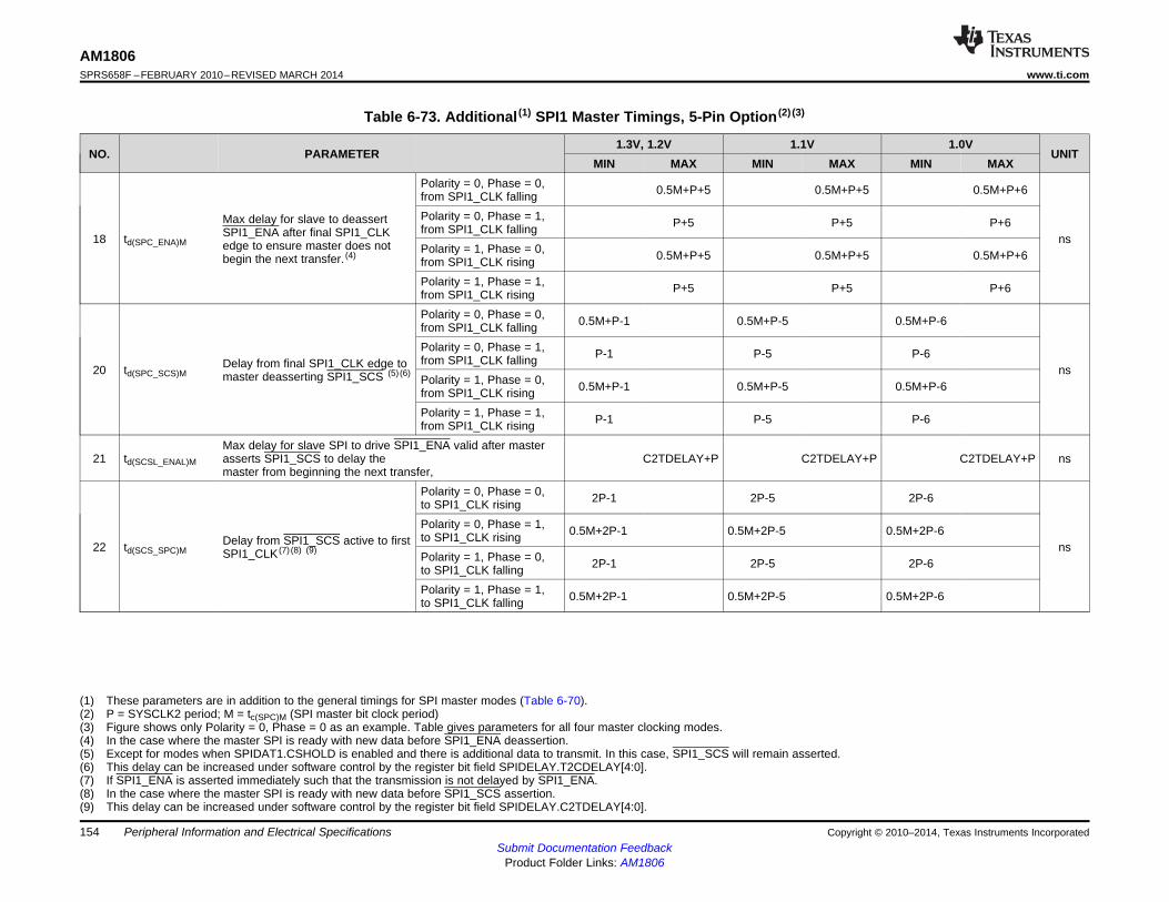
AM1806SPRS658F –FEBRUARY 2010–REVISED MARCH 2014 www.ti.com
Table 6-73. Additional (1) SPI1 Master Timings, 5-Pin Option (2) (3)
1.3V, 1.2V 1.1V 1.0VNO. PARAMETER UNIT
MIN MAX MIN MAX MIN MAXPolarity = 0, Phase = 0, 0.5M+P+5 0.5M+P+5 0.5M+P+6from SPI1_CLK fallingPolarity = 0, Phase = 1,Max delay for slave to deassert P+5 P+5 P+6from SPI1_CLK fallingSPI1_ENA after final SPI1_CLK18 td(SPC_ENA)M nsedge to ensure master does not Polarity = 1, Phase = 0, 0.5M+P+5 0.5M+P+5 0.5M+P+6begin the next transfer. (4) from SPI1_CLK risingPolarity = 1, Phase = 1, P+5 P+5 P+6from SPI1_CLK risingPolarity = 0, Phase = 0, 0.5M+P-1 0.5M+P-5 0.5M+P-6from SPI1_CLK fallingPolarity = 0, Phase = 1, P-1 P-5 P-6from SPI1_CLK fallingDelay from final SPI1_CLK edge to20 td(SPC_SCS)M nsmaster deasserting SPI1_SCS (5) (6) Polarity = 1, Phase = 0, 0.5M+P-1 0.5M+P-5 0.5M+P-6from SPI1_CLK risingPolarity = 1, Phase = 1, P-1 P-5 P-6from SPI1_CLK rising
Max delay for slave SPI to drive SPI1_ENA valid after master21 td(SCSL_ENAL)M asserts SPI1_SCS to delay the C2TDELAY+P C2TDELAY+P C2TDELAY+P ns
master from beginning the next transfer,Polarity = 0, Phase = 0, 2P-1 2P-5 2P-6to SPI1_CLK risingPolarity = 0, Phase = 1, 0.5M+2P-1 0.5M+2P-5 0.5M+2P-6to SPI1_CLK risingDelay from SPI1_SCS active to first22 td(SCS_SPC)M nsSPI1_CLK (7) (8) (9) Polarity = 1, Phase = 0, 2P-1 2P-5 2P-6to SPI1_CLK fallingPolarity = 1, Phase = 1, 0.5M+2P-1 0.5M+2P-5 0.5M+2P-6to SPI1_CLK falling
(1) These parameters are in addition to the general timings for SPI master modes (Table 6-70).(2) P = SYSCLK2 period; M = tc(SPC)M (SPI master bit clock period)(3) Figure shows only Polarity = 0, Phase = 0 as an example. Table gives parameters for all four master clocking modes.(4) In the case where the master SPI is ready with new data before SPI1_ENA deassertion.(5) Except for modes when SPIDAT1.CSHOLD is enabled and there is additional data to transmit. In this case, SPI1_SCS will remain asserted.(6) This delay can be increased under software control by the register bit field SPIDELAY.T2CDELAY[4:0].(7) If SPI1_ENA is asserted immediately such that the transmission is not delayed by SPI1_ENA.(8) In the case where the master SPI is ready with new data before SPI1_SCS assertion.(9) This delay can be increased under software control by the register bit field SPIDELAY.C2TDELAY[4:0].
154 Peripheral Information and Electrical Specifications Copyright © 2010–2014, Texas Instruments IncorporatedSubmit Documentation Feedback
Product Folder Links: AM1806
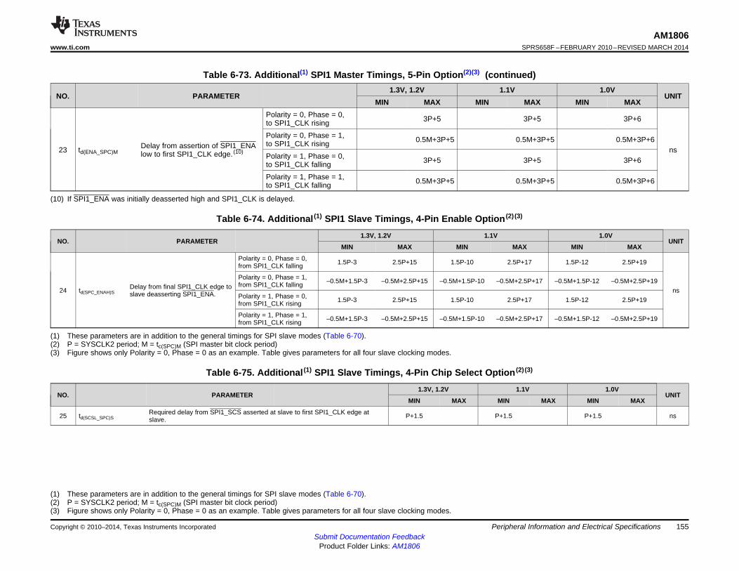
AM1806www.ti.com SPRS658F –FEBRUARY 2010–REVISED MARCH 2014
Table 6-73. Additional(1) SPI1 Master Timings, 5-Pin Option(2)(3) (continued)1.3V, 1.2V 1.1V 1.0V
NO. PARAMETER UNITMIN MAX MIN MAX MIN MAX
Polarity = 0, Phase = 0, 3P+5 3P+5 3P+6to SPI1_CLK risingPolarity = 0, Phase = 1, 0.5M+3P+5 0.5M+3P+5 0.5M+3P+6to SPI1_CLK risingDelay from assertion of SPI1_ENA23 td(ENA_SPC)M nslow to first SPI1_CLK edge. (10) Polarity = 1, Phase = 0, 3P+5 3P+5 3P+6to SPI1_CLK fallingPolarity = 1, Phase = 1, 0.5M+3P+5 0.5M+3P+5 0.5M+3P+6to SPI1_CLK falling
(10) If SPI1_ENA was initially deasserted high and SPI1_CLK is delayed.
Table 6-74. Additional (1) SPI1 Slave Timings, 4-Pin Enable Option (2) (3)
1.3V, 1.2V 1.1V 1.0VNO. PARAMETER UNIT
MIN MAX MIN MAX MIN MAX
Polarity = 0, Phase = 0, 1.5P-3 2.5P+15 1.5P-10 2.5P+17 1.5P-12 2.5P+19from SPI1_CLK falling
Polarity = 0, Phase = 1, –0.5M+1.5P-3 –0.5M+2.5P+15 –0.5M+1.5P-10 –0.5M+2.5P+17 –0.5M+1.5P-12 –0.5M+2.5P+19from SPI1_CLK fallingDelay from final SPI1_CLK edge to24 td(SPC_ENAH)S nsslave deasserting SPI1_ENA. Polarity = 1, Phase = 0, 1.5P-3 2.5P+15 1.5P-10 2.5P+17 1.5P-12 2.5P+19from SPI1_CLK rising
Polarity = 1, Phase = 1, –0.5M+1.5P-3 –0.5M+2.5P+15 –0.5M+1.5P-10 –0.5M+2.5P+17 –0.5M+1.5P-12 –0.5M+2.5P+19from SPI1_CLK rising
(1) These parameters are in addition to the general timings for SPI slave modes (Table 6-70).(2) P = SYSCLK2 period; M = tc(SPC)M (SPI master bit clock period)(3) Figure shows only Polarity = 0, Phase = 0 as an example. Table gives parameters for all four slave clocking modes.
Table 6-75. Additional (1) SPI1 Slave Timings, 4-Pin Chip Select Option (2) (3)
1.3V, 1.2V 1.1V 1.0VNO. PARAMETER UNIT
MIN MAX MIN MAX MIN MAX
Required delay from SPI1_SCS asserted at slave to first SPI1_CLK edge at25 td(SCSL_SPC)S P+1.5 P+1.5 P+1.5 nsslave.
(1) These parameters are in addition to the general timings for SPI slave modes (Table 6-70).(2) P = SYSCLK2 period; M = tc(SPC)M (SPI master bit clock period)(3) Figure shows only Polarity = 0, Phase = 0 as an example. Table gives parameters for all four slave clocking modes.
Copyright © 2010–2014, Texas Instruments Incorporated Peripheral Information and Electrical Specifications 155Submit Documentation Feedback
Product Folder Links: AM1806
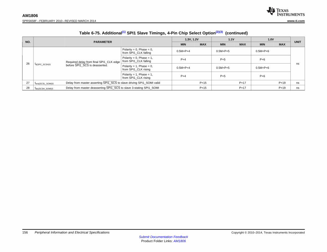
AM1806SPRS658F –FEBRUARY 2010–REVISED MARCH 2014 www.ti.com
Table 6-75. Additional(1) SPI1 Slave Timings, 4-Pin Chip Select Option(2)(3) (continued)1.3V, 1.2V 1.1V 1.0V
NO. PARAMETER UNITMIN MAX MIN MAX MIN MAX
Polarity = 0, Phase = 0, 0.5M+P+4 0.5M+P+5 0.5M+P+6from SPI1_CLK falling
Polarity = 0, Phase = 1, P+4 P+5 P+6from SPI1_CLK fallingRequired delay from final SPI1_CLK edge26 td(SPC_SCSH)S nsbefore SPI1_SCS is deasserted. Polarity = 1, Phase = 0, 0.5M+P+4 0.5M+P+5 0.5M+P+6from SPI1_CLK rising
Polarity = 1, Phase = 1, P+4 P+5 P+6from SPI1_CLK rising
27 tena(SCSL_SOMI)S Delay from master asserting SPI1_SCS to slave driving SPI1_SOMI valid P+15 P+17 P+19 ns
28 tdis(SCSH_SOMI)S Delay from master deasserting SPI1_SCS to slave 3-stating SPI1_SOMI P+15 P+17 P+19 ns
156 Peripheral Information and Electrical Specifications Copyright © 2010–2014, Texas Instruments IncorporatedSubmit Documentation Feedback
Product Folder Links: AM1806
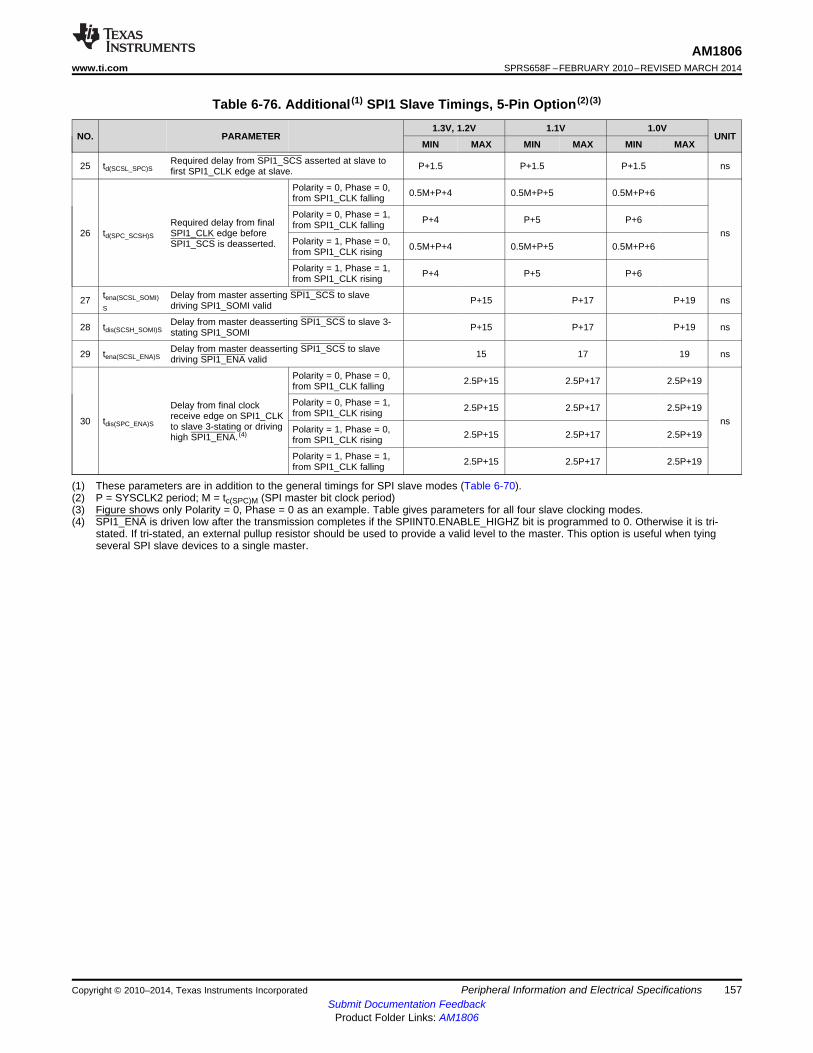
AM1806www.ti.com SPRS658F –FEBRUARY 2010–REVISED MARCH 2014
Table 6-76. Additional (1) SPI1 Slave Timings, 5-Pin Option (2) (3)
1.3V, 1.2V 1.1V 1.0VNO. PARAMETER UNIT
MIN MAX MIN MAX MIN MAX
Required delay from SPI1_SCS asserted at slave to25 td(SCSL_SPC)S P+1.5 P+1.5 P+1.5 nsfirst SPI1_CLK edge at slave.
Polarity = 0, Phase = 0, 0.5M+P+4 0.5M+P+5 0.5M+P+6from SPI1_CLK falling
Polarity = 0, Phase = 1, P+4 P+5 P+6Required delay from final from SPI1_CLK falling26 td(SPC_SCSH)S SPI1_CLK edge before ns
Polarity = 1, Phase = 0,SPI1_SCS is deasserted. 0.5M+P+4 0.5M+P+5 0.5M+P+6from SPI1_CLK rising
Polarity = 1, Phase = 1, P+4 P+5 P+6from SPI1_CLK rising
tena(SCSL_SOMI) Delay from master asserting SPI1_SCS to slave27 P+15 P+17 P+19 nsS driving SPI1_SOMI valid
Delay from master deasserting SPI1_SCS to slave 3-28 tdis(SCSH_SOMI)S P+15 P+17 P+19 nsstating SPI1_SOMI
Delay from master deasserting SPI1_SCS to slave29 tena(SCSL_ENA)S 15 17 19 nsdriving SPI1_ENA valid
Polarity = 0, Phase = 0, 2.5P+15 2.5P+17 2.5P+19from SPI1_CLK falling
Polarity = 0, Phase = 1,Delay from final clock 2.5P+15 2.5P+17 2.5P+19from SPI1_CLK risingreceive edge on SPI1_CLK30 tdis(SPC_ENA)S nsto slave 3-stating or driving Polarity = 1, Phase = 0, 2.5P+15 2.5P+17 2.5P+19high SPI1_ENA. (4)from SPI1_CLK rising
Polarity = 1, Phase = 1, 2.5P+15 2.5P+17 2.5P+19from SPI1_CLK falling
(1) These parameters are in addition to the general timings for SPI slave modes (Table 6-70).(2) P = SYSCLK2 period; M = tc(SPC)M (SPI master bit clock period)(3) Figure shows only Polarity = 0, Phase = 0 as an example. Table gives parameters for all four slave clocking modes.(4) SPI1_ENA is driven low after the transmission completes if the SPIINT0.ENABLE_HIGHZ bit is programmed to 0. Otherwise it is tri-
stated. If tri-stated, an external pullup resistor should be used to provide a valid level to the master. This option is useful when tyingseveral SPI slave devices to a single master.
Copyright © 2010–2014, Texas Instruments Incorporated Peripheral Information and Electrical Specifications 157Submit Documentation Feedback
Product Folder Links: AM1806
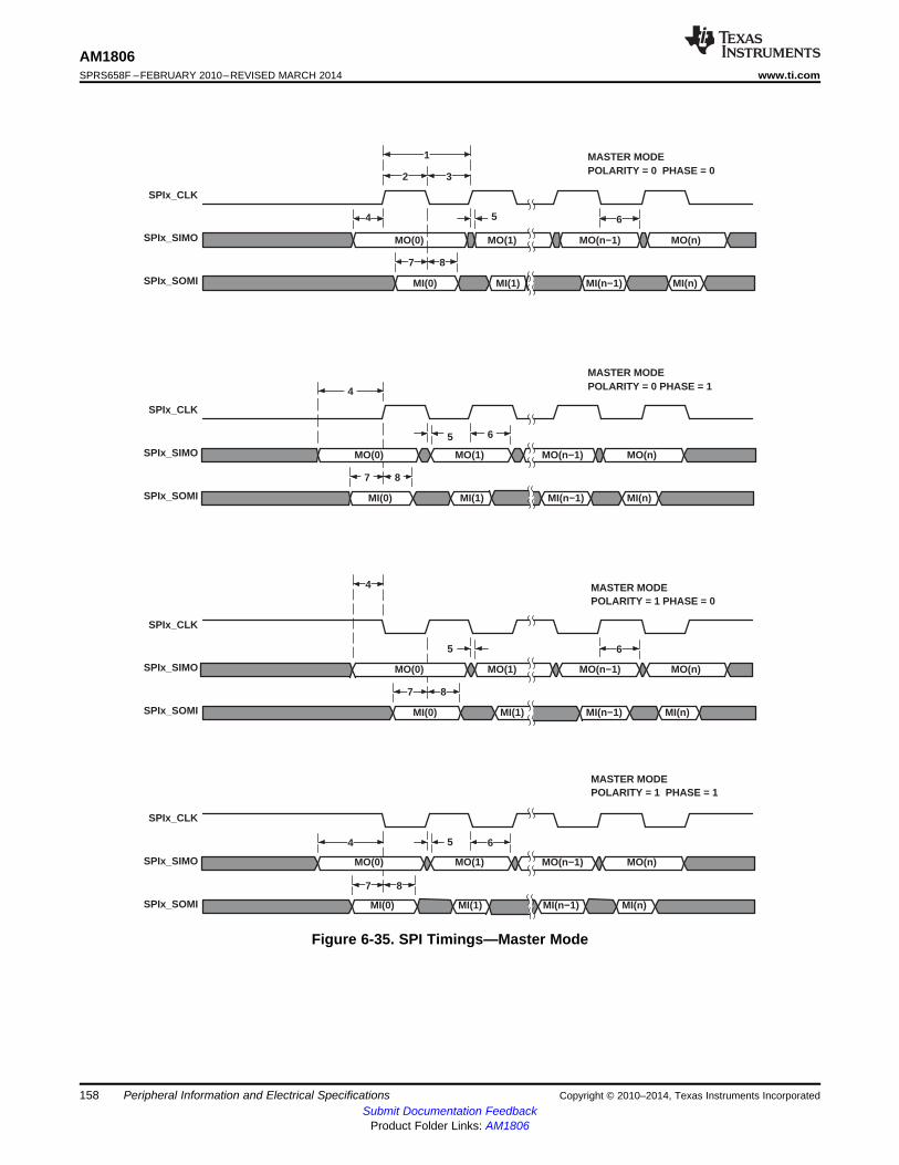
SPIx_CLK
SPIx_SIMO
SPIx_SOMI
SPIx_CLK
SPIx_SIMO
SPIx_SOMI
SPIx_CLK
SPIx_SIMO
SPIx_SOMI
SPIx_CLK
SPIx_SIMO
SPIx_SOMI
MO(0) MO(1) MO(n−1) MO(n)
MI(0) MI(1) MI(n−1) MI(n)
MO(0) MO(1) MO(n−1) MO(n)
MI(0) MI(1) MI(n−1) MI(n)
MO(0) MO(1) MO(n−1) MO(n)
MI(0) MI(1) MI(n−1) MI(n)
MO(0) MO(1) MO(n−1) MO(n)
MI(0) MI(1) MI(n−1) MI(n)
6
6
7
7
7
7
8
8
8
8
32
6
1
4
4
4
4 5
5
5 6
MASTER MODEPOLARITY = 0 PHASE = 0
MASTER MODEPOLARITY = 0 PHASE = 1
MASTER MODEPOLARITY = 1 PHASE = 0
MASTER MODEPOLARITY = 1 PHASE = 1
5
AM1806SPRS658F –FEBRUARY 2010–REVISED MARCH 2014 www.ti.com
Figure 6-35. SPI Timings—Master Mode
158 Peripheral Information and Electrical Specifications Copyright © 2010–2014, Texas Instruments IncorporatedSubmit Documentation Feedback
Product Folder Links: AM1806
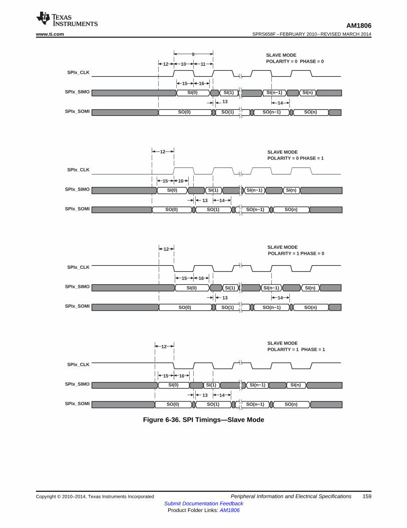
SPIx_CLK
SPIx_SIMO
SPIx_SOMI
SPIx_CLK
SPIx_SIMO
SPIx_SOMI
SPIx_CLK
SPIx_SIMO
SPIx_SOMI
SPIx_CLK
SPIx_SIMO
SPIx_SOMI
SI(0) SI(1) SI(n−1) SI(n)
SO(0) SO(1) SO(n−1) SO(n)
SI(0) SI(1) SI(n−1) SI(n)
SO(0) SO(1) SO(n−1) SO(n)
SI(0) SI(1) SI(n−1) SI(n)
SO(0) SO(1) SO(n−1) SO(n)
SI(0) SI(1) SI(n−1) SI(n)
SO(0) SO(1) SO(n−1) SO(n)
14
14
15
15
15
15
16
16
16
16
1110
14
9
12
12
12
12
13
13
13
13
14
SLAVE MODEPOLARITY = 0 PHASE = 0
SLAVE MODEPOLARITY = 0 PHASE = 1
SLAVE MODEPOLARITY = 1 PHASE = 0
SLAVE MODEPOLARITY = 1 PHASE = 1
AM1806www.ti.com SPRS658F –FEBRUARY 2010–REVISED MARCH 2014
Figure 6-36. SPI Timings—Slave Mode
Copyright © 2010–2014, Texas Instruments Incorporated Peripheral Information and Electrical Specifications 159Submit Documentation Feedback
Product Folder Links: AM1806
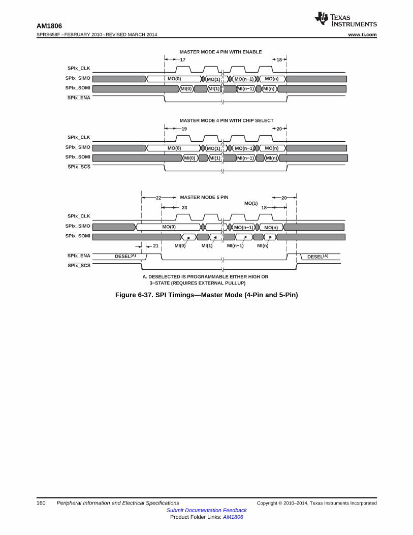
MASTER MODE 4 PIN WITH CHIP SELECT
SPIx_CLK
SPIx_SIMO
SPIx_SOMI
SPIx_ENA
SPIx_CLK
SPIx_SIMO
SPIx_SOMI
SPIx_SCS
SPIx_CLK
SPIx_SIMO
SPIx_SOMI
SPIx_ENA
SPIx_SCS
MO(0) MO(1) MO(n−1) MO(n)
MI(0) MI(1) MI(n−1) MI(n)
MO(0) MO(1) MO(n−1) MO(n)
MI(0) MI(1) MI(n−1) MI(n)
MO(0)
MO(1)
MO(n−1) MO(n)
MI(0) MI(1) MI(n−1) MI(n)
17
19
21
22
23
20
18
20
18
MASTER MODE 4 PIN WITH ENABLE
MASTER MODE 5 PIN
A. DESELECTED IS PROGRAMMABLE EITHER HIGH OR 3−STATE (REQUIRES EXTERNAL PULLUP)
DESEL(A) DESEL(A)
AM1806SPRS658F –FEBRUARY 2010–REVISED MARCH 2014 www.ti.com
Figure 6-37. SPI Timings—Master Mode (4-Pin and 5-Pin)
160 Peripheral Information and Electrical Specifications Copyright © 2010–2014, Texas Instruments IncorporatedSubmit Documentation Feedback
Product Folder Links: AM1806
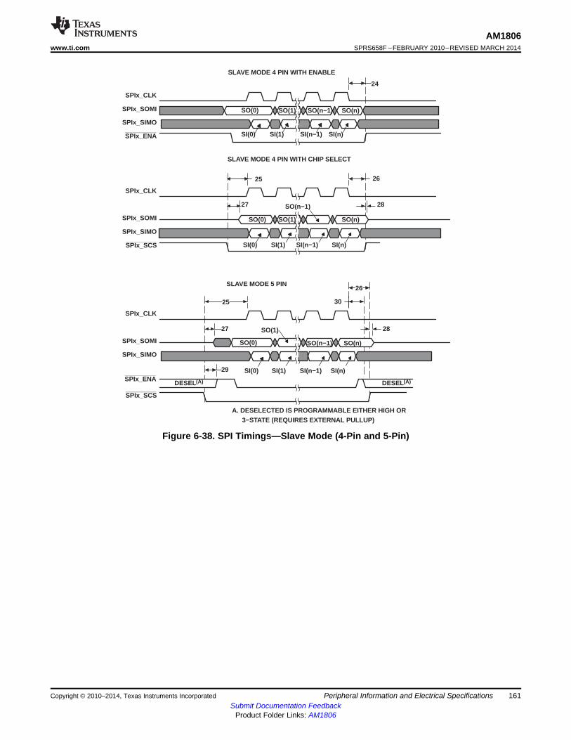
27
SPIx_CLK
SPIx_SOMI
SPIx_SIMO
SPIx_ENA
SPIx_CLK
SPIx_SOMI
SPIx_SIMO
SPIx_SCS
SPIx_CLK
SPIx_SOMI
SPIx_SIMO
SPIx_ENA
SPIx_SCS
SO(0) SO(1) SO(n−1) SO(n)
SI(0) SI(1) SI(n−1) SI(n)
SO(0) SO(1)
SO(n−1)
SO(n)
SI(0) SI(1) SI(n−1) SI(n)
SO(0)
SO(1)
SO(n−1) SO(n)
SI(0) SI(1) SI(n−1) SI(n)
24
26
28
26
30
28
25
25
27
29
SLAVE MODE 4 PIN WITH ENABLE
SLAVE MODE 4 PIN WITH CHIP SELECT
SLAVE MODE 5 PIN
DESEL(A) DESEL(A)
A. DESELECTED IS PROGRAMMABLE EITHER HIGH OR 3−STATE (REQUIRES EXTERNAL PULLUP)
AM1806www.ti.com SPRS658F –FEBRUARY 2010–REVISED MARCH 2014
Figure 6-38. SPI Timings—Slave Mode (4-Pin and 5-Pin)
Copyright © 2010–2014, Texas Instruments Incorporated Peripheral Information and Electrical Specifications 161Submit Documentation Feedback
Product Folder Links: AM1806
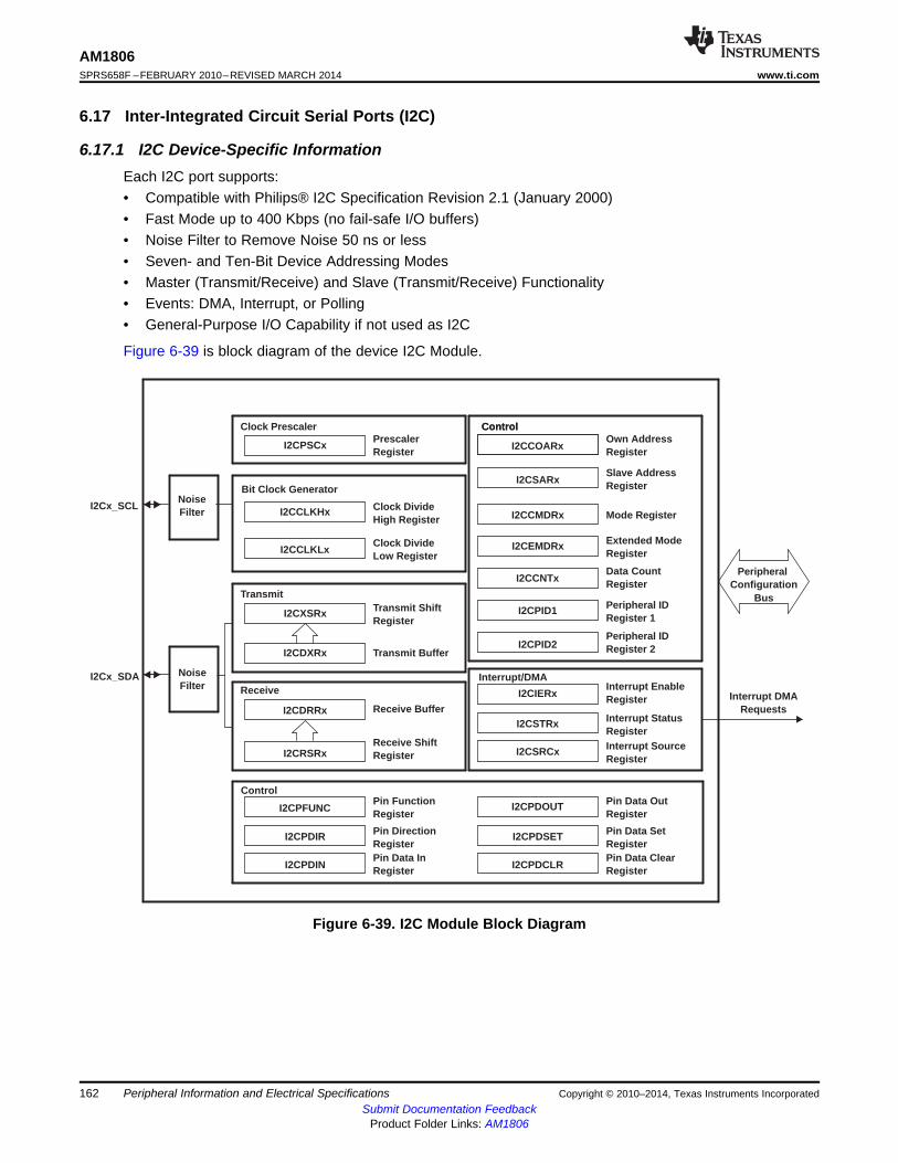
Peripheral Configuration
Bus
NoiseFilter
NoiseFilter
Clock Prescaler
I2CPSCxPrescalerRegister
Bit Clock Generator
I2CCLKHx Clock DivideHigh Register
I2CCLKLxClock DivideLow Register
Control
I2CCOARxOwn AddressRegister
I2CSARxSlave AddressRegister
I2CCMDRx Mode Register
I2CEMDRx Extended ModeRegister
I2CCNTxData CountRegister
I2CPID1 Peripheral IDRegister 1
I2CPID2Peripheral IDRegister 2
Transmit
I2CXSRx Transmit ShiftRegister
I2CDXRx Transmit Buffer
Receive
I2CDRRx Receive Buffer
I2CRSRxReceive ShiftRegister
I2Cx_SCL
I2Cx_SDA
Control
Interrupt/DMA
I2CIERxInterrupt EnableRegister
I2CSTRx Interrupt StatusRegister
I2CSRCx Interrupt SourceRegister
Control
I2CPFUNCPin FunctionRegister
I2CPDIR Pin DirectionRegister
I2CPDINPin Data InRegister
I2CPDOUT Pin Data OutRegister
I2CPDSET Pin Data SetRegister
I2CPDCLRPin Data ClearRegister
Interrupt DMARequests
AM1806SPRS658F –FEBRUARY 2010–REVISED MARCH 2014 www.ti.com
6.17 Inter-Integrated Circuit Serial Ports (I2C)
6.17.1 I2C Device-Specific InformationEach I2C port supports:• Compatible with Philips® I2C Specification Revision 2.1 (January 2000)• Fast Mode up to 400 Kbps (no fail-safe I/O buffers)• Noise Filter to Remove Noise 50 ns or less• Seven- and Ten-Bit Device Addressing Modes• Master (Transmit/Receive) and Slave (Transmit/Receive) Functionality• Events: DMA, Interrupt, or Polling• General-Purpose I/O Capability if not used as I2C
Figure 6-39 is block diagram of the device I2C Module.
Figure 6-39. I2C Module Block Diagram
162 Peripheral Information and Electrical Specifications Copyright © 2010–2014, Texas Instruments IncorporatedSubmit Documentation Feedback
Product Folder Links: AM1806
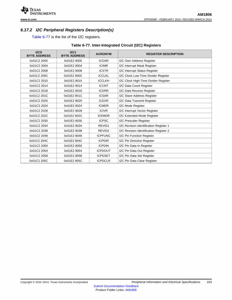
AM1806www.ti.com SPRS658F –FEBRUARY 2010–REVISED MARCH 2014
6.17.2 I2C Peripheral Registers Description(s)Table 6-77 is the list of the I2C registers.
Table 6-77. Inter-Integrated Circuit (I2C) Registers
I2C0 I2C1 ACRONYM REGISTER DESCRIPTIONBYTE ADDRESS BYTE ADDRESS0x01C2 2000 0x01E2 8000 ICOAR I2C Own Address Register0x01C2 2004 0x01E2 8004 ICIMR I2C Interrupt Mask Register0x01C2 2008 0x01E2 8008 ICSTR I2C Interrupt Status Register0x01C2 200C 0x01E2 800C ICCLKL I2C Clock Low-Time Divider Register0x01C2 2010 0x01E2 8010 ICCLKH I2C Clock High-Time Divider Register0x01C2 2014 0x01E2 8014 ICCNT I2C Data Count Register0x01C2 2018 0x01E2 8018 ICDRR I2C Data Receive Register0x01C2 201C 0x01E2 801C ICSAR I2C Slave Address Register0x01C2 2020 0x01E2 8020 ICDXR I2C Data Transmit Register0x01C2 2024 0x01E2 8024 ICMDR I2C Mode Register0x01C2 2028 0x01E2 8028 ICIVR I2C Interrupt Vector Register0x01C2 202C 0x01E2 802C ICEMDR I2C Extended Mode Register0x01C2 2030 0x01E2 8030 ICPSC I2C Prescaler Register0x01C2 2034 0x01E2 8034 REVID1 I2C Revision Identification Register 10x01C2 2038 0x01E2 8038 REVID2 I2C Revision Identification Register 20x01C2 2048 0x01E2 8048 ICPFUNC I2C Pin Function Register0x01C2 204C 0x01E2 804C ICPDIR I2C Pin Direction Register0x01C2 2050 0x01E2 8050 ICPDIN I2C Pin Data In Register0x01C2 2054 0x01E2 8054 ICPDOUT I2C Pin Data Out Register0x01C2 2058 0x01E2 8058 ICPDSET I2C Pin Data Set Register0x01C2 205C 0x01E2 805C ICPDCLR I2C Pin Data Clear Register
Copyright © 2010–2014, Texas Instruments Incorporated Peripheral Information and Electrical Specifications 163Submit Documentation Feedback
Product Folder Links: AM1806
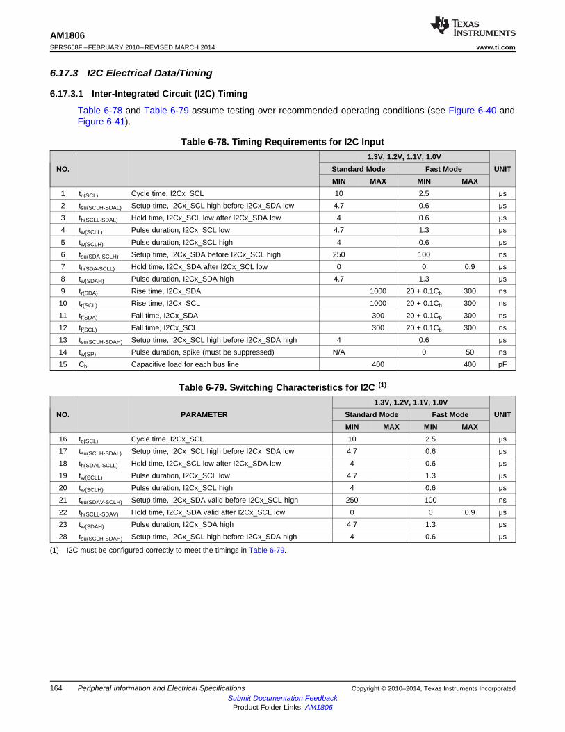
AM1806SPRS658F –FEBRUARY 2010–REVISED MARCH 2014 www.ti.com
6.17.3 I2C Electrical Data/Timing
6.17.3.1 Inter-Integrated Circuit (I2C) Timing
Table 6-78 and Table 6-79 assume testing over recommended operating conditions (see Figure 6-40 andFigure 6-41).
Table 6-78. Timing Requirements for I2C Input1.3V, 1.2V, 1.1V, 1.0V
NO. Standard Mode Fast Mode UNITMIN MAX MIN MAX
1 tc(SCL) Cycle time, I2Cx_SCL 10 2.5 μs2 tsu(SCLH-SDAL) Setup time, I2Cx_SCL high before I2Cx_SDA low 4.7 0.6 μs3 th(SCLL-SDAL) Hold time, I2Cx_SCL low after I2Cx_SDA low 4 0.6 μs4 tw(SCLL) Pulse duration, I2Cx_SCL low 4.7 1.3 μs5 tw(SCLH) Pulse duration, I2Cx_SCL high 4 0.6 μs6 tsu(SDA-SCLH) Setup time, I2Cx_SDA before I2Cx_SCL high 250 100 ns7 th(SDA-SCLL) Hold time, I2Cx_SDA after I2Cx_SCL low 0 0 0.9 μs8 tw(SDAH) Pulse duration, I2Cx_SDA high 4.7 1.3 μs9 tr(SDA) Rise time, I2Cx_SDA 1000 20 + 0.1Cb 300 ns10 tr(SCL) Rise time, I2Cx_SCL 1000 20 + 0.1Cb 300 ns11 tf(SDA) Fall time, I2Cx_SDA 300 20 + 0.1Cb 300 ns12 tf(SCL) Fall time, I2Cx_SCL 300 20 + 0.1Cb 300 ns13 tsu(SCLH-SDAH) Setup time, I2Cx_SCL high before I2Cx_SDA high 4 0.6 μs14 tw(SP) Pulse duration, spike (must be suppressed) N/A 0 50 ns15 Cb Capacitive load for each bus line 400 400 pF
Table 6-79. Switching Characteristics for I2C (1)
1.3V, 1.2V, 1.1V, 1.0VNO. PARAMETER Standard Mode Fast Mode UNIT
MIN MAX MIN MAX16 tc(SCL) Cycle time, I2Cx_SCL 10 2.5 μs17 tsu(SCLH-SDAL) Setup time, I2Cx_SCL high before I2Cx_SDA low 4.7 0.6 μs18 th(SDAL-SCLL) Hold time, I2Cx_SCL low after I2Cx_SDA low 4 0.6 μs19 tw(SCLL) Pulse duration, I2Cx_SCL low 4.7 1.3 μs20 tw(SCLH) Pulse duration, I2Cx_SCL high 4 0.6 μs21 tsu(SDAV-SCLH) Setup time, I2Cx_SDA valid before I2Cx_SCL high 250 100 ns22 th(SCLL-SDAV) Hold time, I2Cx_SDA valid after I2Cx_SCL low 0 0 0.9 μs23 tw(SDAH) Pulse duration, I2Cx_SDA high 4.7 1.3 μs28 tsu(SCLH-SDAH) Setup time, I2Cx_SCL high before I2Cx_SDA high 4 0.6 μs
(1) I2C must be configured correctly to meet the timings in Table 6-79.
164 Peripheral Information and Electrical Specifications Copyright © 2010–2014, Texas Instruments IncorporatedSubmit Documentation Feedback
Product Folder Links: AM1806
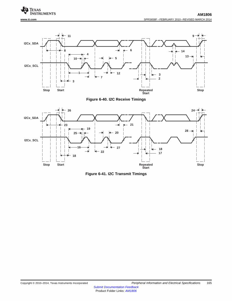
25
2319
1822
27
20
21
1718
28
Stop Start RepeatedStart
Stop
I2Cx_SDA
I2Cx_SCL
16
26 24
10
84
37
12
5
6 14
23
13
Stop Start RepeatedStart
Stop
I2Cx_SDA
I2Cx_SCL
1
11 9
AM1806www.ti.com SPRS658F –FEBRUARY 2010–REVISED MARCH 2014
Figure 6-40. I2C Receive Timings
Figure 6-41. I2C Transmit Timings
Copyright © 2010–2014, Texas Instruments Incorporated Peripheral Information and Electrical Specifications 165Submit Documentation Feedback
Product Folder Links: AM1806
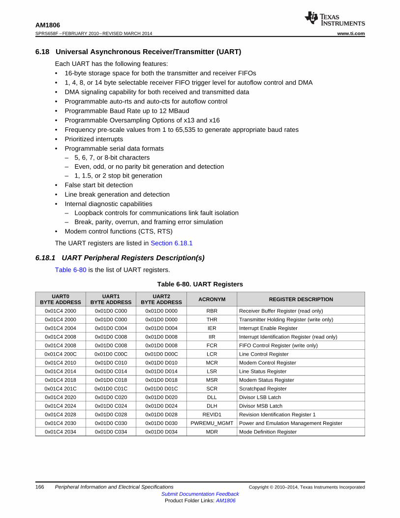
AM1806SPRS658F –FEBRUARY 2010–REVISED MARCH 2014 www.ti.com
6.18 Universal Asynchronous Receiver/Transmitter (UART)Each UART has the following features:• 16-byte storage space for both the transmitter and receiver FIFOs• 1, 4, 8, or 14 byte selectable receiver FIFO trigger level for autoflow control and DMA• DMA signaling capability for both received and transmitted data• Programmable auto-rts and auto-cts for autoflow control• Programmable Baud Rate up to 12 MBaud• Programmable Oversampling Options of x13 and x16• Frequency pre-scale values from 1 to 65,535 to generate appropriate baud rates• Prioritized interrupts• Programmable serial data formats
– 5, 6, 7, or 8-bit characters– Even, odd, or no parity bit generation and detection– 1, 1.5, or 2 stop bit generation
• False start bit detection• Line break generation and detection• Internal diagnostic capabilities
– Loopback controls for communications link fault isolation– Break, parity, overrun, and framing error simulation
• Modem control functions (CTS, RTS)
The UART registers are listed in Section 6.18.1
6.18.1 UART Peripheral Registers Description(s)Table 6-80 is the list of UART registers.
Table 6-80. UART Registers
UART0 UART1 UART2 ACRONYM REGISTER DESCRIPTIONBYTE ADDRESS BYTE ADDRESS BYTE ADDRESS0x01C4 2000 0x01D0 C000 0x01D0 D000 RBR Receiver Buffer Register (read only)0x01C4 2000 0x01D0 C000 0x01D0 D000 THR Transmitter Holding Register (write only)0x01C4 2004 0x01D0 C004 0x01D0 D004 IER Interrupt Enable Register0x01C4 2008 0x01D0 C008 0x01D0 D008 IIR Interrupt Identification Register (read only)0x01C4 2008 0x01D0 C008 0x01D0 D008 FCR FIFO Control Register (write only)0x01C4 200C 0x01D0 C00C 0x01D0 D00C LCR Line Control Register0x01C4 2010 0x01D0 C010 0x01D0 D010 MCR Modem Control Register0x01C4 2014 0x01D0 C014 0x01D0 D014 LSR Line Status Register0x01C4 2018 0x01D0 C018 0x01D0 D018 MSR Modem Status Register0x01C4 201C 0x01D0 C01C 0x01D0 D01C SCR Scratchpad Register0x01C4 2020 0x01D0 C020 0x01D0 D020 DLL Divisor LSB Latch0x01C4 2024 0x01D0 C024 0x01D0 D024 DLH Divisor MSB Latch0x01C4 2028 0x01D0 C028 0x01D0 D028 REVID1 Revision Identification Register 10x01C4 2030 0x01D0 C030 0x01D0 D030 PWREMU_MGMT Power and Emulation Management Register0x01C4 2034 0x01D0 C034 0x01D0 D034 MDR Mode Definition Register
166 Peripheral Information and Electrical Specifications Copyright © 2010–2014, Texas Instruments IncorporatedSubmit Documentation Feedback
Product Folder Links: AM1806
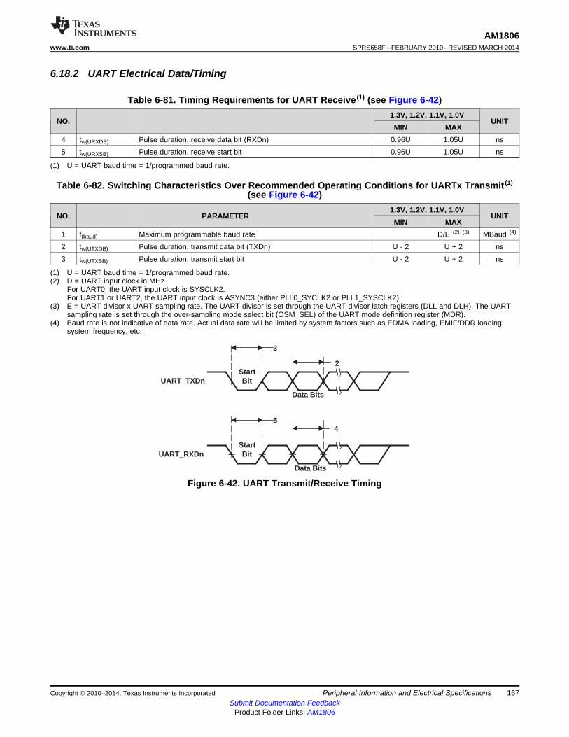
3
2StartBit
Data Bits
UART_TXDn
UART_RXDn
5
Data Bits
BitStart
4
AM1806www.ti.com SPRS658F –FEBRUARY 2010–REVISED MARCH 2014
6.18.2 UART Electrical Data/Timing
Table 6-81. Timing Requirements for UART Receive (1) (see Figure 6-42)1.3V, 1.2V, 1.1V, 1.0V
NO. UNITMIN MAX
4 tw(URXDB) Pulse duration, receive data bit (RXDn) 0.96U 1.05U ns5 tw(URXSB) Pulse duration, receive start bit 0.96U 1.05U ns
(1) U = UART baud time = 1/programmed baud rate.
Table 6-82. Switching Characteristics Over Recommended Operating Conditions for UARTx Transmit (1)
(see Figure 6-42)1.3V, 1.2V, 1.1V, 1.0V
NO. PARAMETER UNITMIN MAX
1 f(baud) Maximum programmable baud rate D/E (2) (3) MBaud (4)
2 tw(UTXDB) Pulse duration, transmit data bit (TXDn) U - 2 U + 2 ns3 tw(UTXSB) Pulse duration, transmit start bit U - 2 U + 2 ns
(1) U = UART baud time = 1/programmed baud rate.(2) D = UART input clock in MHz.
For UART0, the UART input clock is SYSCLK2.For UART1 or UART2, the UART input clock is ASYNC3 (either PLL0_SYCLK2 or PLL1_SYSCLK2).
(3) E = UART divisor x UART sampling rate. The UART divisor is set through the UART divisor latch registers (DLL and DLH). The UARTsampling rate is set through the over-sampling mode select bit (OSM_SEL) of the UART mode definition register (MDR).
(4) Baud rate is not indicative of data rate. Actual data rate will be limited by system factors such as EDMA loading, EMIF/DDR loading,system frequency, etc.
Figure 6-42. UART Transmit/Receive Timing
Copyright © 2010–2014, Texas Instruments Incorporated Peripheral Information and Electrical Specifications 167Submit Documentation Feedback
Product Folder Links: AM1806
AM1806SPRS658F –FEBRUARY 2010–REVISED MARCH 2014 www.ti.com
6.19 Universal Serial Bus OTG Controller (USB0) [USB2.0 OTG]The USB2.0 peripheral supports the following features:• USB 2.0 peripheral at speeds high speed (HS: 480 Mb/s) and full speed (FS: 12 Mb/s)• USB 2.0 host at speeds HS, FS, and low speed (LS: 1.5 Mb/s)• All transfer modes (control, bulk, interrupt, and isochronous)• 4 Transmit (TX) and 4 Receive (RX) endpoints in addition to endpoint 0• FIFO RAM
– 4K endpoint– Programmable size
• Integrated USB 2.0 High Speed PHY• Connects to a standard Charge Pump for VBUS 5 V generation• RNDIS mode for accelerating RNDIS type protocols using short packet termination over USB
Important Notice: The USB0 controller module clock (PLL0_SYSCLK2) must be greater than 30 MHz forproper operation of the USB controller. A clock rate of 60 MHz or greater is recommended to avoid datathroughput reduction.
Table 6-83 is the list of USB OTG registers.
6.19.1 USB Peripheral Registers Description(s)Table 6-83 is the list of the USB0 registers.
Table 6-83. Universal Serial Bus OTG (USB0) Registers
BYTE ADDRESS ACRONYM REGISTER DESCRIPTION0x01E0 0000 REVID Revision Register0x01E0 0004 CTRLR Control Register0x01E0 0008 STATR Status Register0x01E0 000C EMUR Emulation Register0x01E0 0010 MODE Mode Register0x01E0 0014 AUTOREQ Autorequest Register0x01E0 0018 SRPFIXTIME SRP Fix Time Register0x01E0 001C TEARDOWN Teardown Register0x01E0 0020 INTSRCR USB Interrupt Source Register0x01E0 0024 INTSETR USB Interrupt Source Set Register0x01E0 0028 INTCLRR USB Interrupt Source Clear Register0x01E0 002C INTMSKR USB Interrupt Mask Register0x01E0 0030 INTMSKSETR USB Interrupt Mask Set Register0x01E0 0034 INTMSKCLRR USB Interrupt Mask Clear Register0x01E0 0038 INTMASKEDR USB Interrupt Source Masked Register0x01E0 003C EOIR USB End of Interrupt Register0x01E0 0040 - Reserved0x01E0 0050 GENRNDISSZ1 Generic RNDIS Size EP10x01E0 0054 GENRNDISSZ2 Generic RNDIS Size EP20x01E0 0058 GENRNDISSZ3 Generic RNDIS Size EP30x01E0 005C GENRNDISSZ4 Generic RNDIS Size EP40x01E0 0400 FADDR Function Address Register0x01E0 0401 POWER Power Management Register0x01E0 0402 INTRTX Interrupt Register for Endpoint 0 plus Transmit Endpoints 1 to 40x01E0 0404 INTRRX Interrupt Register for Receive Endpoints 1 to 40x01E0 0406 INTRTXE Interrupt enable register for INTRTX
168 Peripheral Information and Electrical Specifications Copyright © 2010–2014, Texas Instruments IncorporatedSubmit Documentation Feedback
Product Folder Links: AM1806
AM1806www.ti.com SPRS658F –FEBRUARY 2010–REVISED MARCH 2014
Table 6-83. Universal Serial Bus OTG (USB0) Registers (continued)BYTE ADDRESS ACRONYM REGISTER DESCRIPTION
0x01E0 0408 INTRRXE Interrupt Enable Register for INTRRX0x01E0 040A INTRUSB Interrupt Register for Common USB Interrupts0x01E0 040B INTRUSBE Interrupt Enable Register for INTRUSB0x01E0 040C FRAME Frame Number Register0x01E0 040E INDEX Index Register for Selecting the Endpoint Status and Control Registers0x01E0 040F TESTMODE Register to Enable the USB 2.0 Test Modes
Indexed RegistersThese registers operate on the endpoint selected by the INDEX register
0x01E0 0410 TXMAXP Maximum Packet Size for Peripheral/Host Transmit Endpoint (Index register set to selectEndpoints 1-4 only)
0x01E0 0412 PERI_CSR0 Control Status Register for Endpoint 0 in Peripheral Mode.(Index register set to select Endpoint 0)
HOST_CSR0 Control Status Register for Endpoint 0 in Host Mode.(Index register set to select Endpoint 0)
PERI_TXCSR Control Status Register for Peripheral Transmit Endpoint.(Index register set to select Endpoints 1-4)
HOST_TXCSR Control Status Register for Host Transmit Endpoint.(Index register set to select Endpoints 1-4)
0x01E0 0414 RXMAXP Maximum Packet Size for Peripheral/Host Receive Endpoint(Index register set to select Endpoints 1-4 only)
0x01E0 0416 PERI_RXCSR Control Status Register for Peripheral Receive Endpoint.(Index register set to select Endpoints 1-4)
HOST_RXCSR Control Status Register for Host Receive Endpoint.(Index register set to select Endpoints 1-4)
0x01E0 0418 COUNT0 Number of Received Bytes in Endpoint 0 FIFO.(Index register set to select Endpoint 0)
RXCOUNT Number of Bytes in Host Receive Endpoint FIFO.(Index register set to select Endpoints 1- 4)
0x01E0 041A HOST_TYPE0 Defines the speed of Endpoint 0HOST_TXTYPE Sets the operating speed, transaction protocol and peripheral endpoint number for the host
Transmit endpoint.(Index register set to select Endpoints 1-4 only)
0x01E0 041B HOST_NAKLIMIT0 Sets the NAK response timeout on Endpoint 0.(Index register set to select Endpoint 0)
HOST_TXINTERVAL Sets the polling interval for Interrupt/ISOC transactions or the NAK response timeout on Bulktransactions for host Transmit endpoint.(Index register set to select Endpoints 1-4 only)
0x01E0 041C HOST_RXTYPE Sets the operating speed, transaction protocol and peripheral endpoint number for the hostReceive endpoint.(Index register set to select Endpoints 1-4 only)
0x01E0 041D HOST_RXINTERVAL Sets the polling interval for Interrupt/ISOC transactions or the NAK response timeout on Bulktransactions for host Receive endpoint.(Index register set to select Endpoints 1-4 only)
0x01E0 041F CONFIGDATA Returns details of core configuration. (Index register set to select Endpoint 0)FIFO
0x01E0 0420 FIFO0 Transmit and Receive FIFO Register for Endpoint 00x01E0 0424 FIFO1 Transmit and Receive FIFO Register for Endpoint 10x01E0 0428 FIFO2 Transmit and Receive FIFO Register for Endpoint 20x01E0 042C FIFO3 Transmit and Receive FIFO Register for Endpoint 30x01E0 0430 FIFO4 Transmit and Receive FIFO Register for Endpoint 4
OTG Device Control0x01E0 0460 DEVCTL Device Control Register
Dynamic FIFO Control
Copyright © 2010–2014, Texas Instruments Incorporated Peripheral Information and Electrical Specifications 169Submit Documentation Feedback
Product Folder Links: AM1806
AM1806SPRS658F –FEBRUARY 2010–REVISED MARCH 2014 www.ti.com
Table 6-83. Universal Serial Bus OTG (USB0) Registers (continued)BYTE ADDRESS ACRONYM REGISTER DESCRIPTION
0x01E0 0462 TXFIFOSZ Transmit Endpoint FIFO Size(Index register set to select Endpoints 1-4 only)
0x01E0 0463 RXFIFOSZ Receive Endpoint FIFO Size(Index register set to select Endpoints 1-4 only)
0x01E0 0464 TXFIFOADDR Transmit Endpoint FIFO Address(Index register set to select Endpoints 1-4 only)
0x01E0 0466 RXFIFOADDR Receive Endpoint FIFO Address(Index register set to select Endpoints 1-4 only)
0x01E0 046C HWVERS Hardware Version RegisterTarget Endpoint 0 Control Registers, Valid Only in Host Mode
0x01E0 0480 TXFUNCADDR Address of the target function that has to be accessed through the associated TransmitEndpoint.
0x01E0 0482 TXHUBADDR Address of the hub that has to be accessed through the associated Transmit Endpoint. This isused only when full speed or low speed device is connected via a USB2.0 high-speed hub.
0x01E0 0483 TXHUBPORT Port of the hub that has to be accessed through the associated Transmit Endpoint. This is usedonly when full speed or low speed device is connected via a USB2.0 high-speed hub.
0x01E0 0484 RXFUNCADDR Address of the target function that has to be accessed through the associated ReceiveEndpoint.
0x01E0 0486 RXHUBADDR Address of the hub that has to be accessed through the associated Receive Endpoint. This isused only when full speed or low speed device is connected via a USB2.0 high-speed hub.
0x01E0 0487 RXHUBPORT Port of the hub that has to be accessed through the associated Receive Endpoint. This is usedonly when full speed or low speed device is connected via a USB2.0 high-speed hub.
Target Endpoint 1 Control Registers, Valid Only in Host Mode0x01E0 0488 TXFUNCADDR Address of the target function that has to be accessed through the associated Transmit
Endpoint.0x01E0 048A TXHUBADDR Address of the hub that has to be accessed through the associated Transmit Endpoint. This is
used only when full speed or low speed device is connected via a USB2.0 high-speed hub.0x01E0 048B TXHUBPORT Port of the hub that has to be accessed through the associated Transmit Endpoint. This is used
only when full speed or low speed device is connected via a USB2.0 high-speed hub.0x01E0 048C RXFUNCADDR Address of the target function that has to be accessed through the associated Receive
Endpoint.0x01E0 048E RXHUBADDR Address of the hub that has to be accessed through the associated Receive Endpoint. This is
used only when full speed or low speed device is connected via a USB2.0 high-speed hub.0x01E0 048F RXHUBPORT Port of the hub that has to be accessed through the associated Receive Endpoint. This is used
only when full speed or low speed device is connected via a USB2.0 high-speed hub.Target Endpoint 2 Control Registers, Valid Only in Host Mode
0x01E0 0490 TXFUNCADDR Address of the target function that has to be accessed through the associated TransmitEndpoint.
0x01E0 0492 TXHUBADDR Address of the hub that has to be accessed through the associated Transmit Endpoint. This isused only when full speed or low speed device is connected via a USB2.0 high-speed hub.
0x01E0 0493 TXHUBPORT Port of the hub that has to be accessed through the associated Transmit Endpoint. This is usedonly when full speed or low speed device is connected via a USB2.0 high-speed hub.
0x01E0 0494 RXFUNCADDR Address of the target function that has to be accessed through the associated ReceiveEndpoint.
0x01E0 0496 RXHUBADDR Address of the hub that has to be accessed through the associated Receive Endpoint. This isused only when full speed or low speed device is connected via a USB2.0 high-speed hub.
0x01E0 0497 RXHUBPORT Port of the hub that has to be accessed through the associated Receive Endpoint. This is usedonly when full speed or low speed device is connected via a USB2.0 high-speed hub.
Target Endpoint 3 Control Registers, Valid Only in Host Mode0x01E0 0498 TXFUNCADDR Address of the target function that has to be accessed through the associated Transmit
Endpoint.0x01E0 049A TXHUBADDR Address of the hub that has to be accessed through the associated Transmit Endpoint. This is
used only when full speed or low speed device is connected via a USB2.0 high-speed hub.0x01E0 049B TXHUBPORT Port of the hub that has to be accessed through the associated Transmit Endpoint. This is used
only when full speed or low speed device is connected via a USB2.0 high-speed hub.
170 Peripheral Information and Electrical Specifications Copyright © 2010–2014, Texas Instruments IncorporatedSubmit Documentation Feedback
Product Folder Links: AM1806
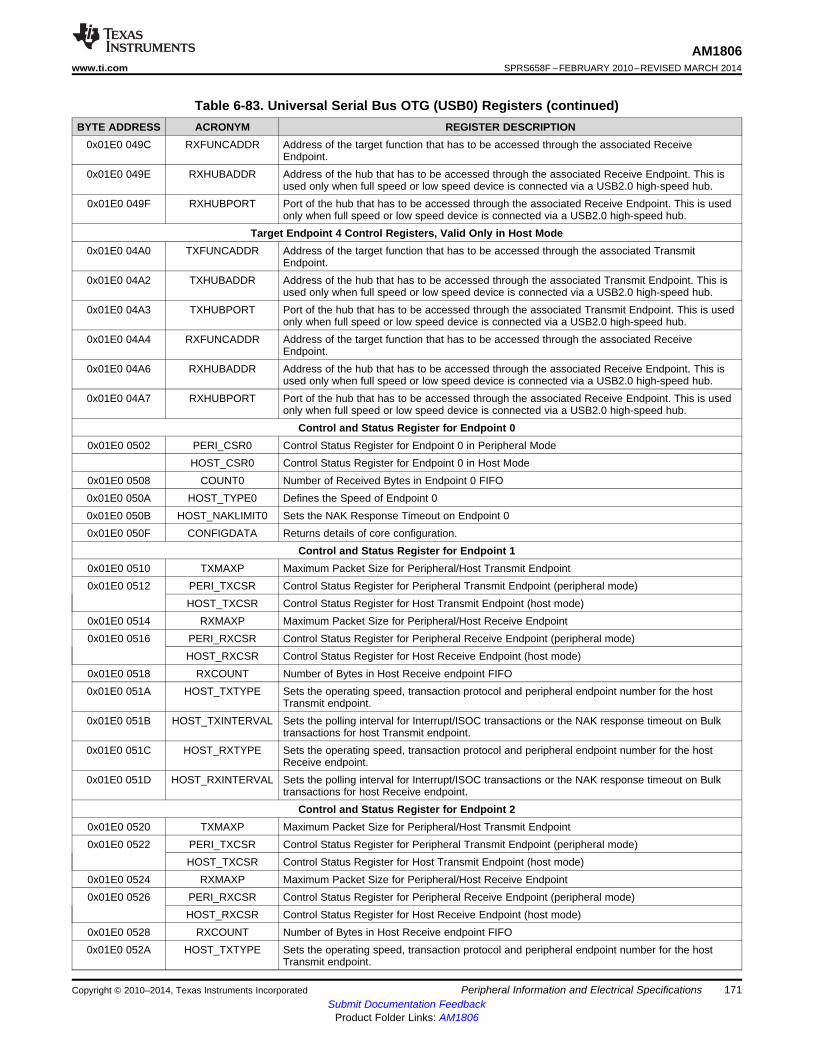
AM1806www.ti.com SPRS658F –FEBRUARY 2010–REVISED MARCH 2014
Table 6-83. Universal Serial Bus OTG (USB0) Registers (continued)BYTE ADDRESS ACRONYM REGISTER DESCRIPTION
0x01E0 049C RXFUNCADDR Address of the target function that has to be accessed through the associated ReceiveEndpoint.
0x01E0 049E RXHUBADDR Address of the hub that has to be accessed through the associated Receive Endpoint. This isused only when full speed or low speed device is connected via a USB2.0 high-speed hub.
0x01E0 049F RXHUBPORT Port of the hub that has to be accessed through the associated Receive Endpoint. This is usedonly when full speed or low speed device is connected via a USB2.0 high-speed hub.
Target Endpoint 4 Control Registers, Valid Only in Host Mode0x01E0 04A0 TXFUNCADDR Address of the target function that has to be accessed through the associated Transmit
Endpoint.0x01E0 04A2 TXHUBADDR Address of the hub that has to be accessed through the associated Transmit Endpoint. This is
used only when full speed or low speed device is connected via a USB2.0 high-speed hub.0x01E0 04A3 TXHUBPORT Port of the hub that has to be accessed through the associated Transmit Endpoint. This is used
only when full speed or low speed device is connected via a USB2.0 high-speed hub.0x01E0 04A4 RXFUNCADDR Address of the target function that has to be accessed through the associated Receive
Endpoint.0x01E0 04A6 RXHUBADDR Address of the hub that has to be accessed through the associated Receive Endpoint. This is
used only when full speed or low speed device is connected via a USB2.0 high-speed hub.0x01E0 04A7 RXHUBPORT Port of the hub that has to be accessed through the associated Receive Endpoint. This is used
only when full speed or low speed device is connected via a USB2.0 high-speed hub.Control and Status Register for Endpoint 0
0x01E0 0502 PERI_CSR0 Control Status Register for Endpoint 0 in Peripheral ModeHOST_CSR0 Control Status Register for Endpoint 0 in Host Mode
0x01E0 0508 COUNT0 Number of Received Bytes in Endpoint 0 FIFO0x01E0 050A HOST_TYPE0 Defines the Speed of Endpoint 00x01E0 050B HOST_NAKLIMIT0 Sets the NAK Response Timeout on Endpoint 00x01E0 050F CONFIGDATA Returns details of core configuration.
Control and Status Register for Endpoint 10x01E0 0510 TXMAXP Maximum Packet Size for Peripheral/Host Transmit Endpoint0x01E0 0512 PERI_TXCSR Control Status Register for Peripheral Transmit Endpoint (peripheral mode)
HOST_TXCSR Control Status Register for Host Transmit Endpoint (host mode)0x01E0 0514 RXMAXP Maximum Packet Size for Peripheral/Host Receive Endpoint0x01E0 0516 PERI_RXCSR Control Status Register for Peripheral Receive Endpoint (peripheral mode)
HOST_RXCSR Control Status Register for Host Receive Endpoint (host mode)0x01E0 0518 RXCOUNT Number of Bytes in Host Receive endpoint FIFO0x01E0 051A HOST_TXTYPE Sets the operating speed, transaction protocol and peripheral endpoint number for the host
Transmit endpoint.0x01E0 051B HOST_TXINTERVAL Sets the polling interval for Interrupt/ISOC transactions or the NAK response timeout on Bulk
transactions for host Transmit endpoint.0x01E0 051C HOST_RXTYPE Sets the operating speed, transaction protocol and peripheral endpoint number for the host
Receive endpoint.0x01E0 051D HOST_RXINTERVAL Sets the polling interval for Interrupt/ISOC transactions or the NAK response timeout on Bulk
transactions for host Receive endpoint.Control and Status Register for Endpoint 2
0x01E0 0520 TXMAXP Maximum Packet Size for Peripheral/Host Transmit Endpoint0x01E0 0522 PERI_TXCSR Control Status Register for Peripheral Transmit Endpoint (peripheral mode)
HOST_TXCSR Control Status Register for Host Transmit Endpoint (host mode)0x01E0 0524 RXMAXP Maximum Packet Size for Peripheral/Host Receive Endpoint0x01E0 0526 PERI_RXCSR Control Status Register for Peripheral Receive Endpoint (peripheral mode)
HOST_RXCSR Control Status Register for Host Receive Endpoint (host mode)0x01E0 0528 RXCOUNT Number of Bytes in Host Receive endpoint FIFO0x01E0 052A HOST_TXTYPE Sets the operating speed, transaction protocol and peripheral endpoint number for the host
Transmit endpoint.
Copyright © 2010–2014, Texas Instruments Incorporated Peripheral Information and Electrical Specifications 171Submit Documentation Feedback
Product Folder Links: AM1806
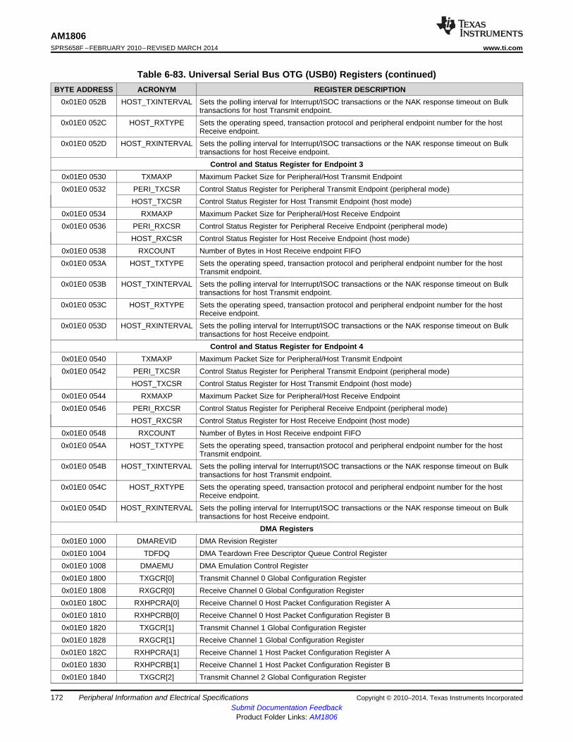
AM1806SPRS658F –FEBRUARY 2010–REVISED MARCH 2014 www.ti.com
Table 6-83. Universal Serial Bus OTG (USB0) Registers (continued)BYTE ADDRESS ACRONYM REGISTER DESCRIPTION
0x01E0 052B HOST_TXINTERVAL Sets the polling interval for Interrupt/ISOC transactions or the NAK response timeout on Bulktransactions for host Transmit endpoint.
0x01E0 052C HOST_RXTYPE Sets the operating speed, transaction protocol and peripheral endpoint number for the hostReceive endpoint.
0x01E0 052D HOST_RXINTERVAL Sets the polling interval for Interrupt/ISOC transactions or the NAK response timeout on Bulktransactions for host Receive endpoint.
Control and Status Register for Endpoint 30x01E0 0530 TXMAXP Maximum Packet Size for Peripheral/Host Transmit Endpoint0x01E0 0532 PERI_TXCSR Control Status Register for Peripheral Transmit Endpoint (peripheral mode)
HOST_TXCSR Control Status Register for Host Transmit Endpoint (host mode)0x01E0 0534 RXMAXP Maximum Packet Size for Peripheral/Host Receive Endpoint0x01E0 0536 PERI_RXCSR Control Status Register for Peripheral Receive Endpoint (peripheral mode)
HOST_RXCSR Control Status Register for Host Receive Endpoint (host mode)0x01E0 0538 RXCOUNT Number of Bytes in Host Receive endpoint FIFO0x01E0 053A HOST_TXTYPE Sets the operating speed, transaction protocol and peripheral endpoint number for the host
Transmit endpoint.0x01E0 053B HOST_TXINTERVAL Sets the polling interval for Interrupt/ISOC transactions or the NAK response timeout on Bulk
transactions for host Transmit endpoint.0x01E0 053C HOST_RXTYPE Sets the operating speed, transaction protocol and peripheral endpoint number for the host
Receive endpoint.0x01E0 053D HOST_RXINTERVAL Sets the polling interval for Interrupt/ISOC transactions or the NAK response timeout on Bulk
transactions for host Receive endpoint.Control and Status Register for Endpoint 4
0x01E0 0540 TXMAXP Maximum Packet Size for Peripheral/Host Transmit Endpoint0x01E0 0542 PERI_TXCSR Control Status Register for Peripheral Transmit Endpoint (peripheral mode)
HOST_TXCSR Control Status Register for Host Transmit Endpoint (host mode)0x01E0 0544 RXMAXP Maximum Packet Size for Peripheral/Host Receive Endpoint0x01E0 0546 PERI_RXCSR Control Status Register for Peripheral Receive Endpoint (peripheral mode)
HOST_RXCSR Control Status Register for Host Receive Endpoint (host mode)0x01E0 0548 RXCOUNT Number of Bytes in Host Receive endpoint FIFO0x01E0 054A HOST_TXTYPE Sets the operating speed, transaction protocol and peripheral endpoint number for the host
Transmit endpoint.0x01E0 054B HOST_TXINTERVAL Sets the polling interval for Interrupt/ISOC transactions or the NAK response timeout on Bulk
transactions for host Transmit endpoint.0x01E0 054C HOST_RXTYPE Sets the operating speed, transaction protocol and peripheral endpoint number for the host
Receive endpoint.0x01E0 054D HOST_RXINTERVAL Sets the polling interval for Interrupt/ISOC transactions or the NAK response timeout on Bulk
transactions for host Receive endpoint.DMA Registers
0x01E0 1000 DMAREVID DMA Revision Register0x01E0 1004 TDFDQ DMA Teardown Free Descriptor Queue Control Register0x01E0 1008 DMAEMU DMA Emulation Control Register0x01E0 1800 TXGCR[0] Transmit Channel 0 Global Configuration Register0x01E0 1808 RXGCR[0] Receive Channel 0 Global Configuration Register0x01E0 180C RXHPCRA[0] Receive Channel 0 Host Packet Configuration Register A0x01E0 1810 RXHPCRB[0] Receive Channel 0 Host Packet Configuration Register B0x01E0 1820 TXGCR[1] Transmit Channel 1 Global Configuration Register0x01E0 1828 RXGCR[1] Receive Channel 1 Global Configuration Register0x01E0 182C RXHPCRA[1] Receive Channel 1 Host Packet Configuration Register A0x01E0 1830 RXHPCRB[1] Receive Channel 1 Host Packet Configuration Register B0x01E0 1840 TXGCR[2] Transmit Channel 2 Global Configuration Register
172 Peripheral Information and Electrical Specifications Copyright © 2010–2014, Texas Instruments IncorporatedSubmit Documentation Feedback
Product Folder Links: AM1806
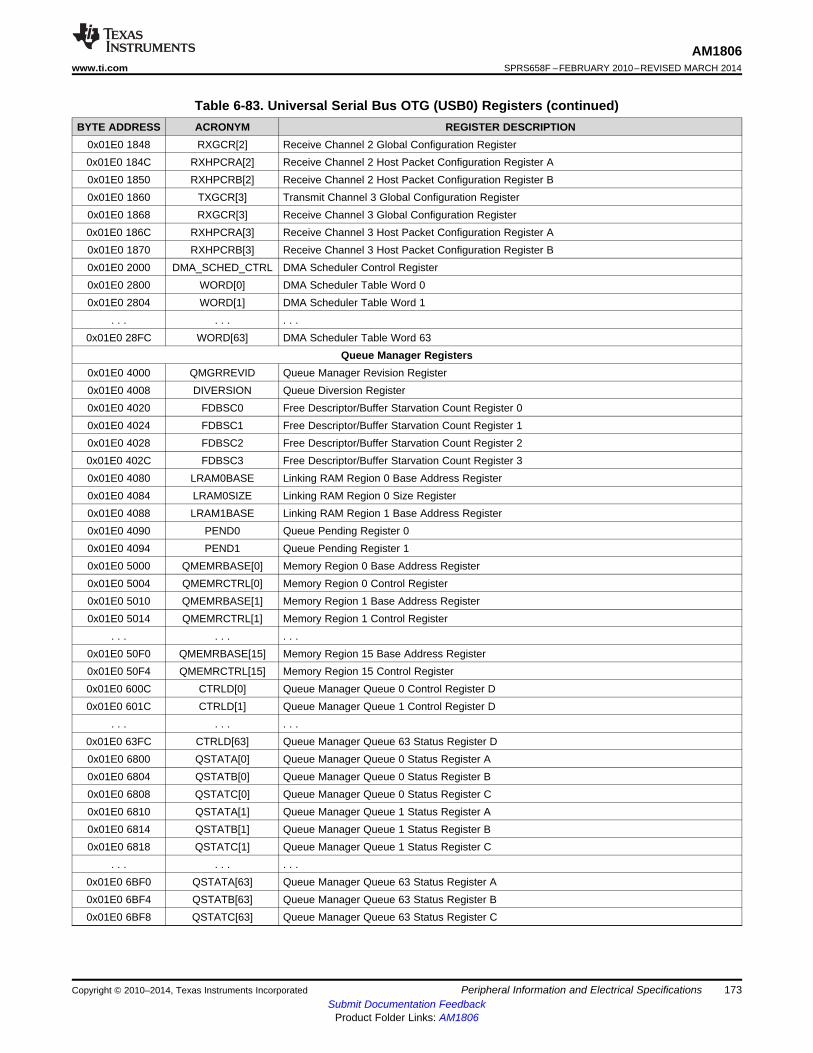
AM1806www.ti.com SPRS658F –FEBRUARY 2010–REVISED MARCH 2014
Table 6-83. Universal Serial Bus OTG (USB0) Registers (continued)BYTE ADDRESS ACRONYM REGISTER DESCRIPTION
0x01E0 1848 RXGCR[2] Receive Channel 2 Global Configuration Register0x01E0 184C RXHPCRA[2] Receive Channel 2 Host Packet Configuration Register A0x01E0 1850 RXHPCRB[2] Receive Channel 2 Host Packet Configuration Register B0x01E0 1860 TXGCR[3] Transmit Channel 3 Global Configuration Register0x01E0 1868 RXGCR[3] Receive Channel 3 Global Configuration Register0x01E0 186C RXHPCRA[3] Receive Channel 3 Host Packet Configuration Register A0x01E0 1870 RXHPCRB[3] Receive Channel 3 Host Packet Configuration Register B0x01E0 2000 DMA_SCHED_CTRL DMA Scheduler Control Register0x01E0 2800 WORD[0] DMA Scheduler Table Word 00x01E0 2804 WORD[1] DMA Scheduler Table Word 1
. . . . . . . . .0x01E0 28FC WORD[63] DMA Scheduler Table Word 63
Queue Manager Registers0x01E0 4000 QMGRREVID Queue Manager Revision Register0x01E0 4008 DIVERSION Queue Diversion Register0x01E0 4020 FDBSC0 Free Descriptor/Buffer Starvation Count Register 00x01E0 4024 FDBSC1 Free Descriptor/Buffer Starvation Count Register 10x01E0 4028 FDBSC2 Free Descriptor/Buffer Starvation Count Register 20x01E0 402C FDBSC3 Free Descriptor/Buffer Starvation Count Register 30x01E0 4080 LRAM0BASE Linking RAM Region 0 Base Address Register0x01E0 4084 LRAM0SIZE Linking RAM Region 0 Size Register0x01E0 4088 LRAM1BASE Linking RAM Region 1 Base Address Register0x01E0 4090 PEND0 Queue Pending Register 00x01E0 4094 PEND1 Queue Pending Register 10x01E0 5000 QMEMRBASE[0] Memory Region 0 Base Address Register0x01E0 5004 QMEMRCTRL[0] Memory Region 0 Control Register0x01E0 5010 QMEMRBASE[1] Memory Region 1 Base Address Register0x01E0 5014 QMEMRCTRL[1] Memory Region 1 Control Register
. . . . . . . . .0x01E0 50F0 QMEMRBASE[15] Memory Region 15 Base Address Register0x01E0 50F4 QMEMRCTRL[15] Memory Region 15 Control Register0x01E0 600C CTRLD[0] Queue Manager Queue 0 Control Register D0x01E0 601C CTRLD[1] Queue Manager Queue 1 Control Register D
. . . . . . . . .0x01E0 63FC CTRLD[63] Queue Manager Queue 63 Status Register D0x01E0 6800 QSTATA[0] Queue Manager Queue 0 Status Register A0x01E0 6804 QSTATB[0] Queue Manager Queue 0 Status Register B0x01E0 6808 QSTATC[0] Queue Manager Queue 0 Status Register C0x01E0 6810 QSTATA[1] Queue Manager Queue 1 Status Register A0x01E0 6814 QSTATB[1] Queue Manager Queue 1 Status Register B0x01E0 6818 QSTATC[1] Queue Manager Queue 1 Status Register C
. . . . . . . . .0x01E0 6BF0 QSTATA[63] Queue Manager Queue 63 Status Register A0x01E0 6BF4 QSTATB[63] Queue Manager Queue 63 Status Register B0x01E0 6BF8 QSTATC[63] Queue Manager Queue 63 Status Register C
Copyright © 2010–2014, Texas Instruments Incorporated Peripheral Information and Electrical Specifications 173Submit Documentation Feedback
Product Folder Links: AM1806
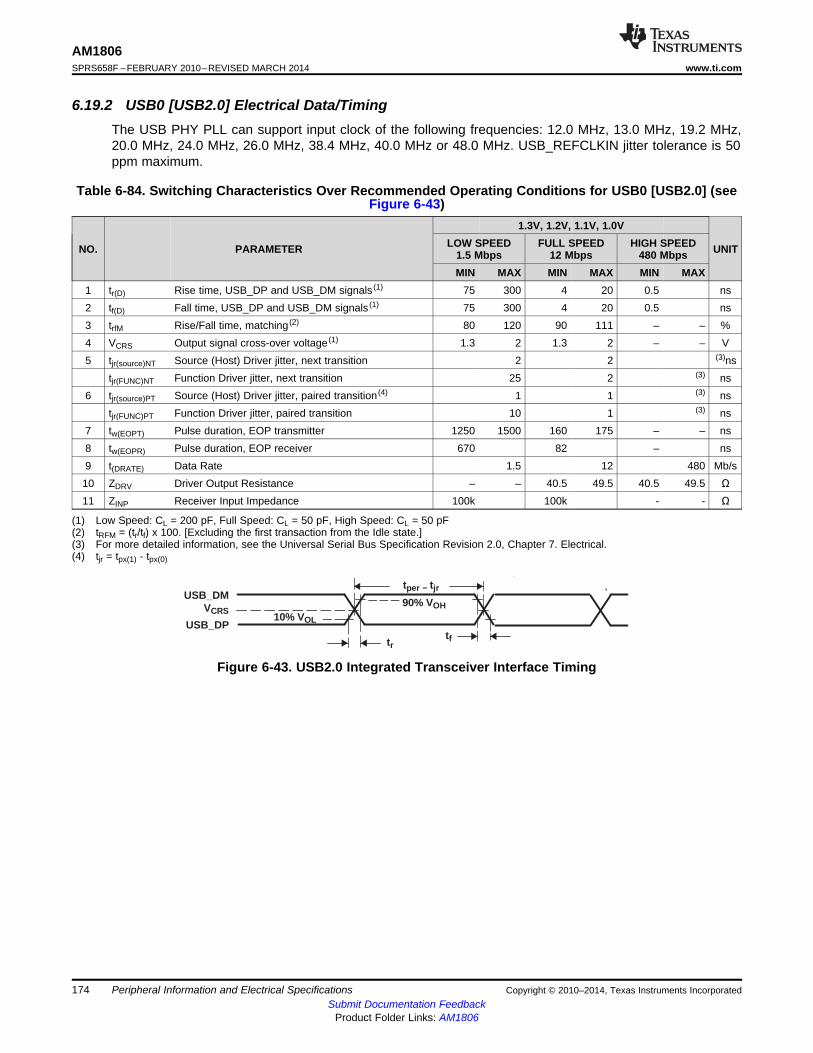
trtf
VCRS90% VOH
10% VOL
USB_DM
USB_DP
tper − tjr
AM1806SPRS658F –FEBRUARY 2010–REVISED MARCH 2014 www.ti.com
6.19.2 USB0 [USB2.0] Electrical Data/TimingThe USB PHY PLL can support input clock of the following frequencies: 12.0 MHz, 13.0 MHz, 19.2 MHz,20.0 MHz, 24.0 MHz, 26.0 MHz, 38.4 MHz, 40.0 MHz or 48.0 MHz. USB_REFCLKIN jitter tolerance is 50ppm maximum.
Table 6-84. Switching Characteristics Over Recommended Operating Conditions for USB0 [USB2.0] (seeFigure 6-43)
1.3V, 1.2V, 1.1V, 1.0VLOW SPEED FULL SPEED HIGH SPEEDNO. PARAMETER UNIT1.5 Mbps 12 Mbps 480 Mbps
MIN MAX MIN MAX MIN MAX1 tr(D) Rise time, USB_DP and USB_DM signals (1) 75 300 4 20 0.5 ns2 tf(D) Fall time, USB_DP and USB_DM signals (1) 75 300 4 20 0.5 ns3 trfM Rise/Fall time, matching (2) 80 120 90 111 – – %4 VCRS Output signal cross-over voltage (1) 1.3 2 1.3 2 – – V5 tjr(source)NT Source (Host) Driver jitter, next transition 2 2 (3)ns
tjr(FUNC)NT Function Driver jitter, next transition 25 2 (3) ns6 tjr(source)PT Source (Host) Driver jitter, paired transition (4) 1 1 (3) ns
tjr(FUNC)PT Function Driver jitter, paired transition 10 1 (3) ns7 tw(EOPT) Pulse duration, EOP transmitter 1250 1500 160 175 – – ns8 tw(EOPR) Pulse duration, EOP receiver 670 82 – ns9 t(DRATE) Data Rate 1.5 12 480 Mb/s10 ZDRV Driver Output Resistance – – 40.5 49.5 40.5 49.5 Ω11 ZINP Receiver Input Impedance 100k 100k - - Ω
(1) Low Speed: CL = 200 pF, Full Speed: CL = 50 pF, High Speed: CL = 50 pF(2) tRFM = (tr/tf) x 100. [Excluding the first transaction from the Idle state.](3) For more detailed information, see the Universal Serial Bus Specification Revision 2.0, Chapter 7. Electrical.(4) tjr = tpx(1) - tpx(0)
Figure 6-43. USB2.0 Integrated Transceiver Interface Timing
174 Peripheral Information and Electrical Specifications Copyright © 2010–2014, Texas Instruments IncorporatedSubmit Documentation Feedback
Product Folder Links: AM1806
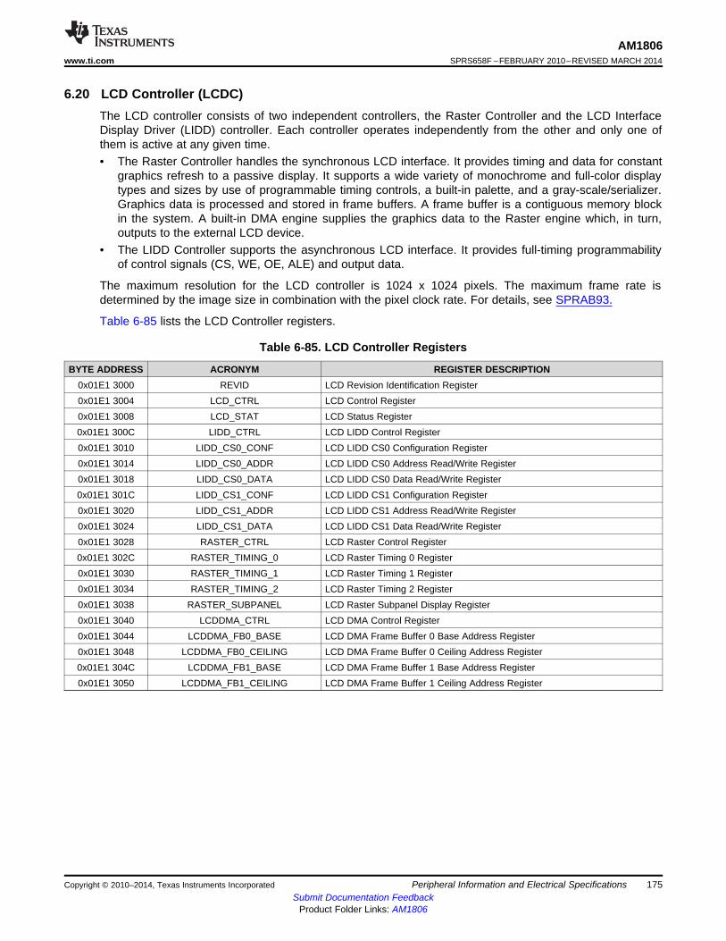
AM1806www.ti.com SPRS658F –FEBRUARY 2010–REVISED MARCH 2014
6.20 LCD Controller (LCDC)The LCD controller consists of two independent controllers, the Raster Controller and the LCD InterfaceDisplay Driver (LIDD) controller. Each controller operates independently from the other and only one ofthem is active at any given time.• The Raster Controller handles the synchronous LCD interface. It provides timing and data for constant
graphics refresh to a passive display. It supports a wide variety of monochrome and full-color displaytypes and sizes by use of programmable timing controls, a built-in palette, and a gray-scale/serializer.Graphics data is processed and stored in frame buffers. A frame buffer is a contiguous memory blockin the system. A built-in DMA engine supplies the graphics data to the Raster engine which, in turn,outputs to the external LCD device.
• The LIDD Controller supports the asynchronous LCD interface. It provides full-timing programmabilityof control signals (CS, WE, OE, ALE) and output data.
The maximum resolution for the LCD controller is 1024 x 1024 pixels. The maximum frame rate isdetermined by the image size in combination with the pixel clock rate. For details, see SPRAB93.
Table 6-85 lists the LCD Controller registers.
Table 6-85. LCD Controller Registers
BYTE ADDRESS ACRONYM REGISTER DESCRIPTION0x01E1 3000 REVID LCD Revision Identification Register0x01E1 3004 LCD_CTRL LCD Control Register0x01E1 3008 LCD_STAT LCD Status Register0x01E1 300C LIDD_CTRL LCD LIDD Control Register0x01E1 3010 LIDD_CS0_CONF LCD LIDD CS0 Configuration Register0x01E1 3014 LIDD_CS0_ADDR LCD LIDD CS0 Address Read/Write Register0x01E1 3018 LIDD_CS0_DATA LCD LIDD CS0 Data Read/Write Register0x01E1 301C LIDD_CS1_CONF LCD LIDD CS1 Configuration Register0x01E1 3020 LIDD_CS1_ADDR LCD LIDD CS1 Address Read/Write Register0x01E1 3024 LIDD_CS1_DATA LCD LIDD CS1 Data Read/Write Register0x01E1 3028 RASTER_CTRL LCD Raster Control Register0x01E1 302C RASTER_TIMING_0 LCD Raster Timing 0 Register0x01E1 3030 RASTER_TIMING_1 LCD Raster Timing 1 Register0x01E1 3034 RASTER_TIMING_2 LCD Raster Timing 2 Register0x01E1 3038 RASTER_SUBPANEL LCD Raster Subpanel Display Register0x01E1 3040 LCDDMA_CTRL LCD DMA Control Register0x01E1 3044 LCDDMA_FB0_BASE LCD DMA Frame Buffer 0 Base Address Register0x01E1 3048 LCDDMA_FB0_CEILING LCD DMA Frame Buffer 0 Ceiling Address Register0x01E1 304C LCDDMA_FB1_BASE LCD DMA Frame Buffer 1 Base Address Register0x01E1 3050 LCDDMA_FB1_CEILING LCD DMA Frame Buffer 1 Ceiling Address Register
Copyright © 2010–2014, Texas Instruments Incorporated Peripheral Information and Electrical Specifications 175Submit Documentation Feedback
Product Folder Links: AM1806
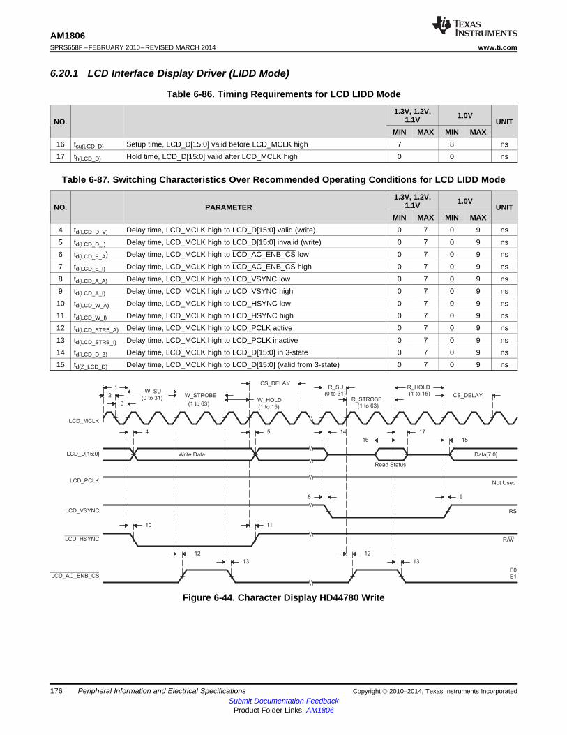
LCD_AC_ENB_CS
LCD_PCLK
2
3
1W_SU
(0 to 31) W_STROBE
(1 to 63)W_HOLD
(1 to 15)
CS_DELAYR_SU
(0 to 31)R_STROBE
(1 to 63)
R_HOLD(1 to 15) CS_DELAY
LCD_MCLK
4
Write Data
5 14
16
17
15
Data[7:0]
Not Used
8 9
10 11
12
13
12
13
RS
R/W
E0E1
LCD_D[15:0]
LCD_VSYNC
LCD_HSYNC
Read Status
AM1806SPRS658F –FEBRUARY 2010–REVISED MARCH 2014 www.ti.com
6.20.1 LCD Interface Display Driver (LIDD Mode)
Table 6-86. Timing Requirements for LCD LIDD Mode
1.3V, 1.2V, 1.0V1.1VNO. UNITMIN MAX MIN MAX
16 tsu(LCD_D) Setup time, LCD_D[15:0] valid before LCD_MCLK high 7 8 ns17 th(LCD_D) Hold time, LCD_D[15:0] valid after LCD_MCLK high 0 0 ns
Table 6-87. Switching Characteristics Over Recommended Operating Conditions for LCD LIDD Mode
1.3V, 1.2V, 1.0V1.1VNO. PARAMETER UNITMIN MAX MIN MAX
4 td(LCD_D_V) Delay time, LCD_MCLK high to LCD_D[15:0] valid (write) 0 7 0 9 ns5 td(LCD_D_I) Delay time, LCD_MCLK high to LCD_D[15:0] invalid (write) 0 7 0 9 ns6 td(LCD_E_A) Delay time, LCD_MCLK high to LCD_AC_ENB_CS low 0 7 0 9 ns7 td(LCD_E_I) Delay time, LCD_MCLK high to LCD_AC_ENB_CS high 0 7 0 9 ns8 td(LCD_A_A) Delay time, LCD_MCLK high to LCD_VSYNC low 0 7 0 9 ns9 td(LCD_A_I) Delay time, LCD_MCLK high to LCD_VSYNC high 0 7 0 9 ns10 td(LCD_W_A) Delay time, LCD_MCLK high to LCD_HSYNC low 0 7 0 9 ns11 td(LCD_W_I) Delay time, LCD_MCLK high to LCD_HSYNC high 0 7 0 9 ns12 td(LCD_STRB_A) Delay time, LCD_MCLK high to LCD_PCLK active 0 7 0 9 ns13 td(LCD_STRB_I) Delay time, LCD_MCLK high to LCD_PCLK inactive 0 7 0 9 ns14 td(LCD_D_Z) Delay time, LCD_MCLK high to LCD_D[15:0] in 3-state 0 7 0 9 ns15 td(Z_LCD_D) Delay time, LCD_MCLK high to LCD_D[15:0] (valid from 3-state) 0 7 0 9 ns
Figure 6-44. Character Display HD44780 Write
176 Peripheral Information and Electrical Specifications Copyright © 2010–2014, Texas Instruments IncorporatedSubmit Documentation Feedback
Product Folder Links: AM1806
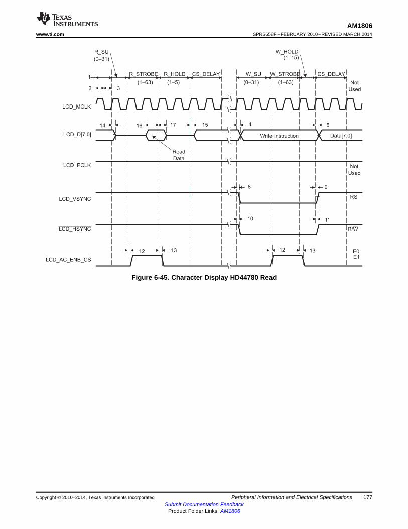
LCD_AC_ENB_CS
LCD_PCLK
LCD_VSYNC
LCD_HSYNC
R_SU
R_STROBE R_HOLD
(0–31)
(1–63) (1–5)
CS_DELAY
Not
Used
RS
R/W
LCD_MCLK
1
2 3
W_SU W_STROBE
W_HOLD
(0–31) (1–63)
(1–15)
CS_DELAY
8 9
12 13
10 11
Not
Used
LCD_D[7:0]
14 1716
Read
Data
15 4 5
E0E1
12 13
Data[7:0]Write Instruction
AM1806www.ti.com SPRS658F –FEBRUARY 2010–REVISED MARCH 2014
Figure 6-45. Character Display HD44780 Read
Copyright © 2010–2014, Texas Instruments Incorporated Peripheral Information and Electrical Specifications 177Submit Documentation Feedback
Product Folder Links: AM1806
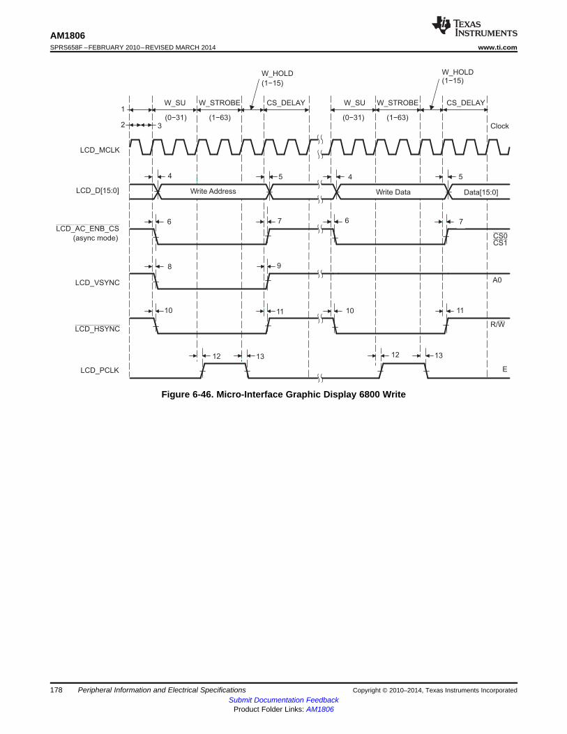
LCD_D[15:0]
LCD_AC_ENB_CS
(async mode)
LCD_VSYNC
LCD_HSYNC
LCD_MCLK
LCD_PCLK
4
W_SU W_STROBE
W_HOLD
(0−31) (1−63)
(1−15)
CS_DELAY
CS0CS1
A0
R/W
E
Clock
1
2 3
W_SU W_STROBE
W_HOLD
(0−31) (1−63)
(1−15)
CS_DELAY
5 4 5
6 7 6 7
8 9
12 13
Write Address Write Data
12 13
10 11 10 11
Data[15:0]
AM1806SPRS658F –FEBRUARY 2010–REVISED MARCH 2014 www.ti.com
Figure 6-46. Micro-Interface Graphic Display 6800 Write
178 Peripheral Information and Electrical Specifications Copyright © 2010–2014, Texas Instruments IncorporatedSubmit Documentation Feedback
Product Folder Links: AM1806
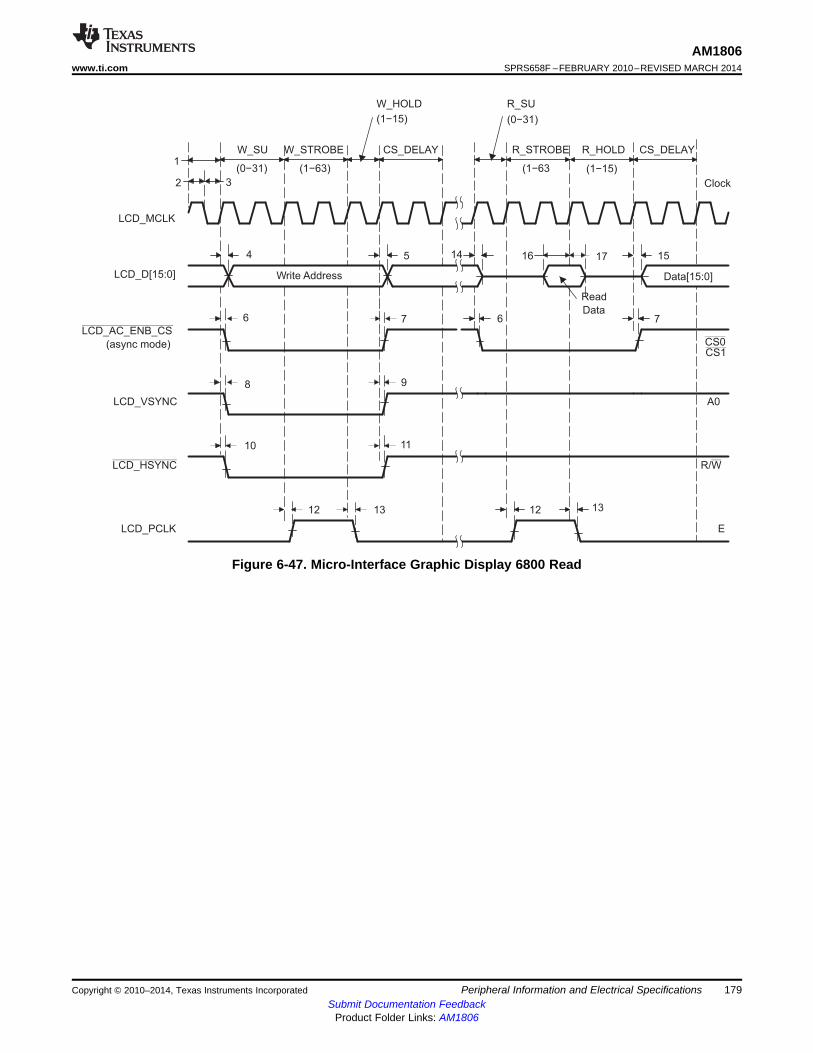
LCD_D[15:0]
LCD_AC_ENB_CS
(async mode)
LCD_VSYNC
LCD_HSYNC
LCD_MCLK
LCD_PCLK
4
W_SU W_STROBE
W_HOLD
(0−31) (1−63)
(1−15)
CS_DELAY
CS0CS1
A0
R/W
E
Clock
1
2 3
R_SU
R_STROBE R_HOLD
(0−31)
(1−63 (1−15)
CS_DELAY
5 14 15
6 7 6 7
8 9
12 13
1716
Write Address
Read
Data
10 11
1213
Data[15:0]
AM1806www.ti.com SPRS658F –FEBRUARY 2010–REVISED MARCH 2014
Figure 6-47. Micro-Interface Graphic Display 6800 Read
Copyright © 2010–2014, Texas Instruments Incorporated Peripheral Information and Electrical Specifications 179Submit Documentation Feedback
Product Folder Links: AM1806
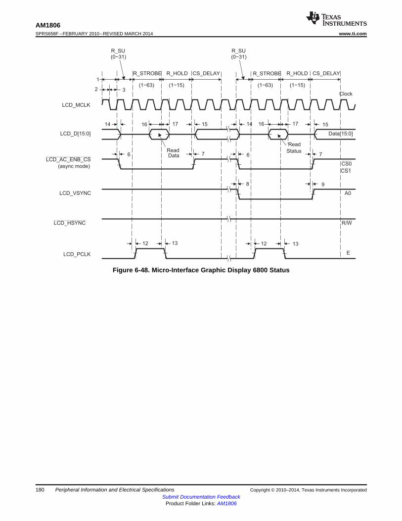
ReadData
LCD_D[15:0]
LCD_AC_ENB_CS
(async mode)
LCD_VSYNC
LCD_HSYNC
LCD_MCLK
LCD_PCLK
R_SU
R_STROBE R_HOLD
(0−31)
(1−63) (1−15)
CS_DELAY
CS0
CS1
A0
R/W
E
Clock
1
2 3
R_STROBE R_HOLD
(1−63) (1−15)
CS_DELAY
14 15
6 7 6 7
8 9
12 13
171614 1716 15
12 13
Data[15:0]
R_SU(0−31)
Read
Status
AM1806SPRS658F –FEBRUARY 2010–REVISED MARCH 2014 www.ti.com
Figure 6-48. Micro-Interface Graphic Display 6800 Status
180 Peripheral Information and Electrical Specifications Copyright © 2010–2014, Texas Instruments IncorporatedSubmit Documentation Feedback
Product Folder Links: AM1806
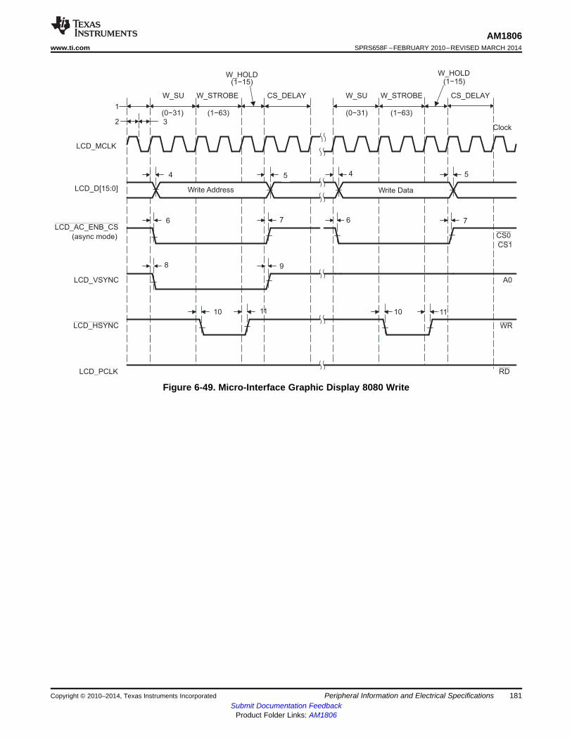
LCD_D[15:0]
LCD_AC_ENB_CS
(async mode)
LCD_VSYNC
LCD_HSYNC
LCD_MCLK
LCD_PCLK
4
W_SU W_STROBE
W_HOLD
(0−31) (1−63)
(1−15)
CS_DELAY
DATA[15:0]
CS0
CS1
A0
WR
RD
Clock
1
2 3
W_SU W_STROBE
W_HOLD
(0−31) (1−63)
(1−15)
CS_DELAY
5 4 5
6 7 6 7
8 9
10 11
Write Address Write Data
10 11
AM1806www.ti.com SPRS658F –FEBRUARY 2010–REVISED MARCH 2014
Figure 6-49. Micro-Interface Graphic Display 8080 Write
Copyright © 2010–2014, Texas Instruments Incorporated Peripheral Information and Electrical Specifications 181Submit Documentation Feedback
Product Folder Links: AM1806
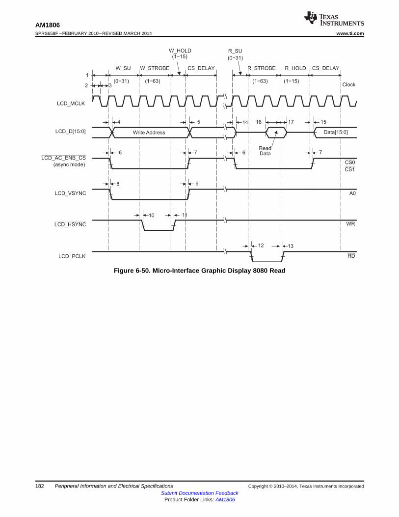
LCD_D[15:0]
LCD_AC_ENB_CS
(async mode)
LCD_VSYNC
LCD_HSYNC
LCD_MCLK
LCD_PCLK
4
W_SU W_STROBE
W_HOLD
(0−31) (1−63)
(1−15)
CS_DELAY
CS0
CS1
A0
WR
RD
Clock
1
2 3
R_SU
R_STROBE R_HOLD
(0−31)
(1−63) (1−15)
CS_DELAY
5 14 15
6 7 6 7
8 9
12 13
1716
ReadData
10 11
Data[15:0]Write Address
AM1806SPRS658F –FEBRUARY 2010–REVISED MARCH 2014 www.ti.com
Figure 6-50. Micro-Interface Graphic Display 8080 Read
182 Peripheral Information and Electrical Specifications Copyright © 2010–2014, Texas Instruments IncorporatedSubmit Documentation Feedback
Product Folder Links: AM1806

LCD_D[15:0]
LCD_AC_ENB_CS
LCD_VSYNC
LCD_HSYNC
LCD_MCLK
LCD_PCLK
R_SU
R_STROBE R_HOLD
(0−31)
(1−63) (1−15)
CS_DELAY
CS0
CS1
A0
WR
RD
Clock
1
23
R_STROBE R_HOLD
(1−63) (1−15)
CS_DELAY
14 15
6 7 6
8
12 13
1716
Read Status
14 1716
Read Data
15
12 13
Data[15:0]
7
9
R_SU(0−31)
AM1806www.ti.com SPRS658F –FEBRUARY 2010–REVISED MARCH 2014
Figure 6-51. Micro-Interface Graphic Display 8080 Status
Copyright © 2010–2014, Texas Instruments Incorporated Peripheral Information and Electrical Specifications 183Submit Documentation Feedback
Product Folder Links: AM1806
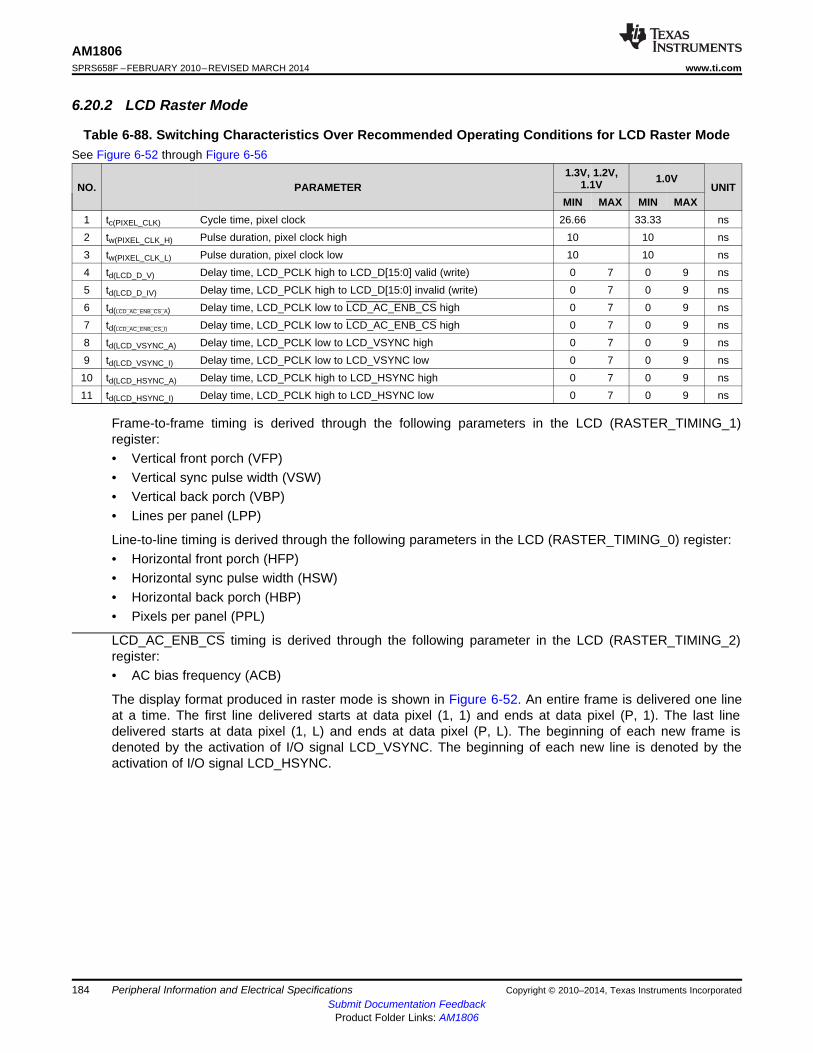
AM1806SPRS658F –FEBRUARY 2010–REVISED MARCH 2014 www.ti.com
6.20.2 LCD Raster Mode
Table 6-88. Switching Characteristics Over Recommended Operating Conditions for LCD Raster ModeSee Figure 6-52 through Figure 6-56
1.3V, 1.2V, 1.0V1.1VNO. PARAMETER UNITMIN MAX MIN MAX
1 tc(PIXEL_CLK) Cycle time, pixel clock 26.66 33.33 ns2 tw(PIXEL_CLK_H) Pulse duration, pixel clock high 10 10 ns3 tw(PIXEL_CLK_L) Pulse duration, pixel clock low 10 10 ns4 td(LCD_D_V) Delay time, LCD_PCLK high to LCD_D[15:0] valid (write) 0 7 0 9 ns5 td(LCD_D_IV) Delay time, LCD_PCLK high to LCD_D[15:0] invalid (write) 0 7 0 9 ns6 td(LCD_AC_ENB_CS_A) Delay time, LCD_PCLK low to LCD_AC_ENB_CS high 0 7 0 9 ns7 td(LCD_AC_ENB_CS_I) Delay time, LCD_PCLK low to LCD_AC_ENB_CS high 0 7 0 9 ns8 td(LCD_VSYNC_A) Delay time, LCD_PCLK low to LCD_VSYNC high 0 7 0 9 ns9 td(LCD_VSYNC_I) Delay time, LCD_PCLK low to LCD_VSYNC low 0 7 0 9 ns10 td(LCD_HSYNC_A) Delay time, LCD_PCLK high to LCD_HSYNC high 0 7 0 9 ns11 td(LCD_HSYNC_I) Delay time, LCD_PCLK high to LCD_HSYNC low 0 7 0 9 ns
Frame-to-frame timing is derived through the following parameters in the LCD (RASTER_TIMING_1)register:• Vertical front porch (VFP)• Vertical sync pulse width (VSW)• Vertical back porch (VBP)• Lines per panel (LPP)
Line-to-line timing is derived through the following parameters in the LCD (RASTER_TIMING_0) register:• Horizontal front porch (HFP)• Horizontal sync pulse width (HSW)• Horizontal back porch (HBP)• Pixels per panel (PPL)
LCD_AC_ENB_CS timing is derived through the following parameter in the LCD (RASTER_TIMING_2)register:• AC bias frequency (ACB)
The display format produced in raster mode is shown in Figure 6-52. An entire frame is delivered one lineat a time. The first line delivered starts at data pixel (1, 1) and ends at data pixel (P, 1). The last linedelivered starts at data pixel (1, L) and ends at data pixel (P, L). The beginning of each new frame isdenoted by the activation of I/O signal LCD_VSYNC. The beginning of each new line is denoted by theactivation of I/O signal LCD_HSYNC.
184 Peripheral Information and Electrical Specifications Copyright © 2010–2014, Texas Instruments IncorporatedSubmit Documentation Feedback
Product Folder Links: AM1806
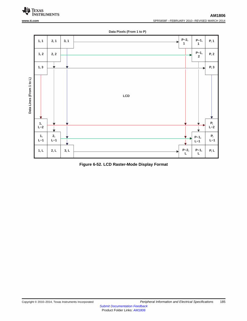
LCD
1, 1 2, 1 3, 1
1, 2 2, 2
1, 3
P, 1P−1,1
P−2,
P, 2P−1,2
P, 3
1, L
1,L−1
1,L−2
3, L2, L
2,L−1
P, L
P−1,L−1
P,L−1
P−1,L
P,L−2
P−2,L
Data Pixels (From 1 to P)D
ata
Line
s (F
rom
1 to
L)
1
AM1806www.ti.com SPRS658F –FEBRUARY 2010–REVISED MARCH 2014
Figure 6-52. LCD Raster-Mode Display Format
Copyright © 2010–2014, Texas Instruments Incorporated Peripheral Information and Electrical Specifications 185Submit Documentation Feedback
Product Folder Links: AM1806
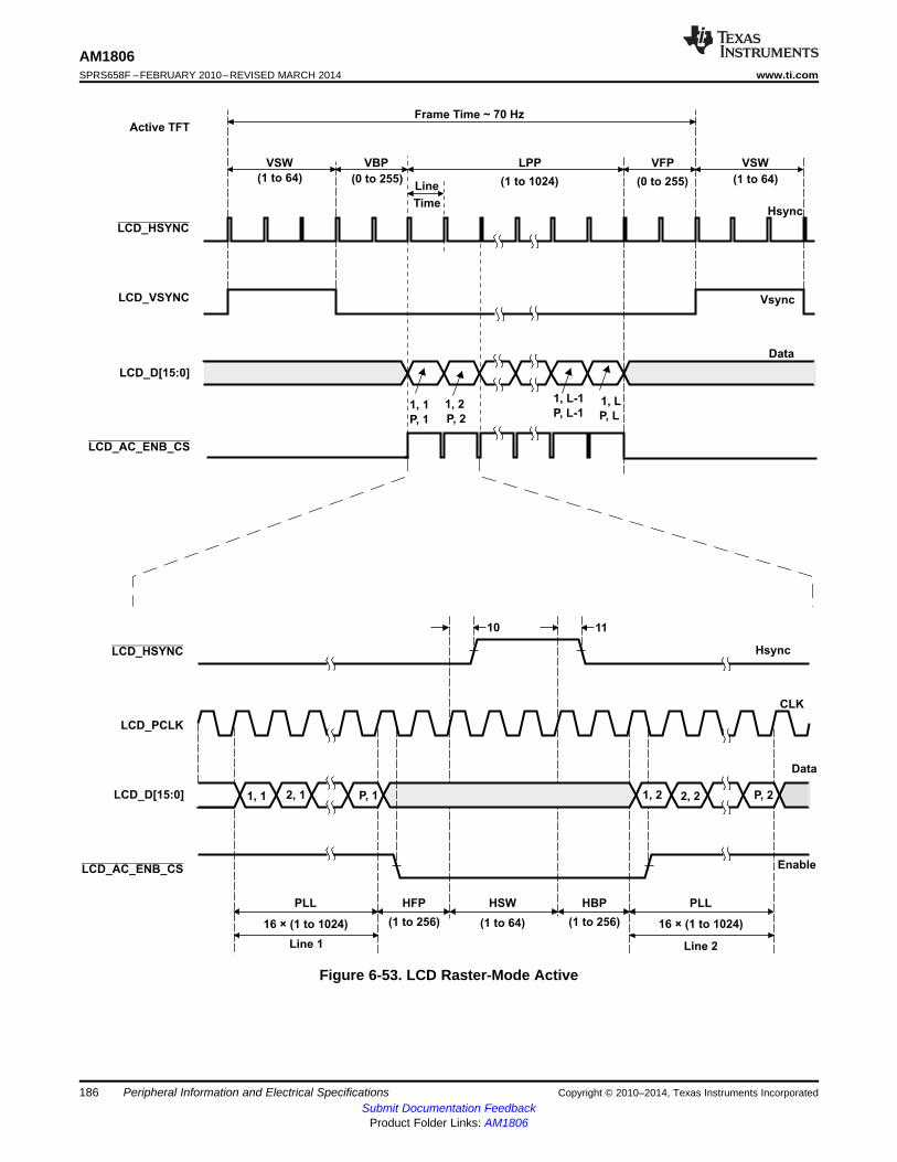
LCD_HSYNC
Hsync
LCD_VSYNC
(1 to 64)
VSW
(1 to 64)
VSW
(0 to 255)
VFP
(1 to 1024)
Frame Time 70 Hz~
LPP
(0 to 255)
LCD_D[15:0]
1, 1
P, 1
1, 2
P, 2
1, L
P, L
1, L-1
P, L-1
Line
Time
Vsync
Data
Active TFT
LCD_AC_ENB_CS
VBP
CLK
LCD_HSYNC Hsync
10 11
LCD_PCLK
LCD_D[15:0] 1, 1 2, 2 P, 2P, 12, 1 1, 2
PLL
16 × (1 to 1024)
HBP
(1 to 256)
Line 1
(1 to 256)
HFP
(1 to 64)
HSW PLL
16 × (1 to 1024)
Line 2
Data
LCD_AC_ENB_CS Enable
AM1806SPRS658F –FEBRUARY 2010–REVISED MARCH 2014 www.ti.com
Figure 6-53. LCD Raster-Mode Active
186 Peripheral Information and Electrical Specifications Copyright © 2010–2014, Texas Instruments IncorporatedSubmit Documentation Feedback
Product Folder Links: AM1806
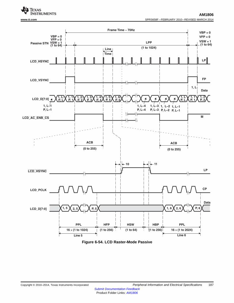
AM1806www.ti.com SPRS658F –FEBRUARY 2010–REVISED MARCH 2014
Figure 6-54. LCD Raster-Mode Passive
Copyright © 2010–2014, Texas Instruments Incorporated Peripheral Information and Electrical Specifications 187Submit Documentation Feedback
Product Folder Links: AM1806
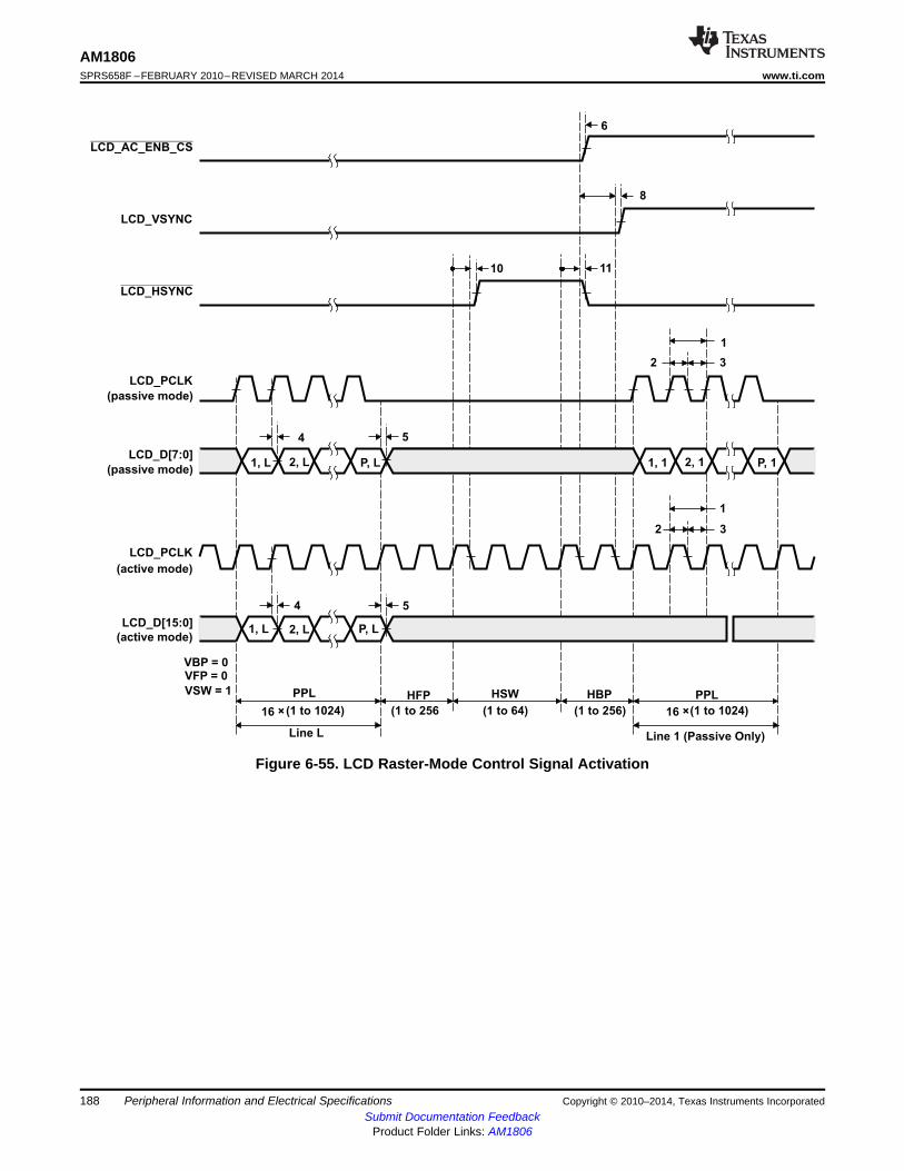
LCD_HSYNC
LCD_PCLK
(active mode)
LCD_D[15:0]
(active mode)1, L P, L2, L
PPL
16 ×(1 to 1024)
HBP
(1 to 256
Line L
(1 to 256)
HFP
(1 to 64)
HSW PPL
16 ×(1 to 1024)
Line 1 (Passive Only)
LCD_VSYNC
LCD_PCLK
(passive mode)
LCD_AC_ENB_CS
LCD_D[7:0]
(passive mode)1, L 2, 1 P, 1P, L2, L 1, 1
10 11
8
6
4
4
5
5
1
2 3
1
2 3
VSW = 1
VFP = 0VBP = 0
AM1806SPRS658F –FEBRUARY 2010–REVISED MARCH 2014 www.ti.com
Figure 6-55. LCD Raster-Mode Control Signal Activation
188 Peripheral Information and Electrical Specifications Copyright © 2010–2014, Texas Instruments IncorporatedSubmit Documentation Feedback
Product Folder Links: AM1806
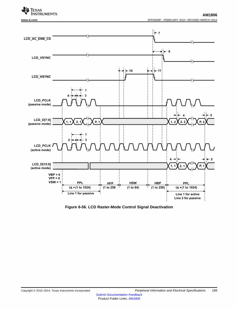
LCD_HSYNC
LCD_PCLK
(active mode)
LCD_D[15:0]
(active mode)
PPL
16 ×(1 to 1024)
HBP
(1 to 256
Line 1 for passive
(1 to 256)
HFP
(1 to 64)
HSW PPL
16 ×(1 to 1024)
Line 1 for active
LCD_VSYNC
LCD_PCLK
(passive mode)
LCD_AC_ENB_CS
LCD_D[7:0]
(passive mode)1, 1 2, 2 P, 2P, 12, 1 1, 2
10 11
9
7
4 5
1
2 3
VSW = 1
VFP = 0VBP = 0
P, 11, 1 2, 1
4 5
1
34
Line 2 for passive
AM1806www.ti.com SPRS658F –FEBRUARY 2010–REVISED MARCH 2014
Figure 6-56. LCD Raster-Mode Control Signal Deactivation
Copyright © 2010–2014, Texas Instruments Incorporated Peripheral Information and Electrical Specifications 189Submit Documentation Feedback
Product Folder Links: AM1806
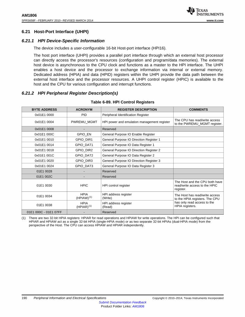
AM1806SPRS658F –FEBRUARY 2010–REVISED MARCH 2014 www.ti.com
6.21 Host-Port Interface (UHPI)
6.21.1 HPI Device-Specific InformationThe device includes a user-configurable 16-bit Host-port interface (HPI16).
The host port interface (UHPI) provides a parallel port interface through which an external host processorcan directly access the processor's resources (configuration and program/data memories). The externalhost device is asynchronous to the CPU clock and functions as a master to the HPI interface. The UHPIenables a host device and the processor to exchange information via internal or external memory.Dedicated address (HPIA) and data (HPID) registers within the UHPI provide the data path between theexternal host interface and the processor resources. A UHPI control register (HPIC) is available to thehost and the CPU for various configuration and interrupt functions.
6.21.2 HPI Peripheral Register Description(s)
Table 6-89. HPI Control Registers
BYTE ADDRESS ACRONYM REGISTER DESCRIPTION COMMENTS0x01E1 0000 PID Peripheral Identification Register
The CPU has read/write access0x01E1 0004 PWREMU_MGMT HPI power and emulation management register to the PWREMU_MGMT register.0x01E1 0008 - Reserved0x01E1 000C GPIO_EN General Purpose IO Enable Register0x01E1 0010 GPIO_DIR1 General Purpose IO Direction Register 10x01E1 0014 GPIO_DAT1 General Purpose IO Data Register 10x01E1 0018 GPIO_DIR2 General Purpose IO Direction Register 20x01E1 001C GPIO_DAT2 General Purpose IO Data Register 20x01E1 0020 GPIO_DIR3 General Purpose IO Direction Register 30x01E1 0024 GPIO_DAT3 General Purpose IO Data Register 301E1 0028 - Reserved01E1 002C - Reserved
The Host and the CPU both have01E1 0030 HPIC HPI control register read/write access to the HPIC
register.HPIA HPI address register The Host has read/write access01E1 0034 (HPIAW) (1) (Write) to the HPIA registers. The CPU
has only read access to theHPIA HPI address register01E1 0038 HPIA registers.(HPIAR) (1) (Read)01E1 000C - 01E1 07FF - Reserved
(1) There are two 32-bit HPIA registers: HPIAR for read operations and HPIAW for write operations. The HPI can be configured such thatHPIAR and HPIAW act as a single 32-bit HPIA (single-HPIA mode) or as two separate 32-bit HPIAs (dual-HPIA mode) from theperspective of the Host. The CPU can access HPIAW and HPIAR independently.
190 Peripheral Information and Electrical Specifications Copyright © 2010–2014, Texas Instruments IncorporatedSubmit Documentation Feedback
Product Folder Links: AM1806
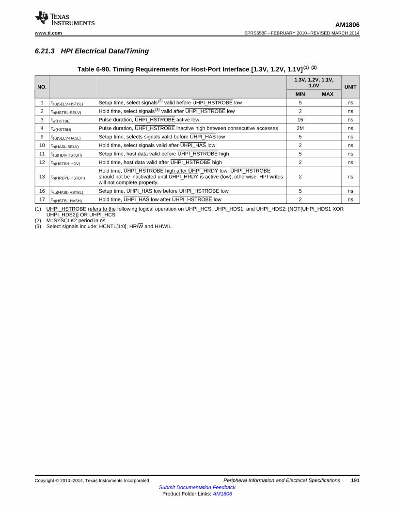
AM1806www.ti.com SPRS658F –FEBRUARY 2010–REVISED MARCH 2014
6.21.3 HPI Electrical Data/Timing
Table 6-90. Timing Requirements for Host-Port Interface [1.3V, 1.2V, 1.1V] (1) (2)
1.3V, 1.2V, 1.1V,1.0VNO. UNIT
MIN MAX1 tsu(SELV-HSTBL) Setup time, select signals (3) valid before UHPI_HSTROBE low 5 ns2 th(HSTBL-SELV) Hold time, select signals (3) valid after UHPI_HSTROBE low 2 ns3 tw(HSTBL) Pulse duration, UHPI_HSTROBE active low 15 ns4 tw(HSTBH) Pulse duration, UHPI_HSTROBE inactive high between consecutive accesses 2M ns9 tsu(SELV-HASL) Setup time, selects signals valid before UHPI_HAS low 5 ns10 th(HASL-SELV) Hold time, select signals valid after UHPI_HAS low 2 ns11 tsu(HDV-HSTBH) Setup time, host data valid before UHPI_HSTROBE high 5 ns12 th(HSTBH-HDV) Hold time, host data valid after UHPI_HSTROBE high 2 ns
Hold time, UHPI_HSTROBE high after UHPI_HRDY low. UHPI_HSTROBE13 th(HRDYL-HSTBH) should not be inactivated until UHPI_HRDY is active (low); otherwise, HPI writes 2 ns
will not complete properly.16 tsu(HASL-HSTBL) Setup time, UHPI_HAS low before UHPI_HSTROBE low 5 ns17 th(HSTBL-HASH) Hold time, UHPI_HAS low after UHPI_HSTROBE low 2 ns
(1) UHPI_HSTROBE refers to the following logical operation on UHPI_HCS, UHPI_HDS1, and UHPI_HDS2: [NOT(UHPI_HDS1 XORUHPI_HDS2)] OR UHPI_HCS.
(2) M=SYSCLK2 period in ns.(3) Select signals include: HCNTL[1:0], HR/W and HHWIL.
Copyright © 2010–2014, Texas Instruments Incorporated Peripheral Information and Electrical Specifications 191Submit Documentation Feedback
Product Folder Links: AM1806
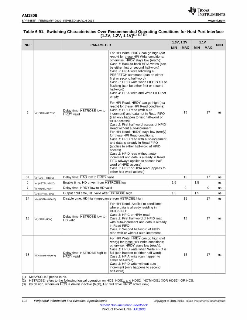
AM1806SPRS658F –FEBRUARY 2010–REVISED MARCH 2014 www.ti.com
Table 6-91. Switching Characteristics Over Recommended Operating Conditions for Host-Port Interface[1.3V, 1.2V, 1.1V] (1) (2) (3)
1.3V, 1.2V 1.1VNO. PARAMETER UNIT
MIN MAX MIN MAXFor HPI Write, HRDY can go high (notready) for these HPI Write conditions;otherwise, HRDY stays low (ready):Case 1: Back-to-back HPIA writes (canbe either first or second half-word)Case 2: HPIA write following aPREFETCH command (can be eitherfirst or second half-word)Case 3: HPID write when FIFO is full orflushing (can be either first or secondhalf-word)Case 4: HPIA write and Write FIFO notempty
For HPI Read, HRDY can go high (notready) for these HPI Read conditions:Case 1: HPID read (with auto-Delay time, HSTROBE low to5 td(HSTBL-HRDYV) 15 17 nsincrement) and data not in Read FIFOHRDY valid(can only happen to first half-word ofHPID access)Case 2: First half-word access of HPIDRead without auto-incrementFor HPI Read, HRDY stays low (ready)for these HPI Read conditions:Case 1: HPID read with auto-incrementand data is already in Read FIFO(applies to either half-word of HPIDaccess)Case 2: HPID read without auto-increment and data is already in ReadFIFO (always applies to second half-word of HPID access)Case 3: HPIC or HPIA read (applies toeither half-word access)
5a td(HASL-HRDYV) Delay time, HAS low to HRDY valid 15 17 ns6 ten(HSTBL-HDLZ) Enable time, HD driven from HSTROBE low 1.5 1.5 ns7 td(HRDYL-HDV) Delay time, HRDY low to HD valid 0 0 ns8 toh(HSTBH-HDV) Output hold time, HD valid after HSTROBE high 1.5 1.5 ns14 tdis(HSTBH-HDHZ) Disable time, HD high-impedance from HSTROBE high 15 17 ns
For HPI Read. Applies to conditionswhere data is already residing inHPID/FIFO:Case 1: HPIC or HPIA readDelay time, HSTROBE low to15 td(HSTBL-HDV) Case 2: First half-word of HPID read 15 17 nsHD valid with auto-increment and data is alreadyin Read FIFOCase 3: Second half-word of HPIDread with or without auto-incrementFor HPI Write, HRDY can go high (notready) for these HPI Write conditions;otherwise, HRDY stays low (ready):Case 1: HPID write when Write FIFO is
Delay time, HSTROBE high to full (can happen to either half-word)18 td(HSTBH-HRDYV) 15 17 nsHRDY valid Case 2: HPIA write (can happen toeither half-word)Case 3: HPID write without auto-increment (only happens to secondhalf-word)
(1) M=SYSCLK2 period in ns.(2) HSTROBE refers to the following logical operation on HCS, HDS1, and HDS2: [NOT(HDS1 XOR HDS2)] OR HCS.(3) By design, whenever HCS is driven inactive (high), HPI will drive HRDY active (low).
192 Peripheral Information and Electrical Specifications Copyright © 2010–2014, Texas Instruments IncorporatedSubmit Documentation Feedback
Product Folder Links: AM1806
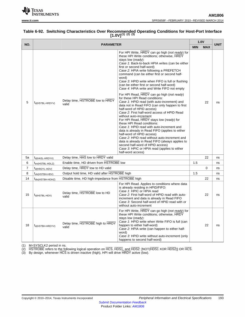
AM1806www.ti.com SPRS658F –FEBRUARY 2010–REVISED MARCH 2014
Table 6-92. Switching Characteristics Over Recommended Operating Conditions for Host-Port Interface[1.0V] (1) (2) (3)
1.0VNO. PARAMETER UNIT
MIN MAXFor HPI Write, HRDY can go high (not ready) forthese HPI Write conditions; otherwise, HRDYstays low (ready):Case 1: Back-to-back HPIA writes (can be eitherfirst or second half-word)Case 2: HPIA write following a PREFETCHcommand (can be either first or second half-word)Case 3: HPID write when FIFO is full or flushing(can be either first or second half-word)Case 4: HPIA write and Write FIFO not empty
For HPI Read, HRDY can go high (not ready)for these HPI Read conditions:
Delay time, HSTROBE low to HRDY Case 1: HPID read (with auto-increment) and5 td(HSTBL-HRDYV) 22 nsvalid data not in Read FIFO (can only happen to firsthalf-word of HPID access)Case 2: First half-word access of HPID Readwithout auto-incrementFor HPI Read, HRDY stays low (ready) forthese HPI Read conditions:Case 1: HPID read with auto-increment anddata is already in Read FIFO (applies to eitherhalf-word of HPID access)Case 2: HPID read without auto-increment anddata is already in Read FIFO (always applies tosecond half-word of HPID access)Case 3: HPIC or HPIA read (applies to eitherhalf-word access)
5a td(HASL-HRDYV) Delay time, HAS low to HRDY valid 22 ns6 ten(HSTBL-HDLZ) Enable time, HD driven from HSTROBE low 1.5 ns7 td(HRDYL-HDV) Delay time, HRDY low to HD valid 0 ns8 toh(HSTBH-HDV) Output hold time, HD valid after HSTROBE high 1.5 ns14 tdis(HSTBH-HDHZ) Disable time, HD high-impedance from HSTROBE high 22 ns
For HPI Read. Applies to conditions where datais already residing in HPID/FIFO:Case 1: HPIC or HPIA readDelay time, HSTROBE low to HD15 td(HSTBL-HDV) Case 2: First half-word of HPID read with auto- 22 nsvalid increment and data is already in Read FIFOCase 3: Second half-word of HPID read with orwithout auto-incrementFor HPI Write, HRDY can go high (not ready) forthese HPI Write conditions; otherwise, HRDYstays low (ready):Case 1: HPID write when Write FIFO is full (canDelay time, HSTROBE high to HRDY18 td(HSTBH-HRDYV) happen to either half-word) 22 nsvalid Case 2: HPIA write (can happen to either half-word)Case 3: HPID write without auto-increment (onlyhappens to second half-word)
(1) M=SYSCLK2 period in ns.(2) HSTROBE refers to the following logical operation on HCS, HDS1, and HDS2: [NOT(HDS1 XOR HDS2)] OR HCS.(3) By design, whenever HCS is driven inactive (high), HPI will drive HRDY active (low).
Copyright © 2010–2014, Texas Instruments Incorporated Peripheral Information and Electrical Specifications 193Submit Documentation Feedback
Product Folder Links: AM1806
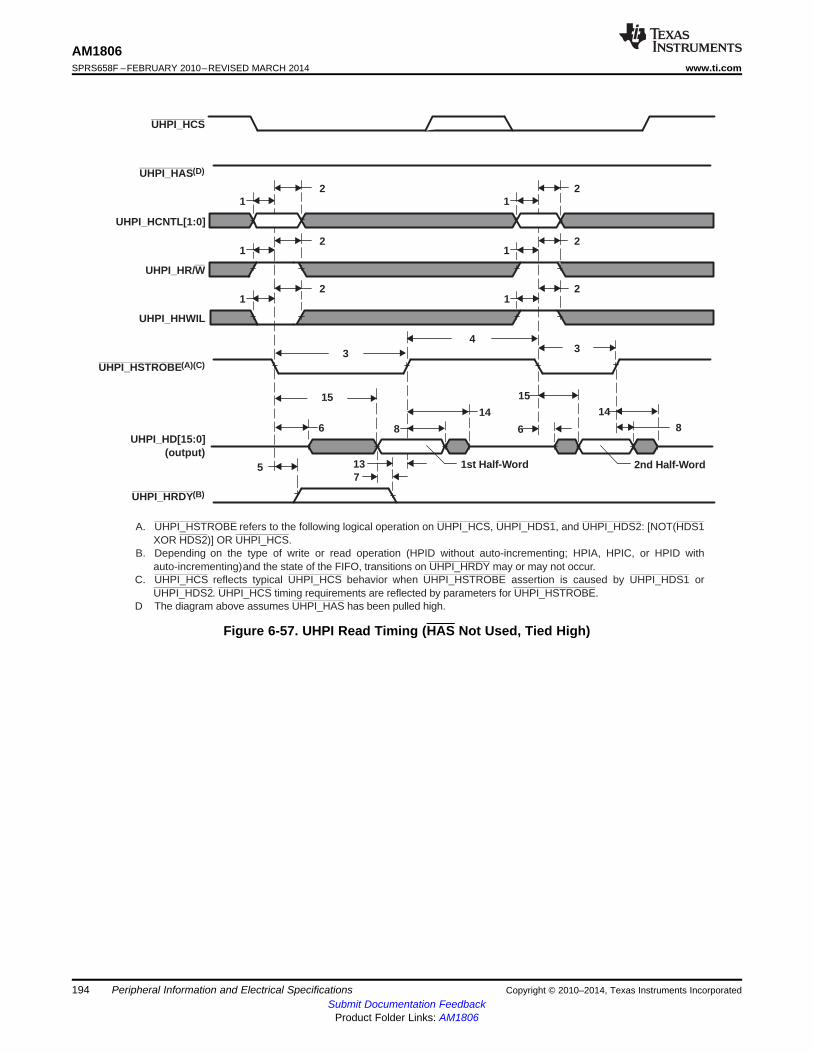
UHPI_HCS
UHPI_HAS(D)
UHPI_HCNTL[1:0]
UHPI_HR/W
UHPI_HHWIL
UHPI_HSTROBE(A)(C)
UHPI_HD[15:0](output)
UHPI_HRDY(B)
12
12
12
5
6
34
3
12
12
12
8
14
15
14
8
71st Half-W ord 2nd Half-W ord
6
13
15
A. UHPI_HSTROBE refers to the following logical operation on UHPI_HCS, UHPI_HDS1, and UHPI_HDS2: [NOT(HDS1XOR HDS2)] OR UHPI_HCS.
B. Depending on the type of write or read operation (HPID without auto-incrementing; HPIA, HPIC, or HPID withauto-incrementing) and the state of the FIFO, transitions on UHPI_HRDY may or may not occur.
C. UHPI_HCS reflects typical UHPI_HCS behavior when UHPI_HSTROBE assertion is caused by UHPI_HDS1 orUHPI_HDS2. UHPI_HCS timing requirements are reflected by parameters for UHPI_HSTROBE.
D The diagram above assumes UHPI_HAS has been pulled high.
AM1806SPRS658F –FEBRUARY 2010–REVISED MARCH 2014 www.ti.com
Figure 6-57. UHPI Read Timing (HAS Not Used, Tied High)
194 Peripheral Information and Electrical Specifications Copyright © 2010–2014, Texas Instruments IncorporatedSubmit Documentation Feedback
Product Folder Links: AM1806
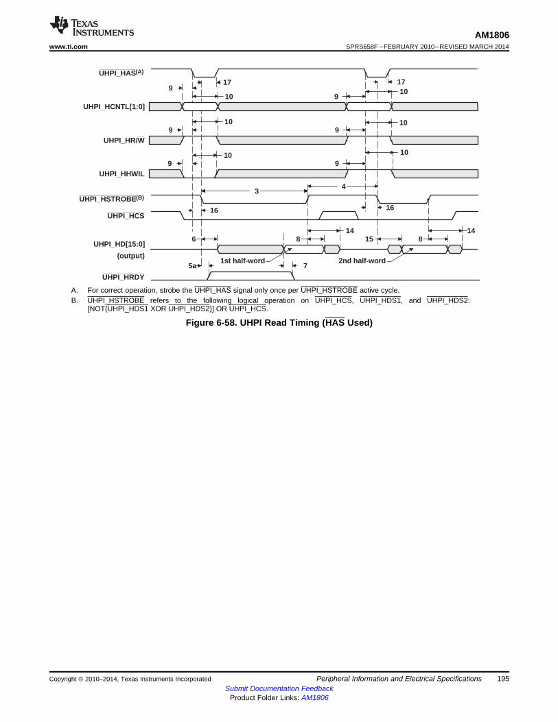
UHPI_HAS(A)
UHPI_HCNTL[1:0]
UHPI_HR/W
UHPI_HHWIL
UHPI_HSTROBE(B)
UHPI_HCS
UHPI_HD[15:0]
(output)
UHPI_HRDY
1st half-word 2nd half-word75a
14815
1486
43
10
910
9
109
109
10910
917 17
1616
AM1806www.ti.com SPRS658F –FEBRUARY 2010–REVISED MARCH 2014
A. For correct operation, strobe the UHPI_HAS signal only once per UHPI_HSTROBE active cycle.B. UHPI_HSTROBE refers to the following logical operation on UHPI_HCS, UHPI_HDS1, and UHPI_HDS2:
[NOT(UHPI_HDS1 XOR UHPI_HDS2)] OR UHPI_HCS.
Figure 6-58. UHPI Read Timing (HAS Used)
Copyright © 2010–2014, Texas Instruments Incorporated Peripheral Information and Electrical Specifications 195Submit Documentation Feedback
Product Folder Links: AM1806
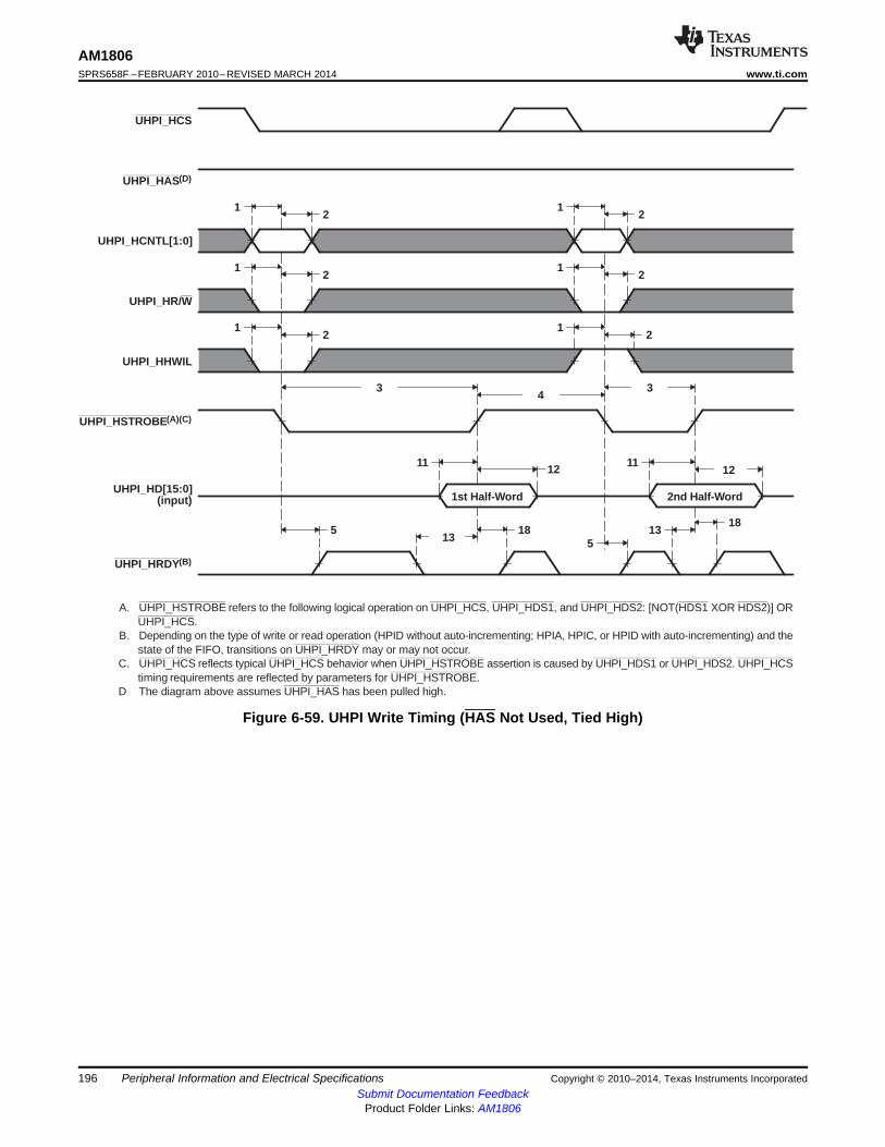
UHPI_HAS(D)
UHPI_HCNTL[1:0]
UHPI_HR/W
UHPI_HHWIL
UHPI_HSTROBE(A)(C)
UHPI_HCS
UHPI_HD[15:0](input)
UHPI_HRDY(B)
21
21
12
21
21
12
34
3
1112
1813
5185
1112
13
2nd Half-W ord1st Half-W ord
A. UHPI_HSTROBE refers to the following logical operation on UHPI_HCS, UHPI_HDS1, and UHPI_HDS2: [NOT(HDS1 XOR HDS2)] ORUHPI_HCS.
B. Depending on the type of write or read operation (HPID without auto-incrementing; HPIA, HPIC, or HPID with auto-incrementing) and thestate of the FIFO, transitions on UHPI_HRDY may or may not occur.
C. UHPI_HCS reflects typical UHPI_HCS behavior when UHPI_HSTROBE assertion is caused by UHPI_HDS1 or UHPI_HDS2. UHPI_HCStiming requirements are reflected by parameters for UHPI_HSTROBE.
D The diagram above assumes UHPI_HAS has been pulled high.
AM1806SPRS658F –FEBRUARY 2010–REVISED MARCH 2014 www.ti.com
Figure 6-59. UHPI Write Timing (HAS Not Used, Tied High)
196 Peripheral Information and Electrical Specifications Copyright © 2010–2014, Texas Instruments IncorporatedSubmit Documentation Feedback
Product Folder Links: AM1806
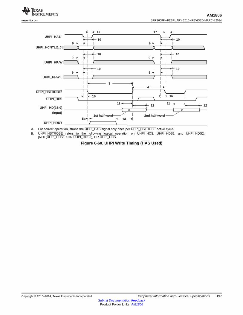
1st half-word 2nd half-word
1211
1211
4
13
3
109
109
109
109
109
109
UHPI_HAS†
UHPI_HCNTL[1:0]
UHPI_HR/W
UHPI_HHWIL
UHPI_HSTROBE‡
UHPI_HCS
UHPI_HD[15:0]
(input)
UHPI_HRDY
1717
16 16
5a
AM1806www.ti.com SPRS658F –FEBRUARY 2010–REVISED MARCH 2014
A. For correct operation, strobe the UHPI_HAS signal only once per UHPI_HSTROBE active cycle.B. UHPI_HSTROBE refers to the following logical operation on UHPI_HCS, UHPI_HDS1, and UHPI_HDS2:
[NOT(UHPI_HDS1 XOR UHPI_HDS2)] OR UHPI_HCS.
Figure 6-60. UHPI Write Timing (HAS Used)
Copyright © 2010–2014, Texas Instruments Incorporated Peripheral Information and Electrical Specifications 197Submit Documentation Feedback
Product Folder Links: AM1806
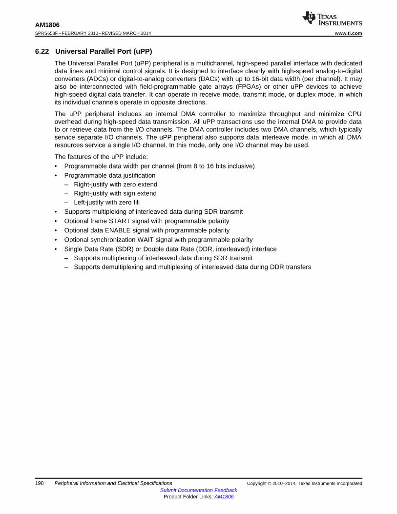
AM1806SPRS658F –FEBRUARY 2010–REVISED MARCH 2014 www.ti.com
6.22 Universal Parallel Port (uPP)The Universal Parallel Port (uPP) peripheral is a multichannel, high-speed parallel interface with dedicateddata lines and minimal control signals. It is designed to interface cleanly with high-speed analog-to-digitalconverters (ADCs) or digital-to-analog converters (DACs) with up to 16-bit data width (per channel). It mayalso be interconnected with field-programmable gate arrays (FPGAs) or other uPP devices to achievehigh-speed digital data transfer. It can operate in receive mode, transmit mode, or duplex mode, in whichits individual channels operate in opposite directions.
The uPP peripheral includes an internal DMA controller to maximize throughput and minimize CPUoverhead during high-speed data transmission. All uPP transactions use the internal DMA to provide datato or retrieve data from the I/O channels. The DMA controller includes two DMA channels, which typicallyservice separate I/O channels. The uPP peripheral also supports data interleave mode, in which all DMAresources service a single I/O channel. In this mode, only one I/O channel may be used.
The features of the uPP include:• Programmable data width per channel (from 8 to 16 bits inclusive)• Programmable data justification
– Right-justify with zero extend– Right-justify with sign extend– Left-justify with zero fill
• Supports multiplexing of interleaved data during SDR transmit• Optional frame START signal with programmable polarity• Optional data ENABLE signal with programmable polarity• Optional synchronization WAIT signal with programmable polarity• Single Data Rate (SDR) or Double data Rate (DDR, interleaved) interface
– Supports multiplexing of interleaved data during SDR transmit– Supports demultiplexing and multiplexing of interleaved data during DDR transfers
198 Peripheral Information and Electrical Specifications Copyright © 2010–2014, Texas Instruments IncorporatedSubmit Documentation Feedback
Product Folder Links: AM1806
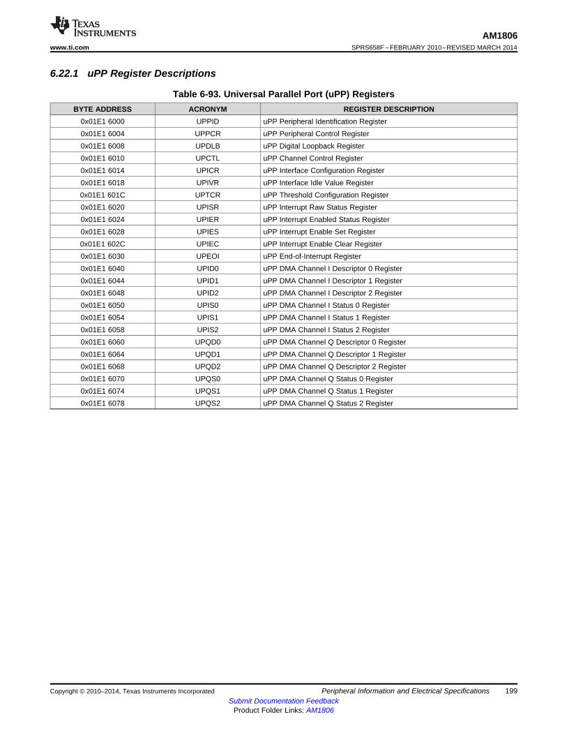
AM1806www.ti.com SPRS658F –FEBRUARY 2010–REVISED MARCH 2014
6.22.1 uPP Register Descriptions
Table 6-93. Universal Parallel Port (uPP) RegistersBYTE ADDRESS ACRONYM REGISTER DESCRIPTION
0x01E1 6000 UPPID uPP Peripheral Identification Register0x01E1 6004 UPPCR uPP Peripheral Control Register0x01E1 6008 UPDLB uPP Digital Loopback Register0x01E1 6010 UPCTL uPP Channel Control Register0x01E1 6014 UPICR uPP Interface Configuration Register0x01E1 6018 UPIVR uPP Interface Idle Value Register0x01E1 601C UPTCR uPP Threshold Configuration Register0x01E1 6020 UPISR uPP Interrupt Raw Status Register0x01E1 6024 UPIER uPP Interrupt Enabled Status Register0x01E1 6028 UPIES uPP Interrupt Enable Set Register0x01E1 602C UPIEC uPP Interrupt Enable Clear Register0x01E1 6030 UPEOI uPP End-of-Interrupt Register0x01E1 6040 UPID0 uPP DMA Channel I Descriptor 0 Register0x01E1 6044 UPID1 uPP DMA Channel I Descriptor 1 Register0x01E1 6048 UPID2 uPP DMA Channel I Descriptor 2 Register0x01E1 6050 UPIS0 uPP DMA Channel I Status 0 Register0x01E1 6054 UPIS1 uPP DMA Channel I Status 1 Register0x01E1 6058 UPIS2 uPP DMA Channel I Status 2 Register0x01E1 6060 UPQD0 uPP DMA Channel Q Descriptor 0 Register0x01E1 6064 UPQD1 uPP DMA Channel Q Descriptor 1 Register0x01E1 6068 UPQD2 uPP DMA Channel Q Descriptor 2 Register0x01E1 6070 UPQS0 uPP DMA Channel Q Status 0 Register0x01E1 6074 UPQS1 uPP DMA Channel Q Status 1 Register0x01E1 6078 UPQS2 uPP DMA Channel Q Status 2 Register
Copyright © 2010–2014, Texas Instruments Incorporated Peripheral Information and Electrical Specifications 199Submit Documentation Feedback
Product Folder Links: AM1806
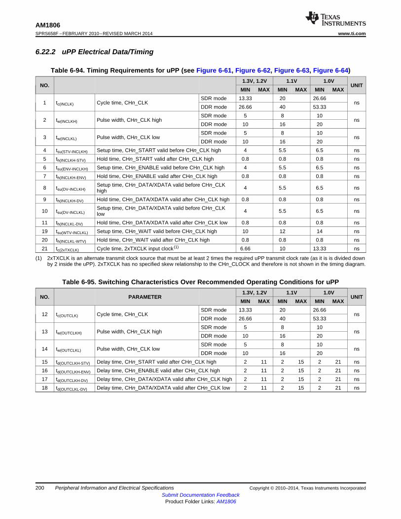
AM1806SPRS658F –FEBRUARY 2010–REVISED MARCH 2014 www.ti.com
6.22.2 uPP Electrical Data/Timing
Table 6-94. Timing Requirements for uPP (see Figure 6-61, Figure 6-62, Figure 6-63, Figure 6-64)1.3V, 1.2V 1.1V 1.0V
NO. UNITMIN MAX MIN MAX MIN MAX
SDR mode 13.33 20 26.661 tc(INCLK) Cycle time, CHn_CLK ns
DDR mode 26.66 40 53.33SDR mode 5 8 10
2 tw(INCLKH) Pulse width, CHn_CLK high nsDDR mode 10 16 20SDR mode 5 8 10
3 tw(INCLKL) Pulse width, CHn_CLK low nsDDR mode 10 16 20
4 tsu(STV-INCLKH) Setup time, CHn_START valid before CHn_CLK high 4 5.5 6.5 ns5 th(INCLKH-STV) Hold time, CHn_START valid after CHn_CLK high 0.8 0.8 0.8 ns6 tsu(ENV-INCLKH) Setup time, CHn_ENABLE valid before CHn_CLK high 4 5.5 6.5 ns7 th(INCLKH-ENV) Hold time, CHn_ENABLE valid after CHn_CLK high 0.8 0.8 0.8 ns
Setup time, CHn_DATA/XDATA valid before CHn_CLK8 tsu(DV-INCLKH) 4 5.5 6.5 nshigh9 th(INCLKH-DV) Hold time, CHn_DATA/XDATA valid after CHn_CLK high 0.8 0.8 0.8 ns
Setup time, CHn_DATA/XDATA valid before CHn_CLK10 tsu(DV-INCLKL) 4 5.5 6.5 nslow11 th(INCLKL-DV) Hold time, CHn_DATA/XDATA valid after CHn_CLK low 0.8 0.8 0.8 ns19 tsu(WTV-INCLKL) Setup time, CHn_WAIT valid before CHn_CLK high 10 12 14 ns20 th(INCLKL-WTV) Hold time, CHn_WAIT valid after CHn_CLK high 0.8 0.8 0.8 ns21 tc(2xTXCLK) Cycle time, 2xTXCLK input clock (1) 6.66 10 13.33 ns
(1) 2xTXCLK is an alternate transmit clock source that must be at least 2 times the required uPP transmit clock rate (as it is is divided downby 2 inside the uPP). 2xTXCLK has no specified skew relationship to the CHn_CLOCK and therefore is not shown in the timing diagram.
Table 6-95. Switching Characteristics Over Recommended Operating Conditions for uPP1.3V, 1.2V 1.1V 1.0V
NO. PARAMETER UNITMIN MAX MIN MAX MIN MAX
SDR mode 13.33 20 26.6612 tc(OUTCLK) Cycle time, CHn_CLK ns
DDR mode 26.66 40 53.33SDR mode 5 8 10
13 tw(OUTCLKH) Pulse width, CHn_CLK high nsDDR mode 10 16 20SDR mode 5 8 10
14 tw(OUTCLKL) Pulse width, CHn_CLK low nsDDR mode 10 16 20
15 td(OUTCLKH-STV) Delay time, CHn_START valid after CHn_CLK high 2 11 2 15 2 21 ns16 td(OUTCLKH-ENV) Delay time, CHn_ENABLE valid after CHn_CLK high 2 11 2 15 2 21 ns17 td(OUTCLKH-DV) Delay time, CHn_DATA/XDATA valid after CHn_CLK high 2 11 2 15 2 21 ns18 td(OUTCLKL-DV) Delay time, CHn_DATA/XDATA valid after CHn_CLK low 2 11 2 15 2 21 ns
200 Peripheral Information and Electrical Specifications Copyright © 2010–2014, Texas Instruments IncorporatedSubmit Documentation Feedback
Product Folder Links: AM1806
I1
21 3
54
76
9
Q1 I2 I3 I4 I5 I6 I7 I8 I9Q2 Q3 Q4 Q5 Q6 Q7 Q8 Q9
8
CHx_CLK
CHx_START
CHx_ENABLE
CHx_DATA[n:0]CHx_XDATA[n:0]
CHx_WAIT
1110
CHx_CLK
CHx_START
CHx_ENABLE
CHx_DATA[n:0]CHx_XDATA[n:0]
Data2Data1 Data3 Data4
2
CHx_WAIT
Data5 Data6
1
Data7 Data8 Data9
3
54
76
98
AM1806www.ti.com SPRS658F –FEBRUARY 2010–REVISED MARCH 2014
Figure 6-61. uPP Single Data Rate (SDR) Receive Timing
Figure 6-62. uPP Double Data Rate (DDR) Receive Timing
Copyright © 2010–2014, Texas Instruments Incorporated Peripheral Information and Electrical Specifications 201Submit Documentation Feedback
Product Folder Links: AM1806
I1
15
13
17
16
12 14
2019
Q1 I2 I3 I4 I5 I6 I7 I8 I9Q2 Q3 Q4 Q5 Q6 Q7 Q8 Q9
18
CHx_CLK
CHx_START
CHx_ENABLE
CHx_DATA[n:0]CHx_XDATA[n:0]
CHx_WAIT
Data2Data1 Data3 Data4
15
13
17
16
Data5 Data6
12
Data7 Data8 Data9
14
2019
CHx_CLK
CHx_START
CHx_ENABLE
CHx_DATA[n:0]CHx_XDATA[n:0]
CHx_WAIT
AM1806SPRS658F –FEBRUARY 2010–REVISED MARCH 2014 www.ti.com
Figure 6-63. uPP Single Data Rate (SDR) Transmit Timing
Figure 6-64. uPP Double Data Rate (DDR) Transmit Timing
202 Peripheral Information and Electrical Specifications Copyright © 2010–2014, Texas Instruments IncorporatedSubmit Documentation Feedback
Product Folder Links: AM1806
AM1806www.ti.com SPRS658F –FEBRUARY 2010–REVISED MARCH 2014
6.23 Video Port Interface (VPIF)The Video Port Interface (VPIF) allows the capture and display of digital video streams. Features include:• Up to 2 Video Capture Channels (Channel 0 and Channel 1)
– Two 8-bit Standard-Definition (SD) Video with embedded timing codes (BT.656)– Single 16-bit High-Definition (HD) Video with embedded timing codes (BT.1120)– Single Raw Video (8-/10-/12-bit)
• Up to 2 Video Display Channels (Channel 2 and Channel 3)– Two 8-bit SD Video Display with embedded timing codes (BT.656)– Single 16-bit HD Video Display with embedded timing codes (BT.1120)
The VPIF capture channel input data format is selectable based on the settings of the specific ChannelControl Register (Channels 0–3). The VPIF Raw Video data-bus width is selectable based on the settingsof the Channel 0 Control Register.
6.23.1 VPIF Register DescriptionsTable 6-96 shows the VPIF registers.
Table 6-96. Video Port Interface (VPIF) RegistersBYTE ADDRESS ACRONYM REGISTER DESCRIPTION
0x01E1 7000 PID Peripheral identification register0x01E1 7004 CH0_CTRL Channel 0 control register0x01E1 7008 CH1_CTRL Channel 1 control register0x01E1 700C CH2_CTRL Channel 2 control register0x01E1 7010 CH3_CTRL Channel 3 control register
0x01E1 7014 - 0x01E1 701F - Reserved0x01E1 7020 INTEN Interrupt enable0x01E1 7024 INTENSET Interrupt enable set0x01E1 7028 INTENCLR Interrupt enable clear0x01E1 702C INTSTAT Interrupt status0x01E1 7030 INTSTATCLR Interrupt status clear0x01E1 7034 EMU_CTRL Emulation control0x01E1 7038 DMA_SIZE DMA size control
0x01E1 703C - 0x01E1 703F - ReservedCAPTURE CHANNEL 0 REGISTERS
0x01E1 7040 CH0_TY_STRTADR Channel 0 Top Field luma buffer start address0x01E1 7044 CH0_BY_STRTADR Channel 0 Bottom Field luma buffer start address0x01E1 7048 CH0_TC_STRTADR Channel 0 Top Field chroma buffer start address0x01E1 704C CH0_BC_STRTADR Channel 0 Bottom Field chroma buffer start address0x01E1 7050 CH0_THA_STRTADR Channel 0 Top Field horizontal ancillary data buffer start address0x01E1 7054 CH0_BHA_STRTADR Channel 0 Bottom Field horizontal ancillary data buffer start address0x01E1 7058 CH0_TVA_STRTADR Channel 0 Top Field vertical ancillary data buffer start address0x01E1 705C CH0_BVA_STRTADR Channel 0 Bottom Field vertical ancillary data buffer start address0x01E1 7060 CH0_SUBPIC_CFG Channel 0 sub-picture configuration0x01E1 7064 CH0_IMG_ADD_OFST Channel 0 image data address offset0x01E1 7068 CH0_HA_ADD_OFST Channel 0 horizontal ancillary data address offset0x01E1 706C CH0_HSIZE_CFG Channel 0 horizontal data size configuration0x01E1 7070 CH0_VSIZE_CFG0 Channel 0 vertical data size configuration (0)0x01E1 7074 CH0_VSIZE_CFG1 Channel 0 vertical data size configuration (1)0x01E1 7078 CH0_VSIZE_CFG2 Channel 0 vertical data size configuration (2)0x01E1 707C CH0_VSIZE Channel 0 vertical image size
Copyright © 2010–2014, Texas Instruments Incorporated Peripheral Information and Electrical Specifications 203Submit Documentation Feedback
Product Folder Links: AM1806

AM1806SPRS658F –FEBRUARY 2010–REVISED MARCH 2014 www.ti.com
Table 6-96. Video Port Interface (VPIF) Registers (continued)BYTE ADDRESS ACRONYM REGISTER DESCRIPTION
CAPTURE CHANNEL 1 REGISTERS0x01E1 7080 CH1_TY_STRTADR Channel 1 Top Field luma buffer start address0x01E1 7084 CH1_BY_STRTADR Channel 1 Bottom Field luma buffer start address0x01E1 7088 CH1_TC_STRTADR Channel 1 Top Field chroma buffer start address0x01E1 708C CH1_BC_STRTADR Channel 1 Bottom Field chroma buffer start address0x01E1 7090 CH1_THA_STRTADR Channel 1 Top Field horizontal ancillary data buffer start address0x01E1 7094 CH1_BHA_STRTADR Channel 1 Bottom Field horizontal ancillary data buffer start address0x01E1 7098 CH1_TVA_STRTADR Channel 1 Top Field vertical ancillary data buffer start address0x01E1 709C CH1_BVA_STRTADR Channel 1 Bottom Field vertical ancillary data buffer start address0x01E1 70A0 CH1_SUBPIC_CFG Channel 1 sub-picture configuration0x01E1 70A4 CH1_IMG_ADD_OFST Channel 1 image data address offset0x01E1 70A8 CH1_HA_ADD_OFST Channel 1 horizontal ancillary data address offset0x01E1 70AC CH1_HSIZE_CFG Channel 1 horizontal data size configuration0x01E1 70B0 CH1_VSIZE_CFG0 Channel 1 vertical data size configuration (0)0x01E1 70B4 CH1_VSIZE_CFG1 Channel 1 vertical data size configuration (1)0x01E1 70B8 CH1_VSIZE_CFG2 Channel 1 vertical data size configuration (2)0x01E1 70BC CH1_VSIZE Channel 1 vertical image size
DISPLAY CHANNEL 2 REGISTERS0x01E1 70C0 CH2_TY_STRTADR Channel 2 Top Field luma buffer start address0x01E1 70C4 CH2_BY_STRTADR Channel 2 Bottom Field luma buffer start address0x01E1 70C8 CH2_TC_STRTADR Channel 2 Top Field chroma buffer start address0x01E1 70CC CH2_BC_STRTADR Channel 2 Bottom Field chroma buffer start address0x01E1 70D0 CH2_THA_STRTADR Channel 2 Top Field horizontal ancillary data buffer start address0x01E1 70D4 CH2_BHA_STRTADR Channel 2 Bottom Field horizontal ancillary data buffer start address0x01E1 70D8 CH2_TVA_STRTADR Channel 2 Top Field vertical ancillary data buffer start address0x01E1 70DC CH2_BVA_STRTADR Channel 2 Bottom Field vertical ancillary data buffer start address0x01E1 70E0 CH2_SUBPIC_CFG Channel 2 sub-picture configuration0x01E1 70E4 CH2_IMG_ADD_OFST Channel 2 image data address offset0x01E1 70E8 CH2_HA_ADD_OFST Channel 2 horizontal ancillary data address offset0x01E1 70EC CH2_HSIZE_CFG Channel 2 horizontal data size configuration0x01E1 70F0 CH2_VSIZE_CFG0 Channel 2 vertical data size configuration (0)0x01E1 70F4 CH2_VSIZE_CFG1 Channel 2 vertical data size configuration (1)0x01E1 70F8 CH2_VSIZE_CFG2 Channel 2 vertical data size configuration (2)0x01E1 70FC CH2_VSIZE Channel 2 vertical image size0x01E1 7100 CH2_THA_STRTPOS Channel 2 Top Field horizontal ancillary data insertion start position0x01E1 7104 CH2_THA_SIZE Channel 2 Top Field horizontal ancillary data size0x01E1 7108 CH2_BHA_STRTPOS Channel 2 Bottom Field horizontal ancillary data insertion start position0x01E1 710C CH2_BHA_SIZE Channel 2 Bottom Field horizontal ancillary data size0x01E1 7110 CH2_TVA_STRTPOS Channel 2 Top Field vertical ancillary data insertion start position0x01E1 7114 CH2_TVA_SIZE Channel 2 Top Field vertical ancillary data size0x01E1 7118 CH2_BVA_STRTPOS Channel 2 Bottom Field vertical ancillary data insertion start position0x01E1 711C CH2_BVA_SIZE Channel 2 Bottom Field vertical ancillary data size
0x01E1 7120 - 0x01E1 713F - ReservedDISPLAY CHANNEL 3 REGISTERS
0x01E1 7140 CH3_TY_STRTADR Channel 3 Field 0 luma buffer start address0x01E1 7144 CH3_BY_STRTADR Channel 3 Field 1 luma buffer start address0x01E1 7148 CH3_TC_STRTADR Channel 3 Field 0 chroma buffer start address
204 Peripheral Information and Electrical Specifications Copyright © 2010–2014, Texas Instruments IncorporatedSubmit Documentation Feedback
Product Folder Links: AM1806
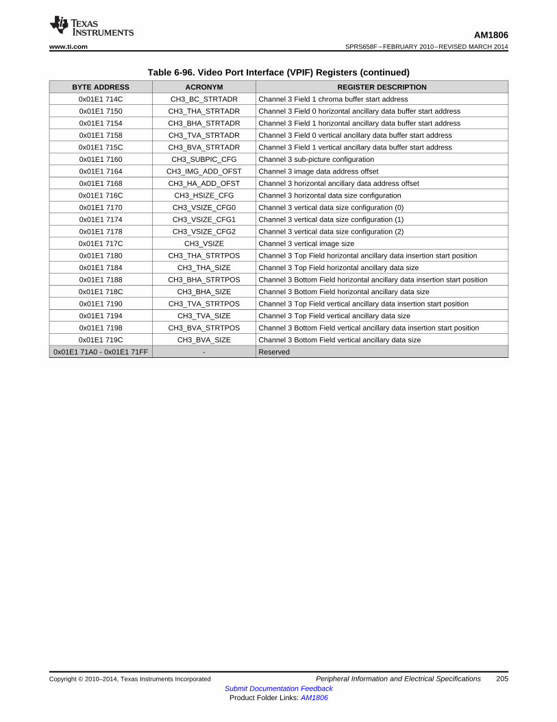
AM1806www.ti.com SPRS658F –FEBRUARY 2010–REVISED MARCH 2014
Table 6-96. Video Port Interface (VPIF) Registers (continued)BYTE ADDRESS ACRONYM REGISTER DESCRIPTION
0x01E1 714C CH3_BC_STRTADR Channel 3 Field 1 chroma buffer start address0x01E1 7150 CH3_THA_STRTADR Channel 3 Field 0 horizontal ancillary data buffer start address0x01E1 7154 CH3_BHA_STRTADR Channel 3 Field 1 horizontal ancillary data buffer start address0x01E1 7158 CH3_TVA_STRTADR Channel 3 Field 0 vertical ancillary data buffer start address0x01E1 715C CH3_BVA_STRTADR Channel 3 Field 1 vertical ancillary data buffer start address0x01E1 7160 CH3_SUBPIC_CFG Channel 3 sub-picture configuration0x01E1 7164 CH3_IMG_ADD_OFST Channel 3 image data address offset0x01E1 7168 CH3_HA_ADD_OFST Channel 3 horizontal ancillary data address offset0x01E1 716C CH3_HSIZE_CFG Channel 3 horizontal data size configuration0x01E1 7170 CH3_VSIZE_CFG0 Channel 3 vertical data size configuration (0)0x01E1 7174 CH3_VSIZE_CFG1 Channel 3 vertical data size configuration (1)0x01E1 7178 CH3_VSIZE_CFG2 Channel 3 vertical data size configuration (2)0x01E1 717C CH3_VSIZE Channel 3 vertical image size0x01E1 7180 CH3_THA_STRTPOS Channel 3 Top Field horizontal ancillary data insertion start position0x01E1 7184 CH3_THA_SIZE Channel 3 Top Field horizontal ancillary data size0x01E1 7188 CH3_BHA_STRTPOS Channel 3 Bottom Field horizontal ancillary data insertion start position0x01E1 718C CH3_BHA_SIZE Channel 3 Bottom Field horizontal ancillary data size0x01E1 7190 CH3_TVA_STRTPOS Channel 3 Top Field vertical ancillary data insertion start position0x01E1 7194 CH3_TVA_SIZE Channel 3 Top Field vertical ancillary data size0x01E1 7198 CH3_BVA_STRTPOS Channel 3 Bottom Field vertical ancillary data insertion start position0x01E1 719C CH3_BVA_SIZE Channel 3 Bottom Field vertical ancillary data size
0x01E1 71A0 - 0x01E1 71FF - Reserved
Copyright © 2010–2014, Texas Instruments Incorporated Peripheral Information and Electrical Specifications 205Submit Documentation Feedback
Product Folder Links: AM1806
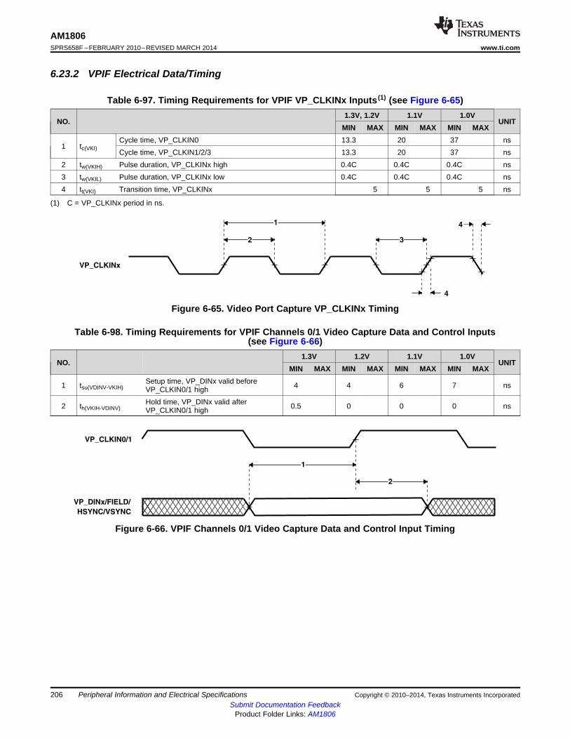
VP_CLKIN0/1
VP_DINx/FIELD/
HSYNC/VSYNC
1
2
VP_CLKINx
2 3
1 4
4
AM1806SPRS658F –FEBRUARY 2010–REVISED MARCH 2014 www.ti.com
6.23.2 VPIF Electrical Data/Timing
Table 6-97. Timing Requirements for VPIF VP_CLKINx Inputs (1) (see Figure 6-65)1.3V, 1.2V 1.1V 1.0V
NO. UNITMIN MAX MIN MAX MIN MAX
Cycle time, VP_CLKIN0 13.3 20 37 ns1 tc(VKI) Cycle time, VP_CLKIN1/2/3 13.3 20 37 ns2 tw(VKIH) Pulse duration, VP_CLKINx high 0.4C 0.4C 0.4C ns3 tw(VKIL) Pulse duration, VP_CLKINx low 0.4C 0.4C 0.4C ns4 tt(VKI) Transition time, VP_CLKINx 5 5 5 ns
(1) C = VP_CLKINx period in ns.
Figure 6-65. Video Port Capture VP_CLKINx Timing
Table 6-98. Timing Requirements for VPIF Channels 0/1 Video Capture Data and Control Inputs(see Figure 6-66)
1.3V 1.2V 1.1V 1.0VNO. UNIT
MIN MAX MIN MAX MIN MAX MIN MAXSetup time, VP_DINx valid before1 tsu(VDINV-VKIH) 4 4 6 7 nsVP_CLKIN0/1 highHold time, VP_DINx valid after2 th(VKIH-VDINV) 0.5 0 0 0 nsVP_CLKIN0/1 high
Figure 6-66. VPIF Channels 0/1 Video Capture Data and Control Input Timing
206 Peripheral Information and Electrical Specifications Copyright © 2010–2014, Texas Instruments IncorporatedSubmit Documentation Feedback
Product Folder Links: AM1806
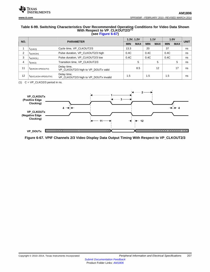
VP_CLKOUTx
(Positive Edge
Clocking)
VP_CLKOUTx
(Negative Edge
Clocking)
VP_DOUTx
12
11 12
44
3
AM1806www.ti.com SPRS658F –FEBRUARY 2010–REVISED MARCH 2014
Table 6-99. Switching Characteristics Over Recommended Operating Conditions for Video Data ShownWith Respect to VP_CLKOUT2/3 (1)
(see Figure 6-67)1.3V, 1.2V 1.1V 1.0V
NO. PARAMETER UNITMIN MAX MIN MAX MIN MAX
1 tc(VKO) Cycle time, VP_CLKOUT2/3 13.3 20 37 ns2 tw(VKOH) Pulse duration, VP_CLKOUT2/3 high 0.4C 0.4C 0.4C ns3 tw(VKOL) Pulse duration, VP_CLKOUT2/3 low 0.4C 0.4C 0.4C ns4 tt(VKO) Transition time, VP_CLKOUT2/3 5 5 5 ns
Delay time,11 td(VKOH-VPDOUTV) 8.5 12 17 nsVP_CLKOUT2/3 high to VP_DOUTx validDelay time,12 td(VCLKOH-VPDOUTIV) 1.5 1.5 1.5 nsVP_CLKOUT2/3 high to VP_DOUTx invalid
(1) C = VP_CLKO2/3 period in ns.
Figure 6-67. VPIF Channels 2/3 Video Display Data Output Timing With Respect to VP_CLKOUT2/3
Copyright © 2010–2014, Texas Instruments Incorporated Peripheral Information and Electrical Specifications 207Submit Documentation Feedback
Product Folder Links: AM1806
AM1806SPRS658F –FEBRUARY 2010–REVISED MARCH 2014 www.ti.com
6.24 Enhanced Capture (eCAP) PeripheralThe device contains up to three enhanced capture (eCAP) modules. Figure 6-68 shows a functional blockdiagram of a module.
Uses for ECAP include:• Speed measurements of rotating machinery (e.g. toothed sprockets sensed via Hall sensors)• Elapsed time measurements between position sensor triggers• Period and duty cycle measurements of pulse train signals• Decoding current or voltage amplitude derived from duty cycle encoded current/voltage sensors
The ECAP module described in this specification includes the following features:• 32 bit time base• 4 event time-stamp registers (each 32 bits)• Edge polarity selection for up to 4 sequenced time-stamp capture events• Interrupt on either of the 4 events• Single shot capture of up to 4 event time-stamps• Continuous mode capture of time-stamps in a 4 deep circular buffer• Absolute time-stamp capture• Difference mode time-stamp capture• All the above resources are dedicated to a single input pin
The eCAP modules are clocked at the ASYNC3 clock domain rate.
208 Peripheral Information and Electrical Specifications Copyright © 2010–2014, Texas Instruments IncorporatedSubmit Documentation Feedback
Product Folder Links: AM1806
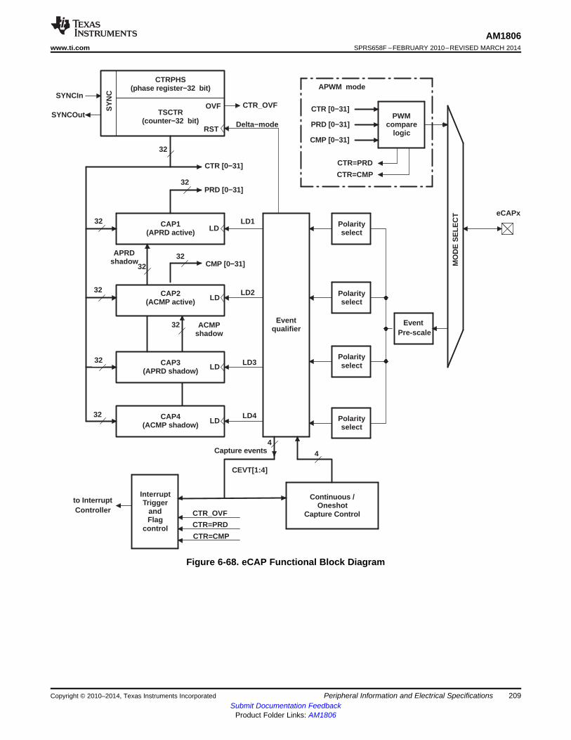
TSCTR(counter−32 bit)
RST
CAP1(APRD active) LD
CAP2(ACMP active) LD
CAP3(APRD shadow) LD
CAP4(ACMP shadow) LD
Continuous /Oneshot
Capture Control
LD1
LD2
LD3
LD4
32
32
PRD [0−31]
CMP [0−31]
CTR [0−31]
eCAPx
InterruptTrigger
andFlag
control
to InterruptController
CTR=CMP
32
32
32
32
32
ACMPshadow
Event Pre-scale
CTRPHS(phase register−32 bit)
SYNCOut
SYNCIn
Eventqualifier
Polarityselect
Polarityselect
Polarityselect
Polarityselect
CTR=PRD
CTR_OVF
4
PWMcompare
logic
CTR [0−31]
PRD [0−31]
CMP [0−31]
CTR=CMP
CTR=PRD
CTR_OVFOVF
APWM mode
Delta−mode
SY
NC
4Capture events
CEVT[1:4]
APRDshadow
32
32 MO
DE
SE
LEC
T
AM1806www.ti.com SPRS658F –FEBRUARY 2010–REVISED MARCH 2014
Figure 6-68. eCAP Functional Block Diagram
Copyright © 2010–2014, Texas Instruments Incorporated Peripheral Information and Electrical Specifications 209Submit Documentation Feedback
Product Folder Links: AM1806
AM1806SPRS658F –FEBRUARY 2010–REVISED MARCH 2014 www.ti.com
Table 6-100 is the list of the ECAP registers.
Table 6-100. ECAPx Configuration Registers
ECAP0 ECAP1 ECAP2 ACRONYM DESCRIPTIONBYTE ADDRESS BYTE ADDRESS BYTE ADDRESS0x01F0 6000 0x01F0 7000 0x01F0 8000 TSCTR Time-Stamp Counter0x01F0 6004 0x01F0 7004 0x01F0 8004 CTRPHS Counter Phase Offset Value Register0x01F0 6008 0x01F0 7008 0x01F0 8008 CAP1 Capture 1 Register0x01F0 600C 0x01F0 700C 0x01F0 800C CAP2 Capture 2 Register0x01F0 6010 0x01F0 7010 0x01F0 8010 CAP3 Capture 3 Register0x01F0 6014 0x01F0 7014 0x01F0 8014 CAP4 Capture 4 Register0x01F0 6028 0x01F0 7028 0x01F0 8028 ECCTL1 Capture Control Register 10x01F0 602A 0x01F0 702A 0x01F0 802A ECCTL2 Capture Control Register 20x01F0 602C 0x01F0 702C 0x01F0 802C ECEINT Capture Interrupt Enable Register0x01F0 602E 0x01F0 702E 0x01F0 802E ECFLG Capture Interrupt Flag Register0x01F0 6030 0x01F0 7030 0x01F0 8030 ECCLR Capture Interrupt Clear Register0x01F0 6032 0x01F0 7032 0x01F0 8032 ECFRC Capture Interrupt Force Register0x01F0 605C 0x01F0 705C 0x01F0 805C REVID Revision ID
Table 6-101 shows the eCAP timing requirement and Table 6-102 shows the eCAP switchingcharacteristics.
Table 6-101. Timing Requirements for Enhanced Capture (eCAP)TEST 1.3V, 1.2V, 1.1V, 1.0V UNIT
CONDITIONS MIN MAXtw(CAP) Capture input pulse width Asynchronous 2tc(SCO) cycles
Synchronous 2tc(SCO) cycles
Table 6-102. Switching Characteristics Over Recommended Operating Conditions for eCAPPARAMETER 1.3V, 1.2V 1.1V 1.0V UNIT
MIN MAX MIN MAX MIN MAXtw(APWM) Pulse duration, APWMx 20 20 20 ns
output high/low
210 Peripheral Information and Electrical Specifications Copyright © 2010–2014, Texas Instruments IncorporatedSubmit Documentation Feedback
Product Folder Links: AM1806
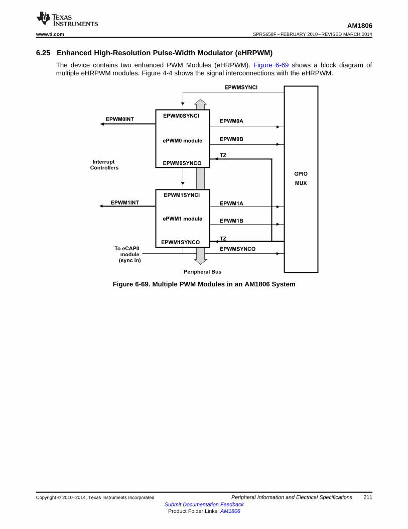
Peripheral Bus
ePWM0 module
ePWM1 module
EPWM0SYNCI
EPWM1SYNCI
EPWM1SYNCO
GPIO
MUX
EPWMSYNCI
EPWM1A
EPWM1B
EPWM0A
EPWM0B
EPWM0INT
EPWM1INT
TZ
TZ
EPWM0SYNCOInterruptControllers
EPWMSYNCOTo eCAP0module(sync in)
AM1806www.ti.com SPRS658F –FEBRUARY 2010–REVISED MARCH 2014
6.25 Enhanced High-Resolution Pulse-Width Modulator (eHRPWM)The device contains two enhanced PWM Modules (eHRPWM). Figure 6-69 shows a block diagram ofmultiple eHRPWM modules. Figure 4-4 shows the signal interconnections with the eHRPWM.
Figure 6-69. Multiple PWM Modules in an AM1806 System
Copyright © 2010–2014, Texas Instruments Incorporated Peripheral Information and Electrical Specifications 211Submit Documentation Feedback
Product Folder Links: AM1806
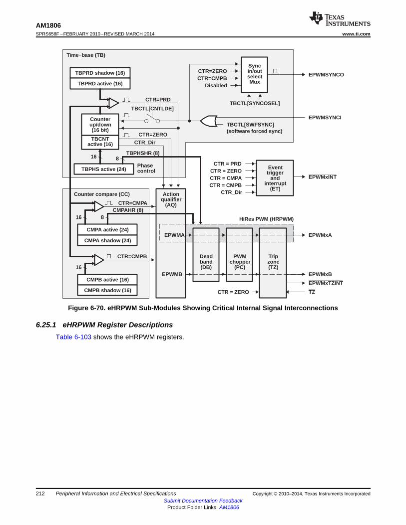
CTR=PRD
TBPRD shadow (16)
TBPRD active (16)
Counterup/down(16 bit)
TBCNTactive (16)
TBCTL[CNTLDE]
TBCTL[SWFSYNC](software forced sync)
EPWMSYNCI
CTR=ZERO
CTR_Dir
CTR=CMPBDisabled
Syncin/outselectMux
TBCTL[SYNCOSEL]
EPWMSYNCO
TBPHS active (24)
16 8TBPHSHR (8)
Phasecontrol
Time−base (TB)
CTR=CMPA
CMPA active (24)
16
CMPA shadow (24)
Actionqualifier
(AQ)
8
16
Counter compare (CC)
CMPB active (16)
CTR=CMPB
CMPB shadow (16)
CMPAHR (8)
EPWMA
EPWMB
Deadband(DB) (PC)
chopperPWM
zone(TZ)
Trip
CTR = ZERO
EPWMxA
EPWMxB
EPWMxTZINT
TZ
HiRes PWM (HRPWM)
CTR = PRDCTR = ZERO
CTR = CMPBCTR = CMPA
CTR_Dir
Eventtrigger
andinterrupt
(ET)
EPWMxINT
CTR=ZERO
AM1806SPRS658F –FEBRUARY 2010–REVISED MARCH 2014 www.ti.com
Figure 6-70. eHRPWM Sub-Modules Showing Critical Internal Signal Interconnections
6.25.1 eHRPWM Register DescriptionsTable 6-103 shows the eHRPWM registers.
212 Peripheral Information and Electrical Specifications Copyright © 2010–2014, Texas Instruments IncorporatedSubmit Documentation Feedback
Product Folder Links: AM1806
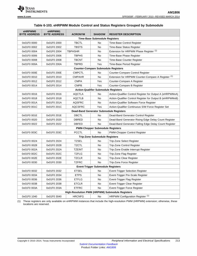
AM1806www.ti.com SPRS658F –FEBRUARY 2010–REVISED MARCH 2014
Table 6-103. eHRPWM Module Control and Status Registers Grouped by Submodule
eHRPWM0 eHRPWM1BYTE ADDRESS BYTE ADDRESS ACRONYM SHADOW REGISTER DESCRIPTION
Time-Base Submodule Registers0x01F0 0000 0x01F0 2000 TBCTL No Time-Base Control Register0x01F0 0002 0x01F0 2002 TBSTS No Time-Base Status Register0x01F0 0004 0x01F0 2004 TBPHSHR No Extension for HRPWM Phase Register (1)
0x01F0 0006 0x01F0 2006 TBPHS No Time-Base Phase Register0x01F0 0008 0x01F0 2008 TBCNT No Time-Base Counter Register0x01F0 000A 0x01F0 200A TBPRD Yes Time-Base Period Register
Counter-Compare Submodule Registers0x01F0 000E 0x01F0 200E CMPCTL No Counter-Compare Control Register0x01F0 0010 0x01F0 2010 CMPAHR No Extension for HRPWM Counter-Compare A Register (1)
0x01F0 0012 0x01F0 2012 CMPA Yes Counter-Compare A Register0x01F0 0014 0x01F0 2014 CMPB Yes Counter-Compare B Register
Action-Qualifier Submodule Registers0x01F0 0016 0x01F0 2016 AQCTLA No Action-Qualifier Control Register for Output A (eHRPWMxA)0x01F0 0018 0x01F0 2018 AQCTLB No Action-Qualifier Control Register for Output B (eHRPWMxB)0x01F0 001A 0x01F0 201A AQSFRC No Action-Qualifier Software Force Register0x01F0 001C 0x01F0 201C AQCSFRC Yes Action-Qualifier Continuous S/W Force Register Set
Dead-Band Generator Submodule Registers0x01F0 001E 0x01F0 201E DBCTL No Dead-Band Generator Control Register0x01F0 0020 0x01F0 2020 DBRED No Dead-Band Generator Rising Edge Delay Count Register0x01F0 0022 0x01F0 2022 DBFED No Dead-Band Generator Falling Edge Delay Count Register
PWM-Chopper Submodule Registers0x01F0 003C 0x01F0 203C PCCTL No PWM-Chopper Control Register
Trip-Zone Submodule Registers0x01F0 0024 0x01F0 2024 TZSEL No Trip-Zone Select Register0x01F0 0028 0x01F0 2028 TZCTL No Trip-Zone Control Register0x01F0 002A 0x01F0 202A TZEINT No Trip-Zone Enable Interrupt Register0x01F0 002C 0x01F0 202C TZFLG No Trip-Zone Flag Register0x01F0 002E 0x01F0 202E TZCLR No Trip-Zone Clear Register0x01F0 0030 0x01F0 2030 TZFRC No Trip-Zone Force Register
Event-Trigger Submodule Registers0x01F0 0032 0x01F0 2032 ETSEL No Event-Trigger Selection Register0x01F0 0034 0x01F0 2034 ETPS No Event-Trigger Pre-Scale Register0x01F0 0036 0x01F0 2036 ETFLG No Event-Trigger Flag Register0x01F0 0038 0x01F0 2038 ETCLR No Event-Trigger Clear Register0x01F0 003A 0x01F0 203A ETFRC No Event-Trigger Force Register
High-Resolution PWM (HRPWM) Submodule Registers0x01F0 1040 0x01F0 3040 HRCNFG No HRPWM Configuration Register (1)
(1) These registers are only available on eHRPWM instances that include the high-resolution PWM (HRPWM) extension; otherwise, theselocations are reserved.
Copyright © 2010–2014, Texas Instruments Incorporated Peripheral Information and Electrical Specifications 213Submit Documentation Feedback
Product Folder Links: AM1806
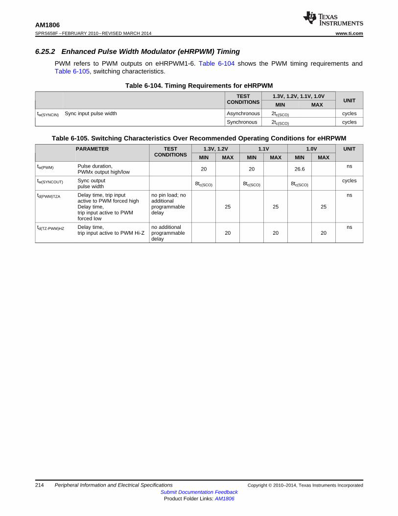
AM1806SPRS658F –FEBRUARY 2010–REVISED MARCH 2014 www.ti.com
6.25.2 Enhanced Pulse Width Modulator (eHRPWM) TimingPWM refers to PWM outputs on eHRPWM1-6. Table 6-104 shows the PWM timing requirements andTable 6-105, switching characteristics.
Table 6-104. Timing Requirements for eHRPWMTEST 1.3V, 1.2V, 1.1V, 1.0V
UNITCONDITIONS MIN MAXtw(SYNCIN) Sync input pulse width Asynchronous 2tc(SCO) cycles
Synchronous 2tc(SCO) cycles
Table 6-105. Switching Characteristics Over Recommended Operating Conditions for eHRPWMPARAMETER TEST 1.3V, 1.2V 1.1V 1.0V UNIT
CONDITIONS MIN MAX MIN MAX MIN MAXtw(PWM) Pulse duration, ns20 20 26.6PWMx output high/lowtw(SYNCOUT) Sync output cycles8tc(SCO) 8tc(SCO) 8tc(SCO)pulse widthtd(PWM)TZA Delay time, trip input no pin load; no ns
active to PWM forced high additionalDelay time, programmable 25 25 25trip input active to PWM delayforced low
td(TZ-PWM)HZ Delay time, no additional nstrip input active to PWM Hi-Z programmable 20 20 20
delay
214 Peripheral Information and Electrical Specifications Copyright © 2010–2014, Texas Instruments IncorporatedSubmit Documentation Feedback
Product Folder Links: AM1806
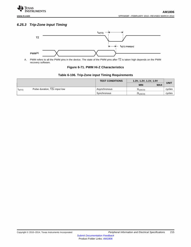
PWM(A)
TZ
tw(TZ)
td(TZ-PWM)HZ
AM1806www.ti.com SPRS658F –FEBRUARY 2010–REVISED MARCH 2014
6.25.3 Trip-Zone Input Timing
A. PWM refers to all the PWM pins in the device. The state of the PWM pins after TZ is taken high depends on the PWMrecovery software.
Figure 6-71. PWM Hi-Z Characteristics
Table 6-106. Trip-Zone input Timing Requirements
TEST CONDITIONS 1.3V, 1.2V, 1.1V, 1.0VUNIT
MIN MAXtw(TZ) Pulse duration, TZx input low Asynchronous 1tc(SCO) cycles
Synchronous 2tc(SCO) cycles
Copyright © 2010–2014, Texas Instruments Incorporated Peripheral Information and Electrical Specifications 215Submit Documentation Feedback
Product Folder Links: AM1806
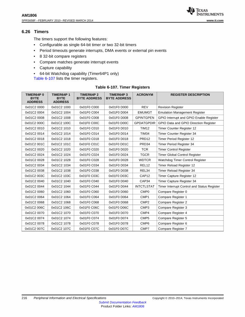
AM1806SPRS658F –FEBRUARY 2010–REVISED MARCH 2014 www.ti.com
6.26 TimersThe timers support the following features:• Configurable as single 64-bit timer or two 32-bit timers• Period timeouts generate interrupts, DMA events or external pin events• 8 32-bit compare registers• Compare matches generate interrupt events• Capture capability• 64-bit Watchdog capability (Timer64P1 only)Table 6-107 lists the timer registers.
Table 6-107. Timer Registers
TIMER64P 0 TIMER64P 1 TIMER64P 2 TIMER64P 3 ACRONYM REGISTER DESCRIPTIONBYTE BYTE BYTE ADDRESS BYTE ADDRESS
ADDRESS ADDRESS0x01C2 0000 0x01C2 1000 0x01F0 C000 0x01F0 D000 REV Revision Register0x01C2 0004 0x01C2 1004 0x01F0 C004 0x01F0 D004 EMUMGT Emulation Management Register0x01C2 0008 0x01C2 1008 0x01F0 C008 0x01F0 D008 GPINTGPEN GPIO Interrupt and GPIO Enable Register0x01C2 000C 0x01C2 100C 0x01F0 C00C 0x01F0 D00C GPDATGPDIR GPIO Data and GPIO Direction Register0x01C2 0010 0x01C2 1010 0x01F0 C010 0x01F0 D010 TIM12 Timer Counter Register 120x01C2 0014 0x01C2 1014 0x01F0 C014 0x01F0 D014 TIM34 Timer Counter Register 340x01C2 0018 0x01C2 1018 0x01F0 C018 0x01F0 D018 PRD12 Timer Period Register 120x01C2 001C 0x01C2 101C 0x01F0 C01C 0x01F0 D01C PRD34 Timer Period Register 340x01C2 0020 0x01C2 1020 0x01F0 C020 0x01F0 D020 TCR Timer Control Register0x01C2 0024 0x01C2 1024 0x01F0 C024 0x01F0 D024 TGCR Timer Global Control Register0x01C2 0028 0x01C2 1028 0x01F0 C028 0x01F0 D028 WDTCR Watchdog Timer Control Register0x01C2 0034 0x01C2 1034 0x01F0 C034 0x01F0 D034 REL12 Timer Reload Register 120x01C2 0038 0x01C2 1038 0x01F0 C038 0x01F0 D038 REL34 Timer Reload Register 340x01C2 003C 0x01C2 103C 0x01F0 C03C 0x01F0 D03C CAP12 Timer Capture Register 120x01C2 0040 0x01C2 1040 0x01F0 C040 0x01F0 D040 CAP34 Timer Capture Register 340x01C2 0044 0x01C2 1044 0x01F0 C044 0x01F0 D044 INTCTLSTAT Timer Interrupt Control and Status Register0x01C2 0060 0x01C2 1060 0x01F0 C060 0x01F0 D060 CMP0 Compare Register 00x01C2 0064 0x01C2 1064 0x01F0 C064 0x01F0 D064 CMP1 Compare Register 10x01C2 0068 0x01C2 1068 0x01F0 C068 0x01F0 D068 CMP2 Compare Register 20x01C2 006C 0x01C2 106C 0x01F0 C06C 0x01F0 D06C CMP3 Compare Register 30x01C2 0070 0x01C2 1070 0x01F0 C070 0x01F0 D070 CMP4 Compare Register 40x01C2 0074 0x01C2 1074 0x01F0 C074 0x01F0 D074 CMP5 Compare Register 50x01C2 0078 0x01C2 1078 0x01F0 C078 0x01F0 D078 CMP6 Compare Register 60x01C2 007C 0x01C2 107C 0x01F0 C07C 0x01F0 D07C CMP7 Compare Register 7
216 Peripheral Information and Electrical Specifications Copyright © 2010–2014, Texas Instruments IncorporatedSubmit Documentation Feedback
Product Folder Links: AM1806
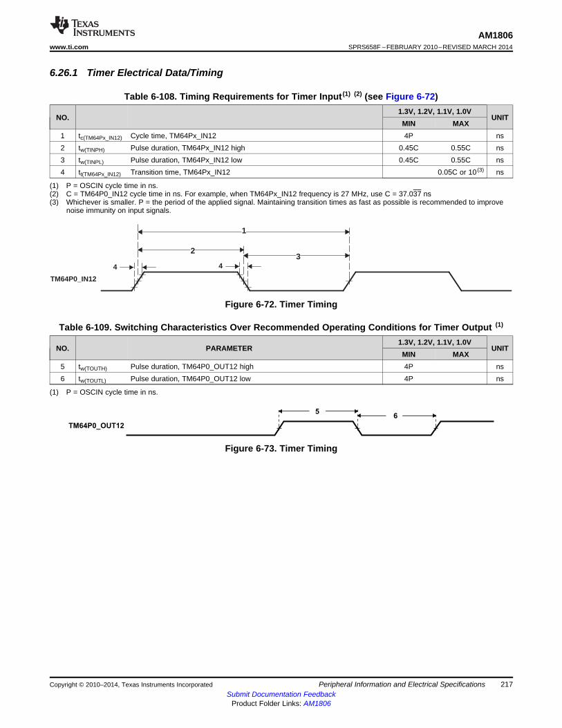
TM64P0_OUT12
56
1
2
443
TM64P0_IN12
AM1806www.ti.com SPRS658F –FEBRUARY 2010–REVISED MARCH 2014
6.26.1 Timer Electrical Data/Timing
Table 6-108. Timing Requirements for Timer Input (1) (2) (see Figure 6-72)1.3V, 1.2V, 1.1V, 1.0V
NO. UNITMIN MAX
1 tc(TM64Px_IN12) Cycle time, TM64Px_IN12 4P ns2 tw(TINPH) Pulse duration, TM64Px_IN12 high 0.45C 0.55C ns3 tw(TINPL) Pulse duration, TM64Px_IN12 low 0.45C 0.55C ns4 tt(TM64Px_IN12) Transition time, TM64Px_IN12 0.05C or 10 (3) ns
(1) P = OSCIN cycle time in ns.(2) C = TM64P0_IN12 cycle time in ns. For example, when TM64Px_IN12 frequency is 27 MHz, use C = 37.037 ns(3) Whichever is smaller. P = the period of the applied signal. Maintaining transition times as fast as possible is recommended to improve
noise immunity on input signals.
Figure 6-72. Timer Timing
Table 6-109. Switching Characteristics Over Recommended Operating Conditions for Timer Output (1)
1.3V, 1.2V, 1.1V, 1.0VNO. PARAMETER UNIT
MIN MAX5 tw(TOUTH) Pulse duration, TM64P0_OUT12 high 4P ns6 tw(TOUTL) Pulse duration, TM64P0_OUT12 low 4P ns
(1) P = OSCIN cycle time in ns.
Figure 6-73. Timer Timing
Copyright © 2010–2014, Texas Instruments Incorporated Peripheral Information and Electrical Specifications 217Submit Documentation Feedback
Product Folder Links: AM1806
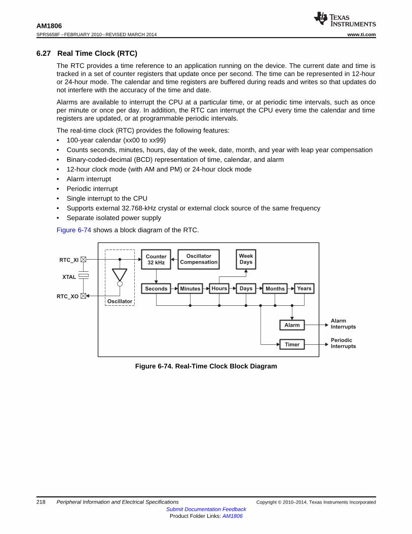
Seconds Minutes Hours Days Months Years
Alarm
Timer
AlarmInterrupts
PeriodicInterrupts
Counter32 kHz
OscillatorCompensation
WeekDays
Oscillator
RTC_XI
XTAL
RTC_XO
AM1806SPRS658F –FEBRUARY 2010–REVISED MARCH 2014 www.ti.com
6.27 Real Time Clock (RTC)The RTC provides a time reference to an application running on the device. The current date and time istracked in a set of counter registers that update once per second. The time can be represented in 12-houror 24-hour mode. The calendar and time registers are buffered during reads and writes so that updates donot interfere with the accuracy of the time and date.
Alarms are available to interrupt the CPU at a particular time, or at periodic time intervals, such as onceper minute or once per day. In addition, the RTC can interrupt the CPU every time the calendar and timeregisters are updated, or at programmable periodic intervals.
The real-time clock (RTC) provides the following features:• 100-year calendar (xx00 to xx99)• Counts seconds, minutes, hours, day of the week, date, month, and year with leap year compensation• Binary-coded-decimal (BCD) representation of time, calendar, and alarm• 12-hour clock mode (with AM and PM) or 24-hour clock mode• Alarm interrupt• Periodic interrupt• Single interrupt to the CPU• Supports external 32.768-kHz crystal or external clock source of the same frequency• Separate isolated power supply
Figure 6-74 shows a block diagram of the RTC.
Figure 6-74. Real-Time Clock Block Diagram
218 Peripheral Information and Electrical Specifications Copyright © 2010–2014, Texas Instruments IncorporatedSubmit Documentation Feedback
Product Folder Links: AM1806
XTAL32.768
kHz
C2
C1
RTC_XI
RTC_XO
RTC_VSS
32KOSC
RealTimeClock(RTC)
Module
Isolated RTCPower Domain
CVDD
RTC_CVDD
RTCPowerSource
AM1806www.ti.com SPRS658F –FEBRUARY 2010–REVISED MARCH 2014
6.27.1 Clock SourceThe clock reference for the RTC is an external 32.768-kHz crystal or an external clock source of the samefrequency. The RTC also has a separate power supply that is isolated from the rest of the system. Whenthe CPU and other peripherals are without power, the RTC can remain powered to preserve the currenttime and calendar information. Even if the RTC is not used, it must remain powered when the rest of thedevice is powered.
The source for the RTC reference clock may be provided by a crystal or by an external clock source. TheRTC has an internal oscillator buffer to support direct operation with a crystal. The crystal is connectedbetween pins RTC_XI and RTC_XO. RTC_XI is the input to the on-chip oscillator and RTC_XO is theoutput from the oscillator back to the crystal.
An external 32.768-kHz clock source may be used instead of a crystal. In such a case, the clock source isconnected to RTC_XI, and RTC_XO is left unconnected.
If the RTC is not used, the RTC_XI pin should be held either low or high, RTC_XO should be leftunconnected, RTC_CVDD should be connected to the device CVDD and RTC_VSS should remaingrounded.
Figure 6-75. Clock Source
Copyright © 2010–2014, Texas Instruments Incorporated Peripheral Information and Electrical Specifications 219Submit Documentation Feedback
Product Folder Links: AM1806
AM1806SPRS658F –FEBRUARY 2010–REVISED MARCH 2014 www.ti.com
6.27.2 Real-Time Clock Register Descriptions
Table 6-110. Real-Time Clock (RTC) Registers
BYTE ADDRESS ACRONYM REGISTER DESCRIPTION0x01C2 3000 SECOND Seconds Register0x01C2 3004 MINUTE Minutes Register0x01C2 3008 HOUR Hours Register0x01C2 300C DAY Day of the Month Register0x01C2 3010 MONTH Month Register0x01C2 3014 YEAR Year Register0x01C2 3018 DOTW Day of the Week Register0x01C2 3020 ALARMSECOND Alarm Seconds Register0x01C2 3024 ALARMMINUTE Alarm Minutes Register0x01C2 3028 ALARMHOUR Alarm Hours Register0x01C2 302C ALARMDAY Alarm Days Register0x01C2 3030 ALARMMONTH Alarm Months Register0x01C2 3034 ALARMYEAR Alarm Years Register0x01C2 3040 CTRL Control Register0x01C2 3044 STATUS Status Register0x01C2 3048 INTERRUPT Interrupt Enable Register0x01C2 304C COMPLSB Compensation (LSB) Register0x01C2 3050 COMPMSB Compensation (MSB) Register0x01C2 3054 OSC Oscillator Register0x01C2 3060 SCRATCH0 Scratch 0 (General-Purpose) Register0x01C2 3064 SCRATCH1 Scratch 1 (General-Purpose) Register0x01C2 3068 SCRATCH2 Scratch 2 (General-Purpose) Register0x01C2 306C KICK0 Kick 0 (Write Protect) Register0x01C2 3070 KICK1 Kick 1 (Write Protect) Register
220 Peripheral Information and Electrical Specifications Copyright © 2010–2014, Texas Instruments IncorporatedSubmit Documentation Feedback
Product Folder Links: AM1806
AM1806www.ti.com SPRS658F –FEBRUARY 2010–REVISED MARCH 2014
6.28 General-Purpose Input/Output (GPIO)The GPIO peripheral provides general-purpose pins that can be configured as either inputs or outputs.When configured as an output, a write to an internal register can control the state driven on the output pin.When configured as an input, the state of the input is detectable by reading the state of an internalregister. In addition, the GPIO peripheral can produce CPU interrupts and EDMA events in differentinterrupt/event generation modes. The GPIO peripheral provides generic connections to external devices.The GPIO pins are grouped into banks of 16 pins per bank (i.e., bank 0 consists of GPIO [0:15]).
The device GPIO peripheral supports the following:• Up to 144 Pins configurable as GPIO• External Interrupt and DMA request Capability
– Every GPIO pin may be configured to generate an interrupt request on detection of rising and/orfalling edges on the pin.
– The interrupt requests within each bank are combined (logical or) to create eight unique bank levelinterrupt requests.
– The bank level interrupt service routine may poll the INTSTATx register for its bank to determinewhich pin(s) have triggered the interrupt.
– GPIO Banks 0, 1, 2, 3, 4, 5, 6, 7 and 8 Interrupts assigned to ARM INTC Interrupt Requests 42, 43,44, 45, 46, 47, 48, 49 and 50 respectively
– GPIO Banks 0, 1, 2, 3, 4, and 5 are assigned to EDMA events 6, 7, 22, 23, 28, 29, and 29respectively on Channel Controller 0 and GPIO Banks 6, 7, and 8 are assigned to EDMA events16, 17, and 18 respectively on Channel Controller 1.
• Set/clear functionality: Firmware writes 1 to corresponding bit position(s) to set or to clear GPIOsignal(s). This allows multiple firmware processes to toggle GPIO output signals without critical sectionprotection (disable interrupts, program GPIO, re-enable interrupts, to prevent context switching toanther process during GPIO programming).
• Separate Input/Output registers• Output register in addition to set/clear so that, if preferred by firmware, some GPIO output signals can
be toggled by direct write to the output register(s).• Output register, when read, reflects output drive status. This, in addition to the input register reflecting
pin status and open-drain I/O cell, allows wired logic be implemented.
The memory map for the GPIO registers is shown in Table 6-111.
Copyright © 2010–2014, Texas Instruments Incorporated Peripheral Information and Electrical Specifications 221Submit Documentation Feedback
Product Folder Links: AM1806
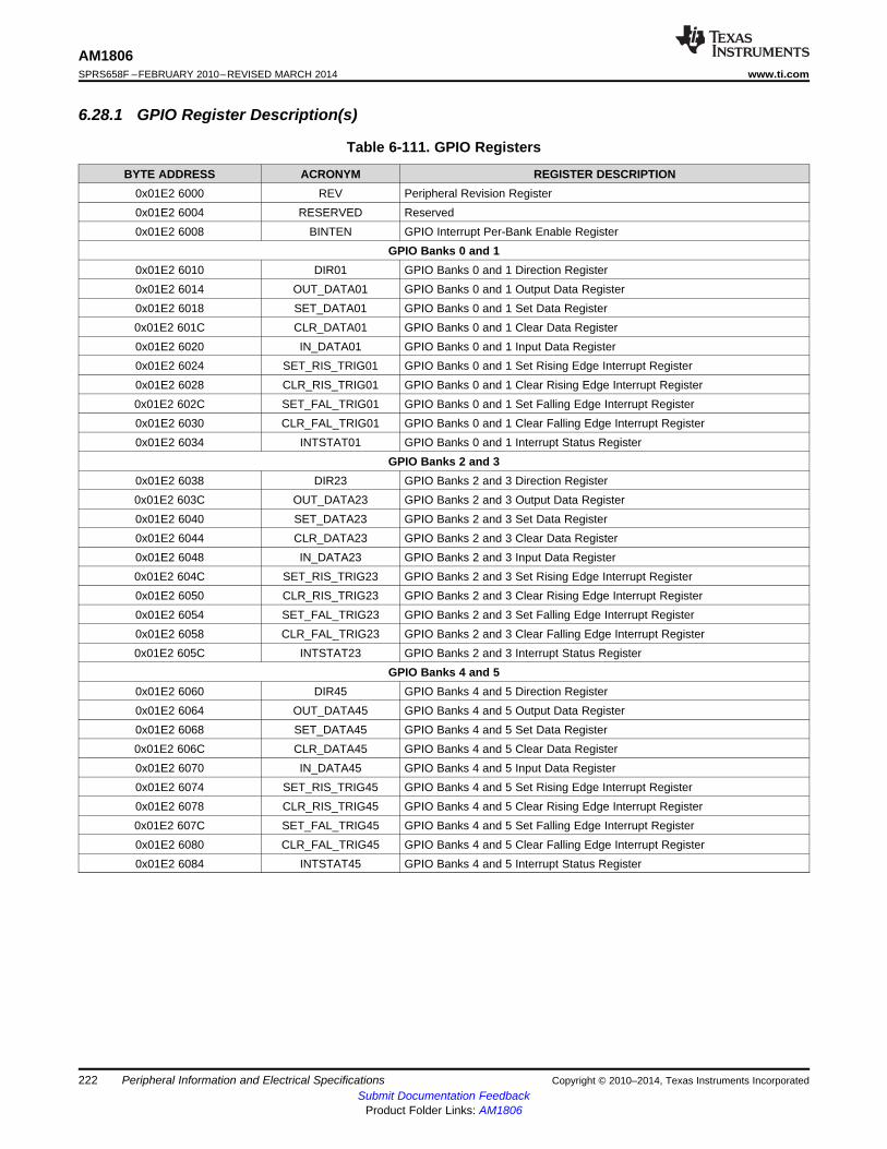
AM1806SPRS658F –FEBRUARY 2010–REVISED MARCH 2014 www.ti.com
6.28.1 GPIO Register Description(s)
Table 6-111. GPIO Registers
BYTE ADDRESS ACRONYM REGISTER DESCRIPTION0x01E2 6000 REV Peripheral Revision Register0x01E2 6004 RESERVED Reserved0x01E2 6008 BINTEN GPIO Interrupt Per-Bank Enable Register
GPIO Banks 0 and 10x01E2 6010 DIR01 GPIO Banks 0 and 1 Direction Register0x01E2 6014 OUT_DATA01 GPIO Banks 0 and 1 Output Data Register0x01E2 6018 SET_DATA01 GPIO Banks 0 and 1 Set Data Register0x01E2 601C CLR_DATA01 GPIO Banks 0 and 1 Clear Data Register0x01E2 6020 IN_DATA01 GPIO Banks 0 and 1 Input Data Register0x01E2 6024 SET_RIS_TRIG01 GPIO Banks 0 and 1 Set Rising Edge Interrupt Register0x01E2 6028 CLR_RIS_TRIG01 GPIO Banks 0 and 1 Clear Rising Edge Interrupt Register0x01E2 602C SET_FAL_TRIG01 GPIO Banks 0 and 1 Set Falling Edge Interrupt Register0x01E2 6030 CLR_FAL_TRIG01 GPIO Banks 0 and 1 Clear Falling Edge Interrupt Register0x01E2 6034 INTSTAT01 GPIO Banks 0 and 1 Interrupt Status Register
GPIO Banks 2 and 30x01E2 6038 DIR23 GPIO Banks 2 and 3 Direction Register0x01E2 603C OUT_DATA23 GPIO Banks 2 and 3 Output Data Register0x01E2 6040 SET_DATA23 GPIO Banks 2 and 3 Set Data Register0x01E2 6044 CLR_DATA23 GPIO Banks 2 and 3 Clear Data Register0x01E2 6048 IN_DATA23 GPIO Banks 2 and 3 Input Data Register0x01E2 604C SET_RIS_TRIG23 GPIO Banks 2 and 3 Set Rising Edge Interrupt Register0x01E2 6050 CLR_RIS_TRIG23 GPIO Banks 2 and 3 Clear Rising Edge Interrupt Register0x01E2 6054 SET_FAL_TRIG23 GPIO Banks 2 and 3 Set Falling Edge Interrupt Register0x01E2 6058 CLR_FAL_TRIG23 GPIO Banks 2 and 3 Clear Falling Edge Interrupt Register0x01E2 605C INTSTAT23 GPIO Banks 2 and 3 Interrupt Status Register
GPIO Banks 4 and 50x01E2 6060 DIR45 GPIO Banks 4 and 5 Direction Register0x01E2 6064 OUT_DATA45 GPIO Banks 4 and 5 Output Data Register0x01E2 6068 SET_DATA45 GPIO Banks 4 and 5 Set Data Register0x01E2 606C CLR_DATA45 GPIO Banks 4 and 5 Clear Data Register0x01E2 6070 IN_DATA45 GPIO Banks 4 and 5 Input Data Register0x01E2 6074 SET_RIS_TRIG45 GPIO Banks 4 and 5 Set Rising Edge Interrupt Register0x01E2 6078 CLR_RIS_TRIG45 GPIO Banks 4 and 5 Clear Rising Edge Interrupt Register0x01E2 607C SET_FAL_TRIG45 GPIO Banks 4 and 5 Set Falling Edge Interrupt Register0x01E2 6080 CLR_FAL_TRIG45 GPIO Banks 4 and 5 Clear Falling Edge Interrupt Register0x01E2 6084 INTSTAT45 GPIO Banks 4 and 5 Interrupt Status Register
222 Peripheral Information and Electrical Specifications Copyright © 2010–2014, Texas Instruments IncorporatedSubmit Documentation Feedback
Product Folder Links: AM1806
AM1806www.ti.com SPRS658F –FEBRUARY 2010–REVISED MARCH 2014
Table 6-111. GPIO Registers (continued)BYTE ADDRESS ACRONYM REGISTER DESCRIPTION
GPIO Banks 6 and 70x01E2 6088 DIR67 GPIO Banks 6 and 7 Direction Register0x01E2 608C OUT_DATA67 GPIO Banks 6 and 7 Output Data Register0x01E2 6090 SET_DATA67 GPIO Banks 6 and 7 Set Data Register0x01E2 6094 CLR_DATA67 GPIO Banks 6 and 7 Clear Data Register0x01E2 6098 IN_DATA67 GPIO Banks 6 and 7 Input Data Register0x01E2 609C SET_RIS_TRIG67 GPIO Banks 6 and 7 Set Rising Edge Interrupt Register0x01E2 60A0 CLR_RIS_TRIG67 GPIO Banks 6 and 7 Clear Rising Edge Interrupt Register0x01E2 60A4 SET_FAL_TRIG67 GPIO Banks 6 and 7 Set Falling Edge Interrupt Register0x01E2 60A8 CLR_FAL_TRIG67 GPIO Banks 6 and 7 Clear Falling Edge Interrupt Register0x01E2 60AC INTSTAT67 GPIO Banks 6 and 7 Interrupt Status Register
GPIO Bank 80x01E2 60B0 DIR8 GPIO Bank 8 Direction Register0x01E2 60B4 OUT_DATA8 GPIO Bank 8 Output Data Register0x01E2 60B8 SET_DATA8 GPIO Bank 8 Set Data Register0x01E2 60BC CLR_DATA8 GPIO Bank 8 Clear Data Register0x01E2 60C0 IN_DATA8 GPIO Bank 8 Input Data Register0x01E2 60C4 SET_RIS_TRIG8 GPIO Bank 8 Set Rising Edge Interrupt Register0x01E2 60C8 CLR_RIS_TRIG8 GPIO Bank 8 Clear Rising Edge Interrupt Register0x01E2 60CC SET_FAL_TRIG8 GPIO Bank 8 Set Falling Edge Interrupt Register0x01E2 60D0 CLR_FAL_TRIG8 GPIO Bank 8 Clear Falling Edge Interrupt Register0x01E2 60D4 INTSTAT8 GPIO Bank 8 Interrupt Status Register
Copyright © 2010–2014, Texas Instruments Incorporated Peripheral Information and Electrical Specifications 223Submit Documentation Feedback
Product Folder Links: AM1806
GP [ ]as input
n m
2
1
GP [ ]as input
n m
GPn m[ ]as output
4
3
2
1
AM1806SPRS658F –FEBRUARY 2010–REVISED MARCH 2014 www.ti.com
6.28.2 GPIO Peripheral Input/Output Electrical Data/Timing
Table 6-112. Timing Requirements for GPIO Inputs (1) (see Figure 6-76)1.3V, 1.2V, 1.1V, 1.0V
NO. UNITMIN MAX
1 tw(GPIH) Pulse duration, GPn[m] as input high 2C (1) (2) ns2 tw(GPIL) Pulse duration, GPn[m] as input low 2C (1) (2) ns
(1) The pulse width given is sufficient to generate a CPU interrupt or an EDMA event. However, if a user wants to have the devicerecognize the GPIx changes through software polling of the GPIO register, the GPIx duration must be extended to allow the deviceenough time to access the GPIO register through the internal bus.
(2) C=SYSCLK4 period in ns.
Table 6-113. Switching Characteristics Over Recommended Operating Conditions for GPIO Outputs(see Figure 6-76)
1.3V, 1.2V, 1.1V, 1.0VNO. PARAMETER UNIT
MIN MAX3 tw(GPOH) Pulse duration, GPn[m] as output high 2C (1) (2) ns4 tw(GPOL) Pulse duration, GPn[m] as output low 2C (1) (2) ns
(1) This parameter value should not be used as a maximum performance specification. Actual performance of back-to-back accesses of theGPIO is dependent upon internal bus activity.
(2) C=SYSCLK4 period in ns.
Figure 6-76. GPIO Port Timing
6.28.3 GPIO Peripheral External Interrupts Electrical Data/Timing
Table 6-114. Timing Requirements for External Interrupts (1) (see Figure 6-77)1.3V, 1.2V, 1.1V,
1.0VNO. UNITMIN MAX
1 tw(ILOW) Width of the external interrupt pulse low 2C (1) (2) ns2 tw(IHIGH) Width of the external interrupt pulse high 2C (1) (2) ns
(1) The pulse width given is sufficient to generate an interrupt or an EDMA event. However, if a user wants to have the device recognize theGPIO changes through software polling of the GPIO register, the GPIO duration must be extended to allow the device enough time toaccess the GPIO register through the internal bus.
(2) C=SYSCLK4 period in ns.
Figure 6-77. GPIO External Interrupt Timing
224 Peripheral Information and Electrical Specifications Copyright © 2010–2014, Texas Instruments IncorporatedSubmit Documentation Feedback
Product Folder Links: AM1806
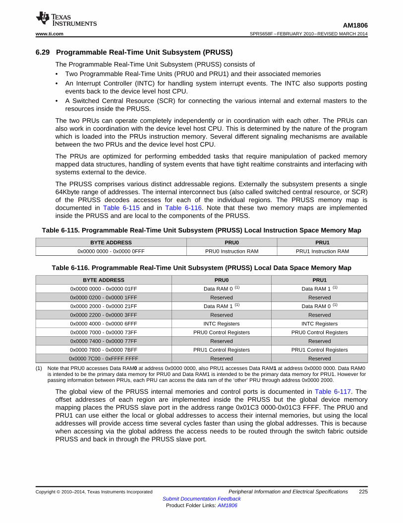
AM1806www.ti.com SPRS658F –FEBRUARY 2010–REVISED MARCH 2014
6.29 Programmable Real-Time Unit Subsystem (PRUSS)The Programmable Real-Time Unit Subsystem (PRUSS) consists of• Two Programmable Real-Time Units (PRU0 and PRU1) and their associated memories• An Interrupt Controller (INTC) for handling system interrupt events. The INTC also supports posting
events back to the device level host CPU.• A Switched Central Resource (SCR) for connecting the various internal and external masters to the
resources inside the PRUSS.
The two PRUs can operate completely independently or in coordination with each other. The PRUs canalso work in coordination with the device level host CPU. This is determined by the nature of the programwhich is loaded into the PRUs instruction memory. Several different signaling mechanisms are availablebetween the two PRUs and the device level host CPU.
The PRUs are optimized for performing embedded tasks that require manipulation of packed memorymapped data structures, handling of system events that have tight realtime constraints and interfacing withsystems external to the device.
The PRUSS comprises various distinct addressable regions. Externally the subsystem presents a single64Kbyte range of addresses. The internal interconnect bus (also called switched central resource, or SCR)of the PRUSS decodes accesses for each of the individual regions. The PRUSS memory map isdocumented in Table 6-115 and in Table 6-116. Note that these two memory maps are implementedinside the PRUSS and are local to the components of the PRUSS.
Table 6-115. Programmable Real-Time Unit Subsystem (PRUSS) Local Instruction Space Memory Map
BYTE ADDRESS PRU0 PRU10x0000 0000 - 0x0000 0FFF PRU0 Instruction RAM PRU1 Instruction RAM
Table 6-116. Programmable Real-Time Unit Subsystem (PRUSS) Local Data Space Memory Map
BYTE ADDRESS PRU0 PRU10x0000 0000 - 0x0000 01FF Data RAM 0 (1) Data RAM 1 (1)
0x0000 0200 - 0x0000 1FFF Reserved Reserved0x0000 2000 - 0x0000 21FF Data RAM 1 (1) Data RAM 0 (1)
0x0000 2200 - 0x0000 3FFF Reserved Reserved0x0000 4000 - 0x0000 6FFF INTC Registers INTC Registers0x0000 7000 - 0x0000 73FF PRU0 Control Registers PRU0 Control Registers0x0000 7400 - 0x0000 77FF Reserved Reserved0x0000 7800 - 0x0000 7BFF PRU1 Control Registers PRU1 Control Registers0x0000 7C00 - 0xFFFF FFFF Reserved Reserved
(1) Note that PRU0 accesses Data RAM0 at address 0x0000 0000, also PRU1 accesses Data RAM1 at address 0x0000 0000. Data RAM0is intended to be the primary data memory for PRU0 and Data RAM1 is intended to be the primary data memory for PRU1. However forpassing information between PRUs, each PRU can access the data ram of the ‘other’ PRU through address 0x0000 2000.
The global view of the PRUSS internal memories and control ports is documented in Table 6-117. Theoffset addresses of each region are implemented inside the PRUSS but the global device memorymapping places the PRUSS slave port in the address range 0x01C3 0000-0x01C3 FFFF. The PRU0 andPRU1 can use either the local or global addresses to access their internal memories, but using the localaddresses will provide access time several cycles faster than using the global addresses. This is becausewhen accessing via the global address the access needs to be routed through the switch fabric outsidePRUSS and back in through the PRUSS slave port.
Copyright © 2010–2014, Texas Instruments Incorporated Peripheral Information and Electrical Specifications 225Submit Documentation Feedback
Product Folder Links: AM1806
AM1806SPRS658F –FEBRUARY 2010–REVISED MARCH 2014 www.ti.com
Table 6-117. Programmable Real-Time Unit Subsystem (PRUSS) Global Memory Map
BYTE ADDRESS REGION0x01C3 0000 - 0x01C3 01FF Data RAM 00x01C3 0200 - 0x01C3 1FFF Reserved0x01C3 2000 - 0x01C3 21FF Data RAM 10x01C3 2200 - 0x01C3 3FFF Reserved0x01C3 4000 - 0x01C3 6FFF INTC Registers0x01C3 7000 - 0x01C3 73FF PRU0 Control Registers0x01C3 7400 - 0x01C3 77FF PRU0 Debug Registers0x01C3 7800 - 0x01C3 7BFF PRU1 Control Registers0x01C3 7C00 - 0x01C3 7FFF PRU1 Debug Registers0x01C3 8000 - 0x01C3 8FFF PRU0 Instruction RAM0x01C3 9000 - 0x01C3 BFFF Reserved0x01C3 C000 - 0x01C3 CFFF PRU1 Instruction RAM0x01C3 D000 - 0x01C3 FFFF Reserved
Each of the PRUs can access the rest of the device memory (including memory mapped peripheral andconfiguration registers) using the global memory space addresses
6.29.1 PRUSS Register Descriptions
Table 6-118. Programmable Real-Time Unit Subsystem (PRUSS) Control / Status Registers
PRU0 BYTE ADDRESS PRU1 BYTE ADDRESS ACRONYM REGISTER DESCRIPTION0x01C3 7000 0x01C3 7800 CONTROL PRU Control Register0x01C3 7004 0x01C3 7804 STATUS PRU Status Register0x01C3 7008 0x01C3 7808 WAKEUP PRU Wakeup Enable Register0x01C3 700C 0x01C3 780C CYCLCNT PRU Cycle Count0x01C3 7010 0x01C3 7810 STALLCNT PRU Stall Count
PRU Constant Table Block Index0x01C3 7020 0x01C3 7820 CONTABBLKIDX0 Register 0PRU Constant Table Programmable0x01C3 7028 0x01C3 7828 CONTABPROPTR0 Pointer Register 0PRU Constant Table Programmable0x01C3 702C 0x01C3 782C CONTABPROPTR1 Pointer Register 1PRU Internal General Purpose0x01C37400 - 0x01C3747C 0x01C3 7C00 - 0x01C3 7C7C INTGPR0 – INTGPR31 Register 0 (for Debug)PRU Internal General Purpose0x01C37480 - 0x01C374FC 0x01C3 7C80 - 0x01C3 7CFC INTCTER0 – INTCTER31 Register 0 (for Debug)
Table 6-119. Programmable Real-Time Unit Subsystem Interrupt Controller (PRUSS INTC) Registers
BYTE ADDRESS ACRONYM REGISTER DESCRIPTION0x01C3 4000 REVID Revision ID Register0x01C3 4004 CONTROL Control Register0x01C3 4010 GLBLEN Global Enable Register0x01C3 401C GLBLNSTLVL Global Nesting Level Register0x01C3 4020 STATIDXSET System Interrupt Status Indexed Set Register0x01C3 4024 STATIDXCLR System Interrupt Status Indexed Clear Register0x01C3 4028 ENIDXSET System Interrupt Enable Indexed Set Register0x01C3 402C ENIDXCLR System Interrupt Enable Indexed Clear Register0x01C3 4034 HSTINTENIDXSET Host Interrupt Enable Indexed Set Register0x01C3 4038 HSTINTENIDXCLR Host Interrupt Enable Indexed Clear Register
226 Peripheral Information and Electrical Specifications Copyright © 2010–2014, Texas Instruments IncorporatedSubmit Documentation Feedback
Product Folder Links: AM1806
AM1806www.ti.com SPRS658F –FEBRUARY 2010–REVISED MARCH 2014
Table 6-119. Programmable Real-Time Unit Subsystem Interrupt Controller (PRUSS INTC)Registers (continued)
BYTE ADDRESS ACRONYM REGISTER DESCRIPTION0x01C3 4080 GLBLPRIIDX Global Prioritized Index Register0x01C3 4200 STATSETINT0 System Interrupt Status Raw/Set Register 00x01C3 4204 STATSETINT1 System Interrupt Status Raw/Set Register 10x01C3 4280 STATCLRINT0 System Interrupt Status Enabled/Clear Register 00x01C3 4284 STATCLRINT1 System Interrupt Status Enabled/Clear Register 10x01C3 4300 ENABLESET0 System Interrupt Enable Set Register 00x01C3 4304 ENABLESET1 System Interrupt Enable Set Register 10x01C3 4380 ENABLECLR0 System Interrupt Enable Clear Register 00x01C3 4384 ENABLECLR1 System Interrupt Enable Clear Register 1
0x01C3 4400 - 0x01C3 4440 CHANMAP0 - CHANMAP15 Channel Map Registers 0-150x01C3 4800 - 0x01C3 4808 HOSTMAP0 - HOSTMAP2 Host Map Register 0-2
HOSTINTPRIIDX0 -0x01C3 4900 - 0x01C3 4928 Host Interrupt Prioritized Index Registers 0-9HOSTINTPRIIDX90x01C3 4D00 POLARITY0 System Interrupt Polarity Register 00x01C3 4D04 POLARITY1 System Interrupt Polarity Register 10x01C3 4D80 TYPE0 System Interrupt Type Register 00x01C3 4D84 TYPE1 System Interrupt Type Register 1
HOSTINTNSTLVL0-0x01C3 5100 - 0x01C3 5128 Host Interrupt Nesting Level Registers 0-9HOSTINTNSTLVL90x01C3 5500 HOSTINTEN Host Interrupt Enable Register
Copyright © 2010–2014, Texas Instruments Incorporated Peripheral Information and Electrical Specifications 227Submit Documentation Feedback
Product Folder Links: AM1806
AM1806SPRS658F –FEBRUARY 2010–REVISED MARCH 2014 www.ti.com
6.30 Emulation LogicThis section describes the steps to use a third party debugger on the ARM926EJ-S within the device. Thedebug capabilities and features for ARM are as shown below.
ARM:• Basic Debug
– Execution Control– System Visibility
• Advanced Debug– Global Start– Global Stop
• Advanced System Control– Subsystem reset via debug– Peripheral notification of debug events– Cache-coherent debug accesses
• Program Trace– Program flow corruption– Code coverage– Path coverage– Thread/interrupt synchronization problems
• Data Trace– Memory corruption
• Timing Trace– Profiling
• Analysis Actions– Stop program execution– Control trace streams– Generate debug interrupt– Benchmarking with counters– External trigger generation– Debug state machine state transition– Combinational and Sequential event generation
• Analysis Events– Program event detection– Data event detection– External trigger Detection– System event detection (i.e. cache miss)– Debug state machine state detection
• Analysis Configuration– Application access– Debugger access
228 Peripheral Information and Electrical Specifications Copyright © 2010–2014, Texas Instruments IncorporatedSubmit Documentation Feedback
Product Folder Links: AM1806
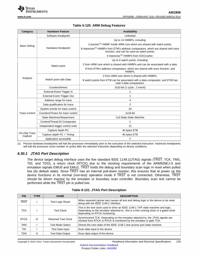
AM1806www.ti.com SPRS658F –FEBRUARY 2010–REVISED MARCH 2014
Table 6-120. ARM Debug Features
Category Hardware Feature AvailabilitySoftware breakpoint Unlimited
Up to 14 HWBPs, including:2 precise (1) HWBP inside ARM core which are shared with watch points.Basic Debug
Hardware breakpoint 8 imprecise (1) HWBPs from ETM’s address comparators, which are shared with tracefunction, and can be used as watch points.4 imprecise (1) HWBPs from ICECrusher.
Up to 6 watch points, including:2 from ARM core which is shared with HWBPs and can be associated with a data.Watch point
8 from ETM’s address comparators, which are shared with trace function, andHWBPs.
2 from ARM core which is shared with HWBPs.Analysis Watch point with Data 8 watch points from ETM can be associated with a data comparator, and ETM has
total 4 data comparators.Counters/timers 3x32-bit (1 cycle ; 2 event)
External Event Trigger In 1External Event Trigger Out 1
Address range for trace 4Data qualification for trace 2
System events for trace control 20Trace Control Counters/Timers for trace control 2x16-bit
State Machines/Sequencers 1x3-State State MachineContext/Thread ID Comparator 1
Independent trigger control units 12Capture depth PC 4k bytes ETB
On-chip Trace Capture depth PC + Timing 4k bytes ETBCaptureApplication accessible Y
(1) Precise hardware breakpoints will halt the processor immediately prior to the execution of the selected instruction. Imprecise breakpointswill halt the processor some number of cycles after the selected instruction depending on device conditions.
6.30.1 JTAG Port DescriptionThe device target debug interface uses the five standard IEEE 1149.1(JTAG) signals (TRST, TCK, TMS,TDI, and TDO), a return clock (RTCK) due to the clocking requirements of the ARM926EJ-S andemulation signals EMU0 and EMU1. TRST holds the debug and boundary scan logic in reset when pulledlow (its default state). Since TRST has an internal pull-down resistor, this ensures that at power up thedevice functions in its normal (non-test) operation mode if TRST is not connected. Otherwise, TRSTshould be driven inactive by the emulator or boundary scan controller. Boundary scan test cannot beperformed while the TRST pin is pulled low.
Table 6-121. JTAG Port Description
PIN TYPE NAME DESCRIPTIONWhen asserted (active low) causes all test and debug logic in the device to be resetTRST I Test Logic Reset along with the IEEE 1149.1 interfaceThis is the test clock used to drive an IEEE 1149.1 TAP state machine and logic.
TCK I Test Clock Depending on the emulator attached to , this is a free running clock or a gated clockdepending on RTCK monitoring.Synchronized TCK. Depending on the emulator attached to, the JTAG signals areRTCK O Returned Test Clock clocked from RTCK or RTCK is monitored by the emulator to gate TCK.
TMS I Test Mode Select Directs the next state of the IEEE 1149.1 test access port state machineTDI I Test Data Input Scan data input to the deviceTDO O Test Data Output Scan data output of the device
Copyright © 2010–2014, Texas Instruments Incorporated Peripheral Information and Electrical Specifications 229Submit Documentation Feedback
Product Folder Links: AM1806
TDO Router
TDI
StepsCLK
TMS
Router ARM926EJ-S/ETM
AM1806SPRS658F –FEBRUARY 2010–REVISED MARCH 2014 www.ti.com
Table 6-121. JTAG Port Description (continued)PIN TYPE NAME DESCRIPTION
EMU0 I/O Emulation 0 Channel 0 trigger + HSRTDXEMU1 I/O Emulation 1 Channel 1 trigger + HSRTDX
6.30.2 Scan Chain Configuration ParametersTable 6-122 shows the TAP configuration details required to configure the router/emulator for this device.
Table 6-122. JTAG Port Description
Router Port ID Default TAP TAP Name Tap IR Length17 No Reserved 3818 No ARM926 419 No ETB 4
The router is revision C and has a 6-bit IR length.
6.30.3 Initial Scan Chain ConfigurationThe first level of debug interface that sees the scan controller is the TAP router module. The debuggercan configure the TAP router for serially linking up to 16 TAP controllers or individually scanning one ofthe TAP controllers without disrupting the IR state of the other TAPs.
6.30.3.1 Adding TAPS to the Scan Chain
The TAP router must be programmed to add additional TAPs to the scan chain. The following JTAG scansmust be completed to add the ARM926EJ-S to the scan chain.
A Power-On Reset (POR) or the JTAG Test-Logic Reset state configures the TAP router to contain onlythe router’s TAP.
Figure 6-78. Adding ARM926EJ-S to the scan chain
Pre-amble: The device whose data reaches the emulator first is listed first in the board configuration file.This device is a pre-amble for all the other devices. This device has the lowest device ID.
Post-amble: The device whose data reaches the emulator last is listed last in the board configuration file.This device is a post-amble for all the other devices. This device has the highest device ID.
230 Peripheral Information and Electrical Specifications Copyright © 2010–2014, Texas Instruments IncorporatedSubmit Documentation Feedback
Product Folder Links: AM1806
AM1806www.ti.com SPRS658F –FEBRUARY 2010–REVISED MARCH 2014
• Function : Update the JTAG preamble and post-amble counts.– Parameter : The IR pre-amble count is '0'.– Parameter : The IR post-amble count is '0'.– Parameter : The DR pre-amble count is '0'.– Parameter : The DR post-amble count is '0'.– Parameter : The IR main count is '6'.– Parameter : The DR main count is '1'.
• Function : Do a send-only JTAG IR/DR scan.– Parameter : The route to JTAG shift state is 'shortest transition'.– Parameter : The JTAG shift state is 'shift-ir'.– Parameter : The JTAG destination state is 'pause-ir'.– Parameter : The bit length of the command is '6'.– Parameter : The send data value is '0x00000007'.– Parameter : The actual receive data is 'discarded'.
• Function : Do a send-only JTAG IR/DR scan.– Parameter : The route to JTAG shift state is 'shortest transition'.– Parameter : The JTAG shift state is 'shift-dr'.– Parameter : The JTAG destination state is 'pause-dr'.– Parameter : The bit length of the command is '8'.– Parameter : The send data value is '0x00000089'.– Parameter : The actual receive data is 'discarded'.
• Function : Do a send-only JTAG IR/DR scan.– Parameter : The route to JTAG shift state is 'shortest transition'.– Parameter : The JTAG shift state is 'shift-ir'.– Parameter : The JTAG destination state is 'pause-ir'.– Parameter : The bit length of the command is '6'.– Parameter : The send data value is '0x00000002'.– Parameter : The actual receive data is 'discarded'.
• Function : Embed the port address in next command.– Parameter : The port address field is '0x0f000000'.– Parameter : The port address value is '3'.
• Function : Do a send-only JTAG IR/DR scan.– Parameter : The route to JTAG shift state is 'shortest transition'.– Parameter : The JTAG shift state is 'shift-dr'.– Parameter : The JTAG destination state is 'pause-dr'.– Parameter : The bit length of the command is '32'.– Parameter : The send data value is '0xa2002108'.– Parameter : The actual receive data is 'discarded'.
• Function : Do a send-only all-ones JTAG IR/DR scan.– Parameter : The JTAG shift state is 'shift-ir'.– Parameter : The JTAG destination state is 'run-test/idle'.– Parameter : The bit length of the command is '6'.– Parameter : The send data value is 'all-ones'.– Parameter : The actual receive data is 'discarded'.
• Function : Wait for a minimum number of TCLK pulses.– Parameter : The count of TCLK pulses is '10'.
Copyright © 2010–2014, Texas Instruments Incorporated Peripheral Information and Electrical Specifications 231Submit Documentation Feedback
Product Folder Links: AM1806
TDI Router ARM926EJ-S/ETM
TDO
StepsCLK
TMS
Router ARM926EJ-S/ETM ETB
AM1806SPRS658F –FEBRUARY 2010–REVISED MARCH 2014 www.ti.com
• Function : Update the JTAG preamble and post-amble counts.– Parameter : The IR pre-amble count is '0'.– Parameter : The IR post-amble count is '6'.– Parameter : The DR pre-amble count is '0'.– Parameter : The DR post-amble count is '1'.– Parameter : The IR main count is '4'.– Parameter : The DR main count is '1'.
The initial scan chain contains only the TAP router module. The following steps must be completed inorder to add ETB TAP to the scan chain.
Figure 6-79. Adding ETB to the scan chain• Function : Do a send-only JTAG IR/DR scan.
– Parameter : The route to JTAG shift state is 'shortest transition'.– Parameter : The JTAG shift state is 'shift-ir'.– Parameter : The JTAG destination state is 'pause-ir'.– Parameter : The bit length of the command is '6'.– Parameter : The send data value is '0x00000007'.– Parameter : The actual receive data is 'discarded'.
• Function : Do a send-only JTAG IR/DR scan.– Parameter : The route to JTAG shift state is 'shortest transition'.– Parameter : The JTAG shift state is 'shift-dr'.– Parameter : The JTAG destination state is 'pause-dr'.– Parameter : The bit length of the command is '8'.– Parameter : The send data value is '0x00000089'.– Parameter : The actual receive data is 'discarded'.
• Function : Do a send-only JTAG IR/DR scan.– Parameter : The route to JTAG shift state is 'shortest transition'.– Parameter : The JTAG shift state is 'shift-ir'.– Parameter : The JTAG destination state is 'pause-ir'.– Parameter : The bit length of the command is '6'.– Parameter : The send data value is '0x00000002'.– Parameter : The actual receive data is 'discarded'.
• Function : Embed the port address in next command.– Parameter : The port address field is '0x0f000000'.– Parameter : The port address value is '3'.
232 Peripheral Information and Electrical Specifications Copyright © 2010–2014, Texas Instruments IncorporatedSubmit Documentation Feedback
Product Folder Links: AM1806
AM1806www.ti.com SPRS658F –FEBRUARY 2010–REVISED MARCH 2014
• Function : Do a send-only JTAG IR/DR scan.– Parameter : The route to JTAG shift state is 'shortest transition'.– Parameter : The JTAG shift state is 'shift-dr'.– Parameter : The JTAG destination state is 'pause-dr'.– Parameter : The bit length of the command is '32'.– Parameter : The send data value is '0xa3302108'.– Parameter : The actual receive data is 'discarded'.
• Function : Do a send-only all-ones JTAG IR/DR scan.– Parameter : The JTAG shift state is 'shift-ir'.– Parameter : The JTAG destination state is 'run-test/idle'.– Parameter : The bit length of the command is '6'.– Parameter : The send data value is 'all-ones'.– Parameter : The actual receive data is 'discarded'.
• Function : Wait for a minimum number of TCLK pulses.– Parameter : The count of TCLK pulses is '10'.
• Function : Update the JTAG preamble and post-amble counts.– Parameter : The IR pre-amble count is '0'.– Parameter : The IR post-amble count is '6 + 4'.– Parameter : The DR pre-amble count is '0'.– Parameter : The DR post-amble count is '1 + 1'.– Parameter : The IR main count is '4'.– Parameter : The DR main count is '1'.
Copyright © 2010–2014, Texas Instruments Incorporated Peripheral Information and Electrical Specifications 233Submit Documentation Feedback
Product Folder Links: AM1806
AM1806SPRS658F –FEBRUARY 2010–REVISED MARCH 2014 www.ti.com
6.30.4 IEEE 1149.1 JTAGThe JTAG (1) interface is used for BSDL testing and emulation of the device.
The device requires that both TRST and RESET be asserted upon power up to be properly initialized.While RESET initializes the device, TRST initializes the device's emulation logic. Both resets are requiredfor proper operation.
While both TRST and RESET need to be asserted upon power up, only RESET needs to be released forthe device to boot properly. TRST may be asserted indefinitely for normal operation, keeping the JTAGport interface and device's emulation logic in the reset state.
TRST only needs to be released when it is necessary to use a JTAG controller to debug the device orexercise the device's boundary scan functionality. Note: TRST is synchronous and must be clocked byTCK; otherwise, the boundary scan logic may not respond as expected after TRST is asserted.
RESET must be released only in order for boundary-scan JTAG to read the variant field of IDCODEcorrectly. Other boundary-scan instructions work correctly independent of current state of RESET.
For maximum reliability, the device includes an internal pulldown (IPD) on the TRST pin to ensure thatTRST will always be asserted upon power up and the device's internal emulation logic will always beproperly initialized.
JTAG controllers from Texas Instruments actively drive TRST high. However, some third-party JTAGcontrollers may not drive TRST high but expect the use of a pullup resistor on TRST.
When using this type of JTAG controller, assert TRST to initialize the device after powerup and externallydrive TRST high before attempting any emulation or boundary scan operations.
6.30.4.1 JTAG Peripheral Register Description(s) – JTAG ID Register (DEVIDR0)
Table 6-123. DEVIDR0 Register
BYTE ADDRESS ACRONYM REGISTER DESCRIPTION COMMENTSRead-only. Provides 32-bit0x01C1 4018 DEVIDR0 JTAG Identification Register JTAG ID of the device.
(1) IEEE Standard 1149.1-1990 Standard-Test-Access Port and Boundary Scan Architecture.
The JTAG ID register is a read-only register that identifies to the customer the JTAG/Device ID. For thedevice, the JTAG ID register resides at address location 0x01C1 4018. The register hex value for eachsilicon revision is:• 0x0B7D 102F for silicon revision 1.0• 0x0B7D 102F for silicon revision 1.1• 0x1B7D 102F for silicon revision 2.0For the actual register bit names and their associated bit field descriptions, see Figure 6-80 and Table 6-124.
Figure 6-80. JTAG ID (DEVIDR0) Register Description - Register Value31-28 27-12 11-1 0
VARIANT (4-Bit) PART NUMBER (16-Bit) MANUFACTURER (11-Bit) LSBR-xxxx R-1011 0111 1101 0001 R-0000 0010 111 R-1
LEGEND: R = Read, W = Write, n = value at reset
234 Peripheral Information and Electrical Specifications Copyright © 2010–2014, Texas Instruments IncorporatedSubmit Documentation Feedback
Product Folder Links: AM1806
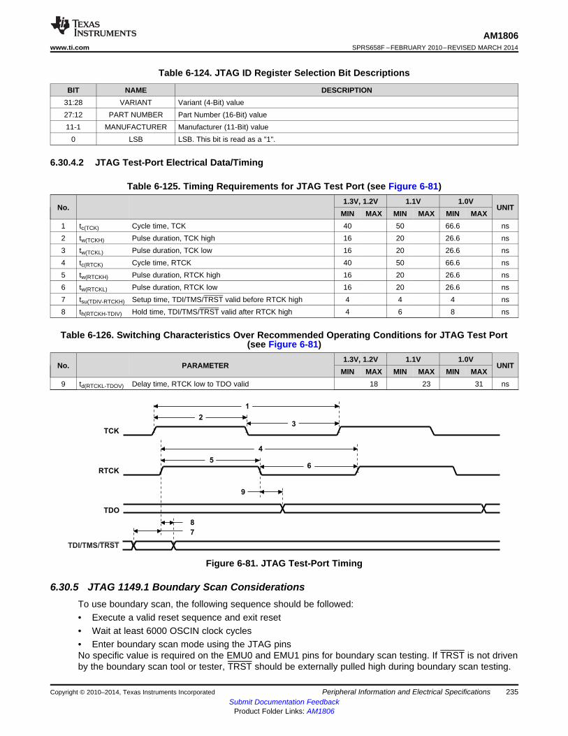
TCK
TDO
1
7
23
RTCK
4
56
9
8
TDI/TMS/TRST
AM1806www.ti.com SPRS658F –FEBRUARY 2010–REVISED MARCH 2014
Table 6-124. JTAG ID Register Selection Bit Descriptions
BIT NAME DESCRIPTION31:28 VARIANT Variant (4-Bit) value27:12 PART NUMBER Part Number (16-Bit) value11-1 MANUFACTURER Manufacturer (11-Bit) value
0 LSB LSB. This bit is read as a "1".
6.30.4.2 JTAG Test-Port Electrical Data/Timing
Table 6-125. Timing Requirements for JTAG Test Port (see Figure 6-81)1.3V, 1.2V 1.1V 1.0V
No. UNITMIN MAX MIN MAX MIN MAX
1 tc(TCK) Cycle time, TCK 40 50 66.6 ns2 tw(TCKH) Pulse duration, TCK high 16 20 26.6 ns3 tw(TCKL) Pulse duration, TCK low 16 20 26.6 ns4 tc(RTCK) Cycle time, RTCK 40 50 66.6 ns5 tw(RTCKH) Pulse duration, RTCK high 16 20 26.6 ns6 tw(RTCKL) Pulse duration, RTCK low 16 20 26.6 ns7 tsu(TDIV-RTCKH) Setup time, TDI/TMS/TRST valid before RTCK high 4 4 4 ns8 th(RTCKH-TDIV) Hold time, TDI/TMS/TRST valid after RTCK high 4 6 8 ns
Table 6-126. Switching Characteristics Over Recommended Operating Conditions for JTAG Test Port(see Figure 6-81)
1.3V, 1.2V 1.1V 1.0VNo. PARAMETER UNIT
MIN MAX MIN MAX MIN MAX9 td(RTCKL-TDOV) Delay time, RTCK low to TDO valid 18 23 31 ns
Figure 6-81. JTAG Test-Port Timing
6.30.5 JTAG 1149.1 Boundary Scan ConsiderationsTo use boundary scan, the following sequence should be followed:• Execute a valid reset sequence and exit reset• Wait at least 6000 OSCIN clock cycles• Enter boundary scan mode using the JTAG pinsNo specific value is required on the EMU0 and EMU1 pins for boundary scan testing. If TRST is not drivenby the boundary scan tool or tester, TRST should be externally pulled high during boundary scan testing.
Copyright © 2010–2014, Texas Instruments Incorporated Peripheral Information and Electrical Specifications 235Submit Documentation Feedback
Product Folder Links: AM1806
AM1806SPRS658F –FEBRUARY 2010–REVISED MARCH 2014 www.ti.com
7 Device and Documentation Support
7.1 Device Support
7.1.1 Development SupportTI offers an extensive line of development tools for the device platform, including tools to evaluate theperformance of the processors, generate code, develop algorithm implementations, and fully integrate anddebug software and hardware modules. The tool's support documentation is electronically available withinthe Code Composer Studio™ Integrated Development Environment (IDE).
The following products support development of the device applications:
Software Development Tools:Code Composer Studio™ Integrated Development Environment (IDE): including EditorC/C++/Assembly Code Generation, and Debug plus additional development tools
Hardware Development Tools:Extended Development System (XDS™) EmulatorFor a complete listing of development-support tools for the device, visit the Texas Instruments web siteon the Worldwide Web at www.ti.com uniform resource locator (URL). For information on pricing andavailability, contact the nearest TI field sales office or authorized distributor.
7.1.2 Device and Development-Support Tool NomenclatureTo designate the stages in the product development cycle, TI assigns prefixes to the part numbers of allAM1xxx processors and support tools. Each commercial AM1xxx platform member has one of threeprefixes: X, P, or null (no prefix). Texas Instruments recommends two of three possible prefix designatorsfor its support tools: TMDX and TMDS. These prefixes represent evolutionary stages of productdevelopment from engineering prototypes (TMDX) through fully qualified production devices/tools (TMDS).
Device development evolutionary flow:
X Experimental device that is not necessarily representative of the final device's electricalspecifications.
P Final silicon die that conforms to the device's electrical specifications but has not completedquality and reliability verification.
NULL Fully-qualified production device.
Support tool development evolutionary flow:
TMDX Development-support product that has not yet completed Texas Instruments internalqualification testing.
TMDS Fully qualified development-support product.
X and P devices and TMDX development-support tools are shipped against the following disclaimer:
"Developmental product is intended for internal evaluation purposes."
NULL devices and TMDS development-support tools have been characterized fully, and the quality andreliability of the device have been demonstrated fully. TI's standard warranty applies.
Predictions show that prototype devices (X or P) have a greater failure rate than the standard productiondevices. Texas Instruments recommends that these devices not be used in any production systembecause their expected end-use failure rate still is undefined. Only qualified production devices are to beused.
Figure 7-1 provides a legend for reading the complete device.
236 Device and Documentation Support Copyright © 2010–2014, Texas Instruments IncorporatedSubmit Documentation Feedback
Product Folder Links: AM1806
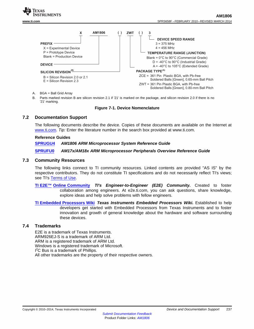
X AM1806 ( ) ZWT ( ) 3
PREFIX
X = Experimental Device
DEVICE
SILICON REVISION
3 = 375 MHz
Blank = 0°C to 90°C (Commercial Grade)
PACKAGE TYPE
361 Pin Plastic BGA, with Pb-freeSoldered Balls [Green], 0.65-mm Ball Pitch
ZCE =
DEVICE SPEED RANGE
TEMPERATURE RANGE (JUNCTION)
B = Silicon Revision 2.0 or 2.1E = Silicon Revision 2.3
D = -40°C to 90°C (Industrial Grade)
361 Pin Plastic BGA, with Pb-freeSoldered Balls [Green], 0.80-mm Ball Pitch
ZWT =
A = -40°C to 105°C (Extended Grade)
4 = 456 MHz
P = Prototype Device
Blank = Production Device
(B) (A)
AM1806www.ti.com SPRS658F –FEBRUARY 2010–REVISED MARCH 2014
A. BGA = Ball Grid ArrayB. Parts marked revision B are silicon revision 2.1 if '21' is marked on the package, and silicon revision 2.0 if there is no
'21' marking.
Figure 7-1. Device Nomenclature
7.2 Documentation SupportThe following documents describe the device. Copies of these documents are available on the Internet atwww.ti.com. Tip: Enter the literature number in the search box provided at www.ti.com.
Reference GuidesSPRUGU4 AM1806 ARM Microprocessor System Reference Guide
SPRUFU0 AM17x/AM18x ARM Microprocessor Peripherals Overview Reference Guide
7.3 Community ResourcesThe following links connect to TI community resources. Linked contents are provided "AS IS" by therespective contributors. They do not constitute TI specifications and do not necessarily reflect TI's views;see TI's Terms of Use.
TI E2E™ Online Community TI's Engineer-to-Engineer (E2E) Community. Created to fostercollaboration among engineers. At e2e.ti.com, you can ask questions, share knowledge,explore ideas and help solve problems with fellow engineers.
TI Embedded Processors Wiki Texas Instruments Embedded Processors Wiki. Established to helpdevelopers get started with Embedded Processors from Texas Instruments and to fosterinnovation and growth of general knowledge about the hardware and software surroundingthese devices.
7.4 TrademarksE2E is a trademark of Texas Instruments.ARM926EJ-S is a trademark of ARM Ltd.ARM is a registered trademark of ARM Ltd.Windows is a registered trademark of Microsoft.I2C Bus is a trademark of Phillips.All other trademarks are the property of their respective owners.
Copyright © 2010–2014, Texas Instruments Incorporated Device and Documentation Support 237Submit Documentation Feedback
Product Folder Links: AM1806
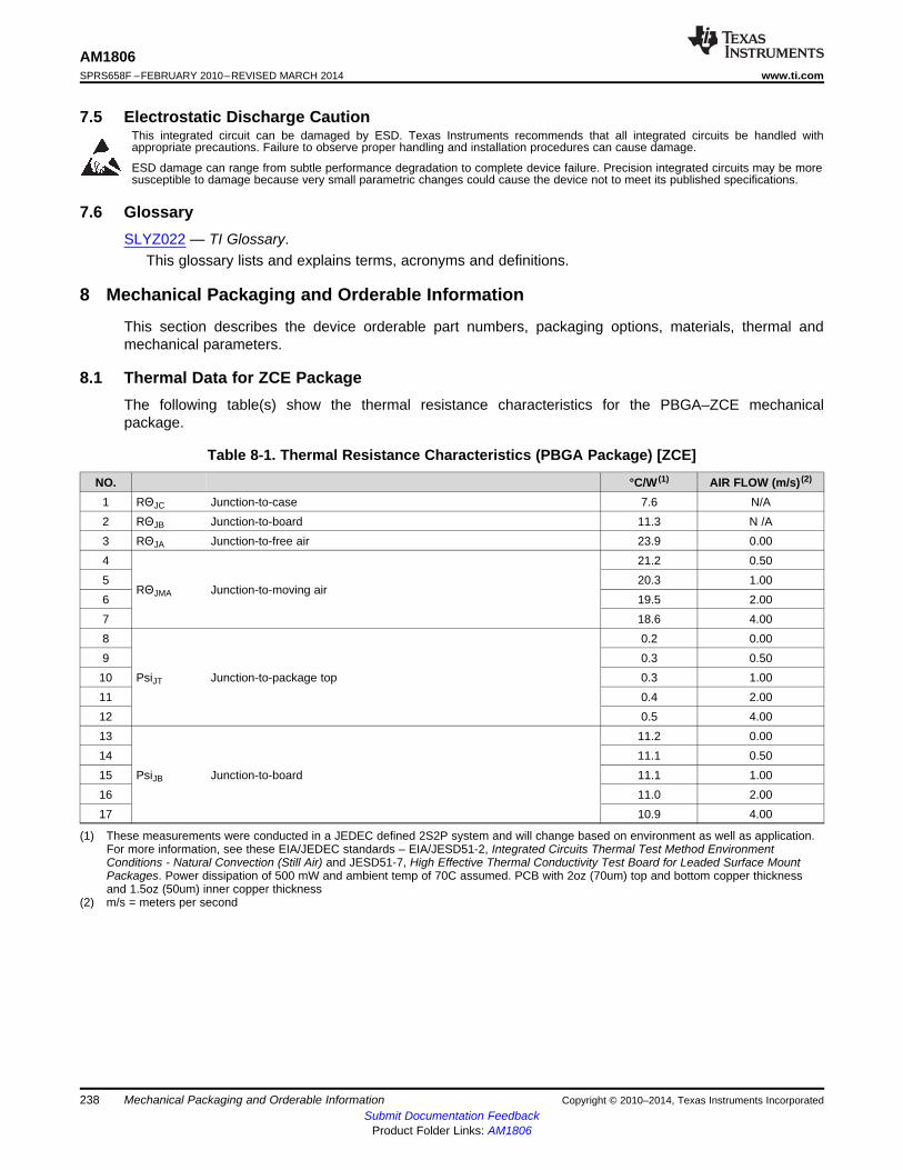
AM1806SPRS658F –FEBRUARY 2010–REVISED MARCH 2014 www.ti.com
7.5 Electrostatic Discharge CautionThis integrated circuit can be damaged by ESD. Texas Instruments recommends that all integrated circuits be handled withappropriate precautions. Failure to observe proper handling and installation procedures can cause damage.
ESD damage can range from subtle performance degradation to complete device failure. Precision integrated circuits may be moresusceptible to damage because very small parametric changes could cause the device not to meet its published specifications.
7.6 GlossarySLYZ022 — TI Glossary.
This glossary lists and explains terms, acronyms and definitions.
8 Mechanical Packaging and Orderable Information
This section describes the device orderable part numbers, packaging options, materials, thermal andmechanical parameters.
8.1 Thermal Data for ZCE PackageThe following table(s) show the thermal resistance characteristics for the PBGA–ZCE mechanicalpackage.
Table 8-1. Thermal Resistance Characteristics (PBGA Package) [ZCE]
NO. °C/W (1) AIR FLOW (m/s) (2)
1 RΘJC Junction-to-case 7.6 N/A2 RΘJB Junction-to-board 11.3 N /A3 RΘJA Junction-to-free air 23.9 0.004 21.2 0.505 20.3 1.00
RΘJMA Junction-to-moving air6 19.5 2.007 18.6 4.008 0.2 0.009 0.3 0.50
10 PsiJT Junction-to-package top 0.3 1.0011 0.4 2.0012 0.5 4.0013 11.2 0.0014 11.1 0.5015 PsiJB Junction-to-board 11.1 1.0016 11.0 2.0017 10.9 4.00
(1) These measurements were conducted in a JEDEC defined 2S2P system and will change based on environment as well as application.For more information, see these EIA/JEDEC standards – EIA/JESD51-2, Integrated Circuits Thermal Test Method EnvironmentConditions - Natural Convection (Still Air) and JESD51-7, High Effective Thermal Conductivity Test Board for Leaded Surface MountPackages. Power dissipation of 500 mW and ambient temp of 70C assumed. PCB with 2oz (70um) top and bottom copper thicknessand 1.5oz (50um) inner copper thickness
(2) m/s = meters per second
238 Mechanical Packaging and Orderable Information Copyright © 2010–2014, Texas Instruments IncorporatedSubmit Documentation Feedback
Product Folder Links: AM1806
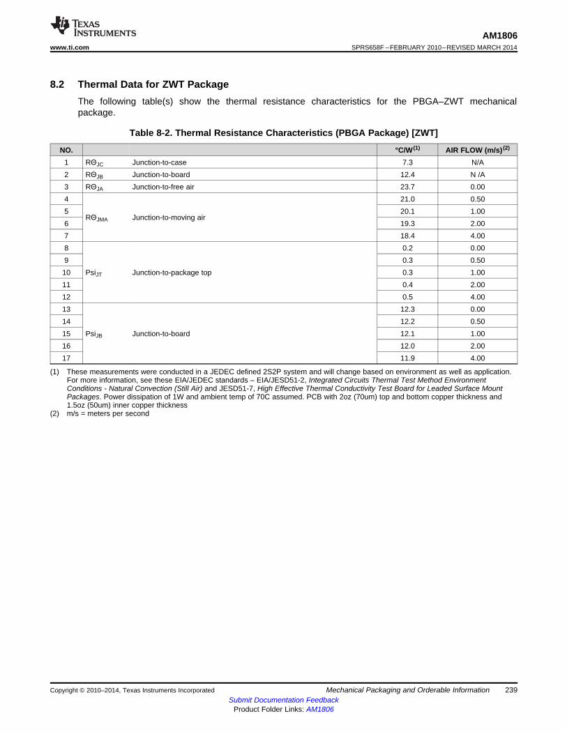
AM1806www.ti.com SPRS658F –FEBRUARY 2010–REVISED MARCH 2014
8.2 Thermal Data for ZWT PackageThe following table(s) show the thermal resistance characteristics for the PBGA–ZWT mechanicalpackage.
Table 8-2. Thermal Resistance Characteristics (PBGA Package) [ZWT]
NO. °C/W (1) AIR FLOW (m/s) (2)
1 RΘJC Junction-to-case 7.3 N/A2 RΘJB Junction-to-board 12.4 N /A3 RΘJA Junction-to-free air 23.7 0.004 21.0 0.505 20.1 1.00
RΘJMA Junction-to-moving air6 19.3 2.007 18.4 4.008 0.2 0.009 0.3 0.50
10 PsiJT Junction-to-package top 0.3 1.0011 0.4 2.0012 0.5 4.0013 12.3 0.0014 12.2 0.5015 PsiJB Junction-to-board 12.1 1.0016 12.0 2.0017 11.9 4.00
(1) These measurements were conducted in a JEDEC defined 2S2P system and will change based on environment as well as application.For more information, see these EIA/JEDEC standards – EIA/JESD51-2, Integrated Circuits Thermal Test Method EnvironmentConditions - Natural Convection (Still Air) and JESD51-7, High Effective Thermal Conductivity Test Board for Leaded Surface MountPackages. Power dissipation of 1W and ambient temp of 70C assumed. PCB with 2oz (70um) top and bottom copper thickness and1.5oz (50um) inner copper thickness
(2) m/s = meters per second
Copyright © 2010–2014, Texas Instruments Incorporated Mechanical Packaging and Orderable Information 239Submit Documentation Feedback
Product Folder Links: AM1806
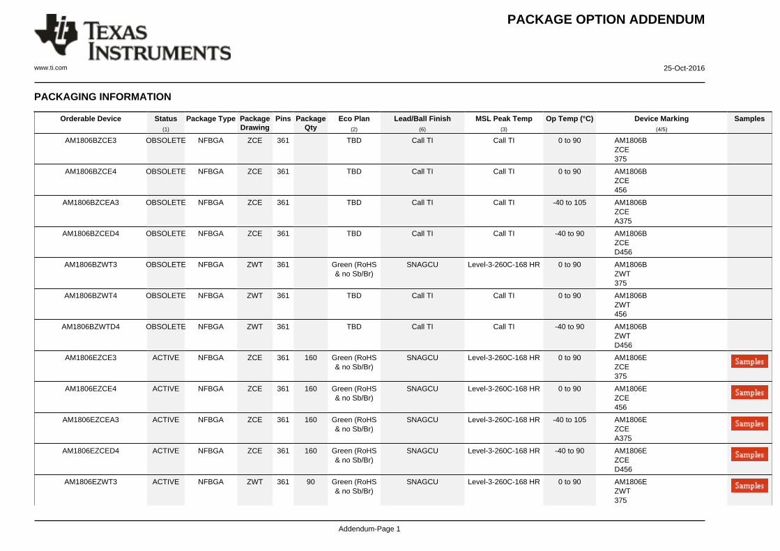
PACKAGE OPTION ADDENDUM
www.ti.com 25-Oct-2016
Addendum-Page 1
PACKAGING INFORMATION
Orderable Device Status(1)
Package Type PackageDrawing
Pins PackageQty
Eco Plan(2)
Lead/Ball Finish(6)
MSL Peak Temp(3)
Op Temp (°C) Device Marking(4/5)
Samples
AM1806BZCE3 OBSOLETE NFBGA ZCE 361 TBD Call TI Call TI 0 to 90 AM1806BZCE375
AM1806BZCE4 OBSOLETE NFBGA ZCE 361 TBD Call TI Call TI 0 to 90 AM1806BZCE456
AM1806BZCEA3 OBSOLETE NFBGA ZCE 361 TBD Call TI Call TI -40 to 105 AM1806BZCEA375
AM1806BZCED4 OBSOLETE NFBGA ZCE 361 TBD Call TI Call TI -40 to 90 AM1806BZCED456
AM1806BZWT3 OBSOLETE NFBGA ZWT 361 Green (RoHS& no Sb/Br)
SNAGCU Level-3-260C-168 HR 0 to 90 AM1806BZWT375
AM1806BZWT4 OBSOLETE NFBGA ZWT 361 TBD Call TI Call TI 0 to 90 AM1806BZWT456
AM1806BZWTD4 OBSOLETE NFBGA ZWT 361 TBD Call TI Call TI -40 to 90 AM1806BZWTD456
AM1806EZCE3 ACTIVE NFBGA ZCE 361 160 Green (RoHS& no Sb/Br)
SNAGCU Level-3-260C-168 HR 0 to 90 AM1806EZCE375
AM1806EZCE4 ACTIVE NFBGA ZCE 361 160 Green (RoHS& no Sb/Br)
SNAGCU Level-3-260C-168 HR 0 to 90 AM1806EZCE456
AM1806EZCEA3 ACTIVE NFBGA ZCE 361 160 Green (RoHS& no Sb/Br)
SNAGCU Level-3-260C-168 HR -40 to 105 AM1806EZCEA375
AM1806EZCED4 ACTIVE NFBGA ZCE 361 160 Green (RoHS& no Sb/Br)
SNAGCU Level-3-260C-168 HR -40 to 90 AM1806EZCED456
AM1806EZWT3 ACTIVE NFBGA ZWT 361 90 Green (RoHS& no Sb/Br)
SNAGCU Level-3-260C-168 HR 0 to 90 AM1806EZWT375
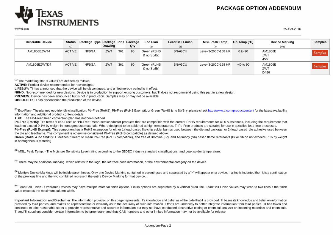
PACKAGE OPTION ADDENDUM
www.ti.com 25-Oct-2016
Addendum-Page 2
Orderable Device Status(1)
Package Type PackageDrawing
Pins PackageQty
Eco Plan(2)
Lead/Ball Finish(6)
MSL Peak Temp(3)
Op Temp (°C) Device Marking(4/5)
Samples
AM1806EZWT4 ACTIVE NFBGA ZWT 361 90 Green (RoHS& no Sb/Br)
SNAGCU Level-3-260C-168 HR 0 to 90 AM1806EZWT456
AM1806EZWTD4 ACTIVE NFBGA ZWT 361 90 Green (RoHS& no Sb/Br)
SNAGCU Level-3-260C-168 HR -40 to 90 AM1806EZWTD456
(1) The marketing status values are defined as follows:ACTIVE: Product device recommended for new designs.LIFEBUY: TI has announced that the device will be discontinued, and a lifetime-buy period is in effect.NRND: Not recommended for new designs. Device is in production to support existing customers, but TI does not recommend using this part in a new design.PREVIEW: Device has been announced but is not in production. Samples may or may not be available.OBSOLETE: TI has discontinued the production of the device.
(2) Eco Plan - The planned eco-friendly classification: Pb-Free (RoHS), Pb-Free (RoHS Exempt), or Green (RoHS & no Sb/Br) - please check http://www.ti.com/productcontent for the latest availabilityinformation and additional product content details.TBD: The Pb-Free/Green conversion plan has not been defined.Pb-Free (RoHS): TI's terms "Lead-Free" or "Pb-Free" mean semiconductor products that are compatible with the current RoHS requirements for all 6 substances, including the requirement thatlead not exceed 0.1% by weight in homogeneous materials. Where designed to be soldered at high temperatures, TI Pb-Free products are suitable for use in specified lead-free processes.Pb-Free (RoHS Exempt): This component has a RoHS exemption for either 1) lead-based flip-chip solder bumps used between the die and package, or 2) lead-based die adhesive used betweenthe die and leadframe. The component is otherwise considered Pb-Free (RoHS compatible) as defined above.Green (RoHS & no Sb/Br): TI defines "Green" to mean Pb-Free (RoHS compatible), and free of Bromine (Br) and Antimony (Sb) based flame retardants (Br or Sb do not exceed 0.1% by weightin homogeneous material)
(3) MSL, Peak Temp. - The Moisture Sensitivity Level rating according to the JEDEC industry standard classifications, and peak solder temperature.
(4) There may be additional marking, which relates to the logo, the lot trace code information, or the environmental category on the device.
(5) Multiple Device Markings will be inside parentheses. Only one Device Marking contained in parentheses and separated by a "~" will appear on a device. If a line is indented then it is a continuationof the previous line and the two combined represent the entire Device Marking for that device.
(6) Lead/Ball Finish - Orderable Devices may have multiple material finish options. Finish options are separated by a vertical ruled line. Lead/Ball Finish values may wrap to two lines if the finishvalue exceeds the maximum column width.
Important Information and Disclaimer:The information provided on this page represents TI's knowledge and belief as of the date that it is provided. TI bases its knowledge and belief on informationprovided by third parties, and makes no representation or warranty as to the accuracy of such information. Efforts are underway to better integrate information from third parties. TI has taken andcontinues to take reasonable steps to provide representative and accurate information but may not have conducted destructive testing or chemical analysis on incoming materials and chemicals.TI and TI suppliers consider certain information to be proprietary, and thus CAS numbers and other limited information may not be available for release.
PACKAGE OPTION ADDENDUM
www.ti.com 25-Oct-2016
Addendum-Page 3
In no event shall TI's liability arising out of such information exceed the total purchase price of the TI part(s) at issue in this document sold by TI to Customer on an annual basis.
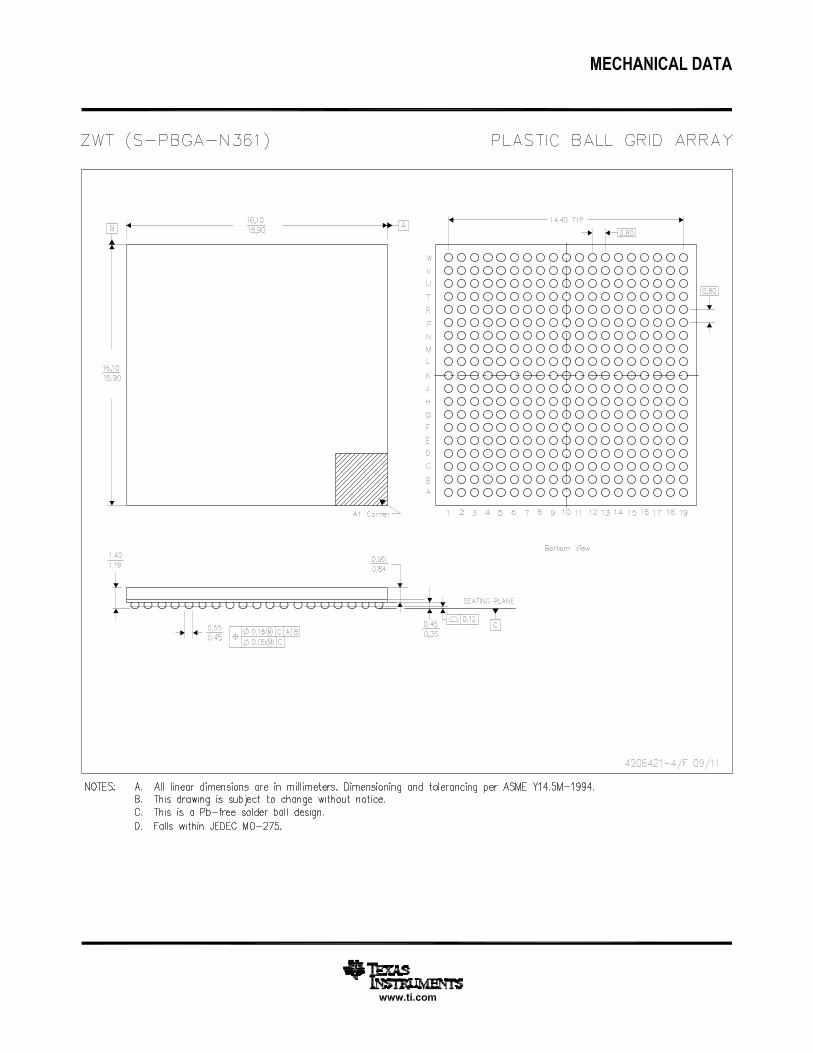
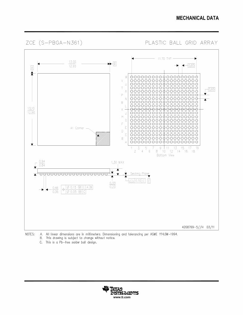

IMPORTANT NOTICE
Texas Instruments Incorporated and its subsidiaries (TI) reserve the right to make corrections, enhancements, improvements and otherchanges to its semiconductor products and services per JESD46, latest issue, and to discontinue any product or service per JESD48, latestissue. Buyers should obtain the latest relevant information before placing orders and should verify that such information is current andcomplete. All semiconductor products (also referred to herein as “components”) are sold subject to TI’s terms and conditions of salesupplied at the time of order acknowledgment.TI warrants performance of its components to the specifications applicable at the time of sale, in accordance with the warranty in TI’s termsand conditions of sale of semiconductor products. Testing and other quality control techniques are used to the extent TI deems necessaryto support this warranty. Except where mandated by applicable law, testing of all parameters of each component is not necessarilyperformed.TI assumes no liability for applications assistance or the design of Buyers’ products. Buyers are responsible for their products andapplications using TI components. To minimize the risks associated with Buyers’ products and applications, Buyers should provideadequate design and operating safeguards.TI does not warrant or represent that any license, either express or implied, is granted under any patent right, copyright, mask work right, orother intellectual property right relating to any combination, machine, or process in which TI components or services are used. Informationpublished by TI regarding third-party products or services does not constitute a license to use such products or services or a warranty orendorsement thereof. Use of such information may require a license from a third party under the patents or other intellectual property of thethird party, or a license from TI under the patents or other intellectual property of TI.Reproduction of significant portions of TI information in TI data books or data sheets is permissible only if reproduction is without alterationand is accompanied by all associated warranties, conditions, limitations, and notices. TI is not responsible or liable for such altereddocumentation. Information of third parties may be subject to additional restrictions.Resale of TI components or services with statements different from or beyond the parameters stated by TI for that component or servicevoids all express and any implied warranties for the associated TI component or service and is an unfair and deceptive business practice.TI is not responsible or liable for any such statements.Buyer acknowledges and agrees that it is solely responsible for compliance with all legal, regulatory and safety-related requirementsconcerning its products, and any use of TI components in its applications, notwithstanding any applications-related information or supportthat may be provided by TI. Buyer represents and agrees that it has all the necessary expertise to create and implement safeguards whichanticipate dangerous consequences of failures, monitor failures and their consequences, lessen the likelihood of failures that might causeharm and take appropriate remedial actions. Buyer will fully indemnify TI and its representatives against any damages arising out of the useof any TI components in safety-critical applications.In some cases, TI components may be promoted specifically to facilitate safety-related applications. With such components, TI’s goal is tohelp enable customers to design and create their own end-product solutions that meet applicable functional safety standards andrequirements. Nonetheless, such components are subject to these terms.No TI components are authorized for use in FDA Class III (or similar life-critical medical equipment) unless authorized officers of the partieshave executed a special agreement specifically governing such use.Only those TI components which TI has specifically designated as military grade or “enhanced plastic” are designed and intended for use inmilitary/aerospace applications or environments. Buyer acknowledges and agrees that any military or aerospace use of TI componentswhich have not been so designated is solely at the Buyer's risk, and that Buyer is solely responsible for compliance with all legal andregulatory requirements in connection with such use.TI has specifically designated certain components as meeting ISO/TS16949 requirements, mainly for automotive use. In any case of use ofnon-designated products, TI will not be responsible for any failure to meet ISO/TS16949.
Products ApplicationsAudio www.ti.com/audio Automotive and Transportation www.ti.com/automotiveAmplifiers amplifier.ti.com Communications and Telecom www.ti.com/communicationsData Converters dataconverter.ti.com Computers and Peripherals www.ti.com/computersDLP® Products www.dlp.com Consumer Electronics www.ti.com/consumer-appsDSP dsp.ti.com Energy and Lighting www.ti.com/energyClocks and Timers www.ti.com/clocks Industrial www.ti.com/industrialInterface interface.ti.com Medical www.ti.com/medicalLogic logic.ti.com Security www.ti.com/securityPower Mgmt power.ti.com Space, Avionics and Defense www.ti.com/space-avionics-defenseMicrocontrollers microcontroller.ti.com Video and Imaging www.ti.com/videoRFID www.ti-rfid.comOMAP Applications Processors www.ti.com/omap TI E2E Community e2e.ti.comWireless Connectivity www.ti.com/wirelessconnectivity
Mailing Address: Texas Instruments, Post Office Box 655303, Dallas, Texas 75265Copyright © 2016, Texas Instruments Incorporated