alumina based 500 c electronic packaging systems and future
TRANSCRIPT
2012 Electronics Packaging SymposiumOrganized by the General Electric Global Research Center and Integrated Electronics Engineering Center
of Binghamton UniversityGE Global Research Center, Niskayuna, New York, October 9-10, 2012
Alumina Based 500 C Electronic Packaging Systems and Future Development(Invited)
Liang-Yu ChenOhio Aerospace Institute/NASA Glenn Research Center, Cleveland, Ohio 44139
Abstract
NASA space and aeronautical missions for probing the inner solar planets as well as forin situ monitoring and control of next-generation aeronautical engines require high-temperatureenvironment operable sensors and electronics. A 96% aluminum oxide and Au thick-filmmetallization based packaging system including chip-level packages, printed circuit board, andedge-connector is in development for high temperature SiC electronics. An electronic packagingsystem based on this material system was successfully tested and demonstrated with SiCelectronics at 500 C for over 10,000 hours in laboratory conditions previously. In addition to thetests in laboratory environments, this packaging system has more recently been tested with a SiCjunction field effect transistor (JFET) on low earth orbit through the NASA Materials on theInternational Space Station Experiment 7 (MISSE7). A SiC JFET with a packaging systemcomposed of a 96% alumina chip-level package and an alumina printed circuit board mounted ona data acquisition circuit board was launched as a part of the MISSE7 suite to International SpaceStation via a Shuttle mission and tested on the orbit for eighteen months. A summary of resultsof tests in both laboratory and space environments will be presented. The future development ofalumina based high temperature packaging using co-fired material systems for improvedperformance at high temperature and more feasible mass production will also be discussed.
https://ntrs.nasa.gov/search.jsp?R=20120016721 2019-04-09T19:33:09+00:00Z
National Aeronautics and Space Administration
www.nasa.gov 1
2012 Electronics Packaging Symposium9:30 AM October 10, 2012
Alumina Based 500 C Electronic PackagingSystems and Future Development
Liang-Yu Chen
Ohio Aerospace Institute/NASA Glenn Research CenterCleveland, OH 44135
National Aeronautics and Space Administration
www.nasa.gov 2
Alumina Based 500 C Electronic Packaging Systems andFuture Development 9:30 AM October 10, 2012
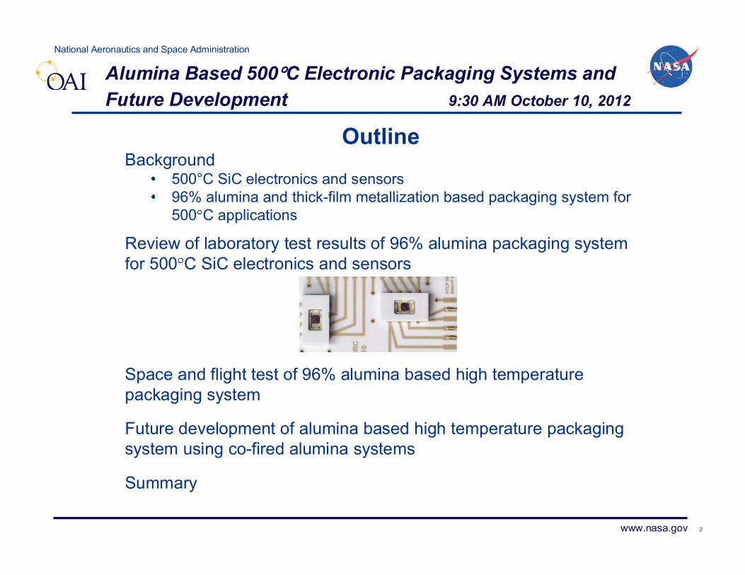
OutlineBackground
500°C SiC electronics and sensors96% alumina and thick-film metallization based packaging system for500 C applications
Review of laboratory test results of 96% alumina packaging systemfor 500 C SiC electronics and sensors
Space and flight test of 96% alumina based high temperaturepackaging system
Future development of alumina based high temperature packagingsystem using co-fired alumina systems
Summary
National Aeronautics and Space Administration
www.nasa.gov 3
Alumina Based 500 C Electronic Packaging Systems andFuture Development
Background
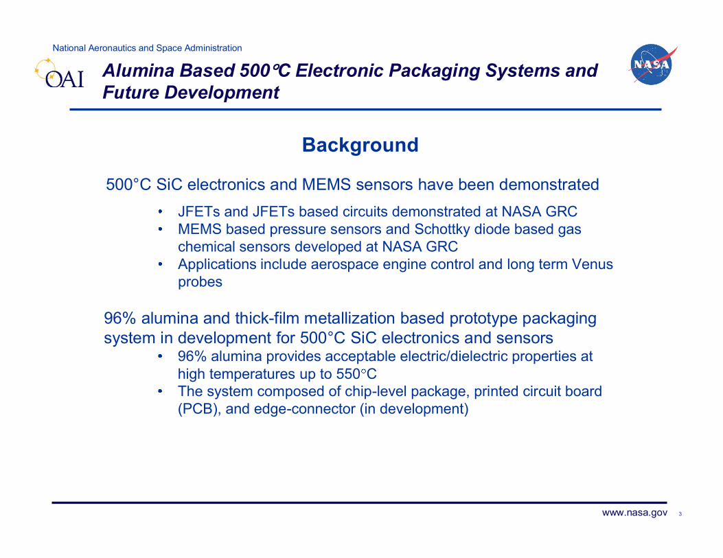
500°C SiC electronics and MEMS sensors have been demonstratedJFETs and JFETs based circuits demonstrated at NASA GRCMEMS based pressure sensors and Schottky diode based gaschemical sensors developed at NASA GRCApplications include aerospace engine control and long term Venusprobes
96% alumina and thick-film metallization based prototype packagingsystem in development for 500°C SiC electronics and sensors
96% alumina provides acceptable electric/dielectric properties athigh temperatures up to 550 CThe system composed of chip-level package, printed circuit board(PCB), and edge-connector (in development)
National Aeronautics and Space Administration
www.nasa.gov 4
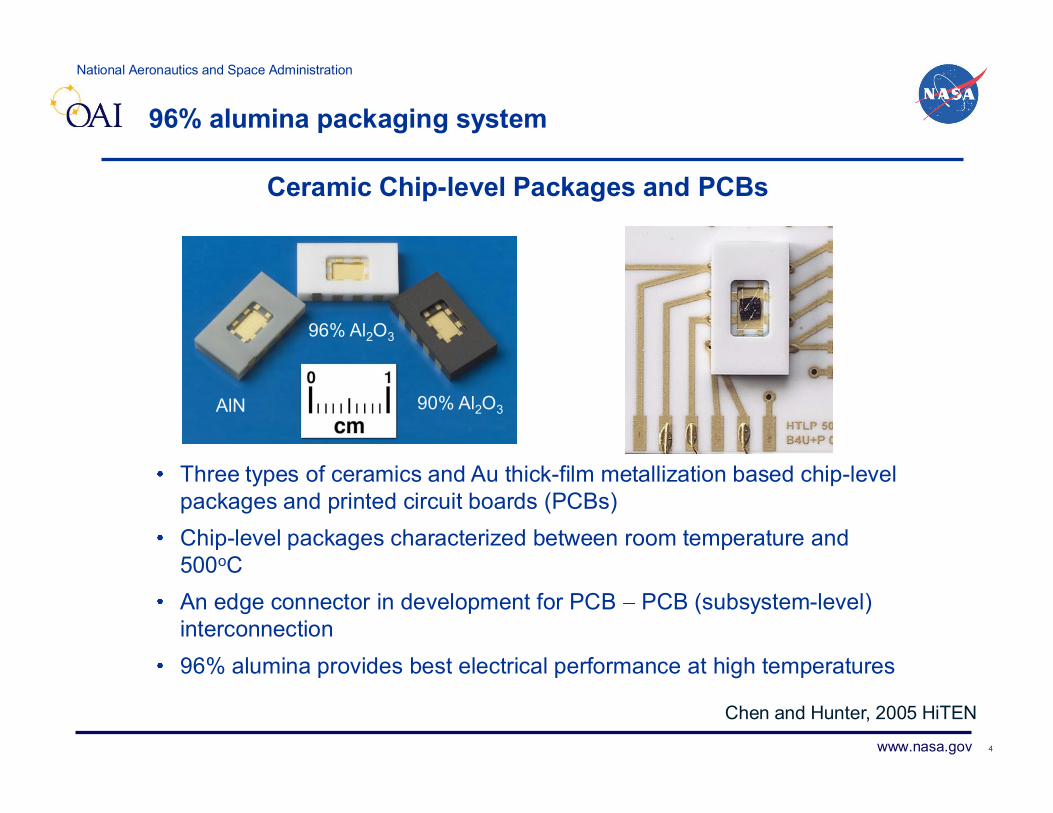
96% alumina packaging system
AlN
96% Al2O3
90% Al2O3
Three types of ceramics and Au thick-film metallization based chip-levelpackages and printed circuit boards (PCBs)Chip-level packages characterized between room temperature and500oCAn edge connector in development for PCB PCB (subsystem-level)interconnection96% alumina provides best electrical performance at high temperatures
Ceramic Chip-level Packages and PCBs
Chen and Hunter, 2005 HiTEN
National Aeronautics and Space Administration
www.nasa.gov 5
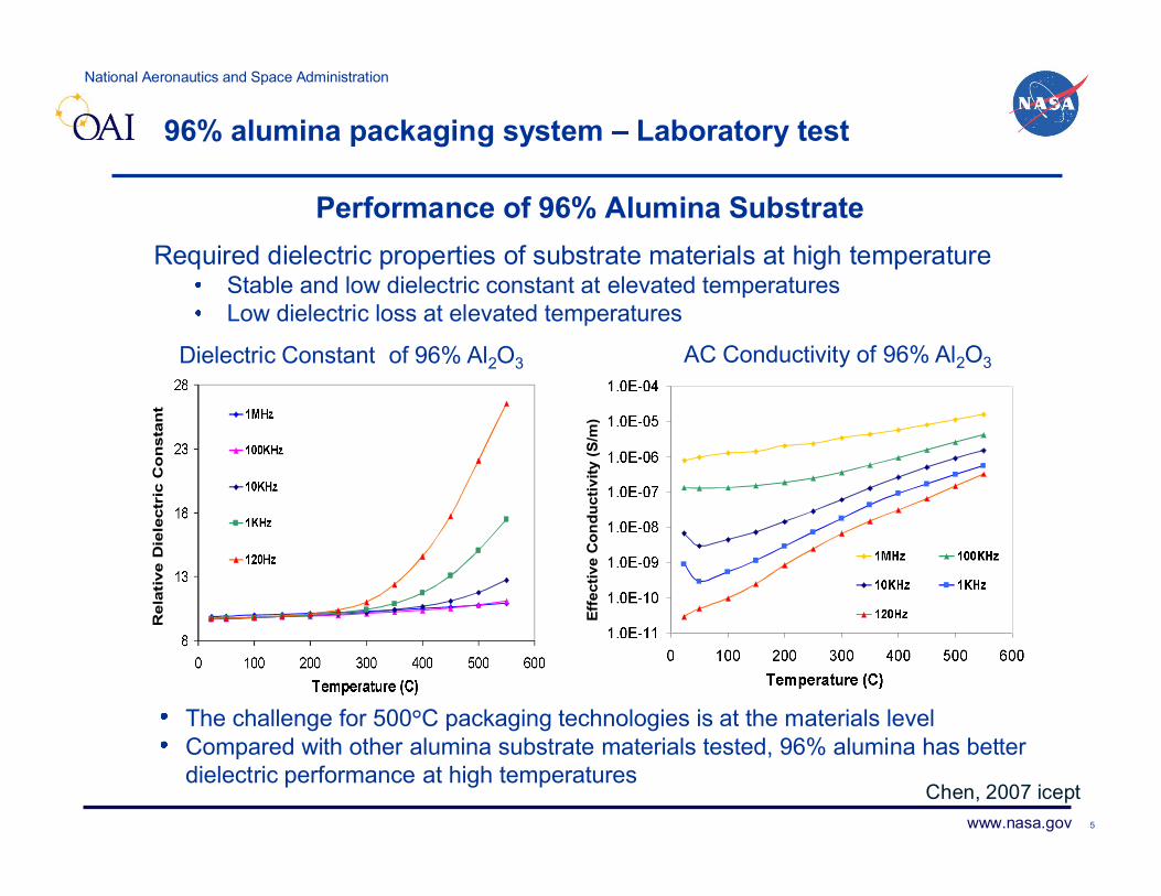
96% alumina packaging system Laboratory test
Performance of 96% Alumina SubstrateRequired dielectric properties of substrate materials at high temperature
Stable and low dielectric constant at elevated temperaturesLow dielectric loss at elevated temperatures
Rel
ativ
e D
iele
ctri
c C
on
stan
t
Effe
ctiv
e C
ondu
ctiv
ity (S
/m)
AC Conductivity of 96% Al2O3Dielectric Constant of 96% Al2O3
The challenge for 500°C packaging technologies is at the materials levelCompared with other alumina substrate materials tested, 96% alumina has betterdielectric performance at high temperatures
Chen, 2007 icept
National Aeronautics and Space Administration
www.nasa.gov 6
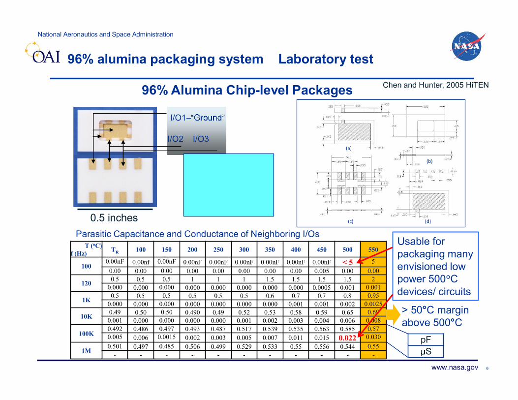
96% alumina packaging system Laboratory test
I/O1
I/O2 I/O3
Parasitic Capacitance and Conductance of Neighboring I/Os
Parasitic Equivalent
I/Oi
I/Oj
96% Alumina Chip-level Packages
T (oC)f (Hz) TR 100 150 200 250 300 350 400 450 500 550
1000.00nF 0.00nf 0.00nF 0.00nF 0.00nF 0.00nF 0.00nF 0.00nF 0.00nF < 5 5
0.00 0.00 0.00 0.00 0.00 0.00 0.00 0.00 0.005 0.00 0.00
120 0.5 0.5 0.5 1 1 1 1.5 1.5 1.5 1.5 20.000 0.000 0.000 0.000 0.000 0.000 0.000 0.000 0.0005 0.001 0.001
1K0.5 0.5 0.5 0.5 0.5 0.5 0.6 0.7 0.7 0.8 0.95
0.000 0.000 0.000 0.000 0.000 0.000 0.000 0.001 0.001 0.002 0.0025
10K0.49 0.50 0.50 0.490 0.49 0.52 0.53 0.58 0.59 0.65 0.690.001 0.000 0.000 0.000 0.000 0.001 0.002 0.003 0.004 0.006 0.008
100K0.492 0.486 0.497 0.493 0.487 0.517 0.539 0.535 0.563 0.585 0.570.005 0.006 0.0015 0.002 0.003 0.005 0.007 0.011 0.015 0.022 0.030
1M0.501 0.497 0.485 0.506 0.499 0.529 0.533 0.55 0.556 0.544 0.55
- - - - - - - - - - -
(b)
(c) (d)
(a)
0.5 inches
Usable forpackaging manyenvisioned lowpower 500°Cdevices/ circuits
> 50°C marginabove 500°C
pFS
Chen and Hunter, 2005 HiTEN
National Aeronautics and Space Administration
www.nasa.gov 7
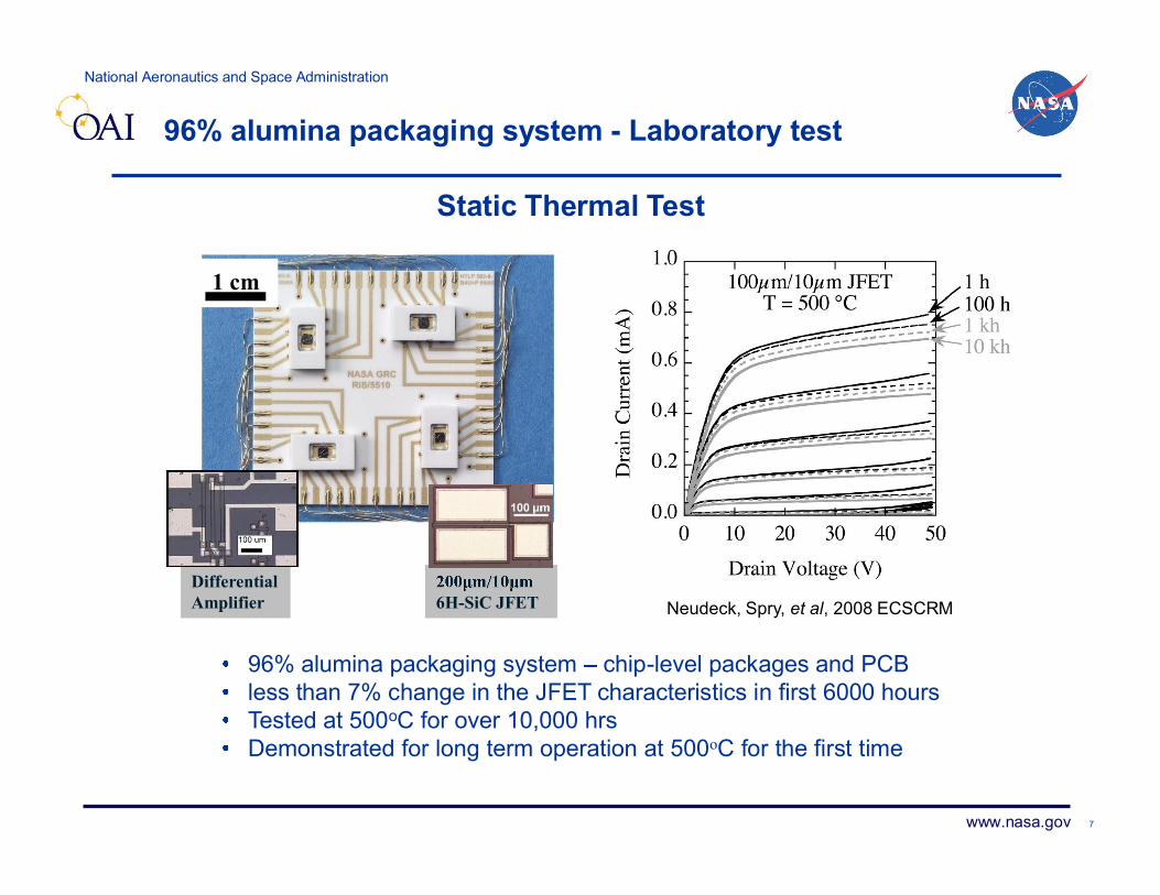
96% alumina packaging system - Laboratory test
Al2O3
Al2O3
Static Thermal Test
1 cm
6H-SiC JFETDifferentialAmplifier Neudeck, Spry, et al, 2008 ECSCRM
96% alumina packaging system chip-level packages and PCBless than 7% change in the JFET characteristics in first 6000 hoursTested at 500oC for over 10,000 hrsDemonstrated for long term operation at 500oC for the first time
National Aeronautics and Space Administration
www.nasa.gov
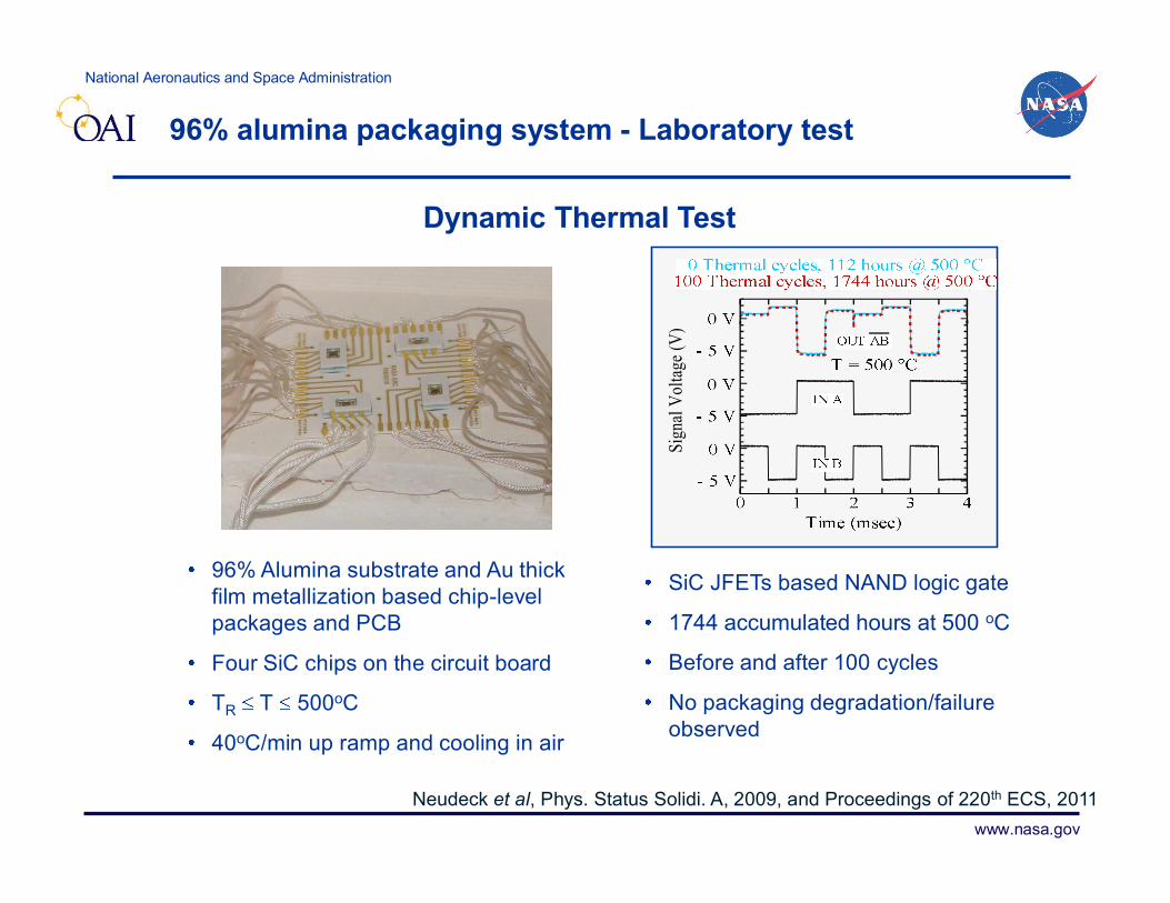
Dynamic Thermal Test
96% alumina packaging system - Laboratory test
96% Alumina substrate and Au thickfilm metallization based chip-levelpackages and PCB
Four SiC chips on the circuit board
TR T 500oC
40oC/min up ramp and cooling in air
Sign
al Vo
ltage
(V)
SiC JFETs based NAND logic gate
1744 accumulated hours at 500 oC
Before and after 100 cycles
No packaging degradation/failureobserved
Neudeck et al, Phys. Status Solidi. A, 2009, and Proceedings of 220th ECS, 2011
National Aeronautics and Space Administration
www.nasa.gov
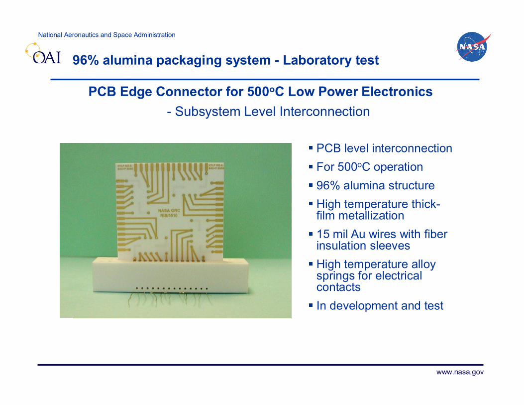
96% alumina packaging system - Laboratory test
PCB Edge Connector for 500oC Low Power Electronics- Subsystem Level Interconnection
PCB level interconnectionFor 500oC operation96% alumina structureHigh temperature thick-film metallization15 mil Au wires with fiberinsulation sleevesHigh temperature alloysprings for electricalcontactsIn development and test
National Aeronautics and Space Administration
www.nasa.gov 10
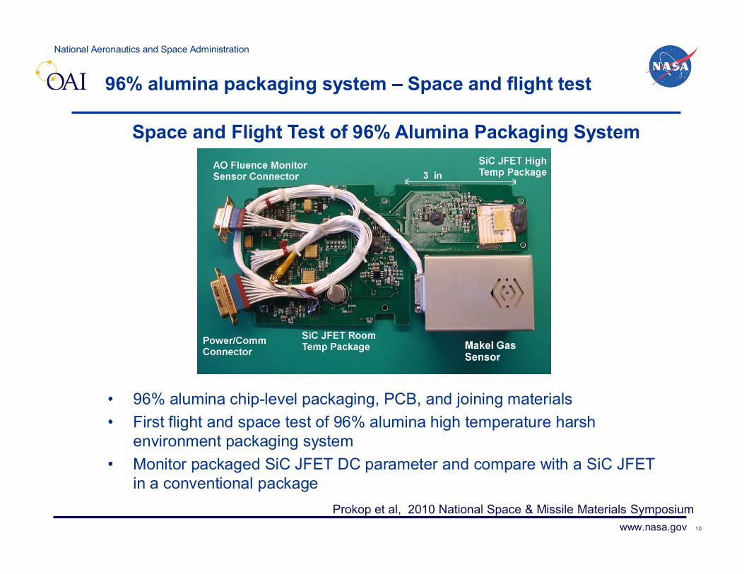
96% alumina packaging system Space and flight test
96% Al2O3
90% Al2O3
Space and Flight Test of 96% Alumina Packaging System
96% alumina chip-level packaging, PCB, and joining materialsFirst flight and space test of 96% alumina high temperature harshenvironment packaging systemMonitor packaged SiC JFET DC parameter and compare with a SiC JFETin a conventional package
Prokop et al, 2010 National Space & Missile Materials Symposium
National Aeronautics and Space Administration
www.nasa.gov 11
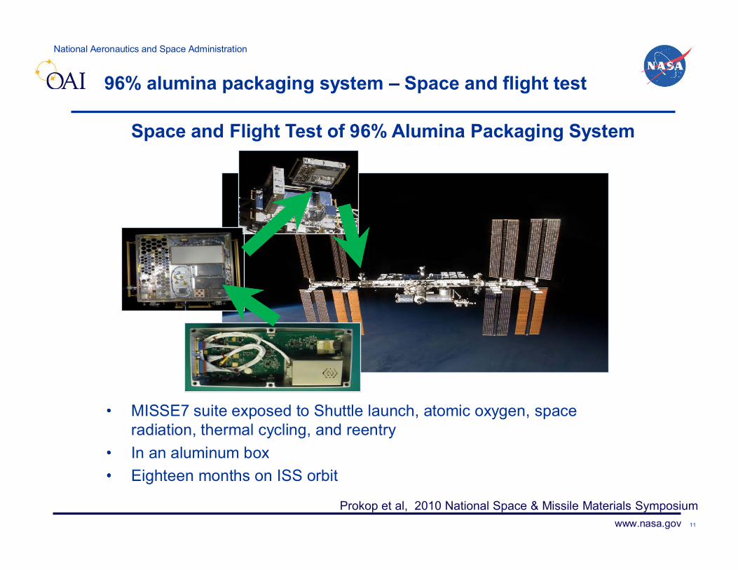
96% alumina packaging system Space and flight test
96% Al2O3
90% Al2O3
Space and Flight Test of 96% Alumina Packaging System
MISSE7 suite exposed to Shuttle launch, atomic oxygen, spaceradiation, thermal cycling, and reentryIn an aluminum boxEighteen months on ISS orbit
Prokop et al, 2010 National Space & Missile Materials Symposium
National Aeronautics and Space Administration
www.nasa.gov
96% alumina packaging system Space and flight test
12
Dra
in C
urrn
et I D
(mA
)
Dra
in C
urrn
et I D
(mA
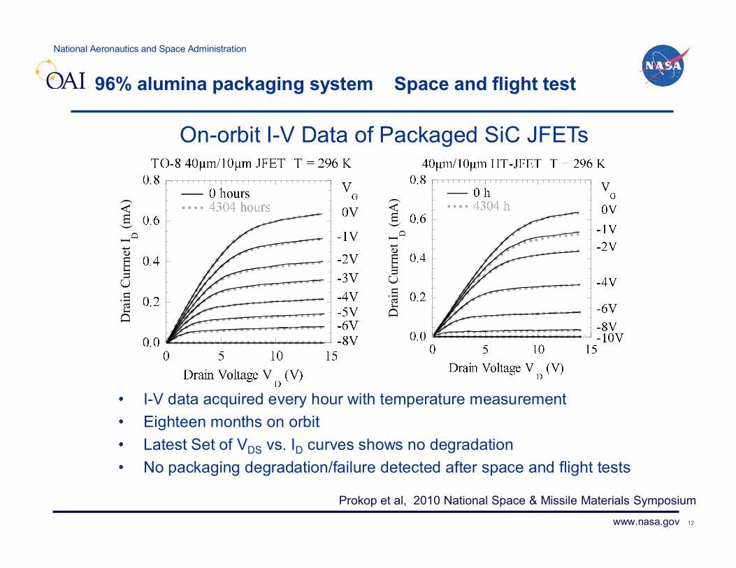
)I-V data acquired every hour with temperature measurementEighteen months on orbitLatest Set of VDS vs. ID curves shows no degradationNo packaging degradation/failure detected after space and flight tests
On-orbit I-V Data of Packaged SiC JFETs
Prokop et al, 2010 National Space & Missile Materials Symposium
National Aeronautics and Space Administration
www.nasa.gov
Future development of alumina high temperature packagingsystems
LTCC and HTCC Alumina96% alumina substrate based packaging system
Dielectric properties of 96% alumina measured at temperatures up to550 CExcellent electrical and dielectric properties as substrate for conventionalelectronicsThin-film and thick-film metallization available96% alumina packaging system long term tested with SiC electronics at500oCChip-level packages not fabricated with co-fired process
Low temperature and high temperature co-fired (LTCC and HTCC)alumina substrates ?
A few percent of glass used in co-fired alumina systemsSuitable for large scale commercializationDielectric performance at high temperatures?Metallization scheme?
National Aeronautics and Space Administration
www.nasa.gov
Future development of alumina high temperature packagingsystems
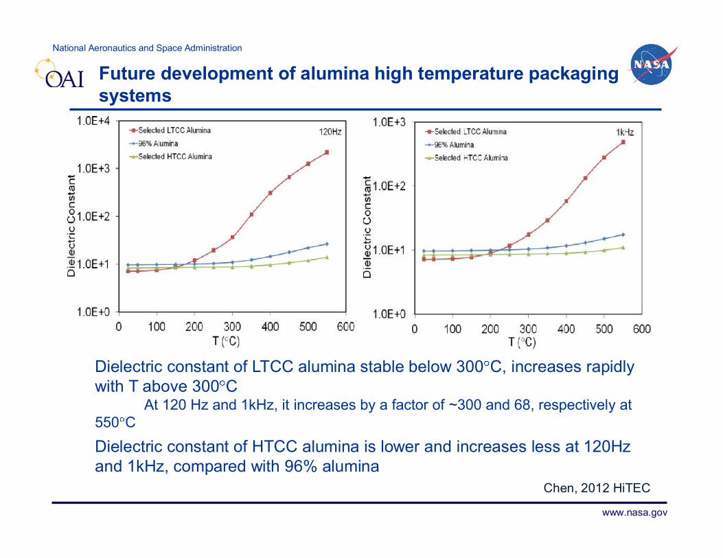
Dielectric constant of LTCC alumina stable below 300 C, increases rapidlywith T above 300 C
At 120 Hz and 1kHz, it increases by a factor of ~300 and 68, respectively at550 C
Dielectric constant of HTCC alumina is lower and increases less at 120Hzand 1kHz, compared with 96% alumina
Chen, 2012 HiTEC
National Aeronautics and Space Administration
www.nasa.gov
Future development of alumina high temperature packagingsystems
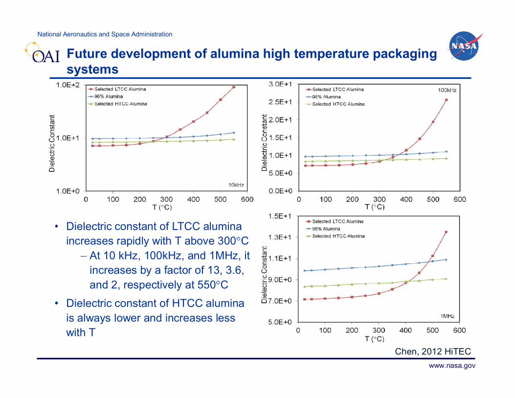
Dielectric constant of LTCC aluminaincreases rapidly with T above 300 C
At 10 kHz, 100kHz, and 1MHz, itincreases by a factor of 13, 3.6,and 2, respectively at 550 C
Dielectric constant of HTCC aluminais always lower and increases lesswith T
Chen, 2012 HiTEC
National Aeronautics and Space Administration
www.nasa.gov
Future development of alumina high temperature packagingsystems
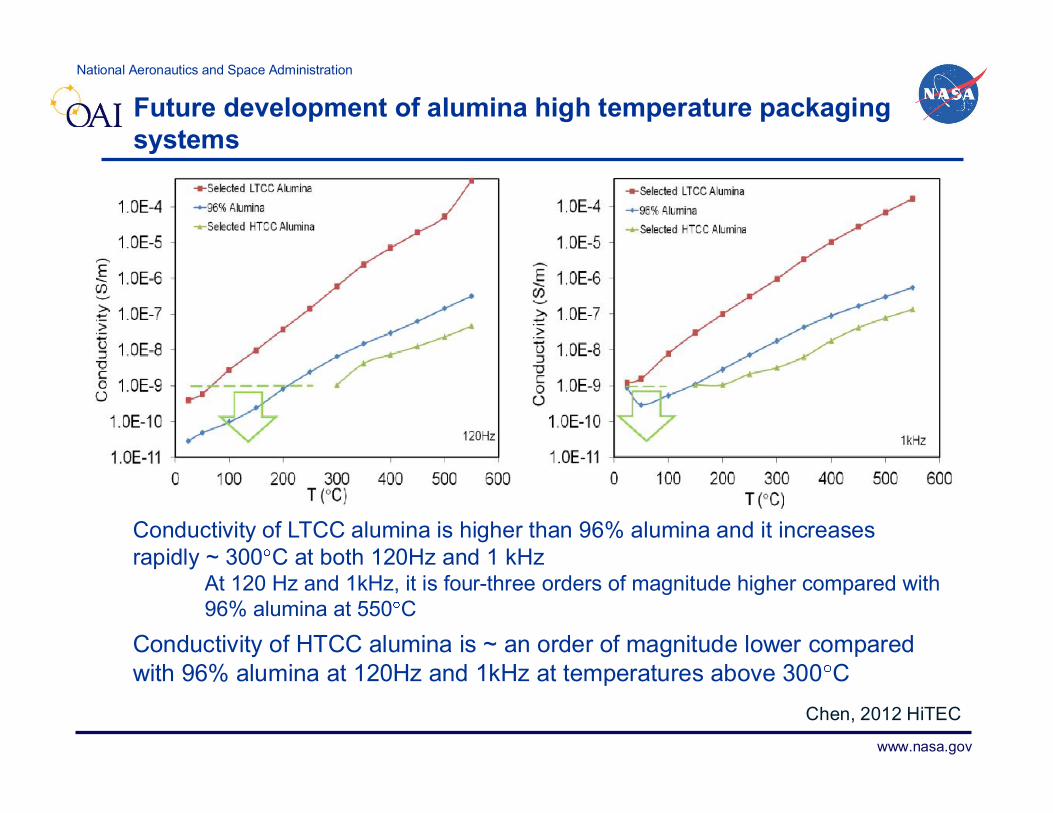
Conductivity of LTCC alumina is higher than 96% alumina and it increasesrapidly ~ 300 C at both 120Hz and 1 kHz
At 120 Hz and 1kHz, it is four-three orders of magnitude higher compared with96% alumina at 550 C
Conductivity of HTCC alumina is ~ an order of magnitude lower comparedwith 96% alumina at 120Hz and 1kHz at temperatures above 300 C
Chen, 2012 HiTEC
National Aeronautics and Space Administration
www.nasa.gov
Future development of alumina high temperature packagingsystems
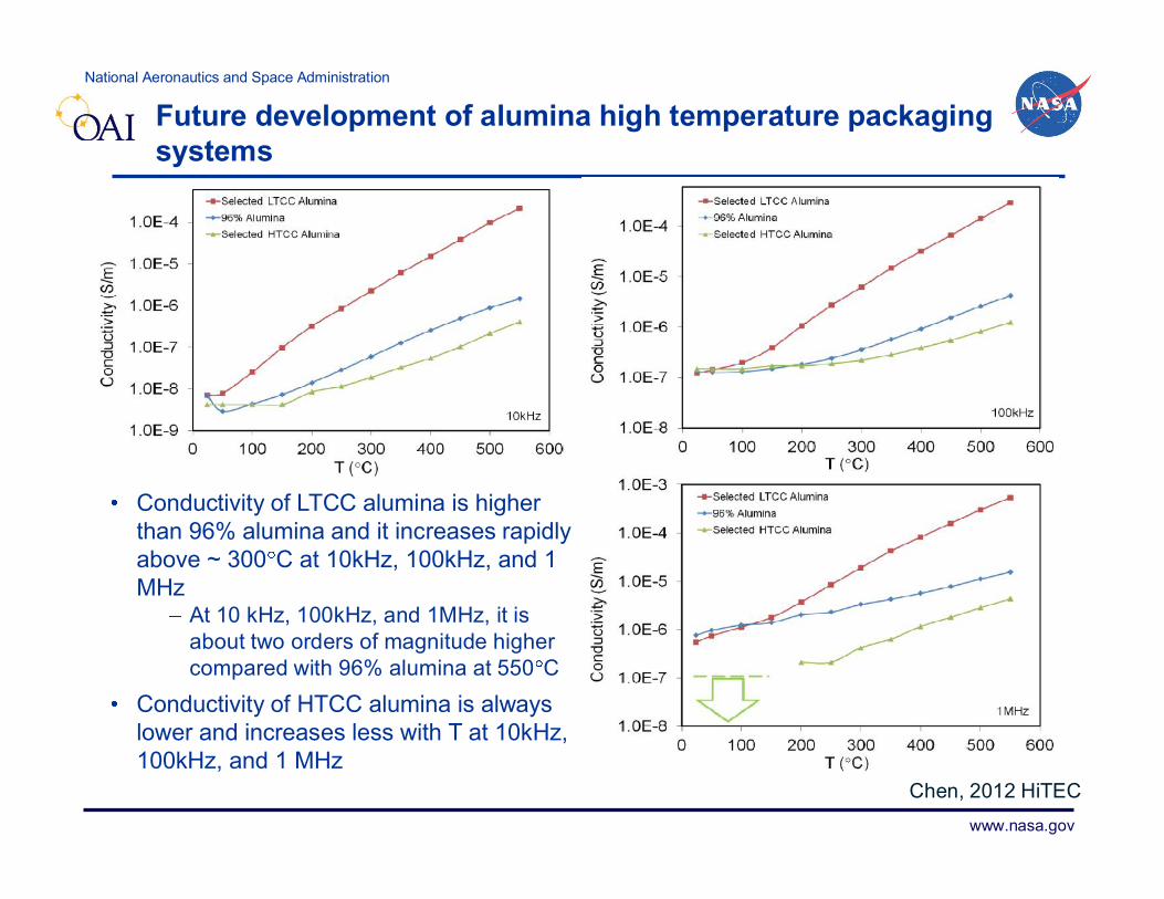
Conductivity of LTCC alumina is higherthan 96% alumina and it increases rapidlyabove ~ 300 C at 10kHz, 100kHz, and 1MHz
At 10 kHz, 100kHz, and 1MHz, it isabout two orders of magnitude highercompared with 96% alumina at 550 C
Conductivity of HTCC alumina is alwayslower and increases less with T at 10kHz,100kHz, and 1 MHz
Chen, 2012 HiTEC
National Aeronautics and Space Administration
www.nasa.gov
Future development of alumina high temperature packagingsystems
Compared with 96% alumina
Dielectric constant and AC conductivity of LTCC alumina increasewith T rapidly above 300 C, so this material is more suitable for thetemperature range below 350 C
Dielectric constant of HTCC alumina is slightly lower and it increasesless with temperature. AC conductivity of this material is also lowerthan that of 96% alumina at temperatures above 200 CDissipation factor of LTCC alumina is always higher at temperaturesabove 100 CDissipation factor of HTCC alumina is always lower compared withthat of 96% alumina at temperatures above 250 C
HTCC alumina is also better for hermetic sealing
Alumina based binders used for HTCC thick-film materials areexpected to be thermal dynamically stable in a wide temperaturerange
National Aeronautics and Space Administration
www.nasa.gov 19
Alumina Based 500 C Electronic Packaging Systems and FutureDevelopment 10:10 AM October 10, 2012
Summary96% alumina substrate and thick-film metallization based packagingsystems demonstrated at 500°C
Alumina and aluminum nitride chip-level packages and PCBsEdge-connector in development and testStatic thermal test of packaged SiC JFET circuits successfully over 10,000hours at 500°CThermal dynamic test between room temperature and 500 CTested in Shuttle flight, and ISS low earth orbit for eighteen monthsChip-level packages not fully commercially fabricated
HTCC alumina systemSelected material characterized and tested at temperatures up to 550°Lower parasitic effectsMore suitable for large scale commercializationAlumina binder for HTCC alumina systems are expected to be stable athigh temperaturesFurther development needed
National Aeronautics and Space Administration
www.nasa.gov 20
Thank You Very Much for Your Attention!
Acknowledgements
Author acknowledges contributions of Philip G. Neudeck, GaryW. Hunter, Norman F. Prokop, Lawrence C. Greer, Michael J.Krasowski, and Danny C. Spina at NASA Glenn Research Center.Author thanks Drs. Lawrence G. Matus, Mary V. Zeller, and Gary T.Seng for their support. The high temperature packaging researchis currently supported by Vehicle Systems Safety Technologies(VSST) project of NASA Aviation Safety program and DistributedEngine Control task of the Subsonic Fixed Wing project within theFundamental Aeronautics Program.