alternator control ic with lin interface
TRANSCRIPT
Data Sheet Rev. 1.00www.infineon.com 1 2019-05-29
TLE8881-2Alternator Control IC with LIN Interface
Features• Single-chip alternator control IC• High-side n-channel DMOS output stage with RDSON of 60 mΩ typ. (at 25°C)
/ 110 mΩ max.• Excitation PWM duty cycle range from 0% up to 100%• Full digital and fast PI regulator• EEPROM for customization to the target application• Compliant to both communication standard specifications LIN 2.1 (on
physical layer and data link layer) and LIN 1.3 (on data link layer) with baudrate up to 19200 bit/s - selectable via EEPROM
• Compatible to several OEM specification variants• Digital temperature setpoint compensation• Excitation current limitation depending on LIN commands • Extensive voltage measurement range of 8 V up to 24 V• Very low stand-by current of less than 80 μA @ 25°C• High ESD resistivity of 8 kV on all lines (ESD HBM)• High temperature range of -40°C up to 175°C• Green product (RoHS-compliant)
Potential applications• Voltage regulator for externally excited alternator/generator machine
Product validationQualified for automotive applications. Product validation according to AEC-Q100.
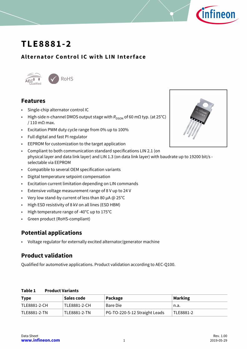
Table 1 Product VariantsType Sales code Package MarkingTLE8881-2-CH TLE8881-2-CH Bare Die n.a.
TLE8881-2-TN TLE8881-2-TN PG-TO-220-5-12 Straight Leads TLE8881-2
Data Sheet 2 Rev. 1.00 2019-05-29
TLE8881-2Alternator Control IC with LIN Interface
DescriptionThe device is based on Infineon’s power technology SPT which allows bipolar and CMOS control circuitry tobe integrated with DMOS power devices on the same monolithic circuitry.The battery voltage is regulated at a precise value between 10.6 V and 16 V. In case of communication loss, theregulator is able to proceed with the voltage regulation by using adjustable default values. A fixed frequencyPWM voltage is set at an output pin to excite the excitation coil of the alternator.The TLE8881-2 is equipped with special protection circuitry as well as circuitry to control the excitationvoltage slew rate to reduce EMI. Therefore the device meets the specific ESD and EMC requirement of the harshautomotive environment.The following main features are implemented:
Closed loop voltage controlBy controlling the excitation PWM duty cycle of the excitation output stage, the TLE8881-2 regulates theoutput voltage to an internal default voltage setpoint or to a voltage setpoint controlled by the enginemanagement or energy management ECU via the LIN interface. The regulation is processed in a full digital andfast PI regulator.
Load Response Control (LRC)The load response control (LRC) prevents engine speed hunting and vibration due to electrical loads whichcause abrupt torque loading of the engine at low speeds.
Self start detectionThe TLE8881-2 automatically wakes up the state machine if the frequency and amplitude of the phase signalis above a specific threshold. This allows the alternator to function in spite of interrupted or broken LINcommunication.
Pre-excitationThe excitation coil is pre-energized with a small fixed excitation PWM duty cycle coming from the excitationoutput stage of the TLE8881-2 to provide a stable phase voltage input signal.
Phase Signal Boost (PSB)The phase signal boost system of the TLE8881-2 maintains a proper phase signal for rotor speedmeasurement.
Low Voltage Excitation Switch On (LEO)At very low battery voltage loading is immediately induced by increasing the current in the excitation coil untila minimal defined voltage is achieved.
High Voltage Excitation Switch Off (HEO)At very high boardnet voltage, the excitation is immediately switched off in order to stop generating power.
Excitation current measurementThe measurement of the excitation current inside the rotor is used by the ECU to calculate and monitor thetorque on the engine.
Data Sheet 3 Rev. 1.00 2019-05-29
TLE8881-2Alternator Control IC with LIN Interface
Excitation current limitationThe current limitation is used to set a boundary on the excitation current (meaning on the torque) via the LINinterface.
Frequency-dependent Excitation Current Limitation (FEXLIM)The current limitation is used to set a boundary on the current (meaning on the torque) and is dependent onrotation speed.
Temperature measurementThe TLE8881-2 is able to send its own measured junction temperature to the ECU via the LIN interface.
Temperature setpoint compensationThe voltage setpoint is gradually compensated depending on the measured temperature.
Voltage measurementThe TLE8881-2 is able to send the measured voltage at VBA input via the LIN interface.
Speed measurementThe TLE8881-2 is able to send the measured rotor speed to the ECU via the LIN interface.
Speed-dependent Ki-Kp parameter sets (KiKp)TLE8881-2 allows to use different regulation KiKp parameter sets for the regulation of the EXC duty cycledependent on the rotation speed nR of the alternator. The device provides 4 different but fixed KiKp parametersets which can be selected.
F-para switchingThe PI controller’s parameter sets can be adjusted during operation. This function offers the possibility toadjust the parameters depending on the pre-programmed parameter set and the activation via a LIN frame.
Voltage-dependent KiKp function (VoKiKp function)In order to avoid a slow reaction of the IC on relatively high VBA voltages compared to VSET, especially if slowKiKp parameter sets are chosen, the TLE8881-2 offers a voltage dependent KiKp function (VoKiKp).
Speed-dependent Lowering of the HEO limit (LowHEO function)In order to optimize the reaction to high VBA voltages in case of a low rotation speed, the TLE8881-2 offers afunction to lower the HEO limit in order to assure a fast reaction to high VBA voltages.
LIN interfaceIn addition to the classical functions of voltage regulation, this regulator offers a bi-directional serial datainterface which is fully compliant to the standard specification LIN 2.1 (on the physical layer and the data linklayer) and LIN 1.3 (on the data link layer) for communication with the engine management or energymanagement ECU. A dedicated EEPROM switch provides the possibility to change between LIN 1.3 or LIN 2.1on the data link layer.This communication link offers the following functions:• Control of the voltage setpoint as regulation input• Control of the LRC parameters

Data Sheet 4 Rev. 1.00 2019-05-29
TLE8881-2Alternator Control IC with LIN Interface
• Control of the excitation current limitation• Control of what regulation loop parameter set is used for optimized behavior with and without battery• Control of the temperature voltage compensation offset• Different frame configurations for VDA-A, VDA-B, OEM1, OEM2• Transmission of the excitation PWM duty cycle value at excitation output stage to ECU• Transmission of the excitation current value (determined by excitation current measurement) to ECU• Transmission of the voltage at VBA (determined by voltage measurement) to ECU• Transmission of the chip junction temperature to ECU• Transmission of the rotation speed (using speed measurement) to ECU• Transmission of the alternator’s system supplier code to ECU• Transmission of the alternator’s class code to ECU• Transmission of the regulator identification code to ECU• Transmission of diagnosis (defects detection) to ECU: high temperature (F-HT), rotor failure (F-ROT),
electrical failure (F-EL, debounced)• Transmission of the LIN diagnosis: communication error failure (F-CEF), communication time-out (F-CTO)

Data Sheet 5 Rev. 1.00 2019-05-29
TLE8881-2Alternator Control IC with LIN Interface
1 Block diagram . . . . . . . . . . . . . . . . . . . . . . . . . . . . . . . . . . . . . . . . . . . . . . . . . . . . . . . . . . . . . . . . . . . 8
2 Pin and pad configuration . . . . . . . . . . . . . . . . . . . . . . . . . . . . . . . . . . . . . . . . . . . . . . . . . . . . . . . . 102.1 Pin assignment for PG-TO-220-5-12 package . . . . . . . . . . . . . . . . . . . . . . . . . . . . . . . . . . . . . . . . . . . . . . . 10
3 General product characteristics . . . . . . . . . . . . . . . . . . . . . . . . . . . . . . . . . . . . . . . . . . . . . . . . . . . 113.1 Absolute maximum ratings . . . . . . . . . . . . . . . . . . . . . . . . . . . . . . . . . . . . . . . . . . . . . . . . . . . . . . . . . . . . . . . 113.2 Functional range . . . . . . . . . . . . . . . . . . . . . . . . . . . . . . . . . . . . . . . . . . . . . . . . . . . . . . . . . . . . . . . . . . . . . . . . 123.3 Thermal resistance . . . . . . . . . . . . . . . . . . . . . . . . . . . . . . . . . . . . . . . . . . . . . . . . . . . . . . . . . . . . . . . . . . . . . . 133.4 Reduced operating range . . . . . . . . . . . . . . . . . . . . . . . . . . . . . . . . . . . . . . . . . . . . . . . . . . . . . . . . . . . . . . . . . 13
4 Main control block . . . . . . . . . . . . . . . . . . . . . . . . . . . . . . . . . . . . . . . . . . . . . . . . . . . . . . . . . . . . . . . 144.1 State diagram . . . . . . . . . . . . . . . . . . . . . . . . . . . . . . . . . . . . . . . . . . . . . . . . . . . . . . . . . . . . . . . . . . . . . . . . . . . 144.2 Rotational speed events . . . . . . . . . . . . . . . . . . . . . . . . . . . . . . . . . . . . . . . . . . . . . . . . . . . . . . . . . . . . . . . . . . 154.3 LIN communication events . . . . . . . . . . . . . . . . . . . . . . . . . . . . . . . . . . . . . . . . . . . . . . . . . . . . . . . . . . . . . . . 164.4 State description . . . . . . . . . . . . . . . . . . . . . . . . . . . . . . . . . . . . . . . . . . . . . . . . . . . . . . . . . . . . . . . . . . . . . . . . 164.4.1 Feature priorities . . . . . . . . . . . . . . . . . . . . . . . . . . . . . . . . . . . . . . . . . . . . . . . . . . . . . . . . . . . . . . . . . . . . . . 164.4.2 “Stand-by” . . . . . . . . . . . . . . . . . . . . . . . . . . . . . . . . . . . . . . . . . . . . . . . . . . . . . . . . . . . . . . . . . . . . . . . . . . . . 174.4.3 State “ComActive” . . . . . . . . . . . . . . . . . . . . . . . . . . . . . . . . . . . . . . . . . . . . . . . . . . . . . . . . . . . . . . . . . . . . . 184.4.4 State “pre-excitation” . . . . . . . . . . . . . . . . . . . . . . . . . . . . . . . . . . . . . . . . . . . . . . . . . . . . . . . . . . . . . . . . . . 194.4.5 State “normal operation” . . . . . . . . . . . . . . . . . . . . . . . . . . . . . . . . . . . . . . . . . . . . . . . . . . . . . . . . . . . . . . 194.4.6 State “excitation off” . . . . . . . . . . . . . . . . . . . . . . . . . . . . . . . . . . . . . . . . . . . . . . . . . . . . . . . . . . . . . . . . . . . 204.4.7 State “default operation“ . . . . . . . . . . . . . . . . . . . . . . . . . . . . . . . . . . . . . . . . . . . . . . . . . . . . . . . . . . . . . . . 214.4.8 State “overtemperature” . . . . . . . . . . . . . . . . . . . . . . . . . . . . . . . . . . . . . . . . . . . . . . . . . . . . . . . . . . . . . . . 214.5 Diagnostic flags . . . . . . . . . . . . . . . . . . . . . . . . . . . . . . . . . . . . . . . . . . . . . . . . . . . . . . . . . . . . . . . . . . . . . . . . . 224.5.1 High-temperature diagnostic flag . . . . . . . . . . . . . . . . . . . . . . . . . . . . . . . . . . . . . . . . . . . . . . . . . . . . . . . . 234.5.2 Mechanical error flag . . . . . . . . . . . . . . . . . . . . . . . . . . . . . . . . . . . . . . . . . . . . . . . . . . . . . . . . . . . . . . . . . . . 234.5.3 Electrical error flag . . . . . . . . . . . . . . . . . . . . . . . . . . . . . . . . . . . . . . . . . . . . . . . . . . . . . . . . . . . . . . . . . . . . . 23
5 Regulation functions . . . . . . . . . . . . . . . . . . . . . . . . . . . . . . . . . . . . . . . . . . . . . . . . . . . . . . . . . . . . . 265.1 Control system . . . . . . . . . . . . . . . . . . . . . . . . . . . . . . . . . . . . . . . . . . . . . . . . . . . . . . . . . . . . . . . . . . . . . . . . . . 265.2 Excitation output driver . . . . . . . . . . . . . . . . . . . . . . . . . . . . . . . . . . . . . . . . . . . . . . . . . . . . . . . . . . . . . . . . . . 275.3 Excitation current measurement . . . . . . . . . . . . . . . . . . . . . . . . . . . . . . . . . . . . . . . . . . . . . . . . . . . . . . . . . . 285.4 Limitation of Excitation Current (CLIM) . . . . . . . . . . . . . . . . . . . . . . . . . . . . . . . . . . . . . . . . . . . . . . . . . . . . 295.5 Temperature measurement . . . . . . . . . . . . . . . . . . . . . . . . . . . . . . . . . . . . . . . . . . . . . . . . . . . . . . . . . . . . . . 295.6 Temperature Setpoint Compensation (TSC) . . . . . . . . . . . . . . . . . . . . . . . . . . . . . . . . . . . . . . . . . . . . . . . . 305.7 Voltage measurement . . . . . . . . . . . . . . . . . . . . . . . . . . . . . . . . . . . . . . . . . . . . . . . . . . . . . . . . . . . . . . . . . . . . 315.8 Speed measurement . . . . . . . . . . . . . . . . . . . . . . . . . . . . . . . . . . . . . . . . . . . . . . . . . . . . . . . . . . . . . . . . . . . . . 325.9 Low Voltage Excitation On (LEO) . . . . . . . . . . . . . . . . . . . . . . . . . . . . . . . . . . . . . . . . . . . . . . . . . . . . . . . . . . 325.10 High Voltage Excitation Off (HEO) . . . . . . . . . . . . . . . . . . . . . . . . . . . . . . . . . . . . . . . . . . . . . . . . . . . . . . . . . 345.11 Phase Signal Boost (PSB) . . . . . . . . . . . . . . . . . . . . . . . . . . . . . . . . . . . . . . . . . . . . . . . . . . . . . . . . . . . . . . . . . 365.12 Load Response Control (LRC) . . . . . . . . . . . . . . . . . . . . . . . . . . . . . . . . . . . . . . . . . . . . . . . . . . . . . . . . . . . . . 365.13 Frequency-dependent Excitation Current Limitation (FEXLIM) . . . . . . . . . . . . . . . . . . . . . . . . . . . . . . . 385.13.1 Parameters and limitation areas . . . . . . . . . . . . . . . . . . . . . . . . . . . . . . . . . . . . . . . . . . . . . . . . . . . . . . . . 395.13.2 Function activation/deactivation . . . . . . . . . . . . . . . . . . . . . . . . . . . . . . . . . . . . . . . . . . . . . . . . . . . . . . . . 395.13.3 FEXLIM vs. RCLIM register value . . . . . . . . . . . . . . . . . . . . . . . . . . . . . . . . . . . . . . . . . . . . . . . . . . . . . . . . . 395.13.4 Transition behaviors . . . . . . . . . . . . . . . . . . . . . . . . . . . . . . . . . . . . . . . . . . . . . . . . . . . . . . . . . . . . . . . . . . . 405.13.5 Function characteristics . . . . . . . . . . . . . . . . . . . . . . . . . . . . . . . . . . . . . . . . . . . . . . . . . . . . . . . . . . . . . . . . 405.13.6 Behavior with restore state function . . . . . . . . . . . . . . . . . . . . . . . . . . . . . . . . . . . . . . . . . . . . . . . . . . . . . 41
Table of Contents

Data Sheet 6 Rev. 1.00 2019-05-29
TLE8881-2Alternator Control IC with LIN Interface
5.14 Regulation parameters control via LIN (F-Para function) . . . . . . . . . . . . . . . . . . . . . . . . . . . . . . . . . . . . . 425.15 Speed-dependent KiKp parameter sets (KiKp function) . . . . . . . . . . . . . . . . . . . . . . . . . . . . . . . . . . . . . . 425.16 Voltage-dependent KiKp function (VoKiKp function) . . . . . . . . . . . . . . . . . . . . . . . . . . . . . . . . . . . . . . . . 445.17 Speed-dependent lowering of the HEO limit (LowHEO function) . . . . . . . . . . . . . . . . . . . . . . . . . . . . . . 46
6 LIN interface . . . . . . . . . . . . . . . . . . . . . . . . . . . . . . . . . . . . . . . . . . . . . . . . . . . . . . . . . . . . . . . . . . . . 476.1 Bus topology . . . . . . . . . . . . . . . . . . . . . . . . . . . . . . . . . . . . . . . . . . . . . . . . . . . . . . . . . . . . . . . . . . . . . . . . . . . . 476.2 Signal specification (physical layer) . . . . . . . . . . . . . . . . . . . . . . . . . . . . . . . . . . . . . . . . . . . . . . . . . . . . . . . 486.3 Message frames (data link layer) . . . . . . . . . . . . . . . . . . . . . . . . . . . . . . . . . . . . . . . . . . . . . . . . . . . . . . . . . . 516.3.1 LIN frame structure . . . . . . . . . . . . . . . . . . . . . . . . . . . . . . . . . . . . . . . . . . . . . . . . . . . . . . . . . . . . . . . . . . . . 526.3.2 LIN frame identifier recommendations . . . . . . . . . . . . . . . . . . . . . . . . . . . . . . . . . . . . . . . . . . . . . . . . . . . 536.3.3 LIN RX frame . . . . . . . . . . . . . . . . . . . . . . . . . . . . . . . . . . . . . . . . . . . . . . . . . . . . . . . . . . . . . . . . . . . . . . . . . . 556.3.4 LIN TX1 frame . . . . . . . . . . . . . . . . . . . . . . . . . . . . . . . . . . . . . . . . . . . . . . . . . . . . . . . . . . . . . . . . . . . . . . . . . 566.3.5 LIN TX2 frame . . . . . . . . . . . . . . . . . . . . . . . . . . . . . . . . . . . . . . . . . . . . . . . . . . . . . . . . . . . . . . . . . . . . . . . . . 566.3.6 LIN TX3 frame . . . . . . . . . . . . . . . . . . . . . . . . . . . . . . . . . . . . . . . . . . . . . . . . . . . . . . . . . . . . . . . . . . . . . . . . . 576.4 LIN registers . . . . . . . . . . . . . . . . . . . . . . . . . . . . . . . . . . . . . . . . . . . . . . . . . . . . . . . . . . . . . . . . . . . . . . . . . . . . 586.4.1 Register RVSET (voltage setpoint) . . . . . . . . . . . . . . . . . . . . . . . . . . . . . . . . . . . . . . . . . . . . . . . . . . . . . . . 586.4.2 RVSET reporting via LIN . . . . . . . . . . . . . . . . . . . . . . . . . . . . . . . . . . . . . . . . . . . . . . . . . . . . . . . . . . . . . . . . . 596.4.3 Registers LRC (load response control) . . . . . . . . . . . . . . . . . . . . . . . . . . . . . . . . . . . . . . . . . . . . . . . . . . . . 596.4.4 Register RCLIM (excitation current limitation) . . . . . . . . . . . . . . . . . . . . . . . . . . . . . . . . . . . . . . . . . . . . . 626.4.5 Register RFPARA (F-Para function) . . . . . . . . . . . . . . . . . . . . . . . . . . . . . . . . . . . . . . . . . . . . . . . . . . . . . . . 646.4.6 Register RHT (adjustment of high temperature threshold) . . . . . . . . . . . . . . . . . . . . . . . . . . . . . . . . . 656.4.7 Register RDI (response data indicator) . . . . . . . . . . . . . . . . . . . . . . . . . . . . . . . . . . . . . . . . . . . . . . . . . . . 656.4.8 Register RDC (excitation PWM duty cycle) . . . . . . . . . . . . . . . . . . . . . . . . . . . . . . . . . . . . . . . . . . . . . . . . 666.4.9 Register RMC (measured excitation current) . . . . . . . . . . . . . . . . . . . . . . . . . . . . . . . . . . . . . . . . . . . . . . 666.4.10 Register RMT (measured temperature on chip) . . . . . . . . . . . . . . . . . . . . . . . . . . . . . . . . . . . . . . . . . . . . 666.4.11 Register RMV (measured voltage at VBA terminal) . . . . . . . . . . . . . . . . . . . . . . . . . . . . . . . . . . . . . . . . . 676.4.12 Register RMS (measured speed) . . . . . . . . . . . . . . . . . . . . . . . . . . . . . . . . . . . . . . . . . . . . . . . . . . . . . . . . . 686.4.13 Register RSUPP and RCLASS . . . . . . . . . . . . . . . . . . . . . . . . . . . . . . . . . . . . . . . . . . . . . . . . . . . . . . . . . . . . 756.5 Default register content . . . . . . . . . . . . . . . . . . . . . . . . . . . . . . . . . . . . . . . . . . . . . . . . . . . . . . . . . . . . . . . . . . 756.6 Register output filters . . . . . . . . . . . . . . . . . . . . . . . . . . . . . . . . . . . . . . . . . . . . . . . . . . . . . . . . . . . . . . . . . . . . 776.6.1 Filter for excitation PWM duty cycle (RDC filter) . . . . . . . . . . . . . . . . . . . . . . . . . . . . . . . . . . . . . . . . . . . 776.6.2 Filter for voltage measurement (RMV Filter) . . . . . . . . . . . . . . . . . . . . . . . . . . . . . . . . . . . . . . . . . . . . . . 786.6.3 Excitation current filter (RMC filter) . . . . . . . . . . . . . . . . . . . . . . . . . . . . . . . . . . . . . . . . . . . . . . . . . . . . . . 796.7 LIN 2.1 diagnostic frames . . . . . . . . . . . . . . . . . . . . . . . . . . . . . . . . . . . . . . . . . . . . . . . . . . . . . . . . . . . . . . . . . 806.7.1 Node configuration / identification . . . . . . . . . . . . . . . . . . . . . . . . . . . . . . . . . . . . . . . . . . . . . . . . . . . . . . 806.7.2 NAD, supplier ID, function ID and variant . . . . . . . . . . . . . . . . . . . . . . . . . . . . . . . . . . . . . . . . . . . . . . . . . 806.7.3 Assign frame ID range (LIN 2.1 service) . . . . . . . . . . . . . . . . . . . . . . . . . . . . . . . . . . . . . . . . . . . . . . . . . . . 816.7.4 Read by identifier (LIN 2.1 service) . . . . . . . . . . . . . . . . . . . . . . . . . . . . . . . . . . . . . . . . . . . . . . . . . . . . . . . 826.8 Programming Mode . . . . . . . . . . . . . . . . . . . . . . . . . . . . . . . . . . . . . . . . . . . . . . . . . . . . . . . . . . . . . . . . . . . . . . 826.9 Internal LIN timers . . . . . . . . . . . . . . . . . . . . . . . . . . . . . . . . . . . . . . . . . . . . . . . . . . . . . . . . . . . . . . . . . . . . . . . 83
7 Phase monitoring block . . . . . . . . . . . . . . . . . . . . . . . . . . . . . . . . . . . . . . . . . . . . . . . . . . . . . . . . . . 847.1 Block diagram . . . . . . . . . . . . . . . . . . . . . . . . . . . . . . . . . . . . . . . . . . . . . . . . . . . . . . . . . . . . . . . . . . . . . . . . . . . 847.2 Self-start wake-up . . . . . . . . . . . . . . . . . . . . . . . . . . . . . . . . . . . . . . . . . . . . . . . . . . . . . . . . . . . . . . . . . . . . . . . 847.3 Speed detection . . . . . . . . . . . . . . . . . . . . . . . . . . . . . . . . . . . . . . . . . . . . . . . . . . . . . . . . . . . . . . . . . . . . . . . . . 857.4 Phase monitoring . . . . . . . . . . . . . . . . . . . . . . . . . . . . . . . . . . . . . . . . . . . . . . . . . . . . . . . . . . . . . . . . . . . . . . . . 85
8 Core functions . . . . . . . . . . . . . . . . . . . . . . . . . . . . . . . . . . . . . . . . . . . . . . . . . . . . . . . . . . . . . . . . . . 86

Data Sheet 7 Rev. 1.00 2019-05-29
TLE8881-2Alternator Control IC with LIN Interface
8.1 Voltage reference . . . . . . . . . . . . . . . . . . . . . . . . . . . . . . . . . . . . . . . . . . . . . . . . . . . . . . . . . . . . . . . . . . . . . . . . 868.2 Internal supply reference . . . . . . . . . . . . . . . . . . . . . . . . . . . . . . . . . . . . . . . . . . . . . . . . . . . . . . . . . . . . . . . . . 868.3 Oscillator . . . . . . . . . . . . . . . . . . . . . . . . . . . . . . . . . . . . . . . . . . . . . . . . . . . . . . . . . . . . . . . . . . . . . . . . . . . . . . . 868.4 Charge pump . . . . . . . . . . . . . . . . . . . . . . . . . . . . . . . . . . . . . . . . . . . . . . . . . . . . . . . . . . . . . . . . . . . . . . . . . . . . 868.5 Restore state function . . . . . . . . . . . . . . . . . . . . . . . . . . . . . . . . . . . . . . . . . . . . . . . . . . . . . . . . . . . . . . . . . . . . 878.5.1 Supply micro-cut . . . . . . . . . . . . . . . . . . . . . . . . . . . . . . . . . . . . . . . . . . . . . . . . . . . . . . . . . . . . . . . . . . . . . . 878.5.2 Restore state event . . . . . . . . . . . . . . . . . . . . . . . . . . . . . . . . . . . . . . . . . . . . . . . . . . . . . . . . . . . . . . . . . . . . 88
9 Non-Volatile Memory (NVM) . . . . . . . . . . . . . . . . . . . . . . . . . . . . . . . . . . . . . . . . . . . . . . . . . . . . . . . 899.1 NVM characteristics . . . . . . . . . . . . . . . . . . . . . . . . . . . . . . . . . . . . . . . . . . . . . . . . . . . . . . . . . . . . . . . . . . . . . . 899.2 NVM register description . . . . . . . . . . . . . . . . . . . . . . . . . . . . . . . . . . . . . . . . . . . . . . . . . . . . . . . . . . . . . . . . . 909.2.1 List overview . . . . . . . . . . . . . . . . . . . . . . . . . . . . . . . . . . . . . . . . . . . . . . . . . . . . . . . . . . . . . . . . . . . . . . . . . . 909.2.2 Detailed description . . . . . . . . . . . . . . . . . . . . . . . . . . . . . . . . . . . . . . . . . . . . . . . . . . . . . . . . . . . . . . . . . . . . 94
10 Application information . . . . . . . . . . . . . . . . . . . . . . . . . . . . . . . . . . . . . . . . . . . . . . . . . . . . . . . . . 11210.1 EMC and ESD . . . . . . . . . . . . . . . . . . . . . . . . . . . . . . . . . . . . . . . . . . . . . . . . . . . . . . . . . . . . . . . . . . . . . . . . . . . 11310.2 Further application information . . . . . . . . . . . . . . . . . . . . . . . . . . . . . . . . . . . . . . . . . . . . . . . . . . . . . . . . . . 113
11 Package information . . . . . . . . . . . . . . . . . . . . . . . . . . . . . . . . . . . . . . . . . . . . . . . . . . . . . . . . . . . . 114
12 Revision history . . . . . . . . . . . . . . . . . . . . . . . . . . . . . . . . . . . . . . . . . . . . . . . . . . . . . . . . . . . . . . . . 115

Data Sheet 8 Rev. 1.00 2019-05-29
TLE8881-2Alternator Control IC with LIN Interface
Block diagram
1 Block diagramThe Alternator Control IC TLE8881-2 has a communication line to the ECU (LIN), 2 external alternator lines(VBA and GND) and 2 pins for the alternator-internal connections (EXC and PH). The device consists of severalblocks to provide relating functions.The device consists of 6 main function blocks as shown in Figure 1.
Figure 1 Block diagram
LIN interfaceThe TLE8881-2 is controlled and monitored by a communication master device using the standard LINinterface. Therefore, TLE8881-2 always behaves as a LIN slave device. All the information exchange with theECU is done via the bi-directional one-wire LIN connection.The LIN interface block is divided into two functional blocks: 1) the LIN transceiver which is used to handle thephysical layer, and 2) the LIN protocol handler which is responsible for the data link layer processing. The LINtransceiver is also able to detect a LIN wake-up condition on the physical layer.
Stator monitoringIn the stator monitoring block, the frequency measurement for rotor speed information, phase wake-up, selfstart mechanism and the phase voltage measurement of the generator stator are processed.
Main controlThe main control is the central logic of the system. Based on several parameters, this block determines inwhich state the system operates. Furthermore, this block is responsible for the system diagnosis.
Input filtering
ADC Control,Voltage / Current / Temperature / Speed measurement,Voltage Set-Point calculation,Excitation Current Limitation,PWM signal generation,LEO, HEO, PSB, LRC ...
Excitation Output Stage,Free-wheeling Diode,Over-Current Shut-Down,Exc<1V detection, Slope Control
Current sense,Temperature senseADC
Regulation Block
EXC
Register
Voltage Setpoint, LRC configuration,Excitation Current, Excitation Current Limitation, EWMA Filter, Diagnosis, Alternator Information
LIN Protocol-Handler
Frame receive,error detection,data response generation
LIN TransceiverLIN wake-up, Filtering, Receiver, Transmitter,Over-Current Protection
LIN
VBA
GND
Digital Block
PH
LIN Interface
Main Control
State control,Diagnosis,Programming Mode,Speed Measurement
EEPROM
Storage for customization switches/
values
Voltage reference,Oscillator,Charge pump,Internal supply,Biasing
Speed detection,Phase voltage monitoring,Self-start wake-up
Stator Monitoring Core Functions

Data Sheet 9 Rev. 1.00 2019-05-29
TLE8881-2Alternator Control IC with LIN Interface
Block diagram
RegisterThe TLE8881-2 configuration and monitoring information are stored in a set of internal registers. Theseregisters can be set or read out via the LIN interface. Writable registers can be loaded either via LINcommunication or via values stored in the EEPROM. In case of missing communication, a default setting isused by the TLE8881-2. Readable registers are loaded internally with its default values.
Regulation blockThe excitation current in the rotor coil of the alternator which is adjusted by regulating the Excitation PWMDuty Cycle at the excitation output stage determines the field strength. The output voltage to the batterydepends on the magnetic field strength and the rotor speed.The battery voltage at the alternator (terminal VBA) is filtered and converted to a digital value. Also, theexcitation current and the junction temperature are filtered and converted to a digital value. These digitalvalues feed the digital regulator which is responsible for the voltage regulation, current limitation and LRC(load response control). The generated digital duty cycle value (0 to 100%) can be modified by the LEO andHEO functions to avoid low or high voltage conditions on the board net. The phase signal boost (PSB) functiontriggers high-side DMOS to quickly re-generate the phase signal output if the amplitude of the phase signal isnot high enough. The excitation current limitation (CLIM) can apply a limitation of the excitation current. Thefrequency-dependent excitation current limitation (FEXLIM) can apply a limitation of the excitation currentdepending on the measured rotor speed.An overcurrent detection and an overtemperature detection circuit switches the DMOS off to avoiddestruction in case of an excitation pin shorted to ground or thermal overload.
Core functions and EEPROMThe core functions block consists of supporting circuitry such as the internal references, an oscillator, internalvoltage supply, a charge pump for the high-side DMOS and the EEPROM (electrically erasable programmableread-only memory). The voltage reference for the output voltage regulation is generated within this block aswell.

Data Sheet 10 Rev. 1.00 2019-05-29
TLE8881-2Alternator Control IC with LIN Interface
Pin and pad configuration
2 Pin and pad configurationThe Alternator Control IC TLE8881-2 is provided in industry standard PG-TO-220-5-12 Straight Leads package.
2.1 Pin assignment for PG-TO-220-5-12 packageFigure 2 shows the pin assignment for the PG-TO-220-5-12 Straight Leads package. The related dimensions are provided in Chapter 11.
Figure 2 Pin configuration for PG-TO-220-5-12 Straight Leads
Table 2 Pin definitions and functions for PG-TO-220-5-12 Straight LeadsPin Symbol Function1 EXC Excitation output; output to be connected with the excitation coil of the
generator.
2 VBA Supply voltage; connected to the battery
3 GND Ground; signal ground
4 LIN LIN; terminal of the LIN interface
5 PH Phase input; to be connected with one of the phases of the generator
Cooling Tab GND Cooling tab; Internally connected to GND
1 32 4
3
5

Data Sheet 11 Rev. 1.00 2019-05-29
TLE8881-2Alternator Control IC with LIN Interface
General product characteristics
3 General product characteristics
3.1 Absolute maximum ratings
Notes1. Stresses above the ones listed here may cause permanent damage to the device. Exposure to absolute
maximum rating conditions for extended periods may affect device reliability.2. Integrated protection functions are designed to prevent IC destruction under fault conditions described in the
data sheet. Fault conditions are considered as “outside” normal operating range. Protection functions are not designed for continuous repetitive operation.
Table 3 Absolute maximum ratings1)
All parameters are valid for: -40°C < TJ < 150°C; all voltages with respect to ground, positive current flowing intopin (unless otherwise specified):
1) Not subject to production test.
Parameter Symbol Values Unit Note or Test Condition
NumberMin. Typ. Max.
VoltagesSupply input voltage (battery and alternator voltage)
VBA -0.3 – 40 V static P_3.1.0.1
Supply input voltage (battery and alternator voltage)
VBA – – 50 V dynamic: pulse ISO 2 (ISO7637-2: 2004), clipped to 50 V;
P_3.1.0.2
Supply input voltage (battery and alternator voltage)
VBA -2.7 – – V 10 s; TJ = 25°C;RthJA < 4 K/W
P_3.1.0.3
Phase input voltage VPH -7.5 – 35 V – P_3.1.0.4
Voltage on excitation pin VEXC -2.2 – 40 V – P_3.1.0.5
Voltage difference VBA - LIN pin
VLIN -40 – 40 V – P_3.1.0.6
TemperatureJunction temperature TJ -40 – 175 °C – P_3.1.0.7
Storage temperature TSTORAGE -45 – 150 °C – P_3.1.0.8
ESD susceptibilityESD resistivity pin to GND
VESD -8 – 8 kV HBM according to ANSI/ESDA/JEDEC JS-001
P_3.1.0.9
ESD resistivity all pins
VESD -2 – 2 kV HBM according to ANSI/ESDA/JEDEC JS-001
P_3.1.0.10

Data Sheet 12 Rev. 1.00 2019-05-29
TLE8881-2Alternator Control IC with LIN Interface
General product characteristics
3.2 Functional range
Table 4 Functional rangeAll parameters are valid for: -40°C < TJ < 150°C; VBA = 14.5 V, unless otherwise specified:
Parameter Symbol Values Unit Note or Test Condition
NumberMin. Typ. Max.
Supply voltage for full operation
VBA 6 – 18 V For full operation; VBA decreasing
P_3.2.0.1
Supply voltage for operation without LIN Communication
VBA 5.5 – 18 V VBA decreasing P_3.2.0.2
Supply voltage for jumpstart
VBA – – 27 V 1); TJ = 25°C P_3.2.0.3
Supply voltage for reduced operation
VBA 3.8 – 5.5 V see Chapter 3.41) P_3.2.0.4
Stand-by current IBA,standby – 60 80 μA TJ = 25°C; VBA = 12.5 V; VPH = 0 V;EXC open circuit; VLIN = VBA
P_3.2.0.5
Current consumption in state “COM active”
IBA – 18 24 mA VBA = 12.5 V; VPH = 0 V; EXC open circuit; VLIN = VBA or LIN open circuit
P_3.2.0.6
Current consumption in state “normal operation”
IBA – – 25 mA VBA = 12.5 V; EXC open circuit; VLIN = VBA or LIN open circuit
P_3.2.0.7
Operation temperature
TJ -40 – 150 °C – P_3.2.0.8
Operation temperature
TJ 150 – TSD °C 1); fully functional. parameter deviations permissible.
P_3.2.0.9
Overtemperature shut-down threshold
TSD 165 – 185 °C – P_3.2.0.10
Time to initialize the system after power-up
tpower-up – – 10 ms 1) P_3.2.0.11

Data Sheet 13 Rev. 1.00 2019-05-29
TLE8881-2Alternator Control IC with LIN Interface
General product characteristics
3.3 Thermal resistanceThis thermal data was generated in accordance with JEDEC JESD51 standards.For more information, go to www.jedec.org.
3.4 Reduced operating rangeIf the voltage drops into the reduced operation range, all functions except the LIN communication of theTLE8881-2 are ensured, but parameters may be out of limit.The LIN communication voltage range is defined in Table 54.If coming from stand-by mode, a voltage above the reduced operation range must be reached to ensure thatinternal voltage is activated and the TLE8881-2 will safely wake up from stand-by mode.
Time to exit mode “stand-by”
texit-stby – – 200 μs 1) P_3.2.0.12
High-battery voltage threshold margin to the typ. VSETmax
VHIGHMAR 0.4 – – V 1); margin to the maximum set voltage VSET of 16.0 V
P_3.2.0.14
1) Not subject to production test.
Table 5 Thermal resistanceParameter Symbol Values Unit Note or
Test ConditionNumber
Min. Typ. Max.Junction to case RthJC – – 1.9 K/W 1);
TA = 125°C; PV = 7 W; only for packaged device
1) Not subject to production test.
P_3.3.0.1
Table 4 Functional range (cont’d)All parameters are valid for: -40°C < TJ < 150°C; VBA = 14.5 V, unless otherwise specified:
Parameter Symbol Values Unit Note or Test Condition
NumberMin. Typ. Max.

Data Sheet 14 Rev. 1.00 2019-05-29
TLE8881-2Alternator Control IC with LIN Interface
Main control block
4 Main control block
4.1 State diagramThe functional behavior of the TLE8881-2 is described in the state diagram in Figure 3.The number in front of the state-change condition represents its priority in case multiple conditions are validsimultaneously (the lower number has higher priority).TLE8881-2 allows the following operating states:• Stand-by• ComActive• Pre-excitation• Normal operation• Default operation• Excitation-off• OvertemperaturePlease refer to Figure 3 and the following chapters for state transitions and detailed state descriptions. Therelated rotation parameters and the respective rotational speed events are shown in Table 6 and Table 7.
Figure 3 State diagram
List of abbreviations:
VSET: Voltage Setpoint RegisterDC: Excitation PWM Duty CycleCTO: LIN Communiction TimeoutTJ: Junction TemperatureTSD: Over Temperature ThresholdPH=1: Phase Signal detectedPH=0: Loss off Phase Signal
EXC OFF, LIN OFF
EXC Toggling, LIN ON (no regulation)
EXC Toggling, LIN ON (active regulation)
EXC OFF, LIN ON
1) The functions LRC (Load Response Control), PSB (Phase Signal Boost), LEO (Low voltage switch Excitation On) and HEO („High voltage switch Excitation Off“) are not shown in this state diagram.
DC := 0%
ComActive
EXC OFFLIN ON
Excitation-Off
DC := 0%
EXC OFFLIN ON
Normal Operation 1)
Over-Temperature
EXC OFFLIN OFF
Default Operation 1)
DC regulated
EXC TogglingLIN ON
Pre-Excitation
1: TJ > TSD1: TJ > TSD
1: TJ > TSD
3: CTO=1 3: Valid LIN frameSet CTO:=0
4: VSET=10.6V and NVM-EOFF=11: VSET>10.6V
2: CTO=1
2: nR<nCUT1
1: „Restore State“ and „Normal operation data flag“=1
4: (VSET>10.6V and valid LIN RX frame)or (nR>nCUT2 and CTO=1)
2: (CTO=0 and VSET=10.6V)or (PH=0 and CTO=1)
or (PH=1 and LIN sleep command)
3: PH=0 and LIN sleep command
2: Self-Start wake-upSet CTO:=1
1: LIN wake-upSet CTO:=0
3: (PH=0 and CTO=1)or LIN sleep command
2: „Restore State“ and „Normal operation data flag“=0
2: nR<nCUT1
1: PH=0 or TJ < (TSD - 5°C)
Full digital Self-Reset
DC := NVM-PEXCDC
EXC TogglingLIN ON
EXC TogglingLIN ON
DC regulated4: nR>nCUT1
Power-Up
Stand-by

Data Sheet 15 Rev. 1.00 2019-05-29
TLE8881-2Alternator Control IC with LIN Interface
Main control block
4.2 Rotational speed eventsThe rotational speed nR is determined by measuring the frequency of the phase input. The phase frequencydepends on the rotor speed as well as on the alternator pole pairs. The alternator pole pairs are configurablevia NVM-PP. The self-start speed can be configured in the NVM field NVM-SSS.The parameters as shown in Table 6 influence the rotational speed events.
The rotational speed nR influences several state-transition events. Such events are detected according to theconditions in Table 7.
Table 6 Parameter rotor speed measurementAll parameters are valid for: -40°C < TJ < 150°C; VBA=14.5 V unless otherwise specified:
Parameter Symbol Values Unit Note or Test Condition NumberMin. Typ. Max.
Cut-in rotor speed 1(cranking speed threshold)
nCUT1 500 560 610 rpm 1)
1) Not subject to production test.
P_5.2.0.1
Cut-in rotor speed 2(self start detection threshold)
nCUT2 Typ. value -10%
Typ. value
Typ. value +10%
rpm 1); typ. value adjustable via NVM-SSS
P_5.2.0.2
LRC disable rotor speed
nLRCDIS Typ. value -10%
Typ. value
Typ. value +10%
rpm 1); typ. value adjustable via RLRCDIS register (Chapter 6.4.3), or via NVM-LRCDIS
P_5.2.0.3
Table 7 Rotational speed events and conditionsEvent Description Set condition
(event is generated)
Clear condition(event is cleared)
“nCUT1” event Necessary event for normal operation;If the event is detected, TLE8881-2 changes from pre-excitation to the normal operation state)
8 consecutive measurements with nR > nCUT1
3 consecutive measurements with nR < nCUT1
“nCUT2” event Related to self-start speed (emergency start-up);If the event is detected, TLE8881-2 changes from stand-by to the pre-excitation state without waiting for the command of VSET > 10.6 V
5 consecutive measurements with nR > nCUT2
1 measurement with nR < nCUT2
1)
1) No state transition associated.
“LRC disable” event
Used by the LRC function, refer to Chapter 5.11
5 consecutive measurements with nR > nLRCDIS
3 consecutive measurements with nR < nLRCDIS
Data Sheet 16 Rev. 1.00 2019-05-29
TLE8881-2Alternator Control IC with LIN Interface
Main control block
4.3 LIN communication eventsThe “CTO” event in the state diagram indicates the state of the LIN communication time-out flag:• CTO = 1: The LIN communication timer expired, no valid LIN frame received within tCTO time frame, or
wake-up via phase signal detected• CTO = 0: Valid LIN frame received or transmitted - LIN communication OKValid LIN frames contain LIN IDs such as 0x3C and 0x3D as well as the related IDs for a LIN RX/TX1/TX2/TX3frame.
4.4 State descriptionTLE8881-2 includes the following functions which are available in each state according to Table 9:• Current Limitation (CLIM), refer to Chapter 5.4• Low Excitation On (LEO), refer to Chapter 5.9• High-Voltage Excitation Off (HEO), refer to Chapter 5.9• Phase Signal Boost (PSB), refer to Chapter 5.11• Load Response Control (LRC), refer to Chapter 5.12• Frequency-dependent Excitation Current Limitation (FEXLIM), refer to Chapter 5.13• Regulation Parameters Control via LIN (F-Para), refer to Chapter 5.14• Speed-dependent KiKp parameter sets (KiKp function), refer to Chapter 5.15• Voltage-dependent KiKp function (VoKiKp), refer to Chapter 5.16• Speed-dependent lowering of the HEO limit (LowHEO), refer to Chapter 5.17
4.4.1 Feature prioritiesThe availability of these mentioned features in the states of the state machine is shown in Table 9.Occasionally, some features can be enabled/disabled or adjusted via NVM fields. In addition to theinformation in Table 9, some features can be tuned using NVM fields.Table 9 also includes a column to represent the related priority, if more than the features’ conditions arefulfilled at the same time. Lower priority numbers have higher priorities.As an example: While the TLE8881-2 state machine is in normal operation mode and the conditions are fulfilledfor high-voltage excitation off (VBA > 16.5 V) and phase signal boost (VPH < 7 V), only the high-voltage excitationoff will be activated. This means that the excitation driver stage will be switched off completely (DC := 0%).
Table 8 Parameters for internal LIN timersAll parameters are valid for: -40°C < TJ < 150°C; VBA = 14.5 V unless otherwise specified:
Parameter Symbol Values Unit Note or Test Condition
NumberMin. Typ. Max.
LIN Communicationtime-out
tCTO 2.7 3 3.3 s 1); If time is expired, then CTO := 1, else CTO := 0
1) Not subject to production test.
P_5.3.0.1

Data Sheet 17 Rev. 1.00 2019-05-29
TLE8881-2Alternator Control IC with LIN Interface
Main control block
Note: Load Response Control (LRC) may control the rising gradient of the excitation PWM duty cycle and can be overridden by the immediate switch-on of the excitation output stage if the conditions for LEO are fulfilled (VBA < NVM-LEO voltage).
4.4.2 “Stand-by”The TLE8881-2 is generally in stand-by mode when the engine of the vehicle is off. No voltage is induced intothe stator because the rotor is standing still. The LIN communication is off. To avoid draining the battery, thestand-by mode current is defined to be very low. The only active circuits are “LIN wake-up” and “self-startdetection”.There are three ways to wake-up and to transfer from state “stand-by” to state “ComActive”:• On the communication line of the LIN interface, pulses are detected which are longer than the specified
bus dominant time for LIN wake-up, tLINWK (refer to Table 54).• The amplitude of the AC signal at the phase input surpasses the self-start wake-up threshold.• Power-up at supply (from un-powered state).The TLE8881-2 will return to stand-by from the ComActive state if no valid communication is received for acertain period of time (CTO = 1) and if the signal at the phase input is below the self-start wake-up threshold,or a LIN sleep command has been received.For detailed definitions of all registers refer to Chapter 6.4.
Table 9 Available features in state machineFeature Priority States of state machine
Comactive
Pre-excitation
Normal operation
Default operation
Excitation-off
Overtem-perature
HEO / LowHEO 1 – – –
PSB 2 – – – –
LEO 3 – – – –
CLIM 41) – – – – –
FEXLIM 5 – – – –
LRC 51)2)
1) LRC and CLIM have the same priority. Excitation PWM duty cycle is limited by the lower limiting value.2) If LRC and CLIM/FEXLIM are active at the same time, the excitation PWM duty cycle is limited by the lower limiting
value.
– – – –
Table 10 State “stand-by” entry conditionsEntry from state State entry conditionComActive (PH = 0 (loss of phase signal) AND CTO = 1 (no valid LIN frame received for tCTO)) OR LIN
sleep command
Pre-excitation PH = 0 (loss of phase signal) AND LIN sleep command
Table 11 State “stand-by” exit conditionsExit to state State exit conditionComActive LIN activity (set CTO := 0)
Data Sheet 18 Rev. 1.00 2019-05-29
TLE8881-2Alternator Control IC with LIN Interface
Main control block
4.4.3 State “ComActive”While in ComActive state, the device is ready for communication, but the rotor coil of the alternator is not yetenergized through the excitation output stage.
ComActive Self-start wake-up (set CTO := 1)
ComActive Power-up
Table 12 State “stand-by” behaviorsFunction Behavior modeExcitation PWM duty cycle 0%
LIN bus communication Only wake-up detection
Restore state function Disabled
Table 13 State “ComActive” entry conditionsEntry from state State entry condition- Power-up
Every state Logic reset
Stand-by LIN activity (set CTO = 0)
Stand-by Self-start wake-up (set CTO = 1)
Default operation nR < nCUT1
Overtemperature PH = 0 (loss of phase signal) OR no overtemperature detected (TJ < (TSD - 5°C))
Pre-excitation (CTO = 1 (no valid LIN frame received for tCTO) AND PH = 0 (loss of phase signal)) OR(VSET = 10.6 V AND CTO = 1 (valid LIN frame received)) OR(LIN sleep command AND PH = 1 (phase signal detected))
Table 14 State “ComActive” exit conditionsExit to state State exit conditionNormal operation1) Restore state information is valid AND “normal operation data bit flag” = 1
(Chapter 8.5)
Stand-by (PH = 0 (loss of phase signal) AND (CTO = 1 (no valid LIN frame received for tCTO)) OR LIN sleep command)
Pre-excitation (Valid LIN RX frame received AND VSET > 10.6 V) OR(nR > nCUT2 AND CTO = 1 (no valid LIN frame received for tCTO)
Default operation1)
1) In case of an inadvertent logic resetRestore state information is valid AND “normal operation data bit flag” = 0
Table 11 State “stand-by” exit conditions (cont’d)
Exit to state State exit condition

Data Sheet 19 Rev. 1.00 2019-05-29
TLE8881-2Alternator Control IC with LIN Interface
Main control block
4.4.4 State “pre-excitation”Pre-excitation state is the entering state for normal and/or default operation state. The pre-excitation state isdesigned to energize the rotor coil of the alternator during the engine cranking phase. In this state, thealternator should generate almost no power to the output, but enough energy to have a proper phase signal.The pre-excitation state provides a fixed excitation PWM duty cycle at the excitation output stage which canbe adjusted via NVM-PEXCDC.
4.4.5 State “normal operation” The normal operation state is used to deliver power to the board net with control of the ECU. The entry andexit conditions are shown in the following tables.
Table 15 State “ComActive” behaviorsFunction Behavior modeExcitation PWM duty cycle 0%
LIN bus communication Fully functional
Restore state function Inactive (register data not updated)
Table 16 State “pre-excitation” entry conditionsEntry from state State entry conditionComActive (Valid LIN RX frame received AND VSET > 10.6 V) OR
(nR > nCUT2 AND CTO = 1 (no valid LIN frame received for tCTO)
Normal operation nR < nCUT1
Table 17 State “pre-excitation” exit conditionsExit to state State exit conditionComActive Logic reset
Overtemperature Overtemperature detected (TJ > TSD)
Normal operation nR ≥ nCUT1
ComActive (CTO = 1 (no valid LIN frame received for tCTO) AND PH = 0 (loss of phase signal)) OR(VSET = 10.6 V AND CTO = 0 (valid LIN frame received) OR (LIN sleep command AND PH = 1 (phase signal detected))
IC in stand-by PH = 0 (loss of phase signal) AND(LIN sleep command)
Table 18 State “pre-excitation” behaviorsFunction Behavior modeExcitation PWM duty cycle Fixed - adjustable in EEPROM
LIN bus communication Fully functional
Restore state function Inactive (register data not updated)

Data Sheet 20 Rev. 1.00 2019-05-29
TLE8881-2Alternator Control IC with LIN Interface
Main control block
4.4.6 State “excitation off”The excitation-off state is used to quickly switch off the EXC output, setting the internal register VSET to 10.6 Vvia the LIN communication. This state is only available, if NVM-EOFF = 1B.
Table 19 “Normal operation” entry conditionsEntry from state State entry conditionComActive Restore state information is valid AND “normal operation data bit flag” = 1
(Chapter 8.5)
Pre-excitation nR ≥ nCUT1
Default operation Valid LIN frame received (CTO := 0)
Excitation off VSET > 10.6 V, if NVM-EOFF = 1B
Table 20 State “normal operation” exit conditionsExit to state State exit conditionComActive Logic reset
Overtemperature Overtemperature detected (TJ > TSD)
Pre-excitation nR < nCUT1
Default operation CTO = 1 (no valid LIN frame received for tCTO)
Excitation off VSET = 10.6 V, if NVM-EOFF = 1B
Table 21 State “normal operation” behaviorsFunction Behavior modeExcitation PWM duty cycle According to control characteristics (Table 36)
LIN bus communication Fully functional
Restore state function Active AND “normal operation data bit flag” = 1; (some register data is updated)
Table 22 State “excitation off” entry conditionsEntry from state State entry conditionNormal operation VSET = 10.6 V, when NVM-EOFF = 1
Table 23 State “excitation off” exit conditionsExit to state State exit conditionComActive Logic reset
Normal operation VSET > 10.6 V, if NVM-EOFF = 1B
Default operation CTO = 1 (no valid LIN frame received for tCTO)

Data Sheet 21 Rev. 1.00 2019-05-29
TLE8881-2Alternator Control IC with LIN Interface
Main control block
4.4.7 State “default operation“The default operation state is defined for the case that no LIN communication and rotating alternator areavailable.The state machine will enter the default operation state if the LIN communication is not functional for morethan tCTO. For this reason, while entering this state TLE8881-2 will reset the internal LIN RX registers to theirdefault configuration.The TLE8881-2 will apply the default register values upon entry (see Chapter 6.5). As soon as a valid LIN frameis received, the TLE8881-2 will leave default operation and enter the normal operation state.
4.4.8 State “overtemperature”If the TLE8881-2 detects an overtemperature, a critical condition is generally assumed and all outputs areswitched off and the internal power consumption is reduced to a minimum. After returning from anovertemperature state (hysteresis avoids toggling around TSD value), a self-reset is triggered and the defaultvalues are set.
Table 24 State “excitation off” behaviorsFunction Behavior modeExcitation PWM duty cycle 0%
LIN bus communication Fully functional
Restore state function Inactive (register data not updated)
Table 25 State “default operation” entry conditionsEntry from state State entry conditionNormal operation CTO = 1 (no valid LIN frame received for tCTO)
Excitation off CTO = 1 (no valid LIN frame received for tCTO)
ComActive Restore state information is valid AND “normal operation data bit flag” = 0 (Chapter 8.5)
Table 26 State “default operation” exit conditionsExit to state State exit conditionComActive Logic reset
Overtemperature Overtemperature detected (TJ > TSD)
ComActive nR < nCUT1
Normal operation Valid LIN frame received
Table 27 State “default operation” behaviorsFunction Behavior modeExcitation PWM duty cycle According to control characteristics (Table 36)
LIN bus communication Available, but communication is timed out (CTO = 1)
Restore state function Active AND “normal operation data bit flag” = 0; (some register data is updated)
Data Sheet 22 Rev. 1.00 2019-05-29
TLE8881-2Alternator Control IC with LIN Interface
Main control block
4.5 Diagnostic flagsThe TLE8881-2 supplies a set of status-, abnormality- and LIN communication error flags readable via the LINinterface. These error flags generally have specific root causes.The following diagnosis flags are available:F-HT, F-ROT, F-EL, F-CTO, F-CEFThe LIN communication error flags are stated in Table 31. The LIN communication error flags such as F-CTOand F-CEF are cleared by a logic reset or by a LIN read-out via TX1 or TX3.
Table 28 State “overtemperature” entry conditionsEntry from state State entry conditionPre-excitation Overtemperature detected (TJ > TSD)
Normal operation
Default operation
Table 29 State “overtemperature” exit conditionsExit to state State exit conditionComActive Logic reset
ComActive1)
1) Additional action: Logic reset, all internal registers will be initialized (see Table 5)
PH = 0 (loss of phase signal) OR no overtemperature detected (TJ < (TSD - 5°C))
Table 30 State “overtemperature” behaviorsFunction Behavior modeExcitation PWM duty cycle 0%
LIN bus communication Not available
Restore state function Inactive (register data not updated)
Table 31 Diagnosis table for LIN communication error flagsAbnormality Conditions ActionLIN communication time-out detected No valid LIN frame detection for more than
tCTO
F-CTO := 1
LIN 1.3 error detected At least one of these errors is detected:• Parity error• Sync field error• Checksum error• Bit error• Frame error
F-CEF := 1
LIN 2.1 error detected At least one of these errors is detected:• Checksum error• Bit error• Frame error
F-CEF := 1

Data Sheet 23 Rev. 1.00 2019-05-29
TLE8881-2Alternator Control IC with LIN Interface
Main control block
4.5.1 High-temperature diagnostic flagThe high-temperature diagnostic flag F-HT is set when the junction temperature of the chip reaches the TCOMPthreshold. The F-HT flag is communicated without debouncing (refer to Chapter 5.6 for detailed information).
Note: In some states the condition cannot be detected or it does not influence the value of the flag (indicated with “-”).
4.5.2 Mechanical error flagThe mechanical error flag F-ROT can be configured in EEPROM via NVM-FROT_SEL, see Table 33.
4.5.3 Electrical error flagThe electrical error flag F-EL is debounced as specified in Table 35.The electrical error flag F-EL is set if one of the conditions described in Table 34 is detected for longer than thedeglitch filter time tF-EL,Set (see Table 35).If none of the condition is detected for longer than the deglitch filter time tF-EL,Reset (see Table 35), the flagreturns to the initial value described by the “normal conditions” row.All analogue protection functions (analogue HEO, over-current protection, over-temperature protection,watchdog monitoring) will trigger the conditions for “field voltage too low” or “loading error”. Thus, F-EL willbe set according to these failure cases.
Table 32 Error table: F-HT flagFailure case Conditions States
ComActive Pre-excitation
Normal operation
Excitation-off
No abnormality Normal conditions 0 0 0 0
High temperature TJ > TCOMP - - 1 -
Table 33 Error table: F-ROT flag Failure case Conditions NVM settings States
ComActive Pre-excitation
Normal operation
Excitation-off
10.6 V< VSE
T ≤ VBA
VBA <VSET
No abnormality1)
1) F-ROT flag is a state indicator and can be configured by NVM-FROT_SEL. A mechanical error is indicated by a unexpected state transition which can be detected with the F-ROT flag.
Normal conditions NVM-FROT_SEL =00B (VDA)
0 1 1 0 0
NVM-FROT_SEL =01B
1 1 1 0 1

Data Sheet 24 Rev. 1.00 2019-05-29
TLE8881-2Alternator Control IC with LIN Interface
Main control block
Table 34 Error table: F-EL flag Failure case Conditions NVM settings /
speedStates
ComActive Pre-excitation
Normal operation
Excitation off
No abnormality Normal conditions – 0 0 0 0
Broken drive belt, phase circuit broken, EXC system broken, stalled alternator
Phase signal error;VPH,max < 7 V or VPH,min > 1 V for 1 PSB period (Chapter 5.11)
nR < nCUT1 - - - -
nR > nCUT1 - - 1 -
EXC terminal short to B+,excitation output stage in short circuit
Continuous full field;VEXC > 1 V during low-time of EXC PWM1)
1) No detection of short to B+ if DC > 85%
– 1 - 1 1
EXC terminal short to GND,free-wheeling diode in short circuit2)
2) The same error reporting can be caused by internal error conditions like e.g. OT of excitation output stage or over current protection of excitation output stage.
Field voltage too low;VEXC < 1 V during high-time of EXC PWM3)
3) No detection of short to GND if DC < 15%
– - - 1 -
Excitation coil broken
Loading error;DC = 100% and four measurements with IEXC < IEXC,100
4)
4) Refer to Chapter 5.3 for information on the sample update rates.
– - - 1 -
Double battery, battery charger,broken regulator EXC control
VBA too high;VHIGH < VBA (Chapter 5.10) or VLowHEO < VBA if LowHEO is active(Chapter 5.17)
NVM-HEO_ERR_EN= 0B
- - - -
NVM-HEO_ERR_EN= 1B
1 1 1 1
Overloading, broken rectifiersystem of alternator, broken stator system
VBA too low;VLOW > VBA
5),(Chapter 5.9)
5) If the LEO function is activated. Refer to Chapter 5.9 for more details.
NVM-LEO_ERR_EN= 0B
- - - -
NVM-LEO_ERR_EN =1B
1 - 1 1

Data Sheet 25 Rev. 1.00 2019-05-29
TLE8881-2Alternator Control IC with LIN Interface
Main control block
Note: In some states the condition cannot be detected or it does not influence the value of the flag (indicated with “-”).
The F-EL debounce filter is active according to the selection in NVM-T_EL_ERR . The filter time is specified inTable 35.
Table 35 Parameters for diagnostic flag delaysAll parameters are valid for: -40°C < TJ < 150°C; VBA = 14.5 V unless otherwise specified:
Parameter Symbol Values Unit Note or Test Condition
NumberMin. Typ. Max.
Delay time to set diagnostic flag F-EL
tF-EL,Set 150 250 350 ms 1); NVM-T_EL_ERR = 0B
1) Not subject to production test.
P_5.5.3.1
Delay time to set diagnostic flag F-EL
tF-EL,Set 900 1000 1100 ms 1); NVM-T_EL_ERR = 1B
P_5.5.3.3
Delay time to reset diagnostic flag F-EL
tF-EL,Reset 20 62.5 100 ms 1); P_5.5.3.2

Data Sheet 26 Rev. 1.00 2019-05-29
TLE8881-2Alternator Control IC with LIN Interface
Regulation functions
5 Regulation functions
5.1 Control system
Table 36 Parameter control systemAll parameters are valid for: -40°C < TJ < 150°C; VBA = 14.5 V unless otherwise specified:
Parameter Symbol Values Unit Note or Test Condition NumberMin. Typ. Max.
Control accuracy of output voltage
VBA VSET - 0.2 – VSET + 0.2 V 1) 2) 3)
Closed loop operation;TSC function not limiting VSET;
1) Not subject to production test.
P_6.2.0.1
Control accuracy at load variations
VBA -150 – 150 mV 1) 3); Relative to static valueTest condition:5 A < IALT < 0.9 * IALTMAX; nROT = 6000 rpm
P_6.2.0.2
Control accuracy at speed variations
VBA -50 – 150 mV 1) 3); Relative to static valueTest condition: IALT = 5 A, TJ = +25°C2500 ≤ nROT < 18000 rpm
P_6.2.0.3
Excitation PWMfrequency
fEXC – 220 – Hz In state “normal operation” and “default operation”. In state “pre-excitation”, if NVM-PREEXC_27HZ5_DIS = 1BSee oscillator tolerance (Chapter 8.3)
P_6.2.0.4
Excitation PWMfrequency
fEXC – 27 – Hz In state “pre-excitation”, if NVM-PREEXC_27HZ5_DIS = 0BSee oscillator tolerance (Chapter 8.3)
P_6.2.0.5
Average excitation PWM duty cycle
DC 0% - 99.8% - 1) 4) 8 bits resolution (= 0.39%)5)
P_6.2.0.6
Excitation PWM duty cycle accuracy in state normal operation
DCacc - 10 - + 10 % 1);LLoad = 5mH;RLoad = 10 Ω;TJ = 25°C;
P_6.2.0.8
Excitation PWM duty cycle in state pre-excitation
DC Typ. value - 10%
Typ. value
Typ. value + 10%
- 6)
Typ. value adjustable by NVM field NVM-PEXCDC
P_6.2.0.7
Data Sheet 27 Rev. 1.00 2019-05-29
TLE8881-2Alternator Control IC with LIN Interface
Regulation functions
5.2 Excitation output driverThe excitation output stage is protected with a dedicated overtemperature sensor and a dedicatedovercurrent protection. The characteristics related to the excitation output stage are stated in Table 37.The excitation MOSFET is driven with a curve shaping technique in order to improve the EMC behavior.Depending on NVM-CSHT, the curve shaping can be deactivated at temperatures above 135°C.
2) Test condition: IALT = 5 A, nR = 6000 rpm, VSET = 14.3 V3) VBA measured between BA terminal and GND terminal.4) Maximum average PWM duty cycle of 99.8% may not be completely applied to the excitation output stage because
the current measurement function requires a periodic switch-off at the excitation pin which results in a reduced average PWM duty cycle (refer to Chapter 5.3).
5) This value represents the internal accuracy of the digital circuit. Externally the duty-cycle accuracy is dependent on the applied load and may vary.
6) The excitation PWM duty cycle in pre-excitation state should be adjusted in a way that the alternator provides an appropriate phase signal.
Table 37 Parameter “excitation output driver”All parameters are valid for: -40°C < TJ < 150°C; VBA = 14.5 V unless otherwise specified:
Parameter Symbol Values Unit Note or Test Condition
NumberMin. Typ. Max.
On resistance on die level
RDSON,DIE – 53 65 mΩ IEXC = 1 A; TJ = 25°C P_6.3.0.1
On resistance on die level
RDSON,DIE – 95 110 mΩ IEXC = 1 A P_6.3.0.2
On resistance in package
RDSON,PCK – 60 – mΩ IEXC = 1 A;TJ = 25°C
P_6.3.0.3
On resistance in package
RDSON,PCK – 95 110 mΩ IEXC = 1 A P_6.3.0.4
Switch on slew rate SLON 0.8 – 3 V/μs Test condition: Resistive load only
P_6.3.0.5
Switch off slew rate SLOFF 0.8 – 3 V/μs Test condition: Resistive load only1)
1) Not subject to production test.
P_6.3.0.6
DMOS overcurrent protection threshold
IEXC – – typ. NVM-CLIM +1.5A
A TJ = -40°CNVM field NVM-CLIM
P_6.3.0.7
DMOS overcurrent protection threshold
IEXC – typ. NVM-CLIM
– A TJ = 25°CNVM field NVM-CLIM
P_6.3.0.8
DMOS overcurrent protection threshold
IEXC typ. NVM-CLIM -1.0A
– – A TJ = 150°CNVM field NVM-CLIM
P_6.3.0.9
Excitation free wheeling voltage
VEXC -2.0 -1.7 – V IEXC = 8 A; TJ = 25°C, measured between EXC terminal and GND terminal
P_6.3.0.11

Data Sheet 28 Rev. 1.00 2019-05-29
TLE8881-2Alternator Control IC with LIN Interface
Regulation functions
5.3 Excitation current measurementThe excitation current flowing through the free-wheeling path is measured while the excitation DMOS isswitched off by using a dedicated shunt resistor. The sampled excitation current is averaged over severalexcitation PWM duty cycle periods.The excitation current measurement functionality forces a single measurement cycle of the excitation currentat least every 32 PWM periods. This single measurement cycle results in a maximum ON-time of the excitationPWM duty cycle of 93% and a minimum OFF-time of the excitation PWM duty cycle of 7% for one single PWMperiod.The TLE8881-2 attempts to achieve a good balance between the maximum average excitation PWM duty cycleand a good sample rate of the excitation current. For all target duty cycle values below 93%, a sampling of theexcitation current will be performed in every excitation PWM cycle. Achieving higher duty cycle values ismanaged by decreasing the sampling rate of the excitation current measurement. In such cases, themeasurement is executed at frequencies up to fEXC/32.If the excitation current limitation function (Chapter 5.4) as well as the LIN Filters (Chapter 6.6) are active, theexcitation DMOS is forced off with a higher frequency (up to the nominal excitation PWM frequency fEXC) toperform new measurements more often.
Table 38 Parameter excitation current measurementAll parameters are valid for: -40°C < TJ < 150°C; VBA = 14.5 V, unless otherwise specified:
Parameter Symbol Values Unit Note or Test Condition NumberMin. Typ. Max.
Excitation current update rate
fCUPD fEXC/32 – fEXC Hz – P_6.4.0.1
Accuracy of the excitation current measurement
IEXCACC – 250 – mA IEXC ≤ 5 A; resistive or inductive load for 0 A (no open EXC)
P_6.4.0.2
Accuracy of the excitation current measurement
IEXCACC – 5% – - 5 A < IEXC ≤ 8 A P_6.4.0.3
Accuracy of the excitation current measurement
IEXCACC – 10% – - IEXC > 8 A P_6.4.0.4
Maximum average excitation PWM duty cycle
DCMAX,avg – – 99.8% - Current limitationdisabled;current measurement performed at minimum frequency of fEXC/32 (higher values possible)
P_6.4.0.5

Data Sheet 29 Rev. 1.00 2019-05-29
TLE8881-2Alternator Control IC with LIN Interface
Regulation functions
5.4 Limitation of Excitation Current (CLIM)The Excitation Current Limitation (short: CLIM) limits the average output current of the excitation output stageto an adjusted upper current threshold.CLIM can be active only in the normal and default operation states. The current thresholds are set differentlyaccording to the operation states in which TLE8881-2 is functioning, both via NVM or LIN fields. When changingthe state from normal or excitation off mode to default mode, the excitation current limit (CLIM) is ramped tothe new setting with 0.375A/s.In case multiple thresholds for the same function are active simultaneously, TLE8881-2 shall use the morerestrictive one. Basically, the limitation value (parameter CLIM) can be configured via the LIN interface(TLE8881-2 register “RCLIM”). For the limitation values, refer to Chapter 6.4.4. Beside the LIN-controlledlimitation value, the FEXLIM function can adjust a specific limitation value (refer to Chapter 5.13).If the excitation current limitation is activated, the configured voltage setpoint (VSET) may not be achieved,since the voltage regulator might require a higher excitation current.
5.5 Temperature measurementThe junction temperature, TJ, is measured every 4.5 ms.A change of the temperature value is limited by the rise/fall gradient, TFRF, while in the normal and defaultoperation states only. For other operation states, changes of the temperature values are immediately applied(no usage of rise/fall gradient, TFRF)The temperature value, which is driven by TFRF, is used for:• F-HT diagnosis flag, or• Temperature compensation of the voltage setpoint (VSET) in case of TJ > THT
• Frequency dependent excitation current limitation (FEXLIM)The detection of overtemperature, TSD, is always derived from the non-limited temperature value (no usage ofrise/fall gradient, TFRF).
Maximum average excitation PWM duty cycle
DCMAX,avg – – 99.125% - Active filter for excitation Current (RMC Filter), Chapter 6.6.3;current measurement performed at minimum frequency of fEXC/8 (higher values possible)
P_6.4.0.6
Maximum average excitation PWM duty cycle
DCMAX,avg – – 99.6% - Enabled excitation current limitation function (both CLIM or FEXLIM);current measurement performed at minimum frequency of fEXC/16 (higher values possible)
P_6.4.0.7
Table 38 Parameter excitation current measurement (cont’d)All parameters are valid for: -40°C < TJ < 150°C; VBA = 14.5 V, unless otherwise specified:
Parameter Symbol Values Unit Note or Test Condition NumberMin. Typ. Max.

Data Sheet 30 Rev. 1.00 2019-05-29
TLE8881-2Alternator Control IC with LIN Interface
Regulation functions
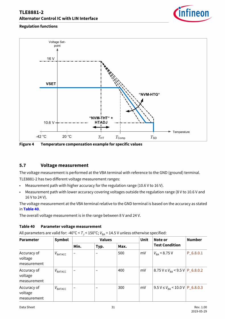
5.6 Temperature Setpoint Compensation (TSC)The temperature compensation gradually decreases the voltage setpoint (VSET) based on the measuredjunction temperature of the device. To compensate the produced energy at the excitation output stage, VSETis decreased at higher temperatures.The behavior of the temperature compensation in normal operation can be adjusted via EEPROM and LINframes. Figure 4 shows the behavior including the influence factors of the two parameters THT and the high-temperature gradient HTG.THT is the high-temperature threshold from where the temperature compensation would be activated if thevoltage setpoint is set to 16 V. THT can be adjusted in EEPROM via NVM field NVM-THT and via HTADJ(modifiable via RHT register in LIN RX frame). The adjustment via EEPROM is an absolute threshold value,whereas the adjustment via LIN adds a relative offset (positive or negative) to the EEPROM adjustment of theabsolute threshold value. NVM-HTG defines the gradient of the temperature compensation phase for thevoltage setpoint of 16 V.The temperature compensation is activated as soon as the actual VSET intersects with the gradient HTG -intersection point is called TCOMP. Calculation of TCOMP (as shown in Figure 4), is stated in Equation (5.1)
(5.1)
The lower the HTG gradient, the later the compensation will be activated. The higher the actual voltagesetpoint, the earlier the compensation will be activated.As soon as TJ > TCOMP, the high-temperature diagnostic flag (F-HT) is set to 1.
Table 39 Parameter temperature measurementsAll parameters are valid for: -40°C < TJ < 150°C; VBA = 14.5 V, unless otherwise specified:
Parameter Symbol Values Unit Note or Test Condition NumberMin. Typ. Max.
Temperature rise/fall gradient
TFRF – 28 – K/s Used in normal operation, default operation
P_6.6.0.1
Junction temperature measurement tolerance
ΔTJ -10 – +10 K – P_6.6.0.2
Junction temperature measurement tolerance
ΔTJ -5 – +5 K Device in “ComActive” at 25°C ambient temperature1)
1) Only wafer test
P_6.6.0.3
VSET - 16 V“NVM-HTG“
TComp = “NVM-THT“ + HTADJ +
Data Sheet 31 Rev. 1.00 2019-05-29
TLE8881-2Alternator Control IC with LIN Interface
Regulation functions
Figure 4 Temperature compensation example for specific values
5.7 Voltage measurementThe voltage measurement is performed at the VBA terminal with reference to the GND (ground) terminal.TLE8881-2 has two different voltage measurement ranges: • Measurement path with higher accuracy for the regulation range (10.6 V to 16 V).• Measurement path with lower accuracy covering voltages outside the regulation range (8 V to 10.6 V and
16 V to 24 V).The voltage measurement at the VBA terminal relative to the GND terminal is based on the accuracy as statedin Table 40. The overall voltage measurement is in the range between 8 V and 24 V.
Table 40 Parameter voltage measurementAll parameters are valid for: -40°C < TJ < 150°C; VBA = 14.5 V unless otherwise specified:
Parameter Symbol Values Unit Note or Test Condition
NumberMin. Typ. Max.
Accuracy of voltage measurement
VBATACC – – 500 mV VBA < 8.75 V P_6.8.0.1
Accuracy of voltage measurement
VBATACC – – 400 mV 8.75 V ≤ VBA < 9.5 V P_6.8.0.2
Accuracy of voltage measurement
VBATACC – – 300 mV 9.5 V ≤ VBA < 10.0 V P_6.8.0.3
Temperature
TSD
Voltage Set-point
16 V
10.6 V
“NVM-HTG“
20 °C-42 °C
VSET
THT
“NVM-THT“ + HTADJ
TComp

Data Sheet 32 Rev. 1.00 2019-05-29
TLE8881-2Alternator Control IC with LIN Interface
Regulation functions
5.8 Speed measurementThe measurable speed is limited in the range from 500 rpm to 25500 rpm. The determination of the speed isdone by measuring the frequency of the signal at the phase terminal and normalizing to the alternator polepairs (NVM field NVM-PP).The speed measurement is only available in the normal operation state.The representation of the speed measurement value is based on the accuracy as stated in Table 41 and on theregister resolution (capability of lowest significant bits).
5.9 Low Voltage Excitation On (LEO)At a very low battery voltage, loading of the excitation coil is immediately induced by providing the maximumexcitation current (excitation PWM duty cycle set to 100%) at the excitation output stage, until a definedthreshold (VLOW) is achieved. This feature is called Low-Voltage Excitation On (LEO).The enabling of the LEO function in normal mode depends on the NVM-LEOTIMERdis. If the NVM-LEOTIMERdis = 1B, the LEO function is enabled immediately after the Normal Operation is entered.If the LEO function gets activated, the excitation PWM duty cycle is set to 100%.If the NVM-LEOTIMERdis = 0B, a timer is started when VBA exceeds VLOW. If VBA falls below VLOW while the timer is running, the timer is reset and starts to run as soon as VBA exceeds VLOWagain.
Accuracy of voltage measurement
VBATACC – – 250 mV 10.0 V ≤ VBA < 10.5 V
P_6.8.0.4
Accuracy of voltage measurement
VBATACC – – 200 mV 10.5 V ≤ VBA < 16.0 V
P_6.8.0.5
Accuracy of voltage measurement
VBATACC – – 400 mV 16 V ≤ VBA ≤ 16.5 V P_6.8.0.6
Accuracy of voltage measurement
VBATACC – – 700 mV 16.5 V < VBA ≤ 24 V P_6.8.0.7
Table 41 Parameter speed measurementAll parameters are valid for: -40°C < TJ < 150°C; VBA = 14.5 V unless otherwise specified:
Parameter Symbol Values Unit Note or Test Condition
NumberMin. Typ. Max.
Accuracy of speed measurement
wmeasACC – 10 – % 1)
1) Not subject to production test.
P_6.9.0.1
Table 40 Parameter voltage measurement (cont’d)All parameters are valid for: -40°C < TJ < 150°C; VBA = 14.5 V unless otherwise specified:
Parameter Symbol Values Unit Note or Test Condition
NumberMin. Typ. Max.

Data Sheet 33 Rev. 1.00 2019-05-29
TLE8881-2Alternator Control IC with LIN Interface
Regulation functions
If VBA stays above VLOW during the runtime of the timer, the LEO function is enabled when the timer expires aftertLEODEL.While LEO function is activated, the F-EL will be set with the respective debounce time, if NVM field NVM-LEO_ERR_EN set to 1B.While the LEO function is enabled, the regulation loop as well as any LRC ramp (Load Response Controlspecified in Chapter 5.12) continue their regular operation in the background.The behavior after deactivating the LEO function (VBA > VLOW) can be selected via NVM-LEOLRC. The TLE8881-2 will set the LRC value to 100% DC , if NVM-LEOLRC = 0B, or stays at the actual value if NVM-LEOLRC = 1B.LEO is not available for all states (refer to Table 9). For longer LEO periods the DC can be reduced for one PWMperiod in order to conduct a current measurement as mentioned in Chapter 5.3.
Table 42 Parameter low-voltage excitation onAll parameters are valid for: -40°C < TJ < 150°C; unless otherwise specified:
Parameter Symbol Values Unit Note or Test Condition
NumberMin. Typ. Max.
LEO threshold VLOW 8.25 8.75 9.15 V 1);NVM field NVM-LEO = 000B;
P_6.10.0.1
LEO threshold VLOW 8.6 9 9.4 V 1);NVM field NVM-LEO = 001B
P_6.10.0.2
LEO threshold VLOW 8.85 9.25 9.65 V 1);NVM field NVM-LEO = 010B
P_6.10.0.3
LEO threshold VLOW 9.2 9.5 9.8 V 1);NVM field NVM-LEO = 011B
P_6.10.0.4
LEO threshold VLOW 9.45 9.75 10.05 V 1);NVM field NVM-LEO = 100B
P_6.10.0.5
LEO threshold VLOW 9.75 10.0 10.25 V 1);NVM field NVM-LEO = 101B
P_6.10.0.6
LEO threshold VLOW 10 10.25 10.5 V 1);NVM field NVM-LEO = 110B
P_6.10.0.7

Data Sheet 34 Rev. 1.00 2019-05-29
TLE8881-2Alternator Control IC with LIN Interface
Regulation functions
5.10 High Voltage Excitation Off (HEO)At overshooting above a very high on-board power supply voltage level (VHIGH), the excitation output stage isimmediately disabled (lock to DMOS switch-off). As soon as the voltage level is below this threshold, the DMOSlock is released (DMOS can switch-on and switch-off as requested by regulation loop). This feature is calledHigh-Voltage Excitation Off (HEO). HEO is a safety feature to switch-off the excitation output stage at dangerous high voltage levels (e.g. causedby load dump in the on-board power supply). This feature has the highest priority above all other functionsand is not available in all operation states (refer to Table 9).The HEO threshold, VHIGH, is stated in Table 43.The analogue HEO function can be activated/deactivated by NVM-HEO_ANdis. It is working independentlyparallel to the regular HEO function. It is not displayed with a LIN flag.
LEO threshold VLOW 10.3 10.5 10.7 V 1);NVM field NVM-LEO = 111B
P_6.10.0.8
LEO enable timer (VBA > VLOW)
tLEODEL 425 475 525 ms 1);If NVM-LEOTIMERdis = 0B;Timer initiated after transition from Pre-Excitation to Normal Operation state
P_6.10.0.10
1) Not subject to production test, specified by design and functional test.
Table 43 Parameter High Voltage Excitation OFFAll parameters are valid for: -40°C < TJ < 150°C; VBA=14.5 V unless otherwise specified:
Parameter Symbol Values Unit Note or Test Condition NumberMin. Typ. Max.
High-battery voltage threshold
VHIGH 16.1 16.5 16.9 V 1) P_6.11.0.1
Table 42 Parameter low-voltage excitation on (cont’d)All parameters are valid for: -40°C < TJ < 150°C; unless otherwise specified:
Parameter Symbol Values Unit Note or Test Condition
NumberMin. Typ. Max.

Data Sheet 35 Rev. 1.00 2019-05-29
TLE8881-2Alternator Control IC with LIN Interface
Regulation functions
Analogue HEO activation voltage threshold
VHIGHan,en 16.4 17.4 18.7 V Operating in parallel to digitally implemented Over-Voltage Excitationoff if NVM-HEO_ANdis = 0B
P_6.11.0.2
Analogue HEO deactivation voltage threshold
VHIGHan,dis 16.3 17.4 18.6 V Operating in parallel to digitally implemented Over-Voltage Excitationoff if NVM-HEO_ANdis = 0B
P_5.11.0.1
1) Not subject to production test.
Table 43 Parameter High Voltage Excitation OFF (cont’d)All parameters are valid for: -40°C < TJ < 150°C; VBA=14.5 V unless otherwise specified:
Parameter Symbol Values Unit Note or Test Condition NumberMin. Typ. Max.

Data Sheet 36 Rev. 1.00 2019-05-29
TLE8881-2Alternator Control IC with LIN Interface
Regulation functions
5.11 Phase Signal Boost (PSB)Phase Signal Boost (PSB) is an essential function to maintain a proper phase signal detection.
Conditions and behaviorThe PSB is activated by default within the respective states (see Table 9). Deactivation will happen beyondthose states. Enabling and disabling conditions as well as the behavior of the PSB function is described in thefollowing.The PSB function is activated if the upper peak voltage of VPH is below the upper deactivation level or the lowerpeak voltage of VPH is above the lower deactivation level.The PSB function is deactivated if the upper peak voltage of VPH is above the upper deactivation level and thelower peak voltage of VPH is below the lower deactivation level.If the PSB Function is activated the EXC output is set to 100% duty cycle for the PSB ON-time. If the PSB Function is activated the EXC output is set to 0% duty cycle during the PSB OFF-time.If the PSB function is active for longer than tPSB,ON+tPSB,OFF, a “PSB error” event (Trigger condition: PSB enabledfor longer than 1 PSB period) is emitted and an F-EL event is triggered (see Chapter 4.5).For the prioritization of different functions and their availability in different states see Table 9.
5.12 Load Response Control (LRC)Load Response Control (LRC) prevents engine speed hunting and vibration due to electrical loads which causeabrupt torque loading of the engine at lower speeds. This prevention is achieved by limiting the rise gradientof the excitation PWM duty cycle at the output stage.
Table 44 Parameter phase signal boost timerAll parameters are valid for: -40°C < TJ < 150°C; VBA = 14.5 V unless otherwise specified:
Parameter Symbol Values Unit Note or Test Condition NumberMin. Typ. Max.
Minimum required phase voltage level for PSB activation
VPSB,on,min 0.4 1 1.3 V PSB is enabled as soon as phase voltage level (VPH) goes below the specified voltage level
P_6.12.0.1
Maximum required phase voltage level for PSB activation
VPSB,on,max 6.1 7 7.6 V PSB is enabled as soon as phase voltage level (VPH) overshoots the specified voltage level
P_6.12.0.2
ON time for PSB tPSB,ON Typical value -10%
Typ. value
Typical value +10%
ms 1);Typ. value depends on NVM register NVM-T_PSB_ON_MAX
1) Not subject to production test.
P_6.12.0.3
OFF time for PSB tPSB,OFF 253 282 311 ms 1) P_6.12.0.4

Data Sheet 37 Rev. 1.00 2019-05-29
TLE8881-2Alternator Control IC with LIN Interface
Regulation functions
Figure 5 Principle of load response control
If the LRC function is disabled, the targeted Duty Cycle (DC) will be directly set to the regulator output value.If the LRC function is enabled and the targeted DC of the internal regulator is higher than the sum of currentDC and LRC blind-zone value, the LRC function applies a rising gradient to the duty cycle of the excitationOutput Stage.The LRC blind-zone restrains the application of the LRC function for a defined range of DC changes. Thisprevents a continuous applied rise gradient of the DC especially for small DC changes and assures a betterdynamic behavior.If the LRC function is enabled and the targeted DC of the internal regulator is lower than the subtraction ofcurrent DC and LRC blind-zone value, the LRC function internally calculates a falling gradient which is notapplied to the excitation Output Stage and therefore not seen at the excitation DMOS. This internallycalculated falling gradient is used as the starting point for next re-application of a LRC rising gradient (e.g. thetargeted DC is higher than the sum of the current DC and the LRC blind-zone value). This assures a betterdynamic behavior.Behavior of the LRC function after special conditions:• If the state of the IC is restored to normal operation after an inadvertent reset, the LRC value is set to 100%.• The behavior of the LRC function after an LEO event can be programmed by NVM-LEOLRC.
Once LEO is deactivated, the LRC value is set to 100% if NVM-LEOLRC = 0B or stays at the actual value if NVM-LEOLRC = 1B
The principle of LRC and the LRC blind-zone is shown in Figure 5.
LRC rise-time (LRCRT)The rising gradient is given by the LRC rise time (parameter LRCRT). This parameter can be configured via LINRX frames (RB in Data Byte 2, refer to Chapter 6.3.3) and in NVM via NVM-LRCRT for default operation. TheLRC rise-time is defined as the ramp-up time to go from 0% to 100% DC value, while the LRC function isactivated (nR < nLRCDIS and the positive DC change exceeds LRC blind-zone).
LRC active
Duty cycle[%]
(seen at output DMOS)
DC + α
DC
Sample time [τ]
“Blind-zone“
No LRC enabledNo LRC enabled No LRC enabled
DC τ
+1<
DC τ
+ α
DCτ+
1>
DCτ
+ α
Blind-zone leftLRC activated
(rising gradient)

Data Sheet 38 Rev. 1.00 2019-05-29
TLE8881-2Alternator Control IC with LIN Interface
Regulation functions
LRC fall-time (LRCFT)The falling gradient is given by the LRC fall time (parameter LRCFT). In contrast to LRCRT, this parameter canonly be configured in NVM via NVM-LRCFT. It is defined as the ramp down time to go from 100% to 0% DCvalue, while the LRC function is activated (nR < nLRCDIS).
LRC blind-zone (LRCBZ) The blind-zone is defined as the DC range, where the LRC function will not be activated. In case of a DC changewhich is higher than the blind-zone value (in percent of current DC), the LRC function will be activated for thisDC change. This parameter can be configured via NVM-LRCBZ and NVM-LRCBZ_0_SEL.
LRC disable speed (LRCDIS)If the measured rotor speed is high, the applied engine torque can be strong enough to overcome speed-hunting and vibration due to a DC change. Therefore, the LRC disable speed can deactivate the LRC dependingon the rotor speed, if nR > nLRCDIS.This parameter can be configured via LIN RX frames (RC in Data Byte 2) and for the default mode in NVM viaNVM-LRCDIS.
In summary, the LRC function is disabled in one or more of the following cases:• nR > nLRCDIS and TLE8881-2 register RLRCDIS is not 1111B.• TLE8881-2 register RLRCRT = 0000B.If the LRC is enabled by change of the registers LRCRT or LRCDIS, the limitation value starts on the actualexcitation duty cycle value.
5.13 Frequency-dependent Excitation Current Limitation (FEXLIM)Preventing higher torque loads especially for low temperature ranges as well as preventing heat-up due tohigh current flow is an important protection feature. The Frequency-dependent Excitation Current Limitation(FEXLIM) feature provides the possibility to adjust the limit of the excitation current depending on themeasured rotation speed of the alternator pulley.The FEXLIM feature limits the excitation current by adjusting the permanent current limitation (PCLIM) values.FEXLIM can operate in parallel to the excitation current limitation via LIN (Chapter 5.4), which limits theexcitation current by adjusting the RCLIM values (RCLIM register).
Table 45 Parameter Load Response Control (LRC)Parameter Symbol Values Unit Note or Test Condition Number
Min. Typ. Max.Blind zone BZdigital 3% 3% 4% - 1);
NVM-LRCBZ= 0B and NVM-LRCBZ_0_SEL= 0B
1) Not subject to production test. BZ is digitally implemented, so that the typical value can be targeted by design. Tolerances are related to DC changes on the middle of the PWM on-time.
P_6.13.0.1
Blind zone BZdigital 6.25% 6.25% 8% - 1); NVM-LRCBZ = 0B and NVM-LRCBZ_0_SEL= 1B
P_6.13.0.2
Blind zone BZdigital 12% 12% 14% - 1); NVM-LRCBZ = 1B
P_6.13.0.3

Data Sheet 39 Rev. 1.00 2019-05-29
TLE8881-2Alternator Control IC with LIN Interface
Regulation functions
By using the NVM bit field NVM-FEXLIM_EN in the EEPROM, the FEXLIM function can be enabled/disabled, seeTable 47.FEXLIM feature is available for all device configurations (VDA-A, VDA-B, OEM2 and OEM1).
5.13.1 Parameters and limitation areasThe frequency dependent current limitation (FEXLIM) has 2 limitation areas separated by a speed-dependentthreshold. This threshold is stated in Table 48.
Figure 6 shows an overview of the limitation areas and the adjustment options.
Figure 6 Principle of frequency-dependent current limitation overview of FEXLIM limitation areas and adjustment options (adjustments are red-highlighted, fixed values are black-contrasting)
5.13.2 Function activation/deactivationA dedicated switch in the NVM is provided to activate/deactivate the FEXLIM function, NVM-FEXLIM_EN.
5.13.3 FEXLIM vs. RCLIM register valueBeside the FEXLIM limitation values (as specified in Table 46 and Table 48), LIN commands can limit theexcitation current.
Table 46 Excitation current limitation values within the different limitation areasLimitation area Conditions PCLIM valueArea 1 nR < SLM PCLIM1
Area 4 SLM < nR PCLIM2
Table 47 Activation/deactivation switch for FEXLIM functionActivation/deactivation switch
Description Behavior
NVM-FEXLIM_EN = 0B Deactivate FEXLIM function CLIM (Excitation Current Limitation) is defined by the RCLIM register value via LIN only.
NVM-FEXLIM_EN = 1B Activate FEXLIM function CLIM (Excitation Current Limitation) is defined by the RCLIM register value via LIN and by PCLIM via the FEXLIM feature.
Speed [rpm]
Perm. Excitation
Current Limits [A]
(while RCLIM > PCLIMx)
NVM-FEXLIM_PCLIM2
SLM
NVM-FEXLIM_PCLIM1
Hysterisis SLM
Hysterisis SLM

Data Sheet 40 Rev. 1.00 2019-05-29
TLE8881-2Alternator Control IC with LIN Interface
Regulation functions
The LIN RX frame rewrites the RCLIM register value. The RCLIM register is used for applying the CLIM (ExcitationCurrent Limitation) within the normal operation state (refer to Chapter 5.4). While in parallel operation withFEXLIM, priorities have to be defined which actual limitation values will be used for CLIM.Depending on the case, the following value for CLIM will be applied while RCLIM (≠0) is provided:• If FEXLIM is enabled and RCLIM < PCLIM (as defined in Table 48), then CLIM is applied by RCLIM.• If FEXLIM is enabled and RCLIM > PCLIM, then CLIM is applied by PCLIM (as defined in Table 48).
Figure 7 Priorities between FEXLIM and RCLIM
5.13.4 Transition behaviorsSmooth transition ramps between different PCLIM values or RCLIM values avoid hunting or vibration due totorque changes.Any change of the PCLIM value over a speed threshold (e.g. PCLIM1 to PCLIM2 due to SLM threshold) will behandled by a smooth transition ramp, dtFSLOPE (static value of 0.375 A/s, refer to Table 48).Receiving of a RCLIM value which is different to the previous set RCLIM value can interrupt the transition ramp:• Positive transition slopes (transition from a lower to a higher limitation value) are interrupted if a new
RCLIM value is received. The new CLIM value to be adjusted for current limitation is defined by the static condition as described in Chapter 5.13.3 (The CLIM value is defined by the RCLIM value, if RCLIM < PCLIM, or the CLIM value is defined by PCLIM, if RCLIM > PCLIM).
• Negative transition slopes (transition from a higher to a lower limitation value) are interrupted if a new RCLIM value is received which is lower than the transient PCLIM value (current value on the transition ramp). The new CLIM value is defined by the received RCLIM value.
Note: “New RCLIM” refers to a RCLIM value received via an RX LIN-Frame which is different to the RCLIM value received by an earlier RX LIN-Frame.
If the state machine transfers from the normal to the default operation state and NVM-FEXLIM_EN = 0B(FEXLIM function deactivated), a smooth transition ramp, dtFSLOPE, from the last CLIM value to “no currentlimitation” (CLIM disabled) will be applied.
5.13.5 Function characteristicsTable 48 provides all related characteristics of the FEXLIM function.
Time [s]
CLIM [A]
PCLIM
RCLIM1
RCLIM2
„RCLIM2“ sent via LIN
„RCLIM1“ sent via LIN
„RCLIM disbaled“
sent via LIN
NVM-FEXLIM_EN = 0NVM-FEXLIM_EN = 1

Data Sheet 41 Rev. 1.00 2019-05-29
TLE8881-2Alternator Control IC with LIN Interface
Regulation functions
5.13.6 Behavior with restore state functionIn case of a restore state event (occurred due to micro-cut), the last PCLIM value can be restored. However, ifmicro-cuts occur during the drive of a transition slope, the targeted PCLIM value will be restored by the restorestate function. An exemplary behavior is represented in Figure 8.
Figure 8 Example of the behavior of FEXLIM on restore state event
Table 48 FEXLIM characteristicsAll parameters are valid for: -40°C < TJ < 150°C; VBA = 14.5 V, unless otherwise specified. All parameter are not subject to production tests.
Parameter Symbol Values Unit Note or Test Condition
NumberMin. Typ. Max.
Excitation current limitation for lower speed range
PCLIM1 – NVM-FEXLIM_PCLIM1 – A – P_6.14.5.3
Excitation current limitation for higher speed range
PCLIM2 – NVM-FEXLIM_PCLIM2 – A – P_6.14.5.4
Speed threshold SLM
SLM – 3400 – rpm Dependent on hysteresis. Actual value is SLM ± ΔSLM
P_6.14.5.7
Hysteresis SLM ΔSLM – 150 – rpm P_6.14.5.10
Transition ramp dtFSLOPE – 0.375 – A/s Slope between PCLIM1, PCLIM2. VDA-A / VDA-B / OEM1 / OEM2 variants.
P_6.14.5.12
Time [s]
PCLIM [A]
PCLIM1
PCLIM2
„nR > SLM“ event
VBA [V]
„Micro-cut“
Transition ramp

Data Sheet 42 Rev. 1.00 2019-05-29
TLE8881-2Alternator Control IC with LIN Interface
Regulation functions
5.14 Regulation parameters control via LIN (F-Para function)The TLE8881-2 makes use of a full digital PI regulator to control the excitation output stage. Both the Ki andthe Kp parameter are significant factors for the regulation dynamic. Since the regulation dynamic may change depending on the application circumstances, the TLE8881-2 offersfunctionalities to change the set of regulation parameters.The TLE8881-2 offers the F-Para functionality for switching from the normal KiKp setting to a previouslyselected regulation parameter set by setting a dedicated bit in the LIN RX frame. As long as that LIN bit is set,the PI regulator uses that pre-selected set of Ki and Kp factors. As soon as the LIN bit is reset, the default Ki andKp factors are used again. The pre-selection is adjusted by the NVM field NVM-RPARA_SEL.The pre-selection offers the possibility to either adjust a lower regulation dynamic or to not change theregulation dynamic. The pre-selected regulation parameter can be activated by the ECU via LIN data field RH in the LIN RX frame(Chapter 6.3.3).
5.15 Speed-dependent KiKp parameter sets (KiKp function)The TLE8881-2 allows to use different regulation KiKp parameter sets for the regulation of the EXC duty cycledependent on the rotation speed nR of the alternator.The device provides 4 different KiKp parameter sets fixed which can be selected:• “Normal” (default parameter)• “slow”• “slower”• “slowest”The name of the parameter sets is derived from the reaction speed of the regulation.The behavior of the function is configured by the parameter NVM-KiKp. This is shown in Table 49.
The function can be operated as a simple KiKp function or a 3-stage KiKp described in Figure 9 and Figure 10
Figure 9 Simple KiKp function
Table 49 Configuration of KiKp functionConfiguration switch DescriptionNVM-KiKp= 00B KiKp function disabled
NVM-KiKp = 01B Simple KiKp function with KiKp set to “slowest”
NVM-KiKp = 10B Simple KiKp function with KiKp set to “slower”
NVM-KiKp = 11B 3-stage KiKp function
Nswitch1 N[RPM]
Regelution
Slower or slowest
KiKp active

Data Sheet 43 Rev. 1.00 2019-05-29
TLE8881-2Alternator Control IC with LIN Interface
Regulation functions
Figure 10 3-stage KiKp function
The selection of the different KiKp parameter sets is done based on the rotation speed nR. The function allowsup to 3 different speed thresholds Nswitch1.... Nswitch3.These thresholds can be selected by the parameter NVM-Speed_TH(see Table 50). The table shows the upperthreshold and the lower threshold for the implemented hysteresis.The change of the used KiKp parameter set is triggered by a KiKp Nswitch event. The criteria for this event areshown in Table 51.
If the F-Para function is not active (set to 0 in the LIN-RX frame) and the KiKp function is activated in NVM-KiKp,the KiKp parameters requested by the KiKp function are applied.
Table 50 Selection of Nswitch speed thresholds1)
1) 2000 / 1800 rpm represent the upper and lower value of the hysteresis
NVM-Speed_TH Nswitch1 [rpm] Nswitch2 [rpm] Nswitch3 [rpm]000B 2000 / 1800 2400 / 2200 2800 / 2600
001B 2200 / 2000 2600 / 2400 3000 / 2800
010B 2400 / 2200 2800 / 2600 3200 / 3000
011B 2600 / 2400 3000 / 2800 3400 / 3200
100B 2800 / 2600 3200 / 3000 3600 / 3400
101B 3000 / 2800 3400 / 3200 3800 / 3600
110B 3200 / 3000 3600 / 3400 4000 / 3800
111B 3400 / 3200 3800 / 3600 4200 / 4000
Table 51 KiKp Nswitch events and conditionsEvent Description Set condition
(event is generated)
Clear condition(event is cleared)
“KiKp Nswitch” event
Event used to trigger the selection of the KiKp parameter sets
3 consecutive measurements with nR > Nswitch(upper threshold of hysteresis)
3 consecutive measurements with nR < Nswitch(lower threshold of hysteresis)
Nswitch1 N[RPM]
slowestslower
slownormal
Regulation
Nswitch2 Nswitch3
KiKp active

Data Sheet 44 Rev. 1.00 2019-05-29
TLE8881-2Alternator Control IC with LIN Interface
Regulation functions
If the F-Para function is not active (set to 0 in the LIN-RX frame) and the KiKp function is not activated, thenormal regulation parameters are applied. If the F-Para function is active (set to 1 in the LIN-RX frame), the parameters requested by the F-Para functionare applied.
5.16 Voltage-dependent KiKp function (VoKiKp function)In order to avoid slow reaction of the IC on relatively high VBA voltages compared to VSET, especially if slowKiKp parameter sets are chosen, the TLE8881-2 offers a voltage-dependent KiKp function (VoKiKp).
The function and its parameters can be selected by the NVM parameter NVM-VoKiKp shown in Table 52
If the VoKiKp function is active, it overrules the KiKp parameter set selection performed by the F-Para functionor the KiKp function and forces the IC to use the KiKp parameter set “Normal”.The activation and deactivation of the function is shown in Figure 11. The function is activated if VBA is higher than VSET + VoKiKp up threshold and deactivated if VBA is lower thanVSET + VoKiKp down threshold. For the values 101B, 110B and 111B the function is also activated if VBA is lowerthan VSET - VoKiKp up threshold and deactivated if VBA is higher than VSET - VoKiKp down threshold.
Figure 11 Voltage-dependent activation and deactivation of the VoKiKp function.
Table 52 Configuration of VoKiKp functionNVM-VoKiKp VoKiKp up threshold VoKiKp down threshold000B VoKiKp disabled
001B 0.35 V 0.25 V
010B 0.5 V 0.4 V
011B 0.65 V 0.55 V
100B 0.8 V 0.7 V
101B +/- 0.5 V +/- 0.4 V
110B +/- 0.75 V +/- 0.65 V
111B +/- 1 V +/- 0.9 V
t
VBa Measured voltage
t
VoKiKp_upVoKiKp_ down
Vset
VoKiKp_active

Data Sheet 45 Rev. 1.00 2019-05-29
TLE8881-2Alternator Control IC with LIN Interface
Regulation functions
The VoKiKp function is deactivated as well if the rotation speed is high. The deactivation threshold dependson the KiKp configuration (Table 49).If the simple KiKp function is used or if the KiKp function is disabled, the VoKiKp function is deactivated ifnR > Nswitch1.If the three stage KiKp function is used the VoKiKp function is deactivated if nR > Nswitch3.The speed dependence of the VoKiKp function can be activated/deactivated by the NVM parameter NVM-VoKiKp_low_HEO_speed.

Data Sheet 46 Rev. 1.00 2019-05-29
TLE8881-2Alternator Control IC with LIN Interface
Regulation functions
5.17 Speed-dependent lowering of the HEO limit (LowHEO function)In order to optimize the reaction to high VBA voltages in case of a low rotation speed, the TLE8881-2 offers afunction to lower the HEO limit. This function is called LowHEO function.
The function and its parameters can be selected by the NVM parameter NVM-LOW_HEO shown in Table 53
If the rotation speed nR is lower than Nswitch1, the HEO limit is reduced to the preconfigured value set in theNVM parameter NVM-LOW_HEO.In this situation, the VSET voltage is limited to the lower HEO limit -500 mV. The LowHEO function will trigger the F-EL diagnostic flag if nR < Nswitch1 and the battery voltage is higher thanthe LowHEO voltage.The speed dependence of the LowHEO function can be activated/deactivated by the NVM parameter NVM-VoKiKp_low_HEO_speed. If the speed dependence is disabled, NVM-LOW_HEO is applied for all rotationspeeds.For example, if the lower HEO limit is set to 15.5 V, the VSET voltage is limited to 15 V.This function is shown in Figure 12.
Figure 12 Speed-dependent lowering of the HEO limit
Table 53 Configuration of the lowHEO functionNVM-LOW_HEO LowHEO voltage VLowHEO
00B 15.5 V
01B 15.65 V
10B 15.75 V
11B LowHEO function disabled (default HEO 16.5 V used)
Nswitch1 N[RPM]
HEO voltage
16.5VLow-HEO

Data Sheet 47 Rev. 1.00 2019-05-29
TLE8881-2Alternator Control IC with LIN Interface
LIN interface
6 LIN interfaceThe protocol of the TLE8881-2 communication interface is implemented as LIN bus according to the LIN (LocalInterconnect Network) specification. The physical layer is implemented according to the standard LIN 2.1specification. The physical layer specification LIN 2.1 is a super set of previous LIN specifications, such asversions of LIN 2.0 or LIN 1.3.The TLE8881-2 is qualified according to LIN 2.1 on the physical layer. Conformance test results are availableon request.The data link layer is implemented according to LIN 1.3 as well as LIN 2.1 specification (selectable via NVM-LIN).The data exchange via the serial bi-directional LIN bus line follows the master-slave-principle, where theengine management ECU or the energy management ECU is arranged as master (LIN 1.3, or LIN 2.1) and theTLE8881-2 is designed as a slave node.
6.1 Bus topologyThe LIN bus line is connected to the LIN terminal of the TLE8881-2 and to any driver/receiver of the busconnection. VSUP is an internal voltage and supplies the pull-up resistor of the LIN bus line. This voltage is usedfor the definition of the voltage thresholds. A polarity protection diode between VSUP and VBA is described inthe LIN standard and may be implemented in the LIN master. The TLE8881-2 uses an active polarity protectiondiode which is shorted in operational mode. Therefore, VSUP is more or less equal to VBA.While in stand-by mode a wake-up circuitry detects signal pulses on the LIN bus line. If a pulse fulfills the wake-up pulse requirement, the TLE8881-2 will leave the stand-by mode and changes to ComActive state.The LIN terminal of the TLE8881-2 is protected against short circuit to the GND terminal or VBA terminal. TheLIN driver is protected against overload.
Figure 13 LIN bus configuration
LIN-BUS
VBA
LIN-RXD
RLIN
Alternator IC - LIN 1.3/2.1 Slave(acc. to LIN 2.1 PL Spec)
Internal logic
GND
LIN
GND´
VBA´
ECU - LIN 1.3/2.1 Master
LIN-Tranceiver
RXD
TXD
VSUP,Master
1kΩ
Other LIN Slaves (second alternator)
CLIN
INH
LIN
VSUP
ILIN
Ground shift voltage(specified in LIN 2.1 PL)
Battery shift voltage(specified in LIN 2.1 PL)
VLIN
Closed when not in Stand-By
VLIN
Wake-up filter
Edge detection
LIN-TXD

Data Sheet 48 Rev. 1.00 2019-05-29
TLE8881-2Alternator Control IC with LIN Interface
LIN interface
6.2 Signal specification (physical layer)The transferred data bits are encoded with the value ‘0’ (dominant level, bus line is clamped to GND) or ‘1’(recessive, bus voltage is near to VBA). For a correct transmission of a bit the bus voltage must be on therespective voltage level (dominant or recessive) at the bit sampling time of the receiver. Propagation delaysas well as slew rates according the LIN specification have to be considered (refer to Figure 14).
Figure 14 LIN signal specification
The LIN bus communication speed (within the specified limits) is automatically detected by the receiver usingthe Synch Byte of the header (for LIN 1.3 and for LIN 2.1). In addition to the associated start bit and stop bit,the Synch Byte is coded as 55H (refer to Figure 15).The falling curve of the bus voltage VLIN (bit change from recessive to dominant) is mainly dependent on thedriver implementation, while the rising curve of the bus voltage (bit change dominant to recessive) dependson the bus time constant tLIN = RLIN x CLIN. The bus time constant, tLIN, has to be between 1 μs and 5 μs.RLIN is the overall network impedance and its value is depending on the number of bus nodes. Because thenumber of nodes should not exceed a maximum of 16, the minimum value is never below RLIN = 500 Ω. CLIN isthe overall network capacitance and must not exceed 10 nF.CLIN is the overall network capacity and consists of the master capacity, slave node capacities as well as buswire length.For more details concerning the bus line timing and characteristics, refer to the LIN 2.1 specification.
VSUP
Recessive
Dominant
GNDt
t
VLIN
LIN-TXD
0,6 x VSUP
0,4 x VSUP
VLIN,cnt
LIN-RXD
VLIN,d2r
VLIN,r2d
tRXPDF tRXPDR
tBus_dom
TBIT TBIT TBIT
VBAT
t
Voltage drop over the diodes in pull-up pathtBus_rec

Data Sheet 49 Rev. 1.00 2019-05-29
TLE8881-2Alternator Control IC with LIN Interface
LIN interface
Table 54 Parameter LIN signal characteristicsAll parameters are valid for: -40°C < TJ < 150°C; VBA = 14.5 V, unless otherwise specified:
Parameter Symbol Values Unit Note or Test Condition NumberMin. Typ. Max.
Receiver input voltage for proper communication
VLIN -3 – 40 V Negative voltages could occur in case of ground shift between master and slave1)
P_7.2.0.1
Bit period TBIT 51 – 423 μs For LIN master: communication speed between 2400 bit/s and 19200 bit/s (master clock tolerance ± 0.5%)
P_7.2.0.2
Bit period TBIT 50 – 432 μs For TLE8881-2 slave node: maximum clock tolerance for communication between master and slave after synchronization is ± 2%
P_7.2.0.3
Interbyte delay in response
tBDEL – 0 – μs TLE8881-2 is sending the response immediately
P_7.2.0.4
Bus dominant time for the synch-break
tSYNBRK 13x TBIT – μs TBIT is the bit time ascertained in the synch-byte. Only whole-numbered (integer) multiples of TBIT are applicable.
P_7.2.0.5
Bus idle time-out tLINIDLE – 1300 – ms tLINIDLE (25k x TBIT @ 19200 bit/s) only used for LIN 2.1 conformance test
P_7.2.0.6
Internal voltage for bus pull-up resistor supply
VSUP VBA -1 V – VBA V 1); maximum voltage drop (current dependent) on internal polarity protection diode is 1 V
P_7.2.0.7
Receiver voltage threshold for bit recessive to bit dominant detection
VLIN,r2d 0.4xVSUP
– – V LIN 2.1 Param 17 (Figure 6.2) P_7.2.0.8
Receiver voltage threshold for bit dominant to bit recessive detection
VLIN,d2r – – 0.6xVSUP
V LIN 2.1 Param 18 (Figure 6.2) P_7.2.0.9
Receiver center voltage
VLIN,cnt 0.475xVSUP
0.5xVSUP
0.525xVSUP
V LIN 2.1 Param 19 (Figure 6.2) P_7.2.0.10
Receiver hysteresis VLIN,hys 0.07xVSUP
0.1xVSUP
0.175xVSUP
V VLIN,hys = VLIN,d2r - VLIN,r2dLIN 2.1 Param 20
P_7.2.0.11
LIN wake-up threshold voltage
VLINWK 0.4xVSUP
– 0.6xVSUP
V – P_7.2.0.12
Bus dominant time for LIN wake-up
tLINWK 30 – 150 μs – P_7.2.0.13

Data Sheet 50 Rev. 1.00 2019-05-29
TLE8881-2Alternator Control IC with LIN Interface
LIN interface
Bus current limitation for dominant stat
ILINMAX 40 – 200 mA In full VBA range;LIN 2.1 Param 12
P_7.2.0.14
Bus leakage current ILINLEAK -1 – – mA LIN-TXD = 1 (pull-down driver off), VLIN = 0 V, VBA = 12 VLIN 2.1 Param 13
P_7.2.0.15
Bus leakage current(loss of ground)
ILINLEAK -1 – 1 mA VLIN = -18 V to 0 VGND open on TLE8881-2;LIN 2.1 Param 15
P_7.2.0.16
Bus leakage current(loss of battery)
ILINLEAK – – 20 μA VLIN = 0 V to 18 VVBA open on TLE8881-2;LIN 2.1 Param 16
P_7.2.0.17
Bus leakage current(driver off)
ILINLEAK – – 20 μA VLIN = 8 V to 18 VVBA = 8 V to 18 VVLIN > VBALIN 2.1 Param 14
P_7.2.0.18
Voltage drop on serial diode in pull up resistor path
VLINDPU 0.4 – 1 V VBA = 6 V to 18 V, VLIN = 2 V
P_7.2.0.19
Pull-up resistor for LIN slave node
RLIN,Slave 20 30 60 kΩ LIN 2.1 Param 26 P_7.2.0.20
Internal capacity for LIN slave node
CLIN.Slave 10 – 80 pF 1) LIN 2.1 Param 37
P_7.2.0.21
LIN bus duty cycleD1 for 20 kbit/s
DCLIN 0.396 – – – 1) 2) 3)
LIN 2.1 Param 27P_7.2.0.22
LIN bus duty cycleD2 for 20 kbit/s
DCLIN – – 0.581 – 1) 2) 4)
LIN 2.1 Param 28P_7.2.0.23
LIN bus duty cycleD3 for 10.4 kbit/s
DCLIN 0.417 – – 1) 2) 5)
LIN 2.1 Param 29P_7.2.0.24
LIN bus duty cycleD4 for 10.4 kbit/s
DCLIN – – 0.590 1) 2) 6)
LIN 2.1 Param 30P_7.2.0.25
Rising receiver propagation delay
tRXPDR – – 6 μs 7)
LIN 2.1 Param 31P_7.2.0.26
Falling receiver propagation delay
tRXPDF – – 6 μs 7)
LIN 2.1 Param 31P_7.2.0.27
Receiver propagation delay symmetry (rising edge versus falling edge)
dtRXPD -2 – 2 μs 7)
LIN 2.1 Param 32P_7.2.0.28
Table 54 Parameter LIN signal characteristics (cont’d)All parameters are valid for: -40°C < TJ < 150°C; VBA = 14.5 V, unless otherwise specified:
Parameter Symbol Values Unit Note or Test Condition NumberMin. Typ. Max.

Data Sheet 51 Rev. 1.00 2019-05-29
TLE8881-2Alternator Control IC with LIN Interface
LIN interface
6.3 Message frames (data link layer)The TLE8881-2 can communicate with both a LIN 2.1 and a LIN 1.3 master. This is realized by implementingcalculations for both a classic checksum and an enhanced checksum. The selection of the supported LINprotocol can be adjusted via NVM-LIN.
Note: For backward compatibility reasons, a LIN 2.1 master is able to communicate with a LIN 1.3 slave but not vice versa. This backward compatibility is assured by the fact that the TLE8881-2 is designed according to LIN 2.1 on the physical layer, as recommended by the LIN consortium. Thus, and due to the NVM field switch, the TLE8881-2 can communicate with a master specified according to both LIN 2.1 as well as LIN 1.3.
Every data transfer is initiated from the master by sending a header. This header contains a synch-break field,a synch byte and a frame identifier byte (ID Byte, or labeled as Protected Identifier in the LIN 2.1 specification).The frame identifier byte defines the response which is sent by the master or the slave immediately after theLIN frame header. The response contains 1 to 8 data bytes as well as one checksum byte at the end of the LINframe. In the communication protocol of the TLE8881-2 only 2, 4 and 8 data bytes are defined as validresponses.Except for the synch-break field, LIN frames are byte-oriented so that the LIN specification allows a delaybetween bytes (interbyte delay). Every byte in a single LIN frame is composed of a start bit, 8 data bits and onestop bit. The bits are encoded with the value ‘0’ (dominant) or ‘1’ (recessive). In a bit stream of one data byte,the least significant bit (lsb) is indicated as the first arriving bit on the LIN bus, whereas the most significant bit(msb) is the last bit, respectively.Figure 15 shows a complete LIN frame for an identifier using 4 data bytes in the response field. The synch-break field re-initializes the receiver and marks the start of a new LIN frame in any case.
1) Not subject to production test.2) Bus loading conditions (CLIN;RLIN) = (1 nF;1 kΩ), (6.8 nF;660 Ω) and (10 nF;500 Ω). For signal specification, refer to
Figure 14 “LIN signal specification” on Page 48.3) VLIN,d2r = 0.744x VSUP, VLIN,r2d = 0.581x VSUP, VSUP = 7 V to 18 V, TBIT = 50 μs4) VLIN,d2r = 0.284x VSUP, VLIN,r2d = 0.422x VSUP, VSUP = 7.6 V to 18 V, TBIT = 50 μs5) VLIN,d2r = 0.778x VSUP, VLIN,r2d = 0.616x VSUP, VSUP = 7 V to 18 V, TBIT = 96 μs6) VLIN,d2r = 0.389x VSUP, VLIN,r2d = 0.251x VSUP, VSUP = 7 V to 18 V, TBIT = 96 μs7) Wafer Test only

Data Sheet 52 Rev. 1.00 2019-05-29
TLE8881-2Alternator Control IC with LIN Interface
LIN interface
Figure 15 LIN frame
If the bus is idle (recessive) for more than tLINIDLE, the receiver is re-initialized. That means that thesynchronization delimiter or any interbyte space must not exceed tLINIDLE of 25.000 bit times of 19200 baud,which is 1300 ms. Otherwise the frame is lost.The TLE8881-2 sends its response immediately after the identifier and it will not generate any delay betweenbytes in the response field (which results in no interbyte space).
6.3.1 LIN frame structure
Frame identifier byte / protected identifierOn principle, the LIN frame identifier byte (also know as the frame identifier field, or ID field) consists of 6identifier bits plus 2 parity bits. The coverage of having no pattern with all bits recessive or dominant can beguaranteed by the 2 parity bits inside the frame identifier field (ID field). The first parity bit is calculated by theXOR-concatenation between ID bits as indicated in Equation (6.1).
(6.1)
The second parity bit is computed by the inverse XOR-concatenation between ID bits as indicated inEquation (6.2).
(6.2)
Thus, the frame identifier byte never consists of 0’s or 1’s only and can be distinguished easily from the synch-break.
Synch Field ID Field Data1 Field Data2 Field Data3 Field Data4 FieldSynch-Break
Header - sent from Master (=ECU) Response - sent from Master (=ECU) or Slave (=Alternator Control IC)LIN Frame
ID Field
0 ID0 1
lsb msb
ID1 ID2 ID3 ID4 ID5 P0 P1
Frame Identifier Byte (= 00H to FFH)
Synch Byte (= 55H)
Synch Field
0 S0 S1 S2 S3 S4 S5 S6 S7 1
lsb msb
Synch-Break (min. 13x 0B)
Data Field - Data 1,2,4 or 8
0 D0 1
lsb msb
D1 D2 D3 D4 D4 D6 D7
Data Byte (= 00H to FFH)
Checksum Field
0 C0 1
lsb msb
C1 C2 C3 C4 C5 C6 C7
Checksum Byte (= 00H to FFH)
Synchronization delimiter (tSYNDEL)
tSYNBRK
Checksum Field
Interbyte space
ID0 ⊕ ID1 ID2⊕ ID4⊕ P0 =
ID1 ⊕ ID3 ID4⊕ ID5⊕ P1 =

Data Sheet 53 Rev. 1.00 2019-05-29
TLE8881-2Alternator Control IC with LIN Interface
LIN interface
Checksum byteFor the LIN 1.3 data link layer (EEPROM field NVM-LIN = 1B), a classic checksum calculation is used whichmeans inverting the sum of modulo 256 (with carry) of all data bytes. An eight bit sum with carry is equivalentto the sum of all values from which 255 is substracted every time the sum is greater, or equal to 256.For the LIN 2.1 data link layer (EEPROM field NVM-LIN = 0B), an enhanced checksum calculation is used whichadditionally includes the Protected Identifier Field (Identifier Byte including parity bits) in the sum of all databytes.According to the LIN specification, if the ID field is 3CH or 3DH, the classic checksum calculation will always beused.Examples for checksum calculation are given in the respective LIN specification documents.
Data byteEvery LIN frame is named with a unique symbol, starting with “R” for received frames (from the LIN master,also called request frames) and starting with “T” for transmitted frames (from the LIN master, also calledresponse frames). The “P” indicates fields or frames only used if test mode is active.TLE8881-2 supports the following data byte structures which can be chosen in NVM via NVM-CFG:• VDA-A variant• VDA-B variant• OEM1 variant • OEM2 variant
6.3.2 LIN frame identifier recommendationsThe TLE8881-2 supports the flexible configuration of the LIN Frame Identifiers. The identifiers can beconfigured via an EEPROM configuration of the fields NVM-LINRX, NVM-LINTX1, NVM-LINTX2, NVM-LINTX3(refer to Chapter 9.2.1). Table 55 provides recommended examples of the EEPROM configuration forreference purposes. Since the parity can be calculated via Equation (6.1) and Equation (6.2), the EEPROMconfiguration excludes the parity bits from the resulting byte.The LIN identifier for diagnostic frames is ignored for LIN 1.3 (NVM-LIN =1B) if NVM-3Ddis= 1B. If the TLE8881-2 is configured for LIN 2.1 (NVM-LIN=0B), it will send the specified response (see Chapter 6.7).The frames NVM-LINTX1, NVM-LINTX2 and NVM-LINTX3 can be deactivated by programming the frame ID inthe NVM to 0x3C. The TLE8881-2 will not answer to the TX frames and respond to 0x3C with the 0x3C diagnosticframe.
Table 55 LIN frame identifierTLE8881-2 config- uration
Symbol / comment
Identifier byte Data bytesIdentifier bits Parity Result
byteLength Sent by
Byte Bit0
Bit1
Bit2
Bit3
Bit4
Bit5
P0 P1
All1) Diagnostic frame (sleep command / programming)
3CH 0 0 1 1 1 1 0 0 3CH 8 Master
All Diagnostic frame 2)
3DH 1 0 1 1 1 1 1 0 7DH 8 TLE8881-2

Data Sheet 54 Rev. 1.00 2019-05-29
TLE8881-2Alternator Control IC with LIN Interface
LIN interface
VDA-A config for regulator #1
RX3) 29H 1 0 0 1 0 1 1 1 E9H 4 Master
TX1 11H 1 0 0 0 1 0 0 0 11H 2 TLE8881-2
TX2 12H 0 1 0 0 1 0 0 1 92H 2 TLE8881-2
TX33) 15H 1 0 1 0 1 0 1 0 55H 4 TLE8881-2
VDA-A config for regulator #24)
RX3) 2AH 0 1 0 1 0 1 1 0 6AH 4 Master
TX1 13H 1 1 0 0 1 0 1 1 D3H 2 TLE8881-2
TX2 14H 0 0 1 0 1 0 0 0 14H 2 TLE8881-2
TX33) 16H 0 1 1 0 1 0 1 1 D6H 4 TLE8881-2
OEM1 / VDA-B config for regulator #1
RX3) 29H 1 0 0 1 0 1 1 1 E9H 4 Master
TX1 - - - - - - - - - - -
TX2 12H 0 1 0 0 1 0 0 1 92H 2 TLE8881-2
TX33) 15H 1 0 1 0 1 0 1 0 55H 4 TLE8881-2
OEM1 / VDA-B config for regulator #24)
RX3) 2AH 0 1 0 1 0 1 1 0 6AH 4 Master
TX1 - - - - - - - - - - -
TX2 14H 0 0 1 0 1 0 0 0 14H 2 TLE8881-2
TX33) 16H 0 1 1 0 1 0 1 1 D6H 4 TLE8881-2
OEM2 config forregulator #1
RX3) 29H 1 0 0 1 0 1 1 1 E9H 4 Master
TX1 - - - - - - - - - - -
TX2 - - - - - - - - - - -
TX33) 21H 1 0 0 0 0 1 1 0 61H 4 TLE8881-2
OEM2 config forregulator #24)
RX3) 2AH 0 1 0 1 0 1 1 0 6AH 4 Master
TX1 - - - - - - - - - - -
TX2 - - - - - - - - - - -
TX33) 22H 0 1 0 0 0 1 1 1 E2H 4 TLE8881-2
TLE88815) config for regulator #1
RX3) 20H 0 0 0 0 0 1 0 0 20H 4 Master
TX1 15H 1 0 1 0 1 0 1 0 55H 2 TLE8881-2
TX2 21H 1 0 0 0 0 1 1 0 61H 2 TLE8881-2
TX33) 18H 0 0 0 1 1 0 1 1 D8H 4 TLE8881-2
TLE8881 config for regulator #24)
RX3) 2AH 0 1 0 1 0 1 1 0 6AH 4 Master
TX1 13H 1 1 0 0 1 0 1 1 D3H 2 TLE8881-2
TX2 11H 1 0 0 0 1 0 0 0 11H 2 TLE8881-2
TX33) 16H 0 1 1 0 1 0 1 1 D6H 4 TLE8881-21) The sleep mode command (ID byte = 3CH, data byte 1 = 00H) is only accepted by the TLE8881-2 in the states
“ComActive” and “pre-excitation”.2) LIN identifier ignored for LIN 1.3 (NVM-LIN = 1B AND NVM-3Ddis = 1B). LIN identifier responded by TLE8881-2 for LIN
2.1 (NVM-LIN = 0B).
Table 55 LIN frame identifier (cont’d)
TLE8881-2 config- uration
Symbol / comment
Identifier byte Data bytesIdentifier bits Parity Result
byteLength Sent by
Byte Bit0
Bit1
Bit2
Bit3
Bit4
Bit5
P0 P1
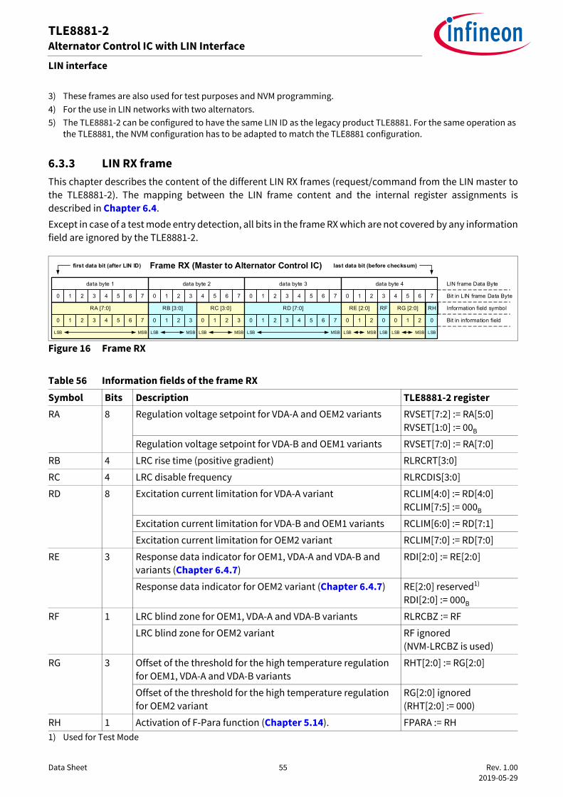
Data Sheet 55 Rev. 1.00 2019-05-29
TLE8881-2Alternator Control IC with LIN Interface
LIN interface
6.3.3 LIN RX frameThis chapter describes the content of the different LIN RX frames (request/command from the LIN master tothe TLE8881-2). The mapping between the LIN frame content and the internal register assignments isdescribed in Chapter 6.4.Except in case of a test mode entry detection, all bits in the frame RX which are not covered by any informationfield are ignored by the TLE8881-2.
Figure 16 Frame RX
3) These frames are also used for test purposes and NVM programming.4) For the use in LIN networks with two alternators.5) The TLE8881-2 can be configured to have the same LIN ID as the legacy product TLE8881. For the same operation as
the TLE8881, the NVM configuration has to be adapted to match the TLE8881 configuration.
Table 56 Information fields of the frame RXSymbol Bits Description TLE8881-2 registerRA 8 Regulation voltage setpoint for VDA-A and OEM2 variants RVSET[7:2] := RA[5:0]
RVSET[1:0] := 00B
Regulation voltage setpoint for VDA-B and OEM1 variants RVSET[7:0] := RA[7:0]
RB 4 LRC rise time (positive gradient) RLRCRT[3:0]
RC 4 LRC disable frequency RLRCDIS[3:0]
RD 8 Excitation current limitation for VDA-A variant RCLIM[4:0] := RD[4:0]RCLIM[7:5] := 000B
Excitation current limitation for VDA-B and OEM1 variants RCLIM[6:0] := RD[7:1]
Excitation current limitation for OEM2 variant RCLIM[7:0] := RD[7:0]
RE 3 Response data indicator for OEM1, VDA-A and VDA-B and variants (Chapter 6.4.7)
RDI[2:0] := RE[2:0]
Response data indicator for OEM2 variant (Chapter 6.4.7) RE[2:0] reserved1)
RDI[2:0] := 000B
1) Used for Test Mode
RF 1 LRC blind zone for OEM1, VDA-A and VDA-B variants RLRCBZ := RF
LRC blind zone for OEM2 variant RF ignored (NVM-LRCBZ is used)
RG 3 Offset of the threshold for the high temperature regulation for OEM1, VDA-A and VDA-B variants
RHT[2:0] := RG[2:0]
Offset of the threshold for the high temperature regulation for OEM2 variant
RG[2:0] ignored (RHT[2:0] := 000)
RH 1 Activation of F-Para function (Chapter 5.14). FPARA := RH
0 1 2 3 4 5 6 7 0 1 2 3 4 5 6 7 0 1 2 3 4 5 6 7 0 1 2 3 4 5 6 7
data byte 1 data byte 2 data byte 3 data byte 4 LIN frame Data Byte
Bit in LIN frame Data Byte
Information field symbol
Bit in information field
first data bit (after LIN ID) last data bit (before checksum)Frame RX (Master to Alternator Control IC)
RA [7:0]
0 1 2 3 4 5
RB [3:0]
0 1 2 3
RC [3:0]
0 1 2 3
MSBLSB MSBLSBMSBLSB
6 7
RD [7:0]
0 1 2 3 4 5
MSBLSB
6 7
RE [2:0]
0 1 2
MSBLSB
0
LSB
RF
0
LSB
RHRG [2:0]
0 1 2
MSBLSB
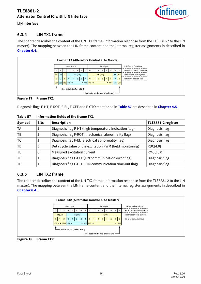
Data Sheet 56 Rev. 1.00 2019-05-29
TLE8881-2Alternator Control IC with LIN Interface
LIN interface
6.3.4 LIN TX1 frameThe chapter describes the content of the LIN TX1 frame (information response from the TLE8881-2 to the LINmaster). The mapping between the LIN frame content and the internal register assignments in described inChapter 6.4.
Figure 17 Frame TX1
Diagnosis flags F-HT, F-ROT, F-EL, F-CEF and F-CTO mentioned in Table 57 are described in Chapter 4.5.
6.3.5 LIN TX2 frameThe chapter describes the content of the LIN TX2 frame (information response from the TLE8881-2 to the LINmaster). The mapping between the LIN frame content and the internal register assignments in described inChapter 6.4.
Figure 18 Frame TX2
Table 57 Information fields of the frame TX1Symbol Bits Description TLE8881-2 registerTA 1 Diagnosis flag F-HT (high temperature indication flag) Diagnosis flag
TB 1 Diagnosis flag F-ROT (mechanical abnormality flag) Diagnosis flag
TC 1 Diagnosis flag F-EL (electrical abnormality flag) Diagnosis flag
TD 5 Duty cycle value of the excitation PWM (field monitoring) RDC[4:0]
TE 6 Measured excitation current RMC6[5:0]
TF 1 Diagnosis flag F-CEF (LIN communication error flag) Diagnosis flag
TG 1 Diagnosis flag F-CTO (LIN communication time-out flag) Diagnosis flag
0 1 2 3 4 5 6 7 0 1 2 3 4 5 6 7
data byte 1 data byte 2
first data bit (after LIN ID)
last data bit (before checksum)
Frame TX1 (Alternator Control IC to Master)
TE [5:0]
0 1 2 3 4
TA TB TC TD [4:0]
0 1 2 3 4 5
TF TG
MSBLSB MSBLSB
0 0 0
LSB LSB LSB
0 0
LSB LSB
LIN frame Data Byte
Bit in LIN frame Data Byte
Information field symbol
Bit in information field
0 1 2 3 4 5 6 7 0 1 2 3 4 5 6 7
data byte 1 data byte 2
first data bit (after LIN ID)
last data bit (before checksum)
Frame TX2 (Alternator Control IC to Master)
TJ [7:0]
0 1 2 3 4
TI [4:0]
0 1 2 3 4 5
MSBLSB MSBLSB
TH [2:0]
0 1 2
MSBLSB
6 7
LIN frame Data Byte
Bit in LIN frame Data Byte
Information field symbol
Bit in information field

Data Sheet 57 Rev. 1.00 2019-05-29
TLE8881-2Alternator Control IC with LIN Interface
LIN interface
6.3.6 LIN TX3 frameThe chapter describes the content of the LIN TX3 frame (information response from the TLE8881-2 to the LINmaster). The mapping between the LIN frame content and the internal register assignments in described inChapter 6.4.
Figure 19 Frame TX3
All bits in the LIN TX3 frame which are not covered by any information field are set to ‘0’ (dominant) by theTLE8881-2.The diagnosis flags F-HT, F-ROT, F-EL, F-CEF and F-CTO mentioned in Table 59 are described in Chapter 4.5.
Table 58 Information fields of the frame TX2 Symbol Bits Description TLE8881-2 registerTH 3 Alternator supplier identification RSUPP[2:0]
TI 5 Alternator class identification RCLASS[4:0]
TJ [2:0] 3 Manufacturer ID: Infineon = 001B –
TJ [7:3] 5 ASIC ID: B11, B12 = 00011B –
Table 59 Information fields of the frame TX3 for OEM1, VDA-A and VDA-B and variantsSymbol Bits Description TLE8881-2 registerTK 1 Diagnosis flag F-HT (high temperature indication flag) Diagnosis flag
TL 1 Diagnosis flag F-ROT (mechanical abnormality flag) Diagnosis flag
TM 1 Diagnosis flag F-EL (electrical abnormality flag) Diagnosis flag
TN 5 Duty cycle value of the excitation PWM (field monitoring) RDC[4:0]
TO 8 Measured excitation current RMC8[7:0]
TP 3 Data Indicator for TX3 frame byte 4 RDI[2:0] (Chapter 6.4.7)
TQ 1 Reserved; TQ := 0B
TR 1 Reserved; TR := 0B
TS 1 Reserved; TS := 0B
TT 1 Diagnosis flag F-CEF (LIN communication error flag) Diagnosis flag
TU 1 Diagnosis flag F-CTO (LIN communication time-out flag) Diagnosis flag
TV 8 Multiplex byte to represent measured voltage / Measured temperature / Measured speed / Voltage set point
RMV[7:0] / RMT[7:0] / RMS[7:0] / RVSET [7:0]
0 1 2 3 4 5 6 7 0 1 2 3 4 5 6 7
data byte 1 data byte 2
Frame TX3 (Alternator Control IC to Master)
TO [7:0]
0 1 2 3 4
TN [4:0]
0 1 2 3 4 5
MSBLSB MSBLSB
6 7
0 1 2 3 4 5 6 7
data byte 3
0 1 2 3 4 5 6 7
data byte 4
TV [7:0]
0 1 2 3 4 5
MSBLSB
6 7
TK TL TM
0 0 0
LSB LSB LSB
TP [2:0]
0 1 2
MSBLSB
0 0 0
LSB LSB LSB
0 0
LSB LSB
TQ TR
LIN frame Data Byte
Bit in LIN frame Data Byte
Information field symbol
Bit in information field
first data bit (after LIN ID) last data bit (before checksum)
TS TT TU

Data Sheet 58 Rev. 1.00 2019-05-29
TLE8881-2Alternator Control IC with LIN Interface
LIN interface
6.4 LIN registersThe LIN registers are used as the data interface between the ECU and the TLE8881-2. The transmission ofinformation from the data interface is done via the LIN interface. A specific set of registers is writable anddefines the functional behavior of the TLE8881-2. Another set of registers is readable by the master and can beused to monitor some kind of information.For the register content after a wake-up from stand-by mode, after a logic reset and the state “defaultoperation”, see Chapter 6.5.
6.4.1 Register RVSET (voltage setpoint)The writable internal register RVSET defines the setpoint of the regulation voltage (control parameter VSET).The operation range is between 10.6 V and 16 V. The ECU can modify this register by using the LIN data fieldRA. The actually applied voltage setpoint VSET can be limited by the Low HEO and TSC functions and does notalways match the value in the RVSET register.While switching between the relevant states of the state machine, the VSET transition slopes are defined inTable 61 are applied.
The LIN frame variants “VDA-B” and “OEM1” offer the full resolution of typically 25 mV (refer to Table 63). Inthe frame variants for “VDA-A” and “OEM2”, the most significant 2 bits of RA are always “00B”, so thatRVSET[1:0] := 00B). Therefore this configuration only uses a setpoint resolution of typically 100 mV (refer toTable 62).
Table 60 Information fields of the frame TX3 for OEM2 variantSymbol Bits Description TLE8881-2 registerTK 1 Diagnosis flag F-HT (high temperature indication flag) Diagnosis flag
TL 1 Diagnosis flag F-ROT (mechanical abnormality flag) Diagnosis flag
TM 1 Diagnosis flag F-EL (electrical abnormality flag) Diagnosis flag
TN 5 Duty cycle value of the excitation PWM (field monitoring) RDC[4:0]
TO 8 Measured excitation current RMC8[7:0]
TP 3 Reserved; TP := 000B
TQ 1 Reserved; TQ := 0B
TR 1 Reserved; TR := 0B
TS 1 Reserved; TS := 0B
TT 1 Diagnosis flag F-CEF (LIN communication error flag) Diagnosis flag
TU 1 Diagnosis flag F-CTO (LIN communication time-out flag) Diagnosis flag
TV Measured temperature RMT[7:0]
Table 61 Transition slopes of RVSET between statesExit from state Entry into state RVSET transition slopeDefault operation Normal operation 0 V/s (no transition slope)
Default operation Excitation-Off 0 V/s (no transition slope)
Normal operation Default operation 0.2 V/s
Excitation-Off Normal operation 0 V/s (no transition slope)
Excitation-Off Default operation 0.2 V/s
Data Sheet 59 Rev. 1.00 2019-05-29
TLE8881-2Alternator Control IC with LIN Interface
LIN interface
For further information on the voltage regulation at high temperatures see Section 5.5.
6.4.2 RVSET reporting via LINThe VSET can be reported in the LIN frame TX3.The VSET reporting via LIN can be selected: • The VSET received by the LIN command is reported if NVM-VSET_report = 0B
• The applied VSET for the internal regulation is reported if NVM-VSET_report = 1B
The applied VSET can be lower than the VSET sent via LIN if the TSC function reduces the setpoint due to hightemperatures.
6.4.3 Registers LRC (load response control)The writable internal registers RLRCBZ, RLRCRT and RLRCDIS define the behavior of the LRC function and canbe modified by the ECU via the LIN interface. For a detail description of the LRC (Load Response Control) referto Chapter 5.12.The ECU can modify these registers by using the LIN data fields RB, RC and RF, respectively.Register implementation for LRC blind zone is indicated in Table 64.
Table 62 Parameter “voltage setpoint” for “VDA-A” and “OEM2” variantsParameter Symbol Values Unit Note or
Test ConditionNumber
Min.
Typ. Max.
Voltage regulation setpoint
VSET – VSET := 10.6 V + RVSET * 0.1 V
– V TJ < THT and RVSET in range 0 to 54
P_7.4.1.1
Voltage regulation setpoint
VSET – VSET := 16 V – V TJ < THT and RVSET > 54
P_7.4.1.2
Table 63 Parameter “Voltage Setpoint” in “VDA-B” and “OEM1” variantsParameter Symbol Values Unit Note or
Test ConditionNumber
Min.
Typ. Max.
Voltage regulation setpoint
VSET – VSET := 10.6 V + RVSET * 0.025 V
– V TJ < THT and RVSET in range 0 to 216
P_7.4.1.3
Voltage regulation setpoint
VSET – VSET := 16 V – V TJ < THT and RVSET > 216
P_7.4.1.4

Data Sheet 60 Rev. 1.00 2019-05-29
TLE8881-2Alternator Control IC with LIN Interface
LIN interface
The register implementation for the LRC Rise Time for the “VDA-A” LIN frame variant is shown in Table 65,whereas for “VDA-B”, “OEM2” and “OEM1” it is stated in Table 66.
Table 64 Parameter “LRC blind zone”Parameter Symbol Values Unit Note or Test Condition Number
Min. Typ. Max.
LRC blind zone LRCBZ – Register RLRCBZ = 0
– – Blind zone = 3%/6.25%, depending on NVM option “LRCBZ_0_SEL”
P_7.4.2.1
LRC blind zone LRCBZ – Register RLRCBZ = 1
– – Blind zone = 12% P_7.4.2.2
Table 65 Parameter “LRC rise time” in “VDA-A” variantParameter Symbol Values Unit Note or
Test ConditionNumber
Min. Typ. Max.LRC rise time(0% up to 100%)
LRCRT – LRC disabled – s 0000 P_7.4.2.3
LRC rise time(0% up to 100%)
LRCRT – 1 – s 0001 P_7.4.2.4
LRC rise time(0% up to 100%)
LRCRT – 2 – s 0010 P_7.4.2.5
LRC rise time(0% up to 100%)
LRCRT – 3 – s 0011 P_7.4.2.6
LRC rise time(0% up to 100%)
LRCRT – 4 – s 0100 P_7.4.2.7
LRC rise time(0% up to 100%)
LRCRT – 5 – s 0101 P_7.4.2.8
LRC rise time(0% up to 100%)
LRCRT – 6 – s 0110 P_7.4.2.9
LRC rise time(0% up to 100%)
LRCRT – 7 – s 0111 P_7.4.2.10
LRC rise time(0% up to 100%)
LRCRT – 8 – s 1000 P_7.4.2.11
LRC rise time(0% up to 100%)
LRCRT – 9 – s 1001 P_7.4.2.12
LRC rise time(0% up to 100%)
LRCRT – 10 – s 1010 P_7.4.2.13
LRC rise time(0% up to 100%)
LRCRT – 11 – s 1011 P_7.4.2.14
LRC rise time(0% up to 100%)
LRCRT – 12 – s 1100 P_7.4.2.15
LRC rise time(0% up to 100%)
LRCRT – 13 – s 1101 P_7.4.2.16
Data Sheet 61 Rev. 1.00 2019-05-29
TLE8881-2Alternator Control IC with LIN Interface
LIN interface
LRC rise time(0% up to 100%)
LRCRT – 14 – s 1110 P_7.4.2.17
LRC rise time(0% up to 100%)
LRCRT – 15 – s 1111 P_7.4.2.18
Table 66 Parameter “LRC rise time” in “VDA-B”, “OEM2” and “OEM1” variantsParameter Symbol Values Unit Note or
Test ConditionNumber
Min. Typ. Max.LRC rise time(0% up to 100%)
LRCRT – LRC disabled – s 0000 P_7.4.2.19
LRC rise time(0% up to 100%)
LRCRT – 0.28 – s 0001 P_7.4.2.20
LRC rise time(0% up to 100%)
LRCRT – 0.5 – s 0010 P_7.4.2.21
LRC rise time(0% up to 100%)
LRCRT – 0.75 – s 0011 P_7.4.2.22
LRC rise time(0% up to 100%)
LRCRT – 1 – s 0100 P_7.4.2.23
LRC rise time(0% up to 100%)
LRCRT – 2 – s 0101 P_7.4.2.24
LRC rise time(0% up to 100%)
LRCRT – 3 – s 0110 P_7.4.2.25
LRC rise time(0% up to 100%)
LRCRT – 4 – s 0111 P_7.4.2.26
LRC rise time(0% up to 100%)
LRCRT – 5 – s 1000 P_7.4.2.27
LRC rise time(0% up to 100%)
LRCRT – 6 – s 1001 P_7.4.2.28
LRC rise time(0% up to 100%)
LRCRT – 7 – s 1010 P_7.4.2.29
LRC rise time(0% up to 100%)
LRCRT – 8 – s 1011 P_7.4.2.30
LRC rise time(0% up to 100%)
LRCRT – 9 – s 1100 P_7.4.2.31
LRC rise time(0% up to 100%)
LRCRT – 10 – s 1101 P_7.4.2.32
LRC rise time(0% up to 100%)
LRCRT – 12 – s 1110 P_7.4.2.33
LRC rise time(0% up to 100%)
LRCRT – 15 – s 1111 P_7.4.2.34
Table 65 Parameter “LRC rise time” in “VDA-A” variant (cont’d)
Parameter Symbol Values Unit Note or Test Condition
NumberMin. Typ. Max.

Data Sheet 62 Rev. 1.00 2019-05-29
TLE8881-2Alternator Control IC with LIN Interface
LIN interface
Register implementation for LRC disable speed is indicated in Table 67.
6.4.4 Register RCLIM (excitation current limitation)The writable internal register RCLIM defines the limitation value of the excitation current.While switching between the relevant states of the state machine, RCLIM transition slopes as defined inTable 68 are applied.
Table 67 Parameter “LRC disable speed”Parameter Symbol Values Unit Note or
Test ConditionNumber
Min. Typ. Max.LRC disable rotor speed
nLRCDIS – 2400 – rpm 0000 P_7.4.2.35
LRC disable rotor speed
nLRCDIS – 2530 – rpm 0001 P_7.4.2.36
LRC disable rotor speed
nLRCDIS – 2670 – rpm 0010 P_7.4.2.37
LRC disable rotor speed
nLRCDIS – 2830 – rpm 0011 P_7.4.2.38
LRC disable rotor speed
nLRCDIS – 3000 – rpm 0100 P_7.4.2.39
LRC disable rotor speed
nLRCDIS – 3200 – rpm 0101 P_7.4.2.40
LRC disable rotor speed
nLRCDIS – 3430 – rpm 0110 P_7.4.2.41
LRC disable rotor speed
nLRCDIS – 3690 – rpm 0111 P_7.4.2.42
LRC disable rotor speed
nLRCDIS – 4000 – rpm 1000 P_7.4.2.43
LRC disable rotor speed
nLRCDIS – 4360 – rpm 1001 P_7.4.2.44
LRC disable rotor speed
nLRCDIS – 4790 – rpm 1010 P_7.4.2.45
LRC disable rotor speed
nLRCDIS – 5320 – rpm 1011 P_7.4.2.46
LRC disable rotor speed
nLRCDIS – 5990 – rpm 1100 P_7.4.2.47
LRC disable rotor speed
nLRCDIS – 6860 – rpm 1101 P_7.4.2.48
LRC disable rotor speed
nLRCDIS – 8010 – rpm 1110 P_7.4.2.49
LRC disable rotor speed
nLRCDIS – LRC not disabled by rotor speed
– rpm 1111 P_7.4.2.50

Data Sheet 63 Rev. 1.00 2019-05-29
TLE8881-2Alternator Control IC with LIN Interface
LIN interface
If the limitation is removed or increased, a positive jump of the duty cycle value can occur. If LRC is enabled,LRC becomes active to avoid changes of torque.The mapping between RCLIM and CLIM for the “VDA-A” variant is stated in Table 69, whereas for the “VDA-B”and “OEM1” variants it is given in Table 70. The “OEM2” variant is stated in Table 71.
Table 68 Transition slopes of RCLIM between statesExit from state Entry into state RCLIM transition slopeNormal operation Default operation 0.375 A/s
Table 69 Parameter “excitation current limitation” for “VDA-A” variantParameter Symbol Values Unit Note or
Test ConditionNumber
Min. Typ. Max.Register current limitation
RCLIM 0 – 31 - – P_7.4.3.1
Excitation current limitation
CLIM – RCLIM disabled – A Normal operationand RCLIM = 01)
1) The shown values don’t include the current measurement tolerance.
P_7.4.3.2
Excitation current limitation
CLIM – 2 A – A Normal operationand RCLIM < 91)
P_7.4.3.3
Excitation current limitation
CLIM – CLIM := RCLIM * 0.25 A
– A Normal operationand 9 ≤ RCLIM ≤ 311)
P_7.4.3.4
Excitation current limitation
CLIM – No current limitation
– A Default operation1) P_7.4.3.5
Table 70 Parameter “excitation current limitation” for “VDA-B” and “OEM1” variantsParameter Symbol Values Unit Note or
Test ConditionNumber
Min.
Typ. Max.
Register current limitation
RCLIM 0 – 127 - – P_7.4.3.6
Excitation current limitation
CLIM – RCLIM disabled – A Normal operationand RCLIM = 01)
1) The shown values don’t include the current measurement tolerance.
P_7.4.3.7
Excitation current limitation
CLIM – CLIM := RCLIM * 0.1 A
– A Normal operationand 0 < RCLIM ≤ 1101)
P_7.4.3.8
Excitation current limitation
CLIM – No current limitation
– A Normal operationand RCLIM > 1101)
P_7.4.3.9
Excitation current limitation
CLIM – No current limitation
– A Default operation1) P_7.4.3.10

Data Sheet 64 Rev. 1.00 2019-05-29
TLE8881-2Alternator Control IC with LIN Interface
LIN interface
6.4.5 Register RFPARA (F-Para function)The writable internal register RFPARA allows the activation of the pre-selected regulation parameter set (Kiand Kp factors of the PI regulation loop) as defined in NVM-RPARA_SEL. During normal operation state (LINcommunication available), the ECU can modify this register by using the LIN data field RH in the LIN RX frame.For a detailed description of this function refer to Chapter 5.14.
Table 71 Parameter “excitation current limitation” for “OEM2” variantParameter Symbol Values Unit Note or
Test ConditionNumber
Min. Typ. Max.Register current limitation
RCLIM 0 – 255 - – P_7.4.3.11
Excitation current limitation
CLIM – RCLIM disabled – A Normal operationand RCLIM = 01)
1) The shown values don’t include the current measurement tolerance.
P_7.4.3.12
Excitation current limitation
CLIM – CLIM := RCLIM * 0.04 A
– A Normal operationand 0 < RCLIM ≤ 2551)
P_7.4.3.13
Excitation current limitation
CLIM – No current limitation
– A Default operation1) P_7.4.3.14
Table 72 Parameter “F-Para regulation parameters”Parameter Symbol Values Unit Note or Test Condition Number
Min. Typ. Max.F-Para regulation parameters
FPARA – RFPARA – – Normal dynamic regulation behavior: RFPARA = 0;
P_7.4.4.1
F-Para regulation parameters
FPARA – RFPARA – – Normal dynamic regulation behavior: RFPARA = 1; NVM-RPARA_SEL = 11B
P_7.4.4.2
F-Para regulation parameters
FPARA – RFPARA – – Slow dynamic regulation behavior: RFPARA = 1; NVM-RPARA_SEL = 10B
P_7.4.4.3
F-Para regulation parameters
FPARA – RFPARA – – Slower dynamic regulation behavior: RFPARA = 1; NVM-RPARA_SEL = 01B
P_7.4.4.4
F-Para regulation parameters
FPARA – RFPARA – – Slowest dynamic regulation behavior: RFPARA = 1; NVM-RPARA_SEL = 00B
P_7.4.4.5

Data Sheet 65 Rev. 1.00 2019-05-29
TLE8881-2Alternator Control IC with LIN Interface
LIN interface
6.4.6 Register RHT (adjustment of high temperature threshold)The writable internal register RHT allows an adjustment of the THT high temperature behavior as mentionedin the Temperature Setpoint Compensation (see Chapter 5.6).The related mapping is stated in Table 73.
6.4.7 Register RDI (response data indicator)The data field TV[7:0] in the LIN frame TX3 is dependant on the data response indicator RDI sent in the LINframe RX.
Table 73 Parameter “HT adjustment”Parameter Symbol Values Unit Note or
Test ConditionNumber
Min. Typ. Max.HT adjustment HTADJ – 0 – °C Register
RHT[2:0] := 000P_7.4.5.1
HT adjustment HTADJ – -16 – °C Register RHT[2:0] := 001
P_7.4.5.2
HT adjustment HTADJ – -12 – °C Register RHT[2:0] := 010
P_7.4.5.3
HT adjustment HTADJ – -8 – °C Register RHT[2:0] := 011
P_7.4.5.4
HT adjustment HTADJ – -4 – °C Register RHT[2:0] := 100
P_7.4.5.5
HT adjustment HTADJ – +4 – °C Register RHT[2:0] := 101
P_7.4.5.6
HT adjustment HTADJ – +8 – °C Register RHT[2:0] := 110
P_7.4.5.7
HT adjustment HTADJ – +12 – °C Register RHT[2:0] := 111
P_7.4.5.8
Table 74 Response Data Indicator CodingLIN frame RX, RE[2:0]
Function LIN frame TX3, TP[2:0]
LIN frame TX3, TV[7:0]
000B LRCBZ, RHT and F-Para set to default1)
1) If RDI=000B or RDI=111B, the F-Para function is set to default (“0”) and any F-PARA=”1” in the LIN-RX frame is ignored.
000B 00000000B
001B As requested in RX-Frame 001B RVSET (see Chapter 6.4.1)
010B As requested in RX-Frame 010B RMV (see Chapter 6.4.11)
011B As requested in RX-Frame 011B RMT (see Chapter 6.4.10)2)
100B As requested in RX-Frame 100B RMS (see Chapter 6.4.12)
101B Reserved for Infineon; Function settings as requested in the last valid RX-Frame.
101B 00000000B
110B Used for special PRX frame; 110B 00000000B
111B LRCBZ, RHT and F-Para set to default1) 111B 00000000B
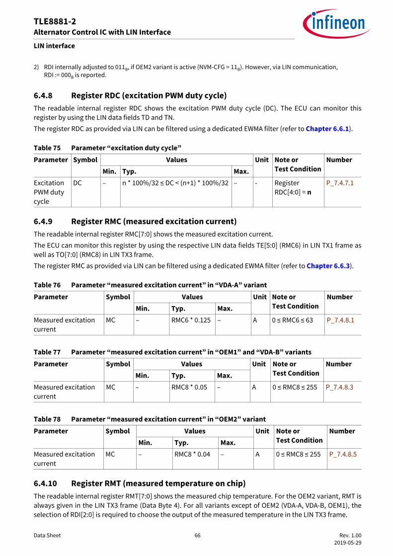
Data Sheet 66 Rev. 1.00 2019-05-29
TLE8881-2Alternator Control IC with LIN Interface
LIN interface
6.4.8 Register RDC (excitation PWM duty cycle)The readable internal register RDC shows the excitation PWM duty cycle (DC). The ECU can monitor thisregister by using the LIN data fields TD and TN.The register RDC as provided via LIN can be filtered using a dedicated EWMA filter (refer to Chapter 6.6.1).
6.4.9 Register RMC (measured excitation current)The readable internal register RMC[7:0] shows the measured excitation current.The ECU can monitor this register by using the respective LIN data fields TE[5:0] (RMC6) in LIN TX1 frame aswell as TO[7:0] (RMC8) in LIN TX3 frame.The register RMC as provided via LIN can be filtered using a dedicated EWMA filter (refer to Chapter 6.6.3).
6.4.10 Register RMT (measured temperature on chip)The readable internal register RMT[7:0] shows the measured chip temperature. For the OEM2 variant, RMT isalways given in the LIN TX3 frame (Data Byte 4). For all variants except of OEM2 (VDA-A, VDA-B, OEM1), theselection of RDI[2:0] is required to choose the output of the measured temperature in the LIN TX3 frame.
2) RDI internally adjusted to 011B, if OEM2 variant is active (NVM-CFG = 11B). However, via LIN communication, RDI := 000B is reported.
Table 75 Parameter “excitation duty cycle”Parameter Symbol Values Unit Note or
Test ConditionNumber
Min. Typ. Max.Excitation PWM duty cycle
DC – n * 100%/32 ≤ DC < (n+1) * 100%/32 – - Register RDC[4:0] = n
P_7.4.7.1
Table 76 Parameter “measured excitation current” in “VDA-A” variantParameter Symbol Values Unit Note or
Test ConditionNumber
Min. Typ. Max.Measured excitation current
MC – RMC6 * 0.125 – A 0 ≤ RMC6 ≤ 63 P_7.4.8.1
Table 77 Parameter “measured excitation current” in “OEM1” and “VDA-B” variantsParameter Symbol Values Unit Note or
Test ConditionNumber
Min. Typ. Max.Measured excitation current
MC – RMC8 * 0.05 – A 0 ≤ RMC8 ≤ 255 P_7.4.8.3
Table 78 Parameter “measured excitation current” in “OEM2” variantParameter Symbol Values Unit Note or
Test ConditionNumber
Min. Typ. Max.Measured excitation current
MC – RMC8 * 0.04 – A 0 ≤ RMC8 ≤ 255 P_7.4.8.5

Data Sheet 67 Rev. 1.00 2019-05-29
TLE8881-2Alternator Control IC with LIN Interface
LIN interface
The ECU can monitor this register by using the LIN data field TV of TX3.
6.4.11 Register RMV (measured voltage at VBA terminal)The readable internal register RMV[7:0] shows the measured voltage VBA. It is necessary to address RDI[2:0] toselect the output of the measured voltage in the LIN TX3 frame. This is only possible for the OEM1, VDA-A andVDA-B variants.The ECU can monitor this register by using the LIN data field TV of TX3. The measurable voltage is constrainedto the range of 8 V to 24 V.The register RMV as provided via LIN can be filtered using a dedicated EWMA filter (refer to Chapter 6.6.2).
Table 79 Parameter “measured temperature on chip” for OEM1, VDA-A and VDA-B variantsParameter Symbol Values Unit Note or
Test ConditionNumber
Min. Typ. Max.
Register measured temperature on chip
RMT 0 – 63 – All LIN frame variants P_7.4.9.1
Measured temperature MT – -42 + RMT * 4 ≤ TJ < -38 + RMT * 4
– °C 1)
1) The shown values for the measured temperature on chip do not include the temperature measurement tolerance.
P_7.4.9.2
Table 80 Parameter “measured temperature on chip” for OEM2 variantParameter Symbol Values Unit Note or
Test ConditionNumber
Min. Typ. Max.
Register measured temperature on chip
RMT 0 – 255 – All LIN frame variants P_7.4.9.3
Measured temperature MT – -42 + RMT ≤ TJ < -41 + RMT
– °C 1)
1) The shown values for the measured temperature on chip do not include the temperature measurement tolerance.
P_7.4.9.4
Table 81 Parameter “measured voltage at terminal VBA”Parameter Symbol Values Uni
tNote or Test Condition
NumberMin. Typ. Max.
Register “measured voltage at VBA terminal”
RMV 0 – 255 - All LIN frame variants
P_7.4.10.1
Measured voltage at VBA terminal
MV1)
1) The shown values for the voltage on terminal BA don’t include the voltage measurement tolerance.
Typ. value - 50 mV
8V+ RMV * 100 mV
Typ. value + 50 mV
mV 0 ≤ RMV < 161 P_7.4.10.2
Measured voltage at VBA terminal
MV 24 – – V 161 ≤ RMV < 255 P_7.4.10.3
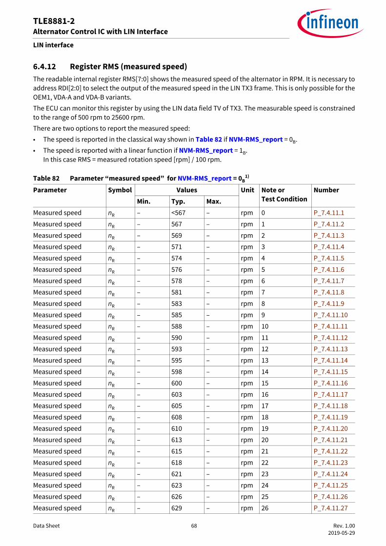
Data Sheet 68 Rev. 1.00 2019-05-29
TLE8881-2Alternator Control IC with LIN Interface
LIN interface
6.4.12 Register RMS (measured speed)The readable internal register RMS[7:0] shows the measured speed of the alternator in RPM. It is necessary toaddress RDI[2:0] to select the output of the measured speed in the LIN TX3 frame. This is only possible for theOEM1, VDA-A and VDA-B variants.The ECU can monitor this register by using the LIN data field TV of TX3. The measurable speed is constrainedto the range of 500 rpm to 25600 rpm.There are two options to report the measured speed:• The speed is reported in the classical way shown in Table 82 if NVM-RMS_report = 0B.• The speed is reported with a linear function if NVM-RMS_report = 1B.
In this case RMS = measured rotation speed [rpm] / 100 rpm.
Table 82 Parameter “measured speed” for NVM-RMS_report = 0B1)
Parameter Symbol Values Unit Note or Test Condition
NumberMin. Typ. Max.
Measured speed nR – <567 – rpm 0 P_7.4.11.1
Measured speed nR – 567 – rpm 1 P_7.4.11.2
Measured speed nR – 569 – rpm 2 P_7.4.11.3
Measured speed nR – 571 – rpm 3 P_7.4.11.4
Measured speed nR – 574 – rpm 4 P_7.4.11.5
Measured speed nR – 576 – rpm 5 P_7.4.11.6
Measured speed nR – 578 – rpm 6 P_7.4.11.7
Measured speed nR – 581 – rpm 7 P_7.4.11.8
Measured speed nR – 583 – rpm 8 P_7.4.11.9
Measured speed nR – 585 – rpm 9 P_7.4.11.10
Measured speed nR – 588 – rpm 10 P_7.4.11.11
Measured speed nR – 590 – rpm 11 P_7.4.11.12
Measured speed nR – 593 – rpm 12 P_7.4.11.13
Measured speed nR – 595 – rpm 13 P_7.4.11.14
Measured speed nR – 598 – rpm 14 P_7.4.11.15
Measured speed nR – 600 – rpm 15 P_7.4.11.16
Measured speed nR – 603 – rpm 16 P_7.4.11.17
Measured speed nR – 605 – rpm 17 P_7.4.11.18
Measured speed nR – 608 – rpm 18 P_7.4.11.19
Measured speed nR – 610 – rpm 19 P_7.4.11.20
Measured speed nR – 613 – rpm 20 P_7.4.11.21
Measured speed nR – 615 – rpm 21 P_7.4.11.22
Measured speed nR – 618 – rpm 22 P_7.4.11.23
Measured speed nR – 621 – rpm 23 P_7.4.11.24
Measured speed nR – 623 – rpm 24 P_7.4.11.25
Measured speed nR – 626 – rpm 25 P_7.4.11.26
Measured speed nR – 629 – rpm 26 P_7.4.11.27

Data Sheet 69 Rev. 1.00 2019-05-29
TLE8881-2Alternator Control IC with LIN Interface
LIN interface
Measured speed nR – 632 – rpm 27 P_7.4.11.28
Measured speed nR – 634 – rpm 28 P_7.4.11.29
Measured speed nR – 637 – rpm 29 P_7.4.11.30
Measured speed nR – 640 – rpm 30 P_7.4.11.31
Measured speed nR – 643 – rpm 31 P_7.4.11.32
Measured speed nR – 646 – rpm 32 P_7.4.11.33
Measured speed nR – 649 – rpm 33 P_7.4.11.34
Measured speed nR – 652 – rpm 34 P_7.4.11.35
Measured speed nR – 655 – rpm 35 P_7.4.11.36
Measured speed nR – 658 – rpm 36 P_7.4.11.37
Measured speed nR – 661 – rpm 37 P_7.4.11.38
Measured speed nR – 664 – rpm 38 P_7.4.11.39
Measured speed nR – 667 – rpm 39 P_7.4.11.40
Measured speed nR – 670 – rpm 40 P_7.4.11.41
Measured speed nR – 673 – rpm 41 P_7.4.11.42
Measured speed nR – 676 – rpm 42 P_7.4.11.43
Measured speed nR – 679 – rpm 43 P_7.4.11.44
Measured speed nR – 682 – rpm 44 P_7.4.11.45
Measured speed nR – 686 – rpm 45 P_7.4.11.46
Measured speed nR – 689 – rpm 46 P_7.4.11.47
Measured speed nR – 692 – rpm 47 P_7.4.11.48
Measured speed nR – 696 – rpm 48 P_7.4.11.49
Measured speed nR – 699 – rpm 49 P_7.4.11.50
Measured speed nR – 702 – rpm 50 P_7.4.11.51
Measured speed nR – 706 – rpm 51 P_7.4.11.52
Measured speed nR – 709 – rpm 52 P_7.4.11.53
Measured speed nR – 713 – rpm 53 P_7.4.11.54
Measured speed nR – 716 – rpm 54 P_7.4.11.55
Measured speed nR – 720 – rpm 55 P_7.4.11.56
Measured speed nR – 724 – rpm 56 P_7.4.11.57
Measured speed nR – 727 – rpm 57 P_7.4.11.58
Measured speed nR – 731 – rpm 58 P_7.4.11.59
Measured speed nR – 735 – rpm 59 P_7.4.11.60
Measured speed nR – 738 – rpm 60 P_7.4.11.61
Measured speed nR – 742 – rpm 61 P_7.4.11.62
Measured speed nR – 746 – rpm 62 P_7.4.11.63
Measured speed nR – 750 – rpm 63 P_7.4.11.64
Table 82 Parameter “measured speed” (cont’d) for NVM-RMS_report = 0B1)
Parameter Symbol Values Unit Note or Test Condition
NumberMin. Typ. Max.
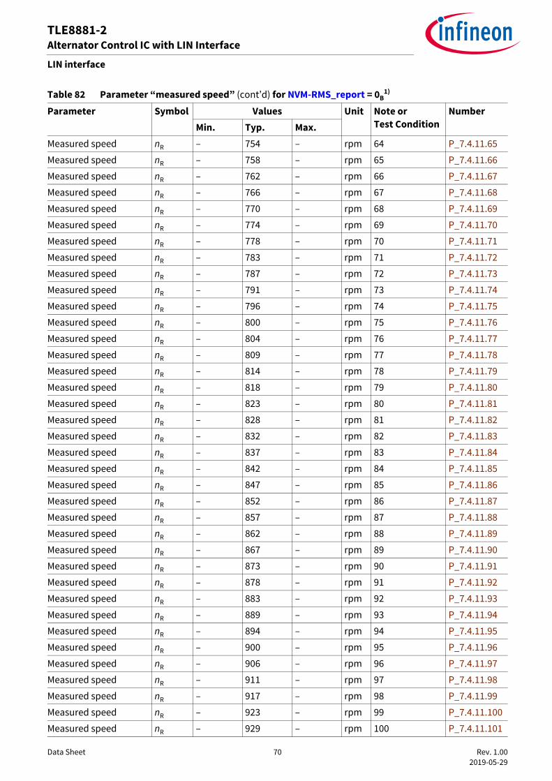
Data Sheet 70 Rev. 1.00 2019-05-29
TLE8881-2Alternator Control IC with LIN Interface
LIN interface
Measured speed nR – 754 – rpm 64 P_7.4.11.65
Measured speed nR – 758 – rpm 65 P_7.4.11.66
Measured speed nR – 762 – rpm 66 P_7.4.11.67
Measured speed nR – 766 – rpm 67 P_7.4.11.68
Measured speed nR – 770 – rpm 68 P_7.4.11.69
Measured speed nR – 774 – rpm 69 P_7.4.11.70
Measured speed nR – 778 – rpm 70 P_7.4.11.71
Measured speed nR – 783 – rpm 71 P_7.4.11.72
Measured speed nR – 787 – rpm 72 P_7.4.11.73
Measured speed nR – 791 – rpm 73 P_7.4.11.74
Measured speed nR – 796 – rpm 74 P_7.4.11.75
Measured speed nR – 800 – rpm 75 P_7.4.11.76
Measured speed nR – 804 – rpm 76 P_7.4.11.77
Measured speed nR – 809 – rpm 77 P_7.4.11.78
Measured speed nR – 814 – rpm 78 P_7.4.11.79
Measured speed nR – 818 – rpm 79 P_7.4.11.80
Measured speed nR – 823 – rpm 80 P_7.4.11.81
Measured speed nR – 828 – rpm 81 P_7.4.11.82
Measured speed nR – 832 – rpm 82 P_7.4.11.83
Measured speed nR – 837 – rpm 83 P_7.4.11.84
Measured speed nR – 842 – rpm 84 P_7.4.11.85
Measured speed nR – 847 – rpm 85 P_7.4.11.86
Measured speed nR – 852 – rpm 86 P_7.4.11.87
Measured speed nR – 857 – rpm 87 P_7.4.11.88
Measured speed nR – 862 – rpm 88 P_7.4.11.89
Measured speed nR – 867 – rpm 89 P_7.4.11.90
Measured speed nR – 873 – rpm 90 P_7.4.11.91
Measured speed nR – 878 – rpm 91 P_7.4.11.92
Measured speed nR – 883 – rpm 92 P_7.4.11.93
Measured speed nR – 889 – rpm 93 P_7.4.11.94
Measured speed nR – 894 – rpm 94 P_7.4.11.95
Measured speed nR – 900 – rpm 95 P_7.4.11.96
Measured speed nR – 906 – rpm 96 P_7.4.11.97
Measured speed nR – 911 – rpm 97 P_7.4.11.98
Measured speed nR – 917 – rpm 98 P_7.4.11.99
Measured speed nR – 923 – rpm 99 P_7.4.11.100
Measured speed nR – 929 – rpm 100 P_7.4.11.101
Table 82 Parameter “measured speed” (cont’d) for NVM-RMS_report = 0B1)
Parameter Symbol Values Unit Note or Test Condition
NumberMin. Typ. Max.
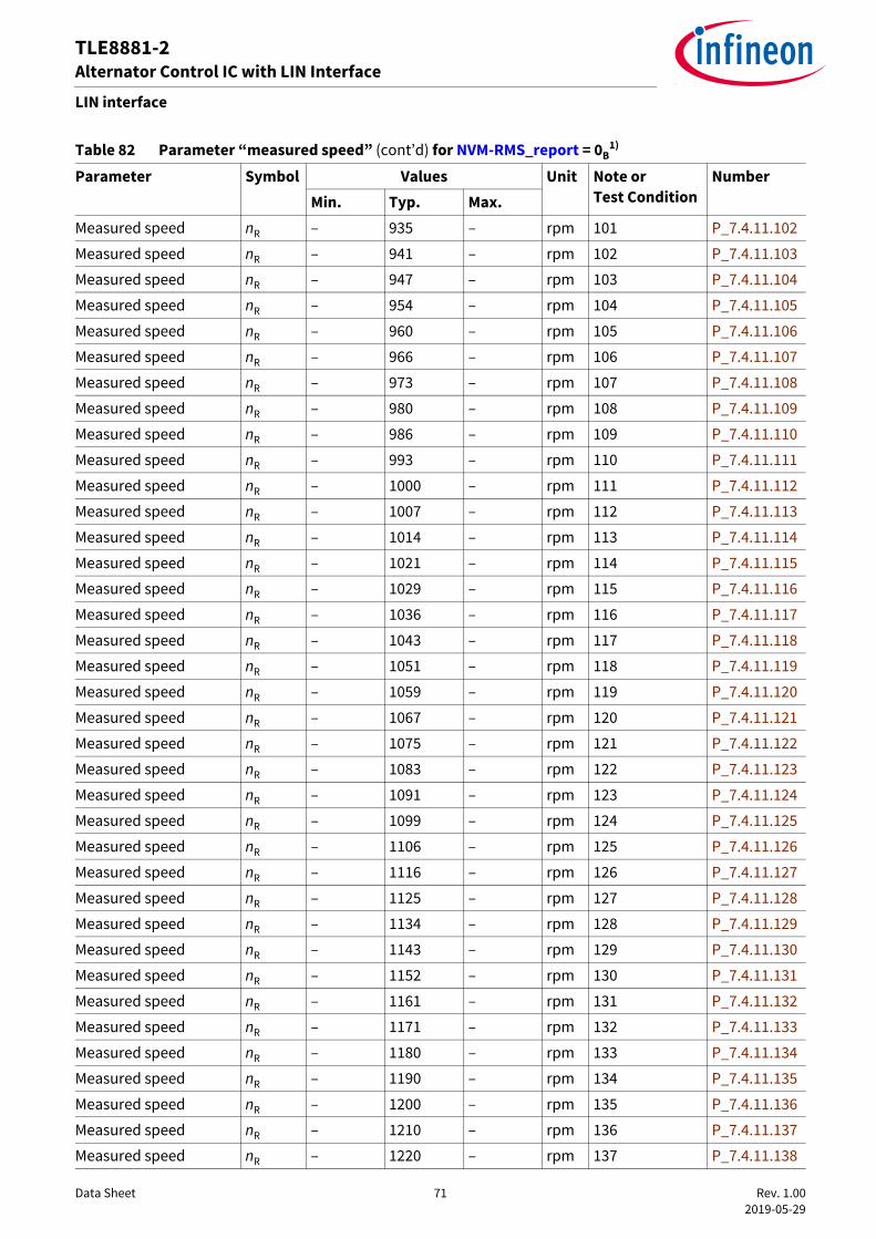
Data Sheet 71 Rev. 1.00 2019-05-29
TLE8881-2Alternator Control IC with LIN Interface
LIN interface
Measured speed nR – 935 – rpm 101 P_7.4.11.102
Measured speed nR – 941 – rpm 102 P_7.4.11.103
Measured speed nR – 947 – rpm 103 P_7.4.11.104
Measured speed nR – 954 – rpm 104 P_7.4.11.105
Measured speed nR – 960 – rpm 105 P_7.4.11.106
Measured speed nR – 966 – rpm 106 P_7.4.11.107
Measured speed nR – 973 – rpm 107 P_7.4.11.108
Measured speed nR – 980 – rpm 108 P_7.4.11.109
Measured speed nR – 986 – rpm 109 P_7.4.11.110
Measured speed nR – 993 – rpm 110 P_7.4.11.111
Measured speed nR – 1000 – rpm 111 P_7.4.11.112
Measured speed nR – 1007 – rpm 112 P_7.4.11.113
Measured speed nR – 1014 – rpm 113 P_7.4.11.114
Measured speed nR – 1021 – rpm 114 P_7.4.11.115
Measured speed nR – 1029 – rpm 115 P_7.4.11.116
Measured speed nR – 1036 – rpm 116 P_7.4.11.117
Measured speed nR – 1043 – rpm 117 P_7.4.11.118
Measured speed nR – 1051 – rpm 118 P_7.4.11.119
Measured speed nR – 1059 – rpm 119 P_7.4.11.120
Measured speed nR – 1067 – rpm 120 P_7.4.11.121
Measured speed nR – 1075 – rpm 121 P_7.4.11.122
Measured speed nR – 1083 – rpm 122 P_7.4.11.123
Measured speed nR – 1091 – rpm 123 P_7.4.11.124
Measured speed nR – 1099 – rpm 124 P_7.4.11.125
Measured speed nR – 1106 – rpm 125 P_7.4.11.126
Measured speed nR – 1116 – rpm 126 P_7.4.11.127
Measured speed nR – 1125 – rpm 127 P_7.4.11.128
Measured speed nR – 1134 – rpm 128 P_7.4.11.129
Measured speed nR – 1143 – rpm 129 P_7.4.11.130
Measured speed nR – 1152 – rpm 130 P_7.4.11.131
Measured speed nR – 1161 – rpm 131 P_7.4.11.132
Measured speed nR – 1171 – rpm 132 P_7.4.11.133
Measured speed nR – 1180 – rpm 133 P_7.4.11.134
Measured speed nR – 1190 – rpm 134 P_7.4.11.135
Measured speed nR – 1200 – rpm 135 P_7.4.11.136
Measured speed nR – 1210 – rpm 136 P_7.4.11.137
Measured speed nR – 1220 – rpm 137 P_7.4.11.138
Table 82 Parameter “measured speed” (cont’d) for NVM-RMS_report = 0B1)
Parameter Symbol Values Unit Note or Test Condition
NumberMin. Typ. Max.

Data Sheet 72 Rev. 1.00 2019-05-29
TLE8881-2Alternator Control IC with LIN Interface
LIN interface
Measured speed nR – 1231 – rpm 138 P_7.4.11.139
Measured speed nR – 1241 – rpm 139 P_7.4.11.140
Measured speed nR – 1252 – rpm 140 P_7.4.11.141
Measured speed nR – 1263 – rpm 141 P_7.4.11.142
Measured speed nR – 1274 – rpm 142 P_7.4.11.143
Measured speed nR – 1286 – rpm 143 P_7.4.11.144
Measured speed nR – 1297 – rpm 144 P_7.4.11.145
Measured speed nR – 1309 – rpm 145 P_7.4.11.146
Measured speed nR – 1321 – rpm 146 P_7.4.11.147
Measured speed nR – 1333 – rpm 147 P_7.4.11.148
Measured speed nR – 1346 – rpm 148 P_7.4.11.149
Measured speed nR – 1358 – rpm 149 P_7.4.11.150
Measured speed nR – 1371 – rpm 150 P_7.4.11.151
Measured speed nR – 1385 – rpm 151 P_7.4.11.152
Measured speed nR – 1398 – rpm 152 P_7.4.11.153
Measured speed nR – 1412 – rpm 153 P_7.4.11.154
Measured speed nR – 1426 – rpm 154 P_7.4.11.155
Measured speed nR – 1440 – rpm 155 P_7.4.11.156
Measured speed nR – 1455 – rpm 156 P_7.4.11.157
Measured speed nR – 1469 – rpm 157 P_7.4.11.158
Measured speed nR – 1485 – rpm 158 P_7.4.11.159
Measured speed nR – 1500 – rpm 159 P_7.4.11.160
Measured speed nR – 1516 – rpm 160 P_7.4.11.161
Measured speed nR – 1532 – rpm 161 P_7.4.11.162
Measured speed nR – 1548 – rpm 162 P_7.4.11.163
Measured speed nR – 1565 – rpm 163 P_7.4.11.164
Measured speed nR – 1582 – rpm 164 P_7.4.11.165
Measured speed nR – 1600 – rpm 165 P_7.4.11.166
Measured speed nR – 1618 – rpm 166 P_7.4.11.167
Measured speed nR – 1636 – rpm 167 P_7.4.11.168
Measured speed nR – 1655 – rpm 168 P_7.4.11.169
Measured speed nR – 1674 – rpm 169 P_7.4.11.170
Measured speed nR – 1694 – rpm 170 P_7.4.11.171
Measured speed nR – 1714 – rpm 171 P_7.4.11.172
Measured speed nR – 1735 – rpm 172 P_7.4.11.173
Measured speed nR – 1756 – rpm 173 P_7.4.11.174
Measured speed nR – 1778 – rpm 174 P_7.4.11.175
Table 82 Parameter “measured speed” (cont’d) for NVM-RMS_report = 0B1)
Parameter Symbol Values Unit Note or Test Condition
NumberMin. Typ. Max.

Data Sheet 73 Rev. 1.00 2019-05-29
TLE8881-2Alternator Control IC with LIN Interface
LIN interface
Measured speed nR – 1800 – rpm 175 P_7.4.11.176
Measured speed nR – 1823 – rpm 176 P_7.4.11.177
Measured speed nR – 1846 – rpm 177 P_7.4.11.178
Measured speed nR – 1870 – rpm 178 P_7.4.11.179
Measured speed nR – 1895 – rpm 179 P_7.4.11.180
Measured speed nR – 1920 – rpm 180 P_7.4.11.181
Measured speed nR – 1946 – rpm 181 P_7.4.11.182
Measured speed nR – 1973 – rpm 182 P_7.4.11.183
Measured speed nR – 2000 – rpm 183 P_7.4.11.184
Measured speed nR – 2028 – rpm 184 P_7.4.11.185
Measured speed nR – 2057 – rpm 185 P_7.4.11.186
Measured speed nR – 2087 – rpm 186 P_7.4.11.187
Measured speed nR – 2118 – rpm 187 P_7.4.11.188
Measured speed nR – 2149 – rpm 188 P_7.4.11.189
Measured speed nR – 2182 – rpm 189 P_7.4.11.190
Measured speed nR – 2215 – rpm 190 P_7.4.11.191
Measured speed nR – 2250 – rpm 191 P_7.4.11.192
Measured speed nR – 2286 – rpm 192 P_7.4.11.193
Measured speed nR – 2323 – rpm 193 P_7.4.11.194
Measured speed nR – 2361 – rpm 194 P_7.4.11.195
Measured speed nR – 2400 – rpm 195 P_7.4.11.196
Measured speed nR – 2441 – rpm 196 P_7.4.11.197
Measured speed nR – 2483 – rpm 197 P_7.4.11.198
Measured speed nR – 2526 – rpm 198 P_7.4.11.199
Measured speed nR – 2571 – rpm 199 P_7.4.11.200
Measured speed nR – 2618 – rpm 200 P_7.4.11.201
Measured speed nR – 2667 – rpm 201 P_7.4.11.202
Measured speed nR – 2717 – rpm 202 P_7.4.11.203
Measured speed nR – 2769 – rpm 203 P_7.4.11.204
Measured speed nR – 2824 – rpm 204 P_7.4.11.205
Measured speed nR – 2880 – rpm 205 P_7.4.11.206
Measured speed nR – 2939 – rpm 206 P_7.4.11.207
Measured speed nR – 3000 – rpm 207 P_7.4.11.208
Measured speed nR – 3064 – rpm 208 P_7.4.11.209
Measured speed nR – 3130 – rpm 209 P_7.4.11.210
Measured speed nR – 3200 – rpm 210 P_7.4.11.211
Measured speed nR – 3273 – rpm 211 P_7.4.11.212
Table 82 Parameter “measured speed” (cont’d) for NVM-RMS_report = 0B1)
Parameter Symbol Values Unit Note or Test Condition
NumberMin. Typ. Max.

Data Sheet 74 Rev. 1.00 2019-05-29
TLE8881-2Alternator Control IC with LIN Interface
LIN interface
Measured speed nR – 3349 – rpm 212 P_7.4.11.213
Measured speed nR – 3429 – rpm 213 P_7.4.11.214
Measured speed nR – 3512 – rpm 214 P_7.4.11.215
Measured speed nR – 3600 – rpm 215 P_7.4.11.216
Measured speed nR – 3692 – rpm 216 P_7.4.11.217
Measured speed nR – 3789 – rpm 217 P_7.4.11.218
Measured speed nR – 3892 – rpm 218 P_7.4.11.219
Measured speed nR – 4000 – rpm 219 P_7.4.11.220
Measured speed nR – 4114 – rpm 220 P_7.4.11.221
Measured speed nR – 4235 – rpm 221 P_7.4.11.222
Measured speed nR – 4364 – rpm 222 P_7.4.11.223
Measured speed nR – 4500 – rpm 223 P_7.4.11.224
Measured speed nR – 4645 – rpm 224 P_7.4.11.225
Measured speed nR – 4800 – rpm 225 P_7.4.11.226
Measured speed nR – 4966 – rpm 226 P_7.4.11.227
Measured speed nR – 5143 – rpm 227 P_7.4.11.228
Measured speed nR – 5333 – rpm 228 P_7.4.11.229
Measured speed nR – 5538 – rpm 229 P_7.4.11.230
Measured speed nR – 5760 – rpm 230 P_7.4.11.231
Measured speed nR – 6000 – rpm 231 P_7.4.11.232
Measured speed nR – 6261 – rpm 232 P_7.4.11.233
Measured speed nR – 6545 – rpm 233 P_7.4.11.234
Measured speed nR – 6857 – rpm 234 P_7.4.11.235
Measured speed nR – 7200 – rpm 235 P_7.4.11.236
Measured speed nR – 7579 – rpm 236 P_7.4.11.237
Measured speed nR – 8000 – rpm 237 P_7.4.11.238
Measured speed nR – 8471 – rpm 238 P_7.4.11.239
Measured speed nR – 9000 – rpm 239 P_7.4.11.240
Measured speed nR – 9600 – rpm 240 P_7.4.11.241
Measured speed nR – 10266 – rpm 241 P_7.4.11.242
Measured speed nR – 11077 – rpm 242 P_7.4.11.243
Measured speed nR – 12000 – rpm 243 P_7.4.11.244
Measured speed nR – 13091 – rpm 244 P_7.4.11.245
Measured speed nR – 14400 – rpm 245 P_7.4.11.246
Measured speed nR – 16000 – rpm 246 P_7.4.11.247
Measured speed nR – 18000 – rpm 247 P_7.4.11.248
Measured speed nR – 20571 – rpm 248 P_7.4.11.249
Table 82 Parameter “measured speed” (cont’d) for NVM-RMS_report = 0B1)
Parameter Symbol Values Unit Note or Test Condition
NumberMin. Typ. Max.

Data Sheet 75 Rev. 1.00 2019-05-29
TLE8881-2Alternator Control IC with LIN Interface
LIN interface
6.4.13 Register RSUPP and RCLASSThe readable internal register RSUPP[2:0] contains the alternator supplier code. The ECU can monitor thisregister by using the LIN data field TH.The readable internal register RCLASS[4:0] contains the alternator class code. The ECU can monitor thisregister by using the LIN data field TI.The registers RSUPP and RCLASS are loaded from the EEPROM.
6.5 Default register contentThe registers shown in table Table 84 are writable registers. Therefore, these registers will be set by the deviceif: • a logic reset occurs, or • the TLE8881-2 wakes up from stand-by, or • the state machine enters the state “default operation”.
Measured speed nR – – – rpm 249 P_7.4.11.250
Measured speed nR – – – rpm 250 P_7.4.11.251
Measured speed nR – – – rpm 251 P_7.4.11.252
Measured speed nR – – – rpm 252 P_7.4.11.253
Measured speed nR – – – rpm 253 P_7.4.11.254
Measured speed nR – – – rpm 254 P_7.4.11.255
Measured speed nR – – – rpm 255 P_7.4.11.2561) Speed values represent the threshold for switching to the coding shown in the table. The shown values do not include
the speed measurement tolerance.
Table 83 Parameter “measured speed” for NVM-RMS_report = 1B
Parameter Symbol Values Unit Note or Test Condition
NumberMin. Typ. Max.
Register “Measured speed”
RMS 6 - 255 – – P_7.4.12.1
Measured speed nR1)
1) The shown values for the measured speed do not include the speed measurement tolerance.– RMS*100 – rpm 6≤RMS≤255 P_7.4.12.3
Table 82 Parameter “measured speed” (cont’d) for NVM-RMS_report = 0B1)
Parameter Symbol Values Unit Note or Test Condition
NumberMin. Typ. Max.

Data Sheet 76 Rev. 1.00 2019-05-29
TLE8881-2Alternator Control IC with LIN Interface
LIN interface
The registers shown in Table 85 are readable registers. These register will be initialized if:• a logic reset occurs, or• the TLE8881-2 wakes up from stand-by state.
Table 84 Default writable register contentTLE8881-2 register Description ReferenceRVSET[7:0] Dependent on NVM-VSET.
Without NVM modification (default values): VSET = 14.3 VVDA-A/OEM2: RVSET[7:2] := 100010B (= 34)VDA-B/OEM1: RVSET[7:0] := 10001000B (= 136)
Register RVSET (voltage setpoint), Section 6.4.1
RLRCBZ Dependent on NVM-LRCBZ and NVM-LRCBZ_0_SEL.Without NVM modification (default values): LRCBZ = 3 %RLRCBZ := 0B
Registers LRC (load response control), Section 6.4.3
RLRCRT[3:0] Dependent on NVM-LRCRT and NVM-LRCRT_1s.Without NVM modification (default values): LRCRT = 5 sVDA-A: RLRCRT[3:0] := 0011B (= 3)VDA-B/OEM1/OEM2: RLRCRT[3:0] := 0110B (= 6)
Registers LRC (load response control), Section 6.4.3
RLRCDIS[3:0] Dependent on NVM-LRCDIS.Without NVM modification: nLRCDIS = 4000 rpmRLRCDIS[3:0] := 1000B
Registers LRC (load response control), Section 6.4.3
RCLIM[7:0] Excitation current limitation disabled:RCLIM[7:0] := 00000000B (= 0)
Register RCLIM (excitation current limitation), Section 6.4.4
RDI[2:0] Request data indicatorRDI[2:0] := 000B
Register RDI (response data indicator), Section 6.4.7
RHT[2:0] THT = 160°C RHT[2:0] := 000B (0°C temperature delta to THT)
Register RHT (adjustment of high temperature threshold), Section 6.4.6
RFPARA RFPARA = 0B Register RFPARA (F-Para function), Section 6.4.5
Table 85 Default readable register contentTLE8881-2 register
Description Reference
RDC[4:0] Excitation PWM duty cycle DC = 0%RDC[4:0] := 00000B
Register RDC (excitation PWM duty cycle), Section 6.4.8
RMC6[5:0] Measured excitation current MC = 0 ARMC6[5:0] := 000000B (= 0)
Register RMC (measured excitation current), Section 6.4.9
RMC8[7:0] Measured excitation current MC = 0 ARMC8[7:0] := 00000000B (= 0)
Register RMC (measured excitation current), Section 6.4.9
RMV[7:0] Measured voltage MV = 8 VRMV[7:0] := 00000000B (= 0)
Register RMV (measured voltage at VBA terminal), Section 6.4.11
Data Sheet 77 Rev. 1.00 2019-05-29
TLE8881-2Alternator Control IC with LIN Interface
LIN interface
6.6 Register output filtersThe TLE8881-2 includes Exponentially Weighted Moving Average (EWMA) filters of the first-order with its cut-off frequency fFILT at τ = 63%. These filters are used for the output of some internal registers which arecommunicated via LIN TX frames. The filtered values are not applied to the excitation output stage andexcitation DMOS.
6.6.1 Filter for excitation PWM duty cycle (RDC filter)The excitation PWM duty cycle calculated by the TLE8881-2 during the regulation activity is readable via LINat the register RDC of the TX1 and TX3 commands after the EWMA filtering (see Chapter 6.4.8). The filteredvalue is not applied to the excitation output stage.The activation of the filter and its characteristics are configurable via NVM-DC_EWMA_K and depend on NVM-CFG.If the PSB (Phase Signal Boost) function is active, leading to switching between 100% (on-time) and 0% (off-time) of the excitation PWM duty cycle, the input of the filter is regulated by the NVM-DC_EWMA_MODE.PSB is an internal function to maintain the phase signal and is not relevant for computation models insideECU. The duty cycle which is communicated via LIN TX frames is used as input for most computation models. With the NVM-DC_EWMA_MODE parameter, a different input value during an activated PSB function can beselected to blank out this internal maintenance.With the DC_EWMA_mode_DC0 parameter, the input value of the filter during activated PSB function can beforced to zero. This parameter has priority over any setting in NVM-DC_EWMA_MODE.
RMT[7:0] VDA-A/VDA-B/OEM1:Measured temperature MT = 24…28°CRMT[7:0] := 00010010B (= 18)OEM2:Measured temperature MT = 31°CRMT[7:0] := 01001001B (= 73)
Register RMT (measured temperature on chip), Section 6.4.10
RMS[7:0] RMS[7:0] := 00000000B (< 560 rpm) Register RMS (measured speed), Section 6.4.12
RCLASS[4:0] Without NVM modification: 11111B (= 31) Register RSUPP and RCLASS, Section 6.4.13RSUPP[2:0] Without NVM modification: 0000001B (= 1) Register RSUPP and RCLASS, Section 6.4.13Diagnosis flags F-HT := 0
F-EL := 0F-ROT := 0F-CEF := 0F-CTO depends on state machine (refer to Chapter 4.4)
-
Table 85 Default readable register content (cont’d)
TLE8881-2 register
Description Reference
Data Sheet 78 Rev. 1.00 2019-05-29
TLE8881-2Alternator Control IC with LIN Interface
LIN interface
6.6.2 Filter for voltage measurement (RMV Filter)The measured voltage at the VBA pin is readable via LIN at the register RMV after the EWMA filtering (seeChapter 6.4.11).The activation of the filter and its characteristics are configurable via the NVM field NVM-MV_EWMA_K.
Table 86 Parameter for “RDC filter” if NVM-CFG = 10B
All parameters are valid for: -40°C < TJ < 150°C; VBA = 14.5 V unless otherwise specified:
Parameter Symbol Values Unit Note or Test Condition
NumberMin. Typ. Max.
RDC filter deactivated fDCF – – – Hz 1); NVM-DC_EWMA_K = 00B
1) Not subject to production test
P_7.6.1.5
RDC filter time fDCF 0.5 1 1.5 Hz 1); NVM-DC_EWMA_K = 01B
P_7.6.1.1
RDC filter time fDCF 3 5 7 Hz 1); NVM-DC_EWMA_K = 10B
P_7.6.1.2
RDC filter time fDCF 7 10 13 Hz 1); NVM-DC_EWMA_K = 11B
P_7.6.1.3
Table 87 Parameter for “RDC filter” if NVM-CFG ≠ 10B
All parameters are valid for: -40°C < TJ < 150°C; VBA=14.5 V unless otherwise specified:
Parameter Symbol Values Unit Note or Test Condition
NumberMin. Typ. Max.
Duty cycle filter time tDCF -15% NVM-DC_EWMA_K
+15% ms 1)
1) Not subject to production test
P_7.6.1.4
Table 88 Parameter for “RMV filter” All parameters are valid for: -40°C < TJ < 150°C; unless otherwise specified:
Parameter Symbol Values Unit Note or Test Condition
NumberMin. Typ. Max.
RMV filter deactivated fMVF – – – Hz 1); NVM-MV_EWMA_K = 00B
1) Not subject to production test
P_7.6.2.4
RMV filter time fMVF 0.5 1 1.5 Hz 1); NVM-MV_EWMA_K = 01B
P_7.6.2.1
RMV filter time fMVF 3 5 7 Hz 1); NVM-MV_EWMA_K = 10B
P_7.6.2.2
RMV filter time fMVF 7 10 13 Hz 1); NVM-MV_EWMA_K = 11B
P_7.6.2.3

Data Sheet 79 Rev. 1.00 2019-05-29
TLE8881-2Alternator Control IC with LIN Interface
LIN interface
6.6.3 Excitation current filter (RMC filter)The measured current is readable via LIN at the register RMC after the EWMA filtering (see Chapter 6.4.9).The activation of the excitation current filter and its characteristics are configurable via the NVM field NVM-MC_EWMA_K.
Table 89 Parameter for “RMC filter”All parameters are valid for: -40°C < TJ < 150°C; VBA = 14.5 V unless otherwise specified:
Parameter Symbol Values Unit Note or Test Condition
NumberMin. Typ. Max.
RMC filter deactivated fMCF – – – Hz 1); NVM-MC_EWMA_K = 00B
1) Not subject to production test
P_7.6.3.1
RMC filter time fMCF 0.5 1 1.5 Hz 1); NVM-MC_EWMA_K= 01B
P_7.6.3.1
RMC filter time fMCF 3 5 7 Hz 1); NVM-MC_EWMA_K = 10B
P_7.6.3.2
RMC filter time fMCF 7 10 13 Hz 1); NVM-MC_EWMA_K = 11B
P_7.6.3.3

Data Sheet 80 Rev. 1.00 2019-05-29
TLE8881-2Alternator Control IC with LIN Interface
LIN interface
6.7 LIN 2.1 diagnostic framesDiagnostic frames are part of the LIN 2.1 data link layer specification only.The TLE8881-2 is defined as a Class-1 device in the LIN 2.1 network.By design, the TLE8881-2 supports two dedicated LIN 2.1 services:• Assign frame ID range (Chapter 6.7.3)• Read by identifier (Chapter 6.7.4)
6.7.1 Node configuration / identificationIf the frame identifier 3CH or 3DH is identified, the upcoming frames are going to carry configuration andidentification data. It has to be distinguished between the Master Request Frame (MRF) and the SlaveResponse Frame (SRF), whereas the respective frame are notified by:• Master Request Frame (MRF): 3CH
• Slave Response Frame (SRF): 3DH
The requests are executed by the slave device as soon as the MRF is received and found to be valid (i.e. no biterrors, checksum ok, etc).MRF and SRF may be interleaved with an unconditional frame, e.g. MRF → RX → SRF.As defined in the LIN specification MRF with NAD = 00H (where the following data is neglected) is interpretedas a go-to-sleep command, regardless of the frame’s data bytes.
6.7.2 NAD, supplier ID, function ID and variantIn order to enable the LIN 2.1 services, the device’s node address (NAD) and at least the wildcard values of thefunction ID and the supplier ID should be known. The NAD is used in the MRF and SRF frames to address oneparticular slave node in a cluster, or to indicate the source of a response. The supplier ID is assigned to onesupplier by the LIN Consortium. Distinguishing between the different application functions of distinct devicescan handled by the function ID. The wildcard values are defined in the LIN 2.1 Protocol Specification. Thespecific values for the TLE8881-2 are given in Table 90.
All values are hard-wired. The NAD is implemented as a metal option (8 bit) and can be changed via NVM-ALT.Wildcards (= broadcasts) are fully supported by the TLE8881-2.Beside these fixed supplier ID, function ID and variant, the TLE8881-2 offers the alternator’s supplier ID(3 bits), the alternator class ID (5 bits), the ASIC Manufacturer ID (001B for Infineon) and the ASIC ID (5 bits) inthe TX2 frame, as given in Chapter 6.4.13.It has to be considered that the LIN master is responsible for collision-avoidance (e.g. requests for SRF afterbroadcast MRF).
Table 90 Overview of LIN2.1 diagnostic frames identification codingsMessage Type Identification Wildcard / broadcast NADSupplier ID 0066H 7FFFH (Wildcard)
Function ID 7007H FFFFH (Wildcard)
Variant 00H -
Alternator 1 NAD (if NVM-ALT = 0B) 46H 7FH (Broadcast NAD)
Alternator 2 NAD (if NVM-ALT = 1B) 47H 7FH (Broadcast NAD)

Data Sheet 81 Rev. 1.00 2019-05-29
TLE8881-2Alternator Control IC with LIN Interface
LIN interface
Broadcast NADBroadcast NAD will be used to send one MRF Frame to multiple LIN slaves in parallel. A LIN frame containing abroadcast NAD is sent to all LIN 2.1 slave nodes in the LIN network. In case of multiple responses (e.g. collisionson the bus), the LIN slave will detect a bit-error, abort the transmission and set the F-CEF flag.NAD = 00H is used for go-to-sleep.
Support for diagnostic NAD (7EH)Diagnostic NAD is only used for functional addressing for the transport layer. The TLE8881-2 is defined as aClass-1 device. Class-1 devices do not need to support the transport layer diagnostics.Therefore, the TLE8881-2 does not support this feature.
6.7.3 Assign frame ID range (LIN 2.1 service)This supported service allows the LIN master to reconfigure the frame identifiers (also called PID in LIN 2.1specification) of the slave. In order to ensure a proper behavior after start-up, the PIDs are set to their defaultvalues. By sending the correct assign-frame-ID-range command, a LIN master could change the PIDs to newvalues. Attention has to be paid to the fact that the TLE8881-2 will not check the newly assigned PIDs forcorrectness. This function is implemented to be LIN 2.1 compliant.As the OEM might not want to use the assign frame ID function, it can be deactivated in EEPROM via NVM-AFIDen.An assign-frame-ID-range command comprises of a kind of header, containing the NAD of the addresseddevice, the protocol control information (PCI) and a service identifier (SID). These three bytes follow after theactual LIN header containing synch-break, synch-byte and PID. The respective bytes are given in Table 91.
The NAD, PCI and SID are then followed by 5 data bytes. The first byte indicates the starting index (e.g. first PIDto modify), and the following 4 bytes indicate the new PID values. Refer to Figure 20 for an overview picture.Valid values for PIDs are FFH for “don't care”, i.e. do not modify this frame’s PID, 00H for “unset” which triggerthe frame inactive, and any valid PID value between 00H and 3BH. For the TLE8881-2, the command couldchange the PIDs of the frames RX, TX1, TX2 and TX3 (in the respective order regarding the incrementing index).The MRF and SRF (frames 3CH and 3DH) are hard-wired, thus their PIDs cannot be changed. The request (ifcorrect) is processed immediately after the reception of the Master Request Frame (MRF) is complete.
Figure 20 Assign-frame-ID-range MRF layout (NAD = 46H/47H, PCI = 06H, SID = B7H)
After processing an assign-frame-ID-range command, the TLE8881-2 responds to a consecutive SRF only if thecommand is processed correctly. There is no error-response to this service.
Table 91 Assign frame ID range service codingsByte name Byte content
Master Request Frame (MRF) PCI 06H
SID B7H
Slave Response Frame (SRF) PCI 01H
RSID F7H
NAD PCI SID Index Data(Index)
Data (Index+1)
Data (Index+2)
Data (Index+3)LIN header
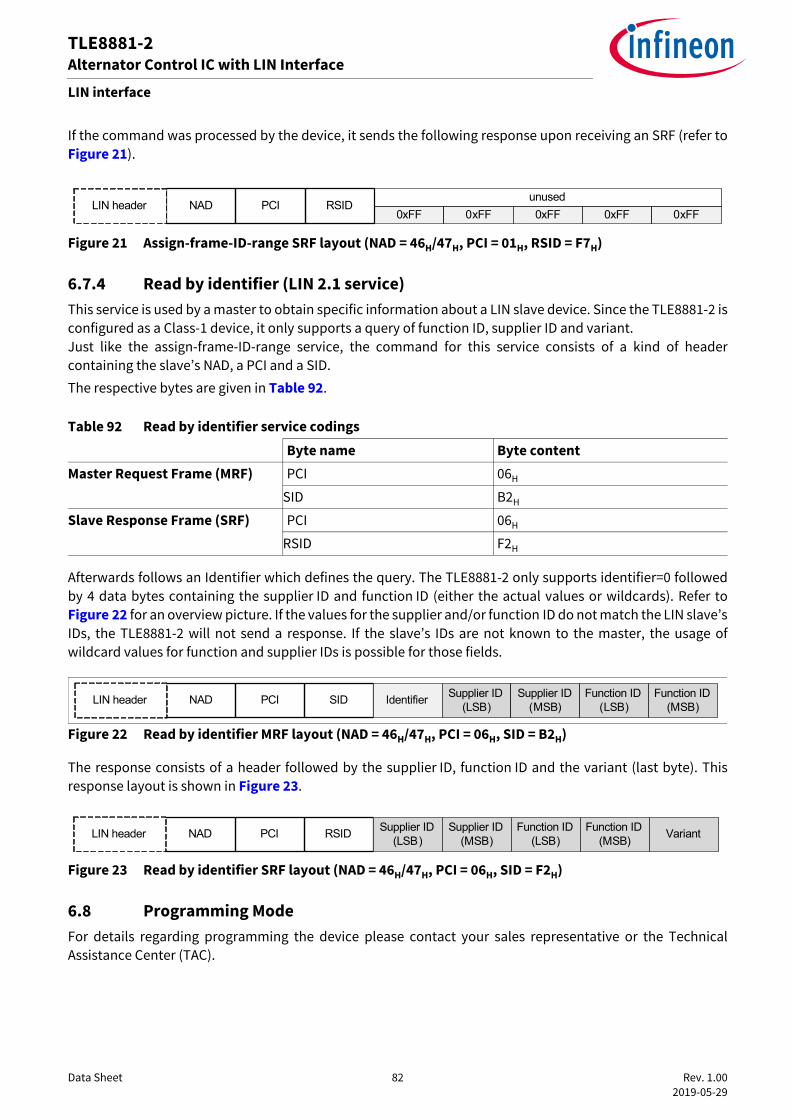
Data Sheet 82 Rev. 1.00 2019-05-29
TLE8881-2Alternator Control IC with LIN Interface
LIN interface
If the command was processed by the device, it sends the following response upon receiving an SRF (refer toFigure 21).
Figure 21 Assign-frame-ID-range SRF layout (NAD = 46H/47H, PCI = 01H, RSID = F7H)
6.7.4 Read by identifier (LIN 2.1 service)This service is used by a master to obtain specific information about a LIN slave device. Since the TLE8881-2 isconfigured as a Class-1 device, it only supports a query of function ID, supplier ID and variant. Just like the assign-frame-ID-range service, the command for this service consists of a kind of headercontaining the slave’s NAD, a PCI and a SID. The respective bytes are given in Table 92.
Afterwards follows an Identifier which defines the query. The TLE8881-2 only supports identifier=0 followedby 4 data bytes containing the supplier ID and function ID (either the actual values or wildcards). Refer toFigure 22 for an overview picture. If the values for the supplier and/or function ID do not match the LIN slave’sIDs, the TLE8881-2 will not send a response. If the slave’s IDs are not known to the master, the usage ofwildcard values for function and supplier IDs is possible for those fields.
Figure 22 Read by identifier MRF layout (NAD = 46H/47H, PCI = 06H, SID = B2H)
The response consists of a header followed by the supplier ID, function ID and the variant (last byte). Thisresponse layout is shown in Figure 23.
Figure 23 Read by identifier SRF layout (NAD = 46H/47H, PCI = 06H, SID = F2H)
6.8 Programming ModeFor details regarding programming the device please contact your sales representative or the TechnicalAssistance Center (TAC).
Table 92 Read by identifier service codingsByte name Byte content
Master Request Frame (MRF) PCI 06H
SID B2H
Slave Response Frame (SRF) PCI 06H
RSID F2H
NAD PCI0xFF 0xFF 0xFF 0xFF 0xFF
LIN headerunused
RSID
NAD PCI SID Identifier Supplier ID(LSB)
Supplier ID(MSB)
Function ID(LSB)
Function ID(MSB)LIN header
NAD PCI RSID Supplier ID(LSB)
Supplier ID(MSB)
Function ID(LSB)
Function ID(MSB)LIN header Variant

Data Sheet 83 Rev. 1.00 2019-05-29
TLE8881-2Alternator Control IC with LIN Interface
LIN interface
6.9 Internal LIN timersA set of internal timers is implemented in the core to support several functions for the LIN communication(refer to Table 93).All timings are directly dependant on the internal oscillator (Chapter 8.3).
Table 93 Parameters for internal LIN timersAll parameters are valid for: -40°C < TJ < 150°C; VBA = 14.5 V unless otherwise specified:
Parameter Symbol Values Unit Note or Test Condition
NumberMin. Typ. Max.
Delay time to reset diagnosis flag F-EL
tF-EL,Reset 20 62.5 100 ms 1)
1) Not subject to production test.
P_7.9.0.1
Test mode entry timer tTMSTART 130 145 160 ms 1); After wake-up or logic reset
P_7.9.0.8
Test mode deactivation timer
tTMOFF 9.1 10.3 11.5 s 1); After wake-up or logic reset
P_7.9.0.9
Table 94 Modified timers in test mode
Timer Parameter name Acceleration factortCTO No valid LIN communication timer 256
tF-EL Diagnosis flag debounce timer 32
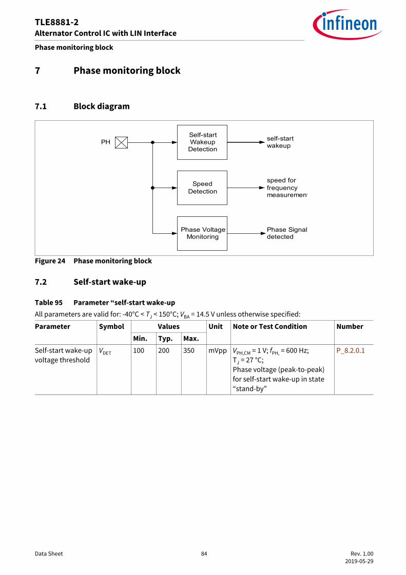
Data Sheet 84 Rev. 1.00 2019-05-29
TLE8881-2Alternator Control IC with LIN Interface
Phase monitoring block
7 Phase monitoring block
7.1 Block diagram
Figure 24 Phase monitoring block
7.2 Self-start wake-up
Table 95 Parameter “self-start wake-upAll parameters are valid for: -40°C < TJ < 150°C; VBA = 14.5 V unless otherwise specified:
Parameter Symbol Values Unit Note or Test Condition NumberMin. Typ. Max.
Self-start wake-up voltage threshold
VDET 100 200 350 mVpp VPH,CM = 1 V; fPH, = 600 Hz; TJ = 27 °C;Phase voltage (peak-to-peak) for self-start wake-up in state “stand-by”
P_8.2.0.1
Self-startWakeup
DetectionPH self-start
wakeup
Phase VoltageMonitoring
SpeedDetection
speed forfrequencymeasurement
Phase Signaldetected

Data Sheet 85 Rev. 1.00 2019-05-29
TLE8881-2Alternator Control IC with LIN Interface
Phase monitoring block
7.3 Speed detection
7.4 Phase monitoringThe phase voltage monitoring block monitors the voltage at the phase input PH. The voltage is used for thephase signal boost function (Chapter 5.11) and for the engine stop detection.
Table 96 Parameter “speed detection”All parameters are valid for: -40°C < TJ < 150°C; VBA = 14.5 V unless otherwise specified:
Parameter Symbol Values Unit Note or Test Condition NumberMin. Typ. Max.
Peak-to-peak speed detection threshold
VDET – 200 – mVpp Phase voltage (peak-to-peak) for speed detection in states “ComActive” and “default operation”
P_8.3.0.1
Peak-to-peak speed detection threshold
VDET – 800 – mVpp Phase voltage (peak-to-peak) for speed detection in state “pre-excitation” and CTO = 0 (no LIN communication time-out)
P_8.3.0.2
Peak-to-peak speed detection threshold
VDET – 800 – mVpp Phase voltage (peak-to-peak) for speed detection in state “normal operation”.
P_8.3.0.3
Table 97 Parameter phase monitoringAll parameters are valid for: -40°C < TJ < 150°C; VBA = 14.5 V unless otherwise specified:
Parameter Symbol Values Unit Note or Test Condition
NumberMin. Typ. Max.
Pull down resistor at terminal PH
RPHRD 20 33 50 kΩ In state “pre-excitation”
P_8.4.0.1
Pull down resistor at terminal PH
RPHRD 60 100 165 kΩ All states except “pre-excitation”
P_8.4.0.2
Phase Signal time-out tPH,TO 15 60 120 ms 1);2);1) Not subject to production test.2) In case of phase signal loss, an event is generated after a time-out tPH,TO. This event is used by the state machine to
ensure that in case of no valid LIN communication and too low rotor speed, the TLE8881-2 goes to stand-by mode.
P_8.4.0.3

Data Sheet 86 Rev. 1.00 2019-05-29
TLE8881-2Alternator Control IC with LIN Interface
Core functions
8 Core functions
8.1 Voltage referenceA band gap reference is used for internal comparisons to achieve calibrated results.
8.2 Internal supply referenceThe TLE8881-2 is equipped with the following voltage sources:• internal 5 V supply for analogue circuitry• internal 3.3 V supply for the CMOS logic circuitry
8.3 OscillatorThe oscillator generates the clock signal required by the logic functions (main control, regulation block,TLE8881-2 registers and LIN protocol handler).
8.4 Charge pumpThe charge pump is required for the excitation high-side driver. The charge pump does not require anyexternal energy storage capacitor.
Table 98 Parameter oscillatorAll parameters are valid for: -40°C < TJ < 150°C; VBA = 14.5 V unless otherwise specified:
Parameter Symbol Values Unit Note or Test Condition
NumberMin. Typ. Max.
Oscillator frequency fOSC 1.62 1.8 1.98 MHz Value is trimmed at 25°C
P_9.3.0.1

Data Sheet 87 Rev. 1.00 2019-05-29
TLE8881-2Alternator Control IC with LIN Interface
Core functions
8.5 Restore state functionDuring the operation of the TLE8881-2, a supply micro-cut can occur. The restore state function asimplemented restores the operation state as well as essential register values to avoid a perceptible disruptionin operation.
8.5.1 Supply micro-cut
Figure 25 Supply micro-cut
Table 99 Parameter micro-cutAll parameters are valid for: -40°C < TJ < 150°C; VBA = 14.5 V unless otherwise specified:
Parameter Symbol Values Unit Note or Test Condition
NumberMin. Typ. Max.
Supply micro-cut repetition period
TMC1 10 – – ms 1); VBA > 0 V
1) Not subject to production test.
P_9.5.1.1
Supply micro-cut duration
TMC2 – – 100 μs 1); VBA > 0 V P_9.5.1.2
Supply micro-cut fall time
TMC3 5 – 50 μs 1); VBA > 0 V P_9.5.1.3
Supply micro-cut rise time
TMC4 5 – 50 μs 1); VBA > 0 V P_9.5.1.4
90%
10%
TMC2
TMC1
TMC3 TMC4
VBA
time

Data Sheet 88 Rev. 1.00 2019-05-29
TLE8881-2Alternator Control IC with LIN Interface
Core functions
8.5.2 Restore state eventIf a logic inadvertent reset occurs in the state normal operation or default operation, the following informationis stored for at least (TMC2+TMC3+TMC4) and restored after reset:• Normal operation data bit (fast startup in normal operation or default operation)• Regulation voltage setpoint (VSET) with a resolution of 100 mV• LRC rise time (LRCRT)• Targeted FEXLIM region• F-Para function activation (as requested via the LIN RX frame)After the reset the following actions are executed if a valid restore state condition is detected:• The stored register information is restored, all other registers are initialized (like after wake-up).• The LRC duty cycle is set to 100%.• Dependent on the stored information, the state machine continues either on the state “normal operation”
or “default operation”.The restore state function does not store information related to the assign frame ID range service (refer toChapter 6.7.3). This means that any previously assigned LIN IDs have to be re-assigned after inadvertentreset.
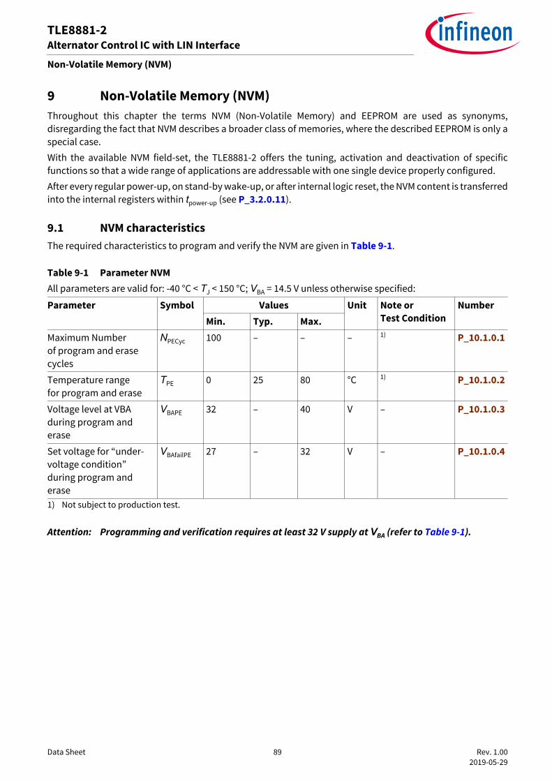
Data Sheet 89 Rev. 1.00 2019-05-29
TLE8881-2Alternator Control IC with LIN Interface
Non-Volatile Memory (NVM)
9 Non-Volatile Memory (NVM)Throughout this chapter the terms NVM (Non-Volatile Memory) and EEPROM are used as synonyms,disregarding the fact that NVM describes a broader class of memories, where the described EEPROM is only aspecial case.With the available NVM field-set, the TLE8881-2 offers the tuning, activation and deactivation of specificfunctions so that a wide range of applications are addressable with one single device properly configured.After every regular power-up, on stand-by wake-up, or after internal logic reset, the NVM content is transferredinto the internal registers within tpower-up (see P_3.2.0.11).
9.1 NVM characteristicsThe required characteristics to program and verify the NVM are given in Table 9-1.
Attention: Programming and verification requires at least 32 V supply at VBA (refer to Table 9-1).
Table 9-1 Parameter NVMAll parameters are valid for: -40 °C < TJ < 150 °C; VBA = 14.5 V unless otherwise specified:
Parameter Symbol Values Unit Note or Test Condition
NumberMin. Typ. Max.
Maximum Number of program and erase cycles
NPECyc 100 – – – 1)
1) Not subject to production test.
P_10.1.0.1
Temperature range for program and erase
TPE 0 25 80 °C 1) P_10.1.0.2
Voltage level at VBA during program and erase
VBAPE 32 – 40 V – P_10.1.0.3
Set voltage for “under-voltage condition” during program and erase
VBAfailPE 27 – 32 V – P_10.1.0.4

Data Sheet 90 Rev. 1.00 2019-05-29
TLE8881-2Alternator Control IC with LIN Interface
Non-Volatile Memory (NVM)
9.2 NVM register descriptionThe register descriptions of the NVM - which can be accessed via the programming mode - are presented anddescribed in this chapter.
9.2.1 List overviewTable 9-2 to Table 9-5 show a listed overview of all accessible NVM fields.

Data Sheet 91 Rev. 1.00 2019-05-29
TLE8881-2Alternator Control IC with LIN Interface
Non-Volatile Memory (NVM)
Table 9-2 List overview of accessible NVM fields (sorted by placement in the EEPROM)Address Section Field Short name00H 0 NVM-LINRX LIN RX frame ID
00H 0 NVM-ALT Alternator number in vehicle LIN network
00H 0 NVM-LIN LIN version
00H 1 NVM-LINTX1 LIN TX1 frame ID
00H 1 NVM-RPARA_SEL Selection of parameter set for F-PARA
00H 2 NVM-CFG OEM configuration
01H 0 NVM-LINTX2 LIN TX2 frame ID
01H 0 NVM-LRCBZ_0_SEL LRC blind zone “0” selection
Table 9-3 List overview of accessible NVM fields (NVM-LIN=0B)Address Section Field Short name01H 1 NVM-LINTX3 LINTX3 frame ID
01H 1 NVM-LEOLRC LRC after LEO function
01H 1 NVM-AFIDen “Assign frame ID” service disable
Table 9-4 List overview of accessible NVM fields (NVM-LIN=1B)Address Section Field Short name01H 1 NVM-LINTX3 LINTX3 frame ID
01H 1 NVM-LEOLRC LRC after LEO function
01H 1 NVM-3Ddis Enable/disable 3D frame for LIN1.3
Table 9-5 List overview of accessible NVM fields (sorted by placement in the EEPROM)Address Section Field Short name01H 2 NVM-EOFF Activation of excitation-off state
02H 0 NVM-SUPP Alternator supplier
02H 0 NVM-CLASS Alternator class
02H 1 NVM-DC_EWMA_MODE Excitation duty cycle filter mode during Phase Signal Boost (PSB)
02H 1 NVM-DC_EWMA_K Excitation duty cycle filter coefficients
02H 1 NVM-RMS_report RMS reporting
02H 1 NVM-MC_EWMA_K Excitation current filter coefficients
02H 1 NVM-MV_EWMA_K Measurement voltage filter coefficients
02H 2 NVM-PP Alternator pole pairs
03H 0 NVM-HEO_ANdis Disable analogue HEO function
03H 0 NVM-LRCRT LRC rise-time for default operation
03H 0 NVM-LEOTIMERdis LEO (Low-Voltage Excitation On) function disable switch
03H 1 NVM-VSET_report Type of VSET reporting selection

Data Sheet 92 Rev. 1.00 2019-05-29
TLE8881-2Alternator Control IC with LIN Interface
Non-Volatile Memory (NVM)
03H 1 NVM-PREEXC_27HZ5_DIS Pre-excitation duty cycle selection
03H 1 NVM-PEXCDC Duty cycle in pre-excitation state
03H 1 NVM-LRCBZ Selection of the LRC blind zone in default operation state
03H 2 NVM-SSS Self-start speed threshold
04H 0 NVM-LEO Default VLOW for LEO function (Low Voltage Excitation ON)
04H 0 NVM-LEO_ERR_EN LEO/F-EL interaction setting
04H 0 NVM-T_EL_ERR Debounce time of electrical error flag (F-EL)
04H 0 NVM-HEO_ERR_EN Overvoltage error flag switch
04H 0 NVM-FROT_SEL Configuration for the mechanical error flag F-ROT
04H 1 NVM-THT Absolute threshold for high-temperature voltage compensation
04H 1 NVM-HTG Gradient for high-temperature voltage compensation
04H 1 NVM-CLIM Excitation overcurrent protection threshold
04H 2 NVM-T_PSB_ON_MAX Maximum ON-time for PSB (Phase Signal Boost) function
05H 0 NVM-FEXLIM_PCLIM1 Frequency dependent current limitation (FEXLIM) feature: PCLIM1 region
05H 0 NVM-FEXLIM_EN Enable/disable frequency dependent current limitation (FEXLIM) function
05H 0 NVM-FEXLIM_PCLIM2 Frequency dependent current limitation (FEXLIM) feature: PCLIM2 region
05H 1 Reserved Reserved
05H 2 Reserved Reserved
06H 0 NVM-LRCRT_1s Enable 1s option for the default LRC rise time
06H 0 NVM-VSET Voltage set-point for default operation
06H 0 DC_EWMA_mode_DC0 Excitation duty cycle filter mode during Phase Signal Boost (PSB)
06H 1 NVM-CSHT Disable curve shaping at high temperature
06H 1 NVM-LRCFT LRC fall-time
06H 1 NVM-IEXC100 Minimum excitation current at 100% DC to avoid open load detection
06H 2 Reserved Reserved
07H 0 NVM-Speed_TH Speed-dependent KiKp parameter sets (KiKp function) Speed threshold - upper value of hysteresis
07H 0 NVM-LRCDIS Rotor speed to disable LRC for default operation
07H 1 NVM-VoKiKp Voltage dependent KiKp function (VoKiKp function) configuration Enabling and VoKiKp up threshold
07H 1 NVM-VoKiKp_low_HEO_speed
Voltage dependent KiKp function (VoKiKp) speed dependency
07H 1 NVM-KiKp KiKp function configuration
Table 9-5 List overview of accessible NVM fields (sorted by placement in the EEPROM) (cont’d)Address Section Field Short name

Data Sheet 93 Rev. 1.00 2019-05-29
TLE8881-2Alternator Control IC with LIN Interface
Non-Volatile Memory (NVM)
07H 1 NVM-LOW_HEO Speed-dependent lowering of the HEO limit (LowHEO function) Enabling and LowHEO voltage selection
07H 2 NVM-LOCK_EN Enable NVM Lock
Table 9-5 List overview of accessible NVM fields (sorted by placement in the EEPROM) (cont’d)Address Section Field Short name

Data Sheet 94 Rev. 1.00 2019-05-29
TLE8881-2Alternator Control IC with LIN Interface
Non-Volatile Memory (NVM)
9.2.2 Detailed description
NVM_A00_S0Address 00H - Section 0 (00H)Reset Value: 00H
7 6 5 4 3 2 1 0
NVM-LIN NVM-ALT NVM-LINRX
rw rw rw
Field Bits Type DescriptionNVM-LINRX 5:0 rw LIN RX frame ID
Default LIN RX frame ID (refer to Chapter 6.3.2).
NVM-ALT 6 rw Alternator number in vehicle LIN networkDefines the alternator number in the vehicle LIN network. This switchin independent from configuration of the LIN IDs, but relates to the LIN2.1 NAD (refer to Chapter 6.7.2).0B Device is configured to be regulator #1 in implemented LIN
network (NAD=46H), 1B Device is configured to be regulator #2 in implemented LIN
network (NAD=47H),
NVM-LIN 7 rw LIN versionSelection of the compliance for the LIN communication standardspecification. This selection includes the usage of the classic orenhanced checksum and the related protocol features. (refer to Chapter 6.3.1)0B LIN 2.1, 1B LIN 1.3,

Data Sheet 95 Rev. 1.00 2019-05-29
TLE8881-2Alternator Control IC with LIN Interface
Non-Volatile Memory (NVM)
NVM_A00_S1Address 00H - Section 1 (00H)Reset Value: 00H
7 6 5 4 3 2 1 0
NVM-RPARA_SEL NVM-LINTX1
rw rw
Field Bits Type DescriptionNVM-LINTX1 5:0 rw LIN TX1 frame ID
Defines the LIN Identifier bits for the LIN TX1 frame. The relating paritybits are calculated internally (refer to Chapter 6.3.2).
NVM-RPARA_SEL
7:6 rw Selection of parameter set for F-PARAThe F-Para function can be activated by sending respective code “1” in LIN RX frame. If the F-Para function is active, a parameter setwith changed regulation dynamic is used (refer to Chapter 5.14).00B Slowest dynamic, 01B Slower dynamic, 10B Slow dynamic, 11B Normal dynamic,
NVM_A00_S2Address 00H - Section 2 (00H)Reset Value: 00H
7 6 5 4 3 2 1 0
Reserved NVM-CFG
r rw
Field Bits Type DescriptionNVM-CFG 1:0 rw OEM configuration
Dedicated LIN frame layouts for the LIN RX/TX3/TX4 frame and internal registers (e.g. default rise-time for the LRC function) can be adjusted by using this switch (refer to Chapter 6.3.1).00B VDA-A, 01B VDA-B, 10B OEM1, 11B OEM2,
Reserved 7:2 r ReservedReserved read-only area.
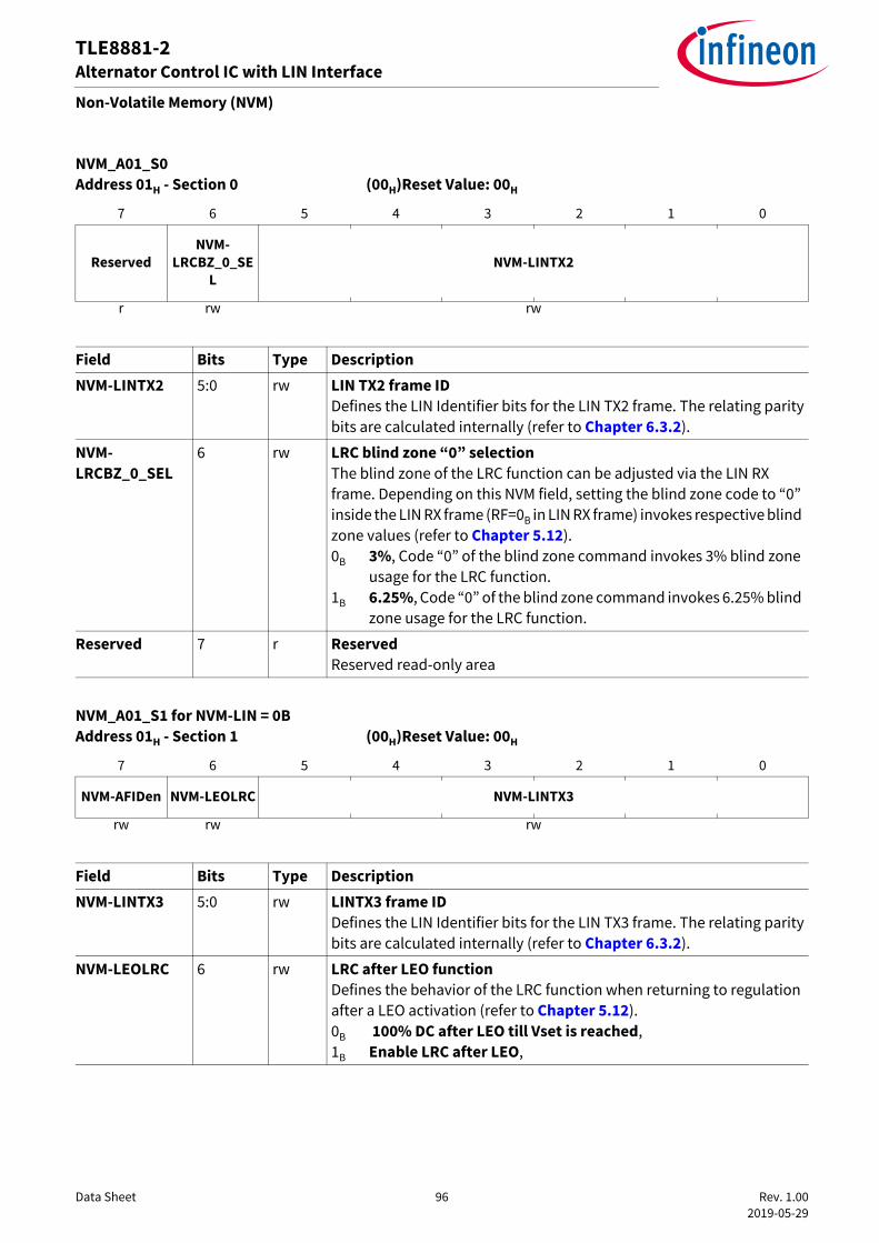
Data Sheet 96 Rev. 1.00 2019-05-29
TLE8881-2Alternator Control IC with LIN Interface
Non-Volatile Memory (NVM)
NVM_A01_S0Address 01H - Section 0 (00H)Reset Value: 00H
7 6 5 4 3 2 1 0
ReservedNVM-
LRCBZ_0_SEL
NVM-LINTX2
r rw rw
Field Bits Type DescriptionNVM-LINTX2 5:0 rw LIN TX2 frame ID
Defines the LIN Identifier bits for the LIN TX2 frame. The relating paritybits are calculated internally (refer to Chapter 6.3.2).
NVM-LRCBZ_0_SEL
6 rw LRC blind zone “0” selectionThe blind zone of the LRC function can be adjusted via the LIN RX frame. Depending on this NVM field, setting the blind zone code to “0” inside the LIN RX frame (RF=0B in LIN RX frame) invokes respective blind zone values (refer to Chapter 5.12).0B 3%, Code “0” of the blind zone command invokes 3% blind zone
usage for the LRC function.1B 6.25%, Code “0” of the blind zone command invokes 6.25% blind
zone usage for the LRC function.
Reserved 7 r ReservedReserved read-only area
NVM_A01_S1 for NVM-LIN = 0BAddress 01H - Section 1 (00H)Reset Value: 00H
7 6 5 4 3 2 1 0
NVM-AFIDen NVM-LEOLRC NVM-LINTX3
rw rw rw
Field Bits Type DescriptionNVM-LINTX3 5:0 rw LINTX3 frame ID
Defines the LIN Identifier bits for the LIN TX3 frame. The relating paritybits are calculated internally (refer to Chapter 6.3.2).
NVM-LEOLRC 6 rw LRC after LEO functionDefines the behavior of the LRC function when returning to regulation after a LEO activation (refer to Chapter 5.12).0B 100% DC after LEO till Vset is reached, 1B Enable LRC after LEO,

Data Sheet 97 Rev. 1.00 2019-05-29
TLE8881-2Alternator Control IC with LIN Interface
Non-Volatile Memory (NVM)
NVM-AFIDen 7 rw “Assign frame ID” service disable“Assign frame ID” service is a dedicated LIN 2.1 service to re-assignidentifier for a LIN frame (refer to Chapter 6.7.3).
Note: It is not recommended to use this service inside the real application, since micro-cuts of the voltage supply would lead to complete reset of the device including the reassign frame identifier.
0B Assign frame ID disabled , for LIN 2.1 (recommended for higher robustness)
1B Assign frame ID enabled, for LIN 2.1
NVM_A01_S1 for NVM-LIN = 1BAddress 01H - Section 1 (00H)Reset Value: 00H
7 6 5 4 3 2 1 0
NVM-3Ddis NVM-LEOLRC NVM-LINTX3
rw rw rw
Field Bits Type DescriptionNVM-LINTX3 5:0 rw LINTX3 frame ID
Defines the LIN Identifier bits for the LIN TX3 frame. The relating paritybits are calculated internally (refer to Chapter 6.3.2).
NVM-LEOLRC 6 rw LRC after LEO functionDefines the behavior of the LRC function when returning to regulation after a LEO activation (refer to Chapter 5.12).0B 100% DC after LEO till Vset is reached, 1B Enable LRC after LEO,
NVM-3Ddis 7 rw Enable/disable 3D frame for LIN1.3“3D disable” service is a dedicated LIN 1.3 service and used to enable/disable the 3D special LIN frame (refer to Chapter 6.3.2).0B 3D frame enabled, for LIN 1.31B 3D frame disabled, for LIN 1.3
NVM_A01_S2Address 01H - Section 2 (00H)Reset Value: 00H
7 6 5 4 3 2 1 0
Reserved NVM-EOFF
r rw
Field Bits Type Description
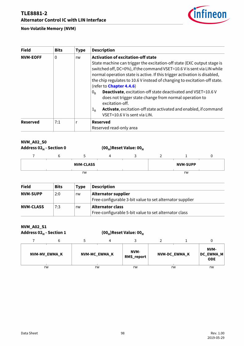
Data Sheet 98 Rev. 1.00 2019-05-29
TLE8881-2Alternator Control IC with LIN Interface
Non-Volatile Memory (NVM)
Field Bits Type DescriptionNVM-EOFF 0 rw Activation of excitation-off state
State machine can trigger the excitation-off state (EXC output stage is switched off, DC=0%), if the command VSET=10.6 V is sent via LIN while normal operation state is active. If this trigger activation is disabled, the chip regulates to 10.6 V instead of changing to excitation-off state. (refer to Chapter 4.4.6)0B Deactivate, excitation-off state deactivated and VSET=10.6 V
does not trigger state change from normal operation to excitation-off.
1B Activate, excitation-off state activated and enabled, if command VSET=10.6 V is sent via LIN.
Reserved 7:1 r ReservedReserved read-only area
NVM_A02_S0Address 02H - Section 0 (00H)Reset Value: 00H
7 6 5 4 3 2 1 0
NVM-CLASS NVM-SUPP
rw rw
Field Bits Type DescriptionNVM-SUPP 2:0 rw Alternator supplier
Free-configurable 3-bit value to set alternator supplier
NVM-CLASS 7:3 rw Alternator classFree-configurable 5-bit value to set alternator class
NVM_A02_S1Address 02H - Section 1 (00H)Reset Value: 00H
7 6 5 4 3 2 1 0
NVM-MV_EWMA_K NVM-MC_EWMA_K NVM-RMS_report NVM-DC_EWMA_K
NVM-DC_EWMA_M
ODE
rw rw rw rw rw

Data Sheet 99 Rev. 1.00 2019-05-29
TLE8881-2Alternator Control IC with LIN Interface
Non-Volatile Memory (NVM)
Field Bits Type DescriptionNVM-DC_EWMA_MODE
0 rw Excitation duty cycle filter mode during Phase Signal Boost (PSB)PSB is an internal function to maintain the phase signal and is not relevant for computation models inside ECU. DC is used as model input for most computations models, which is communicated via LIN TX frames. If the phase signal falls below the PSB threshold (e.g. due to voltage set-point below battery voltage level), the PSB function is activated until phase signal has been backed up again. The EWMA mode can be used to blank out this internal maintenance by using a different input value during an activated PSB function (refer to Chapter 6.6.1).The option Input := 0 can be selected by DC_EWMA_mode_DC0.0B Filter Input := DC from regulation, the EWMA filter will be fed
with DC from calculations coming out of the PI regulation (e.g. 0% DC, if VSET < VBA ).
1B Filter Input := DC from pre-excitation, the EWMA filter will be fed with a fixed DC as controlled by NVM-PEXCDC.
NVM-DC_EWMA_K
2:1 rw Excitation duty cycle filter coefficientsEnable/disable and cut-off frequency of the EWMA filter of the PWMduty cycle (refer to Chapter 6.6.1).00B None, (EWMA filter disabled)01B 1 Hz, if NVM-CFG is “OEM1”10B 5 Hz, if NVM-CFG is “OEM1”11B 10 Hz, if NVM-CFG is “OEM1”00B 35 ms, if NVM-CFG is not “OEM1”01B 70 ms, if NVM-CFG is not “OEM1”10B 140 ms, if NVM-CFG is not “OEM1”11B 210 ms, if NVM-CFG is not “OEM1”
NVM-RMS_report
3 rw RMS reportingSelection of the RMS reporting style (refer to Chapter 6.4.12).0B Classic reporting style, 1B Linear RMS reporting,
NVM-MC_EWMA_K
5:4 rw Excitation current filter coefficientsEnable/disable and cut-off frequency of the EWMA filter of the excitation current (refer to Chapter 6.6.3).00B None, (EWMA filter disabled)01B 1 Hz, 10B 5 Hz, 11B 10 Hz,
NVM-MV_EWMA_K
7:6 rw Measurement voltage filter coefficientsEnable/disable and cut-off frequency of the EWMA filter of the measured voltage (refer to Chapter 6.6.2).00B None, (EWMA filter disabled)01B 1 Hz, 10B 5 Hz, 11B 10 Hz,

Data Sheet 100 Rev. 1.00 2019-05-29
TLE8881-2Alternator Control IC with LIN Interface
Non-Volatile Memory (NVM)
NVM_A02_S2Address 02H - Section 2 (00H)Reset Value: 00H
7 6 5 4 3 2 1 0
Reserved NVM-PP
r rw
Field Bits Type DescriptionNVM-PP 1:0 rw Alternator pole pairs
Number of pole pairs of the alternator, required to calculate the speed of the alternator pulley (refer to Chapter 4.2).00B 5 pole pairs, 01B 6 pole pairs, 10B 7 pole pairs, 11B 8 pole pairs,
Reserved 7:2 r ReservedReserved read-only area
NVM_A03_S0Address 03H - Section 0 (00H)Reset Value: 00H
7 6 5 4 3 2 1 0
NVM-LEOTIMERdis Reserved NVM-LRCRT NVM-
HEO_ANdis Reserved
rw r rw rw r
Field Bits Type DescriptionReserved 1:0 r Reserved
Reserved read-only area
NVM-HEO_ANdis
2 rw Disable analogue HEO function(refer to Chapter 5.10)0B Enabled, 1B Disabled,
NVM-LRCRT 5:3 rw LRC rise-time for default operationIf the LIN communication is absent for longer than 3 seconds, the statemachine switches to default operation and uses the default LRC rise-time setting (refer to Chapter 6.5).The option 1 s can be selected by NVM-LRCRT_1s.000B Disabled, 001B 2 s, 010B 3 s, 011B 4 s, 100B 5 s, 101B 6 s, 110B 7 s, 111B 8 s,
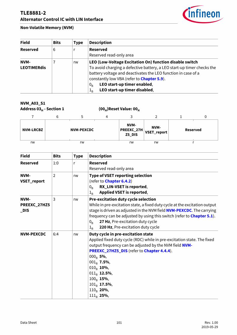
Data Sheet 101 Rev. 1.00 2019-05-29
TLE8881-2Alternator Control IC with LIN Interface
Non-Volatile Memory (NVM)
Reserved 6 r ReservedReserved read-only area
NVM-LEOTIMERdis
7 rw LEO (Low-Voltage Excitation On) function disable switchTo avoid charging a defective battery, a LEO start-up timer checks thebattery voltage and deactivates the LEO function in case of a constantly low VBA (refer to Chapter 5.9).0B LEO start-up timer enabled, 1B LEO start-up timer disabled,
NVM_A03_S1Address 03H - Section 1 (00H)Reset Value: 00H
7 6 5 4 3 2 1 0
NVM-LRCBZ NVM-PEXCDCNVM-
PREEXC_27HZ5_DIS
NVM-VSET_report Reserved
rw rw rw rw r
Field Bits Type DescriptionReserved 1:0 r Reserved
Reserved read-only area
NVM-VSET_report
2 rw Type of VSET reporting selection(refer to Chapter 6.4.2)0B RX_LIN-VSET is reported, 1B Applied VSET is reported,
NVM-PREEXC_27HZ5_DIS
3 rw Pre-excitation duty cycle selectionWhile in pre-excitation state, a fixed duty cycle at the excitation output stage is driven as adjusted in the NVM field NVM-PEXCDC. The carrying frequency can be adjusted by using this switch (refer to Chapter 5.1).0B 27 Hz, Pre-excitation duty cycle1B 220 Hz, Pre-excitation duty cycle
NVM-PEXCDC 6:4 rw Duty cycle in pre-excitation stateApplied fixed duty cycle (RDC) while in pre-excitation state. The fixed output frequency can be adjusted by the NVM field NVM-PREEXC_27HZ5_DIS (refer to Chapter 4.4.4).000B 5%, 001B 7.5%, 010B 10%, 011B 12.5%, 100B 15%, 101B 17.5%, 110B 20%, 111B 25%,
Field Bits Type Description

Data Sheet 102 Rev. 1.00 2019-05-29
TLE8881-2Alternator Control IC with LIN Interface
Non-Volatile Memory (NVM)
NVM-LRCBZ 7 rw Selection of the LRC blind zone in default operation stateSelection of the desired LRC blind zone while in default operation state (refer to Chapter 5.12).0B 3% / 6.25%, depending on NVM field NVM-LRCBZ_0_SEL1B 12%,
NVM_A03_S2Address 03H - Section 2 (00H)Reset Value: 00H
7 6 5 4 3 2 1 0
Reserved NVM-SSS
r rw
Field Bits Type DescriptionNVM-SSS 1:0 rw Self-start speed threshold
In case of absent LIN communication, an emergency start function assures proper operation of the regulator, if the TLE8881-2 is still in standby mode (no alternator rotation). The detection threshold of this emergency start function can be adjusted with this NVM field (physical parameter: nCUT2) (refer to Chapter 4.2).00B 2000 rpm, 01B 3000 rpm, 10B 4000 rpm, 11B 5000 rpm,
Reserved 7:2 r ReservedReserved read-only area
NVM_A04_S0Address 04H - Section 0 (00H)Reset Value: 00H
7 6 5 4 3 2 1 0
NVM-FROT_SEL NVM-HEO_ERR_EN
NVM-T_EL_ERR
NVM-LEO_ERR_EN NVM-LEO
rw rw rw rw rw
Field Bits Type Description

Data Sheet 103 Rev. 1.00 2019-05-29
TLE8881-2Alternator Control IC with LIN Interface
Non-Volatile Memory (NVM)
Field Bits Type DescriptionNVM-LEO 2:0 rw Default VLOW for LEO function (Low Voltage Excitation ON)
(refer to Chapter 5.9)000B 8.75 V, 001B 9.0 V, 010B 9.25 V, 011B 9.5 V, 100B 9.75 V, 101B 10.0 V, 110B 10.25 V, 111B 10.5 V,
NVM-LEO_ERR_EN
3 rw LEO/F-EL interaction settingEnable/disable interaction of LEO and the electrical error flag F-EL (refer to Chapter 4.5.3).0B Deactivate, LEO cannot set to the F-EL flag.1B Activate, LEO can set to the F-EL flag.
NVM-T_EL_ERR 4 rw Debounce time of electrical error flag (F-EL)Sets the debounce time for the electrical error flag (refer to Chapter 4.5.3).0B 250 ms, 1B 1000 ms,
NVM-HEO_ERR_EN
5 rw Overvoltage error flag switch(refer to Chapter 4.5.3)0B Deactivate, HEO does not set F-EL flag.1B Activate, HEO sets the error flag F-EL, if active.
NVM-FROT_SEL 7:6 rw Configuration for the mechanical error flag F-ROT(refer to Chapter 4.5.2)00B F-ROT set in pre-excitation, 01B F-ROT set in ComActive, pre-excitation and EXC-OFF, 10B Reserved, 11B Reserved,
NVM_A04_S1Address 04H - Section 1 (00H)Reset Value: 00H
7 6 5 4 3 2 1 0
NVM-CLIM NVM-HTG NVM-THT
rw rw r
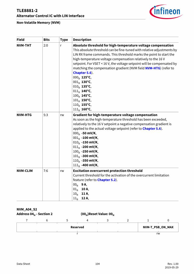
Data Sheet 104 Rev. 1.00 2019-05-29
TLE8881-2Alternator Control IC with LIN Interface
Non-Volatile Memory (NVM)
Field Bits Type DescriptionNVM-THT 2:0 r Absolute threshold for high-temperature voltage compensation
This absolute threshold can be fine-tuned with relative adjustments by LIN RX frame commands. This threshold marks the point to start the high-temperature voltage compensation relatively to the 16 V setpoint. For VSET < 16 V, the voltage setpoint will be compensated by matching the compensation gradient (NVM field NVM-HTG) (refer to Chapter 5.6).000B 125°C, 001B 130°C, 010B 135°C, 011B 140°C, 100B 145°C, 101B 150°C, 110B 155°C, 111B 160°C,
NVM-HTG 5:3 rw Gradient for high-temperature voltage compensationAs soon as the high-temperature threshold has been exceeded,relatively to the 16 V setpoint a negative compensation gradient is applied to the actual voltage setpoint (refer to Chapter 5.6).000B -50 mV/K, 001B -100 mV/K, 010B -150 mV/K, 011B -200 mV/K, 100B -250 mV/K, 101B -300 mV/K, 110B -350 mV/K, 111B -400 mV/K,
NVM-CLIM 7:6 rw Excitation overcurrent protection thresholdCurrent threshold for the activation of the overcurrent limitation feature (refer to Chapter 5.2).00B 9 A, 01B 10 A, 10B 11 A, 11B 12 A,
NVM_A04_S2Address 04H - Section 2 (00H)Reset Value: 00H
7 6 5 4 3 2 1 0
Reserved NVM-T_PSB_ON_MAX
r rw

Data Sheet 105 Rev. 1.00 2019-05-29
TLE8881-2Alternator Control IC with LIN Interface
Non-Volatile Memory (NVM)
Field Bits Type DescriptionNVM-T_PSB_ON_MAX
1:0 rw Maximum ON-time for PSB (Phase Signal Boost) functionRelating to Chapter 5.11, the phase signal boost function has a fixed OFF-time and an adjustable ON-time (DC = 100%). The PSB function helps to recover a low phase signal to assure a proper measurement of the phase signal.00B 155 ms, 01B 100 ms, 10B 45 ms, 11B 27 ms,
Reserved 7:2 r ReservedReserved read-only area
NVM_A05_S0Address 05H - Section 0 (00H)Reset Value: 00H
7 6 5 4 3 2 1 0
Reserved NVM-FEXLIM_PCLIM2 NVM-FEXLIM_EN NVM-FEXLIM_PCLIM1
r rw rw
Field Bits Type DescriptionNVM-FEXLIM_PCLIM1
2:0 rw Frequency dependent current limitation (FEXLIM) feature: PCLIM1 region(refer to Chapter 5.13)000B 5.5 A, 001B 6 A, 010B 6.5 A, 011B 7 A, 100B 7.5 A, 101B 8 A, 110B 8.5 A, 111B 9 A,
NVM-FEXLIM_EN
3 rw Enable/disable frequency dependent current limitation (FEXLIM) function(refer to Chapter 5.13)0B FEXLIM is disabled, 1B FEXLIM is enabled,

Data Sheet 106 Rev. 1.00 2019-05-29
TLE8881-2Alternator Control IC with LIN Interface
Non-Volatile Memory (NVM)
NVM-FEXLIM_PCLIM2
6:4 Frequency dependent current limitation (FEXLIM) feature: PCLIM2 region(refer to Chapter 5.13)000B 5.5 A, 001B 6 A, 010B 6.5 A, 011B 7 A, 100B 7.5 A, 101B 8 A, 110B 8.5 A, 111B 9 A,
Reserved 7 r ReservedReserved read-only area
NVM_A05_S1 Address 05H - Section 1 (00H)Reset Value: 00H
7 6 5 4 3 2 1 0
Reserved
r
Field Bits Type DescriptionReserved 7:0 r Reserved
Reserved read-only area
NVM_A05_S2 Address 05H - Section 2 (00H)Reset Value: 00H
7 6 5 4 3 2 1 0
Reserved
r
Field Bits Type DescriptionReserved 7:0 r Reserved
Reserved read-only area
NVM_A06_S0 Address 06H - Section 0 (00H)Reset Value: 00H
7 6 5 4 3 2 1 0
Reserved DC_EWMA_mode_DC0 NVM-VSET NVM-
LRCRT_1s
r rw rw rw
Field Bits Type Description
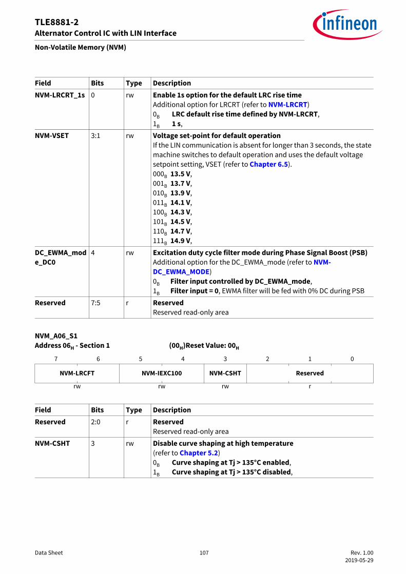
Data Sheet 107 Rev. 1.00 2019-05-29
TLE8881-2Alternator Control IC with LIN Interface
Non-Volatile Memory (NVM)
Field Bits Type DescriptionNVM-LRCRT_1s 0 rw Enable 1s option for the default LRC rise time
Additional option for LRCRT (refer to NVM-LRCRT)0B LRC default rise time defined by NVM-LRCRT, 1B 1 s,
NVM-VSET 3:1 rw Voltage set-point for default operationIf the LIN communication is absent for longer than 3 seconds, the statemachine switches to default operation and uses the default voltage setpoint setting, VSET (refer to Chapter 6.5).000B 13.5 V, 001B 13.7 V, 010B 13.9 V, 011B 14.1 V, 100B 14.3 V, 101B 14.5 V, 110B 14.7 V, 111B 14.9 V,
DC_EWMA_mode_DC0
4 rw Excitation duty cycle filter mode during Phase Signal Boost (PSB)Additional option for the DC_EWMA_mode (refer to NVM-DC_EWMA_MODE)0B Filter input controlled by DC_EWMA_mode, 1B Filter input = 0, EWMA filter will be fed with 0% DC during PSB
Reserved 7:5 r ReservedReserved read-only area
NVM_A06_S1Address 06H - Section 1 (00H)Reset Value: 00H
7 6 5 4 3 2 1 0
NVM-LRCFT NVM-IEXC100 NVM-CSHT Reserved
rw rw rw r
Field Bits Type DescriptionReserved 2:0 r Reserved
Reserved read-only area
NVM-CSHT 3 rw Disable curve shaping at high temperature(refer to Chapter 5.2)0B Curve shaping at Tj > 135°C enabled, 1B Curve shaping at Tj > 135°C disabled,

Data Sheet 108 Rev. 1.00 2019-05-29
TLE8881-2Alternator Control IC with LIN Interface
Non-Volatile Memory (NVM)
NVM-IEXC100 5:4 rw Minimum excitation current at 100% DC to avoid open load detection(refer to Chapter 5.2)00B 0.75 A, 01B 1 A, 10B 1.25 A, 11B 1.50 A,
NVM-LRCFT 7:6 rw LRC fall-timeThe falling gradient is defined as the ramp-down time to go from 100%to 0% DC value. The falling gradient is not seen at the output DMOS, butis only calculated internally (refer to Chapter 5.12).00B 1 s, 01B 2 s, 10B 2.5 s, 11B 3 s,
NVM_A06_S2Address 06H - Section 2 (00H)Reset Value: 00H
7 6 5 4 3 2 1 0
Reserved
r
Field Bits Type DescriptionReserved 7:0 r Reserved
Reserved read-only area
NVM_A07_S0Address 07H - Section 0 (00H)Reset Value: 00H
7 6 5 4 3 2 1 0
Reserved NVM-LRCDIS NVM-Speed_TH
r rw rw
Field Bits Type Description
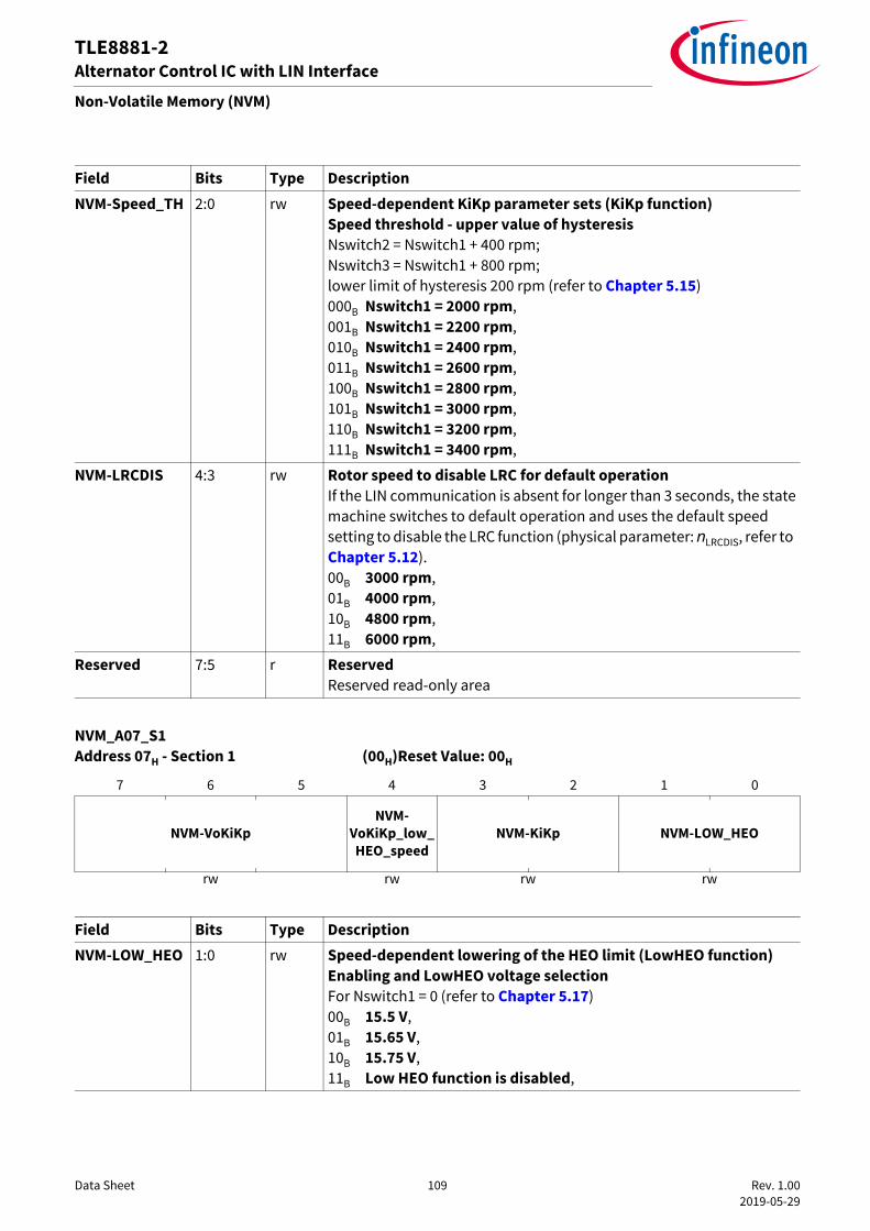
Data Sheet 109 Rev. 1.00 2019-05-29
TLE8881-2Alternator Control IC with LIN Interface
Non-Volatile Memory (NVM)
Field Bits Type DescriptionNVM-Speed_TH 2:0 rw Speed-dependent KiKp parameter sets (KiKp function)
Speed threshold - upper value of hysteresisNswitch2 = Nswitch1 + 400 rpm;Nswitch3 = Nswitch1 + 800 rpm;lower limit of hysteresis 200 rpm (refer to Chapter 5.15)000B Nswitch1 = 2000 rpm, 001B Nswitch1 = 2200 rpm, 010B Nswitch1 = 2400 rpm, 011B Nswitch1 = 2600 rpm, 100B Nswitch1 = 2800 rpm, 101B Nswitch1 = 3000 rpm, 110B Nswitch1 = 3200 rpm, 111B Nswitch1 = 3400 rpm,
NVM-LRCDIS 4:3 rw Rotor speed to disable LRC for default operationIf the LIN communication is absent for longer than 3 seconds, the statemachine switches to default operation and uses the default speedsetting to disable the LRC function (physical parameter: nLRCDIS, refer to Chapter 5.12).00B 3000 rpm, 01B 4000 rpm, 10B 4800 rpm, 11B 6000 rpm,
Reserved 7:5 r ReservedReserved read-only area
NVM_A07_S1Address 07H - Section 1 (00H)Reset Value: 00H
7 6 5 4 3 2 1 0
NVM-VoKiKpNVM-
VoKiKp_low_HEO_speed
NVM-KiKp NVM-LOW_HEO
rw rw rw rw
Field Bits Type DescriptionNVM-LOW_HEO 1:0 rw Speed-dependent lowering of the HEO limit (LowHEO function)
Enabling and LowHEO voltage selectionFor Nswitch1 = 0 (refer to Chapter 5.17)00B 15.5 V, 01B 15.65 V, 10B 15.75 V, 11B Low HEO function is disabled,

Data Sheet 110 Rev. 1.00 2019-05-29
TLE8881-2Alternator Control IC with LIN Interface
Non-Volatile Memory (NVM)
NVM-KiKp 3:2 rw KiKp function configuration(refer to Chapter 5.15)00B KiKp disabled, 01B Simple KiKp function with KiKp set = slowest, 10B Simple KiKp function with KiKp set = slower, 11B Three stage KiKp function,
NVM-VoKiKp_low_HEO_speed
4 rw Voltage dependent KiKp function (VoKiKp) speed dependencyActivates / deactivates the speed dependency for the VoKiKp and LowHEO functions (refer to Chapter 5.16).0B Speed dependency enabled, 1B Speed dependency disabled,
NVM-VoKiKp 7:5 rw Voltage dependent KiKp function (VoKiKp function) configuration Enabling and VoKiKp up thresholdThe VoKiKp down threshold is 0.1 V lower. For options 101B, 110B and 111B the VoKiKp down threshold is 0.1V lower than the positive value and 0.1V higher than the negative value (refer to Chapter 5.16). 000B VoKiKp disabled, 001B 0.35 V, 010B 0.5 V, 011B 0.65 V, 100B 0.8 V, 101B +/- 0.5V, VoKiKp is activated for an upper and lower threshold110B +/- 0.75V, VoKiKp is activated for an upper and lower threshold111B +/- 1V, VoKiKp is activated for an upper and lower threshold
NVM_A07_S2Address 07H - Section 2 (00H)Reset Value: 00H
7 6 5 4 3 2 1 0
Reserved NVM-LOCK_EN Reserved
rw r
Field Bits Type DescriptionReserved 0 r Reserved
Reserved read-only area
NVM-LOCK_EN 1 rw Enable NVM LockSetting this NVM field makes the NVM write-protected and protect it from any modification afterwards.
Note: Once this bit is set, the NVM will get write-protected. It is not possible to release the write-protection once it has been set.
0B NVM can be programmed, 1B NVM is locked,
Field Bits Type Description

Data Sheet 111 Rev. 1.00 2019-05-29
TLE8881-2Alternator Control IC with LIN Interface
Non-Volatile Memory (NVM)
Reserved 7:2 ReservedReserved read-only area
Field Bits Type Description

Data Sheet 112 Rev. 1.00 2019-05-29
TLE8881-2Alternator Control IC with LIN Interface
Application information
10 Application information
Note: The following information is given as a hint for the implementation of the device only and shall not be regarded as a description or warranty of a certain functionality, condition or quality of the device.
This is the description how the TLE8881-2 is used in its alternator environment.
Figure 26 Application diagram
Note: This is a very simplified example of an application circuit. The function must be verified in the real application.
The TLE8881-2 regulates the alternator output to an adjustable reference voltage. The regulation is achievedby varying the magnetization in the alternator. The magnetization is dependent on the current in the rotorwinding (excitation). The current is dependent on the duty cycle of the excitation high-side output (terminalEXC).The TLE8881-2 supply (VBA) is connected to the alternator output. The filtered supply voltage is the feedbackvoltage used by the control circuit.One of three stator winding voltages (PH) is connected to the TLE8881-2. The phase input is used for the rotorspeed measurement and stator monitoring, as well as the self-start detection.
AlternatorControl IC
Battery
B+A
PH
EXC
GND
VBA
Alternator
GND
B+A
ECU (Engine or Energy Control Unit)
Alternator speed
Engine
VehicleLoads
LIN
LIN interface
BUS

Data Sheet 113 Rev. 1.00 2019-05-29
TLE8881-2Alternator Control IC with LIN Interface
Application information
10.1 EMC and ESDISO and ESD pulses are applied to the alternator. The TLE8881-2 does not see all disturbances at its pins dueto connectors, the alternator and the diodes. The sensitivity depends on the TLE8881-2 and the completealternator system.
Figure 27 Application overview for EMC
The stated intend is to ensure all EMC and ESD requirements without any TLE8881-2 external devices. The external passive devices indicate their possible use only.In the car system, the TLE8881-2 will be used as a LIN-Slave.The device will be tested or referenced according to the VDA Test Spec “2009-12-02 Common EMC-requirements on LIN-Interfaces” at IBEE Zwickau.
10.2 Further application information• For further information you may contact https://www.infineon.com
B+A
GND
ALTERNATOR
B+A
GNDBRUSHHOLDER
EXC
PH VBA
LINAlternator Control IC

Data Sheet 114 Rev. 1.00 2019-05-29
TLE8881-2Alternator Control IC with LIN Interface
Package information
11 Package information
Figure 28 PG-TO-220-5-12 Straight Leads1)
Green Product (RoHS compliant)To meet the world-wide customer requirements for environmentally friendly products and to be compliantwith government regulations the device is available as a green product. Green products are RoHS-Compliant(i.e Pb-free finish on leads and suitable for Pb-free soldering according to IPC/JEDEC J-STD-020).
Further information on packageshttps://www.infineon.com/packages
1) Dimensions in mm
A
BA0.25 M
9.9 ±0.2
2.8
1)15
.65±0
.3
12.95
0...0.15
±0.11.274.4
B
9.25±
0.20.05
C
±0.2
17±0
.3
8.5 1)
10 ±0.2
3.7 -0.15
C
2.40.5 ±0.1
13±0
.5±0.5
110...0.3
1.74 x5 x ±0.10.8
2.4
All metal surfaces tin plated, except area of cut.Metal surface min. X = 7.25, Y = 12.3Typical1)

Data Sheet 115 Rev. 1.00 2019-05-29
TLE8881-2Alternator Control IC with LIN Interface
Revision history
12 Revision history
Revision Date Changes1.00 2019-05-29 Datasheet released

TrademarksAll referenced product or service names and trademarks are the property of their respective owners.
Edition 2019-05-29Published by Infineon Technologies AG81726 Munich, Germany
© 2019 Infineon Technologies AG.All Rights Reserved.
Do you have a question about any aspect of this document?Email: [email protected]
Document referenceDoc_Number
IMPORTANT NOTICEThe information given in this document shall in noevent be regarded as a guarantee of conditions orcharacteristics ("Beschaffenheitsgarantie"). With respect to any examples, hints or any typicalvalues stated herein and/or any information regardingthe application of the product, Infineon Technologieshereby disclaims any and all warranties and liabilitiesof any kind, including without limitation warranties ofnon-infringement of intellectual property rights of anythird party. In addition, any information given in this document issubject to customer's compliance with its obligationsstated in this document and any applicable legalrequirements, norms and standards concerningcustomer's products and any use of the product ofInfineon Technologies in customer's applications. The data contained in this document is exclusivelyintended for technically trained staff. It is theresponsibility of customer's technical departments toevaluate the suitability of the product for the intendedapplication and the completeness of the productinformation given in this document with respect tosuch application.
For further information on technology, delivery termsand conditions and prices, please contact the nearestInfineon Technologies Office (www.infineon.com).
WARNINGSDue to technical requirements products may containdangerous substances. For information on the typesin question please contact your nearest InfineonTechnologies office.
Except as otherwise explicitly approved by InfineonTechnologies in a written document signed byauthorized representatives of Infineon Technologies,Infineon Technologies’ products may not be used inany applications where a failure of the product or anyconsequences of the use thereof can reasonably beexpected to result in personal injury.