allegro pcb design 610/620 - flowcad · 2006-01-30 · cadence ®allegro pcb design 610 and...
TRANSCRIPT

DATASHEET
ALLEGRO PCB DESIGN 610/620HIGH-SPEED, CONSTRAINT-DRIVEN PCB DESIGN
Cadence® Allegro® PCB Design 610 and 620—600 series products within theAllegro system interconnect design platform—are complete, high-performancePCB design suites. Through leading-edge technology, they provide an interactive,constraint-driven environment for creating and editing complex, multilayer, high-speed, high-density PCBs. They allow users to define, manage, and validatecritical high-speed signals at any stage of the design process and master today'smost challenging PCB design issues. The result—increased productivity, shorterdesign cycles, and faster time to volume production.
THE ALLEGRO SYSTEMINTERCONNECT DESIGNPLATFORMThe Cadence Allegro systeminterconnect design platformenables collaborative design ofhigh-performance interconnectacross IC, package, and PCB domains.The platform’s unique co-designmethodology optimizes systeminterconnect — between I/O buffersand across ICs, packages, and PCBs —to eliminate hardware re-spins,decrease costs, and reduce designcycles. The Allegro constraint-drivenflow offers advanced capabilities fordesign capture, signal integrity, andphysical implementation. With silicondesign-in kits, IC companies shortennew device adoption time and systemscompanies accelerate PCB design cyclesfor rapid time to profit. Supported bythe Cadence Encounter™ and Virtuoso®
platforms, the Allegro co-designmethodology ensures effective designchain collaboration.
The Allegro system interconnect design platform
IC package andSiP design
PCB design
I/O bufferdesign IC design
Packagedesign-in kit
Silicondesign-in kit
On-target, on-timesystem interconnectInterconnect
models
I/O bufferIP
Virtual systeminterconnect
model
Verify
Build
Correlate
Specify
Explore
Design
Implement
2
ALLEGRO PCB DESIGN 620The pressure to shorten design-cycletimes is heightened by the growingdeployment of globally disperseddesign teams. With PCB designpartitioning technology, multiplePCB designers working concurrentlyon a layout share access to a singledatabase, regardless of team proximity.This can dramatically reduce overalldesign cycles and accelerate the designprocess to help meet project schedules.
FEATURES
A COMPLETE HIGH-SPEED PCBDESIGN ENVIRONMENT
Allegro PCB Design 610 and 620 includedesign capture, librarian tools, AllegroConstraint Manager, PCB Editor, anauto/interactive router, interfaces forRF co-design, manufacturing, andmechanical CAD, and translators forother PCB systems.
If you’re designing PCBs that need morethan 25% of the design constrained toensure signal integrity performance,and you want to adopt a simulation-driven design flow, Allegro PCB Design610 and 620 are the obvious choices.
It has the ability to define, eithermanually or through simulation, acomprehensive set of electrical ruleswithin Constraint Manager, enablingconstraint-driven layout—this shortensthe design cycle by eliminating time-consuming and frustrating layout-simulate-fix iterations.
FRONT-TO-BACK CONSTRAINTMANAGEMENT SYSTEM
The exclusive Allegro ConstraintManager from Cadence is a front-to-back constraint management systemthat provides a real-time display ofhigh-speed rules, such as differentialsignals, length, timing, and electricalconstraints. The status of these rules isdisplayed in real time, based on thecurrent state of the design. Thiseliminates the need for constrainttranslation, forward and backwardannotation, or static design rulechecking.
REUSABLE INTERCONNECTTOPOLOGY TEMPLATE
Reusable interconnect topologytemplate-driven place and routeensures that physical implementationmeets simulation-derived requirementsand can be shaped and reused acrossmultiple designers and projects. Thisensures implementation consistency.
ADVANCED INTERACTIVE ETCHCREATION/EDITING CAPABILITIES
Powerful shape-based shove/huginteractive etch creation/editingprovides the designer with a highlyproductive interconnect environmentwhile providing real-time, heads-updisplays of length and timing margins.
DESIGN SYNCHRONIZATION
Design synchronization boostsproductivity through concurrent designby enabling the designer to analyzethe schematic and PCB and highlightdifferences by category.
The designer can then decide whichchanges are to be observed and theappropriate system will automaticallybe updated.
DESIGN REUSE MODELS
Team-based design reuse modules atthe schematic and board level allowdesigners to easily share commoncircuitry and to refresh modules toincorporate the latest updates.
MULTIGIGABIT DESIGN ANDIMPLEMENTATION
Differential signaling technologyenables the designer to reduce designtime by introducing the ability todefine differential signals as uniqueentities. You can perform simulationto derive constraints, define acomprehensive set of rules withinConstraint Manger, and then use thoserules to drive placement, automatic,and interactive routing. This eliminatesnumerous iterations and increases theprobability of first-time design success.
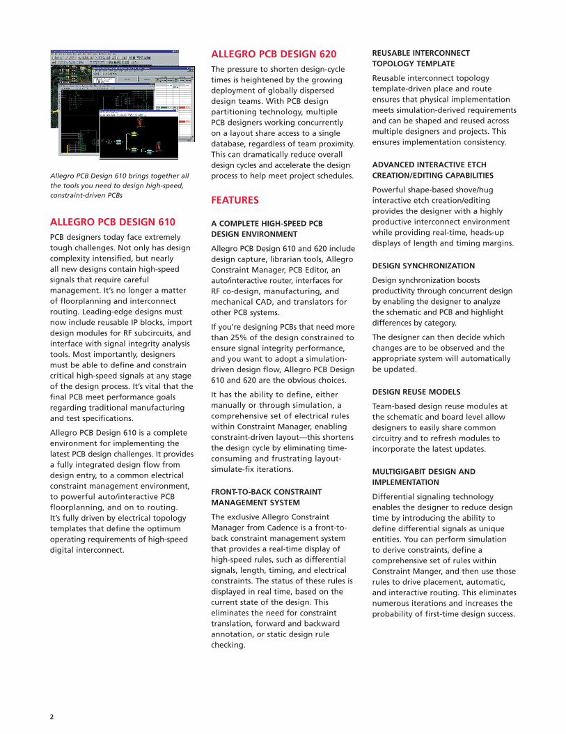
Allegro PCB Design 610 brings together allthe tools you need to design high-speed,constraint-driven PCBs
ALLEGRO PCB DESIGN 610PCB designers today face extremelytough challenges. Not only has designcomplexity intensified, but nearlyall new designs contain high-speedsignals that require carefulmanagement. It’s no longer a matterof floorplanning and interconnectrouting. Leading-edge designs mustnow include reusable IP blocks, importdesign modules for RF subcircuits, andinterface with signal integrity analysistools. Most importantly, designersmust be able to define and constraincritical high-speed signals at any stageof the design process. It’s vital that thefinal PCB meet performance goalsregarding traditional manufacturingand test specifications.
Allegro PCB Design 610 is a completeenvironment for implementing thelatest PCB design challenges. It providesa fully integrated design flow fromdesign entry, to a common electricalconstraint management environment,to powerful auto/interactive PCBfloorplanning, and on to routing.It’s fully driven by electrical topologytemplates that define the optimumoperating requirements of high-speeddigital interconnect.
3
CONCURRENT DESIGN METHODOLOGY
PCB design partitioning technologyprovides a concurrent design method-ology for faster time to market andreduction in layout time. Manualworkarounds to address multi-userchallenges are time consuming,slow and prone to error. Designerscan partition designs into multiplesections or areas for layout andediting by several design-teammembers. Designers are able to viewall partitioned sections and update thedesign view for monitoring the statusand progress of other users’ sections.
A FULL SUITE OF PCBDESIGN TOOLSAllegro PCB Design 610 and 620 arestocked with the major tools you needto design complex, high-speed PCBs:
• Allegro Constraint Manager forelectrical constraint definition,management, and analysis
• Librarian functionality for library partcreation and management
• Allegro PCB Editor for high-speed,constraint-driven, board-levelplacement, routing, and manufacturingoutput
• Allegro PCB Router 610 for high-speed, constraint-driven, shape-based routing
Your choice of design entry tools:
• Allegro Design Entry HDL forhierarchical design entry supportingany combination of graphicalschematics and hardware descriptionlanguages with design reuse andvariants-based design capabilities
– or –
• Allegro Design Entry CIS withintegrated component management
PRODUCTIVITYENHANCEMENTSIn addition to the standard toolset,Allegro PCB Design 610 and 620provide the following capabilities aspart of its overall configuration:
• PCB database import capabilitiesfor OrCAD Layout®, Mentor PowerPCB,and Altium P-CAD®
• Mechanical interfaces for DXF, IDF,a generic MCAD interface toolkit
• Library-level design reuse moduledefinition for IP sharing acrossdesign teams
• Variant design for multiple designconfigurations from a single designmaster
• Rules Checker option (CheckPlus)for advanced custom schematic designrule checking (available with AllegroDesign Entry HDL only)
• RF subcircuit design import fromAgilent ADS (formerly Agilent EEsof)for schematic and PCB layout
• Topology extraction for simulation(with Allegro PCB SI), application,and creation
• Valor ODB++ output and viewing usingthe included Valor Universal Viewer
CONSTRAINT AND RULES-DRIVEN SYSTEMAllegro PCB Design 610 and 620support an extensive range of designrules to meet present and future PCBdesign and manufacturing needs. Rulescan be defined and adhered to at anylevel of the design process with real-time online design rule checking (DRC).Rules can be defined by part, net,group, area, and layer. Full supportis provided for blind and buried vias,including extensive support forMicrovia structures. In both breadthof functionality and performance,Allegro PCB Design 610 and 620 arethe industry’s leading constraint- andrules-driven system. The constraint-
and rules-driven approach is aconsiderable improvement over thetraditional design-then-analyzeapproach.
Cadence has extended the twoconcepts of rules-driven design andin-process analysis to create a systemin which important design ortechnology considerations are definedin advance and are automaticallychecked throughout the designprocess. The result is shorter designcycles and optimized performance,quality, and cost.
ALLEGRO CONSTRAINTMANAGERAt the heart of Allegro PCB Design 610and 620 is the powerful, spreadsheet-based Allegro Constraint Manger.
Constraint Manager provides a real-time display of high-speed rules andtheir status (based on the current stateof the design) and is available at allstages of the design process. Eachworksheet provides a spreadsheetinterface that enables the user tocapture, manage, and validate thedifferent rules in a hierarchical fashion.Constraint Manager enables designersto group all of the high-speedconstraints for a collection of signalsto form an electrical constraint set thatis then associated with those nets tomanage their actual implementation.A separate DRC worksheet displays allAllegro PCB Editor DRCs along withdetails about each DRC item.
This powerful instrument allowsdesigners to graphically create, edit,and review constraint sets as graphicaltopologies that act as electronicblueprints of an ideal implementationstrategy. Once the constraints arepresent in the database, they are usedto drive the placement and routingprocesses for those signals. Hierarchicalconstraint management means thatthe same constraints can be applied toa collection of signals and thenoverridden on a case-by-case basiswhere appropriate.
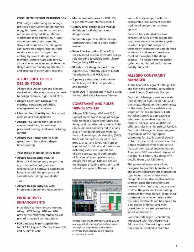
Constraint Manager is completelyintegrated with the Allegro PCBEditor — the different high-speedrules can be checked in real time
Allegro Constraint Manager allows you tomanage all of your high-speed constraintsthrough an easy-to-use spreadsheetinterface that changes color, makingerrors easy to spot

4
as the design process proceeds, withthe results presented as part of theConstraint Manager spreadsheets. Anydesign parameters that do not meettheir associated constraint values arehighlighted. Constraint Manager alsointegrates the results of signalintegrity analysis, allowing designersto manage simulation-based electricalconstraints. By combining knowledgeof bus operating speeds withcomponent timing data and theresults of signal integrity analysis, onespreadsheet shows the designerwhether or not critical system-leveltiming requirements will be met.
At any point during the design phase,users can launch the ConstraintManager to add, view, and managehigh-speed constraint informationassociated with the design. Thisapplies to design entry, interconnectexploration and simulation, as wellas physical board layout and designvalidation. The spreadsheet presentstwo views of the constraint informationin the database. One view allowsdesigners to see the different electricalconstraint sets present in the databaseand their associated constraint values.The other view presents the differentnets contained in the system with thenames of the constraint sets associatedwith those nets (if any), and theirassociated constraint values. ConstraintManager also displays the results ofdesign analysis in real time alongsidethe constraint values in the spreadsheet,and color codes the results to indicatesuccess or failure. This allows you to seethe impact of any design changesimmediately in the spreadsheet.
The DRC workbook itemizes fourclasses of DRCs: Electrical, Spacing,Physical and Design. Each worksheetprovides information about theDRC in terms of quantity, location,required and actual values, constraintset references and objects affected.Clicking on the X,Y coordinatechanges the view in the PCB Editordisplay to the DRC location.
The ability to combine automatic andmanual constraint definition is ideal forhigh-speed designs. With the rulesembedded in the design, designers canconcentrate on optimizing the physicallayout for size, routability, andmanufacturability, while the engineer’sperformance requirements areautomatically observed by the software.
PART CREATION ANDMANAGEMENTLibrarian functionality assembles thetools to tackle the three critical areasof part management: creation,packaging, and qualification.
Creation — Part Developer letsyou create, edit, and test logicalcomponent data (schematic symbol,physical pin data, and part number).
Packaging — With the Package DesignEditor, the librarian functionalitygenerates the physical package, boardoutlines, and detailed dimensiondrawings. You can quickly creategraphical definitions of large, high-pincount devices, such as BGAs and PGAs.You can also establish designconstraints, drawing details such ascross-sections, and othermanufacturing output parameters.The Padstack Editor is a completelygraphical environment for defining,reviewing, and editing multilayerpadstacks. It provides both cross-section and plan views, helping youcreate padstacks quickly and correctlywithout having to generate testdesigns or decipher textual reports.
Qualification — To ensure parts arecreated correctly and qualified in asystematic, consistent manner, use theLibrary Explorer. It sets up one area
strictly for parts you are creatingor modifying, and another area forparts fully qualified for production.Comprehensive error checkingroutines help you ensure newparts actually work.
ALLEGRO PCB DESIGN 610AND 620: THE BEST DESIGNENTRY TOOLSAllegro PCB Design 610 and 620 offertwo design entry solutions, each withunique strengths and approaches.Choose between Allegro Design EntryHDL or Allegro Design Entry CIS,whichever best suits your needs andwork style.
ALLEGRO DESIGN ENTRY HDLAre you ready to move beyonddrawing schematics to the morepowerful and efficient methodsof language-based systems design,variant-based design, and design reuseat the team level? Do you want tofully integrate your design tools intoyour production infrastructure (insteadof the other way around), and tunethem to your specific needs andpreferences? Do you need to definehigh-speed constraints during designentry? Define topology specificationsbased on simulation? Then you’reready for Allegro Design Entry HDL(DE-HDL).
The mixed-level environment ofDE-HDL allows you to build designsusing any combination of behavioraland structural descriptions. Designedespecially to support a top-downmethodology, DE-HDL is perfectlyPadstack Editor for rapid graphical
padstack creation
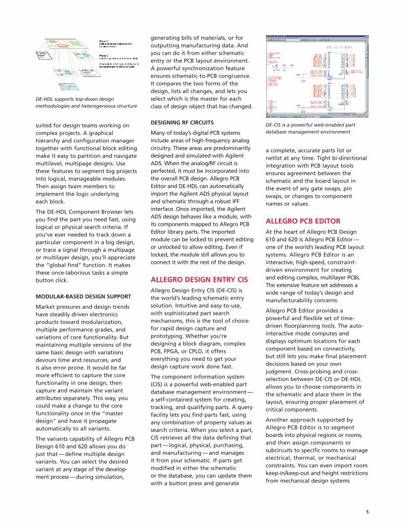
DE-HDL provides a powerful environmentfor language/structure design capture
5
suited for design teams working oncomplex projects. A graphicalhierarchy and configuration managertogether with functional block editingmake it easy to partition and navigatemultilevel, multipage designs. Usethese features to segment big projectsinto logical, manageable modules.Then assign team members toimplement the logic underlyingeach block.
The DE-HDL Component Browser letsyou find the part you need fast, usinglogical or physical search criteria. Ifyou’ve ever needed to track down aparticular component in a big design,or trace a signal through a multipageor multilayer design, you’ll appreciatethe “global find” function. It makesthese once-laborious tasks a simplebutton click.
MODULAR-BASED DESIGN SUPPORT
Market pressures and design trendshave steadily driven electronicsproducts toward modularization,multiple performance grades, andvariations of core functionality. Butmaintaining multiple versions of thesame basic design with variationsdevours time and resources, andis also error prone. It would be farmore efficient to capture the corefunctionality in one design, thencapture and maintain the variantattributes separately. This way, youcould make a change to the corefunctionality once in the “masterdesign” and have it propagateautomatically to all variants.
The variants capability of Allegro PCBDesign 610 and 620 allows you dojust that — define multiple designvariants. You can select the desiredvariant at any stage of the develop-ment process — during simulation,
generating bills of materials, or foroutputting manufacturing data. Andyou can do it from either schematicentry or the PCB layout environment.A powerful synchronization featureensures schematic-to-PCB congruence.It compares the two forms of thedesign, lists all changes, and lets youselect which is the master for eachclass of design object that has changed.
DESIGNING RF CIRCUITS
Many of today’s digital PCB systemsinclude areas of high-frequency analogcircuitry. These areas are predominantlydesigned and simulated with AgilentADS. When the analog/RF circuit isperfected, it must be incorporated intothe overall PCB design. Allegro PCBEditor and DE-HDL can automaticallyimport the Agilent ADS physical layoutand schematic through a robust IFFinterface. Once imported, the AgilentADS design behaves like a module, withits components mapped to Allegro PCBEditor library parts. The importedmodule can be locked to prevent editingor unlocked to allow editing. Even iflocked, the module still allows you toconnect it with the rest of the design.
ALLEGRO DESIGN ENTRY CISAllegro Design Entry CIS (DE-CIS) isthe world’s leading schematic entrysolution. Intuitive and easy-to-use,with sophisticated part searchmechanisms, this is the tool of choicefor rapid design capture andprototyping. Whether you’redesigning a block diagram, complexPCB, FPGA, or CPLD, it offerseverything you need to get yourdesign capture work done fast.
The component information system(CIS) is a powerful web-enabled partdatabase management environment —a self-contained system for creating,tracking, and qualifying parts. A queryfacility lets you find parts fast, usingany combination of property values assearch criteria. When you select a part,CIS retrieves all the data defining thatpart — logical, physical, purchasing,and manufacturing — and managesit from your schematic. If parts getmodified in either the schematicor the database, you can update themwith a button press and generate
a complete, accurate parts list ornetlist at any time. Tight bi-directionalintegration with PCB layout toolsensures agreement between theschematic and the board layout inthe event of any gate swaps, pinswaps, or changes to componentnames or values.
ALLEGRO PCB EDITORAt the heart of Allegro PCB Design610 and 620 is Allegro PCB Editor —one of the world’s leading PCB layoutsystems. Allegro PCB Editor is aninteractive, high-speed, constraint-driven environment for creatingand editing complex, multilayer PCBs.The extensive feature set addresses awide range of today’s design andmanufacturability concerns.
Allegro PCB Editor provides apowerful and flexible set of time-driven floorplanning tools. The auto-interactive mode computes anddisplays optimum locations for eachcomponent based on connectivity,but still lets you make final placementdecisions based on your ownjudgment. Cross-probing and cross-selection between DE-CIS or DE-HDLallows you to choose components inthe schematic and place them in thelayout, ensuring proper placement ofcritical components.
Another approach supported byAllegro PCB Editor is to segmentboards into physical regions or rooms,and then assign components orsubcircuits to specific rooms to manageelectrical, thermal, or mechanicalconstraints. You can even import roomkeep-in/keep-out and height restrictionsfrom mechanical design systems
DE-CIS is a powerful web-enabled partdatabase management environment
DE-HDL supports top-down designmethodologies and heterogeneous structure
6
using DXF or IDF data formats. Duringsubcircuit floorplanning, it’s oftenbeneficial to place the componentsprior to floorplanning as a selection“palette.” The QuickPlace utility withinAllegro PCB Editor allows you to selectunplaced components around the PCBoutline based on specified criteria.
Cadence pioneered the concept ofrules-driven design with the AllegroPCB Editor. Component placementconstraints, device grouping, andrequired trace widths for critical netsare encoded along with the designlogic during schematic capture. All ofthis data is imported into the layoutenvironment to be used duringplacement and routing.
EXTENDED TIMING AND PATHS Z-AXIS DELAY
Extended timing and paths Z-axisdelay increase the precision of high-speed routing. The ‘Z’ dimension ofvias and through hole pins can now beincluded in routing calculations. Also,extended timing paths; which are thedistances from a package’s externalpin to the package’s internal die pincan now be included in routingcalculations. These constraints onlywork in conjunction with the min/maxpropagation, relative propagation ordifferential pair phase controlelectrical rules.
For Z-axis delay, the length of theconductive path of the hole is includedin the actual length for the applied rule.The Z-dimension length is calculated byaccumulating the number of the copperlayer and dielectric thicknesses over theconductive path of the hole.
For extended timing paths, the lengthof a package’s internal routing and/orwire bonds are from the external pinto the internal die connections and areincluded in the actual length for theapplied rule.
ADVANCED FLOORPLANNING AND PRE-FLOORPLANNING WITH QUICKPLACE
The Allegro PCB Editor’s constraint- and rules-driven methodology drives apowerful and flexible set of placement
capabilities, including interactive andautomatic component placement. You can divide boards into separatesections called “rooms.” Components orsubcircuits can be assigned to a specificroom by the engineer or designerduring design entry or floorplanning.Each room can have a differentplacement grid if desired. The QuickPlacefeature allows the designer to filterand pre-group functional groups ofcomponents and stack them around the board periphery. Components canbe filtered and selected by referencedesignator, device package/footprintstyle, associated net name, part number,or the schematic sheet/page number.
With real-time Design-for-Assemblyanalysis, Allegro PCB Editor offers real-time package-to-package clearancechecking during interactive componentplacement. Driven from a 2-dimensionalspreadsheet array of classes andpackage instances, real-time feedbackprovides minimum clearance require-ments based on the package’s side toside, side to end or end to end profiles.With thousands of components ontoday’s boards, real time DFA analysisfeedback increases the designer’sproductivity and efficiency byplacing components to corporateor EMS guidelines and helps reducethe dependency on referencingspecifications or interfacing with thirdparty manufacturing systems.
Allegro PCB Editor and the ConstraintManager provide real-time graphicalfeedback of interconnect timingmargins during interactive floor-planning. Timing constraints andmargins can be defined interactively
or created through interconnectsolution-space analysis using AllegroPCB SI. This lets the PCB designersimultaneously place devices foroptimum routability, manufacturability,and signal timing.
INTELLIUSE INTERACTIVE ETCH EDITING
When it comes to interconnectimplementation, Allegro PCB Editorstands alone. With IntelliUSE routing,powerful interactive features provide“controlled automation” to maintainuser control while maximizingproductivity. IntelliUSE provides real-time, shape-based, any angle,push/shove routing — enabling thedesigner to choose between “shove-preferred” and “hug-preferred”modes. The real-time, embedded,shape-based routing engine optimizesthe route by either pushing obstaclesor contour-following obstacles whiledynamically jumping vias orcomponent pins. Custom, controllable,on-the-fly smoothing automaticallytunes the route for manufacturabilityduring routing or route editing. Anyinterconnect that has high-speedconstraints provides the designer witha real-time, graphical “heads-up”display that shows how much timing“slack” remains. IntelliUSE alsoprovides the ability to perform grouprouting on multiple nets andinteractive tuning of nets with high-speed length or delay constraints.Layer Set aware routing enhancesinteractive routing for high-speed,impedance and reference planecontrol. With a net constrained toa set for routing, the active andalternate subclass fields are intelligentlymapped to layers within a set to insure
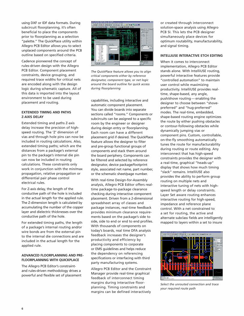
The QuickPlace feature allows you to aligncritical components either by referencedesignator, component type, or net logicaround the board outline for quick accessduring floorplanning
Select the unrouted connection and traceyour required route path
7
routing is locked on a layer or layerpair or group of layers. Preferredlayers are accentuated making layerchoices more of an intuitive selection.
Shove-preferred mode — Allows youto construct the optimum interconnectpath while the real-time, shape-basedrouter takes care of dynamicallypushing obstacles. Routes willautomatically jump over pins or vias.
Hug-preferred mode — The perfectsolution for ECOs or for where adatabus needs to be constructed. Inhug-preferred mode, the routercontour follows other interconnect as apriority and only pushes aside or jumpsobstacles when it has no other option.
Hug-only mode — The ‘Hug Only’option, available with add connect,slide and vertex, will perform similarto the ‘hug preferred’ mode butwithout the push-n-shove aggressionon other etch objects.
DYNAMIC SHAPES
Offers real-time copper pourplowing/healing functionality. Shape
parameters can be applied at threedifferent levels. Parameters are structuredinto global, shape instance, and objectlevel hierarchy. Traces, vias, andcomponents added to a dynamic shapewill automatically plow and void throughthe shape. When items are removed,the shape will automatically fill backin. Dynamic shapes do not requirebatch auto-voiding or other post-processing steps after edits are made.
PREPARING FOR MANUFACTURING
A major trend in high-volumeproduction designs is the use ofcomplex powerplanes in order to keeplayer counts to a minimum and reducecosts. To meet these challenges, AllegroPCB Editor provides some of theindustry’s most powerful andcomprehensive powerplane creationand editing capabilities. These includeuser-defined split planes, negative orpositive views of internal layer planes,and extensive options for user-definedcopper pour partial-planes. Fullpowerplanes provide the designerwith the unique ability to view andanalyze negatively implementedplanes as a positive image with fullWYSIWYG control.
But all this functionality andsophistication is of little value if thepath to PCB manufacturing is toonarrow. Allegro PCB Editor tackles thisside of the equation by giving you awide range of manufacturing outputs.Allegro PCB Editor can generate a fullsuite of photo-tooling, bare-boardfabrication and test outputs, includingGerber 274x, NC drill, and bare-boardtest in a variety of formats. Even moreimportant, Allegro PCB Design 610and 620 support the industry initiativetowards Gerber-less manufacturingthrough its proven Valor ODB++integration that even includes theValor Universal Viewer. The embeddedODB++ output capability of AllegroPCB Editor was jointly developed withValor Computerized Systems.
The ODB++ data format createsaccurate and reliable manufacturingdata for high-quality, Gerber-lessmanufacturing. Contract manufacturerswho use Valor’s computer-aidedmanufacturing solutions prefer ODB++to any other kind of manufacturingdata because of its quality and
accuracy. The Valor Universal Viewerlets PCB designers instantly reviewtheir OBD++ database as well as readand view over 20 different photo-tooling file formats. Most importantly,the viewer lets the PCB designerreview backannotation changes fromValor’s manufacturing environment,Enterprise 3000. Allegro PCB Design610 and 620 also address any specialrequirements with a custom dataextraction toolkit that supports totalintegration with in-house or vendor-specific manufacturing environments.
Allegro PCB Editor puts all thisfunctionality and control at yourfingertips with its intuitive, efficientuser interface. Its fully Microsoft-compliant GUI even includesconfigurable toolbars. Using theadvanced SKILL scripting language,you can actually integrate andcustomize the toolset to suit yourparticular needs and preferences.
ALLEGRO PCB ROUTER 610Complementing Allegro PCB Editorlayout capabilities is Allegro PCBRouter 610, the industry’s leadingsolution for automatic and interactiveinterconnect routing for PCBs andcomplex IC packaging. Designed tohandle high-density PCBs that requirecomplex high-speed design rules,Allegro PCB Router 610 uses powerfulshape-based algorithms to make themost efficient use of the routing area.Using Allegro PCB Router 610, you canexplore and resolve issues relating torouting, scheduling, and electricalperformance before committing the
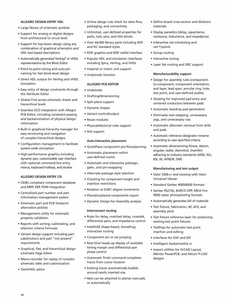
Allegro PCB Editor makes it easy to generateany type of manufacturing output you need
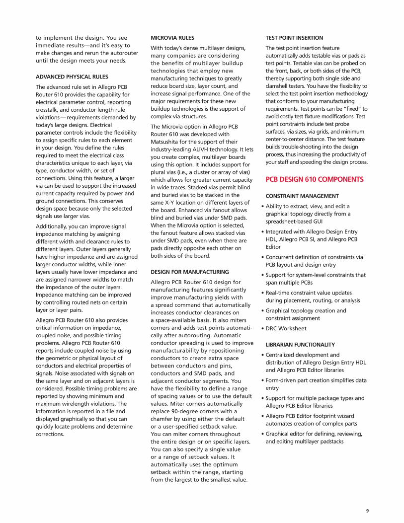
Extensive manufacturability checkingprevents slivers, shorts, orunmanufacturable copper islands
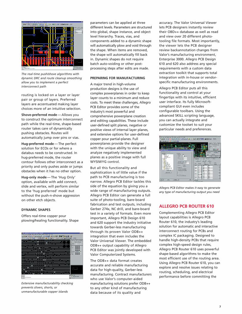
The real-time push/shove algorithms withdynamic DRC and route cleanup smoothingallow you to implement a perfectinterconnect path

8
design to manufacturing. The resultsare increased productivity andshortened design cycles.
With Allegro PCB Router 610, PCBdesigners can investigate repeatablerouting strategies and determine theeffect on delay, crosstalk, impedancecontrol, differential pairs, and netscheduling. Comprehensive capabilitiesin Allegro PCB Router 610 includecontrollable true 45-degree routingthat can be used on all nets, or justused for orthogonal corner mitering,auto net-shielding with auto via-stitching, and full Microvia structuresupport. Allegro PCB Router 610 makesthe most efficient use of the PCB routingarea, resulting in high completion rateson PCBs with complex designs.
SEAMLESS INTEGRATION WITHALLEGRO PCB EDITOR
Allegro PCB Router 610 is tightlycoupled with Allegro PCB Editor,providing a rapid translation-freepath for design autorouting. Allrouter setup is performed directlyinside Allegro PCB Editor using a
router setup wizard. The interfacethen takes the defined routingstrategy and all the design rules(both manufacturability and high-speed topology-based constraints)and executes the router in a batchmode. The router’s progress can betracked interactively from withinAllegro PCB Editor. Once the routingstrategy is completed, the routedinterconnect is automatically importedback into Allegro PCB Editor. Routingcan be performed on a single net, agroup of nets, or the whole design,allowing for the maximum in designflexibility.
HIGH-SPEED, RULES-DRIVEN ROUTING
Allegro PCB Router 610 reducescrosstalk by evaluating the geometricor physical layout of conductors andthe electrical properties of signalscarried by the conductors. Noiseassociated with conductors both onthe same layer and adjacent layers isconsidered. It controls cumulative noisecrosstalk by coupled noise rules thatincorporate the design’s electrical
properties. Allegro PCB Router 610dynamically computes the maximumcumulative crosstalk noise duringrouting. This is computed by summingall parallel and tandem conductors.The fast circuit features with PCBAllegro Router 610 can meet thetiming, crosstalk, and special geometryrequirements of today’s high-speedcircuits.
DIFFERENTIAL PAIRS, SHIELDED NETS,AND AREA RULES
Allegro PCB Router 610 also hasthe flexibility to handle the specialgeometry requirements of high-performance designs. For differentialpair routing, you define the gapbetween the two conductors andthe autorouter takes care of the rest.Allegro PCB Router 610 intelligentlyhandles routing around or throughvias and automatically conforms toany defined minimum length criteria.Turbo Stagger technology optimizesdesigns where large numbers ofdifferential pairs exist and wheremany of the designs’ componentsinclude staggered pin arrays. Usingthe optional Turbo Stagger featureon such designs can boost routerperformance by as much as 300%.
Automatic net shielding is used toreduce noise on noise-sensitive nets.Separate design rules may be appliedto different regions of the design.For example, you can specify tightclearance rules in the connector areaof your design and less stringent rulesin the rest of your design.
With signal margins shrinking rapidly,the use of net shielding is becomingcommonplace on most high-speeddesigns. In order for net shielding toperform correctly, the shields needto be connected to the groundplaneat regular intervals so that any straynoise can be effectively absorbed.Allegro PCB Router 610 not only auto-generates the shield around specifiednets, but also it automatically ties theshield route to the chosen groundplaneby automatically inserting vias atspecified distances. As a designer,you define design rules such as gapsbetween conductors and minimumlength criteria and use the autorouterDifferential signaling is automatically
managed within the PCB Router duringautorouting to a defined separation spacing
Shielded signal routing automaticallycreates the signal — a shield pair withpre-defined tap vias to a groundplane
The PCB Router provides the PCB designerwith a powerful graphical environment forauto/interactive shape-based floorplanningand routing
Seamless integration of the PCB Routerwith the PCB Editor creates a total PCBdesign environment — wizards make setup,control, monitoring, and driving theautorouter simple
9
to implement the design. You seeimmediate results—and it’s easy tomake changes and rerun the autorouteruntil the design meets your needs.
ADVANCED PHYSICAL RULES
The advanced rule set in Allegro PCBRouter 610 provides the capability forelectrical parameter control, reportingcrosstalk, and conductor length ruleviolations—requirements demanded bytoday’s large designs. Electricalparameter controls include the flexibilityto assign specific rules to each elementin your design. You define the rulesrequired to meet the electrical classcharacteristics unique to each layer, viatype, conductor width, or set ofconnections. Using this feature, a largervia can be used to support the increasedcurrent capacity required by power andground connections. This conservesdesign space because only the selectedsignals use larger vias.
Additionally, you can improve signalimpedance matching by assigningdifferent width and clearance rules todifferent layers. Outer layers generallyhave higher impedance and are assignedlarger conductor widths, while innerlayers usually have lower impedance andare assigned narrower widths to matchthe impedance of the outer layers.Impedance matching can be improvedby controlling routed nets on certainlayer or layer pairs.
Allegro PCB Router 610 also providescritical information on impedance,coupled noise, and possible timingproblems. Allegro PCB Router 610reports include coupled noise by usingthe geometric or physical layout ofconductors and electrical properties ofsignals. Noise associated with signals onthe same layer and on adjacent layers isconsidered. Possible timing problems arereported by showing minimum andmaximum wirelength violations. Theinformation is reported in a file anddisplayed graphically so that you canquickly locate problems and determinecorrections.
MICROVIA RULES
With today’s dense multilayer designs,many companies are consideringthe benefits of multilayer builduptechnologies that employ newmanufacturing techniques to greatlyreduce board size, layer count, andincrease signal performance. One of themajor requirements for these newbuildup technologies is the support ofcomplex via structures.
The Microvia option in Allegro PCBRouter 610 was developed withMatsushita for the support of theirindustry-leading ALIVH technology. It letsyou create complex, multilayer boardsusing this option. It includes support forplural vias (i.e., a cluster or array of vias)which allows for greater current capacityin wide traces. Stacked vias permit blindand buried vias to be stacked in thesame X-Y location on different layers ofthe board. Enhanced via fanout allowsblind and buried vias under SMD pads.When the Microvia option is selected,the fanout feature allows stacked viasunder SMD pads, even when there arepads directly opposite each other onboth sides of the board.
DESIGN FOR MANUFACTURING
Allegro PCB Router 610 design formanufacturing features significantlyimprove manufacturing yields witha spread command that automaticallyincreases conductor clearances ona space-available basis. It also miterscorners and adds test points automati-cally after autorouting. Automaticconductor spreading is used to improvemanufacturability by repositioningconductors to create extra spacebetween conductors and pins,conductors and SMD pads, andadjacent conductor segments. Youhave the flexibility to define a rangeof spacing values or to use the defaultvalues. Miter corners automaticallyreplace 90-degree corners with achamfer by using either the defaultor a user-specified setback value.You can miter corners throughoutthe entire design or on specific layers.You can also specify a single valueor a range of setback values. Itautomatically uses the optimumsetback within the range, startingfrom the largest to the smallest value.
TEST POINT INSERTION
The test point insertion featureautomatically adds testable vias or pads astest points. Testable vias can be probed onthe front, back, or both sides of the PCB,thereby supporting both single side andclamshell testers. You have the flexibility toselect the test point insertion methodologythat conforms to your manufacturingrequirements. Test points can be “fixed” toavoid costly test fixture modifications. Testpoint constraints include test probesurfaces, via sizes, via grids, and minimumcenter-to-center distance. The test featurebuilds trouble-shooting into the designprocess, thus increasing the productivity ofyour staff and speeding the design process.
PCB DESIGN 610 COMPONENTS
CONSTRAINT MANAGEMENT
• Ability to extract, view, and edit agraphical topology directly from aspreadsheet-based GUI
• Integrated with Allegro Design EntryHDL, Allegro PCB SI, and Allegro PCBEditor
• Concurrent definition of constraints viaPCB layout and design entry
• Support for system-level constraints thatspan multiple PCBs
• Real-time constraint value updatesduring placement, routing, or analysis
• Graphical topology creation andconstraint assignment
• DRC Worksheet
LIBRARIAN FUNCTIONALITY
• Centralized development anddistribution of Allegro Design Entry HDLand Allegro PCB Editor libraries
• Form-driven part creation simplifies dataentry
• Support for multiple package types andAllegro PCB Editor libraries
• Allegro PCB Editor footprint wizardautomates creation of complex parts
• Graphical editor for defining, reviewing,and editing multilayer padstacks
10
ALLEGRO DESIGN ENTRY HDL
• Large library of schematic symbols
• Support for analog or digital designsfrom architectural to circuit level
• Support for top-down design using anycombination of graphical schematics andHDL text-based descriptions
• Automatically generated Verilog® or VHDLrepresentations by the Block Editor
• Point-to-point wiring and auto-pinnaming for fast block-level design
• Direct HDL output for Verilog and VHDLsimulation
• Easy entry of design constraints throughthe Attribute Editor
• Global Find across schematic sheets andhierarchical levels
• Seamless ECO integration with AllegroPCB Editor, including constraint-passingand backannotation of physical designinformation
• Built-in graphical hierarchy manager foreasy structuring and navigationof complex hierarchical designs
• Configuration management to facilitatesystem-wide simulation
• High-performance graphics includingdynamic pan, customizable user interfacewith optional command-line entry,menus, keyboard hotkeys, and strokes
ALLEGRO DESIGN ENTRY CIS
• ODBC-compliant component databaseand MRP, ERP, PDM integration
• Centralized part number and partinformation management system
• Schematic part and PCB footprintalternative picklists
• Management utility for schematicproperty validation
• Reports with sorting, subtotaling, andselection criteria formulas
• Variant design support including partsubstitutions and part “not present”requirements
• Graphical, flat, and hierarchical designschematic Page Editor
• Macro-recorder for replay of complexschematic edits and customization
• Text/VHDL editor
• Online design rule check for data flow,packaging, and connectivity
• Unlimited, user-defined properties forparts, nets, pins, and title blocks
• Over 44,000 library parts including IEEEand IEC standard styles
• EDIF graphics and EDIF netlist interface
• Popular HDL and simulation interfacesincluding Spice, Verilog, and VHDL
• Imperial or metric unit support
• Undo/redo function
ALLEGRO PCB EDITOR
• Undo/redo
• Drafting/dimensioning
• Split plane support
• Dynamic shapes
• Variant control/output
• Reuse modules
• Physical/electrical rules support
• Slot support
Auto-interactive placement
• QuickPlace component pre-floorplanning
• Automatic placement withinuser-defined rooms
• Automatic and interactive package-,gate-, and pin-swapping
• Alternate package style selection
• Checking for component height andinsertion restrictions
• Rotation at 0.001 degree increments
• Placed/unplaced components report
• Dynamic Design-for-Assembly analysis
Interconnect routing
• Rules for delay, matched delay, crosstalk,differential pairs, and impedance control
• IntelliUSE shape-based, shove/huginteractive routing
• Component pin or via jumping
• Real-time heads-up display of availabletiming margin and differential pairphase control
• Automatic finish command completestraces from cursor location
• Existing traces automatically bubblearound newly inserted vias
• Nets can be attached to planes manuallyor automatically
• Define board cross-section and dielectricmaterials
• Display parasitics (delay, capacitance,resistance, inductance, and impedance)
• Interactive net scheduling andnet T-points
• Group routing
• Interactive tuning
• Layer Set routing and DRC support
Manufacturability support
• Design for assembly rules (component-to-component, component orientation,and layer, lead span, annular ring, hole,test point, and user-defined audits)
• Glossing for improved pad entry andcentered conductors between pads
• Automatic teardrop pad generation
• Eliminates stair-stepping, unnecessaryjogs, and unnecessary vias
• Automatic silkscreen removal from drillsand pads
• Automatic reference designator renameaccording to user-specified criteria
• Automatic dimensioning (linear, datum,angular, radial, diametral, chamfer)adhering to industry standards (ANSI, ISO,BSI, JIS, AFNOR, DIN)
Manufacturing and test output
• Valor ODB++ and viewing with ValorUniversal Viewer
• Standard Gerber 4000/6000 formats
• Gerber RS274x, BARCO DPF, MDA Fire9000 raster photoplotting formats
• Automatically generates bill of materials
• Test fixture, fabrication, NC drill, andassembly plots
• Test fixture reference layer for preservingexisting test point fixtures
• TestPrep for automatic test pointinsertion and editing
• Interfaces for DXF and IDF
• Intelligent Gerber/netlist in
• Import utilities for OrCAD Layout,Mentor PowerPCB, and Altium P-CADdesigns
11
ALLEGRO PCB ROUTER 610
True shape-based routing
• Shape-based or grid-based autorouting
• Concurrent routing of up to 256signal layers
• SMD fanout to vias
• 45-degree routing
• Bus routing (SMD or through-hole)
• Via rules by net, net class
• Wire and clearance rules by layer
• Net/net class rules by layer
• Soft and hard fences
• Automatic wire spreading and test pointgeneration
• Blind and buried vias
• Vias under SMD pads
• Plural vias
• Automatic wirebonding
• Automatic gate- and pin-swappingduring routing
• Parallelism control
• Accumulative noise control
• Maximum/minimum/matchedlength control
• Automatic differential pair routing withTurbo Stagger technology
• Rules/clearance by area
• Net shielding
• Virtual pins for complex topologies
• Layer set routing
Route Editor
• Ghosting, shoving, and plowing
• Interactive via search
• Online design rule checking
• Automatic routing cleanup
• Online meter displays length tolerance
• Global violation indicator
• Dynamically calculates and displaysavailable timing slack
• Color feedback on all indicatorsand meters
• Multiple net (bus bundle) routing
• Single net autorouting
Placement Editor
• Online design rule checking
• Floorplanning
• Guided placement mode
• Flip, rotate, align, push, and moveindividual components or groupsof components
• Placement density analysis
• Direct X-Y location componentplacement
Autoplacement
• Automatic double-sided componentplacement
• Rules by layer, component, and/orcomponent type
• Automatic gate- and pin-swapping
• Auto-clustering
OPERATING SYSTEM SUPPORT• Red Hat Linux 7.3, 8.0, RHEL 3.0
• Windows 2000 with Service Pack 4,XP Professional
• Sun Solaris 8, 9
• HP-UX 11.0, 11.11i
• IBM AIX 5.1
CADENCE SERVICESAND SUPPORT
• Cadence application engineers cananswer your technical questions bytelephone, email, or Internet—they canalso provide technical assistance andcustom training
• Cadence certified instructors teach over70 courses and bring their real-worldexperience into the classroom
• Over 25 Internet Learning Series (iLS)online Courses allow you the flexibility oftraining at Your own computer via theInternet
• SourceLink® online customer supportgives you answers to your technicalquestions—24 hours a day, 7 days aweek—including the latest in quarterlysoftware rollups, product change releaseinformation, technical documentation,solutions, software updates, and more
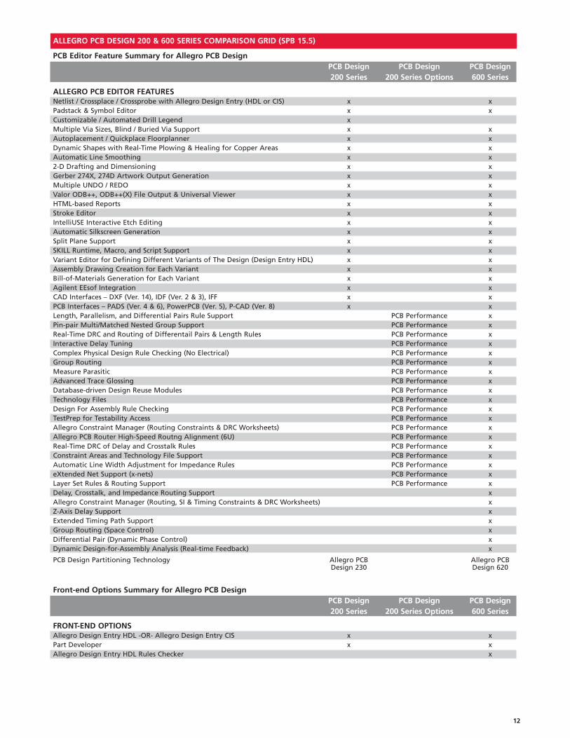
12
PCB Editor Feature Summary for Allegro PCB DesignPCB Design PCB Design PCB Design200 Series 200 Series Options 600 Series
ALLEGRO PCB EDITOR FEATURESNetlist / Crossplace / Crossprobe with Allegro Design Entry (HDL or CIS) x xPadstack & Symbol Editor x xCustomizable / Automated Drill Legend xMultiple Via Sizes, Blind / Buried Via Support x xAutoplacement / Quickplace Floorplanner x xDynamic Shapes with Real-Time Plowing & Healing for Copper Areas x xAutomatic Line Smoothing x x2-D Drafting and Dimensioning x xGerber 274X, 274D Artwork Output Generation x xMultiple UNDO / REDO x xValor ODB++, ODB++(X) File Output & Universal Viewer x xHTML-based Reports x xStroke Editor x xIntelliUSE Interactive Etch Editing x xAutomatic Silkscreen Generation x xSplit Plane Support x xSKILL Runtime, Macro, and Script Support x xVariant Editor for Defining Different Variants of The Design (Design Entry HDL) x xAssembly Drawing Creation for Each Variant x xBill-of-Materials Generation for Each Variant x xAgilent EEsof Integration x xCAD Interfaces – DXF (Ver. 14), IDF (Ver. 2 & 3), IFF x xPCB Interfaces – PADS (Ver. 4 & 6), PowerPCB (Ver. 5), P-CAD (Ver. 8) x xLength, Parallelism, and Differential Pairs Rule Support PCB Performance xPin-pair Multi/Matched Nested Group Support PCB Performance xReal-Time DRC and Routing of Differentail Pairs & Length Rules PCB Performance xInteractive Delay Tuning PCB Performance xComplex Physical Design Rule Checking (No Electrical) PCB Performance xGroup Routing PCB Performance xMeasure Parasitic PCB Performance xAdvanced Trace Glossing PCB Performance xDatabase-driven Design Reuse Modules PCB Performance xTechnology Files PCB Performance xDesign For Assembly Rule Checking PCB Performance xTestPrep for Testability Access PCB Performance xAllegro Constraint Manager (Routing Constraints & DRC Worksheets) PCB Performance xAllegro PCB Router High-Speed Routng Alignment (6U) PCB Performance xReal-Time DRC of Delay and Crosstalk Rules PCB Performance xConstraint Areas and Technology File Support PCB Performance xAutomatic Line Width Adjustment for Impedance Rules PCB Performance xeXtended Net Support (x-nets) PCB Performance xLayer Set Rules & Routing Support PCB Performance xDelay, Crosstalk, and Impedance Routing Support xAllegro Constraint Manager (Routing, SI & Timing Constraints & DRC Worksheets) xZ-Axis Delay Support xExtended Timing Path Support xGroup Routing (Space Control) xDifferential Pair (Dynamic Phase Control) xDynamic Design-for-Assembly Analysis (Real-time Feedback) x
PCB Design Partitioning Technology Allegro PCB Allegro PCBDesign 230 Design 620
Front-end Options Summary for Allegro PCB DesignPCB Design PCB Design PCB Design200 Series 200 Series Options 600 Series
FRONT-END OPTIONSAllegro Design Entry HDL -OR- Allegro Design Entry CIS x xPart Developer x xAllegro Design Entry HDL Rules Checker x
ALLEGRO PCB DESIGN 200 & 600 SERIES COMPARISON GRID (SPB 15.5)
© 2005 Cadence Design Systems, Inc. All rights reserved.Cadence, the Cadence logo, Allegro, OrCAD Layout,SourceLink, Verilog, and Virtuoso are registered trademarks,and Encounter is a trademark of Cadence Design Systems,Inc. P-CAD is a registered trademark of Altium Limited. Allothers are properties of their respective holders.
4431E 06/05
FOR MORE INFORMATIONContact Cadence sales at 1.800.746.6223or visit www.cadence.com foradditional information. To locate aCadence sales office or value-addedreseller (VAR) in your area, visitwww.cadence.com/contact_us.
F
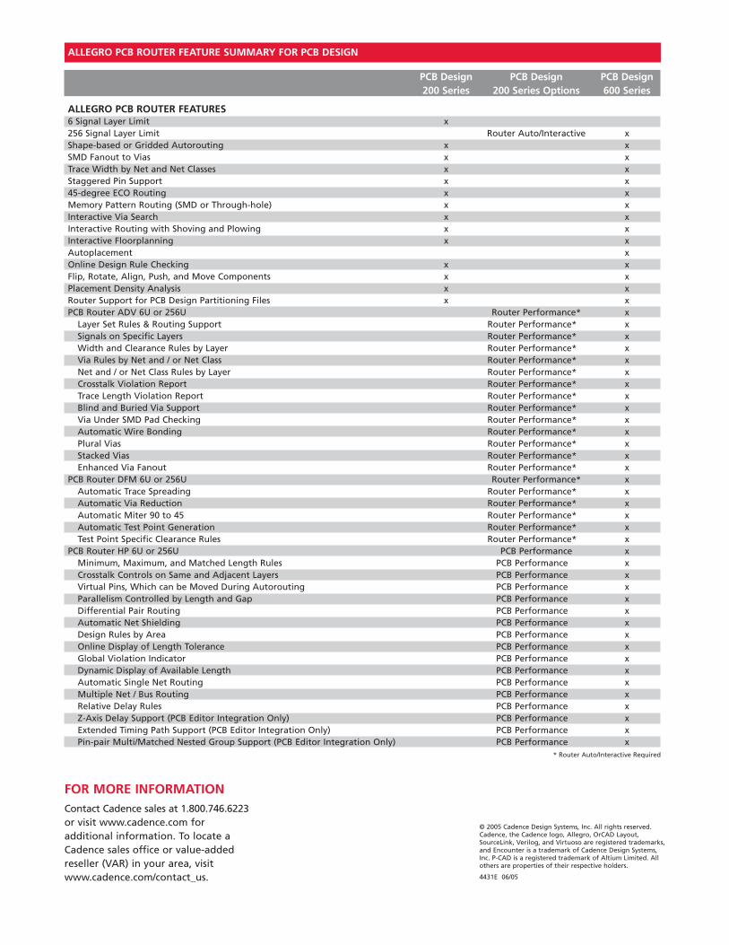
PCB Design PCB Design PCB Design200 Series 200 Series Options 600 Series
ALLEGRO PCB ROUTER FEATURES6 Signal Layer Limit x256 Signal Layer Limit Router Auto/Interactive xShape-based or Gridded Autorouting x xSMD Fanout to Vias x xTrace Width by Net and Net Classes x xStaggered Pin Support x x45-degree ECO Routing x xMemory Pattern Routing (SMD or Through-hole) x xInteractive Via Search x xInteractive Routing with Shoving and Plowing x xInteractive Floorplanning x xAutoplacement xOnline Design Rule Checking x xFlip, Rotate, Align, Push, and Move Components x xPlacement Density Analysis x xRouter Support for PCB Design Partitioning Files x xPCB Router ADV 6U or 256U Router Performance* x
Layer Set Rules & Routing Support Router Performance* xSignals on Specific Layers Router Performance* xWidth and Clearance Rules by Layer Router Performance* xVia Rules by Net and / or Net Class Router Performance* xNet and / or Net Class Rules by Layer Router Performance* xCrosstalk Violation Report Router Performance* xTrace Length Violation Report Router Performance* xBlind and Buried Via Support Router Performance* xVia Under SMD Pad Checking Router Performance* xAutomatic Wire Bonding Router Performance* xPlural Vias Router Performance* xStacked Vias Router Performance* xEnhanced Via Fanout Router Performance* x
PCB Router DFM 6U or 256U Router Performance* xAutomatic Trace Spreading Router Performance* xAutomatic Via Reduction Router Performance* xAutomatic Miter 90 to 45 Router Performance* xAutomatic Test Point Generation Router Performance* xTest Point Specific Clearance Rules Router Performance* x
PCB Router HP 6U or 256U PCB Performance xMinimum, Maximum, and Matched Length Rules PCB Performance xCrosstalk Controls on Same and Adjacent Layers PCB Performance xVirtual Pins, Which can be Moved During Autorouting PCB Performance xParallelism Controlled by Length and Gap PCB Performance xDifferential Pair Routing PCB Performance xAutomatic Net Shielding PCB Performance xDesign Rules by Area PCB Performance xOnline Display of Length Tolerance PCB Performance xGlobal Violation Indicator PCB Performance xDynamic Display of Available Length PCB Performance xAutomatic Single Net Routing PCB Performance xMultiple Net / Bus Routing PCB Performance xRelative Delay Rules PCB Performance xZ-Axis Delay Support (PCB Editor Integration Only) PCB Performance xExtended Timing Path Support (PCB Editor Integration Only) PCB Performance xPin-pair Multi/Matched Nested Group Support (PCB Editor Integration Only) PCB Performance x
* Router Auto/Interactive Required
ALLEGRO PCB ROUTER FEATURE SUMMARY FOR PCB DESIGN