all-optical ultrasound transducers for high resolution
TRANSCRIPT

All-Optical Ultrasound Transducers for High Resolution Imaging
A Thesis SUBMITTED TO THE FACULTY OF
UNIVERSITY OF MINNESOTA BY
Clay Smith Sheaff
IN PARTIAL FULFILLMENT OF THE REQUIREMENTS FOR THE DEGREE OF
DOCTOR OF PHILOSOPHY
Shai Ashkenazi, Adviser
December 2014

© Clay Smith Sheaff 2014

i
Acknowledgements
I would like to begin by expressing my gratitude to Dr. Shai Ashkenazi for taking me on
as his first student. Prior to our meeting, I had little idea of what path was right for me. At
the last second of my visit to UMN, we had an impromptu chat about his research. It
struck such a chord that afterwards I felt a security not experienced in years. Had that
meeting not occurred or had I not been so accepted, I cannot imagine that the past six
years would have been much less tumultuous than the previous three. I would also like
to thank Dr. Ashkenazi for his patience, insight, and guidance during my time here at
UMN. I consider the general problem-solving skills adopted as his understudy to be the
most valuable asset attained in my graduate school career. Most importantly, I thank him
for his genuine interest in the well-being of his students. It is easily assumed that a
cordial and accomplished adviser is necessarily a supportive one. I consider myself
lucky to have been advised by someone who is truly all three.
Secondly, I would like to thank my committee members, past and present, for their time
in reviewing my work. They include Dr. Taner Akkin, Dr. Emad Ebbini, Dr. David Hunter,
and Dr. James Leger.
Departmental and technical staff have been immeasurably helpful. I thank Rachel
Jorgenson for her general advisement and her cheerful and reliable assistance with all
things bureaucratic. I have also appreciated the staff of the Minnesota Nano Center,
particularly Lage von Dissen, who never fails to be interested and helpful.
The support of friends gained along the way has been invaluable. To my comrades
Ekaterina Morgounova and Mohammad Amin Tadayon, you have my gratitude for your
assistance both inside and outside of the lab. From proofreaders to mock therapists, I
would not have been as published or even-tempered without you. I cannot begin to
thank Daisy Cross and her husband Nathan Lockwood for offering friendship that I will
always hold dear. When it comes to tolerating bitterly cold winters, their inviting home
has made the difference.

ii
To my family, I thank my Aunt and Uncle Sinclair for always keeping their door open to
me. They provided the slice of home that at times I so desperately needed. To my
sisters Kim and Kelly, thank you for making such squeezable little rug rats whom have
consistently brightened my return to the heartland. And certainly most of all, I thank my
parents. I am confident that I would not have made it this far without the drive instilled in
me by my father and the loving care so unwaveringly provided by my mother. Any
virtues that I possess, I owe to them both.
Lastly, I extend a handshake to myself. Congratulations sir. Given the circumstances,
you have done the impossible. You know of what I speak and always will.
.

iii
Table of Contents
Acknowledgments i
Table of Contents iii
List of Figures vi
List of Tables iv
List of Abbreviations x
Chapter 1 - Introduction 1
1.1 Clinical Significant of High Frequency Ultrasound………………………………………………...1
1.2 Endoscopic Transducer Arrays………………………………………………………...…………... 2
1.3 Optical Ultrasound Transduction…………………………………………………………………… 4
1.3.1 Etalon Receivers……………………………………………………………………………….. 4
1.3.1.1 Introduction……………………………………………………………………………….. 4
1.3.1.2 Theoretical Model of Etalon Detection…………………………………………………. 6
1.3.2 Integrated All-optical Transducers…….……………………………………………………... 9
1.3.2.1 Introduction……………………………………………………………………………….. 9
1.3.2.2 Previous Designs for All-optical Transducers………….……………………………... 9
1.3.2.3 PI-etalon for All-optical Ultrasound Transduction…………………………………… 10
1.3.2.4 Theoretical Model of TUG in Optically Thick Films…………………………………. 12
1.4 Statement of Objectives and Overview of this Thesis………………………………………….. 14
Chapter 2 – Fabrication and Characterization of Waf er-based PI-etalons 16
2.1 Overview…..………………………………………………………………………………………… 16
2.2 Introduction………………………………………………………………………………………….. 16
2.3 Methods and Results………………………………………………………………………………. 17
2.3.1 Characterization of PI-2555/2525……………………………………………………………17

iv
2.3.1.1 Optical Absorbance and Penetration Depth…………………………………………. 17
2.3.1.2 TUG in Solitary PI films………………………………………………………………… 19
2.3.2 Transducer Fabrication………………………………………………………………………. 22
2.3.3 Transducer Characterization………………………………………………………………… 24
2.3.3.1 Optical Resonance………………………………………………………………………24
2.3.3.2 Acoustic Performance………………………………………………………………….. 26
2.3.3.2a Receive Sensitivity and Bandwidth……………………………………………… 26
2.3.3.2b TUG Amplitude and Spectrums…...……………………………………………...29
2.3.3.2c Directivity…………………………………………………………………………… 31
2.3.3.2d Pulse-echo…………………………………………………………………………. 34
2.3.3.2e Damage Threshold and Maximum Pressure…………………………………… 37
2.4 Discussion……………………………………………………………………………………………39
Chapter 3 – Imaging with Wafer-based PI-etalon 42
3.1 Overview…..………………………………………………………………………………………… 42
3.2 Introduction………………………………………………………………………………………….. 42
3.3 Methods and Results………………………………………………………………………………. 45
3.3.1 Imaging with Fixed-transmitter/Scanning-receiver………………………………………... 45
3.3.1.1 Scan Methods and Data Acquisition………………………………………………….. 45
3.3.1.2 Post-processing and Image Reconstruction………………………………………….48
3.3.1.3 Ex vivo Imaging of Carotid Artery in Swine………………………………………….. 52
3.3.2 Imaging with Fixed-receiver/Scanning-transmitter………………………………………... 53
3.3.2.1 Scan Methods and Data Acquisition………………………………………………….. 53
3.3.2.2 Post-processing and Image Reconstruction………………………………………….58
3.4 Discussion…………………………………………………………………………………………… 62
Chapter 4 – Fiber Optic Etalon for PAI 67
4.1 Overview…..………………………………………………………………………………………… 67
4.2 Introduction………………………………………………………………………………………….. 67
4.2.1 Angiogenesis………………………………………………………………………………….. 68
4.2.2 Hypoxia………………………………………………………………………………………… 68
4.2.3 Photoacoustic Endoscopy…………………………………………………………………… 69
4.3 Methods and Results………………………………………………………………………………. 70
4.3.1 Fabrication…………………………………………………………………………………….. 70
4.3.2 Characterization………………………………………………………………………………. 71

v
4.3.2.1 Optical Resonance………………………………………………………………………71
4.3.2.2 Acoustic Performance………………………………………………………………….. 72
4.3.3 PAI with a Synthetic Aperture……………………………………………………………….. 75
4.4 Discussion…………………………………………………………………………………………..77
Chapter 5 - Towards a Fiber Optic PI-etalon Imager 80
5.1 Overview..…………………………………………………………………………………………… 80
5.2 Introduction………………………………………………………………………………………….. 80
5.3 Methods and Results………………………………………………………………………………. 81
5.3.1 Fiber Selection and Characterization………………………………………………………. 81
5.3.2 Fabrication…………………………………………………………………………………….. 84
5.3.2.1 Introduction……………………………………………………………………………… 84
5.3.2.2 PI Deposition on Optical Fibers……………………………………………………….. 84
5.3.2.3 Fabrication of Etalon Layers……………………………………………………………87
5.3.3 Supporting Optics…………………………………………………………………………….. 87
5.3.3.1 Optical Circulation………………………………………………………………………. 87
5.3.3.2 Selection of Focusing Lens……………………………………………………………. 90
5.3.4 Device Characterization……………………………………………………………………… 90
5.3.4.1 Acoustic Transmission…………………………………………………………………. 90
5.3.4.2 Etalon Reception………………………………………………………………………...90
5.4 Discussion…………………………………………………………………………………………… 91
Chapter 6 – Summary and Future Directions 92
6.1 Summary…………………………………………………………………………………………….. 92
6.2 Future Directions…………………………………………………………………………………….94
6.2.1 Near-term Goals……………………………………………………………………………….94
6.2.2 Lateral Beam Confinement………………………………………………………………….. 94
6.2.3 Alternatives to Synthetic Apertures…………………………………………………………. 97
6.2.4 Dual-mode Pulse-echo/PAI………………………………………………………………… 101
Bibliography 103

vi
List of Figures Chapter 1 – Introduction 1
Figure 1.1. Side-looking IVUS using single-element rotation and cylindrical array……………….... 3
Figure 1.2. Designs for forward-looking IVUS imagers…………………………………………………4
Figure 1.3. Mechanism for optical detection of ultrasound with a thin film etalon…………………... 5
Figure 1.4. Theoretical resonance curves for two etalons of different optical finesse……………… 7
Figure 1.5. Previous designs for an all-optical ultrasound transducer ……..………………………. 10
Figure 1.6. Beam-scanning technique for imaging with device in Figure 1.5b…………………….. 11
Figure 1.7. Design concept for a PI-etalon all-optical ultrasound transducer……………………… 11
Figure 1.8. Pressure impulse response for TUG in a 10 µm polymer film…………………………. 15
Chapter 2 - Fabrication and Characterization of Waf er-based PI-etalons 16
Figure 2.1. Absorbance spectrum for PI-2555/2525………………………………………………….. 18
Figure 2.2. Photograph of PI samples of varying thickness with a CCD image of illumination….. 20
Figure 2.3. Average pressure generated in PI films of eight different thicknesses………………...21
Figure 2.4. Illustration of PI-etalon structure for Au/Au and Die/Au designs………………………. 22
Figure 2.5. Transmittance spectrum of dielectric mirror used in Die/Au PI-etalon………………… 24
Figure 2.6. Optical and DAQ system for acquiring resonance curve……………………………….. 25
Figure 2.7. Optical resonance profile for Au/Au and Die/Au etalon designs……………………….. 26
Figure 2.8. Pulse-echo of 25 MHz probe and detection of pulse by Au/Au etalon…………………27
Figure 2.9. Optical and DAQ system for detection of 25 MHz probe with etalon………………….. 28
Figure 2.10. Optical and DAQ setup for detecting TUG resulting from absorption of UV pulse.....30
Figure 2.11. Example waveforms of acoustic emission for Au/Au and Die/Au designs…………...31
Figure 2.12. Optomechanical system for detecting transmit directivity……………………………...32
Figure 2.13. Broadband directivity profiles for 43 µm UV spot with Die/Au and Au/Au design…...33
Figure 2.14. Graphic for estimating effective radius of an etalon element……………………….....35
Figure 2.15. Optical and DAQ system for pulse-echo measurements……………………………… 36
Figure 2.16. Etalon signal corresponding to thermoelastic expansion of its cavity……………….. 37
Figure 2.17. Example pulse-echo waveforms for Au/Au and Die/Au designs……………………... 38

vii
Chapter 3 - Imaging with Wafer-based PI-etalon 42
Figure 3.1. Optical and DAQ system for fixed-transmitter/scanning-receiver imaging………….... 46
Figure 3.2. Photograph of experimental setup for fixed-transmitter/scanning-receiver imaging… 46
Figure 3.3. Pulse-echo waveform and spectrum for Au/Au Pi-etalon with Continuum laser…….. 47
Figure 3.4. Drift of single resonance over 1 mm at 100 µm step size for Au/Au device………….. 48
Figure 3.5. Acoustic propagation model for fixed-transmitter/scanning-receiver image recon…... 50
Figure 3.6. Image reconstruction of two 80 µm wires………………………………………………… 50
Figure 3.7. 1-D slices of 3-D reconstruction for resolution estimation……………………………… 51
Figure 3.8. Photograph and reconstruction of an excised coronary artery from swine…………… 52
Figure 3.9. Optical and DAQ system for fixed-receiver/scanning-transmitter imaging………….... 54
Figure 3.10. Photograph of optical system for fixed-receiver/scanning-transmitter imaging……...54
Figure 3.11. Scan pattern intended for fixed-receiver/scanning-transmitter imaging……………...55
Figure 3.12. Beam position adjustments required to maintain same transmit grid coordinates…. 56
Figure 3.13. Receive array used for imaging as determined by acoustic trilateration……………..58
Figure 3.14. Propagation model for fixed-receiver/scanning-transmitter image reconstruction… 59
Figure 3.15. Image reconstruction of two 127 µm wires……………………………………………... 60
Figure 3.16. Comparison between two receivers of 2-D reconstructions…………………………...61
Figure 3.17. Propagation of thermoelastic waveform in etalon later………………………………... 62
Figure 3.18. Different scan lens types to consider for achieving orthogonal grids…………………65
Chapter 4 - Fiber Optic Etalon for PAI 67
Figure 4.1. Optical and DAQ system for resonance measurement of fiber optic etalon………….. 71
Figure 4.2. Normalized resonance profile of fiber optic etalon…………………………………….... 72
Figure 4.3. Optical and DAQ system for evaluating sensitivity and spectrum of fiber etalon……..73
Figure 4.4. TUG waveform detected by fiber etalon and spectrum……………………………….... 74
Figure 4.5. Pulse-echo of 25 MHz probe and the waveform detected by fiber etalon……………. 75
Figure 4.6. Optical and DAQ system for synthetic aperture imaging of photoacoustic target…… 76
Figure 4.7. Orthogonal 2-D reconstructions of 50 µm polystyrene bead……………………...….... 76
Figure 4.8. Orthogonal 2-D reconstructions of 60 µm hair……………………………….………….. 77
Figure 4.9. Fiber optic system for fiber etalon array………………………………………………….. 78
Chapter 5 - Towards a Fiber Optic PI-etalon Imager 80
Figure 5.1. Image transmission through an image bundle and non-coherent bundle…………......82
Figure 5.2. Attenuation spectrum of Ceramoptec Optran WF fiber……………………………….....83

viii
Figure 5.3. Photograph of 7-element bundle and vertical profile of bundle surface…………….....83
Figure 5.4. General thin film structure for PI-etalon…………………………………………………... 84
Figure 5.5. Setup for spray coating of PI using an airbrush…………………………………………. 85
Figure 5.6. Photograph of fiber spray-coated with PI-2555 and transmitted pressure waveform.. 87
Figure 5.7. Ideal optical system for fiber optic-based PI-etalon imager……………………………..88
Figure 5.8. Proposed optical system for supporting a fiber optic PI-etalon array………………… 89
Chapter 6 - Summary and Future Directions 92
Figure 6.1. Illustration of laser light propagation into a flat and concave etalon cavity…………… 95
Figure 6.2. Fabrication process for polymer waveguide etalon……………………………………. 96
Figure 6.3. Proposed optical system for fixed-receiver/scanning-transmitter imaging………….... 98
Figure 6.4. Multi-channel, parallel-acquisition detection of ultrasound with an etalon…………... 99
Figure 6.5. Focusing of optically-generated ultrasound using a Fresnel zone plate…………….. 100
Figure 6.6. Concept for an all fiber optic imaging system of a fiber PI-etalon array……………...101
Figure 6.7. Potential optical system for dual-mode pulse-echo/PAI using PI-etalon array………102

ix
List of Tables
Chapter 1 – Introduction 1
Table 1.1 Comparison of device parameters for three different etalons…………………………….8
Table 1.2 Material properties for metals and polymers found in optical transducers……………. 12
Chapter 2 - Fabrication and Characterization of Waf er-based PI-etalons 16
Table 2.1 Comparison of performance parameters between Die/Au and Au/Au PI-etalons…….40

x
List of Abbreviations
Au Gold
Au/Au PI-etalon with PI/Au/SU-8/Au layers
BS Beam Splitter
CCD Charged-coupled device
CMUT Capacitive Micromachined Ultrasound Transducer
CT Computed Tomography
CW Continuous Wave
DAQ Data Acquisition
Die Dielectric
Die/Au PI-etalon with PI/Die/PI/Au layers
FIR Finite Impulse Response
FOC Fiber Optic Circulator
FPS Frames Per Second
FSR Free Spectral Range
FWHM Full-width half-maximum
HFUS High Frequency Ultrasound
IVUS Intravascular Ultrasound
MEMS Micro-electro-mechanical Systems
MM Multi-mode
MRI Magnetic Resonance Imaging
NA Numerical Aperture
NEP Noise-equivalent Pressure
NIR Near-infrared
OS Optical Switch
PAI Photoacoustic Imaging
PAE Photoacoustic Endoscopy
PBS Polarizing Beam Splitter
PD Photodetector
PDMS Polydimethylsiloxane
PI Polyimide
PRF Pulse Repetition Frequency

xi
PXI PCI eXtensions for Instrumentation
SAFT Synthetic Aperture Focusing Technique
SM Single Mode
SNR Signal-to-Noise Ratio
TUG Thermoelastic Ultrasound Generation
UV Ultraviolet

1
Chapter 1
Introduction
1.1 Clinical Significance of High Frequency Ultraso und
Within the past few decades, high frequency ultrasound (HFUS) (> 20 MHz) has
increasingly been used to provide high resolution (< 200 µm) imaging in medical
applications such as endoluminal imaging, intravascular imaging, ophthalmology, and
dermatology. While clinical magnetic resonance imaging (MRI) and X-ray computed
tomography (CT) systems continue to approach these resolutions (3T MRI scanners ~
500 µm [1], CT ~ 400 µm [2]-[3]), their expense, safety, and bulkiness make them non-
ideal candidates for routine interventional procedures. Furthermore, their limited
temporal resolution – typically below a few frames per second (FPS) – inhibits the
effective imaging of moving structures, guidance of interventional therapies, and rapid
diagnosis of disease. The majority of ultrasound imaging systems are both portable and
safe (no ionizing radiation), and they produce frame rates exceeding 25 FPS – the
approximate threshold for real-time operation. Optical Coherence Tomography (OCT)
can also provide real-time imaging and with better spatial resolution (< 10 µm) than
ultrasound, however HFUS allows for larger penetration depth (~ 10 mm) and hence a
larger field of view than OCT (< 1 mm). Photoacoustic imaging (PAI) has also derived
from ultrasound technology – a modality wherein tissue is irradiated with high energy
laser pulses to produce HFUS. This method combines the penetration depth of
ultrasound with optical absorption contrast to differentiate between tissue types and map
metabolic activity.
Due to the relatively limited field-of-view, clinical HFUS applications are either superficial
or endoscopic. In the imaging of superficial structures, a single transducer is typically
scanned across a linear or arced path that is parallel with the sample. Ultrasound
Biomicroscopy (UBM) is the most notable example – a modality that can image the
anterior structures of the eye in order to assess trauma, melanomas, glaucoma, and
other ocular diseases [4]. Commercial UBM systems operate as high as 50 MHz (Optos

2
OTI-Scan 3000, Quantel Medical Aviso), but an experimental system using a 200 MHz
transducer has been demonstrated [5]. Systems similar to those of UBM have been
used to image pathologies of the skin, but only in a research environment. Examples of
clinical studies include measuring the thickness of the dermis, examining cutaneous
lesions, and assessing the depth and margins of skin tumors [4].
The spatial constraints imposed by lumens and arteries in endoscopic applications make
the scanning of a single transducer across a linear path very difficult. Rotation of an
outward facing transducer, or radial scanning, is therefore typically employed.
Applications include searching for lesions in the wall layers of the gastrointestinal (GI)
tract as well as the biliary/pancreatic ducts, with commercial devices operating as high
as 25-30 MHz (Fujifilm P2625-M, Olympus UM-S30-20R). A modality under wide-spread
investigation is side-viewing intravascular ultrasound (IVUS), which is used to observe
the extent and composition of atherosclerotic plaque buildup in coronary and peripheral
arteries. Commercial IVUS systems operate as high as 40-45 MHz (Volcano
Revolutions, Boston Scientific Atlantis SR Pro), and experimental devices functioning as
high as 80 MHz have been reported [6], [7]. In order to look in front of the catheter as
opposed to the side, radially-scanning IVUS probes have been modified such that a
conical mirror deflects the acoustic emission in the forward direction [8]. Known as
forward-viewing/looking IVUS, this modality would allow characterization of occlusions
without the need for penetration, which can restrict blood flow and increase the risk for
ischemia. Forward-facing transducers have also been implemented for this purpose,
relying on the rocking/tilting of a single element to perform a sector scan [9].
1.2 Endoscopic Transducer Arrays
The disadvantages of scanning a single element in an endoscopic environment include a
fixed focus and the inability to employ beam-forming. As a result, there is a non-uniform
depth of field with limited circumferential resolution in the case of radial scanning and
limited lateral resolution when looking forward (> 200 µm). Furthermore, the inclusion of
moving parts presents fabrication difficulties, adds bulk, and reduces flexibility. In the
case of forwarding-facing transducers, this effectively disqualifies its use within the
coronary arteries where the identification of vulnerable plaque is the most critical. Finally,

mechanical scanning can introduce image artifacts due to the non
scanning mechanism. This results from the mechanical strain induced by the bending of
the device when inside the body [10].
The development of endoscopic phased arrays in o
shortcomings of scanned transducers is extensive and ongoing. Cylindrical phased
arrays have been employed as an alternative to radial scanning so as to eliminate the
rotational mechanism, thereby providing more uniform resolutio
focusing (Figure 1.1) [11]. A ubiquitous IVUS system using a cylindrical array is the
Volcano Eagle Eye, which consists of 64 line elements circumferentially distributed
about a 1.7 mm catheter, operating at 20 MHz.
been developed for forward
20 MHz, 1.4 mm array consisting of two concentric
micromachined ultrasound transducers (CMUT)
receiving (Figure 1.2a) [12]. Linear arrays making use of the entire face of the catheter
have also been developed, however the resultant gain in contrast comes at the expense
of frequency response; linear arrays small enough
10 MHz (Figure 1.2b) [13].
Figure 1.1 . Side-looking IVUS using phased array. A phased array avoids a rotational mechanism, provides beam forming, and allows a coaxial guidewire (Image by Boston Scientific).
3
ical scanning can introduce image artifacts due to the non-uniform velocity of the
scanning mechanism. This results from the mechanical strain induced by the bending of
the body [10].
The development of endoscopic phased arrays in order to compensate for the
shortcomings of scanned transducers is extensive and ongoing. Cylindrical phased
arrays have been employed as an alternative to radial scanning so as to eliminate the
rotational mechanism, thereby providing more uniform resolution through dynamic
) [11]. A ubiquitous IVUS system using a cylindrical array is the
Volcano Eagle Eye, which consists of 64 line elements circumferentially distributed
about a 1.7 mm catheter, operating at 20 MHz. Several array configurations have also
developed for forward-looking IVUS. The most promising development to date is a
20 MHz, 1.4 mm array consisting of two concentric ring arrays of capacitive
micromachined ultrasound transducers (CMUT) – one for transmitting and the other for
2a) [12]. Linear arrays making use of the entire face of the catheter
have also been developed, however the resultant gain in contrast comes at the expense
of frequency response; linear arrays small enough for IVUS applications rarely exceed
2b) [13].
looking IVUS using (a) single-element rotation and (b) sed array. A phased array avoids a rotational mechanism, provides beam
a coaxial guidewire (Image by Boston Scientific).
uniform velocity of the
scanning mechanism. This results from the mechanical strain induced by the bending of
rder to compensate for the
shortcomings of scanned transducers is extensive and ongoing. Cylindrical phased
arrays have been employed as an alternative to radial scanning so as to eliminate the
n through dynamic
) [11]. A ubiquitous IVUS system using a cylindrical array is the
Volcano Eagle Eye, which consists of 64 line elements circumferentially distributed
Several array configurations have also
looking IVUS. The most promising development to date is a
arrays of capacitive
ransmitting and the other for
2a) [12]. Linear arrays making use of the entire face of the catheter
have also been developed, however the resultant gain in contrast comes at the expense
for IVUS applications rarely exceed
a cylindrical sed array. A phased array avoids a rotational mechanism, provides beam

Despite the broad appeal of ultrasound imaging, there exists a disconnect between
commercial systems and high frequency operation. With respect to conventional
piezoelectric ceramics and composites, dice
transducers on the size s
become difficult to implement. The development of thin film polyvinylidene fluoride
(PVDF) and CMUTs has to some extent circumvented this problem, however these
devices are still susceptible to the s
devices. Such effects include a lowered electromechanical coupling factor, increased
noise due to small element capacitance, electrical crosstalk between channels, and RF
interference. This often necess
with circuitry, which ultimately limits the ability to implement dense arrays of HFUS
elements in a beam-forming capacity.
1.3 Optical Ultrasound Transduction
1.3.1 Etalon Receivers
1.3.1.1 Introduction
In concept, the optical detection and generation of HFUS using thin films offers
numerous advantages over traditional piezoelectric technology. Circumvention of an
Figure 1.2. Designs for forwardhollow center for a guidewire [12] (© 2014 IEEE) and with a mechanism for intracardiac RF ablation [13] (© 2008 IEEE).
4
broad appeal of ultrasound imaging, there exists a disconnect between
commercial systems and high frequency operation. With respect to conventional
piezoelectric ceramics and composites, dice-and-fill techniques used to fabricate
transducers on the size scale required for high frequency transduction (< 100 µm)
become difficult to implement. The development of thin film polyvinylidene fluoride
(PVDF) and CMUTs has to some extent circumvented this problem, however these
devices are still susceptible to the small scale effects found in traditional piezoelectric
devices. Such effects include a lowered electromechanical coupling factor, increased
noise due to small element capacitance, electrical crosstalk between channels, and RF
interference. This often necessitates front-end electronics in small probes already dense
with circuitry, which ultimately limits the ability to implement dense arrays of HFUS
forming capacity.
1.3 Optical Ultrasound Transduction
.3.1 Etalon Receivers
Introduction
In concept, the optical detection and generation of HFUS using thin films offers
numerous advantages over traditional piezoelectric technology. Circumvention of an
Designs for forward-looking IVUS imagers: (a) dual-ring CMUT array with hollow center for a guidewire [12] (© 2014 IEEE) and (b) a 1-D linear array combined with a mechanism for intracardiac RF ablation [13] (© 2008 IEEE).
broad appeal of ultrasound imaging, there exists a disconnect between
commercial systems and high frequency operation. With respect to conventional
fill techniques used to fabricate
cale required for high frequency transduction (< 100 µm)
become difficult to implement. The development of thin film polyvinylidene fluoride
(PVDF) and CMUTs has to some extent circumvented this problem, however these
mall scale effects found in traditional piezoelectric
devices. Such effects include a lowered electromechanical coupling factor, increased
noise due to small element capacitance, electrical crosstalk between channels, and RF
end electronics in small probes already dense
with circuitry, which ultimately limits the ability to implement dense arrays of HFUS
In concept, the optical detection and generation of HFUS using thin films offers
numerous advantages over traditional piezoelectric technology. Circumvention of an
ring CMUT array with
D linear array combined

5
electronic interface with the device head is one of the most significant given the
aforementioned problems that encumber small-scale electronic transducers. The
prospect of using optical fibers as the sole means of communication with the imaging
head raises the likelihood of meeting the size and flexibility requirements of endoscopic
and intravascular devices. Furthermore, the active area of an optical element is
determined by the optical spot size, therefore transducers on the order of 10 µm can be
easily obtained by focusing the probe beam without any loss in sensitivity. Finally, arrays
of all-optical elements can be easily formed either by multiple-beam interrogation or
laser scanning.
Thin film Fabry-Perot interferometers – also known as etalons – are well suited for HFUS
receivers on account of their high sensitivity, wide bandwidth, and ease of fabrication
[14]-[16]. These devices consist of a thin and compressible optical resonator which,
when exposed to acoustic waves, undergo a change in cavity thickness. As a result, the
optical path length in the cavity is modulated. Because the resonance condition is
dependent on this measure, the resonance wavelength will shift in response to this
modulation (Figure 1.3). If the beam used to probe the etalon is programmed at a
wavelength that falls on an edge of the resonance, a corresponding change in the
intensity of that beam’s reflection can be observed. To understand the key parameters
that determine device performance, we turn to a theoretical analysis of etalon operation.
Figure 1.3. Mechanism for optical detection of ultrasound with a thin film etalon. Pressure from acoustic waves modifies the cavity thickness, �, of a Fabry-Perot interferometer (etalon). When the reflected intensity of a probing beam is monitored, shifts in resonance wavelength occur due to an alteration in thickness, ∆�. If the input beam is programmed at a fixed wavelength, ��, which occurs on a falling or rising edge of the resonance curve, a change in reflected intensity, ���, is observed due to this shift [17] (© 2010 IEEE).

6
1.3.1.2 Theoretical Model of Etalon Detection
The reflected intensity of the etalon probe beam can be expressed using an Airy
function:
� � 1 � 1�2� �⁄ �� ������/2�� , �Eq. 1.1�
where
� � 4��"# . given normal incidence with intensity �, " as the etalon thickness, and � the index of
refraction of the material between the mirrors. The coefficient � is defined as the optical
finesse – a parameter indicating the sharpness of resonance. It can be expressed as
� � � exp��'("/2�1 � exp��'("� , �Eq. 1.2�
where '( is the energy loss coefficient of the cavity. Among other means, loss can result
from optical absorption/scattering by the etalon material and the imperfect reflectivity of
the mirrors. In this case
'( � ') * 12" ln 1-.-� , �Eq. 1.3�
where ') is the absorption/scattering coefficient and -. and -� are the respective
reflectivities of the two mirrors, which can take on a value between 0 and 1. Substituting
Equation 1.3 into Equation 1.2 when ') � 0 yields
� � ��-.-��. 1⁄1 � 2-.-� .
Figure 1.4 shows the theoretical resonance plot for /� of Equation 1.1 versus # for two
different values of finesse in the case that -. � -� � - � 0.95, � � 1.6 and " � 10 67. A
higher finesse results in a sharper resonance and is therefore preferable in order to
maximize acoustic sensitivity. Note that lim:.; ��-� � ∞ . Thus, finesse monotonically increases with mirror reflectivity.

7
Other characteristics of the optical system used also affect acoustic sensitivity. Hamilton
et al. demonstrated that the signal of interest in the reflected intensity can be expressed
as
)=>�?� � 14 � * 9�2√3 A��∆"�?�# B , where ∆" is the time-varying change in the thickness of the etalon cavity due to the
incident acoustic pressure [14]. It was also shown that the overall signal-to-noise ratio
(SNR) after measurement by a photodetector (PD) becomes
CD- � E�)=>� F�GH� � 27CJ�4KL ��∆"# �� , �Eq. 1.4�
where �)=> � is the signal current, S is the detector sensitivity in A/W, J� is the power of the
incident beam, q is the charge of an electron, and B is the optical detection bandwidth. If
we consider the time-varying acoustic pressure as a source of tensile stress that creates
extensional strain, the modulus of the material is defined as
M � � N⁄∆" "⁄ � O=∆" "⁄ , where N is the area of the applied force �, and O= is the incident pressure. The change in
etalon thickness then becomes:
∆"�?� � O=�?�"M , which can be substituted into Equation 1.4 to arrive at
Figure 1.4. Theoretical resonance curves for two etalons of different optical finesse (� � P. QR, S � T. U, and � � TPμW).

8
CD- X CJ�L ��O="#M �� . �Eq. 1.5�
The frequency response of the etalon as an acoustic receiver is primarily limited by the
mechanical properties of the polymer film. We can think of the film attached to a
substrate as a harmonic oscillator with spring constant Y and frequency Z. In the case of
fixed, elastic media of density [, we have
Y � MN" . The central frequency (resonance) of the oscillator is then
\] � 12� ^ Y7 � 12�" ^M[ . �Eq. 1.6�
A tradeoff therefore exists between CD- and \] when changing the cavity thickness or
modulus. Table 1.1 shows device parameters for three etalons reproduced from Wang et
al [18]. As predicted, detection sensitivity decreases with decreased thickness among
the two SU-8 etalons, but the central frequency increases. The influence of Young’s
Modulus on sensitivity is also demonstrated by comparing etalons made with SU-8 and
polydimethylsiloxane (PDMS). A substantially decreased modulus results in increased
compressibility, hence increased sensitivity. However, bandwidth is severely reduced,
therefore a smaller thickness is required to match the frequency response of SU-8
etalons. For additional review of operational principles governing ultrasonic detection
using thin film etalons, see [19]. .
Material SU-8 SU-8 PDMS M (GPa) 4.4 4.4 0.6 " (µm) 10 5 3
Detection area
diameter (µm) 20 20 20
Sensitivity
(W/MPa) 0.072 0.056 0.16
NEP (kPa) 2.8 3.8 1.3 \] (MHz) 30 60 40
-6dB Bandwidth
(MHz) 30 > 50 > 50
Table 1.1 Comparison of device parameters for three different etalons [18]. Etalon mirrors were 30 nm Au. Bandwidth was determined experimentally (NEP: Noise-equivalent pressure. _`: theoretically determined central frequency).

9
1.3.2 Integrated All-optical Transducers
1.3.2.1 Introduction
Thin films can also be used to generate HFUS when irradiated with optical pulses – a
method referred to as Thermoelastic Ultrasound Generation (TUG). In TUG, the rapid
absorption of optical energy in the material induces a thermoelastic wave. This results in
the launching of an acoustic wave with temporal characteristics directly related to the
shape of the optical pulse. Highly photoabsorptive targets that have been developed for
this purpose include simple metallic thin films (aluminum, chromium) [20]-[24], graphite-
polymer mixtures [25], [26], elastomer films mixed with black dyes [27], [28], periodic
gold nanostructures [29], and carbon nanotube-polymer composites [30]. Of these films,
it is conceivable that those which can be fabricated with moderate ease are able to be
integrated into etalon structures so as to provide an all-optical transducer. It is also
useful to choose films that are dichroic in nature. By operating at two sufficiently distinct
wavelengths, the two modes of transduction could function independently.
1.3.2.2 Previous Designs for All-optical Transducers
Hou et al. were the first to create an all-optical transducer by modifying a PDMS etalon
with two gold mirrors [31], [32]. The mirror closest to the substrate was replaced with a
periodic gold nanostructure that, when irradiated at the structure’s plasmon resonance
wavelength, conducts heat to the PDMS layer which in turn generates TUG (Figure
1.5a). The nanostructure is then capable of reflecting one wavelength and absorbing
another. The disadvantages of using the gold nanostructure were determined to be poor
conversion efficiency – only 30 % absorption at the excitation wavelength – and
substantial transmittance at this wavelength to the etalon layers – approximately 20 %.
As a result, high intensities are required for ultrasound generation using this
configuration, and a significant portion of the incident energy is transmitted to the etalon
thereby damaging the receiver and making long term use unviable. In addition,
modification of the etalon mirror makes it less reflective at the probe beam wavelength
resulting in lower detection sensitivity.

As an alternative, Hou et al. deposited a carbon black
standard etalon. Hence, t
from the etalon layers (Fig
etalon mirrors must now be highly transparent (R < 0.01) at wavelengths used for TUG,
otherwise thermal damage easily occurs. This
etalon mirrors such they left an aperture through which the pulse could propagate [3
Imaging of 50 µm metal wires was then performed by scanning the TUG beam in a line
through this aperture and scanning the etalon beam
Figure 1.6a. Using an integrated transmit
1.6b represents the best imaging result prior to the work presented in this thesis
target reconstruction at a low dynamic range
not being able to form fully
elements cannot reside in the same location, one is only allowed a partial imaging
aperture, which yields poor spatial resolu
1.3.2.3 PI-etalon for All
In this work, we have built upon the efforts of Hou et al.
film into an etalon sensor
on the order of microns, (2) highly photoabsorptive in a narrow and readily attainable
spectrum, and (3) highly transparent to wave
Figure 1.5. Previous designs for an allmodified mirror designed to absorbs light at 780 nm and reflect at 1550 [3IEEE) and (b) photoabsorptive polymer deposited on top of an etalon patterned to allow transmission of an
10
As an alternative, Hou et al. deposited a carbon black-PDMS mixture on top of a
Hence, the absorbing layer was changed to a polymer and
(Figure 1.5b). The disadvantage of this orientation is that the
etalon mirrors must now be highly transparent (R < 0.01) at wavelengths used for TUG,
otherwise thermal damage easily occurs. This was circumvented by patterning the
etalon mirrors such they left an aperture through which the pulse could propagate [3
Imaging of 50 µm metal wires was then performed by scanning the TUG beam in a line
through this aperture and scanning the etalon beam around the aperture as shown in
. Using an integrated transmit-receive device, the reconstruction in Fig
b represents the best imaging result prior to the work presented in this thesis
target reconstruction at a low dynamic range (10 dB). Hou et al. attributed this result to
not being able to form fully-sampled 2-D arrays. Because receiving and transmitting
elements cannot reside in the same location, one is only allowed a partial imaging
aperture, which yields poor spatial resolution and contrast.
etalon for All-optical Ultrasound Transduction
we have built upon the efforts of Hou et al. by integrating a
film into an etalon sensor (Figure 1.7). PI films are (1) easily fabricated with a thickness
, (2) highly photoabsorptive in a narrow and readily attainable
spectrum, and (3) highly transparent to wavelengths used for etalon sensing. The first
Previous designs for an all-optical ultrasound transducer usingmodified mirror designed to absorbs light at 780 nm and reflect at 1550 [3
photoabsorptive polymer deposited on top of an etalon patterned to transmission of an optical pulse [33] (© IEEE 2008).
PDMS mixture on top of a
s changed to a polymer and segregated
b). The disadvantage of this orientation is that the
etalon mirrors must now be highly transparent (R < 0.01) at wavelengths used for TUG,
was circumvented by patterning the
etalon mirrors such they left an aperture through which the pulse could propagate [33].
Imaging of 50 µm metal wires was then performed by scanning the TUG beam in a line
nd the aperture as shown in
receive device, the reconstruction in Figure
b represents the best imaging result prior to the work presented in this thesis – a poor
(10 dB). Hou et al. attributed this result to
D arrays. Because receiving and transmitting
elements cannot reside in the same location, one is only allowed a partial imaging
by integrating a polyimide (PI)
films are (1) easily fabricated with a thickness
, (2) highly photoabsorptive in a narrow and readily attainable
sensing. The first
optical ultrasound transducer using a (a)
modified mirror designed to absorbs light at 780 nm and reflect at 1550 [32] (© 2007 photoabsorptive polymer deposited on top of an etalon patterned to

feature allows minimal addition to overall device thickness thereby preserving sensing
bandwidth. Provided that the
prevents the majority of the pulse energy
which ensures a high damage threshold.
transmitting elements to be in the same location, again, given that the TUG film is placed
below the etalon. As a result, fully sampled 2
Figure 1.7. Design concept for transducer. Polyimide (PI) high NIR transmission beams, directed from the substrate side.
Figure 1.6. (a) Beamand (b) the associated10dB) [33] (© IEEE 2008)
11
minimal addition to overall device thickness thereby preserving sensing
bandwidth. Provided that the PI film is placed underneath the etalon, the second feature
of the pulse energy for TUG from being transmitted to the
s a high damage threshold. The third feature allow
transmitting elements to be in the same location, again, given that the TUG film is placed
a result, fully sampled 2-D arrays of arbitrary configuration
Design concept for a PI-etalon all-optical ultrasound
transducer. Polyimide (PI) – a material exhibiting high UV absorption and high NIR transmission – is deposited between the etalon and the incident beams, directed from the substrate side.
Beam-scanning technique for imaging with device in Figureassociated image reconstruction for a 50 µm wire (Dynamic range:
(© IEEE 2008).
minimal addition to overall device thickness thereby preserving sensing
the second feature
from being transmitted to the receiver,
allows sensing and
transmitting elements to be in the same location, again, given that the TUG film is placed
D arrays of arbitrary configuration are
ultrasound a material exhibiting high UV absorption and
is deposited between the etalon and the incident
imaging with device in Figure 1.5b
image reconstruction for a 50 µm wire (Dynamic range:

12
allowed through either multiple-beam interrogation or beam scanning. We have achieved
our aims using polyimide PI-2555/2525 (HD Microsystems) – a material known for its
resistance to high temperatures and characteristic absorption in the UV spectrum [34].
Its mechanical and thermal properties along with those of other materials used in this
work are presented in Table 1.2. Being able to use a polymer film instead of a metal for
TUG takes advantage of their higher thermoelastic expansion coefficient and
significantly lower heat conductivity.
1.3.2.4 Theoretical Model of TUG in Optically Thick Films
A theoretical expression relating the pressure generated during TUG to the incident laser
intensity is found by combining the thermoelastic wave equation (Equation 1.7) – the
inhomogeneous wave equation for pressure, O, assuming a temperature rise, a – with
the heat equation assuming the laser pulse as a heat source with heating function, b
(Equation 1.8). Specifically,
Ac� � 1de�f�f?�B O � � 'de�
f�af?� , �Eq. 1.7�
faf? � g[hi c�a * b[hi , �Eq. 1.8�
where de is the material’s speed of sound, ' � kfJ fa⁄ |m, [ is the material density, hi is
the isobaric specific heat, and g is the thermal conductivity [35]. The specific heat ratio is
assumed to be unity. In the case of a thin film as the optical medium, the thermal
relaxation time of the material is defined as
nop � "�qop � "�[hig ,
Material r �Ys/7t�
uv �7/��
w �67/7/g�
xy �z/Ys/g�
{ �|/7/g�
} �~J��
Gold 19300 2030 14.2 129 318 79
Chromium 7200 5940 5 449 93.9 280
SU-8 2000 1187 2500 52 1500 0.3 4.4*
PI-2555/2525 1420 2620 40 1089 0.146 > 4.4*
Table 1.2. Material properties for metals and polymers found in optical ultrasound transducers (r: density; uv: speed of sound; w: Thermal expansion coef.; {: Thermal conductivity; xy: isobaric heat capacity; }: Young’s modulus).*This represents the modulus at high frequencies (dynamic modulus), which is unknown for PI. However, the static modulus for PI (2.4) is greater than the static modulus of SU-8 (2.0).

13
where qop is the thermal diffusivity [36]. If the pulse width of the laser used for TUG, n�,
is much smaller than nop, thermal confinement is assumed, resulting in g being
negligible during the pulse. Equation 1.8 then becomes faf? � b[hi , which can be substituted into Equation 1.7, yielding
Ac� � 1de�f�f?�B O � � �hi
fbf? , �Eq. 1.9�
after using the thermodynamic relation ' � [de�� where � � �1 �⁄ �kf� fa⁄ |i.
Because we have chosen PI as our material for TUG, we consider films with a thickness
in the range of 1-15 µm, which cannot be considered optically thin. In other words, the
film thickness is not substantially less than the optical penetration depth, and absorption
is therefore non-uniform in the depth dimension. Shan et al. solved the 1-D form of
Equation 1.9 for the pressure generated in a thick film by a laser pulse using the model b��, ?� � �6e�������?� , where 6e is the optical absorption coefficient and ��?� – the Dirac impulse function –
approximates the temporal profile of the laser pulse [37]. The pressure waveform
propagating forward, i.e. away from the incident pulse, includes (1) the initial wavefront
followed by (2) the inverted reflection off of the rear film surface. Further reflections
create additional pairs of these signals. Specifically, the �th pair is
O= ���������������o��� ��⁄ � * ������o��� ��⁄ �� , 0 � ?. � "de �Eq. 1.10�
� � d�[� � de[ed�[� * de[e� �������o��� ��⁄ � * �������o��� ��⁄ �� , "de � ?. � 2"de0, �"��k
where
?. � ? � �2�� � 1���de � �d� , and
� � 6e��de�hi d�[�d�[� * de[e� [�d� � [ede[ede * [�d����=�.�. d� and [� are the speed of sound and density of the medium between the film and the
detector. The cumulative waveform is then the concatenation of all pairs

14
O � � O=�= . �Eq. 1.11�
Figure 1.8a shows the pressure generated for D � 3 at the surface of a 10 µm
photoabsorptive polymer film in water by a 1 µJ pulse with a beam diameter of 100 µm.
It is suggested by Shan et al. that using a Dirac impulse function to approximate the
temporal profile of the heat function is valid only if the duration of the laser pulse is much
smaller than the propagation time of the acoustic wave across the absorption length
(penetration depth) 1 6e⁄ . However, the derived expression for pressure can be
considered the impulse response of the system, thus the temporal profile of the actual
pulse can be convolved with Equation 1.10 to obtain the true result. In the case of a
photoabsorptive polymer, 1 �6ede�⁄ is typically less than 1 ns, therefore convolution is
needed if using a laser emitting nanosecond pulsewidths. Figure 1.8b shows the
convolution of Gaussian pulses of different pulsewidth with the pressure impulse
response. It is clear that if the pulse-width is large enough, the secondary emission pairs
will become completely integrated into the acoustic pulse. The acoustic bandwidth of the
emission is then determined chiefly by the bandwidth of the optical pulse, which is
inversely proportional to the pulsewidth. Figure 1.8c demonstrates the reduced
bandwidth with increasing optical pulse width.
1.4 Statement of Objectives and Overview of this Th esis
The research reported in this dissertation focuses on the development, characterization,
and application of two designs for a PI-etalon transducer. Chapter 2 presents the design
and fabrication of the transducers as well as an evaluation of their optical and acoustic
performance parameters. Chapter 3 explores the ability to perform high-resolution
ultrasound imaging with synthetic 2-D arrays of PI-etalon transducers via beam
scanning. To construct a device capable of minimally invasive imaging, a transition is
then made towards achieving a fiber optic equivalent of the PI-etalon. In Chapter 4 we
characterize a fiber optic receive-only etalon transducer in the context of photoacoustic
imaging, and in Chapter 5 is presented work towards a fiber optic transmit/receive PI-
etalon. Chapter 6 contains a synopsis of all results, presents methods for device and
system improvement, and outlines future directions for the project.

Figure 1.8. (a) Pressure impulse response for TUG coupled with water; Gaussian pulses; (c)
, , ,
15
Pressure impulse response for TUG in a 10 µm polymer film coupled with water; (b) convolution of impulse response with 2, 5, and 8 ns
(c) Power spectrum of waveforms in (b). Parameters: , , ,
, .
polymer film
convolution of impulse response with 2, 5, and 8 ns Power spectrum of waveforms in (b). Parameters:
,

16
Chapter 2
Fabrication and Characterization of Wafer-
based PI-etalons
2.1 Overview
Here we have characterized polyimide PI-2555/2525 as a thin film material for TUG and
subsequently evaluated two designs for an all-optical transducer – both formed by
integrating a PI film into an etalon receiver. Optical absorbance measurements of PI-
2555/2525 indicate a penetration depth of 0.8 µm at the intended TUG wavelength (355
nm), yet acoustic output generated by a 8 ns, 25 mJ/cm2 pulse with 43 µm spot size
increased with film thickness up to 10 µm. The transducer design utilizing a larger
amount of PI yielded a maximum pressure of 215 kPa. Including a dielectric mirror
improved receive sensitivity, resulting in a noise-equivalent pressure of 3.3 kPa over a
bandwidth of 47.5 MHz (0.48 Pa/Hz1/2) when using a 35 µm NIR spot. Due to the added
stiffness of the mirror, the transmit/receive center frequency increased from 37 to 49
MHz with a -6 dB bandwidth of 126 %. Finally, the 43 µm UV spot provided a -3 dB
transmission angle of 30º and indicated a damage threshold of approximately 45
mJ/cm2.
2.2 Introduction
All-optical transduction of ultrasound provides high frequency (> 20 MHz) operation in
the absence of electrical noise and distortion that hinders small-scale piezoelectric
probes. We have identified PI-2555/2525 polyimide precursor as a UV-absorbing film for
TUG that is sufficiently transparent at wavelengths used for etalon operation. The first
aim of this study is to quantitatively characterize the optical and acoustic properties of
PI-2555/2525 for different film thicknesses in order to determine that which is optimal for
acoustic transmission. Two different designs of the PI-etalon transducer model (Figure

17
1.7) are then evaluated, one of which allows for the integration of substantially more PI
without drastically adding to the overall device thickness. This is facilitated by the
inclusion of a dielectric mirror that reflects NIR and transmits UV, which also has the
benefit of providing enhanced receive sensitivity via higher NIR reflectivity. We
hypothesize that the added PI increases net UV absorption thereby providing higher
pressure generation and preventing UV incidence onto the outer gold mirror,
consequently raising the damage threshold.
2.3 Methods and Results
2.3.1 Characterization of PI-2555/2525
2.3.1.1 Optical absorbance and penetration depth
A 2.5 µm layer of PI was first created by spin coating PI-2555 onto a float glass
substrate (thickness: 3mm; diameter: 1”) and curing at 250° C in nitrogen. Absorbance of
the layer was measured using a spectrophotometer (Beckman DU-640) and is shown in
Figure 2.1a. The absorbance of the glass wafer was subtracted from the data prior to
plotting. At 355 nm – the center wavelength of our excitation source for TUG – the
measured absorbance indicates a transmittance of 4 %. Because reflection at the glass-
polyimide interface is relatively small (less than 0.5% assuming that the refractive
indices of glass and polyimide are 1.5 and 1.7, respectively), the majority of the 96 % not
transmitted is likely absorbed. This ensures high conversion efficiency and minimal
transfer of pulse energy to the etalon layers. The data also shows negligible absorbance
in the NIR spectrum as demonstrated up to 2400 nm by French et al. [38]. Average
transmittance of the film in the spectrum used for etalon operation (1510 – 1640 nm)
was measured to be approximately 97 %.

Absorbance curves for four polyimide layers of increasing thickness
were also measured and are shown in Fig
smallest thickness and PI
value of 3 (T = 0.1%) at 355 nm is reached with a 5
355 nm is calculated by using the expression
and is the absorbance. The absorbance and penetration depth for the 3
was 1.7 and 0.77 µm, respectively, and 2.7 and 0.80
Absorbance values at 355 nm for the thicker samples were outside the measurement
range of the spectrophotometer.
Figure 2.1. Absorbance spectrum for PIµm PI-2555 for all wavelengths available [different thicknesses in the UV
18
Absorbance curves for four polyimide layers of increasing thickness – [3, 5, 8, 10]
were also measured and are shown in Figure 2.1b where PI-2555 was used for the
smallest thickness and PI-2525 for the remaining samples. It is clear that an absorbance
value of 3 (T = 0.1%) at 355 nm is reached with a 5 µm layer of PI. Penetration depth at
calculated by using the expression ( )A ln 10l ⋅ where is the film thickness
is the absorbance. The absorbance and penetration depth for the 3
µm, respectively, and 2.7 and 0.80 µm for the 5
Absorbance values at 355 nm for the thicker samples were outside the measurement
otometer.
Absorbance spectrum for PI-2555/2525 in the case of (a)2555 for all wavelengths available [37] (© 2012 IEEE) and (b)
different thicknesses in the UV-VIS range.
[3, 5, 8, 10] µm –
2555 was used for the
2525 for the remaining samples. It is clear that an absorbance
m layer of PI. Penetration depth at
is the film thickness
is the absorbance. The absorbance and penetration depth for the 3 µm sample
m for the 5 µm sample.
Absorbance values at 355 nm for the thicker samples were outside the measurement
(a) 2.5 ) four

19
2.3.1.2 TUG in Solitary PI Films
Despite obtaining greater than 99.9% absorption with a 5 µm sample, higher acoustic
output was observed with films of greater thickness. Eight samples were prepared for
acoustic measurements with layer thicknesses of [3, 5, 8, 10, 11, 13.1, 15.3, 16.2] µm.
Larger thickness is not obtainable because of decreasing uniformity across the wafer
(designed thickness range is 1.5-4 µm for PI-2555 and 5-13 µm for PI-2525). The first
four samples were mounted adjacent to one another in a small plastic water tank such
that they were approximately on the same UV focal plane (Figure 2.2a). The latter four
were mounted adjacently in a second tank due to spatial constraints. Each tank was in
turn mounted onto an x-y-z translation stage. Merely translating the tank to switch
samples minimized differences in optical alignment which can confound the
measurement. Adjustment of the tank in the depth dimension was made after translation
to maintain the same time-of-arrival for the detected acoustic waveforms.
The combined 1064/532 nm output of a frequency-doubled Nd:YAG laser (LUCE, Bright
Solutions) guided through a frequency-tripling crystal (LBO Type 1, Conex Systems
Tech.) produced a 355 nm pulse (E = 0.4 µJ; width = 8 ns; PRF = 500 Hz) that was
focused onto the samples. In Figure 2.2b can be see an image of the focused spot
generated by a CCD camera with 20x objective (Sony XC-ST50). Because the
illumination profile is non-Gaussian, determining the FWHM as a measure of spot size is
not feasible. An alternative approach is to determine the effective spot size by integrating
over the pixel values as described by Chalupský et al. [40]. We first consider the ideal
circumstance in which the intensity is completely uniform: ��, �� � � , where ��, �� are coordinates transverse to the beam propagation. In this case, the area
of illumination is simply
N � M� �)¡� , where M� �)¡ is the energy of the pulse. For the case in which the intensity is not uniform,
we can write
N¡¢¢ £ M� �)¡¤e� ,

where is the maximum of
Therefore we can simply integrate over the intensity profile and normalize by the
maximum to obtain the effective area of the spot. This can be easily validated by again
assuming a uniform profile, in which case
effective diameter of the spot is then
by a CCD image:
where is a value proportional to intensity that is generated by a pixel with position
indices . The conversion factor from pixels to meters depends on the objective
used with the camera. Using this method, the effective diameter
2.2b after nulling pixels under a 1/e
25 mJ/cm2.
The acoustic waveform generated by the UV pulse was detected using a calibrated 40
MHz hydrophone with 20 dB preamplifier (aperture: 85 µm, HGL
Figure 2.2. (a)mounted in a small water tank with illumination, averaged 16 times [39] (© 2014 IEEE).
20
is the maximum of . We can then expand this to
Therefore we can simply integrate over the intensity profile and normalize by the
maximum to obtain the effective area of the spot. This can be easily validated by again
assuming a uniform profile, in which case resulting in
effective diameter of the spot is then . In the case of the data provided
is a value proportional to intensity that is generated by a pixel with position
. The conversion factor from pixels to meters depends on the objective
used with the camera. Using this method, the effective diameter of the UV sp
after nulling pixels under a 1/e2 threshold was 43 µm, which yields
The acoustic waveform generated by the UV pulse was detected using a calibrated 40
MHz hydrophone with 20 dB preamplifier (aperture: 85 µm, HGL-0085/AH
(a) Photograph of four PI samples of varying thickness mounted in a small water tank with (b) a CCD image of UV illumination, averaged 16 times [39] (© 2014 IEEE).
Therefore we can simply integrate over the intensity profile and normalize by the
maximum to obtain the effective area of the spot. This can be easily validated by again
resulting in . The
. In the case of the data provided
is a value proportional to intensity that is generated by a pixel with position
. The conversion factor from pixels to meters depends on the objective
of the UV spot in Figure
a UV intensity of
The acoustic waveform generated by the UV pulse was detected using a calibrated 40
0085/AH-2010, Onda
Photograph of four PI samples of varying thickness
a CCD image of UV

Corp.) positioned 1 mm from the film. Its output was sampled with an 8
250 MHz (PXI-5114, National Instruments Corp.) triggered by the output of a 1 ns
(DET10A, Thorlabs Inc.) picking up ambient laser light. After 1024 averages, the
amplitude of the waveform was recorded at four randomly
translating the samples. In order to reduce the influence of any fluctuations in UV
energy, this was performed three more times to provide a total of 16 measurements per
sample. The average pressure produced by each PI film is shown in Fig
change in orientation of
replacing the first tank with the second, therefore a discontinuity
corresponding to the two sets. The result demonstrates over a 30 % increase in output
pressure when the film thickness is raised from 3
higher thicknesses. It is presently unknown why pressure output continues to increase
far past the 0.8 µm penetration depth. Thermal properties such as the thermal expansion
coefficient for PI-2555 and PI
a difference in material properties is unlikely.
Figure 2.3in PI films of eight different thicknesses deviation. UV energy (25 mJ/cmmm) were held constant. Data are divided into two groups corresponding to two different sample mounts. Changes in angular alignment occur when switching between groups, creating a
21
Corp.) positioned 1 mm from the film. Its output was sampled with an 8
5114, National Instruments Corp.) triggered by the output of a 1 ns
(DET10A, Thorlabs Inc.) picking up ambient laser light. After 1024 averages, the
amplitude of the waveform was recorded at four randomly-selected locations by
mples. In order to reduce the influence of any fluctuations in UV
energy, this was performed three more times to provide a total of 16 measurements per
sample. The average pressure produced by each PI film is shown in Fig
the film plane with respect to the focal plane occurred when
replacing the first tank with the second, therefore a discontinuity exists
corresponding to the two sets. The result demonstrates over a 30 % increase in output
lm thickness is raised from 3 µm to 10 µm followed by a plateau at
higher thicknesses. It is presently unknown why pressure output continues to increase
far past the 0.8 µm penetration depth. Thermal properties such as the thermal expansion
2555 and PI-2525 are equal (40 ppm), so greater pressures caused by
a difference in material properties is unlikely.
2.3. Average pressure generated across 16 locations
in PI films of eight different thicknesses with standard deviation. UV energy (25 mJ/cm2) and measurement depth (1 mm) were held constant. Data are divided into two groups corresponding to two different sample mounts. Changes in angular alignment occur when switching between groups, creating a discontinuity [39] (© 2014 IEEE).
Corp.) positioned 1 mm from the film. Its output was sampled with an 8-bit digitizer at
5114, National Instruments Corp.) triggered by the output of a 1 ns PD
(DET10A, Thorlabs Inc.) picking up ambient laser light. After 1024 averages, the
selected locations by
mples. In order to reduce the influence of any fluctuations in UV
energy, this was performed three more times to provide a total of 16 measurements per
sample. The average pressure produced by each PI film is shown in Figure 2.3. A
the film plane with respect to the focal plane occurred when
exists between data
corresponding to the two sets. The result demonstrates over a 30 % increase in output
m followed by a plateau at
higher thicknesses. It is presently unknown why pressure output continues to increase
far past the 0.8 µm penetration depth. Thermal properties such as the thermal expansion
2525 are equal (40 ppm), so greater pressures caused by
Average pressure generated across 16 locations
with standard ) and measurement depth (1
mm) were held constant. Data are divided into two groups corresponding to two different sample mounts. Changes in angular alignment occur when switching between groups,

2.3.2 Transducer Fabrication
There are two designs implemented in this work as shown in Fig
which will henceforth be referred to as the Au/Au and Die/Au designs, respectively. The
Au/Au design allows for simple fabrication, small device thickness, and an etalon
polymer of high compressibility (inversely proportional to modulus). The Die/Au desi
provides higher mirror reflectivity in the NIR range and transmission of UV. The latter
feature accommodates the choice of
through the initial PI layer may then be absorbed by the etalon polymer. Given th
aforementioned study on acoustic output versus PI thickness, we hypothesize that this
will provide higher acoustic output and the prevention of UV incidence onto the second
mirror – a layer susceptible to damage given that gold is not transparent in the
range. Because the dielectric mirror is of much higher thickness than gold, it was not
chosen to serve as the second mirror as well. This would make the device substantially
thicker and increase the mismatch in acoustic impedance between the device and
coupling medium.
Figure 2.4. Illustration of PIThe dielectric mirror is designed to transmit UV thereby allowing additional absorption in the etalon polymer to maximize transmission. Bothprotective 1.5 µm layer of SUsubstrate (diameter: 1”) [39] (© 2014 IEEE).
22
2.3.2 Transducer Fabrication
There are two designs implemented in this work as shown in Figure
which will henceforth be referred to as the Au/Au and Die/Au designs, respectively. The
Au/Au design allows for simple fabrication, small device thickness, and an etalon
polymer of high compressibility (inversely proportional to modulus). The Die/Au desi
provides higher mirror reflectivity in the NIR range and transmission of UV. The latter
feature accommodates the choice of PI for the etalon polymer. Any UV energy passing
through the initial PI layer may then be absorbed by the etalon polymer. Given th
aforementioned study on acoustic output versus PI thickness, we hypothesize that this
will provide higher acoustic output and the prevention of UV incidence onto the second
a layer susceptible to damage given that gold is not transparent in the
range. Because the dielectric mirror is of much higher thickness than gold, it was not
chosen to serve as the second mirror as well. This would make the device substantially
thicker and increase the mismatch in acoustic impedance between the device and
Illustration of PI-etalon structure for the (a) Au/Au and (b) Die/Au designs. The dielectric mirror is designed to transmit UV thereby allowing additional absorption in the etalon polymer to maximize transmission. Both designs are capped by a protective 1.5 µm layer of SU-8; (c) Example device for (a) deposited on 3 mm glass substrate (diameter: 1”) [39] (© 2014 IEEE).
ure 2.4a and 2.4b,
which will henceforth be referred to as the Au/Au and Die/Au designs, respectively. The
Au/Au design allows for simple fabrication, small device thickness, and an etalon
polymer of high compressibility (inversely proportional to modulus). The Die/Au design
provides higher mirror reflectivity in the NIR range and transmission of UV. The latter
for the etalon polymer. Any UV energy passing
through the initial PI layer may then be absorbed by the etalon polymer. Given the
aforementioned study on acoustic output versus PI thickness, we hypothesize that this
will provide higher acoustic output and the prevention of UV incidence onto the second
a layer susceptible to damage given that gold is not transparent in the UV
range. Because the dielectric mirror is of much higher thickness than gold, it was not
chosen to serve as the second mirror as well. This would make the device substantially
thicker and increase the mismatch in acoustic impedance between the device and
Die/Au designs.
The dielectric mirror is designed to transmit UV thereby allowing additional absorption designs are capped by a
Example device for (a) deposited on 3 mm glass

23
For both designs, polyimide adhesion promoter VM-651 (HD Microsystems) was spin-
coated onto float glass optical windows having a diameter of 25 mm and a thickness of 3
mm. A 2.5 µm layer of PI-2555 was then spin-coated and cured in nitrogen. For design
Au/Au, both etalon mirrors consisted of a titanium-gold-titanium tri-layer with thicknesses
of 3 nm, 30 nm, and 3 nm, respectively, and were deposited using electron beam
evaporation. Gold was chosen for its high reflectively in the NIR range and titanium was
chosen to facilitate adhesion. For the resonator cavity, a 10 µm layer of SU-8 2010
photoresist (Microchem Corp.) was spin-coated in between deposition of the two mirrors
and was cured and exposed to UV light for cross linkage. Finally, a 1.5 µm layer of SU-8
2002 photoresist was spin-coated on top of the second mirror to add a layer of protection
to the device. Because air bubbles arose from the underlying PI film when curing the
SU-8 layers on a hot plate, SU-8 films were cured in an oven. A photograph of an Au/Au
sample is shown in Figure 2.4c.
For design Die/Au, a 4 µm dielectric stack designed to have high UV transmittance and
high NIR reflectance was deposited on top of the 2.5 PI layer. The mirror was designed
and fabricated by Evaporated Coatings, Inc., therefore the dielectric materials
comprising the mirror remain proprietary. The transmittance of the film at 355 and 1550
nm – the operating wavelengths of the transducer – is 93 and 1.3 %, respectively, as
seen in Figure 2.5. Data was provided by Evaporated Coatings, Inc. For the etalon
medium, 11 µm of PI-2525 was spin-coated followed by electron-beam evaporation of a
50 nm gold mirror. Again, 1.5 µm of SU-8 photoresist was spin-coated to add a layer of
protection. Given the high UV transmittance of the dielectric mirror, we initially excluded
the 2.5 µm layer of PI. However, device breakdown without this layer was found to be
initiated by damage to the mirror. We conclude that the non-negligible UV absorption by
the dielectric mirror requires an initial layer of PI to absorb a large fraction of the energy.
Finally, both the Au/Au and Die/Au designs were mounted on the same focal plane for
proper comparison of the performance parameters

2.3.3 Transducer Characterization
2.3.3.1 Optical Resonance
To evaluate optical resonance, a continuous
HP 8168F, Agilent Technologies) was fiber
collimator (F280FC-1550, Thorlabs, Inc.) and focused onto the etalon with a spot size of
35 µm in diameter using a lens of 60 mm focal length. The optical and DAQ sy
the measurement is illustrated in Fig
beam splitter (PBS) and quarter
polarization, and the wave plate then changes the polarization to circular. Upon
reflection at the etalon, the circular direction/handed
Conversion back to linear polarization then occurs by passing again through the wave
plate. Because this polarization is orthogonal to the incoming polarization,
directs the reflected beam in a direction orthogonal to the incoming beam thereby
allowing it to be monitored independently. Both the PBS and focusing lens are coated
with NIR anti-reflective coatings to maintain power.
Figure 2.5. in Die/Au PI355 nm and low transmittance at 1550 nm (data supplied by Evaporated Coatings, Inc.)
24
ucer Characterization
Optical Resonance
To evaluate optical resonance, a continuous-wave (CW) NIR laser (output power:
HP 8168F, Agilent Technologies) was fiber-coupled to a free-space circulator via a fiber
1550, Thorlabs, Inc.) and focused onto the etalon with a spot size of
35 µm in diameter using a lens of 60 mm focal length. The optical and DAQ sy
the measurement is illustrated in Figure 2.6. The circulator is composed of a polarizing
beam splitter (PBS) and quarter-wave plate. The PBS linearizes the NIR input
polarization, and the wave plate then changes the polarization to circular. Upon
reflection at the etalon, the circular direction/handed-ness of the polarization is reversed.
Conversion back to linear polarization then occurs by passing again through the wave
plate. Because this polarization is orthogonal to the incoming polarization,
directs the reflected beam in a direction orthogonal to the incoming beam thereby
allowing it to be monitored independently. Both the PBS and focusing lens are coated
reflective coatings to maintain power.
Figure 2.5. Transmittance spectrum of dielectric mirror used in Die/Au PI-etalon. Asterisks indicate high transmittance at 355 nm and low transmittance at 1550 nm (data supplied by Evaporated Coatings, Inc.) [39] (© 2014 IEEE).
wave (CW) NIR laser (output power: 5 mW,
space circulator via a fiber
1550, Thorlabs, Inc.) and focused onto the etalon with a spot size of
35 µm in diameter using a lens of 60 mm focal length. The optical and DAQ system for
6. The circulator is composed of a polarizing
wave plate. The PBS linearizes the NIR input
polarization, and the wave plate then changes the polarization to circular. Upon
ness of the polarization is reversed.
Conversion back to linear polarization then occurs by passing again through the wave
plate. Because this polarization is orthogonal to the incoming polarization, the PBS
directs the reflected beam in a direction orthogonal to the incoming beam thereby
allowing it to be monitored independently. Both the PBS and focusing lens are coated
used . Asterisks indicate high transmittance at
355 nm and low transmittance at 1550 nm (data supplied by

The DC value of the reflected NIR power was recorded (S122B power meter, Thorlabs
Inc.) for both samples while scanning the NIR wavelength with 0.1 nm resolution. This
was conducted at four randomly
resonance profile for each device is plotted in Fig
and higher baseline power for Die/Au. At each location, the optical finesse
determinant of receive sensitivity
(FSR) by the average FWHM of the two resonances captured. The average finesse
across locations was 25±2 for the Au/Au device and 67±6 for the Die/Au device.
Figure 2. 6.curve. Components shown on the grey slab are mounted on a breadboard connected to a translation stage. This allows alignment of the NIR focal plane with the device plane. The PC tunes the reflected power measured by a muinterface polarizing beam
25
The DC value of the reflected NIR power was recorded (S122B power meter, Thorlabs
Inc.) for both samples while scanning the NIR wavelength with 0.1 nm resolution. This
was conducted at four randomly-selected locations per device. An example of a
resonance profile for each device is plotted in Figure 2.7. Notice a sharper resonance
higher baseline power for Die/Au. At each location, the optical finesse
determinant of receive sensitivity – was calculated by dividing the free
by the average FWHM of the two resonances captured. The average finesse
ations was 25±2 for the Au/Au device and 67±6 for the Die/Au device.
6. Optical and DAQ system for acquiring resonance
. Components shown on the grey slab are mounted on a breadboard connected to a translation stage. This allows alignment of the NIR focal plane with the device plane. The PC tunes the wavelength of the NIR laser and acquires the reflected power measured by a multimeter using a GPIB
(CW NIR: continuous wave near-infrared; PBS: polarizing beam-splitter; quarter wave-plate).
The DC value of the reflected NIR power was recorded (S122B power meter, Thorlabs
Inc.) for both samples while scanning the NIR wavelength with 0.1 nm resolution. This
selected locations per device. An example of a
. Notice a sharper resonance
higher baseline power for Die/Au. At each location, the optical finesse – a key
was calculated by dividing the free spectral range
by the average FWHM of the two resonances captured. The average finesse
ations was 25±2 for the Au/Au device and 67±6 for the Die/Au device.
resonance
. Components shown on the grey slab are mounted on a breadboard connected to a translation stage. This allows alignment of the NIR focal plane with the device plane. The PC
wavelength of the NIR laser and acquires the ltimeter using a GPIB
infrared; PBS:

2.3.3.2 Acoustic Performance
2.3.3.2a Receive Sensitivity and Bandwidth
A determinant of acoustic sensitivity is the noise
pressure a transducer can
SNR of 1. It is ascertained by detecting a waveform originating from an acoustic source
whose maximum pressure amplitude is known. By associating this with the maximum
voltage recorded by the etalo
obtained. The NEP is then determined by converting the root
noise in the etalon waveform at a time point that precedes the
accurate than using the post
To perform the measurement of NEP, the devices were mounted side
plastic water tank using epoxy. The
tank wall such that they wer
layers are in direct contact with water. The known acoustic source used to measure NEP
was a 25 MHz ultrasound probe (active area: 12.5 mm; focal length: 25.4 mm, V324
Olympus NDT Inc.) driven by
Ultrasonics). Prior to the experiment, the maximum amplitude of the transmitted
pressure wave was measured using the
preamplifier, and it was found to be 1.13 MPa. T
Figure 2.7. etalon designs. Sharper resonance and higher overall reflected power is present with the Die/Au d
26
Performance
Receive Sensitivity and Bandwidth
A determinant of acoustic sensitivity is the noise-equivalent pressure (NEP)
pressure a transducer can detect, defined as the pressure amplitude that provides an
. It is ascertained by detecting a waveform originating from an acoustic source
whose maximum pressure amplitude is known. By associating this with the maximum
voltage recorded by the etalon system, a voltage-to-pressure conversion factor is
obtained. The NEP is then determined by converting the root-mean-squared value of the
in the etalon waveform at a time point that precedes the pulse
accurate than using the post-pulse period wherein acoustic transients are still present.
To perform the measurement of NEP, the devices were mounted side-by
plastic water tank using epoxy. The substrates of the etalons were integrated into the
tank wall such that they were directly accessible with the system optics, and the device
layers are in direct contact with water. The known acoustic source used to measure NEP
was a 25 MHz ultrasound probe (active area: 12.5 mm; focal length: 25.4 mm, V324
Olympus NDT Inc.) driven by a pulser/receiver (bandwidth: 50 MHz, DPR300, JSR
Ultrasonics). Prior to the experiment, the maximum amplitude of the transmitted
essure wave was measured using the calibrated 40 MHz hydrophone with 20 dB
preamplifier, and it was found to be 1.13 MPa. The probe was mounted on its own
Figure 2.7. Optical resonance profile for Au/Au and Die/Au etalon designs. Sharper resonance and higher overall reflected power is present with the Die/Au design [39] (© 2014 IEEE).
equivalent pressure (NEP) – the lowest
, defined as the pressure amplitude that provides an
. It is ascertained by detecting a waveform originating from an acoustic source
whose maximum pressure amplitude is known. By associating this with the maximum
pressure conversion factor is
squared value of the
pulse. This is more
period wherein acoustic transients are still present.
by-side in a small
integrated into the
e directly accessible with the system optics, and the device
layers are in direct contact with water. The known acoustic source used to measure NEP
was a 25 MHz ultrasound probe (active area: 12.5 mm; focal length: 25.4 mm, V324
a pulser/receiver (bandwidth: 50 MHz, DPR300, JSR
Ultrasonics). Prior to the experiment, the maximum amplitude of the transmitted
calibrated 40 MHz hydrophone with 20 dB
he probe was mounted on its own
Optical resonance profile for Au/Au and Die/Au
etalon designs. Sharper resonance and higher overall reflected

translation stage to align its acoustic focal point with the focal point of the NIR beam. Its
pulse as detected by the pulser/receiver unit after being reflected off of the etalon (pulse
echo) is shown in Figure 2.
Etalon sensitivity was optimized by tuning the NIR wavelength onto the region of highest
slope in the resonance profile followed by insertion of a 1.5 GHz amplified
30A, Newport Corp.) to detect oscillations in the reflected power induced by HFUS (see
Figure 2.9 for setup). Input power was fixed at 2 mW for both devices to ensure a proper
comparison. The waveform detected by the etalon was then band pass filt
50 MHz and amplified by 30 dB using the receive amplifier of the DPR300, followed by
8-bit digitizing at a sample rate of 250 MHz. A waveform detected by design Au/Au is
shown in Figure 2.8b and is well correlated with the shape of the pulse
the maximum amplitude of the unaveraged etalon waveform and the RMS value of the
noise prior to the pulse, the NEP was calculated at four locations and averaged for both
devices. The NEP was 3.3±0.3 kPa (0.48±0.05
(0.87±0.07 Pa/Hz1/2) for Au/Au. The increased reflectivity accompanying the use of a
dielectric mirror has therefore improved the sensitivity by a factor of two.
Figurereflected off of MHz pulse by Au/Au etalon with zoomed view of noise preceding the pulse (inset)IEEE).
27
translation stage to align its acoustic focal point with the focal point of the NIR beam. Its
pulse as detected by the pulser/receiver unit after being reflected off of the etalon (pulse
ure 2.8a.
Etalon sensitivity was optimized by tuning the NIR wavelength onto the region of highest
slope in the resonance profile followed by insertion of a 1.5 GHz amplified
30A, Newport Corp.) to detect oscillations in the reflected power induced by HFUS (see
9 for setup). Input power was fixed at 2 mW for both devices to ensure a proper
comparison. The waveform detected by the etalon was then band pass filt
50 MHz and amplified by 30 dB using the receive amplifier of the DPR300, followed by
bit digitizing at a sample rate of 250 MHz. A waveform detected by design Au/Au is
8b and is well correlated with the shape of the pulse
the maximum amplitude of the unaveraged etalon waveform and the RMS value of the
noise prior to the pulse, the NEP was calculated at four locations and averaged for both
devices. The NEP was 3.3±0.3 kPa (0.48±0.05 Pa/Hz1/2) for Die/Au and 6.
) for Au/Au. The increased reflectivity accompanying the use of a
dielectric mirror has therefore improved the sensitivity by a factor of two.
ure 2.8. (a) Pulse-echo of 25 MHz probe
reflected off of PI-etalon and (b) detection of 25 MHz pulse by Au/Au etalon with zoomed view of noise preceding the pulse (inset) [37] (© 2014 IEEE).
translation stage to align its acoustic focal point with the focal point of the NIR beam. Its
pulse as detected by the pulser/receiver unit after being reflected off of the etalon (pulse-
Etalon sensitivity was optimized by tuning the NIR wavelength onto the region of highest
slope in the resonance profile followed by insertion of a 1.5 GHz amplified PD (818-BB-
30A, Newport Corp.) to detect oscillations in the reflected power induced by HFUS (see
9 for setup). Input power was fixed at 2 mW for both devices to ensure a proper
comparison. The waveform detected by the etalon was then band pass filtered from 2.5-
50 MHz and amplified by 30 dB using the receive amplifier of the DPR300, followed by
bit digitizing at a sample rate of 250 MHz. A waveform detected by design Au/Au is
8b and is well correlated with the shape of the pulse-echo. Based on
the maximum amplitude of the unaveraged etalon waveform and the RMS value of the
noise prior to the pulse, the NEP was calculated at four locations and averaged for both
) for Die/Au and 6.0±0.5 kPa
) for Au/Au. The increased reflectivity accompanying the use of a
dielectric mirror has therefore improved the sensitivity by a factor of two.

Receive bandwidth was not determined at this time due to the lack of a broad band
acoustic source. Experimentally
thickness can be found in [
to have a central frequency of approximately 40 MHz with a
or 75%. Because the Au/Au and Die/Au designs are of slightly larger thickness, their
central receive frequency is most likely lower and in the range of 30
Equation 1.6, the theoretical estimation for the central frequency of a 12 µm SU
is 26 MHz. This differs from
increases with frequency. Modulus values measured in the MHz range were unable to
be identified.
Figure 2.9. Optical and DAQ system for detection of 25 MHz probe using etalon. In place of measurementsignal embedded in the reflected beam. A lens focuses the beam onto the PD input window which is aligned by placing it on its own translation stage (dark grey panel).
28
Receive bandwidth was not determined at this time due to the lack of a broad band
Experimentally-determined receive bandwidth for etalons of varying
thickness can be found in [18]. An Au/SU8/Au etalon with 10 µm thickness was reported
to have a central frequency of approximately 40 MHz with a -6 dB bandwidth of 30 MHz,
the Au/Au and Die/Au designs are of slightly larger thickness, their
central receive frequency is most likely lower and in the range of 30
Equation 1.6, the theoretical estimation for the central frequency of a 12 µm SU
from the experimental values mostly likely because the modulus
frequency. Modulus values measured in the MHz range were unable to
Optical and DAQ system for detection of 25 MHz probe using etalon. In place of the power meter for resonance measurements, a high-speed photodetector (PD) captures the acoustic signal embedded in the reflected beam. A lens focuses the beam onto
input window which is aligned by placing it on its own slation stage (dark grey panel).
Receive bandwidth was not determined at this time due to the lack of a broad band
determined receive bandwidth for etalons of varying
]. An Au/SU8/Au etalon with 10 µm thickness was reported
6 dB bandwidth of 30 MHz,
the Au/Au and Die/Au designs are of slightly larger thickness, their
central receive frequency is most likely lower and in the range of 30-40 MHz. Using
Equation 1.6, the theoretical estimation for the central frequency of a 12 µm SU-8 etalon
mostly likely because the modulus
frequency. Modulus values measured in the MHz range were unable to
Optical and DAQ system for detection of 25 MHz probe
power meter for resonance captures the acoustic
signal embedded in the reflected beam. A lens focuses the beam onto input window which is aligned by placing it on its own
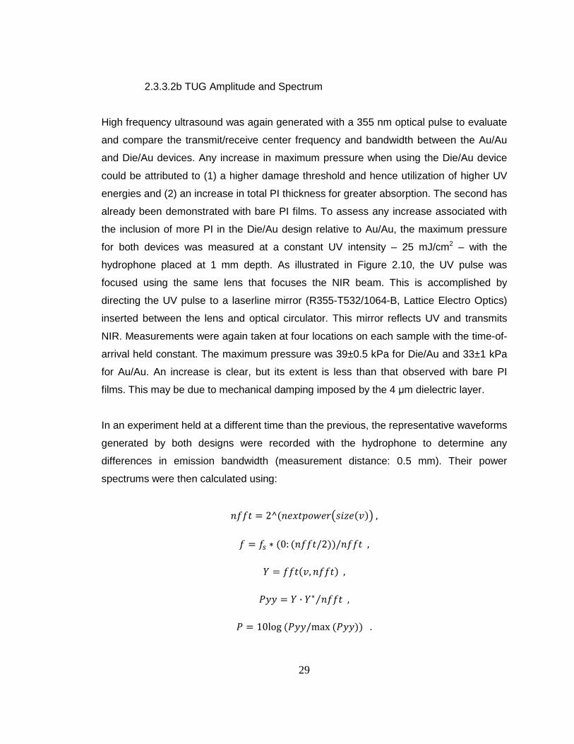
29
2.3.3.2b TUG Amplitude and Spectrum
High frequency ultrasound was again generated with a 355 nm optical pulse to evaluate
and compare the transmit/receive center frequency and bandwidth between the Au/Au
and Die/Au devices. Any increase in maximum pressure when using the Die/Au device
could be attributed to (1) a higher damage threshold and hence utilization of higher UV
energies and (2) an increase in total PI thickness for greater absorption. The second has
already been demonstrated with bare PI films. To assess any increase associated with
the inclusion of more PI in the Die/Au design relative to Au/Au, the maximum pressure
for both devices was measured at a constant UV intensity – 25 mJ/cm2 – with the
hydrophone placed at 1 mm depth. As illustrated in Figure 2.10, the UV pulse was
focused using the same lens that focuses the NIR beam. This is accomplished by
directing the UV pulse to a laserline mirror (R355-T532/1064-B, Lattice Electro Optics)
inserted between the lens and optical circulator. This mirror reflects UV and transmits
NIR. Measurements were again taken at four locations on each sample with the time-of-
arrival held constant. The maximum pressure was 39±0.5 kPa for Die/Au and 33±1 kPa
for Au/Au. An increase is clear, but its extent is less than that observed with bare PI
films. This may be due to mechanical damping imposed by the 4 µm dielectric layer.
In an experiment held at a different time than the previous, the representative waveforms
generated by both designs were recorded with the hydrophone to determine any
differences in emission bandwidth (measurement distance: 0.5 mm). Their power
spectrums were then calculated using:
�\\? � 2^����?O¦§�¨©��ª��d�« , \ � \) ¬ �0: ��\\?/2��/�\\? ,
® � \\?�d, �\\?� , J�� � ® · ®¬ �\\? ,⁄
J � 10log �J��/max �J���� .

where is the voltage waveform,
the complex conjugate of
argument is divisible and adds one.
spectrums are shown in Figure
decreased, so the pressure amplitudes are lower than those previously measured.
However, a larger amplitude observed with the Die/Au design relative to Au/Au is
confirmed. Because of its cutoff frequency at
dominated by the hydrophone’s response. Despite the suppression of the emissions’
bandwidth, the Die/Au spectrum
frequencies greater than 50 MHz.
Figure 2.10. Optical and DAQ setup for detecting TUG resulting from absorption of a UV pulse. In order to integrate ultrasound generation and detection, a mirror that reflects UV and transmits IR is (Dic. Mir.: dichroic mirror).
30
is the voltage waveform, is the sampling frequency, and
of . Nextpower.m finds the largest power of 2 by which its
argument is divisible and adds one. The waveforms and their respective power
in Figure 2.11. Alignment was not optimized and UV energy was
decreased, so the pressure amplitudes are lower than those previously measured.
larger amplitude observed with the Die/Au design relative to Au/Au is
confirmed. Because of its cutoff frequency at 40 MHz, the power
dominated by the hydrophone’s response. Despite the suppression of the emissions’
bandwidth, the Die/Au spectrum appears to exhibit higher power than Au/Au at
frequencies greater than 50 MHz.
Optical and DAQ setup for detecting TUG resulting from absorption of a UV pulse. In order to integrate ultrasound generation and detection, a mirror that reflects UV and transmits IR is inserted between the circulator and focusing lens. (Dic. Mir.: dichroic mirror).
corresponds to
finds the largest power of 2 by which its
respective power
11. Alignment was not optimized and UV energy was
decreased, so the pressure amplitudes are lower than those previously measured.
larger amplitude observed with the Die/Au design relative to Au/Au is
40 MHz, the power spectrums are
dominated by the hydrophone’s response. Despite the suppression of the emissions’
exhibit higher power than Au/Au at
Optical and DAQ setup for detecting TUG resulting from absorption of
a UV pulse. In order to integrate ultrasound generation and detection, a mirror that inserted between the circulator and focusing lens.

2.3.3.2c Directivity
Transmit directivity of both devices was measured
UV spot with a rotational stage. A photograph of the setup is shown in Fig
device with small tank was oriented perpendicular to the table in a larger water tank that
allows angular translation of the hydrop
in the previous measurements was also used in this experiment to maintain the same
spot size. The amplitude of the waveform was recorded throughout a range of
50º relative to normal with a step size of
Figure 2.11. Example waveforms of acoustic emission for (b) Die/Au designs as detected by a 40 MHz hydrophone. The power spectrum for both waveforms is shown in spectrums presented here do not fully because their bandwidth exceeds that of the hydrophone used for detection.
31
Directivity
Transmit directivity of both devices was measured by rotating the hydrophone about the
UV spot with a rotational stage. A photograph of the setup is shown in Fig
device with small tank was oriented perpendicular to the table in a larger water tank that
allows angular translation of the hydrophone about the UV spot. The focusing lens used
in the previous measurements was also used in this experiment to maintain the same
spot size. The amplitude of the waveform was recorded throughout a range of
50º relative to normal with a step size of 1º. 2048 averages were completed at each
Example waveforms of acoustic emission for (a) Au/Au and Die/Au designs as detected by a 40 MHz hydrophone. The power
spectrum for both waveforms is shown in (c). Waveform shape and spectrums presented here do not fully represent the actual signals because their bandwidth exceeds that of the hydrophone used for
by rotating the hydrophone about the
UV spot with a rotational stage. A photograph of the setup is shown in Figure 2.12. The
device with small tank was oriented perpendicular to the table in a larger water tank that
hone about the UV spot. The focusing lens used
in the previous measurements was also used in this experiment to maintain the same
spot size. The amplitude of the waveform was recorded throughout a range of -50º to
1º. 2048 averages were completed at each
Au/Au and
Die/Au designs as detected by a 40 MHz hydrophone. The power Waveform shape and
represent the actual signals because their bandwidth exceeds that of the hydrophone used for

angle using a 1 kHz pulse repetition frequency (
devices are shown in Fig
approximately 30º, though sidelobes are more pro
the curves is caused by imperfect rotational alignment.
The directivity function of an ideal circular transducer is:
where is the wave number,
the first kind. Assuming that the UV spot size did not change when transitioning from the
Au/Au to Die/Au, a change in emission bandwidth is likely responsible for any change in
directivity shape. According to the model, the mainlobe width is reduced and the
sidelobes are enhanced with increasing frequency. The latter is confirmed but the former
is not in the experimental result. This may be due to
single central frequency. The Fraunhoffer zone
2.3 is accurate – begins at a depth of
case, which is significantly smaller than the hydrophone measuring depth.
Figure 2.12. (a) Optomechanical system for detecting transmit directivity(b) zoomed view of rotation mechanism. The UV path is indicated by the violet dashed line, and the axis of rotation is indicated by the white dashed line. Precise alignment of the axis of rotation with the UV spot on the device surface is required. Alignment wtime-of-arrival when rotating the hydrophone.
32
pulse repetition frequency (PRF). The directivity curves for the two
devices are shown in Figure 2.13. Both exhibit a -3 dB transmission angle of
approximately 30º, though sidelobes are more pronounced in the Die/Au. Asymmetry in
the curves is caused by imperfect rotational alignment.
The directivity function of an ideal circular transducer is:
is the wave number, is the radius of the element, and is a Bessel
suming that the UV spot size did not change when transitioning from the
Au/Au to Die/Au, a change in emission bandwidth is likely responsible for any change in
directivity shape. According to the model, the mainlobe width is reduced and the
nhanced with increasing frequency. The latter is confirmed but the former
is not in the experimental result. This may be due to spectrums that do not contain a
single central frequency. The Fraunhoffer zone – the axial distance at which Eq
begins at a depth of . This value is approximately 10 µm in our
case, which is significantly smaller than the hydrophone measuring depth.
Optomechanical system for detecting transmit directivityzoomed view of rotation mechanism. The UV path is indicated by the violet
dashed line, and the axis of rotation is indicated by the white dashed line. Precise alignment of the axis of rotation with the UV spot on the device surface is required. Alignment was verified by observing minimal change in the signal’s
arrival when rotating the hydrophone.
. The directivity curves for the two
3 dB transmission angle of
nounced in the Die/Au. Asymmetry in
is a Bessel function of
suming that the UV spot size did not change when transitioning from the
Au/Au to Die/Au, a change in emission bandwidth is likely responsible for any change in
directivity shape. According to the model, the mainlobe width is reduced and the
nhanced with increasing frequency. The latter is confirmed but the former
that do not contain a
the axial distance at which Equation
. This value is approximately 10 µm in our
case, which is significantly smaller than the hydrophone measuring depth.
Optomechanical system for detecting transmit directivity with
zoomed view of rotation mechanism. The UV path is indicated by the violet dashed line, and the axis of rotation is indicated by the white dashed line. Precise alignment of the axis of rotation with the UV spot on the device surface
as verified by observing minimal change in the signal’s

Receive directivity was not completed at this time due to lack of a rotatable, high
frequency source. A directivity study by Cox and Beard
diameter of an etalon receiver is not always equal to the diameter of NIR illumination,
particularly when the spot radius
this ratio is approximately
estimating the effective spot diameter as shown in Fig
frequency was estimated at 30
being the radius of illumination). Estimating the effective radius from this chart requires a
curve corresponding to a=d/1.6
the red box. The average value on the vertical axis in this region is approximately
, therefore the effective spot diameter is
Die/Au. It is possible that the 43
effective transmit diameter. A more thorough directivity analysis than that presented here
(as in [41]) is required to make this determination.
Figure 2. 13with the (a)
33
Receive directivity was not completed at this time due to lack of a rotatable, high
frequency source. A directivity study by Cox and Beard showed that the effective
diameter of an etalon receiver is not always equal to the diameter of NIR illumination,
particularly when the spot radius is less than twice the etalon thickness [
approximately . Also in [41] is a graphical means of
estimating the effective spot diameter as shown in Figure 2.14a. The central receive
frequency was estimated at 30-40 MHz, therefore the ka value is approximately 2
nation). Estimating the effective radius from this chart requires a
a=d/1.6. The region where is likely to fall is indicated by
the red box. The average value on the vertical axis in this region is approximately
, therefore the effective spot diameter is µm for Au/Au and
It is possible that the 43 µm UV spot also does not accurately represent the
effective transmit diameter. A more thorough directivity analysis than that presented here
]) is required to make this determination.
13. Broadband directivity profiles for a 43 µm UV spot
(a) Die/Au and (b) Au/Au devices [39] (© 2014 IEEE).
Receive directivity was not completed at this time due to lack of a rotatable, high
showed that the effective
diameter of an etalon receiver is not always equal to the diameter of NIR illumination,
less than twice the etalon thickness [41]. In our case,
] is a graphical means of
14a. The central receive
value is approximately 2-3 (a
nation). Estimating the effective radius from this chart requires a
is likely to fall is indicated by
the red box. The average value on the vertical axis in this region is approximately
µm for Au/Au and
m UV spot also does not accurately represent the
effective transmit diameter. A more thorough directivity analysis than that presented here
m UV spot

34
As an estimate for receive directivity, Equation 2.3 is plotted in Fig. 2.14b given the
estimated effective receive diameter and a central frequency of 35 MHz. The -3 dB
transmission angle is approximately 80°. Because th e transmit directivity appears to be
more restricted than the estimated receive directivity, its mainlobe and sidelobes likely
dominate the full transmit/receive directivity profile. An estimate for the complete
transmit/receive response was determined by combining the data in Figure 2.13a and
Figure 2.14b. This curve (Figure. 2.14c) exhibits a -6 dB angle of 45°.
2.3.3.2d Pulse-echo
In order to measure the combined transmit/receive waveform and spectrum, the NIR and
UV beams were enabled simultaneously and then co-aligned in order to transmit and
receive in the same location (Figure 2.15). Alignment is performed using both a course
and fine stage. The former is done using the high-gain 25 MHz probe, and the latter
makes use of the etalon signal generated when the UV pulse heats the etalon layers.
These stages are as follows:
Course:
1. Set up etalon detection with transmitting 25 MHz probe as in Figure 2.9.
2. Change pulser/receiver to receive-only mode without changing probe position.
3. Switch DAQ trigger source from pulser/receiver to UV PD as in Figure 2.10.
4. Steer UV beam using linear actuators connected to mirror mount (Figure 2.15) until
TUG signal detected by 25 MHz probe is maximized.
Fine:
1. Observe etalon detection of thermoelastic signal generated by UV pulse using no
high-pass filtering.
2. Further steer UV beam until low-frequency thermoelastic signal is maximized.
3. Remove 25 MHz probe, and insert reflective target.
4. Directly connect PD output with digitizer (remove amplifier).
5. Increase averaging until SNR is sufficient.
6. Store for post-processing.

Figure 2.14 . (a)element (a: radius of illumination; [41] (© 2007 IEEE). The region inside the red box likely contains the data point for etalons in this study. Shown in profile for a disc element of radius 22 µm at 35 MHz our etalon receiver;
35
. (a) Graphic for estimating the effective radius of an etalon
: radius of illumination; d: etalon thickness; k = wave number) ] (© 2007 IEEE). The region inside the red box likely contains the data
point for etalons in this study. Shown in (b) is the theoretical directivity profile for a disc element of radius 22 µm at 35 MHz – a likely profile for our etalon receiver; (c) full transmit/receive directivity profile for Die/Au.
Graphic for estimating the effective radius of an etalon = wave number)
] (© 2007 IEEE). The region inside the red box likely contains the data the theoretical directivity
a likely profile for ull transmit/receive directivity profile for Die/Au.

Regarding step 1 of the
waveform exemplified by
decaying signal (< 5 MHz) arises from the heating of th
creates thermal expansion of the resonator cavity. Because its time course is on the
order of 100 µs, it is easily separable from the signals of interest by use of filtering.
However, it is useful for the alignment stage becau
easily observable. Concerning
performed between the
amplifier on the PI-etalon’s waveform shape and fr
noting that the reason for using motorized actuators to steer the UV beam is that both
large and very small stepping distances are required, which can be difficult to reproduce
using manual micrometers. They are also e
their adjustment can be automated.
Figure 2.15. Optical and DAQ system for pulse
36
Regarding step 1 of the fine adjustment stage, the thermoelastic signal refers to a
exemplified by that shown in Figure 2.16. The relatively low
decaying signal (< 5 MHz) arises from the heating of the etalon by the UV pulse that
creates thermal expansion of the resonator cavity. Because its time course is on the
order of 100 µs, it is easily separable from the signals of interest by use of filtering.
However, it is useful for the alignment stage because it is of high amplitude and thus
Concerning step 4 of the fine adjustment stage, no amplification is
performed between the PD and the digitizer in order to remove the influence of the
etalon’s waveform shape and frequency content. Finally, it is worth
noting that the reason for using motorized actuators to steer the UV beam is that both
stepping distances are required, which can be difficult to reproduce
micrometers. They are also essential for imaging experiments because
their adjustment can be automated.
Optical and DAQ system for pulse-echo measurements.
ine adjustment stage, the thermoelastic signal refers to a
16. The relatively low-frequency,
e etalon by the UV pulse that
creates thermal expansion of the resonator cavity. Because its time course is on the
order of 100 µs, it is easily separable from the signals of interest by use of filtering.
se it is of high amplitude and thus
ine adjustment stage, no amplification is
and the digitizer in order to remove the influence of the
equency content. Finally, it is worth
noting that the reason for using motorized actuators to steer the UV beam is that both
stepping distances are required, which can be difficult to reproduce
ssential for imaging experiments because

37
A solid metal plate placed at a depth of 1.3 mm served as a reflecting target. The pulse-
echo waveform was recorded with no amplification after 1024 averages, the speed of
which was dictated by the PRF of the Nd:YAG laser (500 Hz). A finite impulse response
(FIR) high pass filter with a cutoff frequency of 2 MHz was then applied to exclude the
thermoelastic response of the etalon. Waveforms were acquired at four randomly-
selected locations on both Au/Au and Die/Au devices and then averaged. Examples are
shown in Figure 2.17a and 2.17b, respectively, with their power spectrums overlaid in
Figure 2.17c. The average center frequency of the Die/Au device was 49±0.6 MHz with
a -6 dB bandwidth of 126±6 %. The center frequency of the Au/Au device was 37±0.8
MHz with a bandwidth of 92±3 %. Added frequency content past 50 MHz with a
secondary peak occurs in the spectrum for Die/Au, which was marginally indicated in the
transmission spectrums in Figure 2.11c. This could signify the presence of two
mechanical resonances associated with the two polymer layers, induced by the high
stiffness of the dielectric mirror.
2.3.3.2e Damage Threshold and Maximum Pressure
The damage threshold of both devices was next determined, and the maximum pressure
generated at breakdown was recorded. Device breakdown was considered to have
occurred after a decrease in the thermoelastic signal of the etalon (Figure 2.16) in
response to increasing UV energy. Following this observation, the UV energy was
measured with a high-sensitivity pyroelectric sensor (J3-09, Molectron), and the
maximum pressure was measured by the hydrophone at a depth of 0.3 mm. Both of
Figure 2.16. Etalon signal corresponding to thermoelastic expansion of its cavity due to absorption of heat generated by the UV pulse.
these measurements were found to vary significantly which prompted the collection of an
additional block of data for both devices, i.e. from a total of eight locations. Assuming a
43 µm UV spot, the average damage thresh
maximum pressure was 213±52 kPa. The damage threshold for Au/Au was 46±8
mJ/cm2 with a maximum pressure of 233±43 kPa. Judging from the standard deviations
of these parameters, the comparison between devices is inconc
precision can be attributed to a non
Figure 2.17.Die/Au designs. Their frequency spectrums are overlaid in 2014 IEEE).
38
these measurements were found to vary significantly which prompted the collection of an
additional block of data for both devices, i.e. from a total of eight locations. Assuming a
m UV spot, the average damage threshold for Die/Au was 45±3 mJ/cm
maximum pressure was 213±52 kPa. The damage threshold for Au/Au was 46±8
with a maximum pressure of 233±43 kPa. Judging from the standard deviations
of these parameters, the comparison between devices is inconclusive. The lack of
precision can be attributed to a non-uniform UV spot, i.e. an illumination profile with
Figure 2.17. Example pulse-echo waveforms for (a) Au/Au and (b)Die/Au designs. Their frequency spectrums are overlaid in (c) (©
these measurements were found to vary significantly which prompted the collection of an
additional block of data for both devices, i.e. from a total of eight locations. Assuming a
old for Die/Au was 45±3 mJ/cm2 and the
maximum pressure was 213±52 kPa. The damage threshold for Au/Au was 46±8
with a maximum pressure of 233±43 kPa. Judging from the standard deviations
lusive. The lack of
uniform UV spot, i.e. an illumination profile with
(b)
(©

39
localized areas of high intensity (Figure 2.2b). When the NIR and UV beams are co-
aligned, these areas may or may not be perfectly coaxial with the NIR spot. If they are
not, breakdown is perceived to have occurred at higher UV energies. If there is in fact a
gain in damage threshold with the Die/Au device, the standard deviations indicate that it
is limited to 12 mJ/cm2.
2.4 Discussion
We have demonstrated here the fabrication and functionality of all-optical HFUS
transducers consisting of a PI thin film deposited underneath an etalon receiver. TUG
was elicited using an 8 ns UV pulse while the etalon operates in the NIR spectrum. The
high absorption at 355 nm and high transmittance at 1550 nm of PI-2555/2525 allows
stable and efficient dual-mode operation. Two designs for the etalon structure were
presented – one with layers Au/SU-8/Au and another with a Dielectric/PI/Au stack. A
dielectric film was chosen to serve as the bottom etalon mirror for its increased NIR
reflectivity and transparency to UV light. This permits the inclusion of a thicker PI layer
without substantially increasing overall device thickness – a choice informed by an
observed 30 % increase in pressure produced by a 10-15 µm film. As summarized in
Table 2.1, the Die/Au design exhibited in an increase in sensitivity (decreased NEP),
frequency content, and output pressure. Improvements in damage threshold and
maximum pressure generated are likely but unconfirmed due to measurement
difficulties.
Improvements in performance notwithstanding, greater steps need to be taken to
establish all-optical transducers as a viable alternative to other ultrasound technologies.
For a comparison in performance, Table 2.1 includes parameters for a collapse-mode
CMUT – another technology suitable for high frequency 2-D arrays due to their ease of
fabrication relative to piezoelectrics [42]. Achievable center frequency and bandwidth is
greater in the optical devices presented and have a similar output pressure. The NEP of
the CMUT was not provided, however CMUTs generally have slightly lower sensitivity
than piezoelectric transducers [43]. The receive characteristics of the Onda hydrophone
(piezoelectric membrane) used in this study are also included in Table 2.1. The NEP of
the hydrophone was estimated (using RMS of noise and V/Pa conversion factor) to be

40
Element Diameter
(µm)
Optical Finesse
NEP
Pa Hz T/R _` (MHz)
T/R -6 dB Bandwidth
(%)
Pressure at } � }P z = 1 mm
(kPa)
Max Pressure @ z(mm)
(kPa)
Damage Threshold (mJ/cm 2)
Au/Au 43 25±2 0.87±0.07 37±0.8 92±3 33±1 233±43 @ 0.3 46±8
Die/Au 43 67±6 0.48±0.05 49±0.6 126±6 39±0.5 213±52 @ 0.3 45±3
CMUT 230* - - 28 90 - 295 @ 0† -
Onda 85 - 1.2 23 (R) 200 (-3dB) - - -
Table 2.1 Comparison of performance parameters between Die/Au and Au/Au PI-etalons. Data represent the average across four locations on the wafer and standard deviation with the exception of Max Pressure and Damage Threshold where eight locations were used. Also shown are parameters for alternative devices with comparable active area and frequency response – a CMUT [42] and the Onda HGL-0085 hydrophone (T/R: Transmit/Receive; E0: 25 mJ/cm2; R: receive-only; z: measurement depth; *Effective diameter calculated from rectangular dimensions; †Half of peak-to-peak measured at device surface) [39] (© 2014 IEEE).
1.2 Pa/Hz1/2 - slightly higher than that for the PI-etalon. The performance of the PI-etalon
is therefore similar to other high frequency technologies with small active area, however
SNR needs more improvement in order to motivate a shift towards laser-based systems.
Many averages are required at present, which is not a practical option for real-time
imaging.
An increase in maximum output pressure could be accomplished by increasing four
parameters associated with the UV beam: spot size, illumination uniformity, wavelength,
and pulse-duration. At the expense of directivity, a larger UV spot in the range of 100-
200 µm will facilitate greater net absorption by lowering intensity. By eliminating localized
areas of high intensity in the beam profile, a uniform illumination will increase
thermoelastic conversion efficiency [44]. Increasing the wavelength and pulse duration
would likely increase the damage threshold, though the latter would reduce transmit
bandwidth. The choice of wavelength is limited by the absorption spectrum of PI-
2525/2555. Using absorbance measurements for the first group of bare PI films, an
absorbance of 1.4 (the value reported for the 2.5 µm PI layer in [37]) was observed for
the 10 µm PI layer at 415 nm – a potential upper limit on useable wavelengths.
Regarding pulse duration, Piglmayer et al. demonstrated that the ablation threshold for a
PI film at 302 nm is nearly constant for pulse widths below 200 ns [45], but this

41
relationship remains to be seen for higher wavelengths. Yung et al. reported an ablation
threshold of 100 mJ/cm2 for a PI film at 355 nm using 21 ns pulses [46]. Assuming that
PI dictates the limit on damage threshold for the overall device, an increase in pulse
width appears justified given our estimate of 45 mJ/cm2 using an 8 ns pulse. However,
damage threshold may be dependent on the particular compound of polyimide used.
Gains in sensitivity will also lend towards a more tenable SNR. Simple alterations that
can decrease the NEP include selecting a PD with lower noise-equivalent power and an
NIR laser with higher output power. Other methods entail further modifying the thin film
structure with alternative fabrication procedures. Relatively simple adjustments for an
improved Q-factor include increasing the etalon thickness and replacing the second
mirror with another dielectric mirror, although disadvantages accompany these
adjustments. Increasing the etalon thickness would decrease bandwidth, and using an
outer dielectric mirror similar in thickness to the first would increase reflections at the
device-medium interface. More drastic changes that could improve sensitivity involve
patterning the films along the lateral dimension. Zhang and Beard showed that the Q-
factor of a fiber optic etalon was considerably increased by creating a convex outer
mirror, producing an NEP of 85 Pa over a bandwidth of 20 MHz (20 mP/Hz1/2) [47].
Tadayon et al. have created a waveguide structure in a polymer etalon that achieved an
NEP of 178 Pa over a bandwidth of 28 MHz (30 mPa/Hz1/2) [48]. These techniques will
be discussed in more detail in Chapter 6.
42
Chapter 3
Imaging with Wafer-based PI-etalons
3.1 Overview
For the first time we demonstrate the viability of an all-optical ultrasound transducer with
supporting optics to form an imaging system yielding the dynamic range required for
tissue imaging. We present the mechanisms, merits, and results of two synthetic-array
configurations created by scanning the receive (NIR) and transmit (UV) beams across
the PI-etalon surface. The first is a fixed-transmitter/scanning-receiver technique wherein
the NIR etalon beam with 35 µm spot is scanned across a 2 x 2 mm aperture upon
which a stationary 2.8 mm UV spot transmits ultrasound in a plane-wave like mode. The
imaging of wire targets placed at a depth of 1.8 mm and 5.2 mm yielded an estimate of
71/145 µm for the lateral resolution and 35/38 µm for the axial resolution in offline
reconstruction. The second system consists of a fixed-receiver/scanning-transmitter
configuration which translates a 43 µm UV spot across of a 2 x 2 mm aperture for each
of four receive locations. Reconstruction of wire targets indicates a lateral resolution of
70/114 µm at depths of 2.4 and 5.8 mm, respectively, with an average axial resolution of
35 µm. Finally, we explore the challenges of imaging in the latter configuration, which
provides the best opportunity for real-time performance pending further development.
3.2 Introduction
We have previously demonstrated the performance of an integrated all-optical
transmitter/receiver consisting of a UV-absorbing PI thin film that is also transparent in
the NIR range – wavelengths used for the operation of etalons in this study. By placing
the PI film underneath an etalon resonator, the UV and NIR beams may overlap yet
independently operate their respective transduction mechanism. As a result, transmitter
and receiver can be in the same location thereby allowing complete 2-D arrays of
arbitrary configuration. To date, linear endoscopic/intravascular ultrasound arrays rarely
exceed operating frequencies above 10 MHz. The adoption of all-optical ultrasound

43
technology therefore has the potential to reveal disease characteristics presently
inaccessible by any endoscopic imaging modality.
The imaging axial resolution provided by an ultrasound transducer array operating with
pulse duration a is
Δª~ d)a2 , where d) is the speed of sound of the medium. Based on the pulse-echo waveforms
presented in Figure 2.17, the average pulse duration between both PI-etalon designs
was approximately 50-60 ns. We can therefore expect an axial resolution in the range of
35-45 µm in water. Lateral resolution is dependent on the aperture of the
transducer/array, imaging depth, and central operating frequency. Typical IVUS
catheters have a diameter below 2 mm in order to be compatible with the size of
peripheral and coronary arteries, so we will limit our lateral region of interest to a 2 x 2
mm rectangular aperture. The -3 dB lateral resolution in the Fraunhofer zone for a flat
rectangular aperture is
�|bµ � 2- sin�. 0.6d)|\] , where R is radial distance, W is the aperture width, and \] is the central operating
frequency [49]. The average central frequency between both PI-etalons was
approximately 43 MHz. At imaging depths of [2 4 6 8 10] mm we can then expect -3 dB
lateral resolutions of approximately [42 84 126 167 209] µm, respectively.
In order to serve as a complete substitute for piezoelectric technology, all-optical arrays
should be capable of receiving at any number of locations simultaneously and likewise
for transmission. This would allow full phased array operation for acoustic beam steering
and focusing in both transmitting and receiving stages. Multiple NIR and multiple UV
beams are then required, which would add significant complexity and cost to the
supporting optical system. A single NIR beam could be split into several beams provided
a constant resonance wavelength at all locations, but a beam splitter and PD would be
required for each channel. A single UV beam could be split in the same way, but optical
multiplexing would be required to turn on and off each subsequent UV beam.

44
In the early 1990’s, techniques using synthetic arrays for ultrasound imaging arose [50].
This typically involves spatially scanning either a single receiver or transmitter while the
other is stationary in order to simulate a full array. Because many fabrication challenges
and performance issues are presented when pursuing dense, high frequency arrays,
synthetic arrays offer a convenient alternative. Using this method, focusing in the
receiving stage can still be performed after all signals have been acquired via delay-and-
sum – a method referred to as the Synthetic Aperture Focusing Technique (SAFT).
However, focusing in transmission is not possible because only a single transmitter can
be active at one time. As a result, both penetration depth and image dynamic range is
lower than that of complete arrays. Another disadvantage is that achieving real time
imaging is more difficult because one must await complete scanning of the aperture
before image reconstruction can begin. Finally, the large separation of A-line
acquisitions in time makes imaging with synthetic arrays more susceptible to motion
artifacts.
Despite the disadvantages intrinsic to synthetic arrays, their convenience in the case of
all-optical ultrasound transduction is substantial. Laser beams can be easily scanned
along the transducer surface using automated translation or steering of optical
components. SAFT imaging is therefore the most practical option at this time. In this
chapter, we explore two types of beam scanning to form synthetic 2-D arrays for 3-D
high resolution imaging. The first involves generating high amplitude acoustic
transmission (> 4 MPa) by using a relatively broad UV spot (approx. 2-3 mm in diameter)
that is fixed in position, and an NIR beam with 35 µm spot is raster scanned within a 2 x
2 mm area superimposed. The second SAFT method involves raster scanning a 43 µm
UV beam across a 2 x 2 mm aperture for each of four different receive locations. The
results presented are such that the Au/Au PI-etalon design was used exclusively for the
fixed-transmitter/scanning-receiver configuration and the Die/Au design for the fixed-
receiver/scanning-transmitter configuration. This is because both the Die/Au design and
its associated scanning technique were hypothesized to be improvements to the imaging
system and thus completed later in time.

45
3.3 Methods and Results
3.3.1 Imaging with Fixed-transmitter/Scanning-receiver
3.3.1.1 Scan Methods and Data Acquisition
In order to scan the NIR beam across a 2-D aperture in an automated fashion, the entire
NIR optical assembly needs to be placed on an x-y-z translation stage that is motorized
in the x-y plane. An illustration of the experimental setup is shown in Figure 3.1a. Linear
actuators (T-LA28A, Zaber Tech.) translate the breadboard on which the NIR optics rest.
The focusing lens has a 60 mm focal length, which provides enough space between the
NIR optics and the etalon to accommodate an unfocused UV beam with angled
incidence. The goal is to raster scan the NIR beam across an aperture that is
superimposed onto the UV spot (Figure 3.1b). As mentioned, the PI-etalon used during
this study had PI/Au/SU8/Au thin film layers with thicknesses of 2.5/0.05/10/0.05 µm,
respectively. For imaging targets, two copper wires having a diameter of 80 µm were
separated and orthogonal to each other in the imaging field. A photograph of the setup is
shown in Figure 3.2.
It should be noted that the UV source used during this imaging study is different than
that on which Chapter 2 results are based. Therefore the pulse-echo duration and
bandwidth are once again worth presenting as they influence imaging resolution. In this
case, the 355 nm optical pulse had a 6 ns pulsewidth, 2.2 mJ energy, and originated
from the third harmonic of a ND:YAG laser (Surelight I, Continuum Inc.). With an incident
angle of roughly 30 degrees, the area of illumination was elliptical with a major diameter
of 3.3 mm and a minor diameter of 2.3 mm yielding an intensity of 36 mJ/cm2. The
amplitude of the generated pressure wave was 4.3 MPa measured at a depth of 1.7 mm.
Using a glass slide as a reflective target, the Au/Au PI-etalon’s pulse-echo (high-pass
filtered at 2 MHz) and spectrum are shown in Figure 3.3. Pulse-echo duration is
approximately 70 ns and the -6 dB spectrum extends from 2 to 48 MHz.

Figure 3.2. Photograph of experimental setup for imaging. Linear actuators (blue arrows) translate a stage on which the NIR optics rest. The unfocused UV beam is stationary and incident upon the PIangle of 30°. Also shownwater tank [37] (© 2012 IEEE).
Figure 3.1. (a) Optical and DAQ system for fixedscan pattern for the NIR spot su
46
Photograph of experimental setup for fixed-transmitter/scanningimaging. Linear actuators (blue arrows) translate a stage on which the NIR optics rest. The unfocused UV beam is stationary and incident upon the PI-etalon with an angle of 30°. Also shown inset is the Au/Au PI-etalon mounted in a small plastic
[37] (© 2012 IEEE).
Optical and DAQ system for fixed-transmitter/scanning-receiver imagingscan pattern for the NIR spot superimposed onto a broad UV spot.
transmitter/scanning-receiver
imaging. Linear actuators (blue arrows) translate a stage on which the NIR optics etalon with an
small plastic
receiver imaging; (b)

Before imaging can be conducted, a map of the resonance wavelengths and their
associated location on the wafer needs to be constructed in order to optimize receive
sensitivity throughout the scan. Resonance wavelength ca
thickness of the etalon is non
water due to uptake of fluid in the etalon cavity. If changes in the resonance wavelength
go unobserved, the operating wavelength of the optic
region of highest slope on the resonance curve. As a consequence, receive sensitivity
can drastically change over the course of the imaging scan and be severely diminished if
the shift is large. Figure
mm scan of the Au/Au transducer at 100 µm intervals. The resonance wavelength was
determined across the intended 2 x 2 mm aperture using 100 µm step size and stored
for the subsequent imaging experiment.
Figure 3.3for Au/Au PI
47
Before imaging can be conducted, a map of the resonance wavelengths and their
associated location on the wafer needs to be constructed in order to optimize receive
sensitivity throughout the scan. Resonance wavelength can vary appreciably if the
thickness of the etalon is non-uniform. It can also shift after immersing the device in
water due to uptake of fluid in the etalon cavity. If changes in the resonance wavelength
go unobserved, the operating wavelength of the optical system may deviate from the
region of highest slope on the resonance curve. As a consequence, receive sensitivity
can drastically change over the course of the imaging scan and be severely diminished if
3.4 portrays the drift of the resonance wavelength across a 1
mm scan of the Au/Au transducer at 100 µm intervals. The resonance wavelength was
determined across the intended 2 x 2 mm aperture using 100 µm step size and stored
for the subsequent imaging experiment.
3.3. Pulse-echo (a) waveform and (b) power spectrum for Au/Au PI-etalon with Continuum Surelight I UV source.
Before imaging can be conducted, a map of the resonance wavelengths and their
associated location on the wafer needs to be constructed in order to optimize receive
n vary appreciably if the
uniform. It can also shift after immersing the device in
water due to uptake of fluid in the etalon cavity. If changes in the resonance wavelength
al system may deviate from the
region of highest slope on the resonance curve. As a consequence, receive sensitivity
can drastically change over the course of the imaging scan and be severely diminished if
of the resonance wavelength across a 1
mm scan of the Au/Au transducer at 100 µm intervals. The resonance wavelength was
determined across the intended 2 x 2 mm aperture using 100 µm step size and stored
power spectrum

48
During the imaging experiment, the NIR probe beam was scanned across the wafer
through a 2 x 2 mm grid using a step size of 30 µm. Before scanning commenced, the
table of resonance wavelengths as a function of beam position was loaded into the
acquisition program. At each grid point in the imaging scan, the LabVIEW DAQ program
searched for the closest corresponding location from which the resonance wavelength
was determined and tuned the wavelength to the associated value minus 1 nm. The PD
output was amplified by 50 dB using the receive function of the pulser/receiver
introduced in Chapter 2. 32 waveforms were acquired at each detector location and
averaged, followed by storage for post-processing. Because the PRF of the Nd:YAG
laser was limited to 10 Hz, total scan time was approximately 4 hours.
3.3.1.2 Post-processing and Image Reconstruction
In addition to the forward-propagating ultrasound created in the PI layer of the device, a
portion propagates backwards through the substrate whereupon it is reflected back
towards the device. Additional acoustic emissions then occur corresponding to each
reflection, and these emissions create additional pulse-echoes off of targets in the
imaging field. These are particularly problematic when large pressures are generated as
when using a broad UV spot for TUG. The first step of post-processing was to null these
additional echoes by searching A-lines for peaks separated in time by the estimated
propagation time through the substrate. The final step of signal processing was to
digitally band-pass filter from 25 to 55 MHz. Delay-and-sum image reconstruction using
SAFT was then performed as follows:
Figure 3.4. Drift of a single resonance over 1 mm at 100 micron step size for the Au/Au device.

49
We define the waveform recorded by a receive element �7, �� as d � d�7, �, ?�, where
continuous time is assumed for convenience. We also define the path taken by the
emitted acoustic wave to pixel �', �, ·� in the imaging field as ¨̧¹¹¹º and represent the return
path of a reflected wave from said pixel to a detector as ̈¹¹¹º (Figure 3.5). In the case of a
broad, unfocused UV spot, assuming plane wave propagation for transmission was
found to provide the best reconstruction results, rather, ¨̧¹¹¹º � ª where ª is referenced to
the detector plane. The shape of the reflected wavefront is assumed to be
isotropic/hemi-spherical, therefore ̈¹¹¹º is a vector from the pixel to the detector. The
presence of a target at �', �, ·� is then indicated by the amplitude N � N�', �, ·�, calculated using
N�', �, ·� � � � d »7, �, ? � ª�·� * | º̈|d) � ?�¼ ,¤½
where
| ̈¹¹¹º| � 2���'� � ��7��� * ����� � ������ * ª�·�� , and ?� is the time of peak UV energy relative to the trigger. This is followed by envelope
detection using ��', �, : � � �7�s�¾�N�', �, : ��� , N¡½��', �, : � � 2��', �, : �� * N�', �, : �� ,
where ¾ is the Hilbert transform. Finally, the data is normalized and subsequently
logarithmized.
The full 3-D reconstruction of the wires can be appreciated via a -10 dB isosurface as
shown in Figure 3.6a. Their relative orthogonality is clear. Figure 3.6b shows 2-D cross
sections of the wires from the 3-D reconstruction with 25 dB dynamic range. We may
observe two types of artifacts, both of which result in the replication of the imaging
targets. The first type is duplication of the nearest wire occurring approximately 1 mm
after the primary reconstruction. This is due to the imperfect removal of reflection
transmissions, as additional signals are buried in noise and hence unidentifiable. A
second artifact is replication of the targets immediately following the original, best
exhibited by the wire at larger depth. These are likely due to the secondary and third
peaks in the pulse-echo waveform shown in Figure 3.3a.

Figure 3.6 . Image reconstruction of dB and (b) orthogonal 2-D slices
Figure 3.5.scanning-receiver image reconstruction. Transmission is assumed to be that of a plane wave, therefore reflected wave front from a hypothetical target at pixel is assumed to be hemispherical and thus travels a distance
to the receiver at (
50
truction of two 80 µm wires in the form of (a) a 3-D isosurface D slices (© 2012 IEEE).
3.5. Acoustic propagation model for fixed-transmitter/
receiver image reconstruction. Transmission is assumed to be that of a plane wave, therefore . The reflected wave front from a hypothetical target at pixel is assumed to be hemispherical and thus travels a distance
to the receiver at (x[m], y[n]).
isosurface at -10
transmitter/ receiver image reconstruction. Transmission is
. The
is assumed to be hemispherical and thus travels a distance

We define imaging resolution by the
estimated by examining 1
full dynamic range is also better appreciated because 8
25 dB. Background noise occurs at approximately 35 dB
previous attempts to image with an all
wire at 1.8 mm, the estimate for the
and 35 µm in the axial dimension. For the wire at 5.2 mm depth, the estimate is 145 µm
in the lateral dimension and 38 µm in the axial dimension.
Figure 3.7. 1-D axial slice of x-z plane in Figure 3.6b showing cross sections of both wires; (b) lateral slice of xlateral slice of y-
51
We define imaging resolution by the -6 dB threshold in the reconstruction, which can be
estimated by examining 1-D cross sections of the 2-D slices as shown in Fig
ge is also better appreciated because 8-bit linear gray scale is limited to
25 dB. Background noise occurs at approximately 35 dB – a far superior result than
previous attempts to image with an all-optical transducer as presented
.8 mm, the estimate for the -6 dB resolution is 71 µm in the lateral dimension
and 35 µm in the axial dimension. For the wire at 5.2 mm depth, the estimate is 145 µm
in the lateral dimension and 38 µm in the axial dimension.
slices of 3-D reconstruction for resolution estimation;z plane in Figure 3.6b showing cross sections of both
lateral slice of x-z plane in Figure 3.6b at nearest wire; (c) -z plane in Fig. 6b at farthest wire.
6 dB threshold in the reconstruction, which can be
D slices as shown in Figure 3.7. The
bit linear gray scale is limited to
a far superior result than
optical transducer as presented in [36]. For the
6 dB resolution is 71 µm in the lateral dimension
and 35 µm in the axial dimension. For the wire at 5.2 mm depth, the estimate is 145 µm
D reconstruction for resolution estimation; (a)
z plane in Figure 3.6b showing cross sections of both

3.3.1.3 Ex Vivo Imaging
To understand how the array might perform in an intravascular setting, an excised
coronary artery of a healthy pig was acquired. The vessel was cut along the direction of
its long axis and flattened
facing the device. Because the aforementioned reflection emissions from the substrate
can substantially affect image reconstruction of continuous media, imaging of the artery
was performed using an Au/Au etalon fabricated on a 10 mm glass substrate. In this
case, the time between the primary emission and the first reflection emission is 4
This allows imaging within a depth of 3
shown in Figure 3.8b, which demonstrates the array’s response to point scatterers of a
turbid media. While penetration depth appears limited to approximately 500 µm, the
result indicates an ability to obtain the SNR required to image organic materials found in
blood vessels. Differentiation of vessel wall components would be expected in disease
models containing layers of fatty and fibrous material from atherosclerotic plaque.
Figure 3.8 Photograph swine, cut along the axial direction and flattened. The red circle in (a) indicates the area imaged.
52
Imaging of Carotid Artery in Swine
To understand how the array might perform in an intravascular setting, an excised
healthy pig was acquired. The vessel was cut along the direction of
its long axis and flattened (Figure 3.8a). The sample was then imaged with the inner wall
facing the device. Because the aforementioned reflection emissions from the substrate
ially affect image reconstruction of continuous media, imaging of the artery
was performed using an Au/Au etalon fabricated on a 10 mm glass substrate. In this
case, the time between the primary emission and the first reflection emission is 4
lows imaging within a depth of 3-4 mm without artifacts. Image reconstruction is
8b, which demonstrates the array’s response to point scatterers of a
While penetration depth appears limited to approximately 500 µm, the
indicates an ability to obtain the SNR required to image organic materials found in
blood vessels. Differentiation of vessel wall components would be expected in disease
models containing layers of fatty and fibrous material from atherosclerotic plaque.
Photograph (a) and reconstruction (b) of an excised coronary artery from swine, cut along the axial direction and flattened. The red circle in (a) indicates the
To understand how the array might perform in an intravascular setting, an excised
healthy pig was acquired. The vessel was cut along the direction of
8a). The sample was then imaged with the inner wall
facing the device. Because the aforementioned reflection emissions from the substrate
ially affect image reconstruction of continuous media, imaging of the artery
was performed using an Au/Au etalon fabricated on a 10 mm glass substrate. In this
case, the time between the primary emission and the first reflection emission is 4-5 µs.
4 mm without artifacts. Image reconstruction is
8b, which demonstrates the array’s response to point scatterers of a
While penetration depth appears limited to approximately 500 µm, the
indicates an ability to obtain the SNR required to image organic materials found in
blood vessels. Differentiation of vessel wall components would be expected in disease
models containing layers of fatty and fibrous material from atherosclerotic plaque.
of an excised coronary artery from
swine, cut along the axial direction and flattened. The red circle in (a) indicates the

53
3.3.2 Imaging with Fixed-receiver/Scanning-transmitter
3.3.2.1 Scan Methods and Data Acquisition
The second beam-scanning technique for SAFT imaging entailed focusing the UV beam
to create a smaller transmit element and spatially scanning it to form a dense synthetic
array. This yields an ability to create both receive and transmit elements at any location.
Figure 3.9 illustrates the optical system for this method, and it is photographed in Figure
3.10. UV and NIR beams are once again integrated as in Chapter 2 for pulse-echo
measurements, however the actuators for automated translation of the NIR assembly
are now in place, and the UV beam will be scanned at regular intervals. As a 355 nm
laser source, we return to the combined 1064/532 nm output of a frequency-doubled
Nd:YAG laser (LUCE, Bright Solutions) guided through a frequency-tripling crystal (LBO
Type 1, Conex Systems Tech.). In addition, the 2.5-50 MHz amplifier of the
pulser/receiver is again used for maximum signal amplitude. Finally, the Die/Au PI-etalon
design was used exclusively under this scanning method, having layers PI/Die/PI/Au/
with 2.5/4/11/0.05 µm thickness.
An important advantage to using this scan method is that the number of receive
elements can be drastically reduced while the UV beam can be scanned through a
dense grid. Recall that scanning the NIR/receive beam throughout a dense grid requires
predetermination of the optimal wavelength at each receive location and imposes added
time to the imaging scan for wavelength adjustments. In using only a few receive
locations, the required wavelength adjustments are minimal, leading to a less complex
imaging procedure and a more stable sensitivity throughout the course of the scan. In
addition, a rapidly scanning galvo-mirror system for the UV laser could be employed that
would lower image acquisition time because there is no need to dwell at the element
location. Lastly, reducing the size of the transmitter creates future opportunities to
explore beam forming with a phased laser array.

Figure 3.10. Photograph of optical system for Again, blue arrows indicate linear actuators
Figure 3.9. Optical and DAQoptics are translated in Cartesian coordinates, while the UV beam is scanned via mirror deflection.
54
Photograph of optical system for fixed-receiver/scanning-transmitter imagingblue arrows indicate linear actuators [39] (© 2014 IEEE).
and DAQ system for fixed-receiver/scanning-transmitter imagingoptics are translated in Cartesian coordinates, while the UV beam is scanned via mirror
transmitter imaging.
imaging. The NIR
optics are translated in Cartesian coordinates, while the UV beam is scanned via mirror

There are a few disadvantages of using a dense grid of small UV spots/transmitters. The
primary one is the lowered acoustic emission associated with a smaller UV spot. We
have compensated for the associated loss in SNR b
high-speed signal acquisition and a laser with higher
transmitter/scanning-receiver setup. Another issue is that translation of the focusing lens
with the NIR optics (used to change the rece
with it. Figure 3.11 shows the intended scan pattern for this study wherein we limit the
number of receive locations to four, and we scan through a dense transmit grid for each
receive location. If we want to use t
location, we have to re-
illustrated in Figure 3.12.
Figure 3.11. Scan pattern intended for fixeddense 2-D grid of transmitting elements This is done by leaving the receive beam at one location and doing the full UV beam scan, followed by translation of the NIR beam to a new location
55
There are a few disadvantages of using a dense grid of small UV spots/transmitters. The
primary one is the lowered acoustic emission associated with a smaller UV spot. We
have compensated for the associated loss in SNR by performing rapid averaging with
speed signal acquisition and a laser with higher PRFs in comparison to the fixed
receiver setup. Another issue is that translation of the focusing lens
(used to change the receive location) also translates the UV beam
11 shows the intended scan pattern for this study wherein we limit the
number of receive locations to four, and we scan through a dense transmit grid for each
receive location. If we want to use the same UV/transmit grid points for each NIR/receive
-center that grid every time the NIR optics are translated, as
can pattern intended for fixed-receiver/scanning-transmitter imaging. of transmitting elements is superimposed on four receive locations
This is done by leaving the receive beam at one location and doing the full UV beam d by translation of the NIR beam to a new location and repeated
There are a few disadvantages of using a dense grid of small UV spots/transmitters. The
primary one is the lowered acoustic emission associated with a smaller UV spot. We
y performing rapid averaging with
in comparison to the fixed-
receiver setup. Another issue is that translation of the focusing lens
slates the UV beam
11 shows the intended scan pattern for this study wherein we limit the
number of receive locations to four, and we scan through a dense transmit grid for each
he same UV/transmit grid points for each NIR/receive
center that grid every time the NIR optics are translated, as
transmitter imaging. A
on four receive locations (a). This is done by leaving the receive beam at one location and doing the full UV beam
and repeated (b).

3-D imaging of two wire targets 127
device using a 2 x 2 mm synthetic aperture of 957 transmitting elements centered on a 1
x 1 mm synthetic array of four receive elements. The two 127 µm wires were oriented
perpendicular to one another and roughly
While the NIR beam is held at a single receive location, the UV beam is scanned across
a 33 x 33 element grid. Prior to the scan, new coordinates representing the center of the
intended transmitter grid (one that i
were predetermined for each receive position. These coordinates were then
Figure 3.12. Beam position adjustments required to maintain the same UV/transmit grid coordinates for all NIR/receive positions. In proper position for the origin of the UV grid, however in translation of the NIR spot, the UV spot is translated as well. The UV beam position must be adjusted
56
D imaging of two wire targets 127 µm in diameter was performed with the Die/Au
device using a 2 x 2 mm synthetic aperture of 957 transmitting elements centered on a 1
x 1 mm synthetic array of four receive elements. The two 127 µm wires were oriented
perpendicular to one another and roughly aligned with an axis of the UV beam scan.
While the NIR beam is held at a single receive location, the UV beam is scanned across
a 33 x 33 element grid. Prior to the scan, new coordinates representing the center of the
intended transmitter grid (one that is centered about the array of four receive elements)
were predetermined for each receive position. These coordinates were then
Beam position adjustments required to maintain the same
UV/transmit grid coordinates for all NIR/receive positions. In (a) we have the proper position for the origin of the UV grid, however in (b) we see that after translation of the NIR spot, the UV spot is translated as well. The UV beam position must be adjusted (c) to regain the original coordinate system.
in diameter was performed with the Die/Au
device using a 2 x 2 mm synthetic aperture of 957 transmitting elements centered on a 1
x 1 mm synthetic array of four receive elements. The two 127 µm wires were oriented
aligned with an axis of the UV beam scan.
While the NIR beam is held at a single receive location, the UV beam is scanned across
a 33 x 33 element grid. Prior to the scan, new coordinates representing the center of the
s centered about the array of four receive elements)
were predetermined for each receive position. These coordinates were then
Beam position adjustments required to maintain the same
we have the we see that after
translation of the NIR spot, the UV spot is translated as well. The UV beam

57
automatically updated when switching to a new receive position during the scan. The
optimal NIR wavelength at each of four receive positions was also predetermined and
programmed into the scan. At each transmit location, 1024 waveforms were amplified by
50 dB, filtered from 2.5-50 MHz, digitized at 250 MHz, and averaged prior to storage for
post-processing. A UV PRF of 500 Hz was used resulting in a total scan time of
approximately two hours.
Accurately knowing the locations of the UV spot during a scan – a prerequisite for high
quality image reconstruction – is challenging because angular deflection of the UV beam
with a mirror mount produces a rhomboidal grid with axes of different step size.
Furthermore, deflection of the beam through a simple plano-convex lens creates a non-
flat focal plane, which introduces scan curvature and a varying spot size. To best
estimate the shape of the 33 x 33 element transmit array, the location of each element in
a downsampled version (99 elements) was estimated using acoustic trilateration. The
hydrophone was used to sample the field generated by each UV element at four
locations laterally dispersed in the target space. The result confirms the presence of two
non-orthogonal scan axes of different step size (Figure 3.13a). Because the axes of
hydrophone translation coincided with those of the NIR scan, the result also
demonstrates the angular offset between the UV array and the NIR array (also shown).
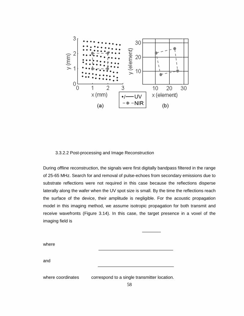
3.3.2.2 Post-processing and Image Reconstruction
During offline reconstruction, the signals were fir
of 25-65 MHz. Search for and removal of pulse
substrate reflections were not re
laterally along the wafer when the UV spot size is small. By the time the reflections reach
the surface of the device, their amplitude is negligible. For the acoustic propagation
model in this imaging me
receive wavefronts (Figure
imaging field is
where
and
where coordinates correspond to a single transmitter location.
Figure 3.13. (a) Receive array (NIR) of transmit array (UV) as determined by acoustic trilateration. The transmit grid used for imaging was of higher density than shown. and transmit arrays (b) are estimated by identifying the UV element that generates the thermoelastic waveform detected by the etalon
58
processing and Image Reconstruction
During offline reconstruction, the signals were first digitally bandpass filtered
65 MHz. Search for and removal of pulse-echoes from secondary emissions due to
substrate reflections were not required in this case because the reflections
laterally along the wafer when the UV spot size is small. By the time the reflections reach
the surface of the device, their amplitude is negligible. For the acoustic propagation
model in this imaging method, we assume isotropic propagation for both transmit and
ure 3.14). In this case, the target presence in a voxel of the
correspond to a single transmitter location.
Receive array (NIR) used for imaging with approximate shape of transmit array (UV) as determined by acoustic trilateration. The transmit grid used for imaging was of higher density than shown. (b) Arrangement of receive
assumed during image reconstruction. Receive locations in (b) are estimated by identifying the UV element that generates the strongest thermoelastic waveform detected by the etalon [39] (© 2014 IEEE).
st digitally bandpass filtered in the range
echoes from secondary emissions due to
quired in this case because the reflections disperse
laterally along the wafer when the UV spot size is small. By the time the reflections reach
the surface of the device, their amplitude is negligible. For the acoustic propagation
thod, we assume isotropic propagation for both transmit and
14). In this case, the target presence in a voxel of the
used for imaging with approximate shape
of transmit array (UV) as determined by acoustic trilateration. The transmit grid rrangement of receive
Receive locations in strongest

Ideally, transmit element locations
results, however the method’s
was assumed to represent the
The relative position of the four receivers (
lines with the strongest thermoelastic signal. The error in using the assumed grid
manifests in a receive grid that is
10 dB isosurface of the 3
3.15a. Figure 3.15b shows two planes of the 3
back side of the wires can be o
the two UV axes, respectively, yielded the best result. From these images, estimates of
6 dB resolution were obtained: 70
114 µm lateral and 38 µ
approximately -30 dB.
Figure receiver/scanning
59
Ideally, transmit element locations and would be determined by trilateration
the method’s accuracy is currently insufficient. A basic linear array that
was assumed to represent the UV grid during reconstruction is shown in Fig
The relative position of the four receivers ( ) can be known by identifying A
lines with the strongest thermoelastic signal. The error in using the assumed grid
manifests in a receive grid that is not square and equally distributed about the center. A
10 dB isosurface of the 3-D reconstruction with 7 µm voxel size is shown in Fig
15b shows two planes of the 3-D reconstruction in which the front and
back side of the wires can be observed. Assuming a UV step size of 72 and 64
the two UV axes, respectively, yielded the best result. From these images, estimates of
6 dB resolution were obtained: 70 µm lateral and 32 µm axial at a depth of 2.4 mm and
m lateral and 38 µm axial at a depth of 5.8 mm. Background noise occurred at
3.14. Propagation model for fixed-
receiver/scanning-transmitter image reconstruction.
would be determined by trilateration
accuracy is currently insufficient. A basic linear array that
s shown in Figure 3.13b.
) can be known by identifying A-
lines with the strongest thermoelastic signal. The error in using the assumed grid
not square and equally distributed about the center. A -
m voxel size is shown in Figure
D reconstruction in which the front and
bserved. Assuming a UV step size of 72 and 64 µm for
the two UV axes, respectively, yielded the best result. From these images, estimates of -
m axial at a depth of 2.4 mm and
al at a depth of 5.8 mm. Background noise occurred at

A smearing artifact typical of backprojection
nearest wire. The source of these effects can be better understood by comparing the
independent reconstructions of data taken a
shows the reconstruction of the nearest wire
receiver positioned at x =
x = 500 µm. Each receiver appears to capture a pulse
µm (lateral) from its position at this
waveform summing of the reconstruction algorithm where the target is not present.
Figure 3.16 also reveals that the orientation of the reconstructed wire differs between
receivers, which may be a consequence
data sets are summed to create Figure
receivers), redundant information between receivers, i.e. echoes received from the same
portion of the wire, fail to sum prop
background levels, including the smearing artifact, and warps the reconstruction of the
target.
Figure 3.15. Image reconstruction of two at -10 dB and (b) orthogonal 2
60
A smearing artifact typical of backprojection algorithms is present, as seen before the
nearest wire. The source of these effects can be better understood by comparing the
independent reconstructions of data taken at single receive positions. Figure
shows the reconstruction of the nearest wire using data collected only by a single
receiver positioned at x = -500 µm. Figure 3.16b shows that for the receiver positioned at
m. Each receiver appears to capture a pulse-echo only within a vicinity of ±500
m (lateral) from its position at this depth, and outside of this vicinity reveals the
waveform summing of the reconstruction algorithm where the target is not present.
16 also reveals that the orientation of the reconstructed wire differs between
receivers, which may be a consequence of using the model in Figure 3.
a sets are summed to create Figure 3.15b (along with data from the remaining two
receivers), redundant information between receivers, i.e. echoes received from the same
portion of the wire, fail to sum properly. This reduces dynamic range that in turn raises
background levels, including the smearing artifact, and warps the reconstruction of the
Image reconstruction of two 127 µm wires in the form of a (a) 3orthogonal 2-D slices [39] (© 2014 IEEE).
algorithms is present, as seen before the
nearest wire. The source of these effects can be better understood by comparing the
t single receive positions. Figure 3.16a
using data collected only by a single
16b shows that for the receiver positioned at
echo only within a vicinity of ±500
depth, and outside of this vicinity reveals the
waveform summing of the reconstruction algorithm where the target is not present.
16 also reveals that the orientation of the reconstructed wire differs between
3.13b. When both
(along with data from the remaining two
receivers), redundant information between receivers, i.e. echoes received from the same
erly. This reduces dynamic range that in turn raises
background levels, including the smearing artifact, and warps the reconstruction of the
3-D isosurface

The complete thermoelastic response of the PI
is best characterized in Figure
a single receiver for one dimension of the UV scan path. Overlap of the UV and NIR
spots is indicated by the earliest and longest
µm). The signal pattern radiating laterally from this point might correspond to flexu
plate waves excited in the dielectric layer. While the presence of these signals aid in
image reconstruction by designating the location of the receivers, they become
problematic when transmitter and receiver are separated by large distances. In this
case, the signals dominate the pulse
thereby overshadowing any echoes reflected from targets within a depth of
approximately 1 mm. Fig
presented in Figure 3.17a. The central frequency of these signals is 20 MHz with a
bandwidth of 120 % –
attenuating the signals of
backwards-travelling acoustic pulse by the rear surface of the 3 mm glass substrate,
represented by the vertical lines near t = 1.1
trigger interference.
Figure 3.16reconstructionConjoining the data creates a reasonable image in Fighowever the comparing (a) and (b) implicates a limiting factor on image quality[39] (© 2014
61
The complete thermoelastic response of the PI-etalon to the absorption of the UV pul
is best characterized in Figure 3.17a. This figure contains pixelated A-lines recorded by
single receiver for one dimension of the UV scan path. Overlap of the UV and NIR
spots is indicated by the earliest and longest-lasting waveform detected
. The signal pattern radiating laterally from this point might correspond to flexu
plate waves excited in the dielectric layer. While the presence of these signals aid in
image reconstruction by designating the location of the receivers, they become
problematic when transmitter and receiver are separated by large distances. In this
ase, the signals dominate the pulse-echo response with substantial delay (
thereby overshadowing any echoes reflected from targets within a depth of
approximately 1 mm. Figure 3.17b shows the average power spectrum of the A
17a. The central frequency of these signals is 20 MHz with a
a frequency range not easily suppressed by filtering without
attenuating the signals of interest. Also depicted in Figure 3.17a is a reflection of the
elling acoustic pulse by the rear surface of the 3 mm glass substrate,
represented by the vertical lines near t = 1.1 µs. Vertical bars near t = 0 correspond to
3.16. Comparison between two receivers of reconstructions whose receive position is indicated by white arrow. Conjoining the data creates a reasonable image in Figure 3.15bhowever the different orientations of the reconstructed wire when comparing (a) and (b) implicates a limiting factor on image quality[39] (© 2014 IEEE).
etalon to the absorption of the UV pulse
lines recorded by
single receiver for one dimension of the UV scan path. Overlap of the UV and NIR
lasting waveform detected (at approx. -500
. The signal pattern radiating laterally from this point might correspond to flexural
plate waves excited in the dielectric layer. While the presence of these signals aid in
image reconstruction by designating the location of the receivers, they become
problematic when transmitter and receiver are separated by large distances. In this
echo response with substantial delay (≈ 1 µs)
thereby overshadowing any echoes reflected from targets within a depth of
17b shows the average power spectrum of the A-lines
17a. The central frequency of these signals is 20 MHz with a -6 dB
a frequency range not easily suppressed by filtering without
17a is a reflection of the
elling acoustic pulse by the rear surface of the 3 mm glass substrate,
s. Vertical bars near t = 0 correspond to
. Comparison between two receivers of 2-D
position is indicated by white arrow. 3.15b,
orientations of the reconstructed wire when comparing (a) and (b) implicates a limiting factor on image quality

3.4 Discussion
We have demonstrated here the basic imaging capabilities of a PI
two beam-scanning methods for a synthetic aperture. Using a 2 x 2 mm synthetic array
of 35 µm receive elements and a broad UV spot, we obtained estimates of 35/38 µm an
71/145 µm at a depth of 1.8/5.2 mm for the axial and lateral resolution, respectively.
Using a dense, 2 x 2 mm synthetic array of transmitters centered on a 1 x 1 mm
synthetic array of four receive elements, results indicate a lateral resolution of 70
Figure 3.17. (a) indicated by pixelated receiver is indicated by the magnitude and duration of the signal generated by the UV pulse. Vertical bars near t = 0 cand those near t = 1.1 of the back of the 3 mm substratepresented in (a) superimposed onto line) [39] (© 2014 IEEE)
62
We have demonstrated here the basic imaging capabilities of a PI-etalon transducer with
scanning methods for a synthetic aperture. Using a 2 x 2 mm synthetic array
of 35 µm receive elements and a broad UV spot, we obtained estimates of 35/38 µm an
71/145 µm at a depth of 1.8/5.2 mm for the axial and lateral resolution, respectively.
Using a dense, 2 x 2 mm synthetic array of transmitters centered on a 1 x 1 mm
synthetic array of four receive elements, results indicate a lateral resolution of 70
Propagation of thermoelastic waveform in etalon layer indicated by pixelated A-lines for a single receiver. Overlap of transmitter with receiver is indicated by the magnitude and duration of the signal generated by the UV pulse. Vertical bars near t = 0 correspond to trigger interference, and those near t = 1.1 µs correspond to reflections of the acoustic pulse off of the back of the 3 mm substrate; (b) average power spectrum of Apresented in (a) superimposed onto Die/Au pulse-echo spectrum (dashed
[39] (© 2014 IEEE).
etalon transducer with
scanning methods for a synthetic aperture. Using a 2 x 2 mm synthetic array
of 35 µm receive elements and a broad UV spot, we obtained estimates of 35/38 µm and
71/145 µm at a depth of 1.8/5.2 mm for the axial and lateral resolution, respectively.
Using a dense, 2 x 2 mm synthetic array of transmitters centered on a 1 x 1 mm
synthetic array of four receive elements, results indicate a lateral resolution of 70 µm and
Propagation of thermoelastic waveform in etalon layer
lines for a single receiver. Overlap of transmitter with receiver is indicated by the magnitude and duration of the signal generated
orrespond to trigger interference, s correspond to reflections of the acoustic pulse off
verage power spectrum of A-lines echo spectrum (dashed

63
114 µm at depths of 2.4 and 5.8 mm, respectively, with an average axial resolution of 35
µm. Results from both imaging configurations correlate well to the expected resolutions
presented in the introduction, and they mark an advance in the ability of an all-optical
device to provide the dynamic range needed for high resolution ultrasound imaging.
Both imaging configurations presented here have advantages and disadvantages. With
a broad UV spot and dense receive (NIR) array, acoustic output is easily greater than 1
MPa, which maximizes SNR. In addition, the propagation model for image reconstruction
is more accurate with the fixed-transmitter/scanning-receiver because the exact
locations of each receive element are predictable, which improves image quality.
However, receive sensitivity is unstable due to a severe variation in resonance
wavelength across the wafer. It is therefore likely that the user would have to calibrate
often by finding the resonance wavelength for each of many receive locations so as to
avoid significant drops in sensitivity. Finally, frequent translation of the entire NIR optical
assembly may introduce alignment errors. Specifically, the device plane may drift out of
the NIR focal plane, and coupling of the reflected NIR beam to the PD may shift away
from optimal alignment.
Scanning the UV beam for a dense array of transmitters is advantageous in that there is
no need for frequent wavelength adjustments. Furthermore, maintaining alignment is
less critical because the NIR assembly is only translated to a small number of positions
for receiving. Consequently, a high-speed galvo scanner can be integrated into the setup
to do the bulk of the beam scanning. Using a galvo for the NIR beam is much more
challenging because of the need to capture the reflection. The primary disadvantage in
using a fixed-receiver/scanning-transmitter configuration is the lowered acoustic output
associated with a small UV spot size. This diminishes SNR thereby requiring a high level
of averaging. In addition, precise determination of the transmitter locations across the
scan aperture for an accurate propagation model is difficult in the scanning-transmitter
arrangement. The grid of elements in the 2-D scan is not rectilinear, and the pitch varies
throughout. These factors ultimately degrade image quality during reconstruction
because of (1) errors in estimating the propagation time to and from a pixel in the field of
view and (2) ineffective summing of datasets between individual receivers whose UV
coordinate systems are not the same.

64
At this time, we believe that the potential speed of the scanning-transmitter/fixed-
receiver arrangement warrants our focus, as real-time imaging is the final goal. Also its
disadvantages may be mitigated by various techniques. As mentioned in Chapter 2,
SNR can be enhanced by increasing UV illumination uniformity, spot size, and pulse
duration. Lateral confinement of the etalon resonator will also increase SNR. Though
modifications of this nature will create additional alignment challenges, maintaining only
a few receivers that are fixed in location would limit them.
A more predictable UV scan grid could be achieved by modifying the system optics.
Figure 3.18 illustrates the detriments of scanning with a conventional lens compared to
different types of scanning lenses. Using a simple achromatic lens results in a non-flat
focal plane (Figure 3.18a). Spot size and the scanning step size are therefore
inconsistent. Flat-field scanning lenses (Figure 3.18b) resolve this issue, but scan length
isn’t linear with input angle (step � \ tan À). F-theta lenses (Figure 3.18c) add elements
such that the relationship between incident angle and step size is linear, while telecentric
f-theta lenses (Figure 3.18d) accomplish the same feat while maintaining a beam that is
always orthogonal with the focal plane. In our case, the desired scan field is less than 5
x 5 mm. If we choose to maintain a lens focal length in the range of 30-60 mm, the
maximum scan angle is less than 10°. At this angle, \À Á \ tan À and the telecentric lens
would be of less benefit. Moreover, a single-element scan lens is desirable because it
would (1) allow for less distance between the NIR PBS and focusing lens (optimal for
maintaining NIR alignment) and (2) reflect less energy at wavelengths for which it is not
designed (less components = less reflections). Regarding the latter feature, scanning
lenses supporting such a broad wavelength range (355-1550 nm) do not exist. Because
we currently have less NIR energy to spare, the best choice might be a flat-field
scanning lens for 1550 nm and to accept energy losses at 355 nm. However, it is
unknown to what degree a flat focal plane will be maintained at 355 nm. If an NIR source
with higher power is obtained, a lens designed for 355 nm will likely be best.

Transitioning to non-metallic targets
SNR, therefore the aforementioned modifications might
insufficient, we might revert to the fixed
broad UV spot for higher acoustic output. We anticipate that creating a fiber optic
equivalent of our device for
on SNR. Coupling the laser beams to a f
as well as the shape and density of the arrays
An obstacle that may generally
the scan time associated with synthetic apertures. When using the
in the fixed-receiver/scanning
sampling 10 µs of data at 250 MHz is approximately 2.5 kHz. Assuming that large gains
in SNR can be achieved and the scan is limited purely by data acquisi
performing 32 averages (versus 1024) with a 2.5 kHz PRF (versus 500 Hz) would
reduce scan time from two hours to 50 seconds. Without gains in SNR, a field
programmable gate array could be employed to perform a high level of averaging thus
reducing data transmission over the PXI bus. This would allow for a PRF beyond 2.5
kHz. It is also possible to lower the density of the UV grid and incorporate multiple NIR
lasers to reduce scan time. Decreasing the density by a factor of two (255 elements
versus 957) and using four NIR laser systems would further lower scan time to 4
Figure 3.18. Different scan lens types spaced grids [51].
65
metallic targets such as tissue will introduce high
the aforementioned modifications might be necessary. If SNR is still
insufficient, we might revert to the fixed-transmitter/scanning-receiver configuration with
broad UV spot for higher acoustic output. We anticipate that creating a fiber optic
equivalent of our device for in vivo use will be challenging and place further constraints
oupling the laser beams to a fiber bundle will limit the optical energy available
as well as the shape and density of the arrays.
generally prevent the adoption of all-optical ultrasound imaging is
the scan time associated with synthetic apertures. When using the PXI acquisition card
receiver/scanning-transmitter study, the maximum trigger rate when
s of data at 250 MHz is approximately 2.5 kHz. Assuming that large gains
in SNR can be achieved and the scan is limited purely by data acquisi
performing 32 averages (versus 1024) with a 2.5 kHz PRF (versus 500 Hz) would
reduce scan time from two hours to 50 seconds. Without gains in SNR, a field
programmable gate array could be employed to perform a high level of averaging thus
reducing data transmission over the PXI bus. This would allow for a PRF beyond 2.5
kHz. It is also possible to lower the density of the UV grid and incorporate multiple NIR
lasers to reduce scan time. Decreasing the density by a factor of two (255 elements
versus 957) and using four NIR laser systems would further lower scan time to 4
ifferent scan lens types to consider for achieving orthogonal, regularly
will introduce higher demands on
be necessary. If SNR is still
receiver configuration with
broad UV spot for higher acoustic output. We anticipate that creating a fiber optic-
place further constraints
iber bundle will limit the optical energy available
optical ultrasound imaging is
PXI acquisition card
transmitter study, the maximum trigger rate when
s of data at 250 MHz is approximately 2.5 kHz. Assuming that large gains
in SNR can be achieved and the scan is limited purely by data acquisition parameters,
performing 32 averages (versus 1024) with a 2.5 kHz PRF (versus 500 Hz) would
reduce scan time from two hours to 50 seconds. Without gains in SNR, a field-
programmable gate array could be employed to perform a high level of averaging thus
reducing data transmission over the PXI bus. This would allow for a PRF beyond 2.5
kHz. It is also possible to lower the density of the UV grid and incorporate multiple NIR
lasers to reduce scan time. Decreasing the density by a factor of two (255 elements
versus 957) and using four NIR laser systems would further lower scan time to 4
to consider for achieving orthogonal, regularly-

66
seconds. At this time scale, the mechanical scan rate of the actuators can also be a
limiting factor. Modern galvo scanners can scan at a rate below 1 ms per step. In this
case, scanning through a 957-element array once would take 1 second. Time for image
reconstruction should also be addressed. Producing a single 2-D slice with our 64-bit,
3.4 GHz quad-core PC took 33 seconds. Halving the UV-grid density reduces
reconstruction time to 10 seconds, however background levels in the image increase
from -30 to -25 dB. Utilizing GPU processing and an increased pixel size would lower it
to below 1 second. Additional ways to increase frame rate might be to introduce sparse
arrays or add frequency-domain SAFT reconstruction [52].

67
Chapter 4
Fiber Optic Etalon for Photoacoustic Imaging
4.1 Overview
In this work we present the fabrication and testing of a fiber optic ultrasound sensor
based on etalon technology. In between two Au mirrors, SU-8 polymer was spray coated
onto the face of a single mode (SM) fiber to form the etalon medium with 13 µm
thickness and a finesse of 22. Using a broadband signal to evaluate its performance, the
sensitivity was 11.6 kPa over a 47.5 MHz bandwidth, or 1.7 Pa/Hz1/2 with a -3 dB
bandwidth of 27 MHz centered at 28 MHz. We propose the development of a rectilinear
ultrasound array based on this device. The design entails the bundling of several fiber
etalons which, when combined with photoacoustic excitation, would yield a flexible and
compact, forward-viewing photoacoustic endoscope. To simulate the performance of a
bundled device, we have mechanically scanned a single fiber etalon to image simple
photoacoustic targets. The results demonstrate the viability of using a fiber optic-based
photoacoustic endoscope to image optically absorptive structures such as blood in
vasculature. Potential applications for our device include the monitoring of angiogenesis
and hypoxia, which are early markers of tumor formation.
4.2 Introduction
Photoacoustic imaging (PAI) is a versatile modality that has been used in a variety of
medical applications involving both anatomical and functional visualization of biological
processes. The positive attributes of this modality include the high-specificity of optical
imaging and the high resolution and low scattering of ultrasound imaging. By choosing a
particular irradiation wavelength, specific structures can be selected for imaging with
high contrast due to their characteristic absorption at that wavelength. Blood for example
is highly absorptive of green light, and the imaging of microvasculature has been
demonstrated by several research groups using PAI [53-55]. These structures, owing to
their micro-scale dimensions, emit high-frequency ultrasound waves (> 20MHz). In

68
addition to a choice of morphology, PAI can be tailored to image the distribution of
oxygen in tissue thereby revealing spatial information on metabolic processes [56].
4.2.1 Angiogenesis
Angiogenesis is vital for the formation, growth, and survival of tumor masses in cancer
[57]. Several pharmacological mechanisms have been employed in attempting to
prevent or reduce the formation of vasculature required for tumor growth as part of a
therapeutic regimen. The predominant method has been to target the signaling
pathways of vascular endothelial growth factor (VEGF) [58], and several drugs such as
Bevacizumab have been approved by the Food and Drug Administration (FDA) as safe
and effective treatments for anti-angiogenic therapy [59]. However, monitoring the
microscopic effects of these treatments in vivo has proven to be challenging with
conventional vascular imaging techniques such as dynamic contrast-enhanced (DCE-)
MRI or X-ray CT [60]. Evaluating angiogenic criteria including microvascular density and
vascular heterogeneity escape the resolution of these techniques and often require
histological examination. PAI is a valuable compromise between the invasive surgery
required for histological analysis and the limited resolution of DCE-MRI/CT. An
endoscopic method could potentially facilitate repeated access to cancerous areas for
the three-dimensional imaging of microvasculature. PAI could therefore prove useful in
characterizing angiogenic activity and thus the effectiveness of angiogenesis inhibitors in
curtailing tumor growth.
4.2.2 Hypoxia
Cancerous tissue has been shown to be significantly more hypoxic than normal tissue
due to poor vascularization. While hypoxia in normal tissue typically results in
programmed cell death, cancer cells often respond by overexpressing hypoxia-inducible
factor 1 proteins (HIF-1) which has been correlated with increased tumor growth,
metastasis, and recurrence [61], [62]. Hypoxia furthermore increases resistivity to
radiation therapy due to the role oxygen plays in enabling the free-radical damage of
DNA [63]. Because chemotherapy specifically targets rapidly proliferating cells, the
slowed rate of cell growth resulting from hypoxia also limits response to treatment.

69
Hypoxia therefore has arisen to be a factor in cancer prognosis as well as a predictor of
treatment viability, and it can be estimated by measuring pO2. Techniques such as fMRI,
F19-labeled MRI, and positron emission tomography (PET) have been used to image
hypoxia, however they only provide qualitative measurements of pO2 and are moreover
a costly option for repeated studies [64]. The detection of pO2 via Photoacoustic Lifetime
Imaging (PALI) is a method pioneered by our group [65], [66]. This method entails a
double-pulse excitation of oxygen-sensitive dyes to produce an acoustic signal from
which absolute pO2 can be inferred. With the addition of a dye-administering channel,
PALI could be integrated into our design for a photoacoustic endoscope. It could
therefore be used in vivo for high-resolution imaging of pO2 in combination with vascular
imaging. The ability to endoscopically image both the degree of hypoxia and states of
angiogenesis in cancer patients with a single device could prove to be a powerful
diagnostic tool in the staging, treatment, and monitoring of malignant growths.
4.2.3 Photoacoustic Endoscopy
Photoacoustic Endoscopy (PAE) is a new imaging modality that can provide high-
resolution vascular imaging in vivo. Yang et al. have created the first photoacoustic
endoscope, consisting of a radially scanning probe combined with linear translation in
order to perform 3-D vascular imaging [67], [68]. However, the rigidity of the device’s 48
mm-long probe head may significantly limit the number of viable endoscopic applications
due to a requisite flexibility for fine guidance. Radial devices are also restricted in that
they cannot image areas directly in front of the probe as with traditional endoscopes. In
this work, we demonstrate an alternative design for PAE based on fiber optics for the
purposes of creating a flexible, forward-viewing imager. This device design could be
used to navigate through both lumen and body cavities with minimal invasiveness. We
will moreover use 532 nm optical pulsing for photoacoustic excitation and thus perform
vascular imaging, as blood is highly absorptive at this wavelength.
For the development of a forward-viewing photoacoustic endoscope, we propose the
inclusion of etalon transducers for high-frequency detection. Unlike other existing
technologies, these sensors maintain high sensitivity at high frequencies despite a
reduced transducer size. Furthermore, the simplicity of etalon receivers makes them

70
highly miniaturizable, and a few groups have successfully fabricated etalons onto the tip
of optical fibers to be used for low-field acoustic detection [69]-[72]. Our design entails
the fabrication and bundling of several fiber etalons to form a high-frequency ultrasound
sensor array for high-resolution imaging. The conjoining of a fiber etalon bundle with one
or several fibers that transmit optical pulses would serve as a flexible and compact
photoacoustic endoscope. Previous etalons created by our group have been shown to
have bandwidths above 50 MHz [16], which corresponds to an axial imaging resolution
of 30 µm. At this scale, our endoscopic device would prove useful in vascular and
functional imaging in vivo.
4.3 Methods and Results
4.3.1 Fabrication
Nanofabrication techniques are commonly used to construct optical resonators of small
thickness, and these techniques were used to deposit the etalon’s layers onto the tip of
an optical fiber. A standard SM fiber was stripped to its 120 µm cladding and cleaved to
provide a flat surface on which to fabricate the etalon. Electron-beam evaporation was
then used for deposition of the first etalon mirror. A 3 nm titanium adhesion layer was
first evaporated onto the tip of the optical fiber followed by a 30 nm layer of gold for high
reflectivity. SU-8 photoresist was chosen for the optical medium due to the polymer’s
high compressibility and thus sensitivity to acoustic pressure. Microchem’s MicroSpray
was used to manually spray coat SU-8 after deposition of the first mirror. An
approximate thickness of 10 µm has shown to provide an optimal tradeoff between
bandwidth and sensitivity in previous etalons [18], and a single spray of MicroSpray was
found to have deposited a 10-15 µm layer of SU-8 at the fiber tip. Due to the surface
tension of the cylindrical fiber, the shape of the layer formed is convex. After deposition,
the layer is cured and exposed to UV light to initiate cross linkage. Finally, a second
mirror was evaporated in order to complete the construction of the resonator (Figure 4.1
inset).

4.3.2 Characterization
4.3.2.1 Optical Resonance
To measure the optical resonance of the etalon, a wavelength
(Agilent HP 8168F) was connected to a fiber optic circulator
FC) at port 1 (Figure 4.1)
connector, and the reflected signal is routed through Port 3 and detected b
PD (New Focus 1811-FC) that has both AC (> 25 kHz) and DC (< 25 kHz) outputs. The
DC output was monitored by a multimeter. The resonance profile can be observed in
Figure 4.2. The optical finesse was approximately
100 nm as seen in the resonance curve, the thickness of the cavity can be estimated
using
where and are the wavelengths at resonance and
reflected power is lowered due to the reduced coupling and attenuation by the fiber optic
circulator; an input power of 2 mW at 1550 nm yielded 1.05 mW returned for the fiber,
whereas 1.25 mW was detected using the free space/wafer setup.
Figure 4.1 . Optical and DAQ system for resonance measurement of fiber optic etalon with photograph of device, inset. The spraysurface. However, optical propagation is limited to the cavity section just above the 9 µm core. (FOC: fiber optic circulator; PD: photodetector with DC and AC outputs; p1/p2/p3: ports 1/2/3).
71
4.3.2 Characterization
4.3.2.1 Optical Resonance
o measure the optical resonance of the etalon, a wavelength-tunable
(Agilent HP 8168F) was connected to a fiber optic circulator (FOC) (Thor Labs 6015
(Figure 4.1). Port 2 was connected to the fiber optic etalon with an FC
connector, and the reflected signal is routed through Port 3 and detected b
FC) that has both AC (> 25 kHz) and DC (< 25 kHz) outputs. The
DC output was monitored by a multimeter. The resonance profile can be observed in
2. The optical finesse was approximately 22. Given the FSR of approxima
100 nm as seen in the resonance curve, the thickness of the cavity can be estimated
are the wavelengths at resonance and is the index of refraction. The
ed power is lowered due to the reduced coupling and attenuation by the fiber optic
circulator; an input power of 2 mW at 1550 nm yielded 1.05 mW returned for the fiber,
whereas 1.25 mW was detected using the free space/wafer setup.
. Optical and DAQ system for resonance measurement of fiber optic etalon with photograph of device, inset. The spray-coated polymer layer forms a concave surface. However, optical propagation is limited to the cavity section just above the 9
fiber optic circulator; PD: photodetector with DC and AC outputs;
tunable CW NIR laser
(Thor Labs 6015-3-
. Port 2 was connected to the fiber optic etalon with an FC-FC
connector, and the reflected signal is routed through Port 3 and detected by a 125 MHz
FC) that has both AC (> 25 kHz) and DC (< 25 kHz) outputs. The
DC output was monitored by a multimeter. The resonance profile can be observed in
. Given the FSR of approximately
100 nm as seen in the resonance curve, the thickness of the cavity can be estimated
is the index of refraction. The
ed power is lowered due to the reduced coupling and attenuation by the fiber optic
circulator; an input power of 2 mW at 1550 nm yielded 1.05 mW returned for the fiber,
. Optical and DAQ system for resonance measurement of fiber optic etalon
coated polymer layer forms a concave surface. However, optical propagation is limited to the cavity section just above the 9
fiber optic circulator; PD: photodetector with DC and AC outputs;

72
4.3.2.2 Acoustic Performance
In order to evaluate its acoustic performance, the fiber etalon was submerged in a water
tank and placed near a 100 nm chromium thin-film irradiated with a 3 ns, 532 nm laser
pulse generated by a Nd:YAG laser (Bright Solutions LUCE). The setup is shown in
Figure 4.3. A photoacoustic source was chosen because it produces a broad band
signal suitable for evaluating the frequency response of the etalon. In addition, alignment
of the etalon with such a source is significantly easier with a fiber device compared to
the wafer design. To achieve maximum sensitivity, the wavelength of the IR beam was
adjusted to that corresponding to the point of minimum slope on the falling edge of the
resonance curve. The AC output of the PD was then sampled at 250 MHz with an 8-bit
digitizer (PXI-5114, National Instruments Corp.) and averaged 1024 times with no
amplification.
Figure 4.2. Normalized resonance profile of fiber optic etalon (a.u.: arbitrary units).

Figure 4.4b shows the temporal waveform detected by the fiber etalon. Because the
metallic film is very thin, the acoustic field generated conforms to the energy profile of
the optical pulse, as seen in Fig
4.4b corresponds to what is expected in this case, but several oscillations occur
thereafter. These are likely due to additional resonant modes (mechanical) occurring in
the convex polymer slab, which are represented by the periodic dips in the waveform’s
power spectrum (Figure
but truncated after the first oscillation
a flat thin film. The center frequency of this spectrum is 27.5 MHz with a
of 27 MHz or 98 %. The NEP was determined by measuring the maximum pressure
generated by the irradiated film using
NEP was 11.6 kPa over a 47.5 MHz bandwidth or 1.7 Pa/Hz
1.3 Pa/Hz1/2 obtained using the wafer etalon (~9 kPa). This is likely due to the reduction
in reflected power caused by increased attenuation in the
Figure 4.3. Optical and DAQ setup for evaluating sensitivity and spectrum of fiber etalon. A chromium thin film irradiated with a 532 nm optical pulse was used as a broad band acoustic source, and the film was illuminated on the side opposite to the fiber etalon.
73
the temporal waveform detected by the fiber etalon. Because the
metallic film is very thin, the acoustic field generated conforms to the energy profile of
the optical pulse, as seen in Figure 4.4a. The first bipolar oscillation present in Fig
esponds to what is expected in this case, but several oscillations occur
thereafter. These are likely due to additional resonant modes (mechanical) occurring in
the convex polymer slab, which are represented by the periodic dips in the waveform’s
4.4c). Overlaid on this spectrum is that for the same waveform
but truncated after the first oscillation – a more ideal response that can be expected from
a flat thin film. The center frequency of this spectrum is 27.5 MHz with a
of 27 MHz or 98 %. The NEP was determined by measuring the maximum pressure
generated by the irradiated film using the calibrated hydrophone (Onda HGL
NEP was 11.6 kPa over a 47.5 MHz bandwidth or 1.7 Pa/Hz1/2 – slightly higher than the
obtained using the wafer etalon (~9 kPa). This is likely due to the reduction
in reflected power caused by increased attenuation in the FOC.
Optical and DAQ setup for evaluating sensitivity and spectrum of fiber etalon. A chromium thin film irradiated with a 532 nm optical pulse was used as a broad band acoustic source, and the film was illuminated on the side opposite to the fiber
the temporal waveform detected by the fiber etalon. Because the
metallic film is very thin, the acoustic field generated conforms to the energy profile of
a. The first bipolar oscillation present in Figure
esponds to what is expected in this case, but several oscillations occur
thereafter. These are likely due to additional resonant modes (mechanical) occurring in
the convex polymer slab, which are represented by the periodic dips in the waveform’s
on this spectrum is that for the same waveform
a more ideal response that can be expected from
a flat thin film. The center frequency of this spectrum is 27.5 MHz with a -3 dB bandwidth
of 27 MHz or 98 %. The NEP was determined by measuring the maximum pressure
calibrated hydrophone (Onda HGL-0085). The
slightly higher than the
obtained using the wafer etalon (~9 kPa). This is likely due to the reduction
Optical and DAQ setup for evaluating sensitivity and spectrum of fiber
etalon. A chromium thin film irradiated with a 532 nm optical pulse was used as a broad band acoustic source, and the film was illuminated on the side opposite to the fiber

To verify that the extra oscillations in the chromium waveform were due to additional
mechanical modes in the curved etalon cavity and not a part of the actual acoustic field,
a 25 MHz transducer (active area: 12.5 mm;
Inc.) driven by a pulser/receiver (bandwidth: 50 MHz; DPR300, JSR Ultrasonics) was
Figure 4.4. (a) TUG waveform detected by fiber etalon. The waveform’s spectrum is shown in (c). Overlaid on the spectrum is that for the waveform in (b) truncated after the first bipolar oscillation.
74
To verify that the extra oscillations in the chromium waveform were due to additional
mechanical modes in the curved etalon cavity and not a part of the actual acoustic field,
a 25 MHz transducer (active area: 12.5 mm; focal length: 25.4 mm; V324, Olympus NDT
Inc.) driven by a pulser/receiver (bandwidth: 50 MHz; DPR300, JSR Ultrasonics) was
4.4. (a) Energy profile of the optical pulse that generated the TUG waveform detected by fiber etalon. The waveform’s spectrum is
Overlaid on the spectrum is that for the waveform in (b) truncated after the first bipolar oscillation.
To verify that the extra oscillations in the chromium waveform were due to additional
mechanical modes in the curved etalon cavity and not a part of the actual acoustic field,
focal length: 25.4 mm; V324, Olympus NDT
Inc.) driven by a pulser/receiver (bandwidth: 50 MHz; DPR300, JSR Ultrasonics) was
Energy profile of the optical pulse that generated the (b)
TUG waveform detected by fiber etalon. The waveform’s spectrum is Overlaid on the spectrum is that for the waveform in (b)

used as an acoustic source. The reflection of the transmitted acoustic signal off of the
etalon face is shown in Fig
Figure 4.5b. The etalon signal was amplified by
settings for the echo. Oscillat
indicating modulation of the true ac
4.3.3 PAI with a Synthetic Aperture
In an effort to estimate the performance of a fiber etalon bundle in the imaging of
photoacoustic targets, the fiber etalon was translated in a 2
target plane by connecting linear actuators to the Cartesian translation stage on which
the device is mounted (Figure
was fixed during the scan, and the pulser/receiver was used to amplify the AC output
the PD. The first target imaged was a black polystyrene sphere of diameter 50 µm
embedded in agarose gel. The sphere was illuminated using a 532 nm optical pulse at a
Figurereflected off of fiber etalondetected by the fiber etalon.
75
used as an acoustic source. The reflection of the transmitted acoustic signal off of the
etalon face is shown in Figure 4.5a, and that detected by the etalon can be observed in
5b. The etalon signal was amplified by the pulser/receiver using the same
settings for the echo. Oscillations additional to those in Figure 4.5a are clearly present,
indicating modulation of the true acoustic waveform received.
Synthetic Aperture
In an effort to estimate the performance of a fiber etalon bundle in the imaging of
photoacoustic targets, the fiber etalon was translated in a 2-D plane parallel with the
t plane by connecting linear actuators to the Cartesian translation stage on which
(Figure 4.6). Illumination of targets for photoacoustic excitation
was fixed during the scan, and the pulser/receiver was used to amplify the AC output
. The first target imaged was a black polystyrene sphere of diameter 50 µm
embedded in agarose gel. The sphere was illuminated using a 532 nm optical pulse at a
ure 4.5. (a) Pulse-echo of 25 MHz probe
reflected off of fiber etalon and (b) the waveform detected by the fiber etalon.
used as an acoustic source. The reflection of the transmitted acoustic signal off of the
at detected by the etalon can be observed in
pulser/receiver using the same
5a are clearly present,
In an effort to estimate the performance of a fiber etalon bundle in the imaging of
D plane parallel with the
t plane by connecting linear actuators to the Cartesian translation stage on which
6). Illumination of targets for photoacoustic excitation
was fixed during the scan, and the pulser/receiver was used to amplify the AC output of
. The first target imaged was a black polystyrene sphere of diameter 50 µm
embedded in agarose gel. The sphere was illuminated using a 532 nm optical pulse at a

1 kHz PRF to allow for fast averaging. During the scan, a 1 mm x 1 mm plane was
traversed above the bead at 30 µm intervals. This corresponded to a hypothetical array
of 1225 elements. Image reconstruction was then performed using
. Signals were first filtered using a 2.5
diameter of the reconstructed bead according to the three dimensions x (lateral), y
(lateral), and z (axial) was approximately 75, 125, and 200 µm, respectively (Fig
Illumination was incident
Figure 4.7. Orthogonal 2-532 nm pulse.
Figure 4.6. Optical and DAQ target using fiber etalon.
76
1 kHz PRF to allow for fast averaging. During the scan, a 1 mm x 1 mm plane was
rsed above the bead at 30 µm intervals. This corresponded to a hypothetical array
of 1225 elements. Image reconstruction was then performed using Equation 3.1
. Signals were first filtered using a 2.5-50MHz asymmetric FIR filter. The
diameter of the reconstructed bead according to the three dimensions x (lateral), y
(lateral), and z (axial) was approximately 75, 125, and 200 µm, respectively (Fig
from the positive y direction.
-D reconstructions of 50 µm polystyrene bead illuminated with a
l and DAQ system for synthetic aperture imaging of a photoacoustic
1 kHz PRF to allow for fast averaging. During the scan, a 1 mm x 1 mm plane was
rsed above the bead at 30 µm intervals. This corresponded to a hypothetical array
Equation 3.1 with
50MHz asymmetric FIR filter. The
diameter of the reconstructed bead according to the three dimensions x (lateral), y
(lateral), and z (axial) was approximately 75, 125, and 200 µm, respectively (Figure 4.7).
D reconstructions of 50 µm polystyrene bead illuminated with a
imaging of a photoacoustic

A more complex target was chosen to determine the sensor’s ability to resolve an
asymmetric geometry. A human black hair of 60 µm diameter was embedded into a gel.
The etalon was scanned above the target over a 1.5 x 1.
increments (equivalent to 961 hypothetic sensors). All other scanning and processing
parameters were the same as in the bead scan. The reconstruction results are found in
Figure 4.8. This illustrates the hypothetical array’s ability to
objects such as a heterogeneously
4.4 Discussion
We have constructed an etalon with
9 µm core. The SU-8 layer was deposited via spray
undesirable dome-like profile over the fiber. The resonance profile indicated a 13 µm
thickness and finesse of 22. The sensitivity of the device was measured to be
over a 47.5 MHz bandwidth
at 28 MHz. We have also
PAI by spatially scanning the
If more sensors are to be
must undergo some revision
polymer layer is performed manually, device thickness is difficult to precisely control
This could lead to a variation in resonance wavelength, bandwidth, and sensitivity across
fibers. A Parylene Deposition System (PDS) would facilitate a reproducible, sufficiently
Figure 4.8.µm hair.
77
A more complex target was chosen to determine the sensor’s ability to resolve an
asymmetric geometry. A human black hair of 60 µm diameter was embedded into a gel.
The etalon was scanned above the target over a 1.5 x 1.5 mm plane at 50 µm
increments (equivalent to 961 hypothetic sensors). All other scanning and processing
parameters were the same as in the bead scan. The reconstruction results are found in
8. This illustrates the hypothetical array’s ability to image more complex 3
jects such as a heterogeneously-oriented group of blood vessels.
We have constructed an etalon with an Au/SU-8/Au thin-film structure on a
8 layer was deposited via spray-coating which resulted in a
like profile over the fiber. The resonance profile indicated a 13 µm
thickness and finesse of 22. The sensitivity of the device was measured to be
over a 47.5 MHz bandwidth, or 1.7 Pa/Hz1/2 with a -3 dB bandwidth of 27 MHz centered
. We have also demonstrated the ability of a fiber etalon bundle to perform 3
by spatially scanning the device in a 2-D plane.
are to be introduced to form a bundle, the etalon fabrication process
must undergo some revision so as be more reproducible; when spray coating of the
polymer layer is performed manually, device thickness is difficult to precisely control
could lead to a variation in resonance wavelength, bandwidth, and sensitivity across
osition System (PDS) would facilitate a reproducible, sufficiently
Figure 4.8. Orthogonal 2-D reconstructions of a 60 µm hair.
A more complex target was chosen to determine the sensor’s ability to resolve an
asymmetric geometry. A human black hair of 60 µm diameter was embedded into a gel.
mm plane at 50 µm
increments (equivalent to 961 hypothetic sensors). All other scanning and processing
parameters were the same as in the bead scan. The reconstruction results are found in
image more complex 3-D
film structure on a SM fiber with
coating which resulted in an
like profile over the fiber. The resonance profile indicated a 13 µm
thickness and finesse of 22. The sensitivity of the device was measured to be 11.6 kPa
3 dB bandwidth of 27 MHz centered
demonstrated the ability of a fiber etalon bundle to perform 3-D
, the etalon fabrication process
; when spray coating of the
polymer layer is performed manually, device thickness is difficult to precisely control.
could lead to a variation in resonance wavelength, bandwidth, and sensitivity across
osition System (PDS) would facilitate a reproducible, sufficiently

thin, and uniform polymer coating across the face of the fiber bundle.
Design and assembly of an optical system to process multi
out after fabrication of the
which have a different method of coupling the laser to the fiber bundle. The first design
entails the use of a fiber optic optical switch
optical switches with microsecond switch times are commercially available (e.g.
Agiltron’s Crystalatch), however they are limited to a low number of fibers (1x8). Multiple
1x8 multiplexers could be cascaded to create a switch of a larger order, though a bundle
of over 100 fibers would require over twelve 1x8 switches. Switches up to 1x128 are also
available but the switching time is increased to the order of milliseconds due to a
electro-mechanical systems (
present these devices are quite costly and therefore may not be a suitable choice. A less
expensive method would be to focus the beam in free space onto the core of each fiber
in a sequential manner using linear actuators. Translation from one position to the next
will also likely be on the order of milliseconds. While this arrangement might be
compact than when using an OS
connections), the scanning procedure will require more precision for beam alignment.
More of this method will be detailed in Chapter 5.
from every fiber in a timely manner is required in order to achieve an acceptable frame
rate.
Figure 4.9. Fiber optic system for fiber etalon array. Multiple 1xN optical switches (OS) can be cascaded to form a bundle of elements.
78
thin, and uniform polymer coating across the face of the fiber bundle.
Design and assembly of an optical system to process multi-fiber signals will be carried
out after fabrication of the bundled device. Two designs are being considered, both of
which have a different method of coupling the laser to the fiber bundle. The first design
entails the use of a fiber optic optical switch (OS) as shown in Figure 4.9
microsecond switch times are commercially available (e.g.
Agiltron’s Crystalatch), however they are limited to a low number of fibers (1x8). Multiple
1x8 multiplexers could be cascaded to create a switch of a larger order, though a bundle
s would require over twelve 1x8 switches. Switches up to 1x128 are also
available but the switching time is increased to the order of milliseconds due to a
mechanical systems (MEMS)-based mechanism (e.g. DiCon 1xN
s are quite costly and therefore may not be a suitable choice. A less
expensive method would be to focus the beam in free space onto the core of each fiber
in a sequential manner using linear actuators. Translation from one position to the next
ikely be on the order of milliseconds. While this arrangement might be
compact than when using an OS (a 100 fibers would require a 100 fiber optic
connections), the scanning procedure will require more precision for beam alignment.
will be detailed in Chapter 5. Ultimately, the acquisition of signals
from every fiber in a timely manner is required in order to achieve an acceptable frame
Fiber optic system for fiber etalon array. Multiple 1xN optical switches (OS) can be cascaded to form a bundle of elements.
fiber signals will be carried
bundled device. Two designs are being considered, both of
which have a different method of coupling the laser to the fiber bundle. The first design
as shown in Figure 4.9. Magneto-
microsecond switch times are commercially available (e.g.
Agiltron’s Crystalatch), however they are limited to a low number of fibers (1x8). Multiple
1x8 multiplexers could be cascaded to create a switch of a larger order, though a bundle
s would require over twelve 1x8 switches. Switches up to 1x128 are also
available but the switching time is increased to the order of milliseconds due to a micro-
based mechanism (e.g. DiCon 1xN OS). At
s are quite costly and therefore may not be a suitable choice. A less
expensive method would be to focus the beam in free space onto the core of each fiber
in a sequential manner using linear actuators. Translation from one position to the next
ikely be on the order of milliseconds. While this arrangement might be more
(a 100 fibers would require a 100 fiber optic
connections), the scanning procedure will require more precision for beam alignment.
Ultimately, the acquisition of signals
from every fiber in a timely manner is required in order to achieve an acceptable frame
Fiber optic system for fiber etalon array. Multiple 1xN optical switches (OS) can

79
The diameter, optical properties, and total number of individual fibers chosen to be
bundled will be directly related to the device’s size, resolution, and frame rate. If beam
scanning is chosen over optical multiplexing, the larger core size of multi-mode (MM)
fibers would better facilitate the coupling of the beam. An additional requirement is that
the fibers chosen should have a low Numerical Aperture (NA) for strong optical
resonance at the receiving end. 100 µm MM fibers of 0.12 NA are currently available. A
100-element rectangular bundle of these fibers, for example, would yield a 0.5 mm x 0.5
mm device. Because arterioles are typically around 30 µm in diameter, presently
achieved resolutions will need to be improved upon in order to perform imaging of
microvasculature, particularly when fewer fibers are chosen than simulated here. In
order to acquire a reasonable frame rate, the PRF of the laser will need to be increased,
and the number of signal averages will need to be lowered. Reconstruction time for a 1
mm x 3 mm field-of-view was approximately 2.5 seconds. For a 100 element array using
a PRF of 5 kHz and 64 averages, the total time for acquisition and reconstruction of a
single frame would then be 3.8 seconds.
Regarding clinical applications, our design for PAE could be implemented as a form of
high resolution image guidance during procedures involving percutaneous biopsy.
Because the dimensions of our device will be dependent on the fiber bundle diameter, its
size could be scaled down so as to be mountable at the tip of a biopsy needle in order to
provide awareness of the vascular environment directly ahead. Endoscopic Ultrasound
Fine Needle Aspiration (EUS-FNA) is already an established imaging modality for
forward-viewing endoscopic biopsy guidance. However, commercially available models
consist of low-frequency curvilinear ultrasound arrays (<10MHz) (Pentax EB-1970UK,
Olympus GF-UC140P-AL5) which limits resolution to over 100 µm. The 30 µm resolution
as provided by our device design would allow for higher quality imaging during
procedures. It could also serve as a means to characterize tissue which could reduce
the need to perform biopsy.

80
Chapter 5
Towards a Fiber Optic PI-etalon Imager
5.1 Overview
We have previously shown the viability of a PI-etalon thin film structure to serve as a
high-frequency transmit/receive ultrasound transducer. In order for all-optical ultrasound
transduction to have a future in clinical ultrasound imaging, transitioning from free space
operation to fiber optics is essential. Here we present preliminary work and the design
concept for a fiber optic imager based on the PI-etalon transducer. The creation of a
single-element device is first explored using a 50 µm broadband optical fiber. Deposition
of a 1-5 µm layer of PI onto the fiber was achieved via spray-coating with an airbrush,
and a 0.5 µJ 355 nm pulse was coupled to the fiber resulting in a 150 kPa signal. While
coupling NIR light to the fiber is easily accomplished in free space, capturing the
reflected signal is very challenging and necessitates considerable attention to the
supporting optics. Here we propose modifications to the optics presented in Chapter 4 to
meet such needs. Finally, we speculate on the requirements for expanding the single-
element design into an array suitable for imaging with a synthetic aperture.
5.2 Introduction
In vivo medical applications such as endoscopic and intravascular ultrasound typically
require high frequency operation in order to obtain a resolution that provides clinically
meaningful information. These applications also require compactness and flexibility for
easy insertion and maneuverability. Meeting these requirements has proven to be a
significant challenge using conventional ultrasound technology because the electrical
cabling and interconnections involved at this scale make ultrasound arrays particularly
susceptible to RF noise, capacitive loading by the leads, and distortion from crosstalk.
As a result, additional front-end electronics are usually required which adds undesired
bulk to the imaging head thereby limiting the ability to meet size requirements.

81
The ultimate goal in the pursuit of all-optical ultrasound transduction is the production of
a fiber optic device for in vivo applications. Electrical cabling and interconnections would
be nonexistent at the scan head using these elements, thereby circumventing electrical
noise and distortion. Furthermore, the prospect of using optical fibers as the sole means
of communication with the imaging head raises the likelihood of meeting the size and
flexibility requirements of endoscopic and intravascular devices. While there have been
instances of fiber optic ultrasound receivers (including that presented in Chapter 4) [69]-
[72] and fiber optic ultrasound transmitters [73]-[76], to date there has been no
production of an integrated transmit/receive transducer in fiber optic form. PI-etalons are
an ideal candidate for such a device because the optical properties of the thin film layers
allow receiver and transmitter to exist in the same location. Here we present progress
made towards fabrication of a single-element fiber optic PI-etalon and present a design
concept for expansion into a fiber bundle for synthetic aperture imaging.
5.3 Methods and Results
5.3.1 Fiber Selection and Characterization
The first challenge encountered when fabricating a fiber optic PI-etalon is the availability
of an appropriate fiber. The chosen fiber must be:
1. An efficient transmitter in both the UV and NIR spectrums;
2. Resistant to thermal damage induced by high energy UV pulses;
3. Heat resistant to temperatures at which polyimide layers are cured (250-300 °C);
4. Available in a bundled package; and
5. Available with core sizes less than 100 µm.
The ideal choice would be a fused, coherent array of small-core fibers (~ 10 µm) to form
an image bundle (Figure 5.1). Laser scanning across the rear bundle face would then be
exactly reproduced at the front end where the device is deposited. Moreover, precise
lateral alignment of the UV or NIR beams with an individual fiber’s location for efficient
coupling is unnecessary with fused cores. At present, commercially available image
bundles do not meet requirements 1-3. We are therefore resigned to choosing a

specialty fiber with which bundles can be custom
containing a large number of
however one can theoretically map the position of fibers in incoherent bundles from end
to end. In this case, the coordinates recorded must be taken into consideration during
beam scanning. Special ca
challenging because cores are separated by the cladding of the fibers chosen (i.e. not
fused).
We have verified the functionality of a suitable broadband, MM fiber with 50 µm core
diameter (Optran WF, Ceramoptec). It’s transmission at both 355 nm and 1550 nm is
above 99% (Figure 5.2), and it is available with smal
dense bundling. A 5-ns 355 nm optical pulse with energy over 1 uJ (DTL
export) was successfully coupled to the fiber for greater than 30 minutes without signs of
thermal damage. Heat resistance is achieved using
bare fiber or stainless steel SMA 905
photograph of a 7-element non
Figure 5.1. Image transmission through an image bundle (coherent) and a noncoherent bundle [77].
82
specialty fiber with which bundles can be custom-made. Coherent bundles of this type
containing a large number of fibers are extremely costly and are thus not an option,
however one can theoretically map the position of fibers in incoherent bundles from end
to end. In this case, the coordinates recorded must be taken into consideration during
beam scanning. Special care to align the optical beams with fiber cores is also
challenging because cores are separated by the cladding of the fibers chosen (i.e. not
We have verified the functionality of a suitable broadband, MM fiber with 50 µm core
diameter (Optran WF, Ceramoptec). It’s transmission at both 355 nm and 1550 nm is
2), and it is available with small cladding (60 µm diameter) for
ns 355 nm optical pulse with energy over 1 uJ (DTL
export) was successfully coupled to the fiber for greater than 30 minutes without signs of
thermal damage. Heat resistance is achieved using a polyimide jacket in the case of
bare fiber or stainless steel SMA 905 connectors when bundled. In Figure
element non-coherent bundle provided by Ceramoptec using
Image transmission through an image bundle (coherent) and a noncoherent bundle [77].
made. Coherent bundles of this type
fibers are extremely costly and are thus not an option,
however one can theoretically map the position of fibers in incoherent bundles from end
to end. In this case, the coordinates recorded must be taken into consideration during
re to align the optical beams with fiber cores is also
challenging because cores are separated by the cladding of the fibers chosen (i.e. not
We have verified the functionality of a suitable broadband, MM fiber with 50 µm core
diameter (Optran WF, Ceramoptec). It’s transmission at both 355 nm and 1550 nm is
l cladding (60 µm diameter) for
ns 355 nm optical pulse with energy over 1 uJ (DTL-375QT, Laser-
export) was successfully coupled to the fiber for greater than 30 minutes without signs of
a polyimide jacket in the case of
connectors when bundled. In Figure 5.3a is a
coherent bundle provided by Ceramoptec using the WF
Image transmission through an image bundle (coherent) and a non-

fibers. The epoxy used to adhere the 7
can raise the level of the bundle such that it is no longer flush with the connector surface
(also known as “pistoning”). The quality of thin films to be deposited on the fibers’ end
face will depend on this topology (Fig
account when choosing an appropriate deposition method.
Figure 5.3. (a) Photograph of 7vertical profile of bundle surface at cross section indicated by dashed red line in (a). Epoxy used to adhere bundle to the connector (black material) is susceptible to “pistoning” which raises the bundle surface. profilometer that allows adequate space between the platform and needle.
Figure 5.2. Attenuation spectrum of Ceramoptec Optran WF fiber demonstrating the desired transmission at both 355 nm and 1550 nm. [
83
fibers. The epoxy used to adhere the 7-element bundle to the connector that contains it
can raise the level of the bundle such that it is no longer flush with the connector surface
(also known as “pistoning”). The quality of thin films to be deposited on the fibers’ end
face will depend on this topology (Figure 5.3b), therefore it needs to be taken into
account when choosing an appropriate deposition method.
hotograph of 7-element bundle of 50 µm fibers with 60 µm cladding; vertical profile of bundle surface at cross section indicated by dashed red line in (a). Epoxy used to adhere bundle to the connector (black material) is susceptible to “pistoning” which raises the bundle surface. The profile in (b) was acquired using a Dprofilometer that allows adequate space between the platform and needle.
Attenuation spectrum of Ceramoptec Optran WF fiber demonstrating the desired transmission at both 355 nm and 1550 nm. [
the connector that contains it
can raise the level of the bundle such that it is no longer flush with the connector surface
(also known as “pistoning”). The quality of thin films to be deposited on the fibers’ end
3b), therefore it needs to be taken into
element bundle of 50 µm fibers with 60 µm cladding; (b)
vertical profile of bundle surface at cross section indicated by dashed red line in (a). Epoxy used to adhere bundle to the connector (black material) is susceptible to “pistoning” which
The profile in (b) was acquired using a Dektak 3030
Attenuation spectrum of Ceramoptec Optran WF fiber
demonstrating the desired transmission at both 355 nm and 1550 nm. [78]

5.3.2 Fabrication
5.3.2.1 Introduction
Again consider the general thin film structure to
fibers (Figure 5.4). In Chapter 4 we
coating can have on the receiving properties of the etalon transducer. The
curved/domed layer provided by spray
detected through undesirable
are produced whenever possible. Parylene has been shown to be a well
for the etalon polymer because vapor deposition systems dedicated to it are
commercially available. Parylene can also serve as the protective pol
techniques already utilized for fabrication of the etalon mirrors are adequately conformal.
The primary challenge then
fiber.
5.3.2.2 PI Deposition on
There is currently no commercial
PI, though layers on the order of 100 nm have been vapor deposited in
setting using chemical vapor deposition [
products for spray coating pol
these are restricted to clear
properties. Tran proposed the spray deposition of polyimides using an airbrush
technique [82], [83]. Spray coating of polymers via airbrush has been explored within the
last five years as an option for low
Fig
84
Introduction
Again consider the general thin film structure to be fabricated on the end face of optical
). In Chapter 4 we demonstrated the effect that not having a conformal
coating can have on the receiving properties of the etalon transducer. The
curved/domed layer provided by spray-coating SU-8 distorted the waveform to be
undesirable acoustic modes. Thus, it is critical that conformal layers
are produced whenever possible. Parylene has been shown to be a well
for the etalon polymer because vapor deposition systems dedicated to it are
commercially available. Parylene can also serve as the protective polymer. Deposition
techniques already utilized for fabrication of the etalon mirrors are adequately conformal.
then is the deposition of PI onto an irregular surface such as a
5.3.2.2 PI Deposition onto Optical Fibers
re is currently no commercial service available that can perform vapor deposition of
, though layers on the order of 100 nm have been vapor deposited in
setting using chemical vapor deposition [79]-[81]. As with SU-8 Microspray
products for spray coating polyimides (e.g. POSS ImiClear, Hybrid Plastics), however
e restricted to clear PIs which do not have the prerequisite UV
properties. Tran proposed the spray deposition of polyimides using an airbrush
. Spray coating of polymers via airbrush has been explored within the
last five years as an option for low-cost production of organic solar cells
Figure 5.4. General thin film structure for PI-etalon.
be fabricated on the end face of optical
the effect that not having a conformal
coating can have on the receiving properties of the etalon transducer. The
8 distorted the waveform to be
cal that conformal layers
are produced whenever possible. Parylene has been shown to be a well-suited material
for the etalon polymer because vapor deposition systems dedicated to it are
ymer. Deposition
techniques already utilized for fabrication of the etalon mirrors are adequately conformal.
onto an irregular surface such as a
that can perform vapor deposition of
, though layers on the order of 100 nm have been vapor deposited in a research
8 Microspray, there exists
rid Plastics), however
he prerequisite UV-absorptive
properties. Tran proposed the spray deposition of polyimides using an airbrush
. Spray coating of polymers via airbrush has been explored within the
cost production of organic solar cells [84], [85] and

85
has been shown to produce film qualities comparable to those of spin coating [86], [87].
Here we have modified this technique for deposition of 1+ µm films of PI-2555. While the
non-conformity of spray coating will be present – particularly given the non-flat topology
of a bundle as found in Figure 5.3b – limiting the PI thickness to a few microns will allow
for a flatter device than the fiber etalon shown in Figure 4.1.
PI-2555 was diluted with T-9039 Thinner (HD Microsystems) and spray coated onto a
bare Optran WF fiber with a gravity-feed single-action airbrush (200-9F, Badger Airbrush
Co.). Gravity-feed was chosen for the finest atomization of spray particles, and single-
action was chosen so as to have a flow rate that is independent of the spray trigger
(Figure 5.5). Nitrogen gas from a standard gas cylinder was used as the air source. A
40% solution of PI-2555 provided the best film quality. Dilutions below 30% resulted in
clumping of the polymer after the solvent is evaporated during a cure, and a 50% dilution
did not sufficiently flow through the airbrush. Flow is also impeded if the airbrush is not
flushed with solvent (T-9039) after every spray deposition, resulting in inconsistent layer
thicknesses for particular spray conditions. aaaaaaaaaaaaaaaaaaaaaaaaaaaaaaaaaa
Figure 5.5. Setup for spray coating of PI using an airbrush. The airbrush is slightly angled to allow gravity feed of the PI solution.

86
The critical parameter that controls the film quality when using an airbrush is droplet
size. A higher droplet size has been shown to yield lower surface roughness but reduces
film conformity, thus a tradeoff exists. The three dominant factors which influence droplet
size are (1) gas/air pressure, (2) distance between the sample and the airbrush nozzle,
and (3) flow rate [88], [89]. A larger droplet size is achieved using a high flow rate, low
pressure, and low spray distance. However, a low gas pressure in the range of 15-20 psi
with a 15-20 cm spray distance is recommended in order to prevent the airbrush from
blowing off droplets that have already landed on the sample surface. A low flow rate is
ideal for our application, as conformity to the fiber geometry is desired at this time.
Because flow rate is controlled via a turning screw on the back of the airbrush,
quantitative estimation for the parameter is not possible. However, flow rates are
reproducible by tracking the number of turns on the adjustment screw.
With the cleaved fiber face under the airbrush, the fiber was motioned in a figure-8
pattern under continuous spray for 20 seconds. The pressure was approximately 23 psi
with a nozzle-to-sample distance of 20 cm. The fiber was then cured at 125 °C for 1
minute to evaporate the solvent followed by a 90-minute cure at 250 °C in a vacuum
oven. Figure 5.6a shows photographs of the fiber before and after deposition. A slightly
curved surface is evident as with SU-8 Microspray in Figure 4.1. The most practical
manner with which to estimate the film thickness at this time is to reference it to the
diameter of the fiber coating – 70 µm. The film thickness is most likely in the range of 1-5
µm. Because the individual elements of a bundle as in Figure 5.3 do not appear to be
completely flush with each other (i.e. the circular edge of each fiber’s face is still
present), we can expect similar deposition rates and film conformity when transitioning to
the bundled design. This remains unconfirmed at this time because profiling the bundle
face for different spray parameters requires sacrificing numerous samples (i.e. cutting off
all but the connector to fit inside a profilometer), which are quite costly. Ultimately, vapor
deposition of polyimide is preferred and possibly necessary, but constructing a
deposition system to do so is beyond the scope of this project.

5.3.2.3 Fabrication of
For the sake of convenience, gold mirrors have been chosen at this time to construct the
etalon layers of the fiber optic device. In addition, a 10
selected for the etalon medium because
form; however, the reflectivity of the Au mirrors prevents the layer’s usefulness as an
additional UV-absorbing medium. In the future, vapor
the etalon layer due to its confo
first gold mirror for higher finesse and enhanced acoustic sensitivity.
5.3.3 Supporting Optics
5.3.3.1 Optical Circulation
When evaluating the receive properties of a fiber
construct the supporting optics for measuring the reflected NIR intensity.
fiber etalon receiver as
convenient but necessary. This is because an ordinary free
polarization-dependent, and the
Figure 5.6.of a broadband fiber spray coated with a layer of PIand cured; polyimide
87
Fabrication of Etalon Layers
For the sake of convenience, gold mirrors have been chosen at this time to construct the
etalon layers of the fiber optic device. In addition, a 10-15 µm layer of PI has been
for the etalon medium because the material is currently available in spray
form; however, the reflectivity of the Au mirrors prevents the layer’s usefulness as an
absorbing medium. In the future, vapor-deposited Parylene will serve as
the etalon layer due to its conformal properties. Finally, a dielectric mirror will replace the
first gold mirror for higher finesse and enhanced acoustic sensitivity.
Supporting Optics
.1 Optical Circulation
When evaluating the receive properties of a fiber-based PI-etalon, the first task is to
construct the supporting optics for measuring the reflected NIR intensity.
reported in Chapter 4, the inclusion of the FOC was not
convenient but necessary. This is because an ordinary free-space circulator is
dependent, and the SM fibers on which the etalon was deposited are
Figure 5.6. (a) Before (left) and after (right) photographs of a broadband fiber spray coated with a layer of PI-2555 and cured; (b) transmitted pressure waveform by polyimide-coated broadband fiber.
For the sake of convenience, gold mirrors have been chosen at this time to construct the
15 µm layer of PI has been
the material is currently available in spray-on
form; however, the reflectivity of the Au mirrors prevents the layer’s usefulness as an
deposited Parylene will serve as
rmal properties. Finally, a dielectric mirror will replace the
etalon, the first task is to
construct the supporting optics for measuring the reflected NIR intensity. When using a
FOC was not only
space circulator is
hich the etalon was deposited are not
Before (left) and after (right) photographs
2555 transmitted pressure waveform by

polarization-maintaining. Significant energy loss can then occur, which is heavily
influenced by the physical orientation of the fiber. FOCs are designed to be polarization
independent, which is required to support a fiber optic PI
Direct connection of an
more than one laser source to the same fiber and the need to spatially scan the
for imaging. The NIR and UV beams must therefore be coupled to the device fiber using
free space optics. Figure
imager. NIR from the output port of a
bundle using 1-to-1 optical imaging. The two lenses are also mounted on a translation
stage which allows scanning of the NIR beam. A stationary dichroic mirror is again
placed between the two lenses thereby allowing integration of the UV source which is
spatially scanned using a high
The optical system for a PI
but may be difficult to achieve in practice. This is primarily due to the challenge of
coupling the reflected NIR source back int
by the core size of the fiber (< 100 µm). Even if alignment is
onto a certain fiber in a fiber bundle, translating the NIR beam to a different fiber will
likely compromise this alignment.
would degrade the potential for real
is thus necessary.
Figure 5.7. Ideal optical system for a fibeslab represents a translation sta
88
maintaining. Significant energy loss can then occur, which is heavily
the physical orientation of the fiber. FOCs are designed to be polarization
independent, which is required to support a fiber optic PI-etalon.
FOC with a fiber PI-etalon is precluded by the need to couple
more than one laser source to the same fiber and the need to spatially scan the
for imaging. The NIR and UV beams must therefore be coupled to the device fiber using
ure 5.7 illustrates the ideal system for a PI-etalon fiber optic
imager. NIR from the output port of a MM FOC is collimated and focused onto the
1 optical imaging. The two lenses are also mounted on a translation
anning of the NIR beam. A stationary dichroic mirror is again
placed between the two lenses thereby allowing integration of the UV source which is
scanned using a high-speed galvanometer.
The optical system for a PI-etalon imager as shown in Figure 5.7 is theoretically feasible
but may be difficult to achieve in practice. This is primarily due to the challenge of
coupling the reflected NIR source back into the FOC, which has an aperture
the core size of the fiber (< 100 µm). Even if alignment is perfected
onto a certain fiber in a fiber bundle, translating the NIR beam to a different fiber will
likely compromise this alignment. Repeated tuning might then be necessary, which
would degrade the potential for real-time imaging. Using free-space optics for circulation
Ideal optical system for a fiber optic-based PI-etalon imager. The gray slab represents a translation stage.
maintaining. Significant energy loss can then occur, which is heavily
the physical orientation of the fiber. FOCs are designed to be polarization-
etalon is precluded by the need to couple
more than one laser source to the same fiber and the need to spatially scan these lasers
for imaging. The NIR and UV beams must therefore be coupled to the device fiber using
etalon fiber optic
FOC is collimated and focused onto the
1 optical imaging. The two lenses are also mounted on a translation
anning of the NIR beam. A stationary dichroic mirror is again
placed between the two lenses thereby allowing integration of the UV source which is
7 is theoretically feasible
but may be difficult to achieve in practice. This is primarily due to the challenge of
o the FOC, which has an aperture determined
perfected when focusing
onto a certain fiber in a fiber bundle, translating the NIR beam to a different fiber will
Repeated tuning might then be necessary, which
space optics for circulation
etalon imager. The gray

As a free-space, polarization
50-50 beam splitter (BS) for NIR circulation
BS, the reflected NIR energy arriving at the
energy resulting in a 75% decrease in SNR. For c
µm MM FOC (C-band; Bitline System Pty. Ltd.)
nm Au mirror was measured to be 55% of incident. The
suffered when using a simple BS could
source with higher output power.
construct the free-space equivalent of a FOC as
number of components involved (two
would add unnecessary complexity
Figure 5.8. Proposed optical system place of a PBS with quarter waveinput energy is lost beforon a 5-axis kinematic mount to achieve optimal alignment.
89
space, polarization-independent alternative to a FOC, a simple non
50 beam splitter (BS) for NIR circulation has been chosen (Figure 5.
the reflected NIR energy arriving at the PD would be reduced to 25% of the input
5% decrease in SNR. For comparison, the energy through a 50
band; Bitline System Pty. Ltd.) reflected off of a 50 µm
nm Au mirror was measured to be 55% of incident. The extra 30%
when using a simple BS could easily be compensated for by
source with higher output power. An alternative to using a simple BS would be to
space equivalent of a FOC as done by Shiina et al.
number of components involved (two PBSs, two Faraday rotators, two half
unnecessary complexity and pose additional alignment challenges
Proposed optical system for supporting a fiber optic PI-etalonplace of a PBS with quarter wave-plate is a simple 50-50 BS. As a result, input energy is lost before arriving at the photodetector. The bundle must be placed
axis kinematic mount to achieve optimal alignment.
to a FOC, a simple non-polarizing
(Figure 5.8). In using the
would be reduced to 25% of the input
omparison, the energy through a 50
a 50 µm MM fiber with 50
extra 30% loss in energy
ted for by selecting an NIR
An alternative to using a simple BS would be to
by Shiina et al. [91], but the
two half-wave plates)
and pose additional alignment challenges.
etalon array. In
As a result, 75% of the e arriving at the photodetector. The bundle must be placed

90
5.3.3.2. Selection of Focusing Lens
Care must be taken also in choosing the appropriate lens that is to focus both the UV
and NIR beams onto the fiber so as to maximize coupling. The lens chosen should
provide a spot size equal to or less than the core size of the fiber. Spot size is directly
proportional to the focal length of the lens and is estimated to be
q � 1.27# \� , where q is the spot diameter, \ is the lens focal length, and � is the beam waist at the
lens. Another requirement of the lens is that its NA should be less than that of the fiber
for efficient coupling. In air, NA is estimated to be
DN Á �2\ . A tradeoff therefore exists when choosing the focal length of the lens. In our
experimental setup, the fiber chosen has a 50 µm core and NA = 0.22. Currently the
beam waist for NIR is 3.6 mm (specified by fiber collimator) and approximately 0.5 mm
for UV. The focal length of the lens should then be 10-55 mm to maintain a spot size
below 50 µm and an NA below 0.22 for both NIR and UV beams.
5.3.4 Device Characterization
5.3.4.1 Acoustic Transmission
A 5-ns, 1.2 µJ 355 nm optical pulse (DTL-375QT, Laser-export) was coupled to the PI-
coated Optran WF fiber with approximately 50 % efficiency. The average waveform
generated over 1024 acquisitions as detected by a high frequency hydrophone
(aperture: 85 µm, HGL-0085/AH-2010, Onda Corp.) is shown in Figure 5.6b. Its
amplitude is approximately 150 kPa at a depth of 1.2 mm and was stable for greater
than 10 minutes of continuous UV exposure.
5.3.4.2 Acoustic Reception
Current efforts are directed towards obtaining a resonance curve of a single PI/Au/PI/Au
fiber optic device and determining receive characteristics. The optical system illustrated

91
in Figure 5.8 sans galvo has been constructed for this purpose. Unfortunately, we cannot
meet the NIR energy requirements at this time given the large losses incurred by the 50-
50 BS and imperfect fiber coupling. The current NIR source (HP 8168F, Agilent
Technologies) has a maximum output of 5 mW, therefore a new laser with approximately
20 mW output energy is preferred although at substantial cost. Cost may be reduced by
selecting an NIR diode laser with fixed wavelength or narrow range if the resonance
wavelength is predictable through strict control of the fabrication method.
5.4 Discussion
In this chapter we have laid the foundation for building an endoscopic imager utilizing a
PI-etalon for all-optical ultrasound transduction. A suitable fiber on which a PI-etalon is to
be deposited has been identified and tested, and a spray coating technique has been
created to coat optical fibers with a PI thin film. Vapor deposition of the etalon medium is
required for a conformal coating in order to prevent distortion of received acoustic
waves. In addition, an optical system has been designed to support the coupling of NIR
and UV beams to a bundle of optical fibers, however a large portion of NIR energy must
be sacrificed. This necessitates investment into a more powerful tunable NIR laser for
future studies.

92
Chapter 6
Summary and Future Directions
6.1 Summary
A novel form of all-optical ultrasound technology has been presented in this thesis for
high frequency operation and high resolution imaging. All-optical operation evades the
electrical noise, distortion, and crosstalk of piezoelectric probes, and dense 2-D arrays of
high frequency elements are easily produced by the focusing and scanning of laser
beams. The choice of a PI film as a photoabsorptive layer to be integrated into an etalon
receiver allows (1) the thermal stability required for sustained operation and (2)
transmission and reception of ultrasound at any location on the device surface. Imaging
with high dynamic range is therefore possible using dense synthetic arrays of arbitrary
configuration. We envision the development of a compact imager based on the PI-etalon
that would provide roughly a 1.5 x 1.5 x 8 mm field of view for endoscopic applications
such as IVUS and biopsy-guidance.
Chapter 2 presented the optical and acoustic characterization of the PI-etalon. PI-
2555/2525 films exhibit a penetration depth of 0.8 µm at 355 nm and greater than 95%
transmission at 1550 nm. By depositing PI films underneath the etalon device layers,
thermal stability of the transducer is achieved, as the film absorbs the majority of UV
energy before incidence onto the etalon structure. In addition, two PI-etalon designs
were compared – one having simple gold mirrors with SU-8 as the etalon medium
(Au/Au) and the other having a dielectric inner mirror combined with PI as the etalon
medium (Die/Au) for gains in acoustic sensitivity and emission amplitude, respectively.
Both designs exhibited superior bandwidth as well as a sensitivity and emission strength
comparable to piezoelectric and CMUT transducers of similar active area. We will
proceed with the Die/Au design, which approximately exhibited an NEP of 0.5 Pa/Hz1/2
and a central operating frequency of 50 MHz with a bandwidth of 125%.

93
In Chapter 3 we evaluated the imaging capabilities of the PI-etalon using synthetic
arrays formed via beam scanning. Two methods were presented: (1) a fixed-
transmitter/scanning-receiver arrangement using broad UV illumination for plane wave
imaging and (2) a fixed-receiver/scanning-transmitter configuration with transmit and
receive elements similar in active area. A broad UV spot easily produces pressure over
1 MPa, but scanning the receive element entails determination and monitoring of the
resonance wavelength at each location. While scanning a smaller transmitting element
produces much lower pressures, the method facilitates faster scanning and a more
stable receive sensitivity. Additionally, rapid averaging and sensitivity improvements by
various means will compensate for the reduction in SNR. Using both configurations in a
2 x 2 mm aperture, we were able to achieve an axial resolution of 35-40 µm and a lateral
resolution between 50-150 µm within a depth of 6 mm.
Transitioning from a free-space to a fiber optic design is critical for delivering all-optical
ultrasound technology to clinical scenarios. Chapter 4 reported the development and
characterization of a fiber optic etalon receiver with layers Au/SU-8/Au deposited on a
120 µm SM fiber. The receiver demonstrated an NEP of 1.7 Pa/Hz1/2 with a bandwidth of
100% centered at 27 MHz. Spray coating of SU-8 was utilized to form a 10-15 µm etalon
layer over the core, but the surface tension of the fiber facilitated a dome-like/convex
cavity covering the entire fiber face. This produced undesirable acoustic modes that
distorts detection of the incident acoustic waveform. Finally, PAI of simple targets was
performed using 2-D translation of the fiber to simulate a bundle of fiber etalons.
Building upon progress made in Chapter 4, work towards full transmit/receive optical
ultrasound in fiber optic form was detailed in Chapter 5. A spray method using an
airbrush for PI-2555 was developed, and a 1-5 µm layer was deposited on a carefully
selected wide field fiber. Coupling of UV to the fiber produced pressure waveforms with
an amplitude comparable to that achieved in Chapter 2 with a wafer-based device.
Furthermore, we have described a suitable optical system for the receive component of
the imager, but obtaining an NIR laser source with higher energies is likely required to
proceed with further developments. Vapor-deposition of thin, conformal PI layers is
ultimately desired for creation of a fiber bundle of PI-etalons but is presently unavailable.

94
6.2 Future Directions
6.2.1 Near-term Goals
At this juncture we seek to verify the functionality of a single, fiber optic PI-etalon
element. For convenience, the layered structure will be PI/Au/PI/Au with spray-deposited
PI layers. Precise alignment of the fiber using the 5-axis kinematic mount as indicated in
Figure 5.8 is crucial in order to maximize the reflected power. Once alignment is
optimized, we anticipate a reduced sensitivity compared to wafer-based devices until an
NIR source with higher output power is obtained. Moreover, the pulse-echo frequency
spectrum may be distorted by using a non-flat etalon layer. Despite these deficiencies,
we will subsequently transition to bundles of fibers using the same device layers and
evaluate the efficacy of laser scanning from element-to-element. Once proof of concept
is established, a foundation for all-optical ultrasound imaging in vivo will have been
created. Improvements in device fabrication, the supporting optics, and instrumentation
will then be integrated in order to advance the technology towards clinical viability.
6.2.2 Lateral Beam Confinement
In Table 2.1, we compared performance parameters between the PI-etalon and other
technologies with elements of similar active area. The bandwidth and center frequency
of the PI-etalon has been shown to be superior to CMUTs and piezoelectrics, and both
receive sensitivity and levels of pressure generated were within the same order of
magnitude. Despite this achievement, all-optical ultrasound technology will likely not be
adopted due to the cost and size of the accompanying system unless an order-of-
magnitude increase or more in SNR is acquired. Also discussed in Chapter 2 were
various methods for improving both transmission and reception, however the changes
required to drastically improve SNR are likely to come from lateral beam confinement in
the etalon resonator cavity. As illustrated in Figure 6.1a, optical reflections in a flat cavity
will disperse laterally. This broadens the resonance profile in two ways. Firstly,
successive non-normal reflections will be associated with a different optical path length –
a phenomenon referred to as phase dispersion. Reflection at the primary resonance
wavelength will then be increasingly non-zero, resulting in a shallower and hence

broader resonance profile. Secondly, lateral beam propa
the interferometer, which can be considered an effective reduction in mirror reflectivity.
Because optical finesse is inversely proportional to mirror reflectivity, finesse is lowered.
Zhang and Beard first modified the shape of the etalon cavity into a convex surface [
The first mirror is flat, and the second takes the shape of the convex cavity
By carefully designing the curvature
reflect light emerging at non
consistent optical path length. This reduces energy loss and phase dispersion resulting
in higher finesse. Li et al.
inkjet printing of UV-curable adhesive (Fig
with thickness equal to the radius of the convex cavity (56 µm), finesse improved from
60 to 218. The NEP was measured to be 85 Pa over a bandwidth of 20 MHz, or 20
mPa/Hz1/2 – an order of magnitude smaller than t
over a much lower bandwidth [
etalon with domed shape because the film curvature was not
of the fiber.
A second method for lateral c
index configuration as inside
with a fabrication procedure
polymer (refractive index: 1.67) are created using
made of a thiol-ene/methacrylate photopolymer (TM Polymer) with 1.53 refractive index
Figure 6.1. Illustration of laser light propagation into a The lateral spread of energy in the flat cavity creates phase dispersion and an effective reduction in reflectivity. A concave outer mirror of specified curvature can rreflections thereby preserving optical finesse. Arrays of concave etalon cavities fabricated using inkjet printing of UV
95
broader resonance profile. Secondly, lateral beam propagation results in energy loss to
the interferometer, which can be considered an effective reduction in mirror reflectivity.
Because optical finesse is inversely proportional to mirror reflectivity, finesse is lowered.
Zhang and Beard first modified the shape of the etalon cavity into a convex surface [
The first mirror is flat, and the second takes the shape of the convex cavity
By carefully designing the curvature of the cavity, the curved mirror can more efficiently
reflect light emerging at non-normal incidence back into the core and help maintain a
consistent optical path length. This reduces energy loss and phase dispersion resulting
in higher finesse. Li et al. have succeeded in creating arrays of these structures using
curable adhesive (Figure 6.1c). In comparison to a flat etalon cavity
with thickness equal to the radius of the convex cavity (56 µm), finesse improved from
60 to 218. The NEP was measured to be 85 Pa over a bandwidth of 20 MHz, or 20
an order of magnitude smaller than that achieved using the PI
over a much lower bandwidth [92]. These benefits were not apparent in our fiber optic
etalon with domed shape because the film curvature was not custom tailored
A second method for lateral confinement of the etalon probe beam is to create a step
side an optical fiber. This has been achieved by Tadayon et al.
with a fabrication procedure shown in Figure 6.2 [48]. Cylindrical pillars of SU
ex: 1.67) are created using photolithography, and a cladding
ene/methacrylate photopolymer (TM Polymer) with 1.53 refractive index
Illustration of laser light propagation into a (a) flat and (b) concave etalon cavity. The lateral spread of energy in the flat cavity creates phase dispersion and an effective reduction in reflectivity. A concave outer mirror of specified curvature can rreflections thereby preserving optical finesse. Arrays of concave etalon cavities fabricated using inkjet printing of UV-curable adhesive [92] (© 2014 SPIE).
gation results in energy loss to
the interferometer, which can be considered an effective reduction in mirror reflectivity.
Because optical finesse is inversely proportional to mirror reflectivity, finesse is lowered.
Zhang and Beard first modified the shape of the etalon cavity into a convex surface [47].
The first mirror is flat, and the second takes the shape of the convex cavity (Figure 6.1b).
of the cavity, the curved mirror can more efficiently
normal incidence back into the core and help maintain a
consistent optical path length. This reduces energy loss and phase dispersion resulting
have succeeded in creating arrays of these structures using
1c). In comparison to a flat etalon cavity
with thickness equal to the radius of the convex cavity (56 µm), finesse improved from
60 to 218. The NEP was measured to be 85 Pa over a bandwidth of 20 MHz, or 20
hat achieved using the PI-etalon though
These benefits were not apparent in our fiber optic
tailored to the NA
onfinement of the etalon probe beam is to create a step-
an optical fiber. This has been achieved by Tadayon et al.
]. Cylindrical pillars of SU-8 2010
, and a cladding
ene/methacrylate photopolymer (TM Polymer) with 1.53 refractive index
concave etalon cavity.
The lateral spread of energy in the flat cavity creates phase dispersion and an effective reduction in reflectivity. A concave outer mirror of specified curvature can retain such reflections thereby preserving optical finesse. Arrays of concave etalon cavities (c) have been

is deposited around the pillars. This was accomplished by placing a glass slide on top of
the pillar and placing droplets around the pillar with a syringe (
The total internal reflection created in a typical 1.62/1.52 optical fiber is then mimicked
resulting in lateral energy confinement and thus preservation of high optical finesse.
When using a core/pillar that is 20 µm in diameter with a thickne
was found to be 200 whereas the finesse measured when focusing outside of the core
material was approximately 40. The NEP was measured to be 178 Pa over a bandwidth
of 28 MHz, or 30 mPa/Hz
etalon. This step-index configuration will likely be chosen over a convex cavity because
the acoustic response of a flat film is more ideal than that of a hemispherical
Another factor that could severely influence optical finesse is the necessary use of MM
optical fibers as a basis for a fiber optic PI
NIR energy into the same fiber, a special wide
NA was selected. We have demonstrated the operation of a fiber
with 9 µm core and 0.12 NA. Because using a fiber of higher NA increases the range of
Figure 6.2. Fabrication process for a polymer waveguide etalon. In consisting of alternating layers of SiOCylindrical pillars of SU-8 are then produced to serve as the core material. cladding is created by placing a glass slide on top of the pillar and filling in the gap. The glass slide is removed, and the sec
96
deposited around the pillars. This was accomplished by placing a glass slide on top of
ing droplets around the pillar with a syringe (i.e. via
The total internal reflection created in a typical 1.62/1.52 optical fiber is then mimicked
resulting in lateral energy confinement and thus preservation of high optical finesse.
using a core/pillar that is 20 µm in diameter with a thickness of 25 µm, the finesse
was found to be 200 whereas the finesse measured when focusing outside of the core
material was approximately 40. The NEP was measured to be 178 Pa over a bandwidth
f 28 MHz, or 30 mPa/Hz1/2 – again, an order of magnitude below that of a plain polymer
index configuration will likely be chosen over a convex cavity because
the acoustic response of a flat film is more ideal than that of a hemispherical
Another factor that could severely influence optical finesse is the necessary use of MM
optical fibers as a basis for a fiber optic PI-etalon imager. In order to couple both
NIR energy into the same fiber, a special wide-field MM fiber with 50 µm core and 0.22
was selected. We have demonstrated the operation of a fiber-etalon using a SM fiber
with 9 µm core and 0.12 NA. Because using a fiber of higher NA increases the range of
Fabrication process for a polymer waveguide etalon. In (1) a dielectric mirror consisting of alternating layers of SiO2 and TiO2 is deposited onto a glass substrate.
8 are then produced to serve as the core material. (3)cladding is created by placing a glass slide on top of the pillar and filling in the gap. The glass slide is removed, and the second mirror is then deposited [48] (© 2014 IEEE)
deposited around the pillars. This was accomplished by placing a glass slide on top of
i.e. via capillary action).
The total internal reflection created in a typical 1.62/1.52 optical fiber is then mimicked
resulting in lateral energy confinement and thus preservation of high optical finesse.
ss of 25 µm, the finesse
was found to be 200 whereas the finesse measured when focusing outside of the core
material was approximately 40. The NEP was measured to be 178 Pa over a bandwidth
again, an order of magnitude below that of a plain polymer
index configuration will likely be chosen over a convex cavity because
the acoustic response of a flat film is more ideal than that of a hemispherical surface.
Another factor that could severely influence optical finesse is the necessary use of MM
etalon imager. In order to couple both UV and
field MM fiber with 50 µm core and 0.22
etalon using a SM fiber
with 9 µm core and 0.12 NA. Because using a fiber of higher NA increases the range of
a dielectric mirror
a glass substrate. (2) (3) A polymer
cladding is created by placing a glass slide on top of the pillar and filling in the gap. (4) (© 2014 IEEE).

97
propagation angles out of the fiber, there will be an increase in phase dispersion and
energy loss when choosing a MM fiber. A lowered optical finesse is therefore expected.
Using lateral beam confinement as with a convex or waveguide etalon may not only be
useful but necessary in limiting phase dispersion in this case. However, successful
ultrasound detection using MM fiber etalons have already been demonstrated without
such modifications [70], [93]. For an in-depth analysis of how illumination by MM fiber
influences etalon performance, see [94].
6.2.3 Alternatives to Synthetic Apertures
The limitations of synthetic apertures is also a concern in pursuing all-optical ultrasound
imaging. In Chapter 3 we discussed modifications to the fixed-receiver/scanning-
transmitter configuration that would reduce the acquisition of a single frame to below 1
second. The inclusion of a galvo-scanner and four NIR sources were cited as the options
conducive to this reduction. Figure 6.3 illustrates an optical system that could
incorporate both features. Multiple NIR beams are fed to the 50-50 BS and focused
using the same lens, and their respective reflections are focused onto their dedicated
PD. In order to separate positional control over the NIR beam positions, tilting of each
NIR source’s fiber collimator will be necessary. A disadvantage of transitioning to this
system is the added cost associated with additional lasers and PDs. Alignment of all NIR
beams onto their respective fibers and PDs might also prove to be highly challenging.
Finally, whether or not the frame rate can be increased to real-time levels (> 25 PFS)
after incorporating the proposed features in Figure 6.3 is presently unknown, and motion
of the target during UV laser-scanning may result in intractable image artifacts. Options
that do not involve beam-scanning must therefore be investigated.

Parallel etalon detection has been demonstrated using a broad illumination beam
combined with a CCD camera as shown in Fig
intensity of the reflected beam at multiple locations simultaneously. Because the frame
rate of modern CCD/CMOS image sensors is typically below 500 Hz, the CCD cannot
alone detect MHz waveforms. Instead, the etalon probe beam
CCD is effectively on only at the time at which one decides to sample. In order to sample
at consecutive time points, the laser is pulsed with a series of time delays thereby
allowing construction of the full waveform. However, to
waveform, one is limited by the CCD frame rate. For example, acquiring a 10 µs
waveform at an effective sample rate of 100 MHz requires 1000 samples and hence
1000 frames. The total time required to construct the full waveform is
assuming 500 FPS. Because this corresponds to a lower frame rate than the proposed
fixed-receiver/scanning-transmitter arrangement, this method is only advantageous
when the alternative is the fixed
much time is necessary to determine the optimal wavelength at each receive location.
This method may be optimal if the high SNR gains when using a broad UV (transmitter)
spot is critical.
Figure 6.3. Proposed optical system for fixedNIR beams are directed through the same optics, and their position after focusing onbundle is determined by their angle of incidence, which is controlled using tilting mo
98
Parallel etalon detection has been demonstrated using a broad illumination beam
combined with a CCD camera as shown in Figure 6.4 [95]. The CCD sensor detects the
intensity of the reflected beam at multiple locations simultaneously. Because the frame
rate of modern CCD/CMOS image sensors is typically below 500 Hz, the CCD cannot
alone detect MHz waveforms. Instead, the etalon probe beam is pulsed such that the
CCD is effectively on only at the time at which one decides to sample. In order to sample
at consecutive time points, the laser is pulsed with a series of time delays thereby
allowing construction of the full waveform. However, to construct a full pressure
waveform, one is limited by the CCD frame rate. For example, acquiring a 10 µs
waveform at an effective sample rate of 100 MHz requires 1000 samples and hence
1000 frames. The total time required to construct the full waveform is
. Because this corresponds to a lower frame rate than the proposed
transmitter arrangement, this method is only advantageous
when the alternative is the fixed-transmitter/scanning-receiver scan method
much time is necessary to determine the optimal wavelength at each receive location.
This method may be optimal if the high SNR gains when using a broad UV (transmitter)
Proposed optical system for fixed-receiver/scanning-transmitter imaging. Four NIR beams are directed through the same optics, and their position after focusing onbundle is determined by their angle of incidence, which is controlled using tilting mo
Parallel etalon detection has been demonstrated using a broad illumination beam
]. The CCD sensor detects the
intensity of the reflected beam at multiple locations simultaneously. Because the frame
rate of modern CCD/CMOS image sensors is typically below 500 Hz, the CCD cannot
is pulsed such that the
CCD is effectively on only at the time at which one decides to sample. In order to sample
at consecutive time points, the laser is pulsed with a series of time delays thereby
construct a full pressure
waveform, one is limited by the CCD frame rate. For example, acquiring a 10 µs
waveform at an effective sample rate of 100 MHz requires 1000 samples and hence
1000 frames. The total time required to construct the full waveform is then 2 seconds
. Because this corresponds to a lower frame rate than the proposed
transmitter arrangement, this method is only advantageous
receiver scan method in which
much time is necessary to determine the optimal wavelength at each receive location.
This method may be optimal if the high SNR gains when using a broad UV (transmitter)
transmitter imaging. Four
NIR beams are directed through the same optics, and their position after focusing onto the bundle is determined by their angle of incidence, which is controlled using tilting mounts.

An interesting method for producing a laser
with no need for beam scanning is to pass a broad beam through a holographic pattern
(phase hologram) before incidence onto the p
focused narrowband ultrasound can be created by passing light through a binary Fresnel
zone plate (Figure 6.5a). The depth of focus depends on the ultrasound frequency and
the size of the rings in the Fresnel pattern
by the position of the pattern’s central axis relative to the beam. Brown et al. have
confirmed that broadband ultrasound can be focused as well if one uses a series of laser
pulses with a temporal spacing
pattern [97]. Finally, fast steering of the focal point can even be done by using a liquid
crystal spatial light modulator to alternate between different Fresnel patterns at video
frame rates (> 50 FPS).
which the light is to be coupled would likely disrupt the pattern
before arriving at the PI film.
Figure 6.4. Multi-an etalon. Instead of a CW source, a pulsed sourceanticipated time-ofonly at that time [9
99
An interesting method for producing a laser-generated ultrasound field of arbitrary shape
with no need for beam scanning is to pass a broad beam through a holographic pattern
(phase hologram) before incidence onto the photoabsorptive film [9
focused narrowband ultrasound can be created by passing light through a binary Fresnel
5a). The depth of focus depends on the ultrasound frequency and
the size of the rings in the Fresnel pattern, and the lateral position of focus is controlled
by the position of the pattern’s central axis relative to the beam. Brown et al. have
confirmed that broadband ultrasound can be focused as well if one uses a series of laser
pulses with a temporal spacing proportional to the spacing of the arcs in the Fresnel
. Finally, fast steering of the focal point can even be done by using a liquid
crystal spatial light modulator to alternate between different Fresnel patterns at video
It should be noted that the arrangement of the optical fibers to
which the light is to be coupled would likely disrupt the pattern to a moderate degree
film.
-channel, parallel-acquisition detection of ultrasound with an etalon. Instead of a CW source, a pulsed source is triggered at the
of-arrival of ultrasound so that the CCD is effectively on only at that time [95] (© 2006 IEEE).
generated ultrasound field of arbitrary shape
with no need for beam scanning is to pass a broad beam through a holographic pattern
96]. Specifically,
focused narrowband ultrasound can be created by passing light through a binary Fresnel
5a). The depth of focus depends on the ultrasound frequency and
, and the lateral position of focus is controlled
by the position of the pattern’s central axis relative to the beam. Brown et al. have
confirmed that broadband ultrasound can be focused as well if one uses a series of laser
proportional to the spacing of the arcs in the Fresnel
. Finally, fast steering of the focal point can even be done by using a liquid-
crystal spatial light modulator to alternate between different Fresnel patterns at video
he arrangement of the optical fibers to
to a moderate degree
isition detection of ultrasound with
triggered at the arrival of ultrasound so that the CCD is effectively on

A less involved alternative to free
from the lasers to the device
6.6 illustrates a completely fiber o
routed to a network of fiber PI
by the user. As mentioned in Chapter 4, the switching time for conventional MEMS
switchers is on the order of 10 ms,
switching mechanism (i.e. non
identifying a fast switch that operates over such a broad wavelength band (350
nm) may be problematic
after they have been deposited would also be required.
Figure 6.5. Focusing of opticallyzone plate as a holographic pattern through which a broad UV pulse is guided before hitting the PI film, resulting in the illumination pattern
100
A less involved alternative to free-space laser scanning is to work purely with fiber optics
from the lasers to the device as suggested for a receive-only bundle in Figure 4.9
6 illustrates a completely fiber optic system wherein the UV and NIR sources
routed to a network of fiber PI-etalons via 2 x N bi-directional optical switches controlled
by the user. As mentioned in Chapter 4, the switching time for conventional MEMS
switchers is on the order of 10 ms, yet devices using an electric field as the sole
switching mechanism (i.e. non-mechanical) can switch on the order of 10 ns. However,
identifying a fast switch that operates over such a broad wavelength band (350
and costly. A means to bundle the individual PI
after they have been deposited would also be required.
Focusing of optically-generated ultrasound using (a) zone plate as a holographic pattern through which a broad UV pulse is guided before hitting the PI film, resulting in the illumination pattern
space laser scanning is to work purely with fiber optics
only bundle in Figure 4.9. Figure
ptic system wherein the UV and NIR sources are
directional optical switches controlled
by the user. As mentioned in Chapter 4, the switching time for conventional MEMS
yet devices using an electric field as the sole
mechanical) can switch on the order of 10 ns. However,
identifying a fast switch that operates over such a broad wavelength band (350-1600
eans to bundle the individual PI-etalon elements
Fresnel zone plate as a holographic pattern through which a broad UV pulse is guided before hitting the PI film, resulting in the illumination pattern (b).
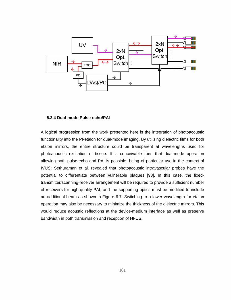
101
6.2.4 Dual-mode Pulse-echo/PAI
A logical progression from the work presented here is the integration of photoacoustic
functionality into the PI-etalon for dual-mode imaging. By utilizing dielectric films for both
etalon mirrors, the entire structure could be transparent at wavelengths used for
photoacoustic excitation of tissue. It is conceivable then that dual-mode operation
allowing both pulse-echo and PAI is possible, being of particular use in the context of
IVUS; Sethuraman et al. revealed that photoacoustic intravascular probes have the
potential to differentiate between vulnerable plaques [98]. In this case, the fixed-
transmitter/scanning-receiver arrangement will be required to provide a sufficient number
of receivers for high quality PAI, and the supporting optics must be modified to include
an additional beam as shown in Figure 6.7. Switching to a lower wavelength for etalon
operation may also be necessary to minimize the thickness of the dielectric mirrors. This
would reduce acoustic reflections at the device-medium interface as well as preserve
bandwidth in both transmission and reception of HFUS.
Figure 6.6. Concept for an all fiber optic imaging system of a fiber PI-etalon array (WDM: wavelength-divisible multiplexer).

Figure 6.7. Potential optical system for dual(PA: photoacoustic source
102
Potential optical system for dual-mode pulse-echo/PAI using a PI-(PA: photoacoustic source).
-etalon array

103
Bibliography
[1] D. F. van Wijk, A. C. Strang, R. Duivenvoorden, D. F. Enklaar, R. J. van der Geest, J. J. Kastelein, E. de Groot, S. G. Stroes, and A. J. Nederveen, “Increasing spatial resolution of 3T MRI scanning improves reproducibility of carotid arterial wall dimensions measurements,” Magn. Reson. Mater. Phy., vol. 27, pp 219-226, 2014. [2] Y. Zhao, E. Brun, P. Coan, Z. Huang, A. Sztrokay, P. C. Diemoz, S. Liebhardt, A. Mittone, S. Gasilov, J. Miao, and A. Bravin, “High-resolution, low-dose phase contrast X-ray tomography for 3D diagnosis of human breast cancers,” Proc. Nat. Acad. Sci, vol. 109, no. 45, pp. 18290-18294, 2012. [3] J. T. Bushberg, J. A. Seibert, E. M. Leidholdt, and J. M. Boone, The Essential Physics of Medical Imaging, Philadelphia, PA: Lippincott Williams & Wilkins, 2012, pp. 15. [4] F. S. Foster, C.J. Pavlin, K. A. Harasiewicz, D. A. Christopher, and D. H. Turnbull, “Advances in ultrasound biomicroscopy,” Ultrasound Med. & Biol., vol. 26, no. 1, pp. 1-27, 2000. [5] D. A. Knapik, B. Starkoski, C.J. Pavlin, and F.S. Foster, “A 100-200 MHz ultrasound biomicroscope,” IEEE Trans. Ultrason. Ferrorelectr. Freq. Control, vol. 47, no. 5, pp. 1540-1549, 2000. [6] X. Li, W. Wu, Y. Chung, W. Y. Shih, W. Shih, Q. Zhou, K. K. Shung, “80-MHz intravascular ultrasound transducer using PMN-PT free-standing film, IEEE Trans. Ultrason. Ferroelectr. Freq. Control, vol. 58, no. 11, Nov. 2011. [7] X. Li, W. Wei, Q. Zhou, K. K. Shung, and Z. Chen, “Intravascular photoacoustic imaging at 35 and 80 MHz,” J. Biomed. Optics, vol. 17, no. 10, pp. 106005-1, 2012. [8] C. K. Lee and P. J. Benkeser, “Investigation of a forward-looking IVUS imaging transducer,” in Proc. IEEE Ultrasonics Symp., 1991, pp. 691-694. [9] L. Gatzoulis, R. J. Watson, L. B. Jordan, S. D. Pye, T. Anderson, N. Uren, D. M. Salter, K. A. Fox, and W. N. McDicken, “Three-dimensional forward-viewing intravascular ultrasound imaging of human arteries in vitro,” Ultrasound Med. Biol., vol. 27, no. 7, pp. 969-982, 2001. [10] B. J. Kimura, V. Bhargava, W. Palinski, R. J. Russo, and A. N. DeMaria, “Distortion of intravascular ultrasound images because of nonuniform angular velocity of mechanical-type transducers,” Amer. Heart J., vol. 132, no. 2, pp. 328-336, Aug. 1996. [11] M. O’Donnell, M. J. Eberle, D. N. Stephens, J. L. Litzza, K. S. Vicente, and B. M. Shapo, “Synthetic Phased Arrays for Intraluminal Imaging of Coronary Arteries,” IEEE Trans. Ultrason. Ferroelectr. Freq. Control, vol. 44, no. 3, pp. 714-721, May 1997. [12] G. Gurun, C. Tekes, J. Zahorian, T. Xu, S. Satir, M. Karaman, J. Hasler, and F. L. Degertekin, “Single-chip CMUT-on-CMOS front-end system for real-time volumetric IVUS and ICE imaging,” IEEE Trans. Ultrason. Ferroelectr. Freq. Control, vol. 61, no. 2, Feb. 2014. [13] A. Nikoozadeh, I.O. Wygant, D. Lin, O. Oralkan, A. S. Ergun, D. N. Stephens, K. E. Thomenius, A. M. Dentigner, D. Wildes, G. Akopyan, K. Shivkumar, A. Mahajan, D. J. Sahn, and B. T. Khuri-Yakub, “Forward-looking intracardiac ultrasound imaging using a 1-D CMUT array

104
integrated with custom front-end electronics,” IEEE Trans. Ultrason. Ferroelectr. Freq. Control, vol. 55, no. 12, Dec. 2008. [14] J. Hamilton, T. Buma, M. Spisar, and M. O’Donnell, “High frequency optoacoustic arrays using etalon detection,” IEEE Trans. Ultrason. Ferroelectr. Freq. Control, vol. 47, pp. 160–169, Jan. 2000. [15] K. P. Köstli and P. C. Beard, “Two-dimensional photoacoustic imaging by use of Fourier-transform image reconstruction and a detector with an anisotropic response,” Appl. Opt., vol. 42, no. 10, pp. 1899–1908, 2003. [16] S. Ashkenazi, Y. Hou, T. Buma, and M. O’Donnell, “Optoacoustic imaging using thin polymer etalon,” Appl. Phys. Lett., vol. 86, no. 13, art. no. 134102, 2005. [17] C. Sheaff and S. Ashkenazi, “A fiber optic optoacoustic ultrasound sensor for photoacoustic endoscopy,” in Proc. IEEE Ultrasonics Symp., 2010, pp. 2135-2138. [18] L.V. Wang, Photoacoustic Imaging and Spectroscopy, Boca Raton, FL: CRC, 2009, pp. 223-238. [19] P. C. Beard, F. Perennes, and T. N. Mills, "Transduction mechanisms of the Fabry-Perot polymer film sensing concept for wideband ultrasound detection," IEEE Trans. Ultrason., Ferroelect., Freq. Contr., vol. 46, pp. 1575-1582, Nov. 1999. [20] R. M. White, “Generation of elastic waves by transient surface heating,” J. Appl. Phys., vol. 34, no. 12, pp. 3559-3567, 1963. [21] R. J. von Gutfeld and R. L. Melcher, “20 MHz acoustic waves from pulsed thermoelastic expansions of constrained surfaces,” Appl. Phys. Lett., vol. 30, art. no. 257, 1977. [22] A. M. Aindow, R. J. Dewhurst, D. A. Hutchins, and S. B. Palmer, “Laser-generated ultrasonic pulses at free metal surfaces,” J. Acoust. Soc. Am., vol. 69, no. 2, pp. 449-455, 1981. [23] S. Fassbender, B. Hoffmann, and W. Arnold, “Efficient generation of acoustic pressure waves by short laser pulses,” Mat. Sci. Eng. A, vol. 122, no. 1, pp. 37-41, 1989. [24] X. Wang and X. Xu, “Thermoelastic wave induced by pulsed laser heating,” Appl. Phys. A, vol. 73, pp. 107-114, 2001. [25] B. R. Tittmann, R. S. Linebarger, and R. C. Addison Jr., “Laser-based ultrasonics on Gr/epoxy composite,” J. Nondestr. Eval., vol. 9, no. 4, pp. 229-238, 1990. [26] E. Biagi, F. Margheri, and D. Menichelli, “Efficient laser-ultrasound generation by using heavily absorbing films as targets, “ IEEE Trans. Ultrason., Ferroelect., Freq. Contr., vol. 48, pp. 1669-1680, Nov. 2001. [27] T. Buma, M. Spisar, and M. O’Donnell, “High-frequency ultrasound array element using thermoelastic expansion in an elastomeric film,” Appl. Phys. Lett., vol. 79, art. no. 548, 2001. [28] T. Buma, M. Spisar, and M. O’Donnel, “A high-frequency, 2-D array element using thermoelastic expasion in PDMS,” IEEE Trans. Ultrason., Ferroelect., Freq. Contr., vol. 50, pp. 1161-1176, Sep. 2003.

105
[29] Y. Hou, J. Kim, S. Ashkenazi, M. O’Donnell, and J. Guo, “Optical generation of high frequency ultrasound using two-dimensional gold nanostructure,” Appl. Phys. Lett., vol. 89, art. no. 093901, 2006. [30] H. W. Baac, J. G. Ok, H. J. Park, T. Ling, S. Chen, A. J. Hart, and L. J. Guo, “Carbon nanotube composite optoacoustic transmitters for strong and high frequency ultrasound generation,” Appl. Phys. Lett., vol. 97, art. no. 234104, 2010. [31] Y. Hou, J. S. Kim, S. Ashkenazi, S. W. Huang, L. J. Guo, and M. O’Donnell, "Broadband all-optical ultrasound transducers," Appl. Phys. Lett., vol. 91, art. no. 073507, 2007. [32] Y. Hou, J. S. Kim, S. W. Huang, S. Ashkenazi, L. J. Guo, and M. O'Donnell. “Characterization of a broadband all-optical ultrasound transducer-from optical and acoustical properties to imaging,” IEEE Trans. Ultrason., Ferroelect., Freq. Contr., vol. 55, pp. 1867-1877, Aug. 2008. [33] Y. Hou, S. Ashkenazi, S. W. Huang, and M. O'Donnell. “An integrated optoacoustic transducer combining etalon and black PDMS structures,” IEEE Trans. Ultrason., Ferroelect., Freq. Contr., vol. 55, pp. 2719-2725, Dec. 2008. [34] C. Sheaff and S. Ashkenazi, “A polyimide-etalon thin film structure for all-optical high-frequency ultrasound transduction,” IEEE Trans. Ultrason., Ferroelect., Freq. Contr., vol. 59, no. 10, pp. 2254-2261, Oct. 2012. [35] L. V. Wang, Photoacoustic Imaging and Spectroscopy, Boca Raton, FL: CRC, 2009, pp. 3-17. [36] L. V. Wang and H. Wu, Biomedical Optics: Principles and Imaging, Hoboken, NJ: Wiley, 2007, pp. 283-319. [37] Q. Shan, A. Kuhn, P.A. Payne, and R.J. Dewhurst, “Characterization of laser-ultrasound signals from an optical layer within a transparent fluid,” Ultrasonics, vol. 34, no. 6, pp. 629-639, 1996. [38] R. H. French, J. M. Rodriguez-Parada, M. K. Yang, R. A. Derryberry, M. F. Lemon, M. J. Brown, C. R. Haeger, S. L. Samuels, E. C. Romano, and R. E. Richardson, “Optical properties of materials for concentrator photovoltaic systems,” Photovolt. Spec. Conf., pp. 394-399, 2009. [39] C. Sheaff and S. Ashkenazi, “Characterization of an improved polyimide-etalon all-optical transducer for high resolution imaging,” IEEE Trans. Ultrason., Ferroelect., Freq. Contr., vol. 61, no. 7, pp. 1223-1232, Jul. 2014. [40] J. Chalupský, J. Krzywinski, L. Juha, V. Hájková, J. Cihelka, T. Burian, L. Vysín, J. Gaudin, A. Gleeson, M. Jurek, A. R. Khorsand, D. Klinger, H. Wabnitz, R. Sobierajski, M. Störmer, K. Tiedtke, and S. Toleikis, “Spot size characterization of focused non-Gaussian x-ray laser beams,” Opt. Exp., vol. 18, no. 26, Dec. 2010. [41] B. T. Cox and P. C. Beard, “The frequency-dependent directivity of a planar Fabry-Perot polymer film ultrasound sensor,” IEEE Trans. Ultrason., Ferroelect., Freq. Contr., vol. 54, no. 2, Feb. 2007.

106
[42] Ö. Oralkan, B. Bayram, G. G. Yaralioglu, A. S. Ergun, M. Kupnik, D. T. Yeh, I. O. Wygant, and B. T. Khuri-Yakub, “Experimental characterization of collapse-mode CMUT operation,” IEEE Trans. Ultrason. Ferroelectr. Freq. Contr., vol. 53, no. 8, pp. 1513–1523, Aug. 2006. [43] I. O. Wygant, “A comparison of CMUTs and piezoelectric transducer elements for 2D medical imaging based on conventional simulation models,” in Proc. IEEE Ultrasonics Symp., 2011, pp. 100–103. [44] M. Kalms, S. Hellmers, P. Huke, and R. B. Bergmann, “Beam shaping using liquid crystal-on-silicon spatial light modulators for laser ultrasound generation,” Optical Eng., vol. 53, no. 4, pp. 044110-1/-6, Apr. 2014. [45] K. Piglmayer, E. Arenholz, C. Ortwein, N. Arnold, and D. Bäuerle, “Single-pulse ultraviolet laser-induced surface modification and ablation of polyimide,” Appl. Phys. Lett., vol. 73, no. 6, pp. 847-849, Aug. 1998. [46] W. Yung, J. S. Lui, H. C. Man, and T. M. Yue, “355 nm Nd:YAG laser ablation of polyimide and its thermal effect,” J. Mat. Proc. Tech., vol. 101, no. 1-3, pp. 306-311, Apr. 2000. [47] E. Z. Zhang and P. C. Beard, “A miniature all-optical photoacoustic imaging probe,” in Proc. SPIE, 2011, vol. 7899, no. 78991F. [48] M. A. Tadayon, M. E. Baylor, and S. Ashkenazi, “Polymer Waveguide Fabry-Perot Resonator for High-Frequency Ultrasound Detection,” IEEE Trans. Ultrason. Ferroelectr. Freq. Contr., Vol. 61 (2014), No.12. [49] R. Cobbold, Foundations of Biomedical Ultrasound, New York, NY: Oxford, 2007, pp. 187. [50] J. Jensen, S.I. Nikolov, K.L. Gammelmark, M.H. Pederson, “Synthetic aperture ultrasound imaging,” Ultrasonics, Vol. 44, pp. e5-e15, 2006. [51] B. Furlong and S. Motakef, “Scanning lenses and systems,” CVI + Melles Griot. [52] K. Nagai, “A new synthetic-aperture focusing method for ultrasonic B-scan imaging by the fourier transform,” IEEE Trans. Ultrason. Ferroelectr. Freq. Contr., vol. 32, no. 4, pp. 531–536, Jul. 1985. [53] C. Hoelen, F. De Mul, R. Pongers, and A. Dekker, "Three-dimensional photoacoustic imaging of blood vessels in tissue," Opt. Lett., vol. 23, pp. 648-650, 1998. [54] X. Wang, Y. Pang, G. Ku, X. Xie, G. Stoica and L. V. Wang, "Noninvasive laser-induced photoacoustic tomography for structural and functional in vivo imaging of the brain," Nat. Biotechnol., vol. 21, pp. 803-806, 2003. [55] E. Z. Zhang, J. Laufer, and P. Beard, "Three dimensional photoacoustic imaging of vascular anatomy in small animals using an optical detection system," in Proc. of SPIE Vol, 2007, pp. 64370S-1. [56] H. F. Zhang, K. Maslov, G. Stoica, and L. V. Wang, "Functional photoacoustic microscopy for high-resolution and noninvasive in vivo imaging," Nat. Biotechnol., vol. 24, pp. 848-851, 2006. [57] J. Folkman, E. Merler, C. Abernathy and G. Williams, "Isolation of a tumor factor responsible for angiogenesis," J. Exp. Med., vol. 133, pp. 275, 1971.

107
[58] J. Holash, P. Maisonpierre, D. Compton, P. Boland, C. Alexander, D. Zagzag, G. Yancopoulos and S. Wiegand, "Vessel cooption, regression, and growth in tumors mediated by angiopoietins and VEGF," Science, vol. 284, pp. 1994, 1999. [59] C. G. Willett, Y. Boucher, E. di Tomaso, D. G. Duda, L. L. Munn, R. T. Tong, D. C. Chung, D. V. Sahani, S. P. Kalva and S. V. Kozin, "Direct evidence that the VEGF-specific antibody bevacizumab has antivascular effects in human rectal cancer," Nat. Med., vol. 10, pp. 145-147, 2004. [60] D. M. McDonald and P. L. Choyke, "Imaging of angiogenesis: from microscope to clinic," Nat. Med., vol. 9, pp. 713-725, 2003. [61] M. Hockel, K. Schlenger, B. Aral, M. Mitze, U. Schaffer and P. Vaupel, "Association between tumor hypoxia and malignant progression in advanced cancer of the uterine cervix," Cancer Res., vol. 56, pp. 4509, 1996. [62] M. Quintero, N. Mackenzie and P. Brennan, "Hypoxia-inducible factor 1 (HIF-1) in cancer," Euro. J. Surg.l Onc., vol. 30, pp. 465-468, 2004. [63] L. B. Harrison, M. Chadha, R. J. Hill, K. Hu and D. Shasha, "Impact of tumor hypoxia and anemia on radiation therapy outcomes," The Oncologist, vol. 7, pp. 492, 2002. [64] K. A. Krohn, J. M. Link and R. P. Mason, "Molecular imaging of hypoxia," J. Nuc. Med., vol. 49, pp. 129S, 2008. [65] S. Ashkenazi, S. W. Huang, T. Horvath, Y. E. L. Koo and R. Kopelman, "Photoacoustic probing of fluorophore excited state lifetime with application to oxygen sensing," J. Biomed. Opt., vol. 13, pp. 034023, 2008. [66] S. Ashkenazi, “Photoacoustic lifetime imaging of dissolved oxygen using methylene blue,” J. Biomed. Opt., vol. 15, no. 4, pp. 040501, 2010. [67] J. M. Yang, K. Maslov, H. C. Yang, Q. Zhou, K. K. Shung and L. V. Wang, "Photoacoustic endoscopy," Opt. Lett., vol. 34, pp. 1591-1593, 2009. [68] J. M. Yang, K. Maslov, R. Chen, H. C. Yang, Q. Zhou, K. K. Shung and L. V. Wang, "Volumetric photoacoustic endoscopy of internal organs: A phantom and in situ study," in Proceedings of SPIE, 2010, pp. 75640D. [69] J. J. Alcoz, C. Lee and H. Taylor, "Embedded fiber-optic Fabry-Perot ultrasound sensor," IEEE Trans. Ultrason. Ferroelectr. Freq. Contr, vol. 37, pp. 302-306, 1990. [70] P. Beard and T. Mills, "Extrinsic optical-fiber ultrasound sensor using a thin polymer film as a low-finesse Fabry-Perot interferometer," Appl. Opt., vol. 35, pp. 663-675, 1996. [71] P. C. Beard, A. M. Hurrell and T. N. Mills, "Characterization of a polymer film optical fiber hydrophone for use in the range 1 to 20 MHz: A comparison with PVDF needle and membrane hydrophones," IEEE Trans. Ultrason. Ferroelectr. Freq. Contr., vol. 47, pp. 256-264, 2000. [72] P. Morris, A. Hurrell, A. Shaw, E. Zhang and P. Beard, "A Fabry–Pérot fiber-optic ultrasonic hydrophone for the simultaneous measurement of temperature and acoustic pressure," J. Acoust. Soc. Am., vol. 125, pp. 3611, 2009.
108
[73] E. Biagi, S. Fontani, F. Francini, L. Masotti, and M. Pieraccini. "Photoacoustic generation: all-optical fibre transducers," In Proc. IEEE Ultrasonics Symp., 1996, pp. 921-924. [74] P. A. Fomitchov, A. K. Kromine, and S. Krishnaswamy. "Photoacoustic probes for nondestructive testing and biomedical applications." Appl. Opt., vol. 41, no. 22, pp. 4451-4459, 2002. [75] L. Belsito, E. Vannacci, F. Mancarella, M. Ferri, G. P. Veronese, E. Biagi, and A. Roncaglia, "Fabrication of fiber-optic broadband ultrasound emitters by micro-opto-mechanical technology," J. of Micromech. Microeng., vol. 24, no. 8, pp. 085003, 2014. [76] R. J. Colchester, C. A. Mosse, D. S. Bhachu, J. C. Bear, C. J. Carmalt, I. Papakonstantinou, and A. E. Desjardins, “Laser-generated ultrasound with optical fibres using functionalised carbon nanotube composite coatings,” Appl. Phys. Lett., vol. 104, no. 17, pp. 173502, 2014. [77] http://press.thorlabs.com/articles/video-rate-scanning-confocal-microscopy-and-microendoscopy/protocol/ (Video-rate Scanning Confocal Microscopy and Microendoscopy). [78] http://www.ceramoptec.com/filephotos/pdf/OptranUVWF.pdf (CeramOptec Optran UV, Optran WF). [79] Kubono, Atsushi, and Norimasa Okui. "Polymer thin films prepared by vapor deposition." Prog. Polymer Sci., vol. 19, no. 3, pp. 389-438, 1994. [80] V. Malba, V. Liberman, and A. F. Bernhardt. "Vapor deposition polymerization of polyimide for microelectronic applications," J. Vacuum Sci. Tech. A, vol. 15, no. 3, pp. 844-849, 1997. [81] J. P. González, A. Lamure, and F. Senocq, "Polyimide (PI) films by chemical vapor deposition (CVD): Novel design, experiments and characterization," Surf. Coat. Tech., vol. 201, no. 22, pp. 9437-9441, 2007. [82] S. Q. Tran, "Method of forming a composite coating with particle materials that are readily dispersed in a sprayable polyimide solution," U.S. Patent No. 5,753,306. 19 May 1998. [83] S. Q. Tran, "Method of forming a hot film sensor system on a model." U.S. Patent No. 5,789,020. 4 Aug. 1998. [84] D. Vak, S. S. Kim, J. Jo, S. H. Oh, S. I. Na, J. Kim, and D. Y. Kim, “Fabrication of organic bulk heterojunction solar cells by a spray deposition method for low-cost power generation,” Appl. Phys. Lett., vol. 91, no. 8, pp. 081102, 2007. [85] R. Green, A. Morfa, A. J. Ferguson, N. Kopidakis, G. Rumbles, and S. E. Shaheen, "Performance of bulk heterojunction photovoltaic devices prepared by airbrush spray deposition," Appl. Phys. Lett., vol. 92, no. 3, pp. 033301, 2008. [86] C. Girotto, B. P. Rand, J. Genoe, and P. Heremans, "Exploring spray coating as a deposition technique for the fabrication of solution-processed solar cells," Sol. Ener. Mat. Solar Cells, vol. 93, no. 4, pp. 454-458, 2009. [87] G. Susanna, L. Salamandra, T. M. Brown, A. Di Carlo, F. Brunetti, and A. Reale, "Airbrush spray-coating of polymer bulk-heterojunction solar cells," Sol. Ener. Mat. Sol. Cells, vol. 95, no. 7, pp. 1775-1778, 2011.

109
[88] B. K. Yu, D. Vak, J. Jo, S. Na, S. S. Kim, M. K. Kim, and D. Y. Kim, "Factors to be considered in bulk heterojunction polymer solar cells fabricated by the spray process." IEEE J. Sel. Top. Quan. Elec., vol. 16, no. 6, pp. 1838-1846, 2010. [89] M. Noebels, R. E. Cross, D. A. Evans, and C. E. Finlayson, "Characterization of spray-coating methods for conjugated polymer blend thin films," J. Mat. Sci., vol. 49, no. 12, pp. 4279-4287, 2014. [90] http://www.thorlabs.us/newgrouppage9.cfm?objectgroup_id=8013 (5-axis Kinematic Mount). [91] T. Shiina, K. Noguchi, and T. Fukuchi, "Polarization-independent optical circulator for high accuracy Faraday depolarization lidar," Appl. Opt., vol. 51, no. 7, pp. 898-904, 2012. [92] J. Li, A. Taylor, I. Papakonstantinou, E. Zhang, and P. Beard, "Highly sensitive optical microresonator sensors for photoacoustic imaging," In Proc. SPIE BiOS, 2014, pp. 89430C-89430C. [93] P. C. Beard and T. N. Mills, "Miniature optical fibre ultrasonic hydrophone using a Fabry-Perot polymer film interferometer," Elec. Lett., vol. 33, no. 9, pp. 801-803, 1997. [94] F. Pérennès, P. C. Beard, and T. N. Mills, "Analysis of a low-finesse Fabry-Perot sensing interferometer illuminated by a multimode optical fiber," Appl. Opt., vol. 38, no. 34, pp. 7026-7034, 1999. [95] M. Lamont and P. C. Beard, "2D imaging of ultrasound fields using CCD array to map output of Fabry-Perot polymer film sensor," Elec. Lett., vol. 42, no. 3, pp. 187-189, 2006. [96] A. Meyer, S. Gspan, S. Bernet, and M. Ritsch-Marte, “Binary optoacoustic holography with a spatial light modulator,” J. Appl. Phys., vol. 96, no. 10, pp. 5886-5891, 2004. [97] M. D. Brown, T. J. Allen, B. T. Cox, and B. E. Treeby. "Control of optically generated ultrasound fields using binary amplitude holograms," In IEEE Ultrasonics Symp., 2014, pp. 1037-1040. [98] S. Sethuraman, J. H. Amirian, S. H. Litovsky, R. W. Smalling, and S. Y. Emelianov, “Spectroscopic intravascular photoacoustic imaging to differentiate atherosclerotic plaques,” Opt. Exp., vol. 16, no. 5, pp. 3362-3367, Feb. 2008.