all-epitaxially orientation-patterned …nlo.stanford.edu/system/...thesis_december_2001.pdf · new...
TRANSCRIPT

ALL-EPITAXIALLY ORIENTATION-PATTERNED SEMICONDUCTORS FOR
NONLINEAR OPTICAL FREQUENCY CONVERSION
A DISSERTATION
SUBMITTED TO THE DEPARTMENT OF APPLIED PHYSICS
AND THE COMMITTEE ON GRADUATE STUDIES
OF STANFORD UNIVERSITY
IN PARTIAL FULFILLMENT OF THE REQUIREMENTS
FOR THE DEGREE OF
DOCTOR OF PHILOSOPHY
Loren Alan Eyres
December 2001

ii
© Copyright by Loren Alan Eyres 2002
All Rights Reserved

iii
I certify that I have read this dissertation and that, in my opinion, it is fully adequate in
scope and quality as a dissertation for the degree of Doctor of Philosopy.
Martin M. Fejer, Principal Advisor
I certify that I have read this dissertation and that, in my opinion, it is fully adequate in
scope and quality as a dissertation for the degree of Doctor of Philosopy.
James S. Harris
I certify that I have read this dissertation and that, in my opinion, it is fully adequate in
scope and quality as a dissertation for the degree of Doctor of Philosopy.
Robert L. Byer
Approved for the University Committee on Graduate Studies:

iv
Abstract
Nonlinear optical frequency conversion is an important technique for generation of mid-
IR radiation from well-developed near-IR pumps like diode lasers and diode-pumped solid-state
lasers. Zincblende semiconductor materials have excellent characteristics for optical frequency
conversion including large nonlinearities and transparency through the mid-IR, but the absence of
birefringence for phasematching has limited their application. Quasiphasematching provides an
alternative solution to this phasematching problem, but requires techniques for inducing a modula-
tion in the nonlinear susceptibility along the crystal. In this work we have developed all-epitaxial
fabrication techniques for orientation-patterned semiconductor materials and have demonstrated
that the resulting devices show excellent promise for mid-IR frequency conversion.
The two step fabrication technique requires making a template with the proper orientation
pattern, which then serves as a substrate for orientation-patterned epitaxial growth. The template
fabrication process utilizes polar-on-nonpolar molecular beam epitaxy (MBE) of a GaAs/Ge/GaAs
heterostructure to achieve an epitaxial crystal inversion, after which the template is completed by a
combination of photolithography and selective chemical etching. Orientation-patterned
Al
x
Ga
1-x
As films grown on these templates exhibit ideal vertical antiphase domain propagation.
Periods were demonstrated sufficient for quasiphasematching any collinear frequency mixing
interaction in the transparency range of Al
x
Ga
1-x
As. Orientation-patterned Al
x
Ga
1-x
As waveguid-
ing structures were fabricated and utilized for harmonic generation of 1.55 µm laser radiation. The
conversion efficiencies in these waveguide devices were limited by high modal propagation losses
at both fundamental and harmonic wavelengths.
Thin GaAs orientation-patterned films were also used as templates for growth of much
thicker (100s of µm) GaAs films by the hydride vapor phase epitaxy (HVPE) technique for bulk-
focused frequency conversion. The antiphase boundaries were again observed to propagate verti-
cally through the GaAs film with aspect ratios > 15:1. Periods sufficient to quasiphasematch para-
metric amplification using pump lasers of wavelength longer than 1.5 µm were demonstrated and
excellent optical transmission was observed at both near-IR and mid-IR wavelengths. Frequency
doubling of confocally-focused CO
2
laser radiation was performed in such an orientation-pat-
terned film with efficiency close to theoretical.

v
Acknowledgements
Early in my Stanford career, a frequent visitor to the Byer-Fejer noontime group meeting
said, in some superposition of seriousness and jest, that “. . .the meaning of life is to stay around
Stanford as long as possible”. The reasons for this attraction are obvious: the challenging intel-
lectual environment, exceedingly talented and motivated colleagues, excellent resources, and
many diverse opportunities. Though remaining as long as possible wasn’t my intention, I have
accumulated many enjoyable experiences and learned a great deal, both about physics and about
life in general. I am grateful to all the people who have been a part of that; I am a wiser and better
person as a result. In research, as in life, any large and meaningful project requires much help
from others to be successful. Many more people played a part than I can hope to mention here.
My acknowledgements must begin with my advisor, Prof. Marty Fejer, who gave me the
freedom to tackle a large project and supported me over the long time it took to complete it. His
almost uncanny ability to ask penetrating questions and extract the essential elements of a problem
from his interlocutor’s mind proved invaluable for solving many of the problems we faced along
the way. Prof. Jim Harris played a crucial role with his knowledge of epitaxy and his willingness
to put a germanium source on MBE system II for this project (knowing it would contaminate the
machine for other uses). I thank professor Prof. Bob Byer for his encouragement, especially dur-
ing the bleakest periods of moving the MBE systems. I found it gratifying to hear him acknowl-
edge the difficulties and frustrations of materials research.
Chris Ebert and Thierry Pinguet made possible the success of this project by doing the
MBE growth and taking on lions’ shares of MBE maintenance. Chris invested a great deal of
effort in system modification and exploratory growths before we knew whether the scheme would
work. I greatly enjoyed working with him, whether we were hunched over a RHEED screen look-
ing at surface reconstructions, or setting up a tent somewhere in the Sierra Nevada. Thierry was
somehow able to grow templates for the thick GaAs experiments in spite of myriad MBE prob-
lems. We characterized the first thick, orientation-patterned GaAs films together and discussed the
meaning of life on our way back and forth to Livermore. Patrick Tourreau contributed signifi-
cantly to getting the thick GaAs work underway while simultaneously becoming a fun housemate
and good friend. Thierry, Ofer Levi, Torbjorn Skauli, and Luigi Scaccabarozzi continued to push
the technology forward after I bowed out to write this dissertation and have generated very impres-

vi
sive new results. Many other Harris group members also indirectly supported this project through
their MBE maintenance efforts.
Extended collaboration with Eric Lallier, Loic Becouarn, and Bruno Gerard at Thales
(Thomson-CSF) allowed this project to proceed much faster and further than we could have pro-
pelled it at Stanford alone. Their HVPE GaAs growth capabilities, combined with our templates,
made possible all the thick GaAs results that demonstrate the utility of these materials and now
motivate serious proposals for their commercialization. Tom Kulp and Scott Bisson from Sandia
National Laboratories were also very helpful in pushing this technology forward through experi-
mental collaboration and support.
My fellow students in the Byer-Fejer research group have probably been the most impor-
tant part of making the lab a rewarding place to work. They were always willing to share ideas and
humor, often willing to share equipment, and even occasionally willing to share work. In my first
years I learned from more experienced students; in the later years I was able to reciprocate for a
new generation. Eric Lim, Mike Bortz, Dieter Jundt, Gary Woods, Darwin Serkland, Steven
Yang, and Chris Pohalski all preceded me through the graduate student experience and offered
both models and lots of assistance. In my ultimately ill-fated exploration into wafer bonding I had
Leslie Gordon and Dong Zheng as co-workers, with whom I shared equipment and frustrations. I
remember many enjoyable and productive times with Bob Shine, Greg Miller, Larry Myers, Matt
Husman, Mark Arbore, Bill Tulloch, Peter Byersdorf, Matthew Lawrence, Todd Rutherford, Justin
Mansell, Gena Imeshev, Ming-Hsien Chou, Krishnan Parameswaran, Andy Schober, Jonathan
Kurz, and Rob Batchko. The Ginzton faculty and students were also a large part of making the lab
such a collegial place, whether in the courtyard at lunchtime or late at night in the hallways and
microfabrication lab. I also have to acknowledge the AP entering class of ‘90 for support and dis-
traction during that first long year of problem sets and laser laboratory experiments.
The group administration, including Kellie Koucky, Jackie Bretz, Annie Tran, Jo Major,
and Sandy Bretz, somehow kept everything from falling apart and did their best to promote group
unity using food. Eric Gustafson, Roger Route, and Bob Eckardt were always available for dis-
cussions about technology or life, while also taking care of tedious but important work like bud-
geting and proposal writing so that we as students could concentrate on research. Tom Carver
always had helpful suggestions for dealing with microfabrication problems, as did Larry Randall
for computer networking, machine shop, and automotive problems. Paula Perron and the other
Applied Physics office staff saved me from stereotypically forgetting important deadlines and

vii
incurring associated University fines. The Ginzton front office staff managed administrative
issues we would usually rather avoid. Joe Vrhel and Chris Remen polished many oxide and semi-
conductor crystals for use in experiments. Dr. Mike Kelly helped me operate the XPS system and
interpret the results.
Happily, I didn’t spend the whole time at Stanford working. Singing with the Stanford
Early Music Singers has been a very enjoyable distraction from the frustrations of research, partic-
ularly during long stretches of MBE downtime. Singing 15th century polyphony in the Memorial
Church is an experience no one should miss. Classes and faculty in the French and Italian depart-
ment, particularly involving Rene Girard and Jean-Pierre Dupuy, provided fascinating and existen-
tially challenging intellectual diversions when I could take time away from research. Playing
volleyball with the Ginzton GSB team gave me a good outlet for frustration and taught me a little
about refereeing in a world where some people take things way too seriously. Thanks also to the
friends who got me into swing dancing (especially Leslie Gordon) just in time for the late ‘90s
swing revival in the Bay area.
After sharing a ramshackle house at 519 University Drive with 11 different housemates
over eight years, I now have lots of good friends around the world who share my memories of
leaking water heaters, broken automobiles, stolen bicycles, and occasional sleepwalking incidents.
Thanks to all the friends with whom I have spent time working, playing or reflecting over the last
decade. I feel a special gratitude towards everyone who was supportive during the last grueling
phases of writing this dissertation.
Finally, I am grateful to my family. My brother Dean is my best friend and has always
provided encouragement and a lot of fun whenever we have gotten together. I thank my parents,
Jack and Marge Eyres, for the innumerable things they have given me over the years, including a
life which has been filled with so many opportunities.
The research in this dissertation was supported by the Defense Advanced Research
Projects Agency through the Office of Naval Research under the Center for Nonlinear Optical
Materials (N00014-92-J-1903), by the Army Research Office under contract DAAH04-96-1-0002,
and by the Department of Energy through Sandia National Laboratories under contract SNL4489.

viii
Table of Contents
Abstract
. . . . . . . . . . . . . . . . . . . . . . . . . . . . . . . . . . . . . . . . . . . . . . . . . . . . . . . . . . . . . . . . . . . . . iv
Acknowledgements
. . . . . . . . . . . . . . . . . . . . . . . . . . . . . . . . . . . . . . . . . . . . . . . . . . . . . . . . . . . v
Table of Contents
. . . . . . . . . . . . . . . . . . . . . . . . . . . . . . . . . . . . . . . . . . . . . . . . . . . . . . . . . . . viii
List of Tables
. . . . . . . . . . . . . . . . . . . . . . . . . . . . . . . . . . . . . . . . . . . . . . . . . . . . . . . . . . . . . . . . xi
List of Figures
. . . . . . . . . . . . . . . . . . . . . . . . . . . . . . . . . . . . . . . . . . . . . . . . . . . . . . . . . . . . . . xii
CHAPTER 1: New Materials for Nonlinear Optical Frequency Conversion
. . . . . . . . . 1
1.1 Introduction
. . . . . . . . . . . . . . . . . . . . . . . . . . . . . . . . . . . . . . . . . . . . . . . . . . . .1
1.2 Background
. . . . . . . . . . . . . . . . . . . . . . . . . . . . . . . . . . . . . . . . . . . . . . . . . . . .2
1.2.1 Nonlinear optical frequency conversion
. . . . . . . . . . . . . . . . . . . . . . . . . . . .2
1.2.2 Phasematching and efficiency
. . . . . . . . . . . . . . . . . . . . . . . . . . . . . . . . . . .3
1.2.3 Quasiphasematching
. . . . . . . . . . . . . . . . . . . . . . . . . . . . . . . . . . . . . . . . .4
1.3 Applications
. . . . . . . . . . . . . . . . . . . . . . . . . . . . . . . . . . . . . . . . . . . . . . . . . . . .6
1.3.1 Mid-IR generation
. . . . . . . . . . . . . . . . . . . . . . . . . . . . . . . . . . . . . . . . . . .6
1.3.2 Optical communications
. . . . . . . . . . . . . . . . . . . . . . . . . . . . . . . . . . . . . . .6
1.4 Mid-IR sources
. . . . . . . . . . . . . . . . . . . . . . . . . . . . . . . . . . . . . . . . . . . . . . . . . .7
1.5 Comparison of NLO materials
. . . . . . . . . . . . . . . . . . . . . . . . . . . . . . . . . . . . . . .9
1.6 History of QPM in semiconductors
. . . . . . . . . . . . . . . . . . . . . . . . . . . . . . . . . . .10
1.6.1 Stack of plates
. . . . . . . . . . . . . . . . . . . . . . . . . . . . . . . . . . . . . . . . . . . . .11
1.6.2 Orientation-patterned epitaxial growth
. . . . . . . . . . . . . . . . . . . . . . . . . . .11
1.7 All-epitaxial template fabrication
. . . . . . . . . . . . . . . . . . . . . . . . . . . . . . . . . . . .12
1.8 Dissertation overview
. . . . . . . . . . . . . . . . . . . . . . . . . . . . . . . . . . . . . . . . . . . .13
CHAPTER 2: Theory of Nonlinear Optical Frequency Conversion
. . . . . . . . . . . . . . . . . . 19
2.1 Plane wave frequency conversion
. . . . . . . . . . . . . . . . . . . . . . . . . . . . . . . . . . . .19
2.1.1 Coupled equations
. . . . . . . . . . . . . . . . . . . . . . . . . . . . . . . . . . . . . . . . . .19
2.1.2 Conversion efficiency
. . . . . . . . . . . . . . . . . . . . . . . . . . . . . . . . . . . . . . . .21
2.1.3 Polarization and effective nonlinearity
. . . . . . . . . . . . . . . . . . . . . . . . . . . .22
2.1.4 Quasiphasematching
. . . . . . . . . . . . . . . . . . . . . . . . . . . . . . . . . . . . . . . .25
2.1.5 Attenuation effects
. . . . . . . . . . . . . . . . . . . . . . . . . . . . . . . . . . . . . . . . . .26
2.2 Frequency conversion in waveguides
. . . . . . . . . . . . . . . . . . . . . . . . . . . . . . . . .27
2.2.1 Mode normalization
. . . . . . . . . . . . . . . . . . . . . . . . . . . . . . . . . . . . . . . . .27
2.2.2 Efficiency and effective area
. . . . . . . . . . . . . . . . . . . . . . . . . . . . . . . . . . .29
2.2.3 One-dimensional slab waveguides
. . . . . . . . . . . . . . . . . . . . . . . . . . . . . . .30
2.2.4 Mode overlaps of four-layer planar waveguides
. . . . . . . . . . . . . . . . . . . . .32
2.2.5 Waveguide NLO device predictions
. . . . . . . . . . . . . . . . . . . . . . . . . . . . . .35

ix
2.3 Bulk single-pass NLO CW devices
. . . . . . . . . . . . . . . . . . . . . . . . . . . . . . . . . . 38
2.3.1 Difference frequency generation
. . . . . . . . . . . . . . . . . . . . . . . . . . . . . . . 38
2.3.2 Second harmonic generation
. . . . . . . . . . . . . . . . . . . . . . . . . . . . . . . . . . 40
2.4 Conclusion
. . . . . . . . . . . . . . . . . . . . . . . . . . . . . . . . . . . . . . . . . . . . . . . . . . . 41
CHAPTER 3: All-Epitaxial Fabrication of GaAs Orientation Templates
. . . . . . . . . . . . . . 43
3.1 Introduction
. . . . . . . . . . . . . . . . . . . . . . . . . . . . . . . . . . . . . . . . . . . . . . . . . . . 43
3.1.1 Overview
. . . . . . . . . . . . . . . . . . . . . . . . . . . . . . . . . . . . . . . . . . . . . . . . 44
3.1.2 MBE outline
. . . . . . . . . . . . . . . . . . . . . . . . . . . . . . . . . . . . . . . . . . . . . 48
3.1.3 RHEED
. . . . . . . . . . . . . . . . . . . . . . . . . . . . . . . . . . . . . . . . . . . . . . . . . 49
3.2 Epitaxial inversion: Background
. . . . . . . . . . . . . . . . . . . . . . . . . . . . . . . . . . . . 50
3.2.1 Growth of Ge on GaAs(001)
. . . . . . . . . . . . . . . . . . . . . . . . . . . . . . . . . . 50
3.2.2 Growth of GaAs on Ge(001)
. . . . . . . . . . . . . . . . . . . . . . . . . . . . . . . . . . 52
3.2.3 Growth of GaAs/Ge/GaAs heterostructures
. . . . . . . . . . . . . . . . . . . . . . . 56
3.3 Epitaxial inversion: Experimental
. . . . . . . . . . . . . . . . . . . . . . . . . . . . . . . . . . . 57
3.3.1 Epitaxial inversion strategy
. . . . . . . . . . . . . . . . . . . . . . . . . . . . . . . . . . . 58
3.3.2 Surface smoothing
. . . . . . . . . . . . . . . . . . . . . . . . . . . . . . . . . . . . . . . . . 59
3.3.3 APD size reduction
. . . . . . . . . . . . . . . . . . . . . . . . . . . . . . . . . . . . . . . . . 62
3.3.4 Template recipe
. . . . . . . . . . . . . . . . . . . . . . . . . . . . . . . . . . . . . . . . . . . 64
3.3.5 Further orientation/APB studies
. . . . . . . . . . . . . . . . . . . . . . . . . . . . . . . . 65
3.3.6 Thin buffer exploration
. . . . . . . . . . . . . . . . . . . . . . . . . . . . . . . . . . . . . . 70
3.4 Epitaxial inversion: Discussion
. . . . . . . . . . . . . . . . . . . . . . . . . . . . . . . . . . . . . 71
3.4.1 APD disorder
. . . . . . . . . . . . . . . . . . . . . . . . . . . . . . . . . . . . . . . . . . . . . 71
3.4.2 Orientation
. . . . . . . . . . . . . . . . . . . . . . . . . . . . . . . . . . . . . . . . . . . . . . . 72
3.4.3 Complications from arsenic exposure
. . . . . . . . . . . . . . . . . . . . . . . . . . . . 73
3.4.4 Recommendations
. . . . . . . . . . . . . . . . . . . . . . . . . . . . . . . . . . . . . . . . . 75
3.5 Template etching
. . . . . . . . . . . . . . . . . . . . . . . . . . . . . . . . . . . . . . . . . . . . . . . 76
3.5.1 Lift-off templates
. . . . . . . . . . . . . . . . . . . . . . . . . . . . . . . . . . . . . . . . . . 77
3.5.2 Etch-stop templates
. . . . . . . . . . . . . . . . . . . . . . . . . . . . . . . . . . . . . . . . 79
3.6 MBE regrowth
. . . . . . . . . . . . . . . . . . . . . . . . . . . . . . . . . . . . . . . . . . . . . . . . . 85
3.6.1 Surface preparation
. . . . . . . . . . . . . . . . . . . . . . . . . . . . . . . . . . . . . . . . . 86
3.6.2 Orientation-patterned regrowth
. . . . . . . . . . . . . . . . . . . . . . . . . . . . . . . . 86
3.7 Conclusion
. . . . . . . . . . . . . . . . . . . . . . . . . . . . . . . . . . . . . . . . . . . . . . . . . . . 90
CHAPTER 4: Fabrication and Characterization of Orientation-Patterned Waveguide Devices
. . . . . . . . . . . . . . . . . . . . . . . . . . . . . . . . . . . . . . . . . . . . . . . . 97
4.1 Introduction
. . . . . . . . . . . . . . . . . . . . . . . . . . . . . . . . . . . . . . . . . . . . . . . . . . . 97
4.2 Waveguide Design
. . . . . . . . . . . . . . . . . . . . . . . . . . . . . . . . . . . . . . . . . . . . . 100
4.2.1 Considerations and constraints
. . . . . . . . . . . . . . . . . . . . . . . . . . . . . . . . 100
4.2.2 Finite difference equation (FDE) modelling
. . . . . . . . . . . . . . . . . . . . . . 103
4.3 Orientation-patterned waveguide fabrication
. . . . . . . . . . . . . . . . . . . . . . . . . . 104
4.3.1 MBE regrowth of waveguide structures
. . . . . . . . . . . . . . . . . . . . . . . . . 104
4.3.2 Diffusion-limited wet chemical etching
. . . . . . . . . . . . . . . . . . . . . . . . . 107
4.3.3 Additional fabrication
. . . . . . . . . . . . . . . . . . . . . . . . . . . . . . . . . . . . . . 108

x
4.4 Optical characterization
. . . . . . . . . . . . . . . . . . . . . . . . . . . . . . . . . . . . . . . . . .109
4.4.1 Optical attenuation
. . . . . . . . . . . . . . . . . . . . . . . . . . . . . . . . . . . . . . . .110
4.4.2 Harmonic generation
. . . . . . . . . . . . . . . . . . . . . . . . . . . . . . . . . . . . . . .112
4.5 Discussion
. . . . . . . . . . . . . . . . . . . . . . . . . . . . . . . . . . . . . . . . . . . . . . . . . . .114
4.6 Conclusion
. . . . . . . . . . . . . . . . . . . . . . . . . . . . . . . . . . . . . . . . . . . . . . . . . . .116
CHAPTER 5: Growth and Characterization of Thick Orientation-Patterned GaAs
. . . 123
5.1 Introduction
. . . . . . . . . . . . . . . . . . . . . . . . . . . . . . . . . . . . . . . . . . . . . . . . . .123
5.2 Thick GaAs growth processes
. . . . . . . . . . . . . . . . . . . . . . . . . . . . . . . . . . . . .123
5.2.1 Growth by CL-VPE
. . . . . . . . . . . . . . . . . . . . . . . . . . . . . . . . . . . . . . . .125
5.2.2 Growth by HVPE
. . . . . . . . . . . . . . . . . . . . . . . . . . . . . . . . . . . . . . . . .1265.3 Characterization of thick GaAs films . . . . . . . . . . . . . . . . . . . . . . . . . . . . . . . .128
5.3.1 Grating orientation and domain quality . . . . . . . . . . . . . . . . . . . . . . . . . .1285.3.2 Surface morphology . . . . . . . . . . . . . . . . . . . . . . . . . . . . . . . . . . . . . . .1305.3.3 Domain defects . . . . . . . . . . . . . . . . . . . . . . . . . . . . . . . . . . . . . . . . . . .1325.3.4 Projections for thicker films . . . . . . . . . . . . . . . . . . . . . . . . . . . . . . . . . .135
5.4 Linear optical characterization . . . . . . . . . . . . . . . . . . . . . . . . . . . . . . . . . . . . .1365.5 Nonlinear optical characterization . . . . . . . . . . . . . . . . . . . . . . . . . . . . . . . . . .1395.6 Conclusion . . . . . . . . . . . . . . . . . . . . . . . . . . . . . . . . . . . . . . . . . . . . . . . . . . .141
CHAPTER 6: High Power Operation and Future Devices . . . . . . . . . . . . . . . . . . . . . . . . 145
6.1 Introduction . . . . . . . . . . . . . . . . . . . . . . . . . . . . . . . . . . . . . . . . . . . . . . . . . .1456.2 Constraints on high power operation. . . . . . . . . . . . . . . . . . . . . . . . . . . . . . . . .145
6.2.1 Damage threshold . . . . . . . . . . . . . . . . . . . . . . . . . . . . . . . . . . . . . . . . .1466.2.2 Thermal effects . . . . . . . . . . . . . . . . . . . . . . . . . . . . . . . . . . . . . . . . . . .1466.2.3 Two-photon absorption . . . . . . . . . . . . . . . . . . . . . . . . . . . . . . . . . . . . .148
6.3 Device modeling . . . . . . . . . . . . . . . . . . . . . . . . . . . . . . . . . . . . . . . . . . . . . . .1506.3.1 OPA/OPG . . . . . . . . . . . . . . . . . . . . . . . . . . . . . . . . . . . . . . . . . . . . . . .1516.3.2 OPOs . . . . . . . . . . . . . . . . . . . . . . . . . . . . . . . . . . . . . . . . . . . . . . . . . .154
6.4 Conclusion . . . . . . . . . . . . . . . . . . . . . . . . . . . . . . . . . . . . . . . . . . . . . . . . . . .1596.4 References . . . . . . . . . . . . . . . . . . . . . . . . . . . . . . . . . . . . . . . . . . . . . . . . . . .161
CHAPTER 7: Summary . . . . . . . . . . . . . . . . . . . . . . . . . . . . . . . . . . . . . . . . . . . . . . . . . . . . . . 163
7.1 Accomplishments . . . . . . . . . . . . . . . . . . . . . . . . . . . . . . . . . . . . . . . . . . . . . .1637.1.1 Materials fabrication . . . . . . . . . . . . . . . . . . . . . . . . . . . . . . . . . . . . . . .1637.1.2 Optical characterization . . . . . . . . . . . . . . . . . . . . . . . . . . . . . . . . . . . . .164
7.2 State-of-the-art . . . . . . . . . . . . . . . . . . . . . . . . . . . . . . . . . . . . . . . . . . . . . . . .1647.3 Future work . . . . . . . . . . . . . . . . . . . . . . . . . . . . . . . . . . . . . . . . . . . . . . . . . .165
xi
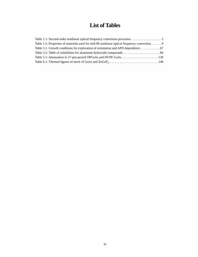
List of Tables
Table 1.1: Second-order nonlinear optical frequency conversion processes. . . . . . . . . . . . . . . . . . . 3
Table 1.2: Properties of materials used for mid-IR nonlinear optical frequency conversion. . . . . . . 9
Table 3.1: Growth conditions for exploration of orientation and APD dependence.. . . . . . . . . . . . 67
Table 3.2: Table of solubilities for aluminum hydroxide compounds . . . . . . . . . . . . . . . . . . . . . . . 84
Table 5.1: Attenuation in 27-µm-period OPGaAs and HVPE GaAs. . . . . . . . . . . . . . . . . . . . . . . 138
Table 6.1: Thermal figures of merit of GaAs and ZnGeP2. . . . . . . . . . . . . . . . . . . . . . . . . . . . . . . 148

xii
List of Figures
Figure 1.1: Impact of phasematching on frequency conversion efficiency. . . . . . . . . . . . . . . . . . . . . . . . . . . 4
Figure 1.2: Domain periods required for quasiphasematching parametric amplification in GaAs for various pump wavelengths.. . . . . . . . . . . . . . . . . . . . . . . . . . . . . . . . . . . . . . . . . . . . . . . . . . . . . . . . . . . . 5
Figure 1.3: Schematic fabrication process for orientation-patterned GaAs. . . . . . . . . . . . . . . . . . . . . . . . . . 13
Figure 2.1: Reference angles used for calculation of GaAs effective nonlinear susceptibilities. . . . . . . . . . 23
Figure 2.2: Four-layer dielectric waveguide structure. . . . . . . . . . . . . . . . . . . . . . . . . . . . . . . . . . . . . . . . . . 31
Figure 2.3: Normalized ω−β diagrams for three and four layer planar waveguides. . . . . . . . . . . . . . . . . . . 32
Figure 2.4: Nondimensional depth parameter as a function of normalized frequency and cladding width. 34
Figure 2.5: Optimal depth parameter as a function of the normalized top cladding width and nondegeneracy.. . . . . . . . . . . . . . . . . . . . . . . . . . . . . . . . . . . . . . . . . . . . . . . . . . . . . . . . . . . . . . 35
Figure 2.6: Schematic diagram of the buried heterostructure used for waveguide device calculations.. . . . 36
Figure 2.7: DFG efficiency for AlGaAs waveguides as a function of core-cladding confinement. . . . . . . . 37
Figure 3.1: Two strategies for obtaining an all-epitaxial, orientation-patterned film.. . . . . . . . . . . . . . . . . . 44
Figure 3.2: GaAs unit cells showing both GaAs phases. . . . . . . . . . . . . . . . . . . . . . . . . . . . . . . . . . . . . . . . 45
Figure 3.3: Gedanken epitaxial inversion with two consecutive atomic layers . . . . . . . . . . . . . . . . . . . . . . 46
Figure 3.4: Schematic illustrating two hypothesized origins of antiphase domains. . . . . . . . . . . . . . . . . . . 54
Figure 3.5: 1-µm-thick GaAs film grown on Ge/GaAs containing very large APDs . . . . . . . . . . . . . . . . . . 61
Figure 3.6: Cross-section through isolated APB with underlying AlAs marker layer. . . . . . . . . . . . . . . . . . 62
Figure 3.7: Anisotropic profiles for photoresist-masked stripes etched into GaAs. . . . . . . . . . . . . . . . . . . . 63
Figure 3.8: Anisotropic etch profiles of 1-µm-thick GaAs layer grown on Ge/GaAs. . . . . . . . . . . . . . . . . . 64
Figure 3.9: Etched sample cross-sections showing APD densities for various wafer misorientations and growth conditions. . . . . . . . . . . . . . . . . . . . . . . . . . . . . . . . . . . . . . . . . . . . . . . . . . . . . . . . . . . . 69
Figure 3.10: Schematic diagram of strained nitride dielectric liftoff structure. . . . . . . . . . . . . . . . . . . . . . . 79
Figure 3.11: Al-O particles on template surface after nominal AlGaAs removal. . . . . . . . . . . . . . . . . . . . . 82
Figure 3.12: XPS depth profiles of GaAs surfaces after etch stop removal.. . . . . . . . . . . . . . . . . . . . . . . . . 83
Figure 3.13: Final template fabrication process showing layer thicknesses. . . . . . . . . . . . . . . . . . . . . . . . . 85
Figure 3.14: SEM micrograph showing disorder at the APB boundary.. . . . . . . . . . . . . . . . . . . . . . . . . . . . 88

xiii
Figure 3.15: Cross-sectional SEM micrograph showing surface with large steps at the APDs. . . . . . . . . . 90
Figure 4.1: Fundamental and harmonic modes of FDE-modelled ridge waveguides. . . . . . . . . . . . . . . . . 103
Figure 4.2: Effective area of etched-rib waveguides for second harmonic generation. . . . . . . . . . . . . . . . 104
Figure 4.3: Stain-etched cross-section of orientation-patterned AlGAs waveguide. . . . . . . . . . . . . . . . . . 106
Figure 4.4: Cleaved facet of orientation-patterned AlGaAs waveguide structure. . . . . . . . . . . . . . . . . . . . 109
Figure 4.5: Attenuation losses across sample for waveguides of varying ridge width. . . . . . . . . . . . . . . . 111
Figure 4.6: Diagram of waveguide harmonic generation experiment. . . . . . . . . . . . . . . . . . . . . . . . . . . . . 113
Figure 4.7: Harmonic generation efficiency as a function of fundamental wavelength for orientation-patterned AlGaAs waveguide. . . . . . . . . . . . . . . . . . . . . . . . . . . . . . . . . . . . . . . . . . . . . . . . . . 114
Figure 5.1: Cross-section of 100-µm-thick GaAs film grown by Cl-VPE. . . . . . . . . . . . . . . . . . . . . . . . . 126
Figure 5.2: Stain-etched 200-µm-thick OPGaAs film with 27-µm domain period . . . . . . . . . . . . . . . . . . 128
Figure 5.3: Grating k-vector alignment relative to the surface misorientation. . . . . . . . . . . . . . . . . . . . . . 129
Figure 5.4: Cross-section of domains with grating k-vector parallel to the misorientation direction. . . . . 130
Figure 5.5: Surface morphology of 27-µm- and 212-µm-period OPGaAs films. . . . . . . . . . . . . . . . . . . . 132
Figure 5.6: Schematic illustrating faceting and growth of adjacent OPGaAs domains. . . . . . . . . . . . . . . 133
Figure 5.7: Top view of 27-µm-period OPGaAs with domain interruptions and pyramidal defects. . . . . 133
Figure 5.8: Schematic of interrupted domain quantities used to determine domain profiles. . . . . . . . . . . 134
Figure 5.9: Domain interruption shape determined from domain annihilation heights . . . . . . . . . . . . . . . 135
Figure 5.10: Cross-section of pyramidal defect on 27 µm domain HVPE film. . . . . . . . . . . . . . . . . . . . . 136
Figure 5.11: Harmonic power as a function of 10.5 µm fundamental power. . . . . . . . . . . . . . . . . . . . . . . 140
Figure 5.12: Conversion efficiency of CO2 laser frequency doubling vs. wavelength. . . . . . . . . . . . . . . . 141
Figure 6.1: TPA coefficient as a function of wavelength for GaAs. . . . . . . . . . . . . . . . . . . . . . . . . . . . . . . 149
Figure 6.2: Theoretical transmission of GaAs as function of two-photon absorption.. . . . . . . . . . . . . . . . 151
Figure 6.3: Conversion efficiency and group walkoff for SHG in OPGaAs. . . . . . . . . . . . . . . . . . . . . . . . 153
Figure 6.4: Parametric gain in OPGaAs pumped at 1.06 µm vs. pump intensity. . . . . . . . . . . . . . . . . . . . 155
Figure 6.5: Threshold fluence of 2-µm-pumped OPO generating an 8 µm idler.. . . . . . . . . . . . . . . . . . . . 156
Figure 6.6: Threshold intensity for 1-µm-pumped OPO vs. GaAs absorption loss. . . . . . . . . . . . . . . . . . 158
Figure 6.7: Threshold intensity for 1.5-µm-pumped OPO vs. GaAs crystal length. . . . . . . . . . . . . . . . . . 159

xiv
1
CHAPTER 1: New Materials for Nonlinear Optical Frequency Conversion
1.1 Introduction
From the initial optical harmonic generation experiments of Franken, et al. in 1961 [1],
nonlinear optical frequency conversion has evolved over the past four decades into both an impor-
tant tool for optical research and an ongoing subject of that research. In the last decade, nonlinear
optical devices such as harmonic generators and parametric oscillators have moved out of the lab-
oratory and become viable commercial products. Examples of this include frequency-doubled
green sources to replace multi-Watt Ar+ ion lasers and optical parametric oscillators generating
mid-IR radiation at the > Watt average power level for military countermeasure applications.
These systems take advantage of recent advances in near-IR, diode-pumped, solid-state laser tech-
nology by converting the radiation from more easily and efficiently generated near-IR wave-
lengths out to the required visible and mid-IR wavelengths. The necessary high performance
frequency conversion devices were enabled by recent advances in the fundamental understanding
of and fabrication of nonlinear materials, in these cases LiBO3, LiNbO3 and ZnGeP2.
Almost without exception, the performance of nonlinear optical devices and the range of
their applications have historically been limited primarily by the available nonlinear optical mate-
rials and their characteristics. Many potentially interesting and useful applications, both scientific
and industrial, await materials having sufficient conversion efficiency, transparency, and power
handling capability. In this situation, the impact of advances in nonlinear optical material devel-
opment is well illustrated by the explosion in device demonstration in the years following the
development of electric-field-poling techniques for lithium niobate and other ferroelectric oxide
materials (see, for example, the Conference on Lasers and Electro-Optics (CLEO) Technical
Digests for 1996-1998). In this case, a material long used for nonlinear optical frequency conver-
sion with birefringent phasematching achieved a qualitative advance in performance through
development of techniques for tailoring the crystal structure on a microscopic scale to enable qua-
siphasematching. One of the highlight devices which resulted from this advance was the demon-
stration of a 93% pump-depleted continuous-wave (CW) singly-resonant optical parametric
oscillator (SRO) generating 3.55 W of 3.25 µm idler radiation from a 1.064 µm pump laser using
periodically-poled lithium niobate (PPLN) by Bosenberg, et al. [2]. Such a device would have
been impossible to build four years earlier for lack of suitable crystals; in fact, the first CW SRO

CHAPTER 1: New Materials for Nonlinear Optical Frequency Conversion
2
was only demonstrated in 1992 [3] and was itself the beneficiary of advances in potassium titanyl
phosphate (KTP) crystal development.
Zincblende semiconductors (GaAs, ZnSe, GaP) have attractive properties for frequency
conversion except for their lack of birefringence. This lack of birefringence for phasematching or
a practical alternative phasematching technique has historically prevented any significant fre-
quency conversion applications. The goal of this dissertation has been to develop microscopic tai-
loring techniques for zincblende semiconductor materials in general and GaAs in particular to
allow quasiphasematching and open up this class of materials for frequency conversion in a man-
ner similar to the ferroelectric oxides. We have succeeded in developing all-epitaxial fabrication
techniques for orientation-patterned gallium arsenide (OPGaAs) using polar-on-nonpolar epitaxy.
Both bulk and waveguide OPGaAs devices have been fabricated and evaluated. Bulk devices per-
form as predicted theoretically with the known material parameters, while the waveguide device
performance is limited by losses which should be reducible through further development of the
fabrication process. These material and optical results confirm the potential of orientation-pat-
terned GaAs and make it look promising for a range of frequency conversion applications.
This chapter provides an introduction to nonlinear optical frequency conversion devices
and their operation, presents their potential applications, and compares the candidate materials for
use in these devices. Following that, it reviews the prior research into quasi-phasematching in
semiconductor materials, outlines the orientation-patterned crystal growth approach taken in this
dissertation, and concludes with an overview of the rest of the dissertation.
1.2 Background
1.2.1 Nonlinear optical frequency conversion
In nonlinear optical frequency conversion, input beams at one or more optical frequencies
interact through the nonlinear polarization in a crystal to generate beams at new frequencies. In
each case, the generated frequency components are constrained by the relationship ,
so that all three frequencies must be present in either the input or output or both. The polarization
induced in a medium can be expanded as a Taylor series in the applied electric field
(1.1)
ω3 ω2 ω1±=
Pi ε0 χ ij1( )
E j χ ijk2( )
E jEk χ ijkl3( )
E jEkEl …+ + +( )=

3
CHAPTER 1: New Materials for Nonlinear Optical Frequency Conversion
with the first term producing the linear effects usually described in terms of the dielectric constant
or the index of the refraction, the next term generating the second-order effects we utilize in this
dissertation, and the third-order term producing effects such as the nonlinear index and four-wave
mixing. The interactions enabled by this second-order susceptibility are shown in Table 1.1
and include second harmonic generation (SHG), sum frequency generation (SFG), difference fre-
quency generation (DFG), and parametric amplification, which is like DFG but with much stron-
ger input beams at the pump than at the signal frequency, which can produce extremely high
amplification at the signal and idler frequencies. Placing a resonant cavity around the parametric
amplifier provides feedback which in combination with the parametric gain results in a parametric
oscillator when the round trip gain exceeds the round trip loss. All of these processes are explored
in more detail in Chapters 2 and 6.
1.2.2 Phasematching and efficiency
In general, this nonlinear conversion process is extremely inefficient unless the problem
of phasematching is solved in some manner. The phasematching problem arises because disper-
sion in the medium causes a phase velocity mismatch between the nonlinear polarization of Equa-
tion (1.1) and the wave it radiates, causing them to walk quickly out of phase and limiting the
coherent interaction length in the material to a distance typically beween a few microns and a few
hundred microns. The effects of phasematching are illustrated in Figure 1.1 using the example of
second harmonic generation. In the unphasematched case, the radiated harmonic power reaches a
maximum after one coherence length, after which the polarization and the radiated wave walk out
of phase and power repeatedly oscillates between fundamental and harmonic. In the perfectly
phasematched, plane-wave, non-depleted pump case, the radiated second harmonic power grows
parabolically with propagation distance in the medium and input fundamental power according to
. (1.2)
process input frequencies output frequencies relationship
SHG
SFG ,
DFG ,
OPA , ,
Table 1.1: Second-order nonlinear optical frequency conversion processes.
χ ijk2( )
ω1 ω2 ω2 ω1 ω1+=
ω1 ω2 ω3 ω3 ω2 ω1+=
ω3 ω2 ω1 ω3 ω2– ω1=
ωpump ωsignal ωidler ωsignal ωpump ωsignal– ωidler=
PSH ηPF2 L2=

CHAPTER 1: New Materials for Nonlinear Optical Frequency Conversion
4
Since nonlinear crystals can have several cm lengths, phasematching can enhance the efficiency
by factors up to (few cm/few µm)2 ~ 108. With phasematching, power conversion efficiencies
around 50% can typically be achieved with SHG and OPO devices. Historically, the problem of
phasematching was solved primarily by utilizing the different refractive indices for differently
polarized waves in birefringent crystals. By choosing the proper combination of input and output
polarizations and the proper propagation angle in the crystal, the phase mis-match could be can-
celled and the parabolic dependence on crystal length realized. Virtually all successful nonlinear
optical frequency conversion until the last decade was achieved using these birefringent phase-
matching techniques. Unfortunately the isotropic optical properties of the zincblende semiconduc-
tor materials such as GaAs preclude birefringent phasematching, so an alternative technique must
be used for these materials.
1.2.3 Quasiphasematching
Quasiphasematching [4] utilizes a periodic modulation of the material parameters to com-
pensate for the phase mismatch. This modulation is usually in the nonlinear susceptibility
and the highest efficiencies are obtained when the modulation alternates sign (+/-). Figure 1.1 also
illustrates the effect of quasiphasematching. After the nonlinear polarization and radiated wave
walk out of phase over one coherence length, the sign of the susceptibility is reversed and the rela-
tive phase between them is reset, allowing the radiation from the following section of the crystal to
add in phase rather than out of phase. With the proper periodic modulation period along the prop-
Figure 1.1: Impact of phasematching on frequency conversion efficiencyas a function of distance through crystal including phasematched, quasi-phasematched,and non-phasematched cases.
0 1 2 3 4
seco
nd h
arm
onic
pow
er (
arbs
)
distance through crystal (coherence lengths)
phasematched
QPM
non-phasematched
+ +- -
χ ijk2( )

5
CHAPTER 1: New Materials for Nonlinear Optical Frequency Conversion
agation direction in the crystal, radiation from the entire crystal adds approximately in phase
resulting in a quasi-parabolic increase in the conversion with crystal length, as shown in
Figure 1.1. Using quasiphasematching techniques, high conversion efficiencies can be obtained
with crystals such as GaAs which have otherwise excellent properties for frequency conversion
but exhibit no birefringence. Figure 1.2 shows the domain periods required for quasiphasematch-
ing parametric amplification in GaAs with various pump wavlengths. For pumping at 2 µm,
coherence lengths (half of the domain period for optimal first-order quasiphasematching) of 30
µm - 45 µm are required, depending on the signal and idler wavelengths, while for 1-µm pumping
the required coherence lengths are 4 µm - 10 µm.
Fabrication of crystals with such a periodic modulation of the nonlinear susceptibility is
nontrivial; the methods which are successful in one material system do not necessarily carry over
into others. Therefore, the key to achieving high-performance, quasi-phasematched frequency
conversion is the invention and development of techniques for fabricating media with modulated
nonlinear susceptibility. This dissertation presents a practical technique for growing GaAs crystals
with a built-in crystal orientation pattern which achieves a periodic sign modulation in the nonlin-
ear susceptibility and makes possible quasiphasematched frequency conversion.
Figure 1.2: Domain periods required for quasiphasematching parametricamplification in GaAs for various pump wavelengths.
0
2
4
6
8
1 0
1 2
0 2 0 4 0 6 0 8 0 100
sign
al a
nd id
ler
wav
elen
gth
(µm
)
domain period (µm)
2.1 µmpump
1.55 µmpump
1.064 µmpump

CHAPTER 1: New Materials for Nonlinear Optical Frequency Conversion
6
1.3 Applications
There are two major categories of application for quasi-phasematched semiconductor fre-
quency conversion materials, mid-IR generation and communication devices.
1.3.1 Mid-IR generation
The mid-IR transparency of GaAs and other zincblende semiconductors makes them
attractive for applications which require wavelengths beyond the ~ 5-µm long-wavelength trans-
parency limit in oxide crystals, or those which require high power at wavelengths longer than
4 µm, where thermal loading can become a limitation in oxide crystals. These applications exist
over a wide range of output power levels and pulse/temporal formats, from low average power
(nW) to high average power (>10 W), from continuous-wave (CW) to ultrashort (fs) pulses. Run-
ning roughly from lowest to highest power, these applications include spectroscopy for fundamen-
tal science and industrial applications, remote sensing for environmental applications, and
sensors/countermeasures for military applications.
Mid-IR spectroscopy applications typically require tunable narrow-linewidth sources with
power levels depending on the context, concentrations, and spectroscopic technique [5-7]. The
mid-IR is attractive for spectroscopy because many molecules have strong vibrational spectra
which allows high-sensitivity measurement. Recently developed cavity ringdown spectroscopy
techniques offer orders of magnitude higher sensitivities due to their extremely long effective path
lengths [8, 9]. Similar techiques can be used for chemical detection, both in industrial processes
and in the ambient environment [10, 11]. The atmospheric transmission windows of 3 µm - 5 µm
and 8 µm - 12 µm restrict remote sensing applications within the mid-IR wavelength range.
Remote sensing of atmospheric or biological chemicals and laser radar require high quality beams
and higher power levels to compensate for power loss in atmospheric propagation and low effi-
ciency collection of scattered radiation from the distant targets [12-14]. Many military counter-
measures applications require multi-Watt average power levels at particular wavelengths to disrupt
missile seekers operating in the mid-IR transmission windows. Many of these applications also
have engineering constraints such as size, weight, and power consumption if they are to be used in
real-world environments rather than in a laboratory.
1.3.2 Optical communications
Semiconductor-based nonlinear optical waveguides also have potential applications in
photonics technology for optical communications. Wavelength conversion will be an essential

7
CHAPTER 1: New Materials for Nonlinear Optical Frequency Conversion
function for future transparent WDM networks and waveguide nonlinear optical frequency con-
version has already demonstrated these functions with excellent efficiencies and linearity. Such
frequency conversion devices fabricated from periodically-poled lithium niobate are capable of
converting a bit stream between wavelength channels at efficiencies of –3dB using only tens of
mW of pump power [15]. The three-frequency-mixing approach has the advantage of being all-
optical, requiring no conversion of photons into electrons, and therefore should easily adapt to
higher bit rates in the future. Such nonlinear waveguide devices have demonstrated simultaneous
multi-channel conversion as well as other functions such as mid-span spectral inversion. Use of
semiconductor waveguides would in principle have several advantages including higher efficien-
cies, which would reduce pump power requirements, and input polarization-independent wave-
length conversion [16], something the current lithium niobate-based devices can’t achieve without
additional device complexity. Since the horizon for implementation in these communication
applications appears further away than for the mid-IR applications, the remainder of this chapter
will focus on the mid-IR, leaving further discussion of communication applications and devices
for chapter 4.
1.4 Mid-IR sources
Some of these requirements for mid-IR sources will be met by non-frequency conversion
devices, but no general solution exists which offers every desired combination of high beam qual-
ity, narrow linewidths, scalable output power, tunability, room-temperature operation, compact
size and robustness. Solid-state lasers operate over limited wavelength ranges around 2 µm
(Ho,Tm:YAG) and 3 µm (Er:YAG). Gas lasers such as CO2 (10 µm) and chemical lasers like HF
and DF also provide sources at specific mid-IR wavelengths. Lead-salt diode lasers can operate in
this range with low output power levels, but only at the cost of cryogenic cooling. The newly-
developed quantum cascade lasers have great promise, having demonstrated emission over the
whole mid-IR, and will certainly solve some subset of problems, but have limitations on power
output and beam quality and generally require tradeoffs between temporal format and cryogenic
cooling.
Meanwhile, near-IR laser diodes and diode-pumped solid-state lasers in the 1.0 - 2.0 µm
wavelength range are well-developed, possessing all of these desirable attributes. For this reason,
mid-IR generation using nonlinear frequency conversion with these versatile near-IR pumps is a
highly appealing strategy for many mid-IR applications provided that the nonlinear optical devices

CHAPTER 1: New Materials for Nonlinear Optical Frequency Conversion
8
achieve sufficient performance, a question which depends primarily on the capabilities of the non-
linear crystals. The most commonly used materials for mid-IR frequency conversion are the chal-
copyrites, including ZnGeP2, AgGaSe2, and AgGaS2, and CdGeAs2, which are presently available
in cm-scale aperatures and multiple cm lengths.
ZnGeP2 has been used effectively for generation over much of the mid-IR spectrum, but
suffers from absorption issues at short wavelength, which constrains pump lasers to operate at
wavelengths > 2.0 µm, and at long wavelength, where phonon-related absorption limits efficien-
cies for wavelengths ≥ 9.0 µm. Perhaps the most impressive device reported is that of Budni,
et al. [17], who demonstrated generation of 10 W combined mid-IR power at 3.67 µm and
4.67 µm from 20 W of pump power with a ZnGeP2 OPO. Optical parametric generation has been
used to produce longer wavelengths out to 11 µm [18], as have recent OPO devices used for spec-
troscopy applications [19].
AgGaSe2 has similarly been useful for generation of radiation through the mid-IR, but is
limited by thermal complications at high power levels due to the low thermal conductivity. Low-
power tunable CW spectroscopy sources around 8 µm have been demonstrated in AgGaSe2 using
near-IR diode lasers as pump sources [20]. OPO experiments by Budni, et al. [21] observed ther-
mal lensing in 2 µm-pumped AgGaSe2 OPOs which limited the conversion efficiency. Moving
away from the unfortunate absorption bands around 2 µm, Chandra, et al. [22] demonstrated a tun-
able 6-14 µm OPO output with 6 ns pulse width at the mJ level for lidar applications. 120 fs
pulses tunable from 4-8 µm were also generated from a sync-pumped AgGaSe2 OPO pumped at
1.57 µm [23]. Tunable output from 8 µm - 12 µm at the mJ level has also been demonstrated by
DFG in a AgGaSe2 crystal of the signal and idler out of a 1-µm-pumped KTP OPO [24].
CdGeAs2 devices have been demonstrated, but the applications are limited by the require-
ment that the pump wavlength be > 3 µm to avoid excess absorption, so it typically must be
pumped by another nonlinear frequency conversion device. Vodopyanov and Schunemann [25]
demonstrated tunable DFG of 7 µm - 20 µm radiation in CdGeAs2 using a 2.8-µm-pumped dou-
ble-pass ZnGeP2 optical parametric generator as a pump source.

9
CHAPTER 1: New Materials for Nonlinear Optical Frequency Conversion
1.5 Comparison of NLO materials
GaAs has excellent characteristics for frequency conversion, as can be seen from a com-
parison with those of the materials mentioned in the previous section. Table 1.2 shows several of
the material properties important for frequency conversion. Material parameters are taken from
several references [26-29]. Attenuation values vary in the references and the ones selected here
are representative of the best production crystals. Three different sets of attenuation data are
shown for GaAs, including typical bulk GaAs wafers, HVPE-grown GaAs films, and orientation-
patterned GaAs with 27 µm period sufficient for phasematching frequency conversion pumped in
the near-IR. The dramatic drop in near-IR attenuation for HVPE GaAs compared to regular bulk
crystal GaAs is due to higher purity and crystal quality. There is some disagreement about the
magnitude of d14 for GaAs, with several authors reporting values consistent with 83 pm/V for 10.6
µm frequency doubling [31], while others observe efficiencies consistent with larger values of
120 pm/V [32] to 150 pm/V [33]. Throughout this dissertation all calculations will assume
90 pm/V value for 10.6 µm frequency doubling scaled by the constant Miller’s delta (CMD) [34]
approximation for the sake of consistency. Results can easily be scaled to adjust as this discrep-
ancy is resolved. The magnitude of d14 for ZnSe is highly uncertain [31, 35]. The walkoff angles
are given for 2 µm pumping of a degenerate OPO.
One can define a material figure of merit proportional to the confocally-focused conver-
sion efficiency in the regime not limited by absorption losses as . GaAs and
material
dij and maximum deff (pm/V)
FOM(pm/V)2
transparencyrange (µm)
thermal conductivity(W/m-K)
attenuation (cm-1)(absorption + scattering)1 µm 2 µm 10 µm
walkoff angle (°)
GaAs 90 (66) 400 0.9 - 12 52 ~ 1 0.01 0.01 0 (QPM)
HVPE-GaAs
0.025
OPGaAs 0.1 0.03*
ZnSe 50 (37) 423 0.5 - 20 18 0.001 0.001 0.0005 0 (QPM)
ZnGeP2 72 522 0.74 - 12 35 1.0 0.09 0.9 0.65
AgGaSe2 34 171 0.7 - 12 1 0.01 0.03 0.01 0.64
CdGeAs2 236 4483 2.3 - 18 4.2 ---- ---- 0.01 ----
AgGaS2 13 29 0.5 - 13 11.5 0.001 0.08 0.6
LiNbO3 27 (17) 67 0.35 - 5 5.6 0.001 0.001 ----
* OPGaAs attenuation value at 1.55 µm from [30]
Table 1.2: Properties of materials used for mid-IR nonlinear optical frequency conversion.
FOM deff n2⁄=

CHAPTER 1: New Materials for Nonlinear Optical Frequency Conversion
10
ZnSe have large FOMs comparable that for ZnGeP2, while exhibiting low optical loss out to
12 µm and 20 µm for GaAs and ZnSe, respectively. This long wavelength transparency and large
FOM, combined with the transparency of GaAs and ZnSe down to 1 µm, should give them signif-
icant advantages over the similar AgGaSe2 and AgGaS2 which are used for long wavelength gen-
eration. In addition, both GaAs and ZnSe have large thermal conductivities which will reduce
dramatically the thermal focusing effects which have complicated AgGaSe2 device operation.
OPGaAs has demonstrated lower attenuation at the three tabulated wavelengths than ZnGeP2. The
attenuation at 1 µm and 2 µm in OPGaAs is likely dominated at present by scattering associated
with the unoptimized orientation-patterned growth, so the thermal performance may actually be
even better. Bulk ZnSe exhibits extremely low attenuation over an extremely wide wavelength
range; it is not clear, however, whether such low losses would be obtainable in orientation-pat-
terned material, as additional attenuation effects might arise. Since they utilize utilize quasiphase-
matching, the zincblende materials don’t suffer from Poynting vector walkoff which restricts
focusing in long crystals and limits the single pass gains. From comparison of the material param-
eters alone, it is reasonable to expect that orientation-patterned GaAs (and ZnSe) could perform as
well or better than the present state-of-the art nonlinear optical materials for mid-IR generation,
particularly in the 9-12 µm wavelength region.
1.6 History of QPM in semiconductors
The attractiveness of zincblende semiconductors and GaAs in particular for frequency
conversion has motivated a number of attempts to achieve practical quasiphasematching. This
section reviews the previous research into quasiphasematching for bulk (focused gaussian beam)
configurations. Research into phasematching techniques such those utilizing quantum wells
which apply only in waveguides devices is covered in chapter 4. Achieving a periodically modu-
lated nonlinear susceptibility in GaAs is somewhat more difficult than accomplishing the same
thing in lithium niobate and other ferroelectrics, since GaAs exhibits no ferroelectricity and there
is no method for inducing a susceptibility modulation into a uniform crystal. Instead, the local
crystal orientation must be modulated periodically, something which can be done using two strate-
gies. In the first, a GaAs crystal is cut into plates, the orientation of every second plate is physi-
cally reversed, and then the whole stack of plates is fused back together. In the second, a template
whose crystallographic orientation is patterned across its surface is fabricated first, after which

11
CHAPTER 1: New Materials for Nonlinear Optical Frequency Conversion
thick or thin films are grown on that template under conditions where the orientation-pattern is
preserved in the growing layers.
1.6.1 Stack of plates
The first successful demonstration of quasiphasematching in GaAs by Szilagyi, et al. [36]
utilized GaAs plates aligned at Brewster’s angle to minimize losses due to Fresnel reflections.
They demonstrated enhancement of nonlinear frequency conversion, but the plates required pre-
cise individual alignment and such a scheme was clearly not mechanically robust. By the addition
of wafer-bonding to the stack-of-plates technique, Gordon, et al. [37] fabricated a robust and
monolithic structure more suitable for real applications. Not only were the individual plates fused
into a single monolithic crystal, but this fusion eliminated the residual Fresnel losses resulting
from air/GaAs interfaces. Using such structures, groups at Stanford and at Thomson-CSF were
able to demonstrate SHG [33, 37], DFG [38, 39], and even an OPO, though the OPO oscillated
only briefly before the crystal damaged [40]. One advantage of this technique is that it enables
crystals of arbitrarily large aperture, easily scaling to two or three inch wafer diameters. There
also are several disadvantages, however. The serial fabrication process scales poorly (since ever
more plates are required) to the long sample lengths desirable for frequency conversion. As the
plate thickness drop significantly below ~ 100 µm, polishing and handling the thin plates becomes
more problematic. Looking back at Figure 1.2, the coherence lengths required for pumping at
wavelengths ≤ 2 µm would be virtually unfabricable using this technique, forcing one to use
higher order QPM at much reduced efficiencies.
One of the few demonstrated alternatives to the stack of plates technique took advantage
of the phase shifts on total internal reflection to phasematch harmonic generation in a single thin
plate of GaAs, ZnSe, and ZnS [41, 42]. This approach followed the original suggestions of
Bloembergen [43]. It is limited by tight tolerances on the precise plate thickness, limited aperture
size, and residual losses due to the repeated total internal reflections from the plate surfaces.
1.6.2 Orientation-patterned epitaxial growth
The second strategy for obtaining an orientation-modulated GaAs crystal is to grow orien-
tation-patterned layers following a previously fabricated template. This technique has several
advantages over the wafer bonding approach. First, the template orientation-pattern dimensions
can be set using photolithography, eliminating tolerances on plate polishing and manageable plate
thicknesses. In principle, narrow periods are equally fabricable as wide periods. The device

CHAPTER 1: New Materials for Nonlinear Optical Frequency Conversion
12
lengths can be extended up to wafer size without difficulty. Many different devices with different
gratings can easily be fabricated in parallel; more complicated non-periodic grating structures,
such as chirped gratings for pulse compression, can be fabricated straightforwardly as well.
Finally, this technique is also compatible with heterostructure waveguide fabrication. The only
intrinsic drawback to this strategy is that the aperture size is limited in one dimension to whatever
thickness can be grown epitaxially.
Historically, there are some precedents for this approach. Angell, et al. [44] invented a
technique for orientation-patterned growth of II-VI ZnSe/ZnTe semiconductor waveguides using
patterned CdTe seeding layers. The devices had on/off modulation of the nonlinear susceptibility
as the ZnSe/ZnTe growth axis alternated between [001] and [111] across the plane of the film.
Unfortunately, the lack of symmetry between the orientations complicated growth of orientation-
patterned layers and resulted in devices with disappointingly high propagation losses. More suc-
cessful orientation-patterning methods were developed by Yoo, et al. employing templates fabri-
cated by wafer-bonding two GaAs wafers using InGaP bonding layers. They grew waveguide
devices and demonstrated SHG [45] and DFG [16], determining that the waveguide performance
was limited by high waveguide losses. Similar work was done later by Xu, et al. [46].
1.7 All-epitaxial template fabrication
The central advance in this dissertation is the invention of a more elegant approach to tem-
plate fabrication employing only epitaxial techniques, particularly polar-on-nonpolar heteroepit-
axy. Unlike the case of Angell [44], this strategy results in +/- patterning of the susceptibility with
both orientations having the same axis along the [001] growth direction, thereby eliminating the
complications with orientation-patterned crystal growth. This breakthrough has enabled fabrica-
tion of both waveguide and bulk nonlinear optical devices which show excellent promise for
becoming practical solutions to nonlinear optical frequency conversion problems.
The fabrication process is illustrated in Figure 1.3 It begins with growth of a
GaAs/Ge/GaAs heterostructure in which the top GaAs layer has an antiphase or inverted crystallo-
graphic orientation with respect to the substrate. The lattice-matched Ge layer functions as a non-
polar buffer to separate the orientations and make possible the inversion of the top GaAs layer,
which would otherwise follow the orientation of the substrate. After growth of the heterostructure,
the wafer is removed from the epitaxial growth system and photolithographically patterned with a
grating pattern across the surface. The wafer is then exposed to an etchant which will etch through

13
CHAPTER 1: New Materials for Nonlinear Optical Frequency Conversion
the top GaAs and Ge layers, exposing the orientation of the underlying substrate in clear regions
while the areas protected by the photoresist are unaffected. Removal of the photoresist leaves the
desired template with an orientation-patterned wafer surface. The technique has demonstrated ori-
entation-patterned templates with the periods required for quasi-phasematching frequency conver-
sion over the whole transparency range of GaAs/AlGaAs. After template fabrication, the template
is then placed back into the epitaxial growth environment for subsequent growth of either
waveguiding or thick layers in which frequency conversion will be performed.
Similar work has been independently undertaken at the University of Tokyo using both Ge
and Si nonpolar layers [47, 48]. Researchers determined that Ge buffers layers worked better then
Si buffers, which is not surprising given the relative lattice parameters of the materials. This work
will be described in more detail in Chapter 3.
1.8 Dissertation overview
Chapter 2 will introduce the basic theoretical background necessary for predicting the per-
formance of nonlinear frequency converters, both bulk and waveguide. Chapter 3 discusses all-
epitaxial orientation control and the GaAs/Ge/GaAs epitaxial techniques. It then describes the
fabrication of template structures and the growth of basic orientation-patterned films. Chapter 4
examines thin-film waveguide devices fabricated using the orientation-templates, evaluating both
Figure 1.3: Schematic fabrication process for orientation-patterned GaAs.
- - -+ + +
GaAs substrate -(011)
core
cladding- - -+ + +
(011) (011) (011)(011) (011) (011)
GaAs substrate -(011)
30Å Ge200Å antiphase GaAs
GaAs substrate -
+
(011)
[100 ]
(011)
+ -++
GaAs substrate -(011)
+ +
wet chemical etching
HVPE thick GaAs growth MBE waveguide growth

CHAPTER 1: New Materials for Nonlinear Optical Frequency Conversion
14
linear and nonlinear optical properties of these devices. The growth and evaluation of thick
OPGaAs films appears in Chapter 5 along with the excellent optical frequency conversion results
obtained in them. Chapter 6 contains analysis and predictions about the potential performance of
orientation-patterned GaAs crystals in parametric devices, after which Chapter 7 summarizes the
dissertation.

15
CHAPTER 1: New Materials for Nonlinear Optical Frequency Conversion
References
1. P.A. Franken, A.E. Hill, C.W. Peters, and G. Weinreich, "Generation of optical harmonics,"
Phys. Rev. Lett. 7, 118-119 (1961).
2. W.R. Bosenberg, A. Drobshoff, J.I. Alexander, L.E. Myers, and R.L. Byer, "93% pump deple-
tion, 3.5 W continuous-wave, singly resonant optical parametric oscillator," Opt. Lett. 21,
1336-1338 (1996).
3. S.T. Yang, R.C. Eckardt, and R.L. Byer, "Continuous-wave singly resonant optical parametric
oscillator pumped by a single-frequency resonantly doubled Nd:YAG laser," Opt. Lett. 18,
971-973 (1993).
4. M.M. Fejer, G.A. Magel, D.H. Jundt, and R.L. Byer, "Quasi-phase-matched second harmonic
generation: tuning and tolerances," IEEE J. Quantum Electron. 28, 2631-2654 (1992).
5. J.J. Scherer, K.W. Aniolek, N.P. Cernansky, and D.J. Rakestraw, "Determination of methyl
radical concentrations in a methane/air flame by infrared cavity ringdown spectroscopy," J.
Chem. Phys. 107, 6196-6203 (1997).
6. W.C. Eckoff, R.S. Putnam, S. Wang, R.F. Curl, and F.K. Tittel, "A continuously tunable long-
wavelength CW IR source for high-resolution spectroscopy and trace-gas detection," Confer-
ence on Lasers and Electro-Optics, OSA Technical Digest (Optical Society of America,
Washington, DC, 1996) pp. 440-441.
7. A.A. Kosterev, R.F. Curl, F.K. Tittel, C. Gmachl, F. Capasso, D.L. Sivco, J.N. Baillargeon,
A.L. Huchinson, and A.Y. Cho, "Methane concentration and isotopic composition measure-
ments with a mid-infrared quantum-cascade laser," Opt. Lett. 24, 1762-1764 (1999).
8. K.W. Aniolek, T.J. Kulp, B.A. Richman, S.E. Bisson, and P.E. Powers, "Development of a
compact cavity-ringdown spectrometer using a PPLN-based OPG/OPA light source," Confer-
ence on Lasers and Electro-Optics (CLEO), OSA Technical Digest (Optical Society of Amer-
ica, Washington, DC, 1999) pp. 193-194.
9. B.A. Paldus, C.C. Harb, T.G. Spence, R.N. Zare, C. Gmachl, F. Capasso, D.L. Sivco, J.N.
Baillargeon, A.L. Hutchinson, and A.Y. Cho, "Cavity ringdown spectroscopy using mid-
infrared quantum-cascade lasers," Opt. Lett. 25, 666-668 (2000).
10. P.E. Powers, T.J. Kulp, and R. Kennedy, "Demonstration of differential backscatter absorp-
tion gas imaging," Appl. Opt. 39, 1440-1448 (2000).
11. Y. Mine, N. Melander, D. Richter, D.G. Lancaster, K.P. Petrov, R.F. Curl, and F.K. Tittel,
"Detection of formaldehyde using mid-infrared difference-frequency generation," Appl.
Phys. B. 65, 771-774 (1997).
12. L.B. Whitbourn, R.N. Phillips, G. James, M.T. O'Grien, and M.D. Waterworth, "An airborne
multiline CO2 laser system for remote sensing of minerals," Jour. Modern Opt. 37, 1365-1372
(1990).
CHAPTER 1: New Materials for Nonlinear Optical Frequency Conversion
16
13. P.F. Ambrico, A. Amodeo, P. DiGirolamo, and N. Spinelli, "Sensitivity analysis of differential
absorption lidar measurements in the mid-infrared spectral region," Appl. Opt. 39, 6847-6865
(2000).
14. S.W. Lee, J. McNeil, T. Zenker, and T.H. Chyba, "A mid-IR OPO based lidar system for
DIAL measurements of tropospheric methane concentration," Conference on Lasers and
Electro-Optics, OSA Technical Digest (Optical Society of America, Washington, DC, 1999)
p. 425.
15. M.H. Chou, J. Hauden, M.A. Arbore, and M.M. Fejer, "1.5-µm-band wavelength conversion
based on difference-frequency generation in LiNbO3 waveguides," Opt. Lett. 23, 1004-1006
(1998).
16. S.J.B. Yoo, C. Caneau, R. Bhat, M.A. Koza, A. Rajhel, and N. Antoniades, "Wavelength con-
version by difference frequency generation in AlGaAs waveguides with periodic domain
inversion achieved by wafer bonding," Appl. Phys. Lett. 68, 2609-2611 (1996).
17. P.A. Budni, L.A. Pomeranz, M.L. Lemons, P.G. Schunemann, T.M. Pollak, and E.P. Chicklis,
"10 W mid-IR holmium pumped ZnGeP2 OPO," Advanced Solid State Lasers, OSA Trends in
Optics and Photonics (TOPS) Vol. 19, W.R. Bosenberg and M.M. Fejer, eds. (Optical Society
of America, Washington, DC, 1998) pp. 226-229.
18. V. Petrov, Y. Tanaka, and T. Suzuki, "Parametric Generation of 1-ps pulses between 5 and 11
µm with a ZnGeP2 crystal," IEEE J. Quantum Electron. 33, 1749-1755 (1997).
19. K.L. Vodopyanov, F. Ganikhanov, J.P. Maffetone, I. Zwieback, and W. Ruderman, "ZnGeP2
optical parametric oscillator with 3.8-12.4 µm tunability," Opt. Lett. 25, 841-843 (2000).
20. K.P. Petrov, R.F. Curl, F.K. Tittel, and L. Goldberg, "Continuous-wave tunable 8.7 µm spec-
troscopic source pumped by fiber-coupled communications lasers," Opt. Lett. 21, 1451-1453
(1996).
21. P.A. Budni, M.G. Knights, E.P. Chicklis, and K.L. Schepler, "Kilohertz AgGaSe2 optical
parametric oscillator pumped at 2 µm," Opt. Lett. 18, 1068-1070 (1993).
22. S. Chandra, T.H. Allik, G.C. Catella, R. Utano, and J.A. Hutchinson, "Continuously tunable,
6-14 µm silver-gallium selenide optical parametric oscillator pumped at 1.57 µm," Appl.
Phys. Lett. 71, 584-586 (1997).
23. S. Marzenell, R. Beigang, and R. Wallenstein, "Synchronously pumped femtosecond optical
parametric oscillator based on AgGaSe2 tunable from 2 µm to 8 µm.," Appl. Phys. B 69, 423-
428 (1999).

17
CHAPTER 1: New Materials for Nonlinear Optical Frequency Conversion
24. R. Utano and M.J. Ferry, "8-12 µm generation using difference frequency generation in
AgGaSe2 of a Nd:YAG pumped KTP OPO," Advanced Solid State Lasers, OSA Trends in
Optics and Photonics (TOPS) Vol. 10, C.R. Pollak and W.R. Bosenberg, eds. (Optical Society
of America, Washington, DC, 1997) pp. 267-269.
25. K.L. Vodopyanov and P.G. Schunemann, "Efficient difference-frequency generation of 7-20
µm radiation in CdGeAs2," Opt. Lett. 23, 1096-1098 (1998).
26. P.F. Bordui and M.M. Fejer, "Inorganic crystals for nonlinear optical frequency conversion,"
Annu. Rev. Mater. Sci. 23, 321-379 (1993).
27. G.C. Catella and D. Burlage, "Crystal growth and optical properties of AgGaS2 and
AgGaSe2," MRS Bulletin 23, 28-36 (1998).
28. P.G. Schunemann and T.M. Pollak, "Ultralow gradient HGF-grown ZnGeP2 and CdGeAs2
and their optical properties," MRS Bulletin 23, 23-27 (1998).
29. L. Gordon, R.C. Eckardt, and R.L. Byer, "Investigations of diffusion-bonded stacked GaAs
for infrared quasi-phasematched parametric oscillation," Nonlinear Optics for High-Speed
Electronics and Optical Frequency Conversion, Proceedings of the SPIE (Society of Photo-
Optical Instrumentation Engineers, Bellingham, WA, 1994) pp. 316-326.
30. T.J. Pinguet, O. Levi, T. Skauli, L.A. Eyres, L. Scaccabarozzi, M.M. Fejer, J.S. Harris, T.J.
Kulp, S. Bisson, B. Gerard, L. Becouarn, and E. Lallier, "Characterization of 0.5 mm thick
films of orientation-patterned GaAs for nonlinear optical applications," Conference on Lasers
and Electro-Optics, OSA Trends in Optics and Photonics (TOPS) Vol. 56 (Optical Society of
America, Washington, DC, 2001) p. 138.
31. I. Shoji, T. Kondo, A. Kitamoto, M. Shirane, and R. Ito, "Absolute scale of second-order non-
linear-optical coefficients," J. Opt. Soc Am. B 14, 2268-2294 (1997).
32. T. Skauli, personal communication to L. Eyres (2001).
33. L. Becouarn, E. Lallier, M. Brevignon, and J. Lehoux, "Cascaded second-harmonic and sum-
frequency generation of a CO2 laser using a single quasi-phase-matched GaAs crystal," Opt.
Lett. 23, 1508-1510 (1998).
34. R.C. Miller, "Optical second harmonic generation in piezo-electric crystals," Appl. Phys.
Lett. 5, 17-19 (1964).
35. S. Singh, "Nonlinear Optical Properties," in Handbook of Laser Science and Technology, M.J.
Weber ed. (CRC Press, Boca Raton, FL, 1986) pp. 3-228.
36. A. Szilagyi, A. Hordvik, and H. Schlossberg, "A quasi-phase-matching technique for efficient
optical mixing and frequency doubling," J. Appl. Phys. 47, 2025-2032 (1976).

CHAPTER 1: New Materials for Nonlinear Optical Frequency Conversion
18
37. L. Gordon, G.L. Woods, R.C. Eckardt, R.R. Route, R.S. Feigelson, M.M. Fejer, and R.L.
Byer, "Diffusion-bonded stacked GaAs for quasi-phase-matched second-harmonic generation
of a carbon dioxide laser," Electron. Lett. 29, 1942-1944 (1993).
38. D. Zheng, L. Gordon, Y.S. Wu, R.S. Feigelson, M.M. Fejer, R.L. Byer, and K.L. Vodopyanov,
"16-µm infrared generation by difference-frequency mixing in diffusion-bonded-stacked
GaAs," Opt. Lett. 23, 1010-1012 (1998).
39. E. Lallier, L. Becouarn, M. Brevignon, and J. Lehoux, "Infrared difference frequency genera-
tion with quasi-phase-matched GaAs," Electron. Lett. 34, 1609-1611 (1998).
40. E. Lallier, personal communication to L.A. Eyres (2000).
41. G.D. Boyd and C.K.N. Patel, "Enhancement of optical second-harmonic generation (SHG)
by reflection phase matching in ZnS and GaAs," Appl. Phys. Lett. 8, 313-315 (1966).
42. H. Komine, W.H.J. Long, J.W. Tully, and E.A. Stappaerts, "Quasi-phase-matched second-har-
monic generation by use of a total-internal-reflection phase shift in gallium arsenide and zinc
selenide plates," Opt. Lett. 23, 661-663 (1998).
43. J.A. Armstrong, N. Bloembergen, J. Ducuing, and P.S. Pershan, "Interactions between light
waves in a nonlinear dielectric," Phys. Rev. 127, 1918-1939 (1962).
44. M.J. Angell, R.M. Emerson, J.L. Hoyt, J.F. Gibbons, L.A. Eyres, M.L. Bortz, and M.M. Fejer,
"Growth of alternating <100>/<111>-oriented II-VI regions for quasi-phase-matched nonlin-
ear optical devices on GaAs substrates," Appl. Phys. Lett. 64, 3107-3109 (1993).
45. S.J.B. Yoo, R. Bhat, C. Caneau, and M.A. Koza, "Quasi-phase-matched second-harmonic
generation in AlGaAs waveguides with periodic domain inversion achieved by wafer-bond-
ing," Appl. Phys. Lett. 66, 3410-3412 (1995).
46. C.Q. Xu, K. Takemasa, K. Nakamura, K. Shinozaki, H. Okayama, and T. Kamijoh, "Device
length dependence of optical second-harmonic generation in AlGaAs quasiphase matched
waveguides," Appl. Phys. Lett. 70, 1554-1556 (1997).
47. S. Koh, T. Kondo, T. Ishiwada, C. Iwamoto, H. Ichinose, H. Yaguchi, T. Usami, Y. Shiraki,
and R. Ito, "Sublattice reversal in GaAs/Si/GaAs (100) heterostructures by molecular beam
epitaxy," Jpn. J. Appl. Phys. 37, L1493-L1496 (1998).
48. S. Koh, T. Kondo, M. Ebihara, T. Ishiwada, H. Sawada, H. Ichinose, I. Shoji, and R. Ito,
"GaAs/Ge/GaAs sublattice reversal epitaxy on GaAs (100) and (111) substrates for nonlinear
optical devices," Jpn. J. Appl. Phys. 38, L508-L511 (1999).

19
CHAPTER 2: Theory of Nonlinear Optical Frequency Conversion
This chapter presents the theoretical background necessary for predicting the efficiencies
of waveguide and bulk nonlinear optical devices in orientation-patterned GaAs. Nonlinear optical
frequency conversion is already theoretically well-developed, so I include only the basics for the
non-specialist reader, while pointing those interested to widely available detailed derivations [1,
2]. Throughout the chapter I attempt to point out the important approximations to make clear the
limitations on the utility of the expressions. Topics which have more specific application to non-
linear optical devices in semiconductors, such as symmetry properties of the nonlinear susceptibil-
ities and overlaps in 4-layer planar waveguides, will be examined in more detail.
The first section begins with presentation of the coupled mode equations and nonlinear
polarization, from which the topics of nonlinear coupling, quasiphasematching, and attenuation
losses emerge straightforwardly. This is followed by an examination of frequency conversion in
waveguide devices and the mode overlap integrals required to calculate their efficiencies. The last
section analyzes the conversion efficiencies of bulk-focused devices, including difference fre-
quency generation and harmonic generation. Discussion of high peak and average power devices
such as OPOs, where nonidealities like optical damage or two-photon absorption may be limita-
tions, is postponed until chapter 6.
2.1 Plane wave frequency conversion
Employment of plane wave beams in our basic derivation will allow investigation of the
nonlinear optical phenomena and important topics such as phasematching and attenuation without
complications due to focusing and associated effects. This restriction will be relaxed as necessary
in the following sections to allow estimation of conversion efficiencies for realistic NLO devices.
2.1.1 Coupled equations
To model frequency conversion mediated through the nonlinear polarization, one can
derive from Maxwell’s equations and the constutitive relations a differential equation coupling the
electric field at frequency in a medium and a nonlinear polarization radiating at the same fre-ωm

CHAPTER 2: Theory of Nonlinear Optical Frequency Conversion
20
quency. The Fourier amplitude of the electric field at frequency can be expressed according
to
, (2.1)
where the envelope is a function of . With use of the slowly-varying envelope approxima-
tion, which assumes that the envelope magnitude varies only over lengths much greater than the
wavelength, the coupling equation is
, (2.2)
where is the nonlinear polarization induced in the medium at frequency . The second
order nonlinear polarization components can be expressed using the d-tensor formalism as prod-
ucts of the electric fields at two other frequencies constrained by
(2.3a)
(2.3b)
(2.3c)
where is the effective nonlinear susceptibility taking account of crystal symmetry, polariza-
tion configuration, and phasematching technique. Using these nonlinear polarizations one can
write a set of three coupled equations which describe completely the evolution of the coupled
plane-wave frequency components through the nonlinear medium
(2.4a)
(2.4b)
(2.4c)
where the wave vector mismatch is defined as
, (2.5)
is the refractive index and is the wavelength. It is clear from the coupled equations that the
derivatives will oscillate rapidly in phase with and result in negligible change in the envelope
magnitudes and low conversion efficiency unless the wave vector mismatch is somehow compen-
sated. One can gain an idea of the effective lengths utilizable in the presence of residual phase
mismatch by examining the coherence length . For unphasematched GaAs devices
ωm
Em z( ) Em z( ) i– kmz( )exp=
Em z
zdd
Em z( ) iωm
2 µ0
2km
-------------PNL ikmz( )exp=
PNL ωm
ω3 ω2 ω1+=
P1NL 2ε0deff E3E2∗=
P2NL 2ε0deff E3E1∗=
P3NL 2ε0deff E1E2=
deff
zdd
E1 z( ) iω1deff
n1c--------------E3 z( )E2 z( )∗ i– ∆kz( )exp=
zdd
E2 z( ) iω2deff
n2c--------------E3 z( )E1 z( )∗ i– ∆kz( )exp=
zdd
E3 z( ) iω3deff
n3c--------------E2 z( )E1 z( ) i∆kz( )exp=
∆k k3 k2– k1–( ) 2πn3
λ3-----
n2
λ2-----
n1
λ1-----––
= =
n j λ j
z
Lc π ∆k( )⁄=

21
CHAPTER 2: Theory of Nonlinear Optical Frequency Conversion
this ranges between Lc = 4 µm for 1 µm-pumped parametric amplification and Lc = 100 µm for
harmonic generation of 10-µm radiation
2.1.2 Conversion efficiency
From the solutions to the coupled equations one can predict conversion efficiencies and
gain in various nonlinear optical devices. Depending on the configuration, one or more of the
fields can often be assumed invariant through the crystal, the so-called “undepleted-pump approx-
imation”, which greatly simplifies the analysis. For the case of sum frequency mixing, the pump
fields and are taken to be constant, which allows direct integration of Equation 2.4c over
the length of the nonlinear medium of length to obtain
, (2.6)
where . For plane waves the conversion scales with the square of interaction
length provided the residual phase mismatch is sufficiently small. For the specific case of second
harmonic generation, the nonlinear polarization is defined as , rather than as in
equation 2.3c, in order to allow use of the same nonlinear coefficient as the other processes and (at
least in principle) minimize confusion. In that case equation 2.6 still applies, but the sum fre-
quency wavelength should be replaced directly by the fundamental wavelength to cancel
properly all the factors of 2 associated with the different polarization definition. For difference
frequency generation with two undepleted pump waves, the similarity of the coupled equations
makes possible the use of equation 2.6 to calculate the efficiency provided the wavelength is
replaced by the wavelength of the generated difference frequency .
For prediction of device performance, the spatial overlap of the nonlinear polarization and
the effects of diffraction must be taken into account to convert properly these intensity expressions
into power expressions. If the transverse beam profiles are assumed to be Gaussian so that
(2.7)
we can define an effective area for each beam so that the peak intensity and power
are related by . The waists of the induced nonlinear polarization and input beams are
related by
E1 E2
L
I3
8π2deff2
n1n2n3cε0λ32
------------------------------ I2I1sinc2 ∆kL2
---------- L2=
I ncε0 E 2 2⁄=
PNL ε0deff Eω2=
λ3 λ f
λ3
λDFG
E jr2
w j2
-------–
exp∝
A j πw j2 2⁄=
P j I0 j A j=
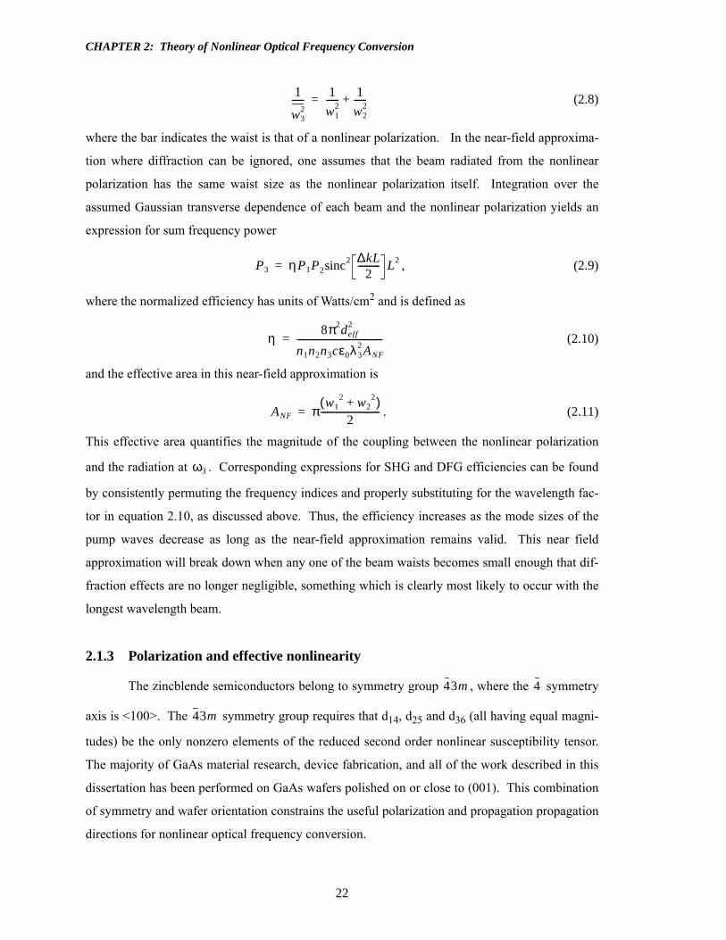
CHAPTER 2: Theory of Nonlinear Optical Frequency Conversion
22
(2.8)
where the bar indicates the waist is that of a nonlinear polarization. In the near-field approxima-
tion where diffraction can be ignored, one assumes that the beam radiated from the nonlinear
polarization has the same waist size as the nonlinear polarization itself. Integration over the
assumed Gaussian transverse dependence of each beam and the nonlinear polarization yields an
expression for sum frequency power
, (2.9)
where the normalized efficiency has units of Watts/cm2 and is defined as
(2.10)
and the effective area in this near-field approximation is
. (2.11)
This effective area quantifies the magnitude of the coupling between the nonlinear polarization
and the radiation at . Corresponding expressions for SHG and DFG efficiencies can be found
by consistently permuting the frequency indices and properly substituting for the wavelength fac-
tor in equation 2.10, as discussed above. Thus, the efficiency increases as the mode sizes of the
pump waves decrease as long as the near-field approximation remains valid. This near field
approximation will break down when any one of the beam waists becomes small enough that dif-
fraction effects are no longer negligible, something which is clearly most likely to occur with the
longest wavelength beam.
2.1.3 Polarization and effective nonlinearity
The zincblende semiconductors belong to symmetry group , where the symmetry
axis is <100>. The symmetry group requires that d14, d25 and d36 (all having equal magni-
tudes) be the only nonzero elements of the reduced second order nonlinear susceptibility tensor.
The majority of GaAs material research, device fabrication, and all of the work described in this
dissertation has been performed on GaAs wafers polished on or close to (001). This combination
of symmetry and wafer orientation constrains the useful polarization and propagation propagation
directions for nonlinear optical frequency conversion.
1
w32
------ 1
w12
------ 1
w22
------+=
P3 ηP1P2sinc2 ∆kL2
---------- L2=
η8π2deff
2
n1n2n3cε0λ32 ANF
---------------------------------------=
ANF πw1
2 w22+( )
2---------------------------=
ω3
43m 4
43m

23
CHAPTER 2: Theory of Nonlinear Optical Frequency Conversion
The use of (001) wafers for our orientation-patterned growth requires that the optical k-
vectors must lie in or approximately (modulo the wafer misorientation) in (001) in order to achieve
long propagation lengths and high efficiencies, both for bulk and waveguide geometries. The
three nonlinear polarization components for frequency mixing in this crystal symmetry are
(2.12a)
(2.12b)
. (2.12c)
where and the notation here indicates the Fourier amplitude of the electric
field at frequency polarized along the x direction. It is clear immediately that the combination
of input and output wave polarizations must have some projection along all of the x, y and z axes
in order for the effective nonlinearity to be nonzero. To explore the effects of propagation direc-
tion and polarization on the effective nonlinearity, we define a set of angles according to the dia-
gram in Figure 2.1. Here is defined as the angle in the (001) plane between the k-vector and the
y-axis [010], so that the electric field vector lies in the x-z plane when . and are
defined as the angles between the (001) plane and the electric field vector at frequency and
, respectively, as illustrated in Figure 2.1. Thus, when , the electric field vector lies
along the x-axis. Using these variables we can write the nonlinear polarizations as
(2.13)
(2.14)
Figure 2.1: Reference angles used for calculation of GaAs effective nonlinearsusceptibilities.
Px2( ) ω3( ) 2ε0d14 Ey ω1( )Ez ω2( ) Ez ω1( )Ey ω2( )+[ ]=
Py2( ) ω3( ) 2ε0d14 Ex ω1( )Ez ω2( ) Ez ω1( )Ey ω2( )+[ ]=
Pz2( ) ω3( ) 2ε0d14 Ex ω1( )Ey ω2( ) Ey ω1( )Ex ω2( )+[ ]=
ω3 ω2 ω1±= Ex ω1( )
ω1
φ
z[001 ]
φ
θ
E
wafer plane(001)
[010 ]
[100 ]
k
y
xφ
φ 0= θ1 θ2
ω1
ω2 θ φ 0= =
Px2( ) ω3( ) 2ε0d14 φsin x θ1 θ2 θ2 θ1sincos+sincos[ ] Eω1
Eω2=
Py2( ) ω3( ) 2ε0d14 φcos y θ1 θ2 θ2 θ1sincos+sincos[ ] Eω1
Eω2=
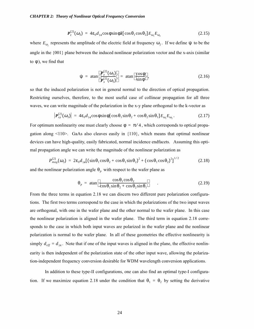
CHAPTER 2: Theory of Nonlinear Optical Frequency Conversion
24
(2.15)
where represents the amplitude of the electric field at frequency . If we define to be the
angle in the {001} plane between the induced nonlinear polarization vector and the x-axis (similar
to ), we find that
, (2.16)
so that the induced polarization is not in general normal to the direction of optical propagation.
Restricting ourselves, therefore, to the most useful case of collinear propagation for all three
waves, we can write magnitude of the polarization in the x-y plane orthogonal to the k-vector as
. (2.17)
For optimum nonlinearity one must clearly choose , which corresponds to optical propa-
gation along <110>. GaAs also cleaves easily in {110}, which means that optimal nonlinear
devices can have high-quality, easily fabricated, normal incidence endfacets. Assuming this opti-
mal propagation angle we can write the magnitude of the nonlinear polarization as
(2.18)
and the nonlinear polarization angle with respect to the wafer plane as
. (2.19)
From the three terms in equation 2.18 we can discern two different pure polarization configura-
tions. The first two terms correspond to the case in which the polarizations of the two input waves
are orthogonal, with one in the wafer plane and the other normal to the wafer plane. In this case
the nonlinear polarization is aligned in the wafer plane. The third term in equation 2.18 corre-
sponds to the case in which both input waves are polarized in the wafer plane and the nonlinear
polarization is normal to the wafer plane. In all of these geometries the effective nonlinearity is
simply . Note that if one of the input waves is aligned in the plane, the effective nonlin-
earity is then independent of the polarization state of the other input wave, allowing the polariza-
tion-independent frequency conversion desirable for WDM wavelength conversion applications.
In addition to these type-II configurations, one can also find an optimal type-I configura-
tion. If we maximize equation 2.18 under the condition that by setting the derivative
Pz2( ) ω3( ) 4ε0d14 φ φz θ1 θ2coscos[ ] Eω1
Eω2sincos=
Eωjωj ψ
φ
ψPy
2( ) ω3( )Px
2( ) ω3( )--------------------
atanφcosφsin
------------ atan= =
Pxy2( ) ω3( ) 4ε0d14 φcos φ θ1 θ2 θ2 θ1sincos+sincos[ ] Eω1
Eω2sin=
φ π 4⁄=
Pmag2( ) ω3( ) 2ε0d14 θ1sin θ2 θ1 θ2sincos+cos( )2 θ1 θ2coscos( )2+[ ] 1 2⁄
=
θp
θp
θ1 θ2coscosθ1 θ2 θ2 θ1sincos+sincos
-------------------------------------------------------------- atan=
deff d= 14
θ1 θ2=

25
CHAPTER 2: Theory of Nonlinear Optical Frequency Conversion
with respect to equal to zero, we find that θ3 = θ1 = θ2 = 35.26°, which corresponds to align-
ment of all polarizations along <111>. The effective nonlinearity obtained in this case is
, (2.20)
which is the maximum obtainable from a material with this symmetry.
2.1.4 Quasiphasematching
As some dispersion of the refractive indices is present in all materials, in general
and high conversion efficiencies are achieveable only by employing some phasematching tech-
nique. In birefringent crystals, propagation directions and polarization states can be selected so
that the wave-vector mismatch vanishes, but this is only true for a limited number of materials and
even then often over only limited wavelength ranges. Quasiphasematching provides a more flexi-
ble techique for obtaining phasematching provided some technique can be found for fabricating
the materials. In a quasiphasematched interaction, the magnitude and/or sign of effective nonlin-
earity is modulated periodically along the propagation direction of the radiation and can be
expressed as a Fourier series
(2.21)
where the grating vector is defined as and the is the period of the modulation.
If the sign of the susceptibility is modulated, the amplitude of the mth Fourier coefficient is
(2.22)
where is the duty cycle (0 < D < 1) of the reversed domains. The maximum nonlinearity is
obtained with lowest-order quasiphasematching (m = 1), and equal length domains ( )
. (2.23)
Inserting this definition of the nonlinearity from equation 2.23 into equation 2.4c and following
through the same derivation as Section 2.12 gives
(2.24)
where . Addition of the proper nonlinear susceptibility modulation thus makes
possible compensation of the dispersion and wave vector mismatch for any desired frequency con-
θ
deff2
3-------d14=
∆k 0≠
d z( ) deff Gm iKmz–( )expm ∞–=
m ∞=
∑=
Km 2πm Λ⁄= Λ
Gm2
mπ------- mπD( )sin=
D
D 1 2⁄=
dQPM2π---deff=
P3 ηQPMP1P2L2sinc2 ∆k Km–( )L
2----------------------------=
ηQPM η 2 π⁄( )2=

CHAPTER 2: Theory of Nonlinear Optical Frequency Conversion
26
version process by simple adjustment of the modulation period. Where previously the wave vector
mismatch limited the effective interaction length to the 4 µm - 100 µm range, with the quasiphase-
matching grating the device length can be arbitrarily long. Devices having interaction lengths >
5 cm have been demonstrated in PPLN and other materials. The reduction in the prefactor by
for this quasiphasematched interaction is a small price to pay for the many orders of mag-
nitude increase in effective length and the much higher efficiency it enables.
2.1.5 Attenuation effects
The presence of attenuation at one or more wavelengths will reduce the conversion effi-
ciencies and modify the tuning behavior of a nonlinear optical device. The functional similarity of
the coupled equations for the planar wavefront case and the waveguide case will allow us to derive
a single correction factor for the conversion efficiency in the presence of loss that applies to both
cases. With power losses of , , and at wavelengths , , and , respectively, the cou-
pled equations 2.4 are transformed into the form
. (2.25)
Solution of this equation yields a significantly more complicated expression for the efficiency and
tuning behavior. Comparing the lossy device with a lossless device, we can define an efficiency
reduction factor . Examining only the phasematched case and defining
, one finds this efficiency reduction factor to be
. (2.26)
For devices with losses at only , or some combination , the output power saturates with
length as the numerator is approximately 1 and the factor in the denominator cancels the para-
bolic gain in the lossless expression. With losses at all wavelengths, the converted power will
exhibit a maximum at a particular crystal length and then decrease for longer crystals. Attenuta-
tion losses thus limit the useable crystal lengths and therefore the obtainable efficiencies from a
particular material or device. The effects on tuning behavior can be calculated from the solution of
equation 2.25 and will affect the tuning behavior primarily around . Note that for
the special condition of , the efficiency is simply multipled by the attenuation factor
, as can be seen by expanding the quantity in square brackets as a Taylor series.
2 π⁄( )2
α1 α2 α3 λ1 λ2 λ3
zddE3 α3
2-----E3+ i
ω3deff
n3c--------------E2E1 i ∆k Km–( )z
α1 α2+( )2
-----------------------– zexp=
γ Plossy Plossless⁄=
α' α1 α2 α3–+=
γα– 3L( ) α'– L( ) 1–exp[ ]exp 2
α'2L2-------------------------------------------------------------------=
α3 α1 α2+
L2
x x⁄sin 0→
α' 0=
α– 3L( )exp
27
CHAPTER 2: Theory of Nonlinear Optical Frequency Conversion
2.2 Frequency conversion in waveguides
This section will develop the expressions necessary to predict the efficiency of frequency
conversion in semiconductor waveguides, then examine some interesting device examples.
Waveguide modes and nonlinear optics in waveguides have been investigated extensively, so I will
present only the parts of the derivation necessary to be internally consistent and to outline the
approximations employed, directing those interested to more detailed treatments [3-5]. The chap-
ter starts with a brief overview of waveguide mode properties, then develops effective areas which
properly account for the transverse mode overlap of the nonlinear polarization and radiated mode.
Nondimensional solutions for 1-dimensional planar waveguides with four layers are developed
and these are used to find nondimensional overlap integrals, which are used in turn to caluculate
the efficiencies of waveguide NLO devices.
2.2.1 Mode normalization
The stable modes of a dielectric waveguide structure propagate like plane waves, but their
transverse beam properties are set by the boundary conditions on the electric and magnetic fields
rather than by simple diffraction. Such a waveguide has a discrete spectrum of modes which are
orthonormal and which have differing transverse electric and magnetic field dependences. While
a waveguide may support many modes at a particular wavelength, for nonlinear optical frequency
conversion one is almost always interested in conversion to and from a single transverse mode at
each wavelength, both because this yields the highest efficiencies and because modal dispersion
usually insures that only one combination will be phasematched at a time. Additionally, since we
are considering collinear frequency conversion, we include only the forward propagating waves,
though the formalism can easily be extended to include non-collinear interactions such as the
backward OPO.
One can write the electric and magnetic fields of a guided mode propagating without
change in amplitude as
(2.27a)
(2.27b)
where and the modal index is . These modes exhibit the following orthonormal-
ization relationship,
, (2.28)
Eν x y z, ,( ) Eν x y,( ) i– βz( )exp=
Hν x y z, ,( ) Hν x y,( ) iβz–( )exp=
β 2πnν λ⁄= nν
12--- Re Eν x y,( ) Hµ
∗ x y,( )×[ ] z⋅ xd yd∫∞–
∞
∫ δνµPν=

CHAPTER 2: Theory of Nonlinear Optical Frequency Conversion
28
where is the power carried by the mode. For many waveguides used in nonlinear optics, one
can make the “weak-guidance” approximation, in which the z-components of the fields are
neglected and one considers only the transverse components. In this approximation the electric
and magnetic components of a particular mode are proportional and related by
. (2.29)
This approximation allows the definition of a simpler scalar normalization which depends only on
the modal electric field and which is extremely convenient for nonlinear optical calculations
. (2.30)
The modal electric field can then be written as the product of a complex amplitude, a -indepen-
dent normalized transverse field profile, and a rapidly varying phase factor
, (2.31)
so that the power carried by the mode is
. (2.32)
This mode normalization will be assumed for all subsequent waveguide calculations in this disser-
tation. In the next section, the factor will be allowed to vary with to derive a set of coupled
equations for the mode amplitudes.
Accurate solutions of 2-dimensional mode profiles typically requires numerical evaluation
of the modal propagation constants and field profiles. A variety of methods are used to find the
eigenvectors and values, including finite difference [6, 7] (and references therein), finite element
[8], and beam propagation techniques [3]. For semiconductor waveguides, these methods require
taking account of the exact structure formed by the particular lateral confinement technique used,
whether an etched rib, or a regrown buried heterostructure. We used a 2-D finite difference algo-
rithm to compute mode indices and transverse profiles for our devices; the specific implementa-
tion will be discussed in Chapter 4 along with the device design issues.
For some waveguides one can approximate the modes as being separable, so that
(2.33)
and the normalization becomes
Pν
Hν x y,( )ε0
µ0-----nν z Eν x y,( )×≈
Eν˜ x y,( )Eµ
˜ x y,( )∞–
∞
∫ dxdy δνµ=
z
Eν x y z, ,( ) AνEν x y,( ) iβz( )exp=
Pνnνε0c
2------------- Av
2=
Aν z
Eν˜ x y,( ) Evx
˜ x( )Eνy˜ y( )≈
29
CHAPTER 2: Theory of Nonlinear Optical Frequency Conversion
. (2.34)
This approximation, of which the effective index method [9, 10] is an example, provides a simpler
though less accurate technique for estimating the transverse modal profiles, since the two-dimen-
sional problem reduces to two separate one-dimensional problems.
2.2.2 Efficiency and effective area
If one allows the modes at each frequency to have a slowly varying envelope in the
direction in a manner similar to that used for plane waves in Section 2.1.1
, (2.35)
one can write a set of coupled equations for the s which have the same functional form as
those developed for plane waves. The efficiency of a waveguide sum frequency generation device
can therefore be written as
(2.36)
and the normalized efficiency has the same factors as in the previous section
. (2.37)
To move from sum frequency generation to harmonic generation and difference frequency genera-
tion one must simply replace with either or as discussed above in Section 2.1.2 to
obtain the proper normalized efficiency. The different factor still has units of area and is
defined as
. (2.38)
This effective area quantifies the physical size of the waveguide and magnitude of the coupling
between the nonlinear polarization and the waveguide mode at the generated frequency, being
equivalent to the area of the top-hat modes which would have the same conversion efficiency.
Thus, the calculation of efficiencies for collinear guided-wave nonlinear interactions reduces to
the calculation of the relevant overlap integrals, which will be investigated in more detail for spe-
cialized cases in the following section. Under the assumption that the waveguide modes are sepa-
Eνx x( )Eµx x( ) xd
∞–
∞
∫ Eνy y( )Eµy y( ) yd
∞–
∞
∫ δνµ= =
Aν z( )
z
Eν x y z, ,( ) Eν x y,( )Aν z( ) i– βz( )exp=
A j z( )
P3 ηwgP1 0( )P2 0( )L2sinc2 ∆β Km–( )L2
-----------------------------=
ηwg
ηwg
8π2deff2
n1n2n3cε0λ32 Aeff
---------------------------------------=
λ3 λ f λDFG
Aeff
Aeff ϑ 2– E1 x y,( )E2 x y,( )E3 x y,( ) xd yd∫∞–
∞
∫2–
= =

CHAPTER 2: Theory of Nonlinear Optical Frequency Conversion
30
rable, one can write the overlap integral as the product of separate 1-dimensional overlap integrals
in each transverse dimension , where
(2.39)
. (2.40)
2.2.3 One-dimensional slab waveguides
In this section we find the normalized modes of a 4-layer planar waveguide structure,
since this strucuture is typical of those fabricable in semiconductor materials. We follow the
approach of Kogelnik and Ramaswamy [11] using normalized mode parameters, but extend this to
a four layer structure with a top cladding between the waveguide core and air. Determination of
these four-layer mode solutions makes possible computation of the normalized overlap integrals in
the following section, which in turn allows easy estimation of the potential efficiencies obtainable
for various interesting NLO waveguide devices. Only the TE modes of the structure are investi-
gated here. The TM mode solutions can also be found, but use of the weak guidance approxima-
tion in calculating overlap integrals eliminates the distinction between the transverse dependence
of the TE and TM modes.
The four layer planar dielectric structure to be analyzed is shown in Figure 2.2. We con-
strain the index and composition of the top cladding layer to be same as the lower cladding under-
neath the core. This constraint allows exploration into the impact of the top cladding layer while
adding only one additional parameter. Additionally, this is a particularly suitable structure for
growth by molecular beam epitaxy, since the few effusion sources (typically two Ga and one Al
sources) can only be modulated on/off and therefore only a limited number of compositions can be
grown without ramping the source temperatures during a growth run.
In accordance with the normalized approach, we define normalized coordinates to make
the conclusions independent of the dimension and wavelength of the devices. Taking the core
width as the characteristic dimension of the waveguide in the x direction, one can define
. (2.41)
The one-dimensional transverse field profiles are then normalized according to
ϑ ϑ xϑ y=
ϑ x E1x x( )E2x x( )E3x x( ) x d
∞–
∞
∫=
ϑ y E1y y( )E2y y( )E3y y( ) y d
∞–
∞
∫=
ρ
X x ρ⁄=
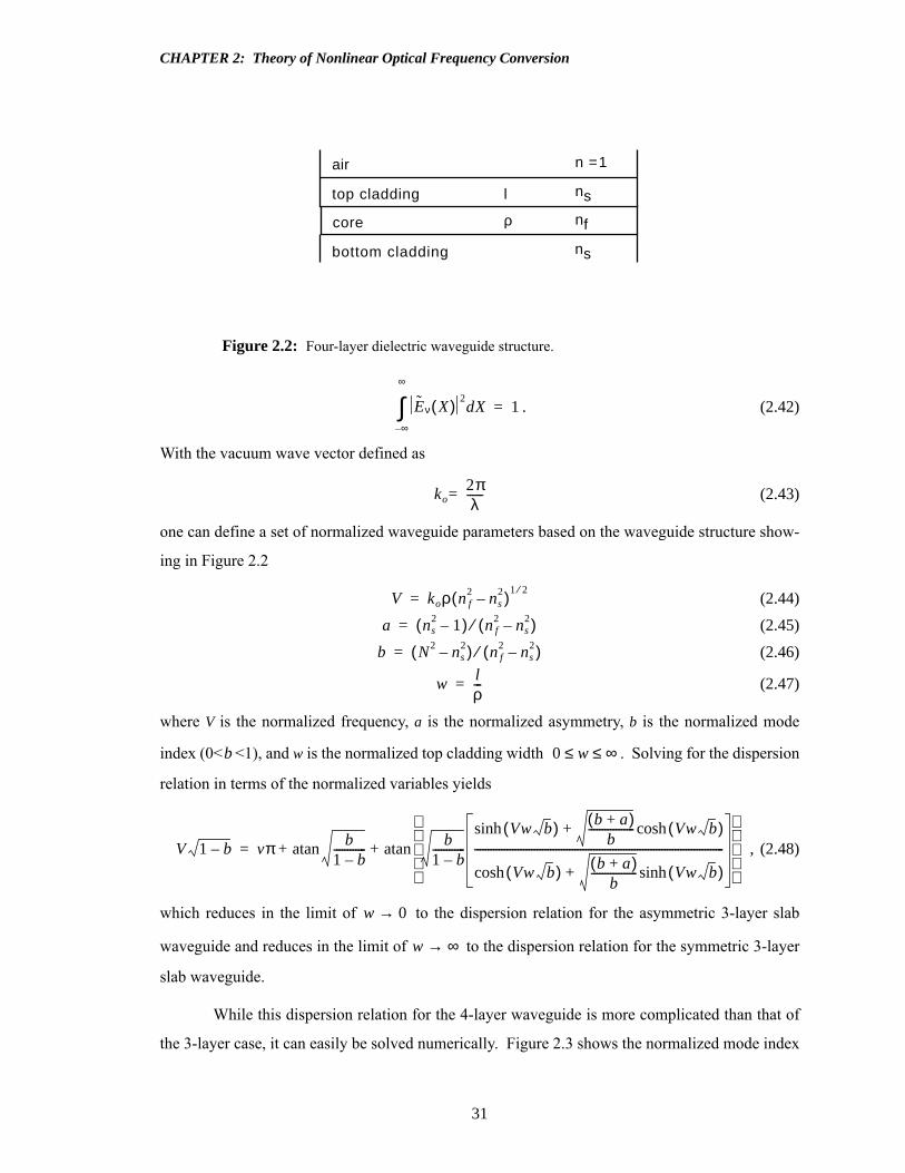
31
CHAPTER 2: Theory of Nonlinear Optical Frequency Conversion
. (2.42)
With the vacuum wave vector defined as
(2.43)
one can define a set of normalized waveguide parameters based on the waveguide structure show-
ing in Figure 2.2
(2.44)
(2.45)
(2.46)
(2.47)
where V is the normalized frequency, a is the normalized asymmetry, b is the normalized mode
index (0< <1), and w is the normalized top cladding width . Solving for the dispersion
relation in terms of the normalized variables yields
, (2.48)
which reduces in the limit of to the dispersion relation for the asymmetric 3-layer slab
waveguide and reduces in the limit of to the dispersion relation for the symmetric 3-layer
slab waveguide.
While this dispersion relation for the 4-layer waveguide is more complicated than that of
the 3-layer case, it can easily be solved numerically. Figure 2.3 shows the normalized mode index
Figure 2.2: Four-layer dielectric waveguide structure.
core
top cladding
air
bottom cladding
ρ
l
ns
nf
ns
n =1
Eν X( ) 2
∞–
∞
∫ dX 1=
ko2πλ
------=
V koρ n f2 ns
2–( )1 2⁄=
a ns2 1–( ) n f
2 ns2–( )⁄=
b N2 ns2–( ) n f
2 ns2–( )⁄=
wlρ---=
b 0 w ∞≤ ≤
V 1 b– vπ b1 b–------------ b
1 b–------------
Vw b( )sinh b a+( )b
----------------- Vw b( )cosh+
Vw b( )cosh b a+( )b
----------------- Vw b( )sinh+
--------------------------------------------------------------------------------------------
atan+atan+=
w 0→
w ∞→

CHAPTER 2: Theory of Nonlinear Optical Frequency Conversion
32
as a function of normalized confinement for various asymmetry and top cladding combinations.
The dashed curves show the classic solutions for various asymmetries without any top cladding
included in [11], while the solid curves show a waveguide with infinite asymmetry, but including
top cladding layers of varying normalized widths. Typical asymmetries for waveguides in
AlGaAs range between 5 and 40. Addition of a top cladding layer of equal thickness to the core
results in a mode index approximately equal to that of a symmetric waveguide for normalized con-
finements greater than . One can see that even relatively thin top cladding layers signifi-
cantly decrease the asymmetry and raise the mode index.
2.2.4 Mode overlaps of four-layer planar waveguides
This section presents one-dimensional overlap integrals for the normalized 4-layer
waveguides of the last section which can be used for the calculation of the conversion efficiencies,
as developed in Section 2.2.2. In general, this normalized overlap is a function of the waveguide
Figure 2.3: Normalized ω−β diagrams for three and four layer planar waveguides.The dashed curves are those of [12] for three-layers waveguides plotted for the twolowest order modes with asymmetries of 0, 1, 10 and ∞. The solid lines are for four-layer waveguides of infinite asymmetry but having normalized top claddingthicknesses of 0.1, 0.3, and 1.
0
0.2
0.4
0.6
0.8
1
0 1 2 3 4 5 6
b
V
a=0
w= 1
w = 0.3
∞a=
w = 0.1
a=0 a=0 ∞a=
w = 1
w= 0.3
w = 0.1
1
1 10
V 2=
33
CHAPTER 2: Theory of Nonlinear Optical Frequency Conversion
parameters, the three wavelengths of interest, as well as the dispersion of the materials between
those wavelengths. We expand the analysis of Lim, et al[5, 13], who investigated symmetric and
asymmetric 3-layer structures for harmonic generation, by extending here the analysis to 4-layers
and arbitrary frequency interactions. Following Lim, et al [5, 13] we can define a dispersion
parameter between and as
(2.49)
and a non-degeneracy parameter δ which relates the various wavelengths , , and accord-
ing to
and (2.50)
where . Using these we can then express the normalized confinement at the three wave-
lengths as
and (2.51)
which can be inverted to yield
and (2.52)
With these definitions and the previous definitions of we can define a normalized depth in one
dimension as
(2.53)
so that the Thus, if the transverse mode is assumed to be separable, the effec-
tive area can be expressed in terms of the characteristic dimensions as
. (2.54)
provides a dimensionless parameter which quantifies the overlap of the three modes in the
interaction independent of the wavelengths or waveguide dimensions. The expression is written as
a function of the normalized confinement at the longest wavelength, , because this mode is
closest to cut-off and therefore has the most implications for device design.
rij λ i λ j
rij
n f2 ns
2–( )i
n f2 ns
2–( ) j
-----------------------=
λ1 λ2 λ3
λ1
λ3----- 2
1 δ–-----------=
λ2
λ3----- 2
1 δ+------------=
δ 1<
V1 V31 δ–
2-----------
r13= V2 V31 δ+
2------------
r23=
V21 δ+1 δ–------------
r23
r13------V1= V3
2
1 δ–( ) r13
---------------------------V1=
E j
Dx E1˜ V1 w a δ X, , , ,( )E2
˜ V1 w a δ r23 r13 X, , , , , ,( )E3˜ V1 w a δ r13 X, , , , ,( ) X ˙d
∞–
∞
∫2–
=
1 D jρ j( )⁄ ϑ j2=
Aeff ρxDxρyDy=
D
V1

CHAPTER 2: Theory of Nonlinear Optical Frequency Conversion
34
More useful for device design is the nondimensional depth parameter , because it is
proportional to the effective depth for a given core-cladding index difference. Since con-
version efficiencies are proportional to the inverse of effective depth, it makes sense to plot the
reciprocal which is proportional to conversion efficiency and has a maximum at the point
of minimum effective depth. Figure 2.4 shows as a function of for the values
, , and . For the semiconductor materials under consideration, the
overlaps are relatively weak functions of the dispersion parameters, so we plot the cases where
. The parameter exhibits a maximum value corresponding to the opti-
mum 1-D overlap which is relatively constant as a function of top cladding thickness for this
degenerate case, though the value of corresponding to this maximum varies over the transition
from asymmetric to symmetric waveguides. The relative insensitivity of this maximum will allow
optimization of the waveguide structures for other important factors such as noncriticality or low
scattering losses without large sacrifices in conversion efficiency.
Defining and to be values of and associated with this maximum achieve-
able confinement, we can explore the behavior of , the optimal normalized depth
parameter, as a function of the normalized device parameters. Figure 2.5 shows as a
Figure 2.4: Nondimensional depth parameter as a function of normalized frequencyand cladding width.
DV1( )
Dρ( )
DV1( ) 1–
DV1( ) 1– V1
w 0 1 ∞, ,= a ∞= δ 0=
r13 r23 1= = DV1( ) 1–
V1
0
0.05
0.1
0.15
0.2
0.25
0.3
0.35
0.4
0 0.5 1 1.5 2 2.5 3 3.5 4
(DV
)-1
V1
w=0w=1w=inf
Dopt Vopt D V1
DoptVopt( ) 1–
DoptVopt( ) 1–

35
CHAPTER 2: Theory of Nonlinear Optical Frequency Conversion
function of the normalized top cladding thickness for values of the degeneracy parameter
.
The figure is plotted for a typical asymmetry of 20 corresponding to and
thus an approximately 30% difference in Al fraction for AlGaAs. The magnitude is a
strong function of the top cladding width only far from degeneracy and at low cladding widths,
where the addition of a thin top cladding makes possible better overlap between the modes at dif-
ferent wavelengths. The highest efficiencies are obtained for normalized top cladding thicknesses
of around , though even in the case the increase resulting from addition of the
cladding is only about 20%. One can also see from the graph that the dependence of efficiency on
the degeneracy parameter is roughly independent of top cladding thickness for normalized clad-
ding thicknesses greater than 0.5. Also, though this is not shown in Figure 2.5, the curves are only
weakly dependent on the assumed asymmetry except near ; intuitively, most of the varia-
tion with asymmetry occurs when the top cladding layers are very thin, since otherwise the top
cladding layer determines the mode profiles.
2.2.5 Waveguide NLO device predictions
We can use the predictions of the last section to estimate conversion efficiencies for useful
nonlinear optical devices such as difference frequency generators for IR generation. For simplic-
Figure 2.5: Optimal depth parameter as a function of the normalized top claddingwidth and nondegeneracy.
w
δ 0 0.3 0.6 0.9, , ,=
0.26
0.28
0.3
0.32
0.34
0.36
0.38
0.4
0.42
0 0.5 1 1.5 2 2.5 3
(Do
ptV
op
t)-1
w
δ = 0
δ = 0.3
δ = 0.6
δ = 0.9
∆ncore cladding– 0.15=
DoptVopt( ) 1–
w 0.5≈ δ 0.9=
w 0=

CHAPTER 2: Theory of Nonlinear Optical Frequency Conversion
36
ity, we consider a completely symmetric hetrostructure waveguide in which the core region is sur-
rounded entirely by a uniform refractive index cladding, as shown in Figure 2.6.
We make the simplifying assumptions that the mode profile is separable in the transverse dimen-
sions and that we can approximate the 2-D overlap by a product of 1-D overlaps, as discussed in
the previous sections. The approach of Marcatili [14] approximates the two-dimensional mode of
such a buried rectangular waveguide as a product of two one-dimensional waveguide modes, the
first satisfying TE boundary conditions in one direction and the other satisfying TM boundary con-
ditions in the orthogonal direction. In the weak guidance approximation, these TE and TM modal
profiles are identical, so the waveguide mode can be approximated simply by the product of two
one-dimensional modes of the kind developed in section 1.2.3. This allows straightforward use of
the normalized formalism and results of the previous section. Assuming the top cladding is suffi-
ciently thick, we can treat the vertical mode as symmetric and use those values for
for both the vertical and horizontal modes.
With these approximations, the efficiency for difference frequency generation can be
found from equations 2.54, 2.44 and 2.37 to be
(2.55)
for = 57 pm/V and a refractive index of 3.2. The generated wavelength is the longest
wavelength and the approximation
(2.56)
is assumed valid. From Figure 2.5 one can determine the values of and find an esti-
mated efficiency. The efficiency exhibits an extremely strong wavelength dependence and is lin-
Figure 2.6: Schematic diagram of the buried heterostructure used for waveguidedevice calculations.
corenf
top claddingns
lower claddingns
DoptVopt( ) 1–
ηwg1
W cm2⋅-------------------
64π4deff2 ∆n
n2cε0λ14 DoptVopt( )2
---------------------------------------------- 7.447 4×10 ∆n( )λ1
4 µm[ ] DoptVopt( )2----------------------------------------------= =
deff λ1
n f2 ns
2– 2ns∆n≈
DoptVopt( ) 1–

37
CHAPTER 2: Theory of Nonlinear Optical Frequency Conversion
ear in the core-cladding refractive index difference. To make the results independent of
wavelength, Figure 2.7 plots the product as a function of and . The efficiency varies
by approximately a factor of 2 between the degenerate and highly nondegenerate cases. With
pumps in the near-IR, DFG of 10 µm radiation could achieve efficiencies of 0.1 (W*cm2)-1 with
= 0.1, which corresponds to a composition difference of approximately 20% Al in AlGaAs.
This efficiency would allow generation of 1 mW of 10 µm radiation in a 1 cm long orientation-pat-
terned GaAs waveguide with only 100 mW of pump radiation at each of the pump wavelengths.
The same 100 mW could generate 10 µW of output at 10 µm wavelength in only a 1 mm long ori-
entation patterned AlGaAs waveguide, a power level which is still very useful for spectroscopic
applications. This means that even relatively high loss AlGaAs waveguide devices such as those
characterized in chapter 4 may be useful for mid-IR generation, with their utility increasing as the
losses improve with further research. Of course, methods for coupling the pump beams into such
highly multi-moded waveguides will need to be developed to achieve these efficiencies, some-
thing discussed in more detail in Chapter 4.
Optical parametric oscillators could also be developed in these waveguides, but the high
propagation losses measured to date at near-IR pump wavelengths have been too large to consider
this as a realistic possibility. However, future advances in lowering attenuation losses could make
this an attractive option for achieving high conversion efficiencies.
Figure 2.7: DFG efficiency for AlGaAs waveguides as a function of core-claddingconfinement.
ηwgλ14 ∆n δ
∆n
0
1000
2000
3000
4000
5000
0 0.1 0.2 0.3 0.4
ηλ4
(µm
4/W
*cm
2)
∆ n
δ = 0
0.3
0.6
0.9

CHAPTER 2: Theory of Nonlinear Optical Frequency Conversion
38
2.3 Bulk single-pass NLO CW devices
In this section we extend the expressions derived for plane wave frequency conversion to
realistic devices and predict GaAs device performance for low power applications. The section
begins with calculation of the performance of difference frequency generation devices, then
briefly outlines harmonic generation for comparison with our experimental results in Chapter 5.
Discussion of OPOs and other high power devices will be delayed until Chapter 6, which will
investigate the limitations on high-peak-power and high-average-power devices.
2.3.1 Difference frequency generation
To estimate the conversion efficiencies obtainable in GaAs for mid-IR generation, we can
use equations 2.8, 2.9, and 2.10 and make some reasonable assumptions regarding the beam sizes.
If we assume that the generated DFG wavelength is much larger than either of the pump wave-
lengths, diffraction will affect the long wavelength beam under conditions for which the other two
beams remain within their near field limits. As the pump beams are focused more and more
tightly, the radiated idler beam will begin to diffract away rapidly from the driving idler polariza-
tion region and the efficiency and beam quality will be compromised. We can estimate the con-
version efficiency of a DFG device producing a good quality idler beam by setting the generated
idler polarization to be confocal in the crystal, so that the effect of diffraction on the conversion
efficiency will not be too large. This condition is the lower limit on the use of the near-field
approximation.
If the electric field of the gaussian pump beams have the transverse dependence
, (2.57)
where the beam waist transforms according to
(2.58)
the idler polarization will have a similar gaussian transverse profile with a local waist of
, (2.59)
though this idler polarization will obviously not transform longitudinally as a Gaussian beam.
This case is in constrast to harmonic generation, where the product of two identical gaussian
beams produces a harmonic polarization that also propagates as a gaussian beam. In the confocal
Er2
w z( )2-------------–
exp∝
w z( ) w0 1zzR
----- 2
+=
1
wi2 z( )
------------- 1
wp2 z( )
------------- 1
ws2 z( )
-------------+=
39
CHAPTER 2: Theory of Nonlinear Optical Frequency Conversion
approximation we ignore the z dependence of all beams and choose the pump focusing to make the
waist of the idler polarization the same as that of a confocally focused beam of the idler wave-
length in the crystal, so that
(2.60)
The pump and signal waists make symmetric contributions to the size of the idler beam, so we
assume them here to be equal. The optimal efficiency is actually obtained with the pump and sig-
nal having equal confocal parameters rather than equal waist sizes. However, in the highly non-
degenerate case, the two conditions are approximately the same. Using the expression for the
Rayleigh length, we obtain an expression for the DFG power at zero phase mismatch in the confo-
cal idler approximation
(2.61)
where
. (2.62)
Again, the refractive index is assumed to be 3.2 and to be 57 pm/V. The DFG efficiency for
generating 10 µm radiation is approximately (W*cm)-1. With 100 mW at each of the
pump wavelengths and a 1 cm long bulk OPGaAs crystal, the output power would be 1 µW, which
is a factor of 103 lower than that of the waveguide device having the same 1 cm length. However,
the high losses measured in waveguide devices at present make bulk and waveguide devices more
comparable, since useful waveguide lengths will be in the < mm regime. The bulk crystal avoids
the waveguide’s pump power limitations arising from the very small waveguide end-facet areas.
With the much lower attenuation losses measured in bulk OPGaAs compared to waveguide
devices, longer crystals can be used. 1 Watt of power at each pump wavelength and a 3-cm-long
OPGaAs crystal could achieve 1 mW DFG power at 10 µm using crystals comparable to those
already demonstrated.
Further investigation of the effects of focusing and diffraction on DFG efficiency [15, 16]
have been performed by Guha, and Mayet. The gain in efficiency with tighter focusing begins to
saturate around the confocal idler condition and exhibits a maximum in the vicinity of a confocal
pump condition, but that maximum is relatively broad, with similar efficiencies obtained across a
wide range of focusing conditions. More potentially complicating for many applications is the
L 2zR 2πwidler
2
λ idler
----------------= =
PDFG
P2------------ ηDFGP1L=
ηDFG1
W cm⋅-----------------
8π2deff2
n2cε0λDFG3
------------------------- 9.4 2–×10
λ13 µm[ ]
---------------------= =
deff
1 4–×10

CHAPTER 2: Theory of Nonlinear Optical Frequency Conversion
40
impact of focusing on the beam quality. Mayet investigated the M2 value of the DFG beam as a
function of focusing and found that the confocal idler case resulted in M2 values around 1, while
M2 > 1 for the confocal pump situation. When the pump is confocal, the M2 value is a function
of the non-degeneracy. At degeneracy the confocal pump case has an M2 value of 1.03, while for
the case the M2 at the same focusing condition is 1.32. Thus, depending on the applica-
tion, one can trade-off between maximum efficiency around the pump confocal condition and
higher beam quality available at the confocal idler condition. More detailed analysis of these
focusing effects is outside the scope of this dissertation, but will be required for optimization of the
devices.
2.3.2 Second harmonic generation
Second harmonic generation is useful for mid-IR generation though frequency doubling of
CO2 lasers. For our purposes it provides an easier tool for evaluating new materials, since only
one input beam is required. The effects of focusing on second harmonic generation efficiency have
been analyzed in detail by Boyd and Kleinman [17] and only the results will be presented here.
For a beam of wavelength focused into a crystal of length L and refractive index with a waist
of 1/e2 radius , one can define a normalized focusing parameter which
characterizes the focusing of the beam in a crystal. Boyd and Kleinman define a function
which includes the impact of focusing on the SHG efficiency. is a normalized walkoff length,
but since GaAs has an isotropic refractive index, for all nonlinear optical interactions at
normal incidence and there are no length limitations due to Poynting vector walkoff. For optimum
phase mismatch, which is not necessarily in the focused case, the maximum conversion
efficiency for a particular focusing condition is
, (2.63)
where is the k-vector for the fundamental beam in the crystal. The optimum efficiency is found
at , where the h factor is 1.2. For harmonic generation of 5 µm radiation using a
10 µm fundamental beam in a 1 cm long GaAs crystal, one obtains a conversion efficiency of
(W*cm)-1. The approximate factor of 2 difference between the efficiency for SHG with
δ 2 3⁄=
λ n
w0 ξ L2zR
-------- Lλ2πw0
2n----------------= =
h B ξ,( )
B
B 0=
∆k 0=
P2
P1-----
8πdeff2
n2n12cε0λ1
2------------------------P1k1Lh B ξ,( )=
k1
L 5.74zR=
2.1 4–×10

41
CHAPTER 2: Theory of Nonlinear Optical Frequency Conversion
a 10 µm fundamental and the efficiency for DFG generation of 10 µm arises from the different
waists used to calculate the effective area in equation 2.11. For SHG the 10 µm pump waves are
confocally focused in the crystal, while for DFG the pump waves in the near-IR have waists larger
by to generate a confocally focused idler wave.
2.4 Conclusion
In this chapter we developed expressions for the conversion efficiency of various low-
power nonlinear optical devices, in both plane-wave and confocal approximations, focusing pri-
marily on difference frequency generation. Additionally, we investigated the effects of top clad-
ding layers on the modes of 4-layer slab waveguides, calculated the effective areas of waveguide
devices as a function of the normalized waveguide parameters such as confinement and degener-
acy, and estimated the conversion efficiencies achieveable in waveguide devices.
2

CHAPTER 2: Theory of Nonlinear Optical Frequency Conversion
42
References
1. R.W. Boyd, Nonlinear Optics (Academic Press, San Diego, 1992).
2. Y.R. Shen, The Principles of Nonlinear Optics (John Wiley & Sons, New York, 1984).
3. D. Marcuse, Theory of Dielectric Waveguides, Quantum Electronics -- Principles and Appli-
cations, P.F. Luao and P.L. Kelley eds. (Academic Press, San Diego, 2nd ed., 1991).
4. A. Yariv, "Coupled-mode theory for guided-wave optics," IEEE J. Quantum Electron. QE-9,
919-933 (1973).
5. E.J. Lim, "Quasi-phasematching for guided-wave nonlinear optics in lithium niobate," Ph. D.
dissertation (Stanford University, Stanford, CA, 1992).
6. M.S. Stern, "Semivectorial polarised finite difference method for optical waveguides with
arbitrary index profiles," IEE Proc. J 135, 56-63 (1988).
7. M.S. Stern, "Rayleigh quotient solution of semivectorial field problems for optical
waveguides with arbitrary index profiles," IEE Proc. J 138, 185-190 (1991).
8. B.M.A. Rahman and J.B. Davies, "Vector-H finite element solution of GaAs/GaAlAs rib
waveguides," IEE Proc. J 132, 336-342 (1985).
9. G.B. Hocker and W.K. Burns, "Mode dispersion in diffused channel waveguides by the effec-
tive index method," Appl. Opt. 16, 113-118 (1977).
10. J. Buus, "The effective index method and its application to semiconductor lasers," IEEE J.
Quantum Electron. QE-18, 1083-1089 (1982).
11. H. Kogelnik, "Theory of dielectric waveguides," in Integrated Optics, T. Tamir ed. (Springer-
Verlag, New York, 1975) pp. 13-81.
12. H. Kogelnik and R.V. Ramaswamy, "Scaling rules for thin-film optical waveguides," Appl.
Opt. 13, 1857-1862 (1974).
13. E.J. Lim, S. Matsumoto, and M.M. Fejer, "Noncritical phase matching for guided-wave fre-
quency conversion," Appl. Phys. Lett. 57, 2294-2296 (1990).
14. E.A.J. Marcatili, "Dielectric rectangular waveguide and directional coupler for integrated
optics," Bell Syst. Tech. J. 48, 2071-2102 (1969).
15. S. Guha, F.J. Wu, and J. Falk, "The effects of focusing on parametric oscillation," IEEE J.
Quantum Electron. QE-18, 907-912 (1982).
16. J. Mayet, "Quasi-phase-matched frequency conversion of gaussian beams," report (Ginzton
Laboratory, Stanford University, Stanford, CA, 1996).
17. G.D. Boyd and D.A. Kleinman, "Parametric interaction of focused gaussian light beams," J.
Appl. Phys. 39, 3597-3639 (1968).

43
CHAPTER 3: All-Epitaxial Fabrication of GaAs Orientation Templates
Invention of an all-epitaxial orientation template fabrication process is the breakthrough
which made possible the growth of orientation-patterned films and therefore the optical device
results presented in subsequent chapters. This chapter surveys the background research relevant to
all-epitaxial template fabrication and describes in detail our investigations into template fabrica-
tion processes. We have successfully developed templates suitable for regrowth of orientation-
patterned bulk and waveguide devices. We have also explored improvements on this process
which could lead ultimately to higher performance nonlinear optical devices, particularly for
waveguide applications. Undoubtedly, this process can be refined much further than we have suc-
ceeded in doing to date and we hope that the combination of background, results, and suggestions
presented here will be useful for anyone pursuing similar investigations.
This chapter begins with an overview of the primary issues in template fabrication, after
which it reviews epitaxial growth of both Ge and GaAs on each other and also their integration to
form a GaAs/Ge/GaAs heterostructure. It then presents the results of our experiments in epitaxial
inversion, discusses them in the context of related research, and lays out profitable routes for
future exploration. The last sections address issues associated with template patterning, etch stop
behavior, and regrowth considerations.
3.1 Introduction
Epitaxial growth of orientation-patterned semiconductor films useful for quasi-phase-
matched nonlinear optics requires templates whose surface contains a modulation in crystalline
orientation with the proper period and duty cycle. There is little precedent for fabrication of such
controllably multi-orientation crystals and almost none for achieving it solely epitaxially. The
most successful patterned growth technique to date utilized wafer bonding to provide an inverted
layer and produced waveguide devices whose performance was limited by waveguide losses
attributed to longitudinal corrugation of the core-cladding boundaries [1]. The only previous all-
epitaxial attempt to solve this problem was made in II-VI materials [2]. Waveguides were fabri-
cated using this technique, but issues of corrugation associated with unequal epitaxial growth rates
for (001) and (111) surfaces resulted in very high waveguide losses.

CHAPTER 3: All-Epitaxial Fabrication of GaAs Orientation Templates
44
3.1.1 Overview
Since crystal quality considerations limit us to epitaxial growth techniques in materials
like GaAs, there are two possible strategies for achieving an all-epitaxial surface with two differ-
ent orientations present. Both utilize photolithography to set the domain periods and duty cycles,
making straightforward the fabrication of very short periods, the preservation of domain coherence
across the wafer, and the fabrication of different-period devices on the surface of a single wafer.
The first strategy starts with a wafer of a primary orientation and involves spatially selective
growth of secondary orientation material. This can be done using a self-patterning technique such
as ion-beam deposition or some kind of selective area epitaxy through a photolithographically
defined mask. The second possibility reverses the steps – the secondary crystal orientation is
grown uniformly in a thin layer across the primary orientation wafer surface. After deposition of a
photolithographically defined etch mask, one etches down through the thin film to expose the pri-
mary orientation resulting in the desired orientation template. Figure 3.1 illustrates both possibili-
ties. We have explored both of these approaches for template fabrication, but have focused
primarily on the etch-back approach for reasons of film quality which will become clearer as we
proceed.
Both of the above strategies will produce a corrugation in the template which may be pre-
served during subsequent regrowth. If this residual corrugation reaches the subsequently-grown
waveguiding layers, it will result in core-cladding interface corrugation and associated scattering
Figure 3.1: Two strategies for obtaining an all-epitaxial, orientation-patterned film.
+
-
+
- - -
+
-
+
+
- - -
orientation template
substrate +
lift-offetch-back
deposit/pattern masking layer
grow inverted GaAs layer
grow inverted GaAs layer
deposit/pattern masking layer
etch through GaAs/remove mask remove mask/GaAs

45
CHAPTER 3: All-Epitaxial Fabrication of GaAs Orientation Templates
losses in the waveguides. Therefore, we desire to minimize the template corrugation so as to
reduce the ultimate waveguide losses. Since the original template corrugation results primarily
from the total layer thickness required to achieve the epitaxial inversion, minimizing template
layer thicknesses is a high priority. It may be possible to planarize the film surface during subse-
quent regrowth, but reduction of the initial template corrugation will obviously make things easier.
One could also consider variations on the above strategies, such a slight back-etch through the
mask before growing the inverted layer in the lift-off approach so that a nominally flat template
surface results.
Regardless of how the orientation pattern is defined, some technique is required for modu-
lating the crystal growth in a fashion such that the nonlinear optical susceptibility seen by the opti-
cal radiation varies from section to section. In the absence of a spontaneous ferroelectric
polarization, this can only be achieved through a change in crystal orientation. As discussed in
chapter 2, the highest effective nonlinear susceptibility and the greatest efficiencies are achieved
when this modulation alternates sign, so that the two orientations differ by a crystallographic
inversion. The zincblende crystal structure consists of a face-centered crystal (fcc) lattice structure
with a two atom basis. Crystallographic inversion in a III-V zincblende semiconductor can be
understood simply as an exchange of the two basis atoms (Ga and As, for example) on their
respective sublattices, or equivalently as a reversal in direction of the single III-V bond which runs
along the <111> direction. Figure 3.2 illustrates the two phases.
Figure 3.2: GaAs unit cells showing both GaAs phases.
[ 001 ]
AsGa

CHAPTER 3: All-Epitaxial Fabrication of GaAs Orientation Templates
46
The relationship between the two energetically equivalent phases, which differ by the
desired crystal inversion, is designated "antiphase". Antiphase boundaries (APBs) separate
regions of opposite phase and can lie in several different atomic planes [3]. The APBs form planes
of incorrectly-bonded nearest neighbor atoms, As-As or Ga-Ga, with the exact configuration
depending on the plane in which the APD lies. Since zincblende crystals have symmetry group
, these phases differ by a 90° rotation about <001>, which is normal to the usual wafer sur-
face of (001). This inversion can be visualized by rotating one of the unit cells in Fig. 3.2 by 90°
about [001] and then lowering it by 1/4 of a unit cell to obtain the opposite phase. For (001)
wafers this symmetry relationship is highly desirable for subsequent regrowth of orientation-pat-
terned films because both phases have the same surface exposed, minimizing any asymmetry
between the growth rates and resulting corrugations. This eliminates the major corrugation-pro-
ducing complication in the work of Angell, et al. [2].
Obtaining an epitaxial inversion thus requires that all the column III and column V atoms
exchange sublattices at some point during crystal growth. If we imagine epitaxy as a simplistic
spraying of alternating layers of Ga and As, then one would need only to deposit two consecutive
layers (Ga, for example) of the same atomic species and then continue with the alternating
sequence to achieve crystal inversion, as shown in Figure 3.3. However, such a cation bilayer
would be extremely unstable and atomic exchange mechansims during subsequent deposition
would result in continued growth of material in phase with the substrate. In fact, relative stability
against such spontaneous antiphase twinning is clearly a necessary precondition for normal high-
quality epitaxial growth.
Figure 3.3: Gedanken epitaxial inversion with two consecutive atomic layers
43m
GaAs phase A
GaAs phase B
Ga bilayerGaAs

47
CHAPTER 3: All-Epitaxial Fabrication of GaAs Orientation Templates
Thinking more generally, any scheme which relies on an exact number of atomic mono-
layers separating the two GaAs phases is difficult to implement both for technological and funda-
mental reasons. Accurate calibration of growth rates to sub-monolayer precision is difficult to
accomplish. More importantly, rather than being a simple plane of atoms, the actual vacuum-
semiconductor interface exhibits a complicated free-energy-driven reconstruction with partially
complete atomic layers extending several monolayers into the crystal [4]. Not only does this fact
make the utility of depositing an exact number of monolayers unclear, but it also hints that the ulti-
mate orientation of the top GaAs will depend critically on the exact surface reconstruction.
A more realistic approach to epitaxial inversion uses a neutral buffer to isolate the two ori-
entations and governs nucleation of the secondary orientation by the buffer surface characteristics
rather than the thickness. A suitable buffer must meet several criteria. It must preserve crystal
quality so that subsequent layers are not highly defective. Precise buffer layer thickness should
not matter. There must be some method for nucleating the desired orientation on top of the buffer.
Finally, it is desirable that the buffer and secondary orientation layers of the template structure be
as thin as possible to minimize template corrugations which might propagate into device layers.
To find a neutral buffer layer, it is logical to look at those column IV semiconductors
which have been widely investigated for use in epitaxially-fabricated devices. These have the dia-
mond crystal structure, which is identical to the zincblende III-Vs except that both the atoms in the
basis are the same. Comparing the lattice constants of GaAs (5.6533 Å) with Si (5.4309 Å) and
Ge (5.6461 Å), we see that Si has a 4% lattice mismatch, while Ge has < 0.1 % mismatch. This
makes thick (> 1000Å) Ge layers possible without generation of misfit dislocations, whereas lat-
tice relaxation of Si layers grown on GaAs begins between 10 Å and 15 Å [5, 6]. These strain
effects on epitaxial inversion quality were confirmed by Koh, et al. who observed by cross-sec-
tional transmission electron microscopy that inverted films with Si buffer layers had much higher
densities of misfit dislocations than did those with Ge buffer layers [7, 8].
A more complicated problem is finding a technique for controlling the orientation of the
GaAs layer on top of Ge, since in general both GaAs domains (differing by a crystal inversion) can
nucleate and grow equally well on the higher symmetry Ge surface. GaAs growth on a neutral Ge
(100) surface produces a poly-domain GaAs film with a high density of antiphase domains
(APDs). Such highly defective films are not suitable for electrical or optical applications and a
great deal of research was devoted to polar-on-nonpolar epitaxy in the late 1980s and early 1990s
with the goal of hybrid integration of III-V and IV materials, particularly GaAs on Si substrates.

CHAPTER 3: All-Epitaxial Fabrication of GaAs Orientation Templates
48
The keys to obtaining single-phase polar films on nonpolar substrates were found to be a combina-
tion of growth conditions and use of misoriented substrates polished a few degrees from the nomi-
nal crystal plane, which creates an array of atomic steps and terraces running in one direction
across the nonpolar surface [9]. This misorientation breaks the symmetry between the two
domains, favoring one over the other during nucleation and subsequent crystal growth. Single
domain films could be obtained though a combination of preferential nucleation and APD annihi-
lation during subsequent growth. This dependence of polar domain on the misorientation of a non-
polar surface gives us the necessary mechanism for GaAs orientation control. By choosing the
proper growth conditions and misorientation direction of the original GaAs wafer surface, we will
force the top GaAs layers in a GaAs/Ge/GaAs heterostructure to be inverted with respect to the
substrate.
We have worked solely with GaAs/Ge/GaAs heterostructures to achieve GaAs crystal
inversion. Similar GaAs/Ge/GaAs epitaxial inversion has been recently achieved by Koh, et al.
[8] working independently from us. Such epitaxial inversion has also been achieved using Si
interlayers [7] by the same researchers, but this process resulted in films with large antiphase
domains and some density of misfit dislocations. Additionally, they found antiphase rotation and
GaAs quality to be sensitive to the exact Si layer thickness, with layers below 10 Å not exhibiting
domain inversion, but layers >15 Å beginning to exhibit relaxation of the Si. The Ge technique is
not sensitive to layer thickness in the same manner and seems clearly more promising due to the
excellent lattice match. Only the Ge template technique has been carried all the way to nonlinear
optical devices, as will be described in chapters 4 and 5.
3.1.2 MBE outline
For fabrication of the templates and waveguide devices we utilize the technique of molec-
ular beam epitaxy, primarily because we have access to the proper equipment and expertise.
Molecular Beam Epitaxy (MBE) was developed in the late 1970’s and has played a fundamental
role in the development of heterostructure electronics and optics. Extensive references are avail-
able [10, 11], so only a brief sketch will be presented here. In MBE, the single crystal substrate is
placed into a high vacuum environment (typically with base pressure of < 10-10 torr) which con-
tains a number of high-temperature evaporation cells. When these cells are heated to sufficient
temperatures, evaporation from the liquid or solid source material produces a molecular beam
which, because of the large mean free path in the high vacuum environment, can propagate across
the chamber and impinge on the wafer. The adsorbing atoms migrate across the surface and even-
49
CHAPTER 3: All-Epitaxial Fabrication of GaAs Orientation Templates
tually incorporate in registry with the substrate. Moveable shutters placed in front of each cell
allow on-off modulation of the individual beams and thereby control the composition of the com-
posite beam striking the wafer. In this way heterostructures of varying composition can be grown
for electronic and optical devices. The UHV environment of MBE allows the use of surface anal-
ysis tools such as reflection high energy electron diffraction (RHEED) and X-ray photoemission
spectroscopy (XPS) to probe the surface properties and the growth mechanisms themselves. Also,
the simplicity of the incident atomic species provides a model system for studying various crystal
growth issues. In our discussion below we confine ourselves to issues of MBE growth of
GaAs/Ge/GaAs heterostructures for orientation templates. Similar results may well be achievable
via alternative epitaxial growth techniques such as metal-organic chemical vapor deposition
(MOCVD), but that remains to be investigated.
3.1.3 RHEED
Since extensive literature on RHEED is available [12], this section will provide only a
brief outline to orient the unfamiliar reader. RHEED involves diffraction of a ~ 17 kV electron
beam at shallow angle ( ~ few °) off the wafer surface and onto a phosphor screen to observe the
surface atomic structure. Atoms at a vacuum-semiconductor interface will reconstruct to minimize
the energy of the dangling bonds. The equilibrium reconstruction is a function of temperature,
overpressure, surface atomic species, etc. Such reconstruction will typically produce periodicities
in the surface atomic structure having periods that are integer multiples of the unit cell repeat dis-
tances along the particular direction in question. For example, if every other atom is displaced on
a reconstructed surface, the reconstruction would be denoted as "two-fold", since it would exhibit
a period twice that of a fully populated, unreconstructed surface. When these various periodicities
are present in the wafer atomic reconstruction, the diffracted electron beam includes additional
spots or streaks when the electron beam is directed orthogonal to the repeat direction. RHEED
observation of GaAs and Ge surfaces is most often performed with the electron beam directed
along the [110] and directions. Observed RHEED patterns are then designated as N x M,
where N and M are the repeat lengths in these two orthogonal directions (for example, 2 x 4, or
two-fold by four-fold). This abstract connection between RHEED pattern and surface reconstruc-
tion should be sufficient to understand the discussion later in this chapter. More detailed informa-
tion about the GaAs surface reconstructions generating the RHEED patterns and interpretation of
electron diffraction patterns from GaAs surfaces can found in [4].
110[ ]
CHAPTER 3: All-Epitaxial Fabrication of GaAs Orientation Templates
50
3.2 Epitaxial inversion: Background
Fortunately for the course of this project, we were able to draw significantly on previous
research into GaAs and Ge growth in developing a practical GaAs/Ge/GaAs template fabrication
process. This section reviews previous research which both illuminated and constrained our tem-
plate fabrication development. Comparison between our results and others’ along with more
detailed examination of complex epitaxial issues affecting further template development will be
given after presentation of our experimental results.
Growth of Ge on GaAs and GaAs on Ge have been investigated in detail, but
GaAs/Ge/GaAs heterostrucures have undergone very little examination as interdiffusion at the
GaAs and Ge boundaries makes these heterostructures unsuitable for electronic or quantum well
devices. Many important questions about growth issues remain unanswered, since growth of the
heterostructures is more complicated than simple sequencing of the Ge/GaAs and GaAs/Ge
growth processes. The optimal growth temperatures for GaAs/Ge and simple GaAs lie in a range
where Ge films can exhibit morphological instability. It is also not clear whether the same surface
reconstructions and step structure can be obtained on a Ge/GaAs film as are obtained on a bulk Ge
crystal. This is extremely important, because the problem of antiphase domain disorder has been
solved for growth of GaAs/Ge by tailoring of the surface step structure. Finally, the presence of
As is a further potential complication whenever Ge is grown on GaAs, as As has been observed to
modify the Ge surface step structure. These issues and the research elucidating them will be
examined in the following sections.
3.2.1 Growth of Ge on GaAs(001)
Growth of Ge on GaAs (001) is relatively straightforward. Since a nonpolar material is
deposited on a polar one, there are no issues of antiphase disorder. The Ge growth temperature is
an important parameter for the growth of such thin films, however, and excessive temperatures can
lead to clustering effects. At low temperatures, Ge/GaAs(001) grows in a quasi-Frank-van der
Merwe (FM) or layer by layer mode, while at higher temperatures it grows in a Stranski-Krastanov
(SK) or layer-by-layer followed by island growth mode. The Ge surface atomic diffusion length is
sufficiently short at low temperature to produce uniform layers, but the increased diffusion length
at higher temperatures allows the film to relax into the lower energy island configuration. In the
experiments of Wang, et al. thin Ge films up to 20 Å in thickness grown around 400 °C were
annealed at higher temperatures and clustering behavior of the Ge film was observed for tempera-
tures above 525 °C [13, 14]. At 600 °C, complete clustering of an originally uniform 20-Å-thick
51
CHAPTER 3: All-Epitaxial Fabrication of GaAs Orientation Templates
Ge film grown on GaAs at lower temperature (400 °C) required about 15 minutes, in the process
exposing hypothesized Ge-Ga dimers on the surface outside of the clusters. In this way a thin Ge
film behaves very differently than a bulk Ge surface or a thicker Ge film. Pukite and Cohen, on
the other hand, report no signs of macrosopic clustering when annealing a 1000-Å-thick Ge film
grown on GaAs at similar temperatures [15]. Presumably there is a critical thickness over which
clustering no longer results in a net reduction of free energy and the Ge surface remains stable at
elevated temperature. Naturally, the thinnest possible Ge layers are desirable for minimizing tem-
plate corrugations, so the stability of the Ge films at higher temperatures, a potentially important
factor for GaAs growth on Ge, might well come at the cost of ultimate waveguide device perfor-
mance.
Another potentially complicating issue in Ge/GaAs(100) growth is outdiffusion and/or
surface segregation of As during or after Ge deposition, since antiphase domain characteristcs of
GaAs growing on Ge(100) depend strongly on the surface structure and exposure to As has been
demonstrated to alter the Ge surface. For low Ge deposition rates of < 1 Å/min at 320 °C, Bauer
and Mikkelsen observe that a Ge film grown on GaAs exhibits an As-stabilized surface, with the
amount of surface arsenic independent of the concentration of arsenic present on the GaAs surface
prior to Ge growth [16]. This surface As layer results from segregation of As through the Ge film
and is reported to persist up through layers ". . .orders of magnitude greater than the three mono-
layer film . . ." examined in that particular reference. The authors conclude that a highly stable
GeAsx surface layer forms, lowering the free energy of the the Ge(001) surface and making it sta-
ble to subsequent thermal annealing in both vacuum and As vapor, though temperature ranges of
this stability are not reported. Similar results were obtained by Mrstik, whose auger electron spec-
troscopy (AES) data on Ge layers up to 10 monolayers in thickness were best fit by assuming 1/2
monolayer of As at or near the surface of the Ge film [17]. Segregation of a fractional monolayer
of As on Ge films up to 2000 Å in thickness was also observed by Katnani, et al. [18]. They all
find that the As-terminated Ge surface after growth exhibits a surface reconstruction which is a
superposition of 2 x 1 and 1 x 2. Unfortunately, this is the same reconstruction present on a clean
Ge surface which has single atomic steps, so electron diffraction alone is not able to determine
whether the surface is terminated with As. Stucki, et al. [19] have studied the GeAs crystal surface
as model for the As-terminated Ge surface and find no observable surface states and low surface
reactivity, agreeing with the hypothesis of Bauer and Mikkelson. Higher Ge deposition rates are
reported to produce clean Ge surfaces at 340 °C on GaAs (110), but the As-enriched surface layers
return upon annealing at only 440 °C, presumably due to As diffusion through the Ge film driven

CHAPTER 3: All-Epitaxial Fabrication of GaAs Orientation Templates
52
by the large free energy gain upon conversion to the more stable GeAsx surface [16]. In contrast,
Neave, et al. [20] have reported x-ray photoemission (XPS) measurements showing clean Ge sur-
faces even at higher temperatures using higher Ge growth rates. The background As pressures in
the experimental chambers are typically not reported in the papers, but presumably in the course of
such detailed surface analysis the authors would have verified that the experiments were not being
affected significantly by unintended As adsorption.
The presence of As on the Ge surface, intentional or otherwise, is important because of its
effects on surface structure. Pukite and Cohen observed that absorption of even fractional mono-
layer amounts of As catalyzed a dramatic transition in the surface step structure on a 1000-Å Ge
film grown on GaAs, with additional four-fold periodicities appearing in the RHEED pattern along
[110] direction [15]. The As could be desorbed at higher temperature and the transition in the step
structure was reversible with As desorption as observed by RHEED. Unfortunately, the tempera-
ture range of this desorption lies in the regime where thinner Ge films would be expected to
exhibit clustering effects. In the absence of any clear way to prevent As exposure or remove it
subsequently, the probable presence of unintentional As on the Ge surface constrains the epitaxial
inversion process. As most previous research into growth of GaAs on Ge used bulk Ge wafers
which are presumably free of As contamination, this will limit the direct application of those
results to our GaAs/Ge/GaAs heterostructure inversion problem.
3.2.2 Growth of GaAs on Ge(001)
Epitaxial growth of polar on nonpolar materials such as GaAs on Ge or GaAs on Si is a
much more complicated problem than that of nonpolar on polar growth, primarily due to the issue
of antiphase disorder. In general, both GaAs domains will nucleate and grow on a Ge (001) or Si
(001) surface because of the higher surface symmetry of the diamond structure surface. When no
steps are taken to control this process, random domain nucleation results in an approximately
50/50 distribution of the two domains and a high density of antiphase boundaries. As thicker
GaAs films are grown, the domain boundaries can annihilate with one another and consolidate so
that the average domain size increases while the film remains poly-domain [21]. Since these
APBs are expected to introduce deep levels into the energy gap, such films will have poor electri-
cal properties and produce poor electronic devices.
The Ge (001) surface, whether intentionally misoriented or not, will have some density of
atomic steps separated by terraces. As the misorientation angle increases, the step density will

53
CHAPTER 3: All-Epitaxial Fabrication of GaAs Orientation Templates
increase proportionally and the average terrace length will decrease. The step character of a clean,
bulk Ge surface changes with thermal history, with single steps predominating in the temperature
range of 350 °C to 500 °C and double atomic steps dominating after high temperature annealing
above 600°. The terraces in between the steps exhibit a reconstruction of the surface dangling
bonds to form rows of dimer chains running in either the [110] or directions. When two
terraces are separated by a single atomic step, their dimer chains run in orthogonal directions,
while terraces separated by a double atomic step have dimer chains running in parallel directions.
The surface atomic reconstructions of the two terraces are chemically identical, differing only by a
90° rotation about the [001] surface normal. RHEED examination of a Ge single-stepped surface
yields an apparent 2 x 2 reconstruction, which is in actuality a superposition of the 1 x 2 and 2 x 1
domains present on the two terraces. The double stepped surface after annealing exhibits a single
1 x 2 domain, since one kind of terrace predominates.
Antiphase disorder is dependent on both the uniformity of the initial layers and the Ge sur-
face step structure. Figure 4a illustrates GaAs growth on a Ge surface with an incomplete or non-
uniform prelayer. For example, As present on the surface after Ge growth would cause non-
uniform nucleation if GaAs growth were inititated with what was intended to be a uniform Ga
prelayer. Note that these prelayer contamination effects are in addition to any other effects the
unintentional As would have on the Ge surface step structure. This is important, because another
generator of antiphase disorder is single atomic steps present on the Ge surface, as illustrated in
Figure 4b. Even when a completely uniform prelayer is applied (As, in this case), different GaAs
domains will nucleate on the two terraces if the prelayer atoms bond similarly on the chemically
identical but rotated terraces separated by a single atomic step. APBs will then be generated at
each single step, and a highly defective initial GaAs film will result. The relative 90° rotation of
the reconstructions on the two different Ge terrace surfaces leads naturally to antiphase GaAs,
since a 90° rotation about [001] corresponds to a crystal inversion in GaAs. The GaAs phase
remains the same across a double step, making a double-stepped Ge surface much more conducive
to good quality GaAs growth. APBs are shown in Fig. 3.4 propagating along two different possi-
ble planes, {110} and {111}, though there is no expected connection between the APB propaga-
tion plane and the origin of the APBs.
Significant improvements in polar-on-nonpolar fabrication occurred in the mid-1980s
when Akiyama, et al. [22] and Fisher, et al. [23] demonstrated that growth on a misoriented sur-
face with the proper nucleation conditions and complete initial prelayers could lead to antiphase-
110[ ]

CHAPTER 3: All-Epitaxial Fabrication of GaAs Orientation Templates
54
domain-free GaAs. One of the important discoveries was that high-temperature annealing of a
misoriented Si or Ge surface could dramatically reduce or eliminate the single steps, leaving a
double-stepped surface and converting the normally two-domain nonpolar surface into a single
domain reconstruction. The uniform-domain surface minimized antiphase domain nucleation and
made possible antiphase-domain-free layers of polar materials grown on nonpolar substrates.
APD-free growth was also demonstrated on misoriented Ge surfaces which contained a
majority of single steps [15]. In this case the authors proposed that the domain nucleation began at
the step edges, then propagated out across the terrace steps. They found that the growth was sin-
gle-domain from the very beginning of nucleation as observed by RHEED. The explanation pro-
posed was that the atomic bonding configuration at the atomic steps itself favored a particular
atom, either Ga or As. Such preferential atomic incorporation at the step edge created an energeti-
cally favorable configuration for the same type of atom at the next site and some atomic exchange
mechanism swapped such an atom into that site. This process could then continue sequentially
across the entire terrace until it was converted into a single domain. By this explanation, the con-
figuration at the atomic steps and the misorientation direction determines which domain of GaAs
will predominate. The misorientation angle determines the width of the terraces that the exchange
mechanism must uniformize to achieve single domain GaAs. One expects that such a transition
would be kinetically limited, with wider terraces requiring more time for the exchange mechanism
Figure 3.4: Schematic illustrating two hypothesized origins of antiphase domains.Figure 3.4a shows effect on GaAs nucleation of a mixed prelayer on a flat Ge surface,while 3.4b shows effects of single vs double atomic steps on the Ge surface with auniform prelayer. Two different possible APB planes are illustrated.
APD in{111}
APD in{110}
GaAsGe
a) b)
55
CHAPTER 3: All-Epitaxial Fabrication of GaAs Orientation Templates
to propagate across the surface before the atoms are locked in place by deposition of subsequent
layers. Kroemer gives a good review of these and other issues in single-domain nucleation in
polar-on-nonpolar epitaxy [9].
Even without APD-free nucleation, however, single phase GaAs films can still be obtained
through APD annihilation. This route requires predominant nucleation of one domain due to mis-
orientation-related effects followed by eventual annihilation during growth of residual APDs.
Obviously, the APD-free nucleation is preferable, but APD annihilation offers a backup solution if
such nucleation proves difficult. Ting, et al. proposes that two different annihilation mechanisms
occur during film growth when antiphase domains are present [24]. The first is self-annihilation,
in which a single APD shrinks with continued crystal growth and eventually disappears by propa-
gation of the APBs on the proper crystal planes. This phenenomenon has been explored in detail
by Li in the case of MOCVD-grown GaAs films on Ge, and he clearly shows that single APDs
annihilate by propagation of APBs on the {110} planes tilted 45° from the (001) surface normal
under As-rich MOCVD growth conditions [25, 26]. In this case the APD annihilation height will
be roughly comparable to its initial lateral size. This mechanism is most likely when domains are
isolated and their density is low. The second annihilation mechanism is a coalescence, in which
the APBs of nearby APDs annihilate with one another to form larger overall APDs, something
which is more likely when a high density of antiphase domains is present at nucleation. This coa-
lescence mechanism can produce very large antiphase domains, which then require significant
film heights to self-annihilate during subsequent crystal growth.
The most detailed investigations of APD-free growth of GaAs on bulk Ge by MBE were
performed by a collaboration [24, 27] which included extensive cross-sectional and plan-view
TEM analysis of films grown under a variety of conditions. These results will be described in
some detail since we adapted their process at points in our exploratory epitaxial inversion experi-
ments. Their optimized process for GaAs growth on Ge consists of deposition of a 1000 Å Ge
buffer layer on the Ge substrate to bury contamination and produce a clean Ge surface, followed
by annealing of the Ge surface at 650 °C for 20 minutes to produce a primarily double-stepped,
single-domain surface. GaAs growth was initiated by either Ga or As prelayers at 350°C with sys-
tem background pressures < 10-9 torr to prevent partial prelayers. The first 10 GaAs monolayers
were grown by migration enhanced epitaxy (MEE) at 350 °C to limit Ge diffusion into the GaAs.
This was followed by co-deposition at 500 °C to prevent the excess As incorporated at low MBE
growth temperatures (350 °C) from precipitating and generating dislocations when the wafers are

CHAPTER 3: All-Epitaxial Fabrication of GaAs Orientation Templates
56
heated to the ultimate GaAs growth temperature. This procedure yielded consistently APD-free
films, even on surfaces containing a few residual single steps. As-prelayers were preferred, since
they self-limit due to desorption, unlike Ga prelayers which must be carefully calibrated. The
authors conclude in accord with previous research that the most important issues for minimizing
APDs are the pre-anneal to produce a double-stepped surface and the necessity of depositing a uni-
form prelayer. Their realization of APD-free GaAs in the presence of residual single steps, as well
as their observation that the final GaAs orientation is independent of prelayer (Ga vs As), offer
strong evidence for some atomic exchange mechanism operating even at the 350 °C nucleation
temperature.
Unfortunately, the excellent results obtained by Sieg, et al. for GaAs on Ge can only be
applied to our problem in a limited way. The essential step is an anneal at 650 °C for 20 min to
produce a surface with only double atomic steps. While this works well for a Ge epilayer on a Ge
wafer, additional complications arise for Ge films on GaAs. For thin (20 Å) Ge films, clustering
effects are expected to be severe in this temperature range. Even if the films are sufficiently thick
to be stable under high temperature annealing, it is not clear that the desired double-stepped sur-
face will result. In their paper containing highly detailed observations of surface step structure by
RHEED, Pukite and Cohen [15] mention nothing about double stepping behavior on their 1000 Å
thick Ge films grown on GaAs, despite working in the same temperature range (> 600 °C) where
such annealing is successful on bulk Ge surfaces. Such double-stepping should have been easily
observable by RHEED had it occurred. Instead, they observe that the single stepped surface per-
sists up to temperatures of 680 °C provided that the surface is not exposed to an excessive As flux.
The reasons for the different observed behavior on bulk Ge and thick Ge films on GaAs in the
same temperature range are not clear, but possible candidates include strain or surface As cover-
ages below the detectability limit of Auger spectroscopy. In any case, these results do not offer
any clear method for achieving a double-stepped surface on a Ge film grown on GaAs.
3.2.3 Growth of GaAs/Ge/GaAs heterostructures
As is becoming clear, the growth of GaAs/Ge/GaAs heterostructures is significantly more
complicated than a simple combination of optimal growth procedures for Ge on GaAs and GaAs
on Ge. One of the few investigations of GaAs/Ge/GaAs heterostructures was by Strite, et al. [28-
30]. They grew 20-Å-thick Ge layers on wafers of both nominal (001) orientation and also (001)
misoriented towards [110]. After Ge deposition they ramped the temperature to 500 °C, applied
either an As or Ge prelayer followed by 500 Å of GaAs, then ramped to 550 °C for further GaAs

57
CHAPTER 3: All-Epitaxial Fabrication of GaAs Orientation Templates
growth. Single-phase GaAs was eventually obtained using various wafer/prelayer combinations
with the best quality results obtained with misoriented wafers and the As prelayers, which is not
surprising given the considerations of the previous section. For nominally (001) wafers, the orien-
tation of the GaAs depended on the prelayer, with different phases seen for Ga and As. This
achievement of single-phase GaAs using nominally (001) wafers is at odds with the majority of
similar experiments, so one suspects that some other factor, like accidental slight wafer misorien-
tation, may play a role. When wafers misoriented 4° towards [110] were employed, the GaAs
growth on Ge was observed to be single-domain from the initiation of growth by RHEED and the
GaAs domain obtained was independent of prelayer. The 2 x 4 pattern indicated some roughening
at the outset, but by 100 Å GaAs thickness the RHEED pattern exhibited the streaky character of a
smooth surface. This behavior is observed despite clear RHEED observation of a mixed domain
1 x 2 + 2 x 1 Ge surface before GaAs growth containing both surface domains and presumably a
high density of single-layer steps. The authors explain their results by an exchange mechanism
driven by preferential bonding at the step edges. Finally, the domain observed was the same for
both Ga and As prelayers on the 4° misoriented substrates. They used wafers misoriented towards
the in-plane [110] and found that the top GaAs had the same phase as the substrate in both prelayer
cases. XPS measurements indicated that no As was present on the Ge surface before GaAs growth
initiation, though their growth conditions are similar to those of Bauer and Mikkelson [16], who
observed segregation of As to the Ge surface.
3.3 Epitaxial inversion: Experimental
Our goals in investigating epitaxial inversion were twofold, corresponding to short and
long-term research requirements. The first goal was to demonstrate all-epitaxial inversion and
incorporate it into a template of sufficient quality for demonstrating optical frequency conversion
devices. This goal we achieved successfully, as the subsequent chapters of this dissertation tes-
tify. The second goal was optimization of the template structure for best ultimate device perfor-
mance, which requires minimization of APD size and density so that template layers can be as thin
as possible. We have done some exploration into template optimization; while the results are not
complete, our observations point in useful directions. Many of the results discussed here have been
reported previously in the dissertation of Ebert [31], but will be reviewed here in order to provide
a comprehensive analysis.
CHAPTER 3: All-Epitaxial Fabrication of GaAs Orientation Templates
58
From the nonlinear optical device standpoint, we require only that the top film be APD-
free by the point the optically important layers are grown. In theory, we could utilize coalescence
and self-annihilation following imperfect nucleation to eliminate APDs by that point, since several
microns of smoothing layers and cladding will be required before growth of the waveguide core,
and even greater thicknesses will separate the APDs from the radiation for bulk devices. In prac-
tice, however, we determined that the presence of APDs had deleterious effects on chemical etch-
ing processes used to pattern the template, producing pinholes and roughened stripe edges on the
templates. Because the inverted GaAs layer on top of the Ge must be thick enough to eliminate all
APDs before removal for chemical etching, the APD height ultimately determines the initial tem-
plate corrugation. Since minimization of this corrugation is essential for producing low-loss
waveguides, we have strong motivation for minimizing the APD disorder.
3.3.1 Epitaxial inversion strategy
The results of Strite, et al. growing GaAs/Ge/GaAs heterostructures provided the point of
departure for our template development. They observed that the top GaAs grew in-phase with
respect to the substrate for nucleation at 500 °C on Ge films grown on (001) GaAs wafers misori-
ented 4° towards the in-plane . Since the top-GaAs-layer orientation nominally depends
only on the Ge surface structure and the direction of its atomic terrace steps, we can control the
relative orientation of the top GaAs and substrate by controlling the misorientation of the Ge sur-
face relative to the orientation of the GaAs substrate underneath. Achieving an antiphase GaAs
film-substrate relationship under the same nucleation conditions requires the substrate to be
inverted or 90° rotated about the surface normal compared to the work of Strite, et al. or misori-
ented towards the in-plane . We chose a 4° misorientation towards to provide a sim-
ilar step density and terrace size. These growth conditions are also consistent in nucleation
temperature with the similar process of Pukite and Cohen, though again on substrates with differ-
ent misorientation directions. We utilized Ge layer thicknesses between 30 Å and 100 Å. No sig-
nificant differences between 30 Å and 100 Å Ge films were observed, but the effects of this
parameter were not examined systematically.
All MBE growth was performed in twin Varian Gen II MBE systems with valved As
crackers. All other sources are effusion cells. The two systems are connected by a UHV transfer
system which allows wafer transfer between systems with background pressures < 10-9. Origi-
nally all template growth (both GaAs and Ge layers) were grown in one system (#2), while GaAs
110[ ]
110[ ] 110[ ]
59
CHAPTER 3: All-Epitaxial Fabrication of GaAs Orientation Templates
regrowth was performed in the other (#1). Later all GaAs growth occurred in system #1 and the
wafers were transferred into system #2 only for growth of Ge layers. No differences were discern-
able between the two procedures. Growth temperatures reported are those of the thermocouple
mounted on the sample holder directly behind the wafer. All template substrates were highly
doped n-type (1-4*1018). Typical GaAs/AlGaAs growth rates of ~ 1 µm/hour and typical As:Ga
beam equivalent pressure ratios of ~15:1 were used unless noted otherwise. All Ge growth was
performed at 350 °C at rates around 200 Å/hr to minimize any possible clustering effects.
We did not take pains to control exposure of the surfaces to As, since we expected from
previous research that As would be present on the surface after Ge growth due to segregation. This
expectation indicates that As prelayers are preferred, since obtaining a complete and uniform Ga
prelayer is likely to be impossible. This expectation is consistent with the observation that all our
Ga prelayer experiments (excepting the exploratory ones with high temperature annealing)
resulted in very poor quality GaAs films. Unfortunately, neither of the MBE systems have Auger
electron spectroscopy (AES) or X-ray photoemission spectroscopy (XPS), so we had no tool to
measure independently the As coverage of the Ge surface. We also expect that the RHEED recon-
structions from the clean Ge surface and the As-terminated Ge surface will both exhibit the same
1 x 2 + 2 x 1 reconstructions, so RHEED won’t be useful in determining the purity of the Ge sur-
face. Ge growth was initiated immediately after the GaAs wafer temperature had stabilized after
ramping down from the higher GaAs growth temperature. Similarly, As prelayers and GaAs
growth were initiated immediately after the wafer reached the desired temperature following Ge
growth.
3.3.2 Surface smoothing
If domain orientation follows the misorientation of the substrate for nucleation on Ge at
500 °C using an As prelayer, then we can obtain the necessary antiphase film by choosing a wafer
misoriented towards . Unfortunately, the atomic step structure of GaAs (001) surfaces mis-
oriented towards (hereafter denoted as “B” surfaces or steps) is different from that of GaAs
(001) misoriented towards the [110] (“A” surfaces or steps) [32-34]. This is in contrast to Ge,
where misorientation towards [110] and is equivalent. This difference caused signficant
problems in adapting our strategy to achieve all-epitaxial inversion.
On GaAs, the As-stabilized B steps are more reactive than A steps since they have dan-
gling bonds extending out from the step rather than extending parallel to the step as on A steps. As
110[ ]
110[ ]
110[ ]

CHAPTER 3: All-Epitaxial Fabrication of GaAs Orientation Templates
60
a result, A surfaces tend to incorporate Ga atoms at kink sites, which preserves a smooth step
structure, while B surfaces tend to grow at the step edges themselves, which decreases step
smoothness and regularity [35]. In addition to roughening, the higher reactivity of the B-type
steps makes them more likely to react with impurity atoms which then inhibit the subsequent prop-
agation of the step, leading to further roughening [36, 37].
We found the APD quality of the top GaAs layers to be a very sensitive function of the
underlying GaAs surface, making the transition from [110]-misorented to -misoriented
wafers more complicated than expected. Attempts to duplicate the GaAs/Ge/GaAs heterostructure
of Strite on -misoriented wafers resulted in poor quality films with huge APDs extending
more than 1 µm through the top GaAs film. After oxide desorption, growth started with a buffer
layer of GaAs underneath the Ge to smooth the surface and bury any residual contamination. We
used an As4 flux following Strite, et al. because other research had indicated that the GaAs nucle-
ation phase depended on the type of As flux (dimeric vs tetrameric) [15]. We used 350 °C as the
Ge growth temperature to avoid clustering effects and performed initial nucleation of GaAs at
500 °C to minimize any Ge clustering while encouraging as much as possible the hypothesized
exchange mechanism. The large APD density in the initial films indicated some roughness in the
underlying GaAs surface, since only 30 Å Ge growth would not accomplish much smoothing.
Preferential etching determined that the films were predominantly single domain, but obviously
had very large APDs, evidence of which can be observed in the grooves on the top surface and the
very uneven etching of the sidewalls in Figure 3.5. Given the expected sensitivity of top GaAs
domain growth to the step structure of the Ge surface and therefore to the step structure of the
GaAs, we inferred that the underlying GaAs surface roughness was at fault.
To solve the problem, we first examined growth of 0.5 µm GaAs using dimeric and tet-
rameric As. On nominally (001) surfaces, the 0.5 µm GaAs films were specular at both 550 °C
and 620 °C growth temperatures using both tetrameric and dimeric As (As species were set by the
temperature of the As-cracker). In contrast, on wafers misoriented towards , the dimeric As
produced a specular surface, while the tetrameric As produced an obviously cloudy surface. Elec-
tron microscope observation indicated a high density of small pits across the surface. These
results clearly showed that growth using As2 was necessary to achieve smooth GaAs layers on
-misoriented wafers. In contrast, growth of an entire GaAs/Ge/GaAs structure on a [110]-
misoriented wafer resulted in smooth layers without pitting or large APDs, indicating that [110]-
110[ ]
110[ ]
110[ ]
110[ ]

61
CHAPTER 3: All-Epitaxial Fabrication of GaAs Orientation Templates
misoriented surfaces are much less sensitive to the arsenic species. From this point, we utilized
As2 for growth of layers underneath the Ge, while retaining As4 for layers above the Ge.
The improvement in the -misoriented surface with As2 made possible higher qual-
ity films that revealed the origin of more APD problems. Suspecting that surface smoothness was
still an issue, we placed AlAs marker layers slightly underneath the Ge layer for wafer #126. SEM
observation of cleaved films revealed that under each large APD reaching the surface was a ripple
in the AlAs layer, as shown in Figure 3.6. Clearly, with a sufficiently large pit or ripple in the
GaAs wafer, we could easily have a local misorientation of the Ge surface different from our
desired global misorientation, which would promote local nucleation of the undesired phase.
Elimination of the GaAs buffer layer under the Ge was not a solution, since a high density of
APDs was still observed, presumably because the surface is rough with a high concentration of
impurities after desorbing the oxides from the wafer surface.
The solution to this problem involved growth of a superlattice buffer rather than just a
simple GaAs buffer. Previous research has demonstrated that superlattices are effective in
smoothing GaAs surfaces. This effect is attributed to trapping of contamination at compositional
boundaries, and particularly to bonding of oxygen with Al [38]. Introduction of superlattice buff-
ers with 15 periods of (450Å GaAs / 50Å AlAs) with periodic 500 Å AlAs marker layers after
every five periods eliminated the rippling underneath the Ge layers along with the associated large
Figure 3.5: 1-µm-thick GaAs film grown on Ge/GaAs containing very large APDsextending through the film. Film has been anisotropically etched to observe thepresence and impact of APDs.
10 µm
110[ ]

CHAPTER 3: All-Epitaxial Fabrication of GaAs Orientation Templates
62
APDs. It is worth noting that while we didn’t perform all the same experiments on [110]-misori-
ented wafers, the fact that the huge APDs weren’t observed in the absence of the superlattice
means that they are presumably smoother and less susceptible to generation of APDs.
3.3.3 APD size reduction
The orientation of the top GaAs films in GaAs/Ge/GaAs heterostructures were observed
both by RHEED and by chemical etching in conjunction with scanning electron microscopy
(SEM). The directions of the two and four-fold periodicities in the reconstruction of the As-termi-
nated GaAs surface provide clear indication of the GaAs orientation. Anisotropic chemical etch-
ing also allows determination of GaAs orientation, since many etches have large differences in the
etch rates on (111)A and (111)B planes. We utilized 1:1:6 (NH3OH:H2O2:H2O) at room tempera-
ture for anisotropic etching, as it has approximately an order of magnitude higher etch rate on
(111)B than on (111)A. When a GaAs surface with a photoresist stripe is etched, the cross-section
of the etched ridge will develop either an obtuse or acute facet depending on which crystal planes
are exposed, as is illustrated in Figure 3.7a. Beyond determining the GaAs orientation, we found
that anisotropic etching also provided a convenient method for characterizing APD disorder in the
film without resorting to cross-sectional transmission electron microscopy (TEM) examination.
Figure 3.7b illustrates etching of a slowly-etching (111)A sidewall which has small (111)B-expos-
ing APDs present at the GaAs/Ge interface. When the etchant reaches the APD, it quickly etches
into the fast-etching (111)B APD sidewall, creating a small cave near the Ge layer. Even very tiny
disruptions in an otherwise smooth facet can easily be observed at reasonable magnification in an
Figure 3.6: Cross-section through isolated APB with underlying AlAs marker layer.
AlAs marker
1 µm

63
CHAPTER 3: All-Epitaxial Fabrication of GaAs Orientation Templates
SEM. A qualitative comparison of the APD size and density can be inferred from the degree of
disruption at the sidewall. Note that while this etching reveals the density of APDs and some indi-
cation of their relative size, the height of the etched out cave doesn’t directly give the APD height.
After an APD is etched out, (111)B surfaces will be exposed at the roof of the cave and will cause
the disruption to propagate up the sidewall. For this reason comparisons of APD height can rea-
sonably be made only between films of the same top GaAs thickness which have been etched the
same length of time. While quantative comparison between films with significant APD densities
is not possible, the contrast between films with high densities and low densities of APDs is very
clear.
Figure 3.8a shows etched GaAs facets of wafer #146, which was grown with the afore-
mentioned superlattice buffer layer using As2. The wafer has 1 µm of GaAs grown on top of the
30-Å Ge layer. The top GaAs layers were grown using As4 and the first 500 Å were grown at
1500 Å/hr. The pictures show significant disruption of the (111)A sidewall due to APDs. Com-
pare this with Figure 3.8b, which shows wafer #148. Wafer #148 is identical to #146 except that
the first 500Å GaAs was grown at 500 Å/hr rather than 1500 Å/hr. One can clearly see that the
APD-disrupted region on sample #148 is significantly reduced compared to sample #146, though
both were etched for the same amount of time. From this we conclude that the slower initial GaAs
Figure 3.7: Anisotropic profiles for photoresist-masked stripes etched into GaAs.a) shows etch profiles for plain GaAs, while b) shows etch profiles for GaAs films in-phase and antiphase to the GaAs substrate, illustrating effects of APDs.
slow etchinginto {111}A
fast etchinginto {111}B
Ge layer
a)
b)
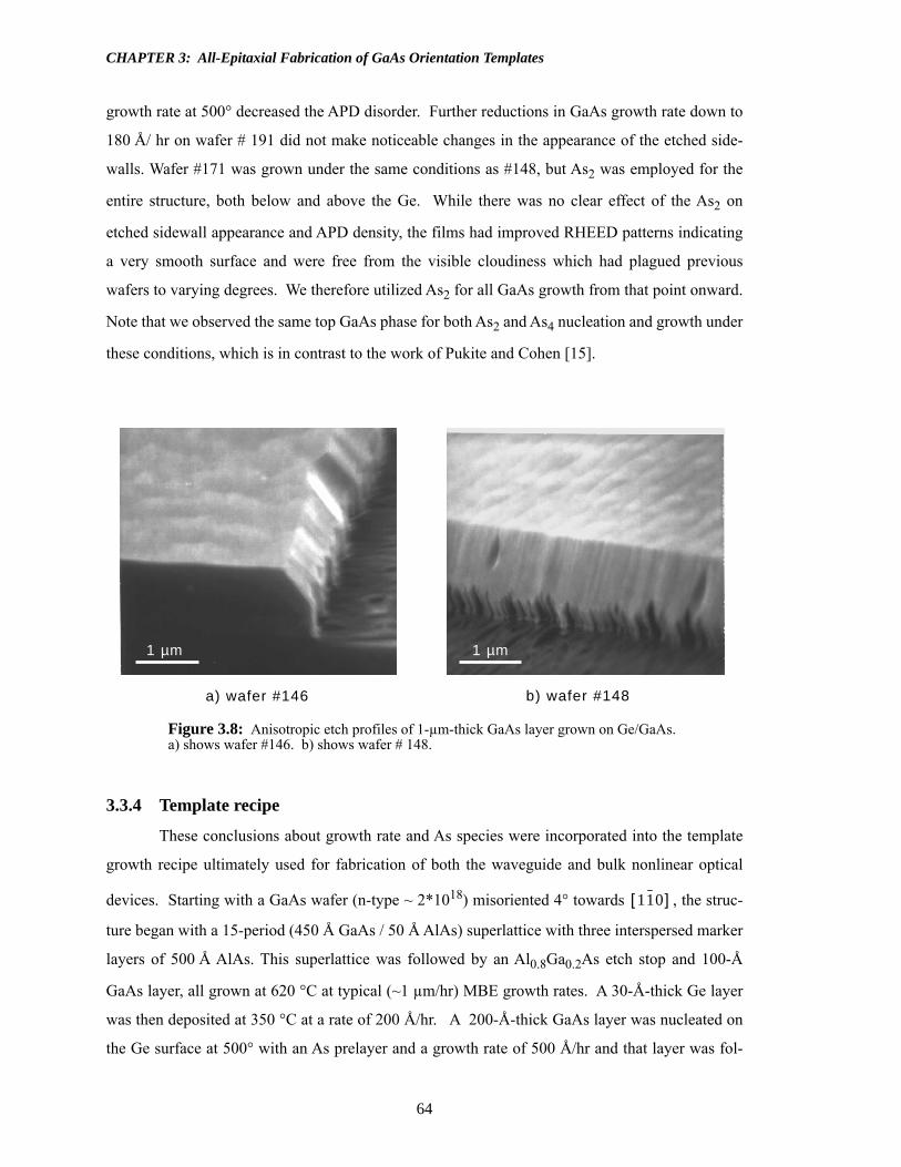
CHAPTER 3: All-Epitaxial Fabrication of GaAs Orientation Templates
64
growth rate at 500° decreased the APD disorder. Further reductions in GaAs growth rate down to
180 Å/ hr on wafer # 191 did not make noticeable changes in the appearance of the etched side-
walls. Wafer #171 was grown under the same conditions as #148, but As2 was employed for the
entire structure, both below and above the Ge. While there was no clear effect of the As2 on
etched sidewall appearance and APD density, the films had improved RHEED patterns indicating
a very smooth surface and were free from the visible cloudiness which had plagued previous
wafers to varying degrees. We therefore utilized As2 for all GaAs growth from that point onward.
Note that we observed the same top GaAs phase for both As2 and As4 nucleation and growth under
these conditions, which is in contrast to the work of Pukite and Cohen [15].
3.3.4 Template recipe
These conclusions about growth rate and As species were incorporated into the template
growth recipe ultimately used for fabrication of both the waveguide and bulk nonlinear optical
devices. Starting with a GaAs wafer (n-type ~ 2*1018) misoriented 4° towards , the struc-
ture began with a 15-period (450 Å GaAs / 50 Å AlAs) superlattice with three interspersed marker
layers of 500 Å AlAs. This superlattice was followed by an Al0.8Ga0.2As etch stop and 100-Å
GaAs layer, all grown at 620 °C at typical (~1 µm/hr) MBE growth rates. A 30-Å-thick Ge layer
was then deposited at 350 °C at a rate of 200 Å/hr. A 200-Å-thick GaAs layer was nucleated on
the Ge surface at 500° with an As prelayer and a growth rate of 500 Å/hr and that layer was fol-
Figure 3.8: Anisotropic etch profiles of 1-µm-thick GaAs layer grown on Ge/GaAs.a) shows wafer #146. b) shows wafer # 148.
a) wafer #146 b) wafer #148
1 µm 1 µm
110[ ]

65
CHAPTER 3: All-Epitaxial Fabrication of GaAs Orientation Templates
lowed by another Al0.8Ga0.2As etch stop. The thickness of the GaAs layer above the Ge was sub-
sequently extended to 1000 Å when it was found that APDs extended up through the layer and
were intersecting the etch stop, causing pitting during template etching. Eventually we placed a
100 Å GaAs cap layer on top of the Al0.8Ga0.2As etch stop to prevent oxidation of the AlGaAs.
The Al0.8Ga0.2As etch stop layer thicknesses varied between 100 Å and 500 Å in various samples.
Further discussion of the etch stops and the complete template structure appears in Section 3.5
after template etching has been described. This epitaxial structure has proved adequate for seeding
orientation-patterned growth of both waveguide and bulk semiconductor devices. The large
(1000Å) residual template corrugations necessitated by the remaining APDs have minimal impact
on thick film growth, but will cause significant scattering problems in waveguide devices.
3.3.5 Further orientation/APB studies
With a workable template technology in place, further investigations into surface prepara-
tion, nucleation conditions and inverted GaAs growth were undertaken to improve the template by
further reducing APD density and lowering the template corrugations. We explored the effects of
different substrate orientations (misoriented toward [110] rather than ), varying nucleation
temperatures, varying prelayer type, and annealing samples at high temperatures before GaAs
nucleation. The experiments are not sufficiently comprehensive to determine an optimal growth
process, but do give significant indications about how best to proceed and demonstrate that better
quality inverted films are possible with lower APD densities. Again, many of these results have
been discussed previously [39], but are reviewed here with the goal of comparing them in more
detail with the literature and drawing conclusions about improving template fabrication processes.
In exploring alternative GaAs nucleation conditions, we cast our net widely. One of the
clear complicating issues in our epitaxial inversion process was the possible uncontrolled presence
of As on the Ge surface before GaAs nucleation, especially since we had no technique available
for characterizing it. Pukite and Cohen observed that high temperature annealing eliminated
adsorbed As from a 1000 Å thick Ge film grown on GaAs. As part of our exploration, we included
high temperature annealing to explore whether such annealing might improve our APD-related
problems. One could imagine it helping in one or both of two ways, either by removing surface As
or by altering the surface step structure to enhance uniform GaAs nucleation. It was unclear, how-
ever, whether such high temperature annealing with a much thinner (100Å) Ge film would pro-
duce clustering. We therefore also performed high temperature annealing with an As flux incident
110[ ]

CHAPTER 3: All-Epitaxial Fabrication of GaAs Orientation Templates
66
on the wafer, as we had previously observed that an incident As flux was effective in stabilizing
thin Ge films against clustering during high temperature annealing. This effect is likely associ-
ated with the observed relative stability of GeAsx surface layers. We had also observed very low
APDs in a few exploratory films which utilized annealing of the Ge surface under an As flux
before GaAs growth, so we decided to explore this effect more systematically. In choosing
annealing conditions and growth temperatures we were guided by the initial work of Ting, et al.
and Sieg, et al. on GaAs/Ge [24, 27].
The exploratory growth process started with growth of a 1000 Å GaAs buffer layer fol-
lowed by 100 Å Ge at the usual 350 °C substrate temperature and 200 Å/hr rate on wafers misori-
ented by 4° towards either [110] or . Next came annealing of the Ge surface at 640°, either
with or without an As flux, after which the wafer temperature was lowered to between 350° and
500° for GaAs nucleation with either an As or Ga prelayer. This prelayer was initiated as soon as
the wafer reached the nominal GaAs growth temperature. The first 10 monolayers of GaAs were
grown by migration-enhanced epitaxy (MEE) at the GaAs nucleation temperature, after which the
temperature was ramped to 500 °C if not already there and 1000 Å GaAs was grown by co-evapo-
ration at 1000 Å/hr. Finally, 9000 Å GaAs was grown at 620 °C at 6000 Å/hr to ensure develop-
ment of a smooth facet during anisotropic etching for examination of the APDs density. The films
were examined by RHEED and by chemical etching with the 1:1:6 etch after lithography.
Table 3.1 summarizes the effects on ultimate GaAs phase of varying the growth parame-
ters. The clearest observation is that the GaAs orientation relative to the Ge depends on nucleation
temperature. The phase of the top GaAs layer is reversed for nucleation above 400 °C vs. below
400 °C whenever the Ge surface is exposed to As before commencing GaAs growth, whether from
the anneal or from the prelayer. The sample nucleated at 397 °C after As exposure is of very poor
quality with huge antiphase domains extending through the 1 µm GaAs film, while the samples
nucleated at 350 °C and 500 °C are much better, with lower APD densities as determined by aniso-
tropic etching. A number of samples of nucleated at temperatures between 350 °C and 500 °C
exhibit APD size and densities that increase with proximity to 397 °C. It appears that there is a
critical temperature around 400 °C at which the top GaAs orientation switches domain. To the
extent examined, the results are consistent on wafers misoriented towards [110] and , as
expected. Additionally, the GaAs phase observed for nucleation at 500 °C is the same as that
observed for the previous template process without annealing or MEE. When growth is nucleated
with a Ga prelayer after annealing without an As flux, such an orientation change with temperature
110[ ]
110[ ]

67
CHAPTER 3: All-Epitaxial Fabrication of GaAs Orientation Templates
is not observed. This observation of opposite phase nucleation at 350 °C on wafer # 363 opens a
new possibility for achieving inversion with [110] misoriented substrates in addition to the previ-
ously developed inversion process utilizing -misoriented substrates and 500 °C nucleation
temperatures. With the greater regularity and smoothness of atomic steps on [110]-misoriented
surfaces compared to misoriented surfaces, it may be possible to achieve lower APD nucle-
ation densities, which would, in turn, make possible thinner template layers and ultimately better
performing waveguide devices.
The effects of simply adding the As2 anneal can be seen in Figure 3.9, which shows the
anisotropically-etched cross-sections of wafers grown under a variety of growth conditions.
Wafers #171 and #177 were grown on -misoriented wafers using our standard template fab-
rication process with 500 °C nucleation and As prelayer followed by co-evaporation of GaAs at
500 Å/hr. The only difference between them is that #177 was annealed for 15 mins at 640 °C
under an As2 flux prior to GaAs growth initiation. No significant change in the APD density
results from the additional anneal. These wafers illustrate our state of the art with templates grown
on -misoriented wafers. Evidence of the APDs begins to appear when we etch to approxi-
mately 1000 Å from the Ge surface. Wafer #167 was grown on a [110]-misoriented wafer with
As-annealing and nucleation at 350 °C using MEE, and has similar APD disruption on the side-
walls as wafers #171 and #177, indicating that a simple switch to [110] misorientation and reduced
growth temperatures doesn’t eliminate APDs, though it does achieve inversion. Wafer #264 is
identical to #167 except that the nucleation and MEE temperature is 425 °C (wafer # 257 at 500 °C
Wafer Anneal Nucleation PrelayerSubstratemisorientation
Tilt of GaAsfilm phase Comments
171 none 500 °C co-evap As 4° to (111)B (111)A (antiphase) template recipe
177 with As 500 °C co-evap - 4° to (111)B (111)A (antiphase) comparable to 171
257 with As 500 °C MEE - 4° to (111)A (111)A (in phase) lower APD density
264 with As 425 °C MEE - 4° to (111)A (111)A (in phase) comparable to 257
283 with As 397 °C MEE - 4° to (111)A mixed very poor quality
167 with As 350 °C MEE - 4° to (111)A (111)B (antiphase) large APDs
303 with As 350 °C MEE - 4° to (111)B (111)B (in phase) no buffer - cloudy
365 w/o As 500 °C MEE As 4° to (111)A (111)A (in phase) lower APDs
363 w/o As 350 °C MEE As 4° to (111)A (111)B (antiphase) lowest APDs
353 w/o As 500 °C MEE Ga 4° to (111)A (111)A (in phase) huge APDs
304 w/o As 350 °C MEE Ga 4° to (111)A (111)A (in phase) lower APDs
Table 3.1: Growth conditions for exploration of orientation and APD dependence.
110[ ]
110[ ]
110[ ]
110[ ]

CHAPTER 3: All-Epitaxial Fabrication of GaAs Orientation Templates
68
behaved similarly, but the pictures didn’t scan well) and we see a significant decrease in the
domain disruption on the etched sidewall, despite the longer etching time. The longer etch time is
clear from the greater overall etch depth. The As anneal appears to have improved the APB quality
only for nucleation temperatures above the 400 °C critical temperature.
Next we examine the impact of the presence and absence of As during the anneal. We can
compare wafer #167 to wafer #363 which had the same growth conditions (anneal 15 mins @
640°; As prelayer and nucleation at 350°) except that # 363 had no As flux incident on the wafer
during the anneal. While there is no impact on the orientation, APD characteristics of # 363 are
much better, with no evidence of APD disruption of the etched facet. This is the single cleanest
etched facet we have seen on any sample. It is more impressive because this sample was deeply
etched, approximately 1 µm into the GaAs underlying the Ge, which means that any APD disorder
present should have propagated a large distance up the facet. Additionally, the top film is clearly
inverted with respect to the substrate, so that this same process could produce an orientation tem-
plate. In this case, the absence of As during the annealing significantly improved the APD quality
of the GaAs film.
For films nucleated above the critical temperature, at 425 °C or 500 °C, the difference
between annealing with and without As is less clear. Wafers #257 (500 °C) and #264 (425 °C)
received an As flux during the 640° anneal, while wafer #365 (350 °C) did not. The wafers have
roughly comparable APD densities and magnitudes, indicating that the As presence during anneal-
ing had less impact for higher temperature nucleation. The high quality of several films annealed
without As indicates that clustering of the 100 Å Ge films during annealing was most likely not a
problem, but this issue was not investigated independently. We observed only that RHEED exam-
ination of the surface after anealing didn’t reveal any signs of 3-D surface features or clustering. It
seems highly unlikely we could have obtained an inverted film, let alone one with the domain
quality of # 363, if any significant mass atomic migration or clustering were occurring during
annealing.
Finally, samples were grown using Ga prelayers instead of As prelayers at both nucleation
temperatures. Obviously, a uniform Ga prelayer is only possible when As is absent during the
annealing step. As Figure 3.9 shows, the sample #304, which had 350 °C nucleation with a Ga
prelayer, is of much better APD quality than sample #353, which had 500 °C nucleation with a Ga
prelayer and contains enormous APDs which even reach the surface in some places.

69
CHAPTER 3: All-Epitaxial Fabrication of GaAs Orientation Templates
Figure 3.9: Etched sample cross-sections showing APD densities for various wafer misorientations and growth conditions.
1 µm
Wafer #363
1 µm Wafer #304 1 µm
Wafer #353
1 µm
Wafer #177
1 µm
Wafer #167
1 µm
Wafer #264

CHAPTER 3: All-Epitaxial Fabrication of GaAs Orientation Templates
70
A number of empirical conclusions can be made from this incomplete data set. Nucleation
using MEE doesn’t change the orientation of the top GaAs film. All samples with Ge surfaces
intentionally exposed to As exhibit an orientation reversal as a function of nucleation temperature.
Annealing under As2 leads to improvements in the APD density only at 500 °C nucleation, while
annealing without As improves APD density for nucleation at 350 °C. Nucleation with Ga yields
better results at 350 °C than at 500 °C and no orientation reversal is observed with temperature.
Overall, we see lower APD densities on several films with [110]-misoriented substrates, As-free
annealing, and 350 °C nucleation, but can’t determine the individual effects of each factor from
the limited set of experiments performed.
3.3.6 Thin buffer exploration
In the interest of fabricating templates using the lift-off process outlined in the introduc-
tion, we also attempted to grow inverted GaAs films using much thinner superlattice buffer layers
under the Ge. When using a lift-off technique, the entire film thickness grown while the mask is in
place contributes to the ultimate template corrugation. Our optimized inversion process on GaAs
wafers misoriented towards described above required a 1-µm-thick GaAs/AlGaAs super-
lattice for smoothing, which would produce a ridiculously large corrugation in the orientation tem-
plate and very poor quality regrown layers. We tried to produce a thinner (~ 500 Å) buffer
structure which would smooth the wafer surface sufficiently to allow growth of Ge and inverted
GaAs with acceptable APD quality on top. We tried thin layer superlattices (50Å GaAs / 30 Å
AlGaAs) and migration enhanced epitaxy, both separately and in combination. Unfortunately, all
attempts to grow inverted GaAs films using these thin buffers on -misoriented wafers
appeared cloudy to the eye, an indication we previously correlated with a high density of antiphase
domains. Note that such a cloudy appearance is only visible once several thousand Ångstroms of
inverted GaAs have been grown. While the APD disorder is present from the initiation of growth
on Ge, only after some amount of GaAs growth does evidence of the resulting surface roughness
become visible to the eye or under an optical microscope. None of the films obtained by this pro-
cess was of sufficient quality for incorporation into a useful template for subsequent regrowth.
The roughening associated with growth on -misoriented wafers is probably responsible for
much of the APD disorder. If epitaxial inversion processes on the generally smoother [110]-mis-
oriented surfaces were perfected, thin buffer structures might become feasible and allow lift-off
template strategies.
110[ ]
110[ ]
110[ ]

71
CHAPTER 3: All-Epitaxial Fabrication of GaAs Orientation Templates
3.4 Epitaxial inversion: Discussion
This section will compare our observations with those of the literature in more detail,
speculate about possible explanations, then make recommendations for future research. There are
three major points of comparison between our work and others’: APD disorder, orientation, and
As-exposure effects.
3.4.1 APD disorder
The results of Strite, et al. [29] are again the easiest to compare with ours with respect to
the antiphase disorder. They report antiphase-domain-free layers from the beginning of growth for
500 °C nucleation with As prelayers on (111)A misoriented wafers. While showing some evi-
dence of 3-D growth initially, their RHEED patterns after 100 Å GaAs growth indicate only a sin-
gle 2 x 4 reconstruction which is highly improved and streaky. Cross-sectional TEM examination
of these films revealed no evidence of APDs. Nucleation under the same conditions but with Ga
prelayers produced a visible density of APD at the GaAs-Ge interface as observed by TEM, a
result which was attributed to incomplete prelayers. In contrast, anisotropic etching of our films
nucleated at 500 °C with As prelayers using wafers reveals a layer of APD defects at the
GaAs-Ge interface. Without the smoothing superlattice, this APD disorder can extend through
1 µm of the GaAs film, while with the buffers it is confined to a region of <1000 Å above the Ge.
We have observed RHEED evidence of APDs during the initial stages of growth and of their anni-
hilation during subsequent growth, but find that anisotropic etching provides much more easily
interpreted results. In contrast, many of our exploratory growths on wafers misoriented towards
[110] have much lower APD densities with only occasional evidence of an APD in the etched
cross-section, even in the absence of any smoothing superlattice. As a result, it is likely that much
of the difference between our results and those of Strite, et al. result from the use of - vs.
[110]-misoriented wafers, which is not surprising given the roughening nature of the GaAs B sur-
face steps. Pukite and Cohen [15] also grew on [110]-misoriented wafers and so may have had
the advantage of the A-step smoothing behavior when they observed APD-free GaAs from the ini-
tiation of growth. Additionally, after growing the 1000-Å-Ge layer, any effects of the underlying
GaAs surface would likely be mitigated by the more isotropically growing Ge.
Ting, et al. [24] also investigated GaAs growth on misoriented and unannealed Ge wafers
containing two-domain surfaces and a majority of single steps. These results were published after
the majority of our investigations into epitaxial inversion were completed, so we did not take
110[ ]
110[ ]

CHAPTER 3: All-Epitaxial Fabrication of GaAs Orientation Templates
72
advantage of them in designing our experiments. RHEED patterns before GaAs growth showed
the mixed 2 x 1 + 1 x 2 surfaces expected from an unannealed bulk Ge surface. However, they
observed dramatic differences between GaAs films when the nucleation temperature was varied
between 350 °C and 500 °C. GaAs nucleated at 500 °C with As prelayers had high APD densities
which varied dramatically across the surface of a single wafer, with some regions having APDs
that annihilated after ~ 1000Å, while other regions had many APDs extending through 1 µm of
GaAs. The variation in size and density of the APDs across the wafer was attributed to disparities
in initial APD nucleation density due to an uncontrolled variable in the experiments, which the
authors suspect is the duration and pressure of the As2 flux. In contrast, films nucleated at 350 °C
had "a conspicuous absence of APDs" as observed by both plan-view and cross-sectional TEM,
exhibiting only a few scattered APDs and none of the huge APDs. Their results point to the poten-
tial importance of the surface As exposure conditions as a factor in determing the quality of the
GaAs film, a topic which will be taken up in more detail in section 3.4.3.
3.4.2 Orientation
For GaAs nucleation at 500 °C on misoriented substrates with no annealing, we see the
same behavior as Strite, et al. [29] growing GaAs/Ge/GaAs heterostructures. They observe GaAs
films in phase with the substrate on [110]-misoriented wafers and we confirm that the GaAs film
orientation follows the Ge surface misorientation, obtaining antiphase films for growth on -
misoriented substrates under the same growth conditions. Their paper doesn’t specify whether As2
or As4 was used for the prelayer, but we observe the same GaAs phase for both As2 and As4
prelayer species for 500 °C nucleation. This independence of prelayer species differs from the
observation of Pukite and Cohen [15], who grew GaAs/Ge/GaAs heterostructures on much thicker
1000Å Ge layers with 500 °C nucleation and observed opposite GaAs phases for nucleation using
As2 and As4 on Ge surface. They observed that exposure to As4 resulted in the two-fold recon-
struction with the electron beam oriented down the Ge surface staircase, while As2 produced a
twofold reconstruction with the beam directed perpendicular to the staircase. Our results with As2
and As4 take the orientation of Pukite’s As4 case, which is the same as the observation of Strite, et
al. Sieg, et al. [27], working with annealed, double-stepped Ge surfaces and nucleating at 350 °C,
observed that As2 and Ga prelayers produced one phase, while As4 prelayers nucleated the oppo-
site phase, again observing domain rotation for the different As species. This differs from our
observation that Ga and As2 prelayers nucleated at 350 °C after high temperature annealing pro-
110[ ]

73
CHAPTER 3: All-Epitaxial Fabrication of GaAs Orientation Templates
duce opposite GaAs phases. Interestingly, Sieg, et al. observe exactly the opposite dependence on
prelayer as Pukite and Cohen, with As2 producing a two-fold reconstruction with the electron
beam oriented down the Ge surface staircase and As4 producing the two-fold looking perpendicu-
lar to the staircase. We unambiguously observe a reversal in GaAs orientation between nucleation
temperatures of 350 °C and 500 °C for As prelayers on annealed Ge layers, which may reconcile to
some degree the apparently contradictory observations of Pukite and Cohen compared to those of
Sieg, et al. regarding As prelayer-initiated growth at 500 °C and 350 °C, respectively. Our results
also appear to be consistent with the results of Koh, et al. [8] who observed GaAs inversion with
Ge buffer layers using -misoriented GaAs wafers nucleated at 580 °C with an As prelayer.
3.4.3 Complications from arsenic exposure
The observed differences in APD and orientation behavior between our results and those
of other researchers may also complicated by unintentional As-exposure of the surface before ini-
tiation of GaAs growth. Both Strite, et al. and Pukite and Cohen report that the Ge surfaces were
As-free before initiation of GaAs growth. In contrast, we had no tools for observing the chemical
composition of the surface (AES or XPS) and reasonably suspect the surfaces contained some As
given the many observations of As segregation during Ge growth on GaAs reviewed in Section
3.2.1. While it might seem that unintentional As exposure of a Ge surface before intentional expo-
sure with an As prelayer would not be important, since a uniform prelayer would be obtained in
either case, there are indications that unintentional As exposure may have additional complicating
effects. These effects go beyond the previously described reversible changes in step structure
upon exposure to an As flux observed in single-stepped Ge surfaces [15].
Unfortunately, there has been very little direct investigation into As-exposed Ge surfaces,
so one can only extrapolate from observations of Si surfaces exposed to As and the chemical simi-
larity of the two materials. Several experiments have found that the surface reconstructions of As-
exposed Ge surfaces depend on temperature and As flux. On Si double-stepped, single-domain
surfaces with adsorbed As, a 2 x 1 reconstruction was observed by RHEED at low temperatures
(< 450 °C) and a 1 x 2 reconstruction was observed at high temperatures (> 600 °C) by Kawabe, et
al. [40]. Becker, et al.[41] observed by scanning tunneling microscopy (STM) a similar reversal
of the surface reconstruction between a 1 x 2 at 400 °C and 2 x 1 at 600 °C, though the observed
reconstructions are opposite of those of Kawabe, et al. for the same temperatures. The detailed
110[ ]

CHAPTER 3: All-Epitaxial Fabrication of GaAs Orientation Templates
74
investigations of Bringans, et al. [42] explain this discrepancy as the result of kinetic limitations
and reveal the complexity of As-exposed Si surfaces.
Bringans, et al. performed a well-controlled series of experiments in which double-
stepped Si surfaces were exposed to As at various temperatues ranging from room temperature to
the approximate As-desorption temperature around 700 °C. They then examined the surfaces by
low energy electron diffraction (LEED) and measured the ratios of the two possible As-Si surface
reconstructions, 1 x 2 and 2 x 1. They observe that the surface reconstruction is a function of the
temperature at which the surface is first exposed to As, with predominantly 1 x 2 observed for ini-
tial exposure temperatures below 350 °C, a mixed reconstruction for temperatures between 350 °C
and 400 °C , and predominantly 2 x 1 for initial exposure temperatures between 400 °C and
600 °C. For first exposure over 650 °C a mixed domain surface is again observed along with As
desorption from the surface. Interestingly, once locked-in at the initial exposure temperature, the
corresponding reconstruction is stable upon annealing up to 650 °C - 700 °C. The explanation
given for this behavior is that while the higher temperature (2 x 1) reconstruction is the lower
energy configuration, kinetic limitations on transformation of the reconstruction and step structure
can preserve the higher energy 1 x 2 reconstruction at higher temperatures. Examining the bond-
ing configuration at the surface, they find that the 1 x 2 surface reconstruction can occur by simple
bonding of As dimers directly on the original double-stepped Si surface, but obtaining the 2 x 1
reconstruction requires rearrangement of the Si surface by mass-migration, since only 1 monolayer
of As is observed on the surface by XPS. This implies that exposure to As between 400 °C and
600 °C catalyzes the migration of half of the surface Si atoms to achieve the 2 x 1 reconstruction,
which has a double-stepped Si surface but with the opposite terrace exposed as the original Si sur-
face. Finally, but perhaps most importantly, they observe that when GaAs is grown on the As-
exposed, double-stepped Si surface, the ultimate GaAs orientation follows the surface reconstruc-
tion set during initial As exposure, independent of the subsequent GaAs nucleation and growth
conditions. The orientation of the GaAs film is thus determined by the As exposure history of the
Si surface, not by the explicit GaAs nucleation and growth conditions.
I discovered the Bringans, et al. reference while preparing this dissertation, so we were not
able to take advantage of its conclusions in the design of our exploratory inversion experiments.
This is unfortunate, in retrospect, because if the Ge surface behaves at all similarly to the Si sur-
face, this model would have made and will in the future make possible much better directed
exploratory growth experiments. Expecting unintentional As exposure of the surface but not sub-
sequent hysteretic behavior of the surface reconstruction with temperature, we took no pains to

75
CHAPTER 3: All-Epitaxial Fabrication of GaAs Orientation Templates
control factors which may turn out to be critical for determining both the orientation and APD den-
sity. The model is, however, immediately helpful for speculatively interpreting our and others’
experimental results. The rotation of the top GaAs phase and our observed critical temperature
could be explained by such As-exposed Ge surface reconstructions. The transition between the
reconstructions could be kinetically limited at these temperatures like Si, or it could be in equilib-
rium and reversible. All the exploratory samples were annealed at 640 °C, some under As flux and
others without an As flux, before cooling to the nominal GaAs nucleation temperatures between
350 °C and 500 °C. Our clear observation of rotation for different nucleation temperatures would
seem to argue for a reversible process rather than a kinetically-limited one, at least in this tempera-
ture range. Note that the same orientation behavior was observed for annealing both with and
without As, so the presence or absence of As at the anneal temperature doesn’t seem to have
changed the dominant reconstruction. The improved domain quality on the As-free annealing
samples might indicate some improved homogenization of the surface reconstruction, but it may
also just reflect [110]-misoriented surface smoothness, as discussed above. Though interpretation
along these lines is appealing, it is important to remember that our surfaces, unlike those of Brin-
gans, et al. had mixed domain terraces and single atomic steps which might behave very differ-
ently than single domain, double-stepped surfaces.
Ting, et al. [24] propose that the As-exposed Ge surface exhibits similar behavior to the
As-exposed Si surface with a transition in the surface structure that occurs around 500 °C. This
proposal is then employed to explain the much higher APD density present in their films grown
around 500 °C, either because the transition is to a mixed domain surface, or because the transition
to a new state was kinetically limited at 500 °C. This explanation could also reconcile the appar-
ently contradictory results of Pukite and Cohen and Sieg, et al. regarding the prelayer dependence
of the final GaAs orientation, since they nucleated at 500 °C and 350 °C, respectively. Clearly,
more knowledge about the behavior of As-exposed Ge surfaces and their temperature-dependence
will be extremely important for intepreting the results of these and future GaAs/Ge growth experi-
ments.
3.4.4 Recommendations
From the results of our experiments and suggestions out of the associated background lit-
erature, we can make some recommendations about how best to proceed in improving the epitaxial
inversion process. The most promising short-term route for improving template fabrication would
involve a combination of [110]-misoriented substrates and 350 °C nucleation. We have demon-

CHAPTER 3: All-Epitaxial Fabrication of GaAs Orientation Templates
76
strated that films grown under these conditions can achieve inversion with relatively low APD
densities, and other research also finds a relative resistance to APD formation for these conditions.
The inherently smoothing properties of type-A steps should be helpful in producing a smooth, uni-
form Ge surface that should assist APD suppression. If successful, this process might allow lift-off
templates with shallow backetching, which would give a very elegant template process and reduce
corrugation amplitudes from those possible in etched template schemes. However, this approach
is finally purely empirical, not one which is based on a fundamental understanding of the factors
controlling inversion or APD formation. Given the probable dependence of the Ge surface step
structure on As exposure conditions and the subsequent dependence of orientation behavior and
APD density on this Ge surface, any real understanding of these processes will require systematic
investigation into the reconstructions and thermal behavior of As-exposed Ge films. Such an
investigation need not reproduce all the detail in the literature regarding As-exposed Si surfaces,
but should determine the dominant reconstructions as a function of thermal and As exposure his-
tory. It could be performed on bulk Ge surfaces originally, where there would be no complications
from unintentional As exposure, then compared to results using Ge films. A number of questions
left unanswered by the literature could be resolved in these experiments, including whether it is
possible to obtain a double-stepped, single-domain reconstruction on a thin Ge film by high tem-
perature annealing or by As-enhanced mass migration effects. Finally, obtaining such a double-
stepped Ge surface is probably the only way to eliminate APD disorder with its deleterious effects
on film morphology and frequency conversion performance, particularly for waveguide devices.
3.5 Template etching
Several features are desirable in the processes used to pattern the inverted GaAs and form
the template. First, it should ultimately allow minimum waveguide corrugation amplitudes to
minimize waveguide losses. In addition, the fabrication process should be scalable from larger
corrugation to very thin corrugation so that one can take advantage of reductions in APD height
without requiring development of a new process. We also need to leave a clean surface in the
trenches and on top of the ridges to achieve high quality MBE regrowth.
These goals must be achieved in the face of several potentially problematic factors. Bulk
measured etch rates are generally given for much deeper etches where the effects of any surface
impurities, non-equilibrium conditions at the beginning of etching, and immersion/removal are
mitigated by the long etching times. Etching of very thin layers (< 1000 Å) can often be unpre-
77
CHAPTER 3: All-Epitaxial Fabrication of GaAs Orientation Templates
dictable and difficult to reproduce. Layers of oxide and other impurities on the wafer can slow the
initial etching rates significantly below the bulk etch rate. Often a definite etch rate can only be
measured after achieving an equilibrium between the various adsorption, reaction, dissolution and
diffusion mechanisms. Immersion and removal effects can also affect shallow etching dispropor-
tionally. Accurate measurement of very thin etch depths is also more difficult than for deeper
etches. Additionally, the presence of APDs at the top GaAs/Ge interface in our template samples
will have unpredictable effects if etching cuts through the GaAs and Ge layers. We observed etch-
ing inhomogeneities such as pinholes and roughened layers on GaAs/Ge/GaAs heterostructures
which were correlated with the height and density of APDs.
Since these problems become more complicated as one tries to etch shallower trenches,
we ruled out simple etching through the GaAs/Ge/GaAs heterostructure as both unscalable to very
small corrugations and unsuitable for producing the smooth surfaces required for regrowth. We
developed two alternative solutions to the patterning problem, one of which utilized masked epi-
taxial growth and another which utilized selective etching and etch stops. We demonstrated both,
but concentrated on the etch-stop solution for reasons which will become clear as the discussion
proceeds.
3.5.1 Lift-off templates
The first approach is to use some kind of in-situ mask to pattern the Ge and overlying
GaAs layers during epitaxial growth. The mask would be placed on or adjacent to the surface so
that epitaxial growth would occur only in the mask openings, after which the mask would be
removed to expose the underlying GaAs substrate. This mask would have micron scale grating
features and would have to be aligned to the GaAs over a wide temperature range to insure that the
Ge and GaAs layers ended up in the right place. In an ideal world, this mask would be removable
in-situ after growth of GaAs/Ge/GaAs so that regrowth could proceed without exposure to atmo-
spheric contamination. Unfortunately, we couldn’t figure out such an in-situ removal scheme, so
we had to rely on ex-situ mask removal and lift-off of the unwanted GaAs/Ge layers. The most
obvious choices for easily depositable, patternable and removable materials compatible with UHV
epitaxial growth are silicon dioxide and nitride. Both dissolve in HF-containing solutions, while
GaAs does not in the absence of an oxidizer like H2O2. With a patterned oxide or nitride layer on
the GaAs surface, epitaxial GaAs grows in the mask trenches while polycrystalline GaAs grows
on the mask surface. This polycrystalline film then needs to be etched away or be lifted-off in con-
junction with removal of the masking layers.
CHAPTER 3: All-Epitaxial Fabrication of GaAs Orientation Templates
78
We made a number of increasingly sophisticated attempts to test the lift-off of these lay-
ers. The first utilized a 1000 Å thick oxide layer which was patterned using photoresist and etching
in 6:1 BOE. After resist removal in acetone, 3-solvent cleaning, and an oxygen plasma descum to
remove carbon, we etched the exposed GaAs for 40 sec using 3:1:50 H3PO4;H2O2:H2O to etch an
approximately 500-Å-deep trench into the GaAs. This rate-limited etch is one of the best for etch-
ing very thin trenches. The goal of this etching was to pre-compensate for the thickness of the
smoothing layers below the Ge and achieve a template with nominally no corrugation. This wafer
was then rinsed and loaded into the MBE chamber where 500 Å of GaAs/AlGaAs were grown by
a combination of MEE and co-evaporation. After removal from the MBE, the liftoff was per-
formed by soaking in 6:1 BOE. We observed that the majority of stripes tended to stick down
instead of lifting off, even when surfactants were added to the BOE. The unsupported polycrystal-
line GaAs films originally deposited on the subsequently dissolved oxide layer were very suscepti-
ble to disintegrating and spreading debris across the wafer. Ultrasonic agitation to encourage lift-
off made this debris problem much worse.
As a result, we tried a different strategy with strained silicon nitride layers. By including
two Si3N4 layers of different strain on top of a SiO2 release layer, we created a structure that would
intrinsically curl up once the SiO2 layer was etched away. This moved the stripe out of the fluid
flow boundary layer next to the wafer and up into the flow where it could easily be flushed away.
Additionally, the polycrystalline GaAs would now be supported on the intact Si3N4 layers to min-
imize any disintegration and associated debris. The liftoff dielectric structure is shown in Figure
3.10 and consisted of 1000 Å of SiO2, 2500 Å of low stress Si3N4, and 3500 Å of tensile-strained
Si3N4. Photolithography was used to define stripes across the surface, after which CF4 plasma
etching was used to etch through the nitride layers and halfway through the oxide layer. Dry etch-
ing was used to preserve the width of the trenches in the dielectric structure which otherwise
would have widened during etching through the Si3N4. To prevent exposure of the GaAs surface
to the flourine-contaning plasma and any associated regrowth complications, we used 6:1 BOE to
etch through the remaining oxide and expose GaAs in the trenches. The sample was prepared for
regrowth in the same way as the oxide samples. In this case the strained nitride layers worked as
expected with virtually all features lifting off except where they were too wide for the 6:1 BOE to
undercut completely in the time allowed. The only undercut lines remaining on the surface were
pinned in place by lithography defects which weren’t undercut completely during the 6:1 BOE
etching. The undercut distance of the 1000 Å SiO2 layer in 6:1 BOE was around 35 µm in the first
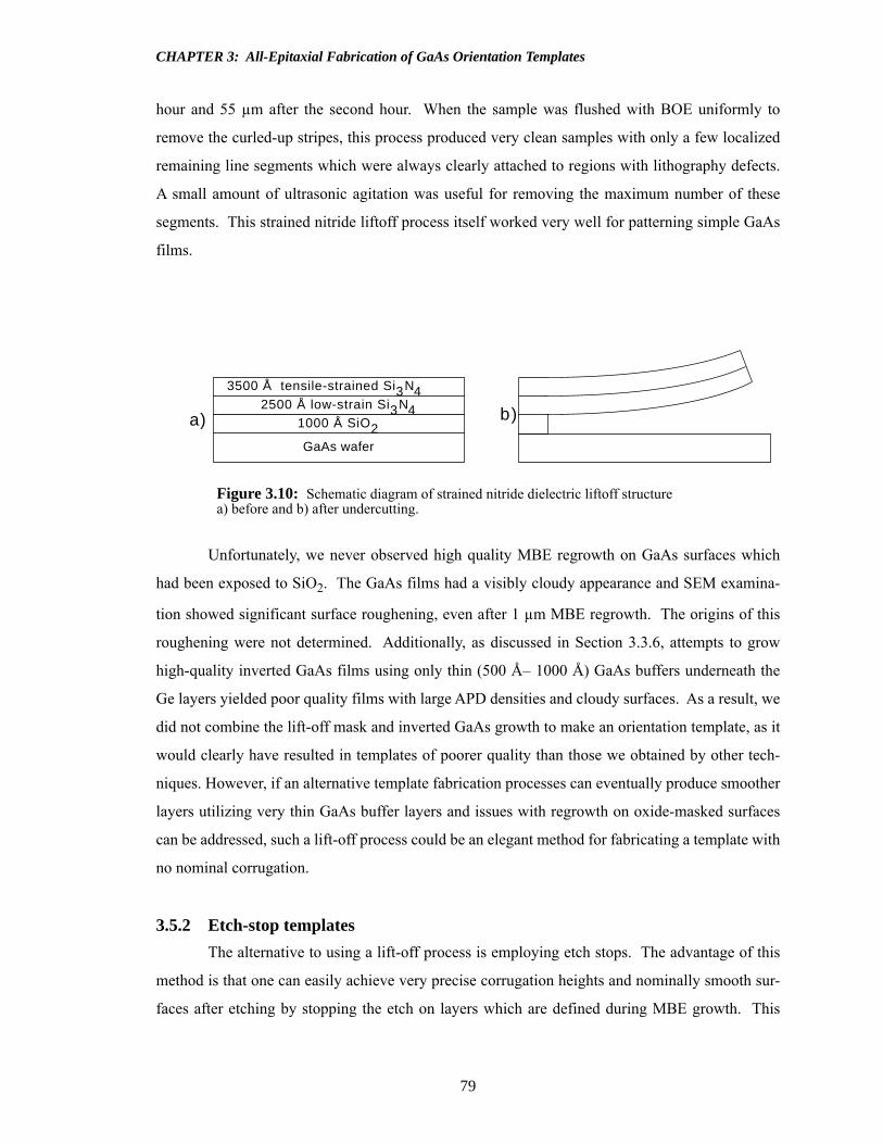
79
CHAPTER 3: All-Epitaxial Fabrication of GaAs Orientation Templates
hour and 55 µm after the second hour. When the sample was flushed with BOE uniformly to
remove the curled-up stripes, this process produced very clean samples with only a few localized
remaining line segments which were always clearly attached to regions with lithography defects.
A small amount of ultrasonic agitation was useful for removing the maximum number of these
segments. This strained nitride liftoff process itself worked very well for patterning simple GaAs
films.
Unfortunately, we never observed high quality MBE regrowth on GaAs surfaces which
had been exposed to SiO2. The GaAs films had a visibly cloudy appearance and SEM examina-
tion showed significant surface roughening, even after 1 µm MBE regrowth. The origins of this
roughening were not determined. Additionally, as discussed in Section 3.3.6, attempts to grow
high-quality inverted GaAs films using only thin (500 Å– 1000 Å) GaAs buffers underneath the
Ge layers yielded poor quality films with large APD densities and cloudy surfaces. As a result, we
did not combine the lift-off mask and inverted GaAs growth to make an orientation template, as it
would clearly have resulted in templates of poorer quality than those we obtained by other tech-
niques. However, if an alternative template fabrication processes can eventually produce smoother
layers utilizing very thin GaAs buffer layers and issues with regrowth on oxide-masked surfaces
can be addressed, such a lift-off process could be an elegant method for fabricating a template with
no nominal corrugation.
3.5.2 Etch-stop templates
The alternative to using a lift-off process is employing etch stops. The advantage of this
method is that one can easily achieve very precise corrugation heights and nominally smooth sur-
faces after etching by stopping the etch on layers which are defined during MBE growth. This
Figure 3.10: Schematic diagram of strained nitride dielectric liftoff structurea) before and b) after undercutting.
GaAs wafer
1000 Å SiO2
2500 Å low-strain Si3N4
3500 Å tensile-strained Si3N4
GaAs wafer
a) b)

CHAPTER 3: All-Epitaxial Fabrication of GaAs Orientation Templates
80
approach mitigates the previously disussed issues of shallow etching and nonuniformities associ-
ated with APDs. Also, it solves a problem caused by the relative etch rates of Ge and GaAs. All
wet etches we investigated (peroxide-based, varying pH from 1 to 14) had significantly higher
etch rates (> 3x) for GaAs than for Ge. The presence of the more etch-resistant layer on top of a
less-resistant layer will produce a "badlands" effect. Small variations in etching through the Ge
layer will cause much larger roughing in the GaAs layer. In general, we found the literature on Ge
wet chemical etching both sparse and often unreliable. By moving to etch-stops we ensured that
the etched trenches would be smooth regardless of the relative GaAs and Ge etch rates. Such etch-
stops could be used in combination with either wet or dry etching processes, though we only used
them with wet etching. Note that selective etching of Ge over GaAs should be possible using fluo-
rine-containing plasmas, but we were reluctant to complicate our fabrication process by involving
another complicated piece of equipment with uncertain operational duty cycle. In principle,
though, use of dry etching could allow extremely thin corrugations and clean surfaces for
regrowth.
Given the sources available in our MBE system, the obvious candidate for etch stops is
clearly high-aluminum-fraction AlGaAs, which has high selectivity in both directions relative to
GaAs using different etch solutions. The more constrained problem of the two is finding a hydro-
gen-peroxide-containing etch that will stop on AlGaAs layers after etching through GaAs and Ge.
Two candidates have been used previously, the NH3OH:H2O2 system and the citric acid:H2O2 sys-
tem. The NH3OH:H2O2 system is very sensitive to pH and only offers limited selectivity [43, 44].
In contract, selectivities of up to 1450 to 1 for etching GaAs over AlAs have been demonstrated
with citric acid/hydrogen peroxide mixtures of 4:1 citric acid: hydrogen peroxide (1:1 citric acid
monohydrate: water by weight; 30% H2O2) [45, 46]. The high selectivity is attributed to the low
solubility of AlxOy in the citric acid solution. The AlGaAs layer oxidizes quickly, but dissolves
slowly, protecting the layers beneath. Carter-Coman discusses complications due to film stress
using this process for thick AlGaAs layers [47], but that is unlikely to be an issue for our desired
thin layers. GaAs etch rates with the 4:1 solution are measured to be ~ 4000 Å/ min, while the Ge
etch rate is on the order of 500 Å/min.
Finding etchants to remove AlGaAs while not etching GaAs is not difficult. Many acids
such as HCl, HF, and H2SO4 will dissolve AlGaAs with aluminum fractions greater than 0.4,
which corresponds roughly to the direct to indirect transition in the bandgap. We chose 1:1
HCl(30%):H2O for template etch stop removal to avoid the complications of using HF solutions.

81
CHAPTER 3: All-Epitaxial Fabrication of GaAs Orientation Templates
Unfortunately, the etch rate is low, around 500 Å/ minute for Al0.7Ga0.3As. The rate can be
increased by adding H2O2 [48], but the addition of an oxidizer enables GaAs etching in the same
solution and so is not suitable for our application. More complicating was the non-uniform disso-
lution across the surface of the wafer. Empirically we found that two process details were neces-
sary for uniform AlGaAs removal. The first was agitation of the etchant or sample by swirling the
beaker. The second was always blowing dry the wafer surface before immersion in the HCl:H2O.
No such dependence on process detail was observed with the citric acid/hydrogen peroxide etch,
which was very robust and always uniform. The color of the wafer surface was always monitored
during AlGaAs removal to check on uniformity. With the proper attention to process detail we
could obtain uniform AlGaAs removal from the surface when viewed either by eye or under a
microscope.
Despite apparently uniform AlGaAs removal, however, strange effects occurred repeat-
edly on nominal GaAs surfaces after removing overlying AlGaAs etch-stop layers. The trenches
looked entirely clear and clean, but after ~ 30 minutes small bright points visible through an opti-
cal microscope would appear across the surface in high density. These points would grow in size
over several days until they could be observed as microscopic faceted crystallites, the density of
which varied dramatically across the surface of a wafer. These particles were present in some den-
sity regardless of the thickness of the AlGaAs layers before removal. Fig 3.11 shows an SEM
micrograph of an etched template with nominally removed AlGaAs and a high density of the
unknown particles on the surface. On template wafers these particles tended to nucleate on the
orientation stripe sidewalls, as seen in Figure 3.11. All attempts to extend etching time or use
alternative etchants (HF, H3PO4, H2SO4) left a similar residue except for boiling H2SO4, which
removed the residue but left a severely pitted wafer surface. Under microscopic observation it
appeared that there was an originally uniform, red-yellow film across the surface of the GaAs
which then coalesced to form the particles, eventually crystallizing, perhaps as the films dried.
When wafers with this contamination were subjected to MBE regrowth, the resulting films suf-
fered from a haziness which varied across the wafer surface. Microscopic examination of the sur-
face revealed enhanced roughness and pitting compared to regrowth on plain GaAs.
We performed XPS analysis of the nominal GaAs surface immediately after overlying
AlGaAs removal to determine the composition of this undesired residual film. The surfaces were
examined by XPS immediately after loading into the vacuum system, then ~ 5 Å of material was
removed from the wafer surface by sputtering with Ar+ before re-examination of the surface by

CHAPTER 3: All-Epitaxial Fabrication of GaAs Orientation Templates
82
XPS. Repeating this removal and examination, we mapped the composition of the near-surface
region as shown in Figure 3.12a. The concentrations were obtained by integrating under the 3p
peaks for various elements. There is a clear enhancement of aluminum and oxygen concentrations
in the near-surface region compared to plain GaAs wafers. It is not clear whether the decrease in
signal with depth is due entirely to sputtering removal of atoms from the surface or whether con-
taminant coalescence into particles might also contribute by reducing the fraction of the surface
covered by Al-O compounds. In either case, however, excess Al and O are clearly present and will
cause regrowth problems, as Al-O compounds, unlike Ga-O and As-O compounds, are not volatile
at typical MBE growth temperatures and so will not desorb from the surface.
Many attempts were made to remove the Al-O scum layer, but the only successful route
found to date resulted from a random conference discussion [49]. Following this suggestion, we
found that a 15 sec dip of the surface into H2O2 after the AlGaAs etch and before drying the film,
followed by another 10 sec dip into HCl was sufficient to remove the contamination layer and
eliminate particle formation. The dip times were not optimized and much shorter times might be
just as effective. XPS depth-profiling analysis of a template surface after the additional H2O2 and
HCl dips is shown in Figure 3.12b.
Here we see no indications of Al above the ~ 5% noise level for our integration time. The
oxygen signal drops very quickly to the noise while the Ga and As signals rise quickly to the
expected 50% values. While we don’t understand precisely the effect of the H2O2 dip, we can
gain some insight by examining the solubility of various Al-oxide and hydroxide compounds.
Table 3.2 shows the solubilities of various Al and O containing compounds in acids and bases.
Figure 3.11: Al-O particles on template surface after nominal AlGaAs removal.
1 µm

83
CHAPTER 3: All-Epitaxial Fabrication of GaAs Orientation Templates
The solubility of the compounds varies widely depending on the exact chemical composition.
Most likely, exposure to H2O2 converts the scum layer from a less soluble composition to a differ-
ent one which is more soluble in HCl. Such a compositional change is also consistent with our
observation that when the surfaces with Al-O contamination films are dipped in H2O2, they no
longer coalesce into particles upon subsequent exposure to air. The H2O2 dip may also oxidize a
layer of GaAs underneath the Al-O layer so that subsequent oxide dissolution in the HCl assists
removal of the aluminum-containing layer from the surface. Our observation of transformation
from a uniform layer to small crystallites over a few days when the films are exposed to air is con-
sistent with similar phase transformations previously observed in aluminum oxide and hydroxide
gel compounds upon drying or hydration. Addition of the H2O2 and HCl dips eliminated the parti-
Figure 3.12: XPS depth profiles of GaAs surfaces after etch stop removal.a) shows enhanced Al and O concentration on samples after AlGaAs removal in HCl.b) shows the same surface with additional H2O2 and HCl dips and dramatically-reduced Al concentration.
0
20
40
60
80
100
0 10 20 30 40 50
atom
ic %
at s
urfa
ce
sputter etch depth (Å)
As
Ga
OAl
0
20
40
60
80
100
0 10 20 30 40 50
atom
ic %
at s
urfa
ce
sputter etch depth (Å)
As
Ga
O
Al

CHAPTER 3: All-Epitaxial Fabrication of GaAs Orientation Templates
84
cle-generating behavior and resulted in our standard wet-etched-template process. Figure 3.13
illustrates the complete structure and the process used to pattern it. The layer thicknesses are rep-
resentative; layer thicknesses varied over the course of template development. As improvements
are made to the APD properties of the inverted GaAs films, the etch-stop layers, the inverted GaAs
layer, and the resultant template corrugations can easily be reduced. In order to ensure a smooth
GaAs surface for subsequent regrowth, we utilized etch stop layers both above and below the Ge
layer. The lower etch stop provides a smooth surface for regrowth in the trenches and deals with
the Ge etch-rate issue, while the upper etch stop and the GaAs cap above it provide sacrificial lay-
ers to keep photoresist and other contamination away from any surface which will be exposed to
MBE regrowth. We found it essential that the top etch stop layer be located above the extent of the
APDs in the inverted GaAs film, which is why the top GaAs layer is ~ 1000 Å thick. Otherwise,
we observed a high density of etch pits across the surface where the etch presumably penetrated
the etch-stop at the APD. The fact that we use a series of selective etches to pattern the template
makes pitting a significant problem, since accidental exposure of the wrong layer at a pit makes
possible dramatic unintended layer undercutting during subsequent etch steps.
hydroxide type composition solubility limit in %
Orthohydroxide
HCl NaOH
cold hot cold hot
alpha Al(OH)3 0.1 0.1 0.4 0.1
beta 4Al(OH)3 - 3H2O 10 0.1 0.4 0.1
gamma Al(OH)3 37 1 insol. 0.1
Polyhdroxide
Dihydroxide 2Al(OH)3 -H2O insol. 5-10 insol. 4
A 4Al(OH)3 --3H2O to
8Al(OH)3 --7H2O
insol. 37 insol. 30
Metahydroxide AlOOH insol insol insol --
table data taken from [50]
Table 3.2: Table of solubilities for aluminum hydroxide compounds
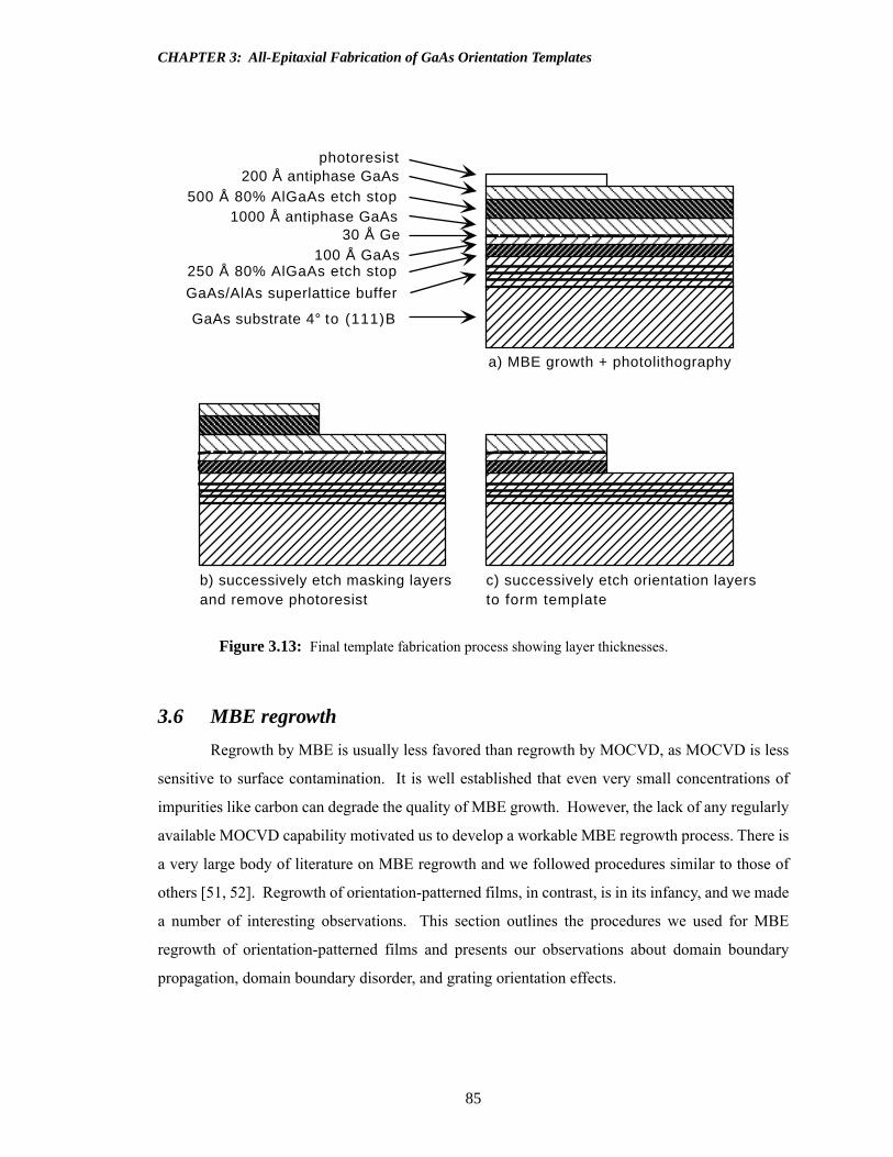
85
CHAPTER 3: All-Epitaxial Fabrication of GaAs Orientation Templates
3.6 MBE regrowth
Regrowth by MBE is usually less favored than regrowth by MOCVD, as MOCVD is less
sensitive to surface contamination. It is well established that even very small concentrations of
impurities like carbon can degrade the quality of MBE growth. However, the lack of any regularly
available MOCVD capability motivated us to develop a workable MBE regrowth process. There is
a very large body of literature on MBE regrowth and we followed procedures similar to those of
others [51, 52]. Regrowth of orientation-patterned films, in contrast, is in its infancy, and we made
a number of interesting observations. This section outlines the procedures we used for MBE
regrowth of orientation-patterned films and presents our observations about domain boundary
propagation, domain boundary disorder, and grating orientation effects.
Figure 3.13: Final template fabrication process showing layer thicknesses.
GaAs/AlAs superlattice buffer
250 Å 80% AlGaAs etch stop
30 Å Ge
200 Å antiphase GaAs500 Å 80% AlGaAs etch stop
100 Å GaAs
1000 Å antiphase GaAs
GaAs substrate 4° to (111)B
photoresist
a) MBE growth + photolithography
b) successively etch masking layersand remove photoresist
c) successively etch orientation layersto form template

CHAPTER 3: All-Epitaxial Fabrication of GaAs Orientation Templates
86
3.6.1 Surface preparation
Typical regrowth surface preparation includes cleaning in a series of hot solvents (trichlo-
roethane, acetone, isopropanol) to degrease and remove any organics from the surface, followed
by a back-etch to remove oxides and contamination. Some groups follow the back-etch by inten-
tional growth of a passivating oxide layer. Detailed discussion about the effects of various etching
[53, 54] and passivation techniques [55, 56] is available. Our only addition to a standard regrowth
preparation was the sacrificial layers on top of the template to protect the GaAs surface from pho-
toresist and atmospheric contamination. Removal of these layers during patterning of the tem-
plates substituted for back-etching. We used a thin AlGaAs etch-stop layer comparable in
thickness to the etch-stop layer underneath the Ge with a thin (100Å) GaAs cap on top to protect
the AlGaAs from oxidation. By placing the photoresist on the top GaAs cap and etching through
the first two (sacrificial) layers, we could then remove the photoresist and perform the solvent
cleaning knowing that the entire surface would be subsequently etched before loading into the
MBE. The sacrificial layers were then etched away in the same steps that cut through the Ge and
removed the underlying AlGaAs etch stop. In this way, all layers exposed to photoresist or sol-
vents are removed before regrowth. Unfortunately, the purity of the citric acid is not as high as
acids such as HCl and it obviously contains carbon, so it may be the source of some impurities
which create roughness and oval defects. We also determined that oxygen plasma ashing of the
sample was necessary to obtain the highest quality regrown films, as regrown GaAs was rougher
in the absence of the oxygen plasma exposure, probably due to carbon contamination. The oxygen
plasma exposure was performed after removal of the photoresist and subsequent 3-solvent clean-
ing, but before the final etching through the Ge layer and underlying etch stop. After etching we
performed a long DI water rinse, then blew the wafers dry and loaded directly into the UHV sys-
tem. We did not use an oxide blow-off before initiating regrowth, as the resulting films appeared
similar with and without the blow-off and we were concerned about potential surface roughening
during extended exposure at high temperature. Regrowth always began with migration-enhanced
epitaxy (MEE), which was intended to bury residual impurities on the surface and help smooth the
surface during the initial stages of growth.
3.6.2 Orientation-patterned regrowth
For nonlinear optical devices, it is necessary that the domain structure be preserved up
though the layers in which the frequency conversion will be performed to obtain the maximum
nonlinear coefficient. This means that the optimal direction for APB propagation will be vertical

87
CHAPTER 3: All-Epitaxial Fabrication of GaAs Orientation Templates
relative to the substrate plane. APBs have been observed to propagate along several different
planes, including {100} and {110} [3]. The energy associated with the incorrect nearest neighbor
bonding for APDs lying in each plane has been estimated by Petroff [57]. From his calculations,
we see that the lowest energy plane for APDs is {110}. This makes some intuitive sense, since an
APD lying in {110} will have an equal number of As-As and Ga-Ga bonds and the APB will be net
charge neutral, unlike APBs lying in other planes. Because {110} is also the cleave plane in GaAs,
it makes sense to orient our waveguide and bulk devices for propagation along <110>, so that we
want the APBs to lie in the {110}. The detailed work of Li [26] found that APDs annihilated with
their APBs in {110} for MOCVD growth in As-rich environments. For MBE growth conditions,
we observed that the APBs propagate approximately in the desired {110} for all the growth condi-
tions we have explored, with temperatures from 450° to 600° and AlGaAs compositions contain-
ing Al fractions from 0% to 70%. We have observed domains with aspect ratios up to 10:1 (5 µm
tall: 0.5 µm wide) grown by MBE. It is clear from research into growth of thick, orientation-pat-
terned GaAs films, discussed in chapter 5, that the APB plane is a function of the growth condi-
tions and particularly the III/V ratio. All our orientation-patterned films were grown under large As
overpressures of approximately 15:1 As/Ga beam equivalent pressures, as is typical for MBE.
Thus, it appears fortunate that typical MBE growth conditions promote APB propagation in {110}
and the vertical domain boundaries required for quasiphasematched frequency conversion devices.
While the domain boundaries themselves grow vertically, faceting at the domain bound-
aries is a significant problem. Figure 3.14 shows the top surface view of a regrown orientation-
patterned GaAs film with clearly visible faceting at the boundaries compared to the surrounding
regions of both orientations. This faceting affects ~ 1 µm on each side of the APB boundary. This
faceting is perhaps not such a problem for widely-spaced boundaries, but for a grating with 2-µm-
wide domains, the coherence length we used for harmonic generation with a 1.55 µm fundamental
wavelength, the disruption affects the entire surface. Needless to say, such disruption is particu-
larly bad for waveguide devices, where any inhomogeneties at the dielectric boundaries will cause
scattering losses.
It is not clear yet whether this faceting results from the growth conditions, or whether it is
generated by defects in the orientation template. Different crystal planes will be exposed at the two
corners of the APB, and it is possible that the different growth rates on these planes or at the APB
itself will produce a faceted surface. For example, inhibited Ga incorporation in the vicinity of the
APD could lead to enhanced growth in nearby regions, thereby creating a groove. Once formed,
such a groove might be subsequently enhanced by diffferences in growth rates on the now existing
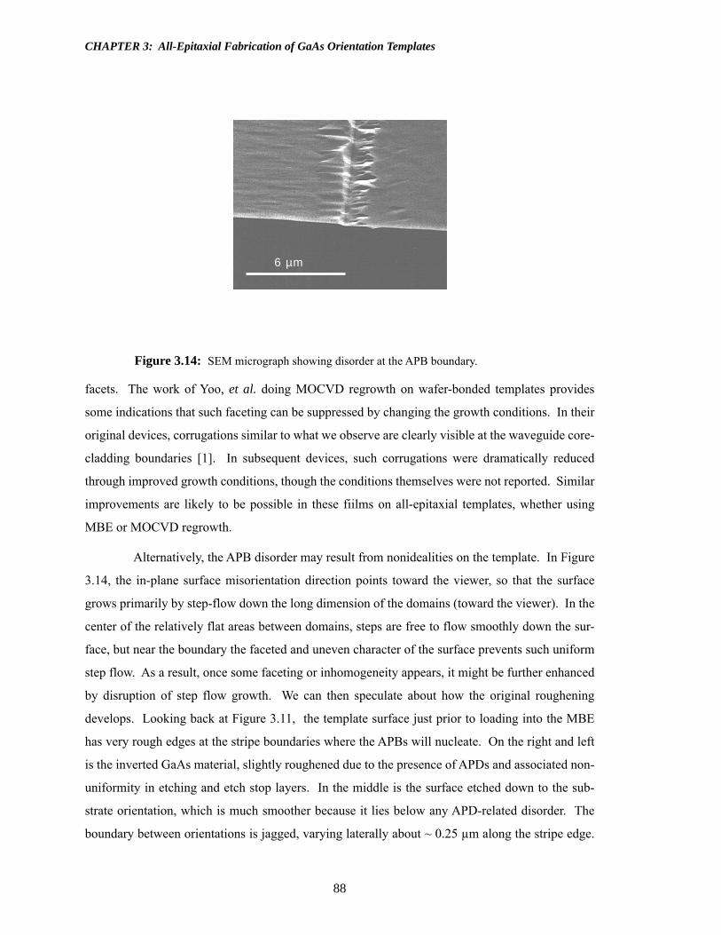
CHAPTER 3: All-Epitaxial Fabrication of GaAs Orientation Templates
88
facets. The work of Yoo, et al. doing MOCVD regrowth on wafer-bonded templates provides
some indications that such faceting can be suppressed by changing the growth conditions. In their
original devices, corrugations similar to what we observe are clearly visible at the waveguide core-
cladding boundaries [1]. In subsequent devices, such corrugations were dramatically reduced
through improved growth conditions, though the conditions themselves were not reported. Similar
improvements are likely to be possible in these fiilms on all-epitaxial templates, whether using
MBE or MOCVD regrowth.
Alternatively, the APB disorder may result from nonidealities on the template. In Figure
3.14, the in-plane surface misorientation direction points toward the viewer, so that the surface
grows primarily by step-flow down the long dimension of the domains (toward the viewer). In the
center of the relatively flat areas between domains, steps are free to flow smoothly down the sur-
face, but near the boundary the faceted and uneven character of the surface prevents such uniform
step flow. As a result, once some faceting or inhomogeneity appears, it might be further enhanced
by disruption of step flow growth. We can then speculate about how the original roughening
develops. Looking back at Figure 3.11, the template surface just prior to loading into the MBE
has very rough edges at the stripe boundaries where the APBs will nucleate. On the right and left
is the inverted GaAs material, slightly roughened due to the presence of APDs and associated non-
uniformity in etching and etch stop layers. In the middle is the surface etched down to the sub-
strate orientation, which is much smoother because it lies below any APD-related disorder. The
boundary between orientations is jagged, varying laterally about ~ 0.25 µm along the stripe edge.
Figure 3.14: SEM micrograph showing disorder at the APB boundary.
6 µm

89
CHAPTER 3: All-Epitaxial Fabrication of GaAs Orientation Templates
These edges have much greater roughness than the photoresist used to mask the etching, so some
other process is responsible for the jagged appearance. The most likely candidate is again the
presence of APDs at the GaAs-Ge interface. When we etch through the APD-containing layer,
there will necesarily be some lateral etching at the stripe edges. Since the citric acid/hydrogen per-
oxide etchant used to remove the GaAs and Ge etches GaAs anisotropically, it will encounter ran-
domly distributed regions of slow and rapid etch rate on the trench sidewalls depending on
whether (111)A or (111)B is exposed. This could easily produce the jagged stripe sidewalls. Sub-
sequent regrowth on a template with such jagged stripe sidewalls will encounter the previously
descibed problems with step flow growth. Smooth step flow growth in the initial stages of growth
near the template APB would be impossible, since this would require nucleation across the wan-
dering APB. While it appears that the APB itself can minimize its energy and relax into a straight
boundary during subsequent MBE growth, the morphological disorder left behind from the nucle-
ation could well be enhanced by subsequent growth. The solution to this problem is again to
reduce the size and density of the APDs at the interface and minimize the amount of non-uniform
lateral etching into the sides of the inverted stripes. APD size reductions will allow thinner tem-
plate layers and reduction of overall etch times and associated lateral etching. Clearly, elimination
of the Al-O particles is also critical to improving these boundaries.
The final issue of orientation-patterned regrowth is the asymmetry between gratings ori-
ented in the two orthogonal directions across the template surface. Figure 3.15 shows an SEM
micrograph of a regrown wafer surface a with 2-µm domain period and the misorientation direc-
tion of the surface parallel to the k-vector of the orientation grating. One can clearly see that the
surface contains relatively large steps every 2 µm. This case is in contrast with Figure 3.14, in
which the grating k-vector was perpendicular to the surface misorientation direction and no step is
visible beyond the simple groove at the APB. When the k-vector and surface misorientation
directions are orthogonal, the domain can grow step flow down the length of a single domain.
When the k-vector and misorientation direction are parallel, however, step-flow growth across the
wafer will repeatedly encounter APBs, across which nucleation of new layers of inverted orienta-
tion will presumably be more difficult. This leads to a pileup of steps at the APBs and the stepped
surface profile of Figure 3.15. We observed the same phenomenena in HVPE growth of thick
GaAs films, with k-vectors parallel to misorientation directions producing films with larger sur-
face roughness and a higher probability of domain overgrowth. Our results indicate that the grat-
ing k-vectors should be oriented perpendicular to the surface misorientation direction to achieve
the smoothest possible layers. Moving to wafers with smaller misorientation angles would also
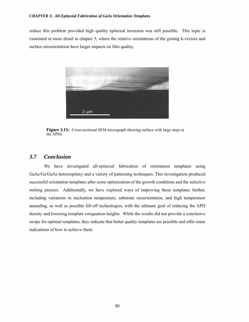
CHAPTER 3: All-Epitaxial Fabrication of GaAs Orientation Templates
90
reduce this problem provided high quality epitaixal inversion was still possible. This topic is
examined in more detail in chapter 5, where the relative orientations of the grating k-vectors and
surface misorientation have larger impacts on film quality.
3.7 Conclusion
We have investigated all-epitaxial fabrication of orientation templates using
GaAs/Ge/GaAs heteroepitaxy and a variety of patterning techniques. This investigation produced
successful orientation templates after some optimization of the growth conditions and the selective
etching process. Additionally, we have explored ways of improving these templates further,
including variations in nucleation temperature, substrate misorientation, and high temperature
annealing, as well as possible lift-off technologies, with the ultimate goal of reducing the APD
density and lowering template corrguation heights. While the results did not provide a conclusive
recipe for optimal templates, they indicate that better quality templates are possible and offer some
indications of how to achieve them.
Figure 3.15: Cross-sectional SEM micrograph showing surface with large steps at the APDs.
2 µm
91
CHAPTER 3: All-Epitaxial Fabrication of GaAs Orientation Templates
References
1. S.J.B. Yoo, R. Bhat, C. Caneau, and M.A. Koza, "Quasi-phase-matched second-harmonic
generation in AlGaAs waveguides with periodic domain inversion achieved by wafer-bond-
ing," Appl. Phys. Lett. 66, 3410-3412 (1995).
2. M.J. Angell, R.M. Emerson, J.L. Hoyt, J.F. Gibbons, L.A. Eyres, M.L. Bortz, and M.M. Fejer,
"Growth of alternating <100>/<111>-oriented II-VI regions for quasi-phase-matched nonlin-
ear optical devices on GaAs substrates," Appl. Phys. Lett. 64, 3107-3109 (1993).
3. N.-H. Cho, B.C. De Cooman, C.B. Carter, R. Fletcher, and D.K. Wagner, "Antiphase bound-
aries in GaAs," Appl. Phys. Lett. 47, 879-881 (1985).
4. P.K. Larsen and D.J. Chadi, "Surface structure of As-stabilized GaAs(001): 2 x 4, c(2 x 8),
and domain structures," Phys. Rev. B 37, 8282-8288 (1988).
5. K. Adomi, S. Strite, H. Morkoc, Y. Nakamura, and N. Otsuka, "Characterization of GaAs
grown on Si epitaxial layers on GaAs substrates," J. Appl. Phys. 69, 220-225 (1991).
6. K. Adomi, S. Strite, and H. Morkoc, "Antiphase-domain-free GaAs grown on pseudomorphic
Si(100) surfaces by molecular beam epitaxy," Appl. Phys. Lett. 56, 469-471 (1990).
7. S. Koh, T. Kondo, T. Ishiwada, C. Iwamoto, H. Ichinose, H. Yaguchi, T. Usami, Y. Shiraki,
and R. Ito, "Sublattice reversal in GaAs/Si/GaAs (100) heterostructures by molecular beam
epitaxy," Jpn. J. Appl. Phys. 37, L1493-L1496 (1998).
8. S. Koh, T. Kondo, M. Ebihara, T. Ishiwada, H. Sawada, H. Ichinose, I. Shoji, and R. Ito,
"GaAs/Ge/GaAs sublattice reversal epitaxy on GaAs (100) and (111) substrates for nonlinear
optical devices," Jpn. J. Appl. Phys. 38, L508-L511 (1999).
9. H. Kroemer, "Polar-on-nonpolar epitaxy: progress and new problems," Inst. Phys. Conf. Ser.
91, 21-26 (1987).
10. M.A. Herman and H. Sitter, Molecular Beam Epitaxy: Fundamentals and Current Status,
Springer Series in Materials Science, U. Gonser, A. Mooradian, K.A. Muller, M.B. Panish,
and H. Sakaki eds. (Springer-Verlag, Heidelberg, 1989).
11. E.H.C. Parker, ed., The Technology and Physics of Molecular Beam Epitaxy (Plenum, New
York, 1985).
12. W. Braun, Applied RHEED: Reflection High-Energy Diffraction During Crystal Growth,
Springer Tracts in Modern Physics (Springer, New York, 1999).
13. X.-S. Wang, K.W. Self, and W.H. Weinberg, "Growth mode of Ge on GaAs(100)," J. Vac. Sci.
Technol. A 12, 1920-1923 (1994).
14. X.-S. Wang, K.W. Self, V. Bressler-Hill, R. Maboudian, and W.H. Weinberg, "Initial stages of
Ge/GaAs(100) interface formation," Phys. Rev. B 49, 4775-4779 (1994).

CHAPTER 3: All-Epitaxial Fabrication of GaAs Orientation Templates
92
15. P.R. Pukite and P.I. Cohen, "Suppression of antiphase domains in the growth of GaAs on
Ge(100) by molecular beam epitaxy," J. Cryst. Growth 81, 214-220 (1987).
16. R.S. Bauer and J.C. Mikkelsen, "Surface processes controlling MBE heterojunction forma-
tion: GaAs(100)/Ge interfaces," J. Vac. Sci. Technol. 21, 491-497 (1982).
17. B.J. Mrstik, "LEED and AES studies of the initial growth of Ge epilayers on GaAs(100),"
Surface Sci. 124, 253-266 (1983).
18. A.D. Katnani, P. Chiaradia, H.W. Sang, P. Zurcher, and R.S. Bauer, "Microscopic effects at
GaAs/Ge(100) molecular-beam-epitaxy interfaces: Synchrotron-radiation photoemission
study," Phys. Rev. B 31, 2146-2156 (1985).
19. F. Stucki, G.J. Lapeyre, R.S. Bauer, P. Zurcher, and J.C. Mikkelsen, "Photoemission study of
GeAs(201): A model for the As-stabilized Ge surface on GaAs/Ge heterojunctions," J. Vac.
Sci. Technol. B 1, 865-870 (1983).
20. J.H. Neave, P.K. Larsen, B.A. Joyce, J.P. Gowers, and J.F. van der Veen, "Some observations
on Ge:GaAs(001) and GaAs:Ge(001) interfaces and films," J. Vac. Sci. Technol. B 1, 668-674
(1983).
21. S.N.G. Chu, S. Nakahara, S.J. Pearton, T. Boone, and S.M. Vernon, "Antiphase domains in
GaAs grown by metalorganic chemical vapor deposition on silicon-on-insulator," J. Appl.
Phys. 64, 2981-2989 (1988).
22. M. Akiyama, Y. Kawarada, and K. Kaminishi, "Growth of single domain GaAs layer on
(100)-oriented Si substrate by MOCVD," Jpn. J. Appl. Phys. 23, L843-L845 (1984).
23. R. Fisher, N.C. Chand, W.F. Kopp, H. Morkoc, L.P. Erickson, and R. Youngman, Appl. Phys.
Lett. 47, 397-399 (1985).
24. S.M. Ting, E.A. Fitzgerald, R.M. Sieg, and S.A. Ringel, "Range of Defect Morphologies on
GaAs grown on offcut (001) Ge substrates," J. Electron. Mater. 27, 451-461 (1998).
25. Y. Li, G. Salviati, M.M.G. Bongers, L. Lazzarini, L. Nasi, and L.J. Giling, "On the formation
of antiphase domains in the system of GaAs on Ge," J. Cryst. Growth 163, 195-202 (1996).
26. Y. Li and L.J. Giling, "A closer study on the self-annihilation of antiphase boundaries in
GaAs epilayers," J. Cryst. Growth 163, 203-211 (1996).
27. R.M. Sieg, S.A. Ringel, S.K. Ting, E.A. Fitzgerald, and R.N. Sacks, "Anti-phase domain-free
growth of GaAs on offcut (001) Ge wafers by molecular beam epitaxy with suppressed Ge
outdiffusion," Jour. Electron. Mater. 27, 900-907 (1998).
28. S. Strite, D. Biswas, N.S. Kumar, M. Fradkin, and H. Morkoc, "Antiphase domain free
growth of GaAs on Ge in GaAs/Ge/GaAs heterostructures," Appl. Phys. Lett. 56, 244-246
(1990).

93
CHAPTER 3: All-Epitaxial Fabrication of GaAs Orientation Templates
29. S. Strite, M.S. Unlu, G.-B. Gao, A. Agarwal, A. Rockett, and H. Morkoc, "GaAs/Ge/GaAs
heterostructures by molecular beam epitaxy," J. Vac. Sci. Technol. B 8, 1131-1140 (1990).
30. S. Strite, D. Biswas, K. Adomi, and H. Morkoc, "Study of sublattice orientation of GaAs on
Ge," J. Appl. Phys. 67, 1609-1612 (1990).
31. C.B. Ebert, "Quasi-phasematched waveguides for infrared nonlinear optics using
GaAs/Ge/GaAs heteroepitaxy," Ph. D. dissertation (Stanford University, Stanford, 1998).
32. M.D. Pashley, K.W. Haberern, and J.M. Gaines, "MBE growth on vicinal GaAs(001) surfaces
studied by scanning tunneling microscopy," Surface Sci. 267, 153-160 (1992).
33. T. Shitara, J. Zhang, J.H. Neave, and B.A. Joyce, "Ga adatom incorporation kinetics at steps
on vicinal GaAs (001) surfaces during growth of GaAs by molecular beam epitaxy," J. Appl.
Phys. 71, 4299-4304 (1992).
34. T. Shitara, D.D. Vvedensky, M.R. Wilby, J. Zhang, J.H. Neave, and B.A. Joyce, "Misorienta-
tion dependence of epitaixal growth on vicinal GaAs(001)," Phys. Rev. B 46, 6825-6833
(1992).
35. A. Poudoulec, B. Guenais, C. D'Anterroches, M. Baudet, and A. Regreny, "Comparative
study of interface structure in GaAs/AlAs superlattices grown by molecular beam epitaxy on
(001) GaAs substrates misoriented towards (111)Ga or (111)As plane," Appl. Phys. Lett. 60,
2406-2408 (1992).
36. N.C. Chand, S.N.G. Chu, and M. Geva, "Effects of substrate misorientation on incorporation
of ambient oxygen and interfacial roughness in AlGaAs/GaAs heterostructures grown by
molecular-beam epitaxy," Appl. Phys. Lett. 59, 2874-2876 (1991).
37. D.C. Radulescu, G.W. Wicks, W.J. Schaff, A.R. Calawa, and L.F. Eastman, "Influence of sub-
strate misorientation on defect and impurity incorporation in GaAs/AlGaAs heterostructures
grown by molecular beam epitaxy," J. Appl. Phys. 63, 5115-5120 (1988).
38. P.M. Petroff, R.C. Miller, A.C. Gossard, and W. Wiegmann, "Impurity trapping, interface
structure, and luminescence of GaAs quantum wells grown by molecular beam epitaxy,"
Appl. Phys. Lett. 44, 217-219 (1984).
39. C.B. Ebert, L.A. Eyres, M.M. Fejer, and J.S. Harris, "MBE growth of antiphase GaAs films
using GaAs/Ge/GaAs heteroepitaxy," J. Cryst. Growth 201, 187-193 (1999).
40. M. Kawabe, T. Ueda, and H. Takasugi, "Initial stage and domain structure of GaAs grown on
Si(100) by molecular beam epitaxy," Jpn. J. Appl. Phys. 26, L114-L116 (1987).
41. R.S. Becker, T. Klitsner, and J.S. Vickers, "Arsenic-terminated silicon and germanium sur-
faces by scanning tunneling microscopy," J. Microsc. 152, 157-165 (1988).

CHAPTER 3: All-Epitaxial Fabrication of GaAs Orientation Templates
94
42. R.D. Bringans, D.K. Biegelsen, and L.E. Swartz, "Atomic-step rearrangement on Si(100) by
interaction with arsenic and the implication for GaAs-on-Si epitaxy," Phys. Rev. B 44, 3054-
3063 (1991).
43. J.J. LePore, "An improved technique for selective etching of GaAs and Ga1-xAlxAs," J. Appl.
Phys. 51, 6441-6442 (1981).
44. R.A. Logan and F.K. Reinhart, "Optical waveguides in GaAs-AlGaAs epitaxial layers," J.
Appl. Phys. 44, 4172-4176 (1973).
45. M. Tong, D.G. Ballegeer, A. Ketterson, E.J. Roan, K.Y. Cheng, and I. Adesida, "A compara-
tive study of wet and dry selective etching processes for GaAs/AlGaAs/InGaAs Pseudomor-
phic MODFETs," Jour. Electron. Mater. 21, 9-15 (1992).
46. H.G. Lee, M.S. Tse, K. Radhakrishnan, K. Prasad, J. Weng, S.F. Yoon, X. Zhou, H.S. Tan,
S.K. Ting, and Y.C. Leong, "Selective wet etching of a GaAs/AlxGa1-xAs heterostructure with
citric acid-hydrogen peroxide solutions for pseudomorphic GaAs/AlxGa1-xAs/InyGa1-yAs
heterojunction field effect transister [sic] fabrication," Mater. Sci. Eng. B 35, 230-233 (1995).
47. C. Carter-Coman, R. Bicknell-Tassius, R.G. Benz, A.S. Brown, and N.M. Jokerst, "Analysis
of GaAs substrate removal etching with citric acid:H2O2 and NH4OH:H2O2 for application to
compliant substrates," J. Electrochem. Soc. 144, L29-L31 (1997).
48. K. Bacher and J.S. Harris, "A wet etching technique for accurate etching of GaAs/AlAs dis-
tributed Bragg reflectors," J. Electrochem. Soc. 142, 2386-2388 (1995).
49. P. Moran, personal communication to J.S. Harris (1998).
50. Gmelins, Aluminium Teil B: Die Verbindungen des Aluminiums, Gmelins Handbuch der
Anorganischen Chemie (Verlag Chemie, Berlin, 1934).
51. H.P. Meier, E. Van Gieson, W. Walter, C. Harder, M. Krahl, and D. Bimberg, "Molecular
beam epitaxy of GaAs/AlGaAs quantum wells on channeled substrates," Appl. Phys. Lett. 54,
433-435 (1989).
52. J.S. Smith, P.L. Derry, S. Margalit, and A. Yariv, "High quality molecular beam epitaxial
growth on patterned GaAs substrates," Appl. Phys. Lett. 47, (1985).
53. Z.H. Lu, C. Lagarde, E. Sacher, J.F. Currie, and A. Yelon, "A surface analytical study of
GaAs(100) cleaning procedures," J. Vac. Sci. Technol. A 7, 646-650 (1989).
54. J. Massies and J.P. Contour, "Substrate chemical etching prior to molecular-beam epitaxy: An
x-ray photoelectron spectroscopy study of GaAs {001} surfaces etched by the H2SO4-H2O2-
H2O solution," J. Appl. Phys. 58, 806-810 (1985).
55. J.P. Contour, J. Massies, H. Fronius, and K. Ploog, "An XPS study of the passivating oxide
layer produced on GaAs (001) substrate by heating in air above 200°C," Jpn. J. Appl. Phys.
27, L167-L169 (1988).

95
CHAPTER 3: All-Epitaxial Fabrication of GaAs Orientation Templates
56. J. Saito, N. Kazuo, T. Ishikawa, and K. Kondo, "GaAs surface cleaning by thermal oxidation
and sublimation in molecular-beam-epitaxy," J. Appl. Phys. 63, 404-409 (1988).
57. P.M. Petroff, "Nucleation and growth of GaAs on Ge and the structure of antiphase bound-
aries," J. Vac. Sci. Technol. B 4, 874-877 (1986).

CHAPTER 3: All-Epitaxial Fabrication of GaAs Orientation Templates
96
97
CHAPTER 4: Fabrication and Characterization of Orientation-Patterned Waveguide Devices
The first nonlinear optical frequency conversion devices we investigated were orientation-
patterned AlGaAs waveguide devices. These first devices were strip waveguides suitable for
WDM frequency shifting, although they were characterized using simpler second harmonic gener-
ation experiments. After an introduction to nonlinear optical waveguide devices, this chapter will
describe the design of the devices, their fabrication, and finally the evaluation of their optical prop-
erties, both linear and nonlinear. The chapter closes with a discussion of the present limitations on
these devices and strategies for reducing the performance-limiting waveguide losses. Some of the
results have been previously published in [1].
4.1 Introduction
Waveguide nonlinear-optical-frequency-conversion devices have advantages over bulk-
focused devices for some applications. Since the propagation is determined by a dielectric struc-
ture rather than diffraction, one can achieve a tightly focused spot over long device lengths and
achieve orders of magnitude higher gain. This higher gain makes possible high conversion effi-
ciencies at much lower pump powers than with bulk-focused devices (~ 103 as derived in Chapter
2). In particular, nonlinear optical waveguides are well-suited to the powers obtainable from sin-
gle-stripe diode lasers (~ 10s to 100s of mW). The suitability of diode lasers as pumps offers
potentially compact, robust, and efficient nonlinear optical systems. One eventual dream for fre-
quency conversion in semiconductors would be to integrate monolithically the pump diode/s and
the nonlinear waveguides on the same substrate to achieve the ultimate in size, robustness and
packaging simplicity.
However, accompanying these efficiency advantages come some limitations. The most
obvious of these is the inherent limitation on power handling due to the small area of the
waveguide endfacet and the finite optical damage threshold of the material. A more subtle compli-
cation is the necessarily multi-moded nature of nonlinear optical waveguides. Since any three-fre-
quency interaction requires that two of the wavelengths involved differ by at least a factor of two,
a typical dielectric waveguide will support multiple transverse modes at one or more of the rele-
vant frequencies. So long as only wavelengths where the guide is single-moded are coupled into

CHAPTER 4: Fabrication and Characterization of Orientation-Patterned Waveguide Devices
98
the waveguide and the shorter wavelength modes are generated in the guides, as in SHG, this is not
usually a significant problem. When shorter wavelength pump radiation must be coupled into the
multi-moded waveguides, as is the case for some WDM mixer configurations and for all mid-IR
generation devices, things become more complicated. Some fraction of the input power is coupled
into modes other than the desired one, usually the lowest order transverse mode; this sensitive cou-
pling reduces the effective pump power driving the frequency conversion process and makes the
overall device extremely sensitive to mechanical stability, since slight misalignment of the input
beam redistributes the input power among the waveguide modes.
By examining the present state of the art in waveguide nonlinear optical devices, one can
gain an idea where semiconductor waveguides would be useful. The most widely and successfully
used nonlinear optical waveguide fabrication process to date has been the annealed proton
exchange (APE) in periodically-poled lithium niobate (PPLN) [2, 3]. The first major area of
APE:PPLN application has been for optical communication system devices where the absolute
power levels are constrained by propagation through optical fibers and where issues of cost neces-
sitate diode laser pumps. Examples of such applications include wavelength shifting for conver-
sion between WDM channels [4-6], mid-span spectral inversion for dispersion compensation [7],
all-optical switching [8, 9], and time-division multiplexing [10]. For these applications, semicon-
ductor devices could offer higher efficiency conversion at lower pump power levels and also offer
straightforward polarization-independent wavelength conversion [11] simply by proper selection
of pump polarization [12]. Another important APE:PPLN application where semiconductors
would offer advantages is mid-IR generation for spectroscopic applications. Difference frequency
generation of two diode lasers has been used to generate tunable mid-IR radiation for molecular
spectroscopy [13, 14]. The much wider transparency range of semiconductors could allow such
mid-IR generation out to the 12 µm wavelength range, much further than is possible with ferro-
electric materials. For both of these applications, one of the critical breakthroughs for realizing
efficient device performance was finding a solution to the previously mentioned higher-order
mode coupling problem using tapered waveguides and integrated directional couplers [15].
In semiconductor waveguides, many techniques other than QPM have been used to phase-
match frequency conversion and take advantage of semiconductors’ favorable characteristics,
though none has yet proven clearly superior. Boyd proposed modal phasematching for optical
parametric oscillators in AlGaAs waveguides, though the devices have poor mode overlap and
very high thresholds [16]. Van der Ziel and coworkers demonstrated form-birefringent phase-
matching in AlGaAs superlattice waveguides, but the birefringence obtainable by this technique
99
CHAPTER 4: Fabrication and Characterization of Orientation-Patterned Waveguide Devices
( ) is not sufficient to phasematch most of the interesting device applications
[17]. Oxidation of high Al-fraction AlGaAs in similar superlattices has recently provided an alter-
native technique which offers sufficient birefringence ( ) for phasematching useful
interactions. Harmonic generation of a 1.5 µm laser was demonstrated in such an oxidized multi-
layer with ~8 dB/cm loss around 1.55 µm, but it was limited in efficiency by the 2000 dB/cm loss
at the harmonic wavelength [18]. Mid-IR generation experiments were similarly limited by high
losses of 217 dB/cm at the long wavelength [19, 20].
Spatial modulation of the magnitude of the nonlinear susceptibility in GaAs/AlGaAs
superlattices after epitaxial crystal growth has been accomplished by two techniques. Impurity-
free vacancy disordering has produced a 17% modulation in the magnitude of the nonlinear sus-
ceptibility with sufficient resolution to allow first-order quasiphasematching of 1.55 µm-pumped
frequency doubling [21]. Losses reported for waveguides fabricated with this techniques are ~
8 dB/cm [22]. Ion implantation techniques have also been used to modulate the nonlinear suscep-
tibilities of asymmetric quantum well waveguides [23, 24], but measured susceptibilities in the
near-IR wavelength range were small. Semiconductor surface emitting devices were also explored
with phasematching obtained in the vertical direction by modulation of the waveguide core com-
position and/or resonant enhancement from a vertical cavity [25-27], but the non-collinear propa-
gation inevitably limits the obtainable conversion efficiency.
By far the most impressive waveguide device results in semiconductors have been
obtained by Yoo and coworkers at Bellcore. They demonstrated both SHG [28] and WDM channel
shifting in AlGaAs waveguides [12] regrown on wafer-bonded template structures. Devices had
waveguide losses of 5 dB/cm at 1550 nm and 25 dB/cm near 750 nm which limited the conversion
efficiency of the wavelength conversion to -19 dB. Despite the high losses at short wavelength,
such devices were used to demonstrate functions such as polarization filtering [29], spectral inver-
sion, and multi-channel conversion. The waveguiding layers were grown using two MOVPE
regrowth steps to produce fully buried heterostructures with more symmetric modes and better
coupling efficiencies to fibers.
∆nTE TM– 0.033=
∆nTE TM– 0.6=

CHAPTER 4: Fabrication and Characterization of Orientation-Patterned Waveguide Devices
100
4.2 Waveguide Design
For initial demonstration of orientation-patterned waveguide devices, it was unclear which
factors would limit the performance, though we anticipated that high waveguide losses were
likely. As a result, we focused our design primarily on ease of fabrication and testing, leaving
issues of noncriticality and mode coupling to fibers for a later time when the limitations would be
better understood. Initial design choices were made according to fundamental considerations,
after which more detailed numerical calculations were used to predict efficiencies and tuning
behavior.
4.2.1 Considerations and constraints
One of the most important considerations for waveguide design is for the devices to be
single-transverse-moded to simplify mode launching. At the same time, the mode needs to be suf-
ficiently large to allow decent endfire coupling efficiency at reasonable numerical aperture. Ulti-
mately, tapered waveguides like those used in APE PPLN devices would allow independent
optimization of input coupling and QPM regions, but for the current devices both of these must be
accomplished within the constraints of epitaxial growth and lithographic patterning of a single
MBE-grown structure. For MBE, layer thickness is limited pratically to a maximum of between
5 µm and 10 µm depending on composition and grower disposition. For lithography, we observed
that photoresist stripes with linewidths < 3 µm suffered much higher rates of delamination across
typical wafers, an issue that could certainly be improved with optimized lithographic processes,
but which constrained our waveguide widths in devices fabricated to date. Another constraint is
that doing a second regrowth to form a completely buried heterostructure was not feasible, both
because of the additional demand placed on the MBE system, and because MBE regrowth on Al-
containing layers does not produce good quality layers. Aluminum oxides, which will form when
AlGaAs layers are exposed to air, are not volatile at temperatures compatible with GaAs and
MBE. Thus, the growing layers will nucleate on the amorphous oxide surface rather than a clean
semiconductor surface, resulting in significantly degraded material quality. With access to
MOVPE regrowth capability, this constraint would be relaxed and buried heterostructure devices
could be fabricated as demonstrated by Yoo and coworkers [12]. As a result, we must fabricate the
device with a single growth of a vertical waveguide structure followed by some etching step to
provide lateral confinement. The vertical transverse mode properties will thus be dominated by
the epitaxial structure, while the lateral transverse mode properties will be determined by a combi-
nation of the epitaxal structure and the etching profile.

101
CHAPTER 4: Fabrication and Characterization of Orientation-Patterned Waveguide Devices
The composition of the waveguide core was selected so that the device would be transpar-
ent at the harmonic wavelength around 775 nm for a fundamental 1.55 µm pump laser. The band-
gap of AlxGa1-xAs as a function of Al fraction exhibits a sharp discontinuity at the transition
between the direct and indirect transition, so that the increase in bandgap with Al composition is
much lower above x = 0.45. We chose an Al0.5Ga0.5As core to insure transparency and low resid-
ual bandtail absorption at the short wavelength. To determine the remaining parameters for the
waveguide including core thickness, cladding thicknesses, and cladding composition, we can refer
to the results derived in Section 2.2.3. Since we will be utilizing diffusion-limited wet chemical
etching and we will need to etch through both the top cladding and the core to achieve our desired
degree of lateral confinement, we choose a cladding composition of Al0.6Ga0.4As so that the etch-
ing rates of the core and cladding will not differ too significantly. Choosing a smaller core-clad-
ding composition difference is also possible, but would require core and cladding of
correspondingly greater thickness. We see from Figure 2.4 that a normalized top cladding thick-
ness equal to the core thickness ( ) will yield an approximately symmetric mode for normal-
ized confinements .
The thickness of the lower cladding is also important to prevent excessive radiation losses
from the waveguide core into the substrate, since the waveguide core layer will have a refractive
index lower than the GaAs substrate. We can estimate the leakage into the substrate by the pertur-
bation technique of Stultius and Streifer [30], approximating our 4-layer structure with as
a symmetric 3-layer waveguide on a high index substrate. They first calculate the modes of the
structure in the limit that the lower cladding is infinitely thick, then perturb the eigenvalue equa-
tion with to calculate a correction to the mode index when the lower cladding is
finite. They derive an expression for the perturbed TE mode index .
(4.1)
where
(4.2)
(4.3)
(4.4)
(4.5)
(4.6)
from which we can calculate the power attenuation in dB
w 1=
V 1.7≥
w 1=
β β∞ δβ+=
δβ 2k22k3
k4 ik3–k4 ik3+------------------
2k3t3–( )exp
β∞teff k22 k3
2+( )----------------------------------=
teff t2 1 k1⁄ 1 k3⁄+ +=
k1 β2 k02n1–( )1 2⁄
=
k2 k02n2 β2–( )1 2⁄
=
k3 β2 k02n3–( )1 2⁄
=
k4 k02n4 β2–( )1 2⁄
=
CHAPTER 4: Fabrication and Characterization of Orientation-Patterned Waveguide Devices
102
(4.7)
Originally we used lower-cladding layers of 2-µm thickness, but found that this planar
leakage model predicts 5 dB/cm losses. A cladding layer of 3 µm for these waveguide composi-
tions and 1 µm core thickness will serve to reduce losses below the 0.21 dB/cm level. This calcu-
lation is only for TE modes, but for our SHG devices the TM mode will be at the harmonic
wavelength and the radiation losses will be negligible. The total thickness of the waveguiding lay-
ers is thus 5 µm, to which we will add a 1 µm thick superlattice buffer layer before the waveguid-
ing layers to smooth the surface before waveguide growth. Our vertical waveguide structure is
thus like that of Yoo and coworkers [28], allowing direct comparison with their results.
Lateral confinement will be achieved by etching through a planar waveguide structure.
Sufficient confinement to make the waveguide single-moded in the horizontal direction can be
obtained over a range of rib widths, since we can trade rib width vs. etch depth to yield the same
normalized confinement. However, one important consideration pushes us in the direction of deep
etching. Practically, coupling of the fundamental radiation into the ridge waveguide is greatly sim-
plified by insuring that the surrounding planar waveguide is cut-off at the fundamental wave-
length. Input coupling and observation of the desired mode is much easier when not complicated
by a background of radiation transmitted through the planar waveguide. The desirabiliy of this cri-
terion was determined empirically by working with waveguides of both designs. This is particu-
larly true when one examines devices with short lengths where the planar mode radiation has little
distance over which to diffract in the plane.
Unfortunately, the case where lateral cladding is formed by etching a planar waveguide to
or beyond cutoff is the most complicated case to model. For very weak confinement, one can use
the effective index approximation [31] (and references therein) to estimate the degree of lateral
confinement, but as the planar region approaches cutoff this method diverges from the actual solu-
tion [32]. Below the planar mode cutoff, no mode index exists to use in the approximation. To
allow comparision between theory and experiment we therefore modeled this device using a
numerical 2-D finite-difference-equation (FDE) analysis described in the next section.
α dB/cm( ) 8.68Im δβ( )34.7k2
2k32k4
k42 k3
2+--------------------------
2k3t3–( )exp
β∞teff k22 k3
2+( )----------------------------------= =

103
CHAPTER 4: Fabrication and Characterization of Orientation-Patterned Waveguide Devices
4.2.2 Finite difference equation (FDE) modelling
To predict the efficiency and tuning behavior of this waveguide device we utilized a
numerical FDE solution for quasi-TE and quasi-TM modes implemented using Matlab. The
method follows that described by Stern [33, 34]; our implementation was compared to the test
cases contained in these papers to an accuracy in the modal index of approximately 2*10-4. Since
the waveguide mode is always symmetric or antisymmetric about the center of the waveguide, we
modeled only half of the mode to minimize computational time. Figure 4.1 shows the FDE-
solved, lowest-order fundamental and harmonic modes of the previously described waveguide
structure with vertical sidewalls. Using this model, we can obtain the results shown in Figure 4.2
for the harmonic generation effective area as a function of etch depth and waveguide width for the
vertical structure described above. The transition to double-moded behavior is shown by the
approximately horizontal dotted line. This line is approximate, as the FDE solver loses accuracy
as the waveguide mode approaches cutoff and the mode extends much further from the core
region. The vertical dashed line shows the etch depth required for achieving cutoff of the planar
mode. By placing stripes of widths ranging from 3-8 µm on the waveguide mask, we can ensure
that at least some of the devices will be single-moded. This allows for some variability in the etch-
ing process, as well as some in the undercut which will occur for isotropic etches and which will
reduce the waveguide width an amount comparable to the etch depth on each side. The actual
Figure 4.1: Fundamental and harmonic modes of FDE-modelled ridge waveguidesconsisting of air/Al0.6Ga0.4As/Al0.5Ga0.5As /Al0.6Ga0.4As layers with 1-µm-thick coreand top cladding layers and 5 µm stripe width. Contours are in increments of 10% ofthe peak field amplitude.

CHAPTER 4: Fabrication and Characterization of Orientation-Patterned Waveguide Devices
104
range of apparent single mode behavior will be wider than that marked by the dashed line, since
higher order modes near cutoff will have high modal fields at dielectric boundaries and therefore
suffer from very high waveguide losses.
4.3 Orientation-patterned waveguide fabrication
Our orientation-patterned waveguide devices were fabricated using a combination of
MBE to grow a planar waveguiding layer and wet chemical etching to provide lateral confine-
ment. There is a large literature on semiconductor waveguide fabrication of which some examples
are available in [35] and [36].
4.3.1 MBE regrowth of waveguide structures
The channel waveguide devices were fabricated by the epitaxial inversion/patterned
regrowth technique described in Chapter 3. After regrowth preparation, waveguiding layers were
grown by MBE. A GaAs/AlGaAs superlattice buffer identical to that used in Chapter 3 was grown
on the template before growth of the waveguiding layers. This buffer is useful because regions of
the surface clearly have B-type steps exposed and we expect roughening similar to that observed
Figure 4.2: Effective area of etched-rib waveguides for second harmonic generationusing a 1.55 µm fundamental as a function of rib width and etch depth. Vertical lineshows cutoff for planar waveguide mode. Approximately horizontal line shows limitof single-mode transverse behavior
0
2
4
6
8
1 0
1 2
0 0.2 0.4 0.6 0.8 1
effe
ctiv
e ar
ea (
µm2)
etch depth
3 µm
4 µm
6 µm
8 µm
planar modeabove cutoff
planar modebelow cutoff
rib width

105
CHAPTER 4: Fabrication and Characterization of Orientation-Patterned Waveguide Devices
on the much cleaner -misoriented wafers. In the absence of those buffers, the regrown film
regions are much rougher. The exact composition of the superlattice layers is most likely not sig-
nificant, so that the compositions can be adapted to be compatible with the growth rates set for the
cladding and core layers. After the superlattice buffer, the waveguide cladding was grown, fol-
lowed by the core and top cladding layers. Typical regrowth rates were 0.5 µm/hour with two dif-
ferent Ga sources, with one flux set for the core composition and the other flux set for the
difference between the core and cladding compositions.
A cleaved and stain-etched SEM cross section of the waveguide structure grown by the
above process is shown in Figure 4.3. After cleaving, the sample was stain-etched in a potassium
ferricyanide solution to reveal the domain boundaries and composition differences. The exposed
surface is misoriented towards the in-plane , so that the grating k-vector lies along [110] and
we have no macroscopic “stair-stepping” of the surface. The APBs can be clearly seen running
almost perfectly vertically up through the GaAs, superlattice, and AlGaAs layers. In the region of
vertical propagation, the APBs lie in or approximately in {110}. This vertical propagation was
observed under all growth conditions examined, with compositions from GaAs to 70% AlGaAs,
growth temperatures from 450 °C to 600 °C, and varying growth rates. Some authors have
hypothesized [37] that APB propagation plane is a function of the vapor concentrations above the
substrate. If there were some dependence of the APB propagation direction on the environment,
we would not have observed any effect since we were always regrowing under As-rich (~ 15:1
As:Ga ratio) conditions, consistent with the propagation of the APBs observed by Li [38] for
MOCVD growth under As-rich conditions.
Observing the character of the APBs as a function of height, we see some variation shortly
after initiation of regrowth, followed by vertical propagation up though many microns of material.
The variations at the beginning are likely due to the APD equilibration mechanism discussed in the
previous chapter. After some distance during which the originally rough and wandering APB min-
imizes its energy and surface area, it can then propagate in the nominal {110} plane through the
rest of the film. On regrown samples with only GaAs rather than AlGaAs, the APBs were much
more difficult to discern in the SEM after stain-etching the same length of time. This may be evi-
dence of compositional variations in the vicinity of the APB. In MBE, Al and Ga have signifi-
cantly different average surface diffusion lengths before incorporation. The Al length has been
measured to be approximately 10 nm, while Ga has a diffusion length closer to 1 µm under typical
MBE conditions [39]. If there is a difference in incorporation probability for Al and Ga at the APB
110[ ]
110( )

CHAPTER 4: Fabrication and Characterization of Orientation-Patterned Waveguide Devices
106
itself, or on the facets which develop adjacent to it, it would not be surprising to find enhancement
of the Al concentration near the APB, since the Ga atoms could diffuse elsewhere while the Al
atoms would incorporate near where where they adsorbed. From the micrograph, it is likely that
growth is inhibited in the vicinity of the APD, since we see a groove at each boundary and this
groove is enhanced with increasing film thickness. However this growth may be complicated by
the lateral spreading effects of regrowth containing morphological inhomogeneities, as was pro-
posed at the end of Chapter 3. Similar grooves surrounding APDs are observed in plain GaAs
growth, as was visible back in Figure 3.14. The faceted grooves here are too small to allow unam-
bigous determination of the possible atomic planes on which the grooves manifest themselves.
Some corrugation of the boundaries between the core and cladding is observed, particu-
larly at the APBs. Occasional inhomogeneties are also visible in the smoother regions between
APBs. Note that the corrugations and defects are all much larger than any corrugation of the orig-
inal template, so that they have developed at points during the MBE growth process. The original
corrugation was 1000 Å. This again argues for the estabilshment of surface and APB corrugations
in the initial phases of epitaxial growth, followed by their preservation during subsequent growth.
Figure 4.3: Stain-etched cross-section of orientation-patterned AlGAs waveguidestructure exhibiting vertical antiphase domain boundaries and grooves at the APBs.
substrate
superlattice buffer
Ge layer
superlattice buffer
Al0.6Ga0.4As cladding
Al0.5Ga0.5As core
Al0.6Ga0.4As cladding
2 µm

107
CHAPTER 4: Fabrication and Characterization of Orientation-Patterned Waveguide Devices
All the issues of step-flow-caused disruption near that APB region certainly apply to this situation,
as well as do the issues of the Al-O contamination, since all waveguide devices tested to date were
fabricated before the the Al-scum layer had been eliminated. As a result, the disruption at the
APBs visible in Figure 4.3 probably have contributions from multiple sources.
4.3.2 Diffusion-limited wet chemical etching
Etching to produce lateral confinement for a ridge waveguide with low-losses (≤ 1 dB/cm)
has been performed by a variety techniques including wet chemical etching [40-44], reactive ion
etching [45-47], and ion milling[32, 48]. For our applications etching is complicated by the pres-
ence of different crystal planes on the exposed waveguide sidewall. Many wet etchants exhibit
strongly anisotropic etch rates into {111}A and {111}B facets. While this was an advantage for
determining the presence of APDs, such behavior would be an unmitigated disaster in etching ori-
entation-patterned waveguides. The alternating orientation would leave alternating {111}A and
{111}B faceted waveguide sidewalls along the length of the waveguide. Use of the most common
rate-limited etchants would produce a large corrugation on the waveguide sidewalls and very high
waveguide losses.
To eliminate these complications, we utilized diffusion-limited wet chemical etching,
which etches nominally isotropically. Many individual steps make up the overall chemical etching
reaction for GaAs, including diffusion of reactants to the surface, the oxidation reaction, dissolu-
tion of the reaction products, and their diffusion away from the surface [49]. A particular etchant
can be limited by any one or more than one of these processes. For example, the citric acid/perox-
ide etchant used for the template fabricated and described in chapter 3 is limited by the solubility
of the Al-oxide reaction products [50]. In contrast, the diffusion-limited etch is, as the name sug-
gests, limited by diffusion of oxidant (H2O2) to the GaAs surface. The isotropic nature of this etch
is due to the fact that once the proper boundary layers have been established, the local etch rate is
limited by the diffusion independent of the intrinsic etch rate on the particular facets exposed.
Globally, this diffusion length is a function of the etchant concentration, while locally the etch rate
can be enhanced or inhibited by morphological features such as photoresist stripes [51, 52]. No
peroxide is consumed on top of the photoresist stripe, so that excess peroxide is present along the
edges of the stripe leading to deeper etching adjacent to the stripe than in the center of a large
etched region. However, the etch profile should be uniform along the length of an otherwise uni-

CHAPTER 4: Fabrication and Characterization of Orientation-Patterned Waveguide Devices
108
form stripe regardless of GaAs orientation, which is what we require for preventing etch-induced
corrugation. Adachi gives an overview of many different GaAs etches, their rates, and anisotropy
[53].
To produce lateral confinement, photoresist stripes were first patterned using Shipley
1813 photoresist and a standard exposure/development process. The (80:4:1) HCl:H2O2:H2O sys-
tem is one of a few chemical etches for GaAs/AlGaAs known to be diffusion-limited [49]. We
found this etchant was unstable and that it decayed with time, so it had to be re-mixed before each
use and the delay time between mixing and etching tightly controlled. Using the etch 1 minute
after mixing, we found an etch rate of ~ 0.4 µm/ min for Al0.5Ga0.5As, but the rate exhibited
some yet unexplained variability between etching attempts. In the face of this variability, the use
of multiple width photoresist stripes insured that some of the devices would be single-moded.
Also, we found that the etch decays much more quickly in glass containers, probably due to some
catalytic effect on the peroxide from the glass, so only plastic beakers could be used. Figure 4.4
shows an SEM micrograph of a cleaved facet from an AlGaAs channel waveguide fabricated using
such etching. The sidewall profile is smooth, indicating that the diffusion-limited etching has not
caused any additional roughing or corrugation on the sidewalls. Residual corrugation from the top
surface is visible, however, both on the top and sidewalls of the waveguide, though if anything it is
attenuated by the diffusion-limited etch. The diffusion-limited etch was sometimes used to smooth
the surface slightly before lithography in order to reduce the surface roughness and corrugation
and improve the lithography uniformity. The etch exhibits a somewhat higher etch rate near the
edges of the the etched piece where 2-dimensional rather than 1-dimensional diffusion governs the
peroxide concentration. As a result, large (quarter-wafer) pieces were subjected to waveguide
etching, then smaller pieces were cleaved from the center of the quarter wafers to make uniform
waveguide samples for optical testing.
4.3.3 Additional fabrication
After waveguide etching, endfacets were formed by cleaving after thinning. Wafer pieces
were first mounted onto a polishing block with wax and the substrates were lapped until < 150 um
total thickness remained. The fragile sample pieces were demounted, cleaned, and finally cleaved
by rolling a curved scalpel blade onto the sample edge while it sat on top of a stack of filter paper.
The goal of the filter paper was to provide a flexible surface which would support the sample and
allow it to bow slightly under pressure from the scalpel blade, resulting in relatively uniform strain
across the sample. The sample was placed on the filter paper with the waveguide side down. That
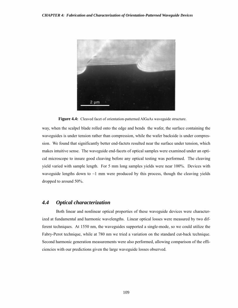
109
CHAPTER 4: Fabrication and Characterization of Orientation-Patterned Waveguide Devices
way, when the scalpel blade rolled onto the edge and bends the wafer, the surface containing the
waveguides is under tension rather than compression, while the wafer backside is under compres-
sion. We found that significantly better end-factets resulted near the surface under tension, which
makes intuitive sense. The waveguide end-facets of optical samples were examined under an opti-
cal microscope to insure good cleaving before any optical testing was performed. The cleaving
yield varied with sample length. For 5 mm long samples yields were near 100%. Devices with
waveguide lengths down to ~1 mm were produced by this process, though the cleaving yields
dropped to around 50%.
4.4 Optical characterization
Both linear and nonlinear optical properties of these waveguide devices were character-
ized at fundamental and harmonic wavelengths. Linear optical losses were measured by two dif-
ferent techniques. At 1550 nm, the waveguides supported a single-mode, so we could utilize the
Fabry-Perot technique, while at 780 nm we tried a variation on the standard cut-back technique.
Second harmonic generation measurements were also performed, allowing comparison of the effi-
ciencies with our predictions given the large waveguide losses observed.
Figure 4.4: Cleaved facet of orientation-patterned AlGaAs waveguide structure.
2 µm

CHAPTER 4: Fabrication and Characterization of Orientation-Patterned Waveguide Devices
110
4.4.1 Optical attenuation
A single-mode waveguide with input and output facets acts as a Fabry-Perot cavity and
will exhibit interference fringes similar to an etalon in the transmitted beam when the input wave-
length is varied [54]. Defining a fringe contrast K in terms of the maxima and minima of the fringe
pattern,
(4.8)
we can express K as
, (4.9)
where
. (4.10)
The waveguide losses can then be expressed as
(4.11)
where is the attenuation of the waveguide, L is the sample length, and R is the modal reflectivity
at the facet. It is optimal to extract the reflectivity by measuring devices with varying waveguide
lengths and fitting a line to the attenuation vs. length data; however, our limted sample number and
the large variability between adjacent waveguides made this technique ineffective. For a weakly
confining waveguide, the endfacet reflectivity can be approximated as
(4.12)
where is the modal effective index. If we assume this value for the reflectivity while the
actual facet reflectivity is lower due to facet imperfections or other factors, equation 4.11 indicates
that we will determine an upper bound on the propagation losses. To estimate the reflectivity, we
used the effective index calculated by the FDE solver described in Section 4.2.2 in equation 4.12.
Radiation from a 1.55 µm tunable external cavity diode laser was amplified in a erbium-
doped fiber amplifier and coupled into the waveguide using a microscope objective. A similar
microscope objective was used to image the mode from the output facet onto a Ge photodiode.
Results for a simple GaAs/Al0.1Ga0.9As waveguide of 4 mm length having a 1-µm-thick core but
no top cladding are presented in Figure 4.5. This sample had no orientation patterning or MBE
regrowth and was intended to determine what loss values we could achieve using simple MBE
KImax Imin–Imax Imin+------------------------=
K2R
1 R2
+---------------=
R R αL–( )exp=
α 4.34L
---------- R ) R( )ln–( )ln( )=
α
Rneff 1–neff 1+-----------------
2
=
neff

111
CHAPTER 4: Fabrication and Characterization of Orientation-Patterned Waveguide Devices
growth and wet chemical etching. A pattern with waveguide widths of 3 µm, 4 µm, 6 µm and
8 µm was repeated across the surface of the sample; the attenuation results from two full patterns
are shown in figure 4.5. The lowest-loss guides cluster in the neighborhood of 3-4 dB/cm and
appear across the whole sample. The large variation in attenuation losses between individual
waveguides likely results from discrete defects along the waveguides such as MBE oval defects or
lithography imperfections. Additionally, we were unable to observe light through several of the
waveguides, perhaps due to large lithography defects. The residual loss mechanism in these
guides was not determined, but is likely to be scattering from residual sidewall roughness due to
lithography and etching. In these plain MBE-grown waveguides, we achieved losses comparable
to those observed by Yoo, et al. in waveguides without orientation-patterning [55]. The fabrica-
tion processes are thus capable of achieving reasonable waveguide losses in the absence of orien-
tation-patterning.
Applying this same Fabry-Perot technique to the orientation-patterned GaAs devices, we mea-
sured fringe contrasts between 0.087 and 0.124 for 1.8 mm long waveguides containing varying
length orientation gratings (from 0.2 mm to 1.6 mm). These fringe contrasts translate into losses
of between 35 dB/cm and 60 dB/cm for that sample length. Many of the waveguides on this sam-
ple were not observed to transmit any radiation. We observe that the attenuation was not corre-
lated with the fraction of the waveguide contaning orientation patterning, or at least the
waveguide-to-waveguide variation is too large to allow clear comparison between samples of
Figure 4.5: Attenuation losses across sample for waveguides of varying ridge width.
0
5
1 0
1 5
2 0
loss
(dB
/cm
)
8 µm 8 µm6 µm 6 µm4 µm 4 µm3 µm 3 µm
waveguide location
1 mm
waveguide width:
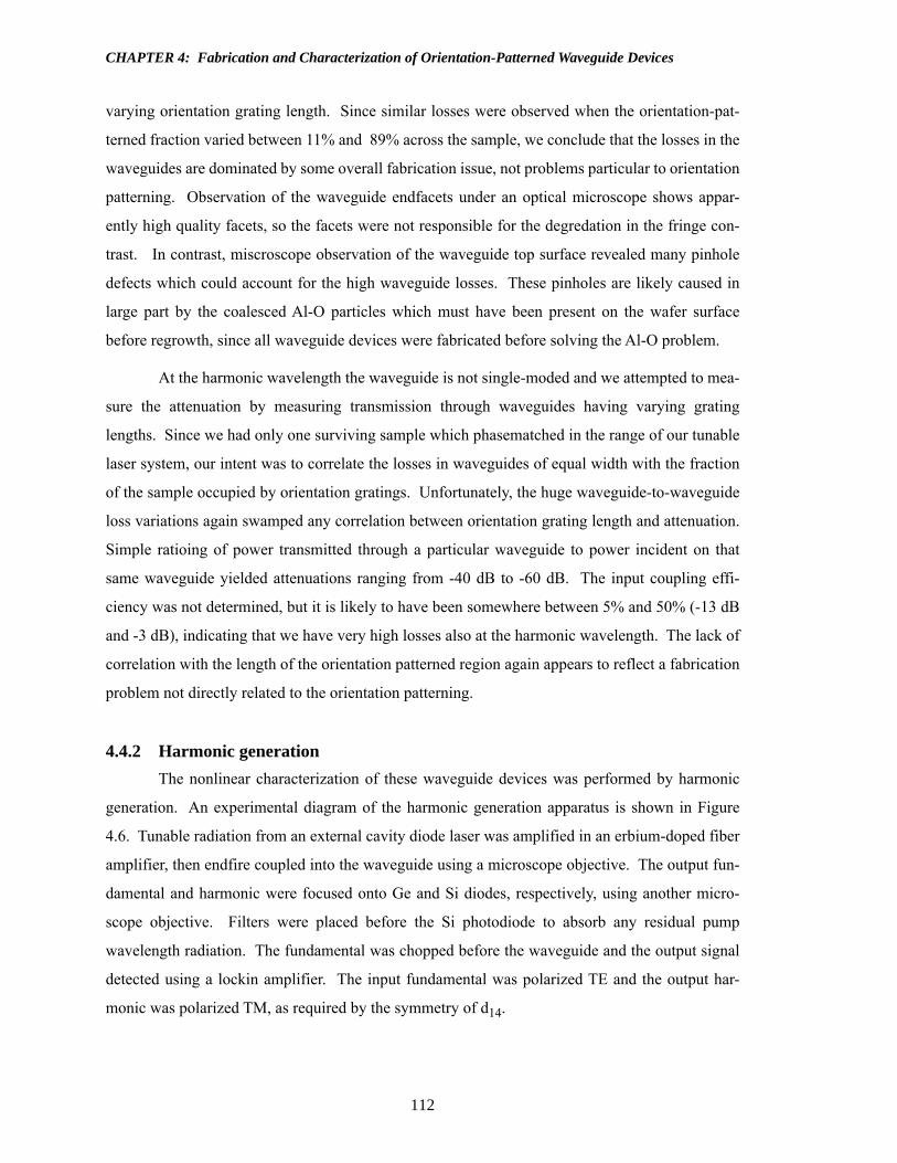
CHAPTER 4: Fabrication and Characterization of Orientation-Patterned Waveguide Devices
112
varying orientation grating length. Since similar losses were observed when the orientation-pat-
terned fraction varied between 11% and 89% across the sample, we conclude that the losses in the
waveguides are dominated by some overall fabrication issue, not problems particular to orientation
patterning. Observation of the waveguide endfacets under an optical microscope shows appar-
ently high quality facets, so the facets were not responsible for the degredation in the fringe con-
trast. In contrast, miscroscope observation of the waveguide top surface revealed many pinhole
defects which could account for the high waveguide losses. These pinholes are likely caused in
large part by the coalesced Al-O particles which must have been present on the wafer surface
before regrowth, since all waveguide devices were fabricated before solving the Al-O problem.
At the harmonic wavelength the waveguide is not single-moded and we attempted to mea-
sure the attenuation by measuring transmission through waveguides having varying grating
lengths. Since we had only one surviving sample which phasematched in the range of our tunable
laser system, our intent was to correlate the losses in waveguides of equal width with the fraction
of the sample occupied by orientation gratings. Unfortunately, the huge waveguide-to-waveguide
loss variations again swamped any correlation between orientation grating length and attenuation.
Simple ratioing of power transmitted through a particular waveguide to power incident on that
same waveguide yielded attenuations ranging from -40 dB to -60 dB. The input coupling effi-
ciency was not determined, but it is likely to have been somewhere between 5% and 50% (-13 dB
and -3 dB), indicating that we have very high losses also at the harmonic wavelength. The lack of
correlation with the length of the orientation patterned region again appears to reflect a fabrication
problem not directly related to the orientation patterning.
4.4.2 Harmonic generation
The nonlinear characterization of these waveguide devices was performed by harmonic
generation. An experimental diagram of the harmonic generation apparatus is shown in Figure
4.6. Tunable radiation from an external cavity diode laser was amplified in an erbium-doped fiber
amplifier, then endfire coupled into the waveguide using a microscope objective. The output fun-
damental and harmonic were focused onto Ge and Si diodes, respectively, using another micro-
scope objective. Filters were placed before the Si photodiode to absorb any residual pump
wavelength radiation. The fundamental was chopped before the waveguide and the output signal
detected using a lockin amplifier. The input fundamental was polarized TE and the output har-
monic was polarized TM, as required by the symmetry of d14.

113
CHAPTER 4: Fabrication and Characterization of Orientation-Patterned Waveguide Devices
The data in Figure 4.7 show the measured harmonic outout power as a function of the fun-
damental wavelength for the best device and the theoretical tuning behavior. The FWHM tuning
bandwidth agrees with the predicted 1.7 nm for this waveguide with a 0.84 mm long orientation-
patterned grating, since the device is sufficiently short to prevent the high attenuation from broad-
ening significantly the phasematching bandwidth. The effective area for this 5-µm-wide device
was calculated to be 7.2 µm2 using the FDE model described in Se ction 4.2.2. We scale d14 using
Miller’s rule to 76 pm/V for Al0.5Ga0.5As and doubling 1.55 µm. This value is consistent with the
measurements of Ohashi, et al. [56]. From equation 2.36 we predict a lossless theoretical normal-
ized internal efficiency of 13 W-1cm-2. For the 0.84 mm long orientation-patterned-grating sec-
tion present on this waveguide we tested, this corresponds to a conversion efficiency of 9.2 %/W.
We can add corrections as discussed in Section 2.1.5 for the case of significant attenuation at both
the fundamental and harmonic wavelengths. Assuming a 40 dB/cm attenuation affecting the fun-
damental and harmonic wavelengths uniformly along the length of the waveguide, we obtain a
reduced theoretical internal efficiency of 2.1 %/W. This agrees to within a factor of 2 with the
peak efficiency in Figure 4.7. Of course, the actual effect of the high attenutation is difficult to
determine, since the attenuation will be distributed unevenly along the waveguide due to discrete
defects such as pinholes. The shoulder on the tuning curve at shorter wavelength occurs because
we were operating near the shoulder of the EDFA gain peak. As the single pass gain decreases, the
amplified spontaneous emission near the EDFA gain peak (which is closer to the tuning curve
peak) increases relative to the signal at the seed wavelength set by the ECDL, so that the power
normalization becomes less accurate.
Figure 4.6: Diagram of waveguide harmonic generation experiment.
1.5 µm tunable ECDL
1.55 µmHR
1.55 µm EDFA Siphotodiode
waveguide
Gephotodiode
CHAPTER 4: Fabrication and Characterization of Orientation-Patterned Waveguide Devices
114
4.5 Discussion
With an internal conversion efficiency of 1 %/W this device is clearly not yet suitable for
applications such as WDM conversion or DFG of mid-IR radiation. The usual route of increasing
device length to improve efficiency is not possible here, as we are already into a region of signifi-
cant saturation with length due to the high losses. The very high waveguide losses are clearly dis-
appointing and significant reductions in waveguide loss will be required before orientation-
patterned waveguide devices will be practical. The most favorable strategy to improving this
device is to improve the quality of the regrown waveguiding layers as outlined in the latter part of
Chapter 3. The major candidates for the large waveguide losses observed include incomplete Al-
O removal and growth inhomogeneities of various kinds.
All waveguide devices were fabricated before we had solved the problems with Al-O con-
tamination. Since the fabrication process for all the waveguide samples involved removing
AlGaAs etch-stop layers above and below the Ge using citric acid/hydrogen peroxide, the tem-
plates presumably had Al-contamination exposed all over the top surface. The exact behavior of
the Al-O under vacuum drying in the MBE is unclear, but the samples vacuum-dried upon intro-
Figure 4.7: Harmonic generation efficiency as a function of fundamental wavelengthfor orientation-patterned AlGaAs waveguide.
0
0.2
0 .4
0 .6
0 .8
1
1 .2
1 5 2 4 1 5 2 6 1 5 2 8 1 5 3 0 1 5 3 2 1 5 3 4 1 5 3 6
SH
G e
ffic
ien
cy (
%/W
)
fundamental wavelength (nm)
FWHM = 1.7 nm
115
CHAPTER 4: Fabrication and Characterization of Orientation-Patterned Waveguide Devices
duction into the XPS system exhibited the same particle coalesence formation as was observed in
air. Whether the Al-O was distributed across the surface or concentrated into particles, MBE
regrowth would be affected. The regrown waveguide samples exhibited an uneven and streaky
haziness even to the naked eye after regrowth. Under microsopic examination a high density of
pits and depressions were observed in clear regions across the GaAs surface, presumably corre-
lated with the Al-O particle density before regrowth. Since the entire surface was covered with an
etch-stop before the final HCl-H2O dip, we would expect the surface particle density to be on
average roughly constant. This uniform roughness is a likely origin of the very high waveguide
losses observed in all waveguides across the sample, both orientation-patterned and single-orienta-
tion. With improvements in processing to eliminate this AlOx contamination, we expect that the
next generation of waveguides will have significantly lower waveguide losses.
Beyond those general issues of the material quality, the presence of various longitudinal
corrugations along the waveguide will affect the waveguide losses, though those effects were
masked in these samples by the presence of additional fabrication-related losses. However,
assuming improved regrowth quality, at some point the corrugations will dominate the waveguide
losses. From the micrograph in Figure 4.3 we can see that the clearly visible corrugation of the
core/cladding boundaries is less like a pure step-function and more like grooves which develop at
the boundaries. Whether this effect is due primarily to particle nucleation on the template stripe
edges, roughness at the template stripe boundaries, or inherently faceted growth at APBs under
these growth conditions is not yet clear. Undoubtedly these corrugations can be reduced and any
reductions in corrugation amplitude should result in lower losses once the corrugations become the
dominant loss source. Another approach to dealing with corrugation is to utilize waveguide
designs which are less sensitive to corrugations of particular spatial frequencies, since the major
contributions will exist at well-defined spatial frequencies which are various harmonics of the
domain period.
Comparing our waveguide loss results to previous work, we can see the ultimate results of
Yoo, et al. [29] are much better than ours at 1.55 um, where they measured 5 dB/cm in comparison
to our ~40 dB/cm. At 780 nm, the devices are more similar with the Bellcore results having
25 dB/cm, while we see > 40 dB/cm. Yoo, et al. attributed waveguide losses to corrugation. Their
first generation devices had losses comparable to or greater than the initial results demonstrated
here (60dB/cm at the harmonic wavelength) and those losses dropped by orders of magnitude with
improved regrowth quality. We anticipate similar improvements here with by solving the issues

CHAPTER 4: Fabrication and Characterization of Orientation-Patterned Waveguide Devices
116
complicating regrowth. Such improvements are necessary, as useful nonlinear optical waveguide
devices will require losses down into the few dB/cm range at all wavelengths of interest.
4.6 Conclusion
We have designed AlGaAs waveguides for WDM frequency conversion, fabricated them
using orientation templates and MBE regrowth, and characterized their linear and nonlinear opti-
cal properties. We find high waveguide losses of ≥ 40 dB/cm at both pump and signal wave-
lengths of 1.55 µm and 775 nm. These losses severely limit the device efficiencies to around
1 %/W by limiting the practical waveguide device length. The origins of these losses have been
examined and methods of reducing them suggested. Future research will need to focus on reduc-
tion of the waveguide losses to the point that the devices are useful for the applications envisioned.

117
CHAPTER 4: Fabrication and Characterization of Orientation-Patterned Waveguide Devices
References
1. L.A. Eyres, C.B. Ebert, P.J. Tourreau, J.S. Harris, and M.M. Fejer, "Demonstration of second
harmonic generation in all-epitaxially-grown orientation-patterned AlGaAs waveguides,"
Advanced Solid-State Lasers, Topics in Optics and Photonics Vol. 26, M.M. Fejer, H. Injeyan,
and U. Keller, eds. (Optical Society of America, Washington, DC, 1999) pp. 689-693.
2. M.L. Bortz and M.M. Fejer, "Annealed proton-exchanged LiNbO3 waveguides," Opt. Lett.
16, 1844-1846 (1991).
3. M.L. Bortz, "Quasi-phasematched optical frequency conversion in lithium niobate
waveguides," Ph. D. dissertation (Stanford University, Stanford, CA, 1994).
4. M.H. Chou, J. Hauden, M.A. Arbore, and M.M. Fejer, "1.5-µm-band wavelength conversion
based on difference-frequency generation in LiNbO3 waveguides," Opt. Lett. 23, 1004-1006
(1998).
5. M.H. Chou, I. Brener, M.M. Fejer, E.E. Chaban, and S.B. Christman, "1.5-µm-band wave-
length conversion based on cascaded second-order nonlinear susceptibility in LiNbO3," IEEE
Photonics Technol. Lett. 11, (1999).
6. K. Gallo and G. Assanto, "Analysis of lithium niobate all-optical wavelength shifters for the
third spectral window," J. Opt. Soc Am. B 16, 741-753 (1999).
7. M.H. Chou, I. Brener, G. Lenz, R. Scotti, E.E. Chaban, J. Shmulovich, D. Philen, S. Kosinski,
K.R. Parameswaran, and M.M. Fejer, "Efficient wide-band and tunable midspan spectral
inverter using cascaded nonlinearities in LiNbO3 waveguides," IEEE Photonics Technol. Lett.
12, 82-84 (2000).
8. R. Schiek, L. Friedrich, H. Fang, G.I. Stegeman, K.R. Parameswaran, M.H. Chou, and M.M.
Fejer, "Nonlinear directional coupler in periodically poled lithium niobate," Opt. Lett. 24,
1617-1619 (1999).
9. K.R. Parameswaran, M. Fujimura, M.H. Chou, and M.M. Fejer, "Low-power all-optical gate
based on sum frequency mixing in APE waveguides in PPLN," IEEE Photonics Technol. Lett.
12, 654-656 (2000).
10. S. Kawanishi, M.H. Chou, K. Fujiura, M.M. Fejer, and T. Morioka, "All-optical modulation
and time-division-multiplexing of 100 Gbit/s signal using quasi-phase matched mixing in
LiNbO3 waveguides," Electron. Lett. 36, 1568-1569 (2000).
11. I. Brener, M.H. Chou, E.E. Chaban, K.R. Parameswaran, M.M. Fejer, S. Kosinski, and D.L.
Pruitt, "Polarization-insensitive wavelength converter based on cascaded nonlinearities in
LiNbO3 waveguides," Electron. Lett. 36, 66-67 (2000).

CHAPTER 4: Fabrication and Characterization of Orientation-Patterned Waveguide Devices
118
12. S.J.B. Yoo, C. Caneau, R. Bhat, M.A. Koza, A. Rajhel, and N. Antoniades, "Wavelength con-
version by difference frequency generation in AlGaAs waveguides with periodic domain
inversion achieved by wafer bonding," Appl. Phys. Lett. 68, 2609-2611 (1996).
13. K.P. Petrov, A.P. Roth, T.L. Patterson, T.P.S. Thoms, L. Huang, A.T. Ryan, and D.J. Bamford,
"Efficient difference-frequency mixing of diode lasers in lithium niobate channel
waveguides," Appl. Phys. B 70, 777-782 (2000).
14. K.P. Petrov, A.T. Ryan, T.L. Patterson, L. Huang, S.J. Field, and D.J. Bamford, "Spectro-
scopic detection of methane by use of guided-wave diode-pumped difference-frequency gen-
eration," Opt. Lett. 23, 1052-1054 (1998).
15. M.H. Chou, M.A. Arbore, and M.M. Fejer, "Adiabatically tapered periodic segmentation of
channel waveguides for mode-size transformation and fundamental mode excitation," Opt.
Lett. 21, 794-796 (1996).
16. J.T. Boyd, "Theory of parametric oscillation phase matched in GaAs thin-film waveguides,"
IEEE J. Quantum Electron. 8, 788-796 (1972).
17. J.P. Van der Ziel and M. Illegems, "Second harmonic generation in a thin AlAs-GaAs multi-
layer structure with wave propagation in the plane of the layers," Appl. Phys. Lett. 29, 200-
202 (1976).
18. A. Fiore, S. Janz, L. Delobel, P. Van der Meer, P. Bravetti, V. Berger, E. Rosencher, and J.
Nagle, "Second-harmonic generation at lambda = 1.6 µm in AlGaAs/Al2O3 waveguides using
birefringence phase matching," Appl. Phys. Lett. 72, 2942-2944 (1998).
19. A. Fiore, V. Berger, E. Rosencher, P. Bravetti, N. Laurent, and J. Nagle, "Phase-matched mid-
infrared difference frequency generation in GaAs-based waveguides," Appl. Phys. Lett. 71,
3622-3624 (1997).
20. P. Bravetti, A. Fiore, V. Berger, E. Rosencher, J. Nagle, and O. Gauthier-Lafaye, "5.2-5.6-µm
source tunable by frequency conversion in a GaAs-based waveguide," Opt. Lett. 23, 331
(1998).
21. M.W. Street, N.D. Whitbread, D.C. Hitchings, J.M. Arnold, J.H. Marsh, J.S. Aitchison, G.T.
Kennedy, and W. Sibbett, "Quantum-well intermixing for the control of second-order nonlin-
ear effects in AlGaAs multiple-quantum-well waveguides," Opt. Lett. 22, 1600-1602 (1997).
22. M.W. Street, N.D. Whitbread, C.J. Hamilton, B. Vogele, C.R. Stanley, D.C. Hutchings, J.H.
Marsh, J.S. Aitchison, G.T. Kennedy, and W. Sibbett, "Modification of the second-order opti-
cal nonlinearities in AlGaAs asymmetric multiple quantum well waveguides by quantum well
intermixing," Appl. Phys. Lett. 70, 2804-2806 (1997).
119
CHAPTER 4: Fabrication and Characterization of Orientation-Patterned Waveguide Devices
23. S. Janz, M. Buchanan, P. Van der Meer, Z.R. Wasilewski, D.X. Xu, P. Piva, I.V. Matchell,
U.G. Akano, and A. Fiore, "Patterning the second-order optical nonlinearity of asymmetric
quantum wells by ion implantation enhanced intermixing," Appl. Phys. Lett. 72, 3097-3099
(1998).
24. J.P. Bouchard, M. Tetu, S. Janz, D.X. Xu, Z.R. Wasilewski, P. Piva, U.G. Akano, and I.V.
Mitchell, "Quasi-phase matched second-harmonic generation in an AlxGa1-xAs asymmetric
quantum-well waveguide using ion-implantation-enhanced intermixing," Appl. Phys. Lett.
77, 4247-4249 (2000).
25. R. Lodenkamper, M.L. Bortz, M.M. Fejer, K. Bacher, and J.S. Harris, "Surface-emitting sec-
ond-harmonic generation in a semiconductor vertical resonator," Opt. Lett. 18, 1798-1800
(1993).
26. A. Fiore, Y. Beaulieu, S. Janz, J.P. McCaffrey, Z.R. Wasilewski, and D.X. Xu, "Quasiphase
matched surface emitting second harmonic generation in periodically reversed asymmetric
GaAs/AlGaAs quantum well waveguide," Appl. Phys. Lett. 70, 2655-2657 (1997).
27. S. Janz, Y. Beaulieu, A. Fiore, P. Bravetti, V. Berger, E. Rosencher, and J. Nagle, "Surface-
emitted second-harmonic generation from a quasi-phasematched waveguide in an AlxGa1-
xAs/Al2O3 microcavity," Optics Express 2, (1998).
28. S.J.B. Yoo, R. Bhat, C. Caneau, and M.A. Koza, "Quasi-phase-matched second-harmonic
generation in AlGaAs waveguides with periodic domain inversion achieved by wafer-bond-
ing," Appl. Phys. Lett. 66, 3410-3412 (1995).
29. S.J.B. Yoo, M.A. Koza, R. Bhat, and C. Caneau, "Bidirectionally pumped difference-fre-
quency generation in AlGaAs waveguides: polarization-independent, multichannel wav-
length conversion with input signal filtering capabilities," Conference on Lasers and Electro-
Optics, OSA Trends in Optics and Photonics Vol. 6 (Optical Society America, Washington,
DC, 1998) pp. 107-108.
30. J. Stultius and Z. Streifer, "Silicon nitride films on silicon for optical waveguides," Appl. Opt.
16, 3218-3222 (1977).
31. J. Buus, "The effective index method and its application to semiconductor lasers," IEEE J.
Quantum Electron. QE-18, 1083-1089 (1982).
32. M.W. Austin, "Theoretical and experimental investigation of GaAs/GaAlAs and n/n+ GaAs
Rib waveguides," J. Lightwave Tech. 2, 688-693 (1984).
33. M.S. Stern, "Semivectorial polarised finite difference method for optical waveguides with
arbitrary index profiles," IEE Proc. J 135, 56-63 (1988).
34. M.S. Stern, "Rayleigh quotient solution of semivectorial field problems for optical
waveguides with arbitrary index profiles," IEE Proc. J 138, 185-190 (1991).

CHAPTER 4: Fabrication and Characterization of Orientation-Patterned Waveguide Devices
120
35. H.P. Zappe, Introduction to Semiconductor Integrated Optics (Artech House, Boston, 1995).
36. R.G. Hunsperger, Integrated optics: Theory and Technology (Springer-Verlag, New York,
1995).
37. V.I. Vdovin, M.G. Mil'vidskii, and T.G. Yugova, "Antiphase boundaries in GaAs layers on Si
and Ge," J. Cryst. Growth 132, 477-482 (1993).
38. Y. Li and L.J. Giling, "A closer study on the self-annihilation of antiphase boundaries in
GaAs epilayers," J. Cryst. Growth 163, 203-211 (1996).
39. T. Yamada and Y. Horikoshi, "Comparison of GaAs facet formation on patterned substrate
during molecular beam epitaxy and migration enhanced epitaxy," Jpn. J. Appl. Phys. 33,
L1027-L1030 (1994).
40. E. Kapon and R. Bhat, "Low-loss single-mode GaAs/AlGaAs optical waveguides grown by
organometallic vapor phase epitaxy," Appl. Phys. Lett. 50, 1628-1630 (1987).
41. M. Seto, R.J. Deri, A. Yi-Yan, E. Colas, W.J. Tomlinson, R. Bhat, and A. Shahar, "Fabrication
of submillimeter-radius optical waveguide bends with anisotropic and isotropic wet chemical
etchants," J. Lightwave Tech. 8, 264-270 (1990).
42. M.K. Hibbs-Brenner and C.T. Sullivan, "Low-loss AlGaAs optical rectangular waveguides at
830 nm," Appl. Phys. Lett. 56, 1529-1531 (1990).
43. R.J. Deri, E. Kapon, J.P. Harbison, M. Seto, C.P. Yun, and L.T. Florez, "Low-loss
GaAs/AlGaAs waveguide phase modulator using a W-shaped index profile," Appl. Phys. Lett.
53, 1803-1805 (1988).
44. R.J. Deri, E. Kapon, R. Bhat, M. Seto, and K. Kash, "Low-loss multiple quantum well
GaInAs/InP optical waveguides," Appl. Phys. Lett. 54, 1737-1739 (1989).
45. P. Buchmann, H. Kaufmann, H. Melchior, and G. Guekos, "Reactive ion etched GaAs optical
waveguide modulators with low loss and high speed," Electron. Lett. 20, 295-297 (1984).
46. P.W. McIlroy, P.M. Rodgers, J.S. Singh, P.C. Spurdens, and I.D. Henning, "Low-loss single-
mode InP/InGaAsP waveguides grown by MOVPE," Electron. Lett. 23, 701-703 (1987).
47. R.J. Deri, E. Kapon, and L.M. Schiavone, "Scattering in low-loss GaAs/AlGaAs rib
waveguides," Appl. Phys. Lett. 51, 789-790 (1987).
48. H. Inoue, K. Hiruma, K. Ishida, T. Asai, and H. Matsumura, "Low loss GaAs optical
waveguides," J. Lightwave Tech. LT-3, 1270-1275 (1985).
49. D.W. Shaw, "Localized GaAs etching with acidic hydrogen peroxide solutions," J. Electro-
chem. Soc. 128, 874-880 (1981).
50. M. Tong, D.G. Ballegeer, A. Ketterson, E.J. Roan, K.Y. Cheng, and I. Adesida, "A compara-
tive study of wet and dry selective etching processes for GaAs/AlGaAs/InGaAs Pseudomor-
phic MODFETs," Jour. Electron. Mater. 21, 9-15 (1992).

121
CHAPTER 4: Fabrication and Characterization of Orientation-Patterned Waveguide Devices
51. H.K. Kuiken, J.J. Kelly, and P.H.L. Notten, "Etching profiles at resist edges I: Mathematical
models for diffusion-controlled cases," J. Electrochem. Soc. 133, 1217-1226 (1986).
52. P.H.L. Notten, J.J. Kelly, and H.K. Kuiken, "Etching profiles at resist edges II: Experimental
confirmation of models using GaAs," J. Electrochem. Soc. 133, 1226-1232 (1986).
53. S. Adachi and K. Oe, "Chemical etching characteristics of (001) GaAs," J. Electrochem. Soc.
130, 2427-2435 (1983).
54. R. Regener and W. Sohler, "Loss in low-finesse Ti:LiNbO3 optical waveguide resonators,"
Appl. Phys. B 36, 143-147 (1985).
55. S.J.B. Yoo, personal communication to L.A. Eyres (1998).
56. M. Ohashi, T. Kondo, R. Ito, S. Fukatsu, Y. Shiraki, K. Kumata, and S.S. Kano, "Determina-
tion of quadratic nonlinear optical coefficient of AlxGa1-xAs system by the method of
reflected second harmonics," J. Appl. Phys. 74, 596-601 (1993).

CHAPTER 4: Fabrication and Characterization of Orientation-Patterned Waveguide Devices
122

123
CHAPTER 5: Growth and Characterization of Thick Orientation-Patterned GaAs
5.1 Introduction
Given the excellent vertical domain propagation observed in thin film orientation-pat-
terned semiconductor growth, a natural question arises: can such domain quality be preserved
through thicker layers (> 0.5 mm) suitable for bulk-focused frequency conversion? There are sig-
nificant advantages to having larger apertures for some frequency conversion applications, partic-
ularly those requiring high power-handling capability. Also, since the radiation is not confined by
a dielectric structure, the attenuation losses and device performance are less dependent on compli-
cated issues of expitaxial growth morphology, making possible faster device development.
This chapter will review our investigations into the growth and characterization of thick
orientation-patterned GaAs films. It opens with a discussion of the growth techniques suitable for
producing such thick films, focusing particularly the HVPE process. Next, we investigate issues
of orientation-patterned film quality and characteristic defects in thick GaAs films, demonstrating
that thick orientation-patterned GaAs films with high domain quality are achievable. After dis-
cussing the linear optical properties of these films, the chapter will close with the results of har-
monic generation experiments that confirm the utility of these films for frequency conversion
applications. Many of the results have been published in [1, 2].
5.2 Thick GaAs growth processes
Several techniques are capable of growing significantly thicker GaAs apertures than the
~10 um available in MBE, including MOCVD [3], chloride vapor phase epitaxy (Cl-VPE) [4-6],
hydride vapor phase epitaxy (HVPE) [7, 8] and close-spaced vapor transport (CSVT)[9, 10]. The
primary issues in extension to much thicker films are the much larger source volumes necessary
and the elimination of UHV vacuum requirements and associated overhead on source reloading.
We investigated thick orientation-patterned GaAs growth by two of these techniques, Cl-VPE and
HVPE. In both cases, the thick growth experiments were performed in collaboration with groups
already operating the requisite reactors. To date, only HPVE has demonstrated films with high
quality domains, for reasons which are explored in more detail below.
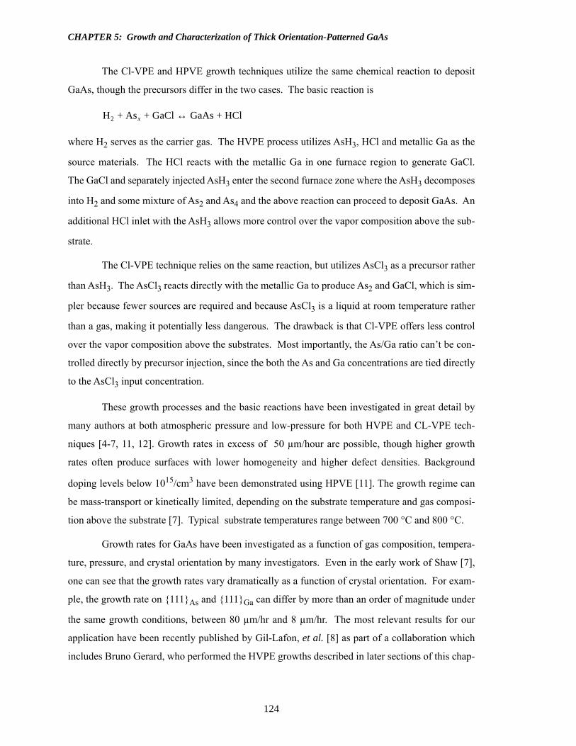
CHAPTER 5: Growth and Characterization of Thick Orientation-Patterned GaAs
124
The Cl-VPE and HPVE growth techniques utilize the same chemical reaction to deposit
GaAs, though the precursors differ in the two cases. The basic reaction is
where H2 serves as the carrier gas. The HVPE process utilizes AsH3, HCl and metallic Ga as the
source materials. The HCl reacts with the metallic Ga in one furnace region to generate GaCl.
The GaCl and separately injected AsH3 enter the second furnace zone where the AsH3 decomposes
into H2 and some mixture of As2 and As4 and the above reaction can proceed to deposit GaAs. An
additional HCl inlet with the AsH3 allows more control over the vapor composition above the sub-
strate.
The Cl-VPE technique relies on the same reaction, but utilizes AsCl3 as a precursor rather
than AsH3. The AsCl3 reacts directly with the metallic Ga to produce As2 and GaCl, which is sim-
pler because fewer sources are required and because AsCl3 is a liquid at room temperature rather
than a gas, making it potentially less dangerous. The drawback is that Cl-VPE offers less control
over the vapor composition above the substrates. Most importantly, the As/Ga ratio can’t be con-
trolled directly by precursor injection, since the both the As and Ga concentrations are tied directly
to the AsCl3 input concentration.
These growth processes and the basic reactions have been investigated in great detail by
many authors at both atmospheric pressure and low-pressure for both HVPE and CL-VPE tech-
niques [4-7, 11, 12]. Growth rates in excess of 50 µm/hour are possible, though higher growth
rates often produce surfaces with lower homogeneity and higher defect densities. Background
doping levels below 1015/cm3 have been demonstrated using HPVE [11]. The growth regime can
be mass-transport or kinetically limited, depending on the substrate temperature and gas composi-
tion above the substrate [7]. Typical substrate temperatures range between 700 °C and 800 °C.
Growth rates for GaAs have been investigated as a function of gas composition, tempera-
ture, pressure, and crystal orientation by many investigators. Even in the early work of Shaw [7],
one can see that the growth rates vary dramatically as a function of crystal orientation. For exam-
ple, the growth rate on {111}As and {111}Ga can differ by more than an order of magnitude under
the same growth conditions, between 80 µm/hr and 8 µm/hr. The most relevant results for our
application have been recently published by Gil-Lafon, et al. [8] as part of a collaboration which
includes Bruno Gerard, who performed the HVPE growths described in later sections of this chap-
H2 + Asx + GaCl GaAs + HCl↔

125
CHAPTER 5: Growth and Characterization of Thick Orientation-Patterned GaAs
ter. They investigated the relative growth rates on varying GaAs facets as a function of HVPE
growth conditions and resulting morphology of growth on patterned surfaces. With the control
over vapor composition afforded by HVPE, they could parametrize the growth rates as a function
of substrate temperature, vapor supersaturation, and III/V ratio. They find that for a III/V ratio of
4.5, low supersaturation, and a growth temperature of 730 °C, the growth rate hierarchy is {111}Ga
>> {001} > {110} ≥ {110}As. When the III/V ratio is increased or widely decreased, the growth
rate of {111}As drops significantly below that of {110}. Under high supersaturation conditions,
the growth rate of the {111}Ga drops below that of {001}. When growth is performed on masked
regions or etched stripes, the facets exhibited after HPVE growth naturally correspond to those
having the lowest growth rates under those particular growth conditions. Knowledge of these rel-
ative growth rates will allow interpretation of the surface morphologies observed on orientation-
patterned GaAs films.
5.2.1 Growth by CL-VPE
Our first attempts at thick GaAs growth were performed by CL-VPE in collaboration with
researchers at the Ioffe Institute in St. Petersburg, Russia. Orientation templates with 5-µm MBE-
GaAs grown on top were used to seed growth of 100-µm-thick GaAs films. Typical results of this
growth experiment are shown in Figure 5.1. The antiphase boundary has been marked to make it
easily visible. The other vertical lines are artifacts of the sample cleaving. One can see that the
APB wanders in direction locally between {111} and {100}, with vertical propagation observed
only for short sections. This propagation naturally results in domains closing over in a thickness
comparable the original domain width. While the exact antiphase domain boundary cross-section
differed from boundary to boundary across the sample, all such boundaries exhibited the same
general propagation direction and domain annihilation behavior. The local changes in APB
growth direction are likely due to localized changes in growth parameters such as vapor concentra-
tion. Having only a single Cl-VPE thick GaAs growth run made it impossible to determine the
factors controlling domain behavior. In addition, because the collaborators who performed the
thick growth were unwilling disclose details about the growth process, we are unable to speculate
about whether changes in the growth parameters would make a significant difference in the APB
propagation behavior.

CHAPTER 5: Growth and Characterization of Thick Orientation-Patterned GaAs
126
5.2.2 Growth by HVPE
After the Cl-VPE processs yielded poor domain quality, our focus turned to HPVE
growth, which allows more independent control over the vapor composition above the substrate.
Templates similar to those for Cl-VPE were fabricated with 5 µm MBE GaAs on top to seed the
thick growth. For these experiments, the thickness of the GaAs layer on top of the Ge was
increased to 1000 Å in order to eliminate pinholes produced during the template-producing etch-
ing steps. The template was cleaved into samples of approximately 1 cm2 before HVPE growth in
order to allow for multiple sample runs from the limited wafer area available. Among the few
samples which had thick GaAs grown on top included 212-µm periods, 27-µm periods and several
other periods with the grating k-vectors aligned both parallel and perpendicular to the in-plane
misorientation direction.
The thick GaAs was grown at Thales (Thomson-CSF) Central Research Laboratory in
Orsay, France by Bruno Gerard. The hot-wall horizontal quartz reactor has two inlets, one for the
flow of HCl+H2 over the 7N Ga source and the other bypassing the source for AsH3, main H2 car-
rier flow and additional HCl. The total flow was about 1 standard liter/minute. The temperatures
of the Ga source and of the GaAs substrate were kept at 850°C and 750°C, respectively, and the
growth was carried out at atmospheric pressure. The vertical growth rate was about 10 µm/hr. By
Figure 5.1: Cross-section of 100-µm-thick GaAs film grown by Cl-VPE.APB is marked in black for easier identification.
100 µm Cl-VPE GaAs
orientation template
25 µm
[110 ]
[001 ]

127
CHAPTER 5: Growth and Characterization of Thick Orientation-Patterned GaAs
varying the composition of the vapor phase (III/V ratio between 3 to 10), different lateral facets of
the stripes growing on (100) or (-100) surfaces can be obtained, either of {011} or {111}types [8,
13, 14]. For the present application, only growth conditions consistent with {011}facets were uti-
lized in order to preserve the width of the anti-phase domains.
After thick GaAs growth, the samples were polished to expose the domain structure.
Stain-etching of the domains was attempted using the same potassium ferricyanide etch as was
discussed in Chapter 4, but no signs of the domain boundaries were visible in the optical or elec-
tron microscopes. Instead we employed a selective etch which attacked different GaAs crystal ori-
entations at different rates, leading to a corrugation visible by optical microscopy on the
previously polished surface. An etch of (1:1:100) NH3OH:H2O2:H2O worked well for this pur-
pose, after which the samples were characterized using an optical microscope.
Figure 5.2 shows a top view and cross-section of a 200-µm-thick GaAs film grown by
HVPE with a 27-µm domain period. In comparison to the previous results using Cl-VPE, the
domain boundaries here grow almost exclusively vertically, so that the domain duty cycle is pre-
served up through the thick GaAs. No change in duty cycle was measureable for the majority of
domains. This behavior is clearly optimal for use in quasi-phasematched frequency conversion
applications, since the desired susceptibility modulation will be preserved in the region of the opti-
cal radiation. In this case, the grating k-vector was aligned perpendicular to the surface misorien-
tation direction, so that the APBs lie approximately in {110}. This behavior is consistent with the
observations of Li, [15], who observed stable propagation of APBs in {110} for MOCVD growth
under As-rich growth conditions. All samples with domain periods from 212 µm to 27 µm with
the same grating orientation show similarly vertical boundaries. The reasons for the differences in
APB propagation between this HPVE film and the previous results using CL-VPE are not clear
given our limited knowledge of the exact growth conditions. However, the previously discussed
stability of {110} facets under the HVPE growth conditions utilized is an intuitively appealing
condition. Firm conclusions about the APB propagation dependence on growth conditions await
more extensive thick growth results, but two things are clear from our limited experiments. First,
the same basic reaction can yield GaAs films with radically different APB propagation. More
importantly, there exist HVPE conditions under which APBs propagate in stable vertical fashion
through film thicknesses useful for bulk frequency conversion.

CHAPTER 5: Growth and Characterization of Thick Orientation-Patterned GaAs
128
5.3 Characterization of thick GaAs films
In this section we examine three important aspects of thick GaAs growth which affect the
ultimate film and domain quality. We find a dependence on grating direction relative to the sur-
face misorientation, examine the surface morphology and its connection to the growth rate, and
observe two types of defects across the surface which degrade the domain quality.
5.3.1 Grating orientation and domain quality
To understand the effects of grating orientation on the domain quality, we can compare the
results presented in the last section with gratings having k-vectors aligned in the orthogonal direc-
tion, so that the grating k-vectors are parallel to the in-plane substrate misorientation direction
. Figure 5.3 illustrates two possible relative orientations of the grating k-vectors with
respect to the atomic terrace steps running down the surface. To remove any ambiguity, we take
the direction of the steps (misorientation direction) to point down the atomic staircase. Figure 5.3a
shows the case of Figure 5.2, with the step direction perpendicular to the k-vector, while Figure
Figure 5.2: Stain-etched 200-µm-thick OPGaAs film with 27-µm domain periodgrown by HVPE showing a) top view and b) polished cross section. Grating k-vector isaligned antiparallel to in-plane surface misorientation direction.
100 µm
[011]
[100]
[011]
[100]
(a)
substrate
MBE GaAs
HVPE GaAs
(b)
110[ ]

129
CHAPTER 5: Growth and Characterization of Thick Orientation-Patterned GaAs
5.3b shows the case with the step direction and k-vector parallel. Unfortunately, the limited num-
ber of samples grown precludes us from comparing precisely the same periods, but the differences
in behavior are still sufficiently clear to draw conclusions.
Figure 5.4 shows the stain-etched cross-section of a sample with misorientation direction
parallel to the grating k-vector. The domain boundaries appear to be largely propagating in {110},
but now {110} is tilted with respect to the wafer surface by the 4° misorientation. Despite the fact
that this sample has domains almost four times as wide as the domains in Figure 5.2, the domain
quality is clearly much worse. Figure 5.4 shows one of the highest quality regions observed with
this grating orientation relative to the wafer misorientation; most areas are much worse with a
more corrugated surface, more overgrown domains, and more wander in the APB boundary direc-
tions. The domain growth is clearly affected by some factor which results in wide variation in
domain cross-section, height, and profile. Note also that the domains in Figure 5.4 annihilate by
no regular mechanism, in contrast to the symmetric domain overgrowth observed in Figure 5.2.
The most probable explanation for the difference between the two grating orientations is
inhibited step flow and problematic nucleation across the APBs. The two cases are nominally
identical in crystal orientation, with only the 4° misorientation breaking the symmetry. With the k-
vector and the surface misorientation perpendicular, both domains can grow by simple step flow
across the wafer and no nucleation of new atomic layers across APB boundaries is required except
at the very end of the long domain. In contrast, for the parallel k-vector case, where step flow
growth is interrupted by antiphase domain boundaries, nucleation must occur across the APB
before step flow growth can proceed further across the next domain. This inhibited nucleation
Figure 5.3: Grating k-vector alignment relative to the surface misorientationdirection, a) antiparallel, b) parallel.
grating k-vector grating k-vector
misorientationdirection [110](down atomic
staircase)
a) b)
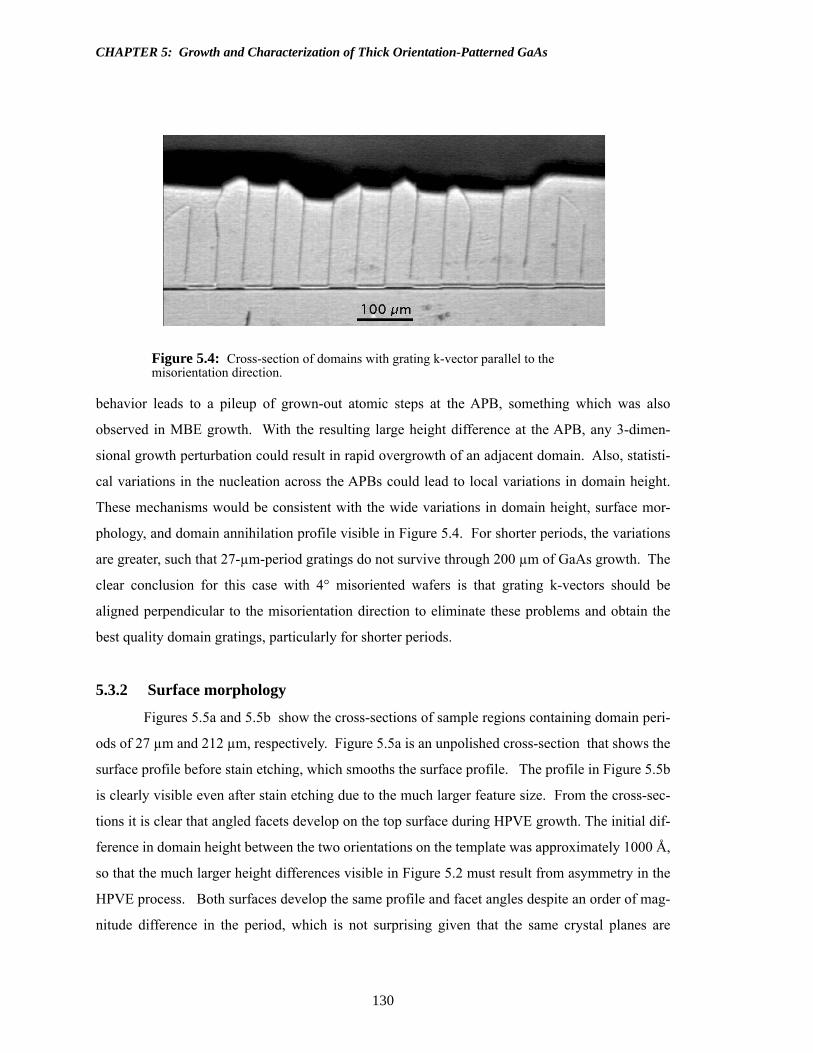
CHAPTER 5: Growth and Characterization of Thick Orientation-Patterned GaAs
130
behavior leads to a pileup of grown-out atomic steps at the APB, something which was also
observed in MBE growth. With the resulting large height difference at the APB, any 3-dimen-
sional growth perturbation could result in rapid overgrowth of an adjacent domain. Also, statisti-
cal variations in the nucleation across the APBs could lead to local variations in domain height.
These mechanisms would be consistent with the wide variations in domain height, surface mor-
phology, and domain annihilation profile visible in Figure 5.4. For shorter periods, the variations
are greater, such that 27-µm-period gratings do not survive through 200 µm of GaAs growth. The
clear conclusion for this case with 4° misoriented wafers is that grating k-vectors should be
aligned perpendicular to the misorientation direction to eliminate these problems and obtain the
best quality domain gratings, particularly for shorter periods.
5.3.2 Surface morphology
Figures 5.5a and 5.5b show the cross-sections of sample regions containing domain peri-
ods of 27 µm and 212 µm, respectively. Figure 5.5a is an unpolished cross-section that shows the
surface profile before stain etching, which smooths the surface profile. The profile in Figure 5.5b
is clearly visible even after stain etching due to the much larger feature size. From the cross-sec-
tions it is clear that angled facets develop on the top surface during HPVE growth. The initial dif-
ference in domain height between the two orientations on the template was approximately 1000 Å,
so that the much larger height differences visible in Figure 5.2 must result from asymmetry in the
HPVE process. Both surfaces develop the same profile and facet angles despite an order of mag-
nitude difference in the period, which is not surprising given that the same crystal planes are
Figure 5.4: Cross-section of domains with grating k-vector parallel to the misorientation direction.

131
CHAPTER 5: Growth and Characterization of Thick Orientation-Patterned GaAs
exposed. Comparing to previous HVPE growth experiments on stripes [8, 14], it is likely the 27-
µm-period sample exhibits the equilibrium morphology, so that the 212-µm-period sample in Fig-
ure 5.4b should develop the triangular profile of Figure 5.4a with additional HPVE growth. The
measured angle of the facets with respect to the GaAs wafer surface is approximately 35°, so that
the facets lie near {112}.
The faceting behavior observed can be understood by reference to the heirarchy of facet
growth rates observed by Gil-Lafon, et al. [8] under HVPE growth conditions consistent with pri-
marily {110} sidewalls. Consider first the growth of a uniform <110> stripe of each orientation
growing in isolation, with the surrounding surface masked. In this case, Gil-Lafon, et al. observed
that both of the isolated domains have approximately the same shape as the domains observed in
our orientation-patterned film of Figure 5.5a; one orientation has a triangular top and the other has
a flat top. For the first stripe orientation, with {111}As exposed on the corners, the important fac-
ets are the low-index {100} and {111}As. Since the {100} growth rate is much higher than the
{111}As rate, the stripe tops exhibit {111} facets and appear triangular in cross-section. For the
orthogonal stripe orientation, the important facets are {100} and the {111}Ga, which would be
exposed on the corners. With the high growth rate measured on {111}Ga, one observes that the
stripe corners grow out quickly and leave a flat {100} top, exactly like the flat top domains in Fig-
ure 2.5a. The exhibition of approximately {112} on the triangular domains in our orientation-pat-
terned films rather than {111} may result from effects of the nearby APB or adjacent domain of
opposite orientation. Either of these could could change the nucleation rate at the bottom of the
facet and therefore modify the angle from what one would expect with an isolated stripe. It is
unclear exactly how the surface morphology might affect the APD propagation, especially in the
presence of defects of the kinds discussed in the next section. The only clear conclusion is that
this equilibrium morphology is compatible with overall vertical APB propagation.
One can speculate about the overall growth rate of the orientation-patterned surface by
considering the facets exposed on the surface, as illustrated in Figure 2.6. Under these growth
conditions, triangular domains would be expected to exhibit a slow growth facet {111}As on both
sides and therefore necessarily grow slowly. The flat domains would grow vertically at the {001}
growth rate and should preserve their rectangular shape due to the presence of the slow growth
{110} exposed on the sidewalls. The two isolated domains would thus be expected to grow at sig-
nificantly different rates, yet in Figure 5.5 the equilibrium angled and horizontal facets of the two
domains meet at the APB boundaries. This indicates that the overall growth rate is somehow cou-

CHAPTER 5: Growth and Characterization of Thick Orientation-Patterned GaAs
132
pled across the APB. This overall rate must be dominated by the higher {001} growth rate on the
flat surfaces. The flat domain will grow at the rate-limited {100} growth rate, but have straight
{110} sidewalls. Thus, it will tend not to overgrow the adjacent triangular domain, bounded as it
is by the slow growth {110} which becomes the APB plane, at least in the absence of 3-D surface
perturbations. As the rectangular domain grows it might well enhance the probability of nucle-
ation of layers on the angled facet across the APB boundary. Addition of atoms to the flat domain
would increase the number of nearest neighbor bonds possible for an atom incorporating at the
APB and potentially lower the barrier to nucleation of new atomic planes on the angled facet. It
seems reasonable to assume that this nucleation rate at the base of the angled facet would be pro-
portional to the growth rate on the flat (001) surface. Growth on the angled facet could then occur
primarily by step flow growth from the APB nucleation region up towards the peak, resulting in an
angled facet whose net vertical growth rate matched that of the {001} surface. This explanation
could account for the tilt direction of the angled facet away from {111} towards {112} and for the
resulting approximately uniform growth rate across the surface.
5.3.3 Domain defects
Figure 5.7 shows the top view of the 27-µm-period domain sample exhibiting a variety of
domain defects. Almost all the interrupted domains can be associated with two kinds of defects,
individual domain interruptions and pyramidal 3-D growth defects which disrupt multiple
domains. On any given cross-section through the 27-µm-period sample, approximately 10% of
Figure 5.5: Surface morphology of 27-µm- and 212-µm-period OPGaAs films.The 27 µm period sample was cleaved; the 212 µm period sample was polished andstain-etched.
27 µm 212 µma) b)
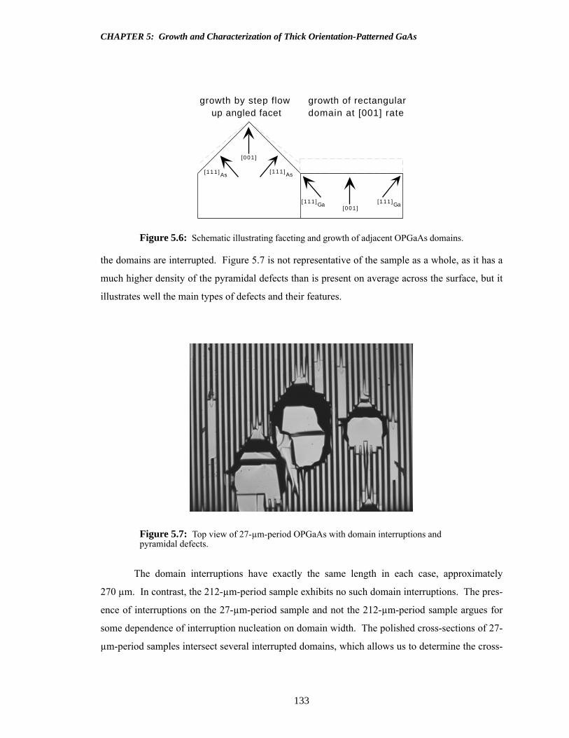
133
CHAPTER 5: Growth and Characterization of Thick Orientation-Patterned GaAs
the domains are interrupted. Figure 5.7 is not representative of the sample as a whole, as it has a
much higher density of the pyramidal defects than is present on average across the surface, but it
illustrates well the main types of defects and their features.
The domain interruptions have exactly the same length in each case, approximately
270 µm. In contrast, the 212-µm-period sample exhibits no such domain interruptions. The pres-
ence of interruptions on the 27-µm-period sample and not the 212-µm-period sample argues for
some dependence of interruption nucleation on domain width. The polished cross-sections of 27-
µm-period samples intersect several interrupted domains, which allows us to determine the cross-
Figure 5.6: Schematic illustrating faceting and growth of adjacent OPGaAs domains.
Figure 5.7: Top view of 27-µm-period OPGaAs with domain interruptions and pyramidal defects.
[ 111 ]As[111 ]As
[001 ]
[111 ]Ga[111 ]Ga[001 ]
growth of rectangulardomain at [001] rate
growth by step flow up angled facet

CHAPTER 5: Growth and Characterization of Thick Orientation-Patterned GaAs
134
sectional profiles of these defects. For each interrupted domain we can measure the height at
which the domain closes over and the remaining interrupted distance between the polished edge
and the point where the domain is again observable on the sample surface. Figure 5.8 illustrates
these quantities.
Figure 5.9 shows the interrupted domain heights at the polished cross-section as a function
of the distance from the edge of the interruption. The fact that the domain heights fall on a sharp
line indicates that each domain interruption has the same cross-sectional profile. The uniform
domain interruption length and cross-section indicate a similar origin for the interruptions, while
the profile points approximately back toward the template as the origin. The solid line fit in figure
5.9 is at approximately 32.9° with respect to the wafer surface, which when added to the 4° ± 0.5°
wafer misorientation corresponds approximately to the 35.3° expected for a boundary propagating
in the {112} plane. Note that the asymmetry in the domain interruption must result from the 4°
wafer misorientation, since otherwise the domain interruption ought to be symmetric. The dashed
line in Figure 5.8 is a guess about the profile of the opposite side of the domain interruption which
connects the re-appearance of the domain on the surface with the probable location of the defect in
the template. However, no cases were seen in the polished cross-sections with inverted domains
suddenly appearing some distance up in the film. Possible origins of the interruptions include oval
defects in the original MBE growths (either in template or regrowth), dirt/contamination from wet
processing, or lithograpy defects. All three would be consistent with the linewidth dependence we
see of the interruptions. The characteristic size of the defect may need to be sufficiently large to
interrupt the whole domain, something more probable for narrow domains than wide ones. As this
problem appears to originate at the template, improved template processing should result in a
reduction of the interruption density.
Figure 5.8: Schematic of interrupted domain quantities used to determine domain profiles.
domain height
remaining interruption
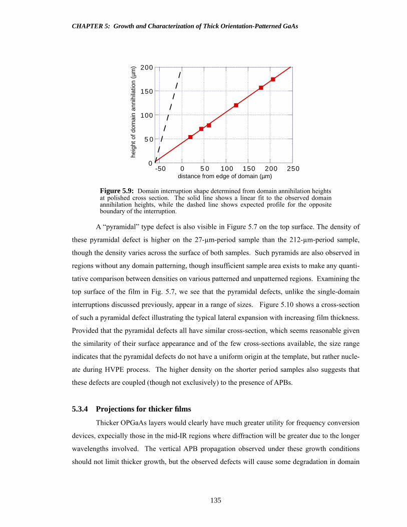
135
CHAPTER 5: Growth and Characterization of Thick Orientation-Patterned GaAs
A “pyramidal” type defect is also visible in Figure 5.7 on the top surface. The density of
these pyramidal defect is higher on the 27-µm-period sample than the 212-µm-period sample,
though the density varies across the surface of both samples. Such pyramids are also observed in
regions without any domain patterning, though insufficient sample area exists to make any quanti-
tative comparison between densities on various patterned and unpatterned regions. Examining the
top surface of the film in Fig. 5.7, we see that the pyramidal defects, unlike the single-domain
interruptions discussed previously, appear in a range of sizes. Figure 5.10 shows a cross-section
of such a pyramidal defect illustrating the typical lateral expansion with increasing film thickness.
Provided that the pyramidal defects all have similar cross-section, which seems reasonable given
the similarity of their surface appearance and of the few cross-sections available, the size range
indicates that the pyramidal defects do not have a uniform origin at the template, but rather nucle-
ate during HVPE process. The higher density on the shorter period samples also suggests that
these defects are coupled (though not exclusively) to the presence of APBs.
5.3.4 Projections for thicker films
Thicker OPGaAs layers would clearly have much greater utility for frequency conversion
devices, expecially those in the mid-IR regions where diffraction will be greater due to the longer
wavelengths involved. The vertical APB propagation observed under these growth conditions
should not limit thicker growth, but the observed defects will cause some degradation in domain
Figure 5.9: Domain interruption shape determined from domain annihilation heightsat polished cross section. The solid line shows a linear fit to the observed domainannihilation heights, while the dashed line shows expected profile for the oppositeboundary of the interruption.
0
5 0
100
150
200
-50 0 5 0 100 150 200 250
heig
ht o
f dom
ain
anni
hila
tion
(µm
)
distance from edge of domain (µm)

CHAPTER 5: Growth and Characterization of Thick Orientation-Patterned GaAs
136
quality unless eliminated. As discussed earlier, the domain interruptions are increasing in size
with film thickness. At 200-µm-film-thickness, a typical cross-section through the sample has
approximately 10% of the inverted domains interrupted; that fraction appears to increase linearly
with increasing film thickness. Assuming that the domain interruptions do not merge, thereby
reducing their overall effect, by 0.5 mm thickness the effective nonlinear coefficient at the film
surface would be reduced by approximately 25% in a film with similar defect densities, though the
center of the film would see only a 12.5% reduction. This fraction is largely consistent with subse-
quent measurements on 500-µm-thick films, where approximately 20% of the inverted domains
have interruptions on a typical cross-section [16]. The pyramidal defects will cause similar prob-
lems, since they increase in both size and density with increasing film thickness. In order to grow
very thick films (~1 mm) with uniform quality domains and consistent nonlinear coefficient, the
quality of the templates must be improved and the HPVE process optimized to minimize pyrami-
dal defect growth.
5.4 Linear optical characterization
We measured optical transmission in OPGaAs at both long and short wavelength to assess
usefulness for nonlinear optical frequency converison. The optical absorption in GaAs is domi-
nated by diffferent mechanisms in different wavelength ranges [17]. Just below the band edge the
dominant absorption is the intrinsic Urbach edge, which falls exponentially below the band edge
Figure 5.10: Cross-section of pyramidal defect on 27 µm domain HVPE film.
100 µm

137
CHAPTER 5: Growth and Characterization of Thick Orientation-Patterned GaAs
and results from phonon-assisted interband transitions. At long wavelength, free carrier and intra-
band absorption effects will dominate. In between the free carrier and Urbach regimes the spec-
trum will be dominated by absorption due to traps, defects, and impurities in the GaAs.
The Urbach tail absorption in the near band edge region can be expressed as
, (5.1)
where is the Urbach focus energy, is the absorption at the Urbach focus, and is a
temperature dependent Urbach slope parameter [18]. For undoped GaAs at room temperature,
= 1.93 eV, cm-1, and . At 1-µm wavelength, which is the shortest
wavelength likely to be used in OPGaAs, the extrapolated room temperature absorption coefficient
due to the Urbach tail is cm-1. Thus, this Urbach tail should not contribute to absorption in
the crystal unless the temperature is elevated. Following the same model, raising the crystal tem-
perature to 141°C will result in approximately cm-1 absorption at a wavelength of 1 µm.
As a result, the absorption magnitude in the near-IR wavelength range will be determined by the
concentrations of impurities, defects, and dopants grown into the crystal [17, 18]. These absorp-
tions have complicated frequency dependent spectra and no attempt will be made to discuss them
here, except to note that reduction in the concentrations of such extrinsic contributors will reduce
the absorption losses in the crystal.
Attenuation at short wavelength was measured in OPGaAs film regions with 27-µm
domain periods and adjacent regions with plain GaAs in a 500-um-thick film grown at Thomson-
CSF [19]. Beams at wavelengths of 1.064 µm, 1.32 µm and 1.55 µm wavelength were confocally
focused through the 2 cm long samples. The transmitted 1.064 µm radiation was measured using
thermal detectors and large area photodiodes. Corrections for Fresnel reflections at normal inci-
dence were made using the refractive index model in equation 3 of Pikhtin and Yaskov [20]. The
sample endfacets were not polished exactly parallel to one another, so that multiply reflected
beams walked off the detector and etalon effects could be ignored. Table 5.1 shows the measured
attenuation for various wavelengths.
The attenuations measured in OPGaAs near the band edge are quite low compared to bulk
GaAs crystals which typically have absorptions of several cm-1, a fact which is undoubtedly
related to the much higher purity crystals obtainable by the HVPE process. While attenuations
were consistently measured to be a factor of ~1.7 greater in the orientation-patterned GaAs com-
α hν( ) α f
hν E f–E0 T( )
------------------ exp=
E f α f E0 T( )
E f
α f 2 33×10= E0 T( ) 7.5 meV=
2 7–×10
1 2–×10

CHAPTER 5: Growth and Characterization of Thick Orientation-Patterned GaAs
138
pared to the plain HVPE GaAs, the values are already in the range of other practical nonlinear
optical materials such as ZnGeP2. The decreasing attenuation with increasing wavelength would
be consistent with both absorption and scattering loss mechanisms, so we can’t yet determine
which provides the dominant contribution, though it appears free carriers are not implicated, as
their absorption would increase rapidly with wavelength. The fact that these low values were
obtained after only three thick-OPGaAs growth runs suggests that further optimization is likely to
reduce the attenuation even further. Since 27 µm is the proper period for pumping parametric
amp1ification with a 1.32 µm pump laser, attenuation values for 1.32 µm and 1.56 µm can be con-
sidered realistic worst-case values for modeling device operation. Pumping at 1.064 µm will
require shorter periods which might increase further the attenuation. The measurements were not
sensitive to the beam location within the crystal until it came close to the top air/GaAs interface or
the highly doped substrate. These attenuation results are much larger than the extrapolated limit
set by the Urbach tail and are in the range where several effects (impurity absorption, domain
boundary scattering, scattering from morphological defects) could contribute to our measured
value. Further experiments are necessary to measure in detail the spectral dependence of this
absorption and determine its origin.
Long wavelength transmission was measured at 10.6 µm with a CO2 laser in films with a
212-µm-domain period. The CO2 laser beam was focused confocally within the OPGaAs to an
approximately 50-µm-waist size in a 200-µm-thick crystal. The measured absolute transmission
through the 4.6 mm sample was 50.6%. Using the refractive index model of Pihktin and Yaskov
[20] for GaAs at 10.5 µm, we calculate the theoretical transmission including two fresnel reflec-
tions to be 51.4%. Multiple reflections in the GaAs sample could increase the theoretical transmit-
ted power to a maximum of 55%. We can thus place an upper bound on the losses within the GaAs
sample at 10.5 µm to be ~ 0.2 cm-1, assuming unattenuated multiple reflections, or ~ 0.03 cm-1 in
the more likely scenario where the contribution of multiple reflections is negligible. The attenua-
tion actual value is most likely even lower, since the dominant loss mechanism in this sample is
wavelength(µm)
attenuation in orientationpatterned GaAs (cm-1)
attenuation in unpatterned GaAs (cm-1)
ratio of patterned to unpatterned attenuation
1.064 0.114 0.071, 0.025±0.007* 1.6
1.319 0.058 0.033 1.8
1.56 0.034 0.02 1.7
10.6 0.2 (only upper bound due to beam clipping)*
* measured in 200 µm thick, 212-µm-period OPGaAs from previous growth run
Table 5.1: Attenuation in 27-µm-period OPGaAs and HVPE GaAs.

139
CHAPTER 5: Growth and Characterization of Thick Orientation-Patterned GaAs
probably clipping at the interfaces. The beam diameter at the input and output facets was approxi-
mately 141 µm and the aperture is only 200 µm wide, so some clipping inevitably occured at the
top air/GaAs interface. Additionally, the high doping level of the substrate (n = 1-4 *1018) will
cause free carrier absorption of the long wavelength beam where it samples the substrate. Repeat-
ing of these measurements using thicker films will allow more accurate measurement of the long
wavelength absorption and will elucidate whether domain densities required for near-IR pumping
have any impact on mid-IR transmission.
5.5 Nonlinear optical characterization
We demonstrated frequency conversion in orientation-patterned thick GaAs by generation
of 5-µm second harmonic radiation from a 10 µm fundamental. This interaction was selected
because only 212-µm-period samples were available with interaction lengths as large as several
mm. The pump laser was a grating tunable CW CO2 laser with an output power of approximately
2 W. The CO2 radiation was focused using CaF2 lenses to a waist of 50 µm in radius inside the 4.6-
mm-long GaAs sample, as measured by the razor blade technique. The power at the fundamental
frequency was measured with a thermal power meter which could be inserted and removed from
the beam. The harmonic radiation was measured using a mechanical chopper and a pyroelectric
detector. Sapphire filters were placed before the pyroelectric detector to filter out the residual
pump radiation before incidence on the pyroelectic detector. We determined empirically that the
sapphire was of sufficient thickness to remove the residual pump radiation. The pump beam was
aligned through the 200-µm-thick sample by observing the beam reflected from the facet and by
measuring the pump radiation through the sample. The pump radiation was polarized in the plane
of the GaAs wafer surface, while the harmonic radiation was polarized normal to the GaAs wafer
surface. While this polarization combination didn’t offer the highest possible nonlinear coefficient
(polarized along {111}), it did allow straightforward alignment with the optics available. Figure
5.11 shows the measured internal conversion efficiency as a function of the internal harmonic
power at 10.5-µm fundamental wavelength. The efficiency exhibits a parabolic dependence on
input power and from it we can extract an effective nonlinear coefficient of 48 pm/V, which should
be compared to the 57 pm/V we predict for this polarization configuration assuming d14 =
90 pm/V. This calculation and the ones following utilize equation 2.63 with a confocally focused
TEM00 beam so that . In practice, we observed the pump laser mode to have someh 0 ξ,( ) 0.8=

CHAPTER 5: Growth and Characterization of Thick Orientation-Patterned GaAs
140
asymmetry, which may account for some of the difference between the theoretical prediction and
experiment .
Figure 5.12 plots the normalized conversion efficiency of this crystal as a function of
pump wavelength, both experimental and theoretical. As expected, the observed efficiency falls
off away from the optimal phasematching point of 10.6 µm, though somewhat more quickly than
would be predicted by theory. Unfortunately, the CO2 laser was insufficiently tunable to observe
an unambiguous efficiency peak, so it is possible the actual peak differs in wavelength from the
predicted one. The solid theoretical curve shows the tuning behavior expected from the dispersion
model of equation 3 in Pikhtin and Yaskov [20]. This prediction is quite sensitive to small changes
in the dispersion; changing the dispersion between fundamental and harmonic by
results in the dashed curve. Note that subsequent work has found equation 4 of Pikhtin and
Yaskov to predict phasematching wavelengths more accurately. In any case, reference [20] quotes
an RMS deviation between data and model of 0.004, larger than that necessary to explain the dis-
crepancy between model and data. If the dispersion relation used to generate the dashed curve is
correct, the best fit value is 55 pm/V, which is very close to the 57 pm/V expected if d14 equals 90
pm/V. Thus, we demonstrate a harmonic generation efficiency near that expected theoretically in
the first nonlinear optical experiment in thick orientation-patterned GaAs.
Figure 5.11: Harmonic power as a function of 10.5 µm fundamental powerfor 4.6 µm orientation-patterned GaAs with 212 µm domain period.
0
1 0
2 0
3 0
4 0
5 0
6 0
7 0
0 0.25 0.5 0.75 1 1.25 1.5
inte
rnal
har
mon
ic p
ower
(µW
)
internal fundamental power (W)
∆n 0.0003=
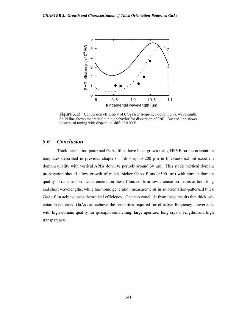
141
CHAPTER 5: Growth and Characterization of Thick Orientation-Patterned GaAs
5.6 Conclusion
Thick orientation-patterned GaAs films have been grown using HPVE on the orientation
templates described in previous chapters. Films up to 200 µm in thickness exhibit excellent
domain quality with vertical APBs down to periods around 30 µm. This stable vertical domain
propagation should allow growth of much thicker GaAs films (>500 µm) with similar domain
quality. Transmission measurements on these films confirm low attenuation losses at both long
and short wavelengths, while harmonic generation measurements in an orientation-patterned thick
GaAs film achieve near-theoretical efficiency. One can conclude from these results that thick ori-
entation-patterned GaAs can achieve the properties required for effective frequency conversion,
with high domain quality for quasiphasematching, large aperture, long crystal lengths, and high
transparency.
Figure 5.12: Conversion efficiency of CO2 laser frequency doubling vs. wavelength.Solid line shows theoretical tuning behavior for dispersion of [20]. Dashed line showstheoretical tuning with dispersion shift of 0.0003.
0
1
2
3
4
5
6
9 9.5 1 0 10.5 1 1
SH
G e
ffici
ency
( x
10-5
/W)
fundamental wavelength (µm)
CHAPTER 5: Growth and Characterization of Thick Orientation-Patterned GaAs
142
References
1. L.A. Eyres, P.J. Tourreau, T.J. Pinguet, C.B. Ebert, J.S. Harris, M.M. Fejer, B. Gerard, and E.
Lallier, "Quasi-phasematched frequency conversion in thick all-epitaxial, orientation-pat-
terned GaAs," Advanced Solid State Lasers, OSA Trends in Optics and Photonics Vol. 34, H.
Injeyan, U. Keller, and C. Marshall, eds. (Optical Society of America, Washington, DC, 2000)
pp. 259-261.
2. L.A. Eyres, P.J. Tourreau, T.J. Pinguet, C.B. Ebert, J.S. Harris, M.M. Fejer, L. Becouarn, B.
Gerard, and E. Lallier, "All-epitaxial fabrication of thick, orientation-patterned GaAs films
for nonlinear optical frequency conversion," Appl. Phys. Lett. 79, 904-906 (2001).
3. G.B. Stringfellow, Organometallic Vapor-Phase Epitaxy: Theory and Practice (Academic
Press, San Diego, 1999).
4. J.M. Durand, "Influence of the growth parameters in GaAs vapour phase epitaxy," Philips J.
Res. 34, 177-210 (1979).
5. J.L. Gentner, "Vapour phase growth of GaAs by the chloride process under reduced pressure,"
Philips J. Res. 38, 37-76. (1983).
6. L. Hollan, J.M. Durand, and R. Cadoret, "Influence of the growth parameters in GaAs vapor
phase epitaxy," J. Electrochem. Soc. 124, 135-139 (1977).
7. D.W. Shaw, "Kinetic aspects in the vapour phase epitaxy of III-V compounds," J. Cryst.
Growth 31, 130-141 (1975).
8. E. Gil-Lafon, J. Napierala, D. Castelluci, A. Pimpinelli, R. Cadoret, and B. Gerard, "Selective
growth of GaAs by HVPE: keys for accurate control of the growth morphologies," J. Cryst.
Growth 222, 482-496 (2001).
9. F. Chavez, J. Mimila-Arroyo, F. Bailly, and J.C. Bourgoin, "Epitaxial GaAs by close space
vapor transport," J. Appl. Phys. 54, 6646-6651 (1983).
10. F. Bailly, G. Cohen-Solal, and J. Mimila-Arroyo, "Simplified theory of reactive close-spaced
vapor transport," J. Electrochem. Soc. 126, 1604-1608 (1979).
11. N. Pütz, E. Veuhoff, K.-H. Bachem, P. Balk, and H. Luth, "Low pressure vapor phase epitaxy
of GaAs in a halogen transport system," J. Electrochem. Soc. 128, 2202-2206 (1981).
12. M. Yoshida, H. Terao, and H. Watanabe, "Thermodynamic and experimental study of low
pressure Ga/AsCl3/H2 VPE," (1986).
13. J. Napierala, E. Gil-Lafon, D. Castelluci, A. Pimpinelli, and B. Gerard, "Control of the growth
morphologies of GaAs stripes grown on patterned substrates by HVPE," Optical Mater. 17,
315-318 (2001).

143
CHAPTER 5: Growth and Characterization of Thick Orientation-Patterned GaAs
14. E. Gil-Lafon, J. Napierala, D. Castelluci, A. Pimpinelli, B. Gerard, and D. Pribat, "Kinetic
modelling of the selective epitaxy of GaAs on patterned substrates by HVPE. Application to
the conformal growth of low defect density GaAs layers on silicon," III-V and IV-IV Materi-
als and Processing Challenges for Highly Integrated Microelectronics and Optoelectronics,
Mater. Res. Soc. Symp. Proc. 140, S.A. Ringel, E.A. Fitzgerald, and I. Adesida, eds. (Materi-
als Reseach Society, Pittsburgh, PA, 1998) pp. 33-38.
15. Y. Li and L.J. Giling, "A closer study on the self-annihilation of antiphase boundaries in
GaAs epilayers," J. Cryst. Growth 163, 203-211 (1996).
16. T.J. Pinguet, O. Levi, T. Skauli, L.A. Eyres, L. Scaccabarozzi, M.M. Fejer, J.S. Harris, T.J.
Kulp, S. Bisson, B. Gerard, L. Becouarn, and E. Lallier, "Characterization of 0.5 mm thick
films of orientation-patterned GaAs for nonlinear optical applications," Conference on Lasers
and Electro-Optics, OSA Trends in Optics and Photonics (TOPS) Vol. 56 (Optical Society of
America, Washington, DC, 2001) p. 138.
17. J.I. Pankove, Optical Processes in Semiconductors (Prentice-Hall, Englewood Cliffs, NJ,
1971).
18. S.R. Johnson and T. Tiedje, "Temperature dependence of the Urbach edge in GaAs," J. Appl.
Phys. 78, 5609-5613 (1995).
19. T.J. Pinguet, personal communication to L. Eyres (2001).
20. A.N. Pikhtin and A.D. Yaskov, "Dispersion of the refractive index of semiconductors with
diamond and zinc-blende structures," Sov. Phys. Semicond. 12, 622-625 (1978).

CHAPTER 5: Growth and Characterization of Thick Orientation-Patterned GaAs
144

145
CHAPTER 6: High Power Operation and Future Devices
6.1 Introduction
With the successful demonstrations of the preceeding chapters, we can now explore
opportunities and limitations for nonlinear optical devices employing orientation-patterned GaAs
crystals. Orientation-patterned GaAs films now exist with excellent domain quality, proper phase-
matching periods for short wavelength pumping, large aperture, low attenuation losses and cm-
scale device lengths. This state of the art should allow operation of devices at low peak and aver-
age power levels such as the CW devices examined in chapter 2. Recent new results [1] have con-
firmed the usefulness of orientation-patterned GaAs for CW frequency conversion at low power
levels. DFG between 1.3 µm and 1.55 µm laser diodes produced 8-µm radiation with near the
expected theoretical efficiency and confirmed that the OPGaAs crystals were optically homoge-
neous and quasi-phasematchable over a 2 cm length. For many of the desired higher peak and
average power devices, however, several other previously unconsidered limitations which will
constrain device design and operation. In this chapter we will investigate these limitations and the
effects they will have on the performance of high power devices, including optical parametric
amplifiers and optical parametric oscillators.
6.2 Constraints on high power operation
The constraints on high-power frequency conversion fall into two categories, intrinsic lim-
itations and extrinsic limitations. Intrinsic limitations are inherent characteristics of the GaAs,
such as two-photon absorption. Extrinsic limitations are due to residual nonidealities in the GaAs
which may be improved in wavelength ranges of interest through improved fabrication processes,
such as optical scattering from crystal defects or absorption above the intrinsic levels set by the
Urbach tail and the phonon bands. The damage threshold could fall into either category, since one
can hypothesize both an intrinsic damage threshold and a lowered threshold due to crystal imper-
fections. This section will review the three effects most likely to limit high peak and average
power frequency conversion: the damage threshold, thermal effects associated with absorption,
and two-photon absorption.
CHAPTER 6: High Power Operation and Future Devices
146
6.2.1 Damage threshold
One unavoidable limit on the operation of nonlinear optical frequency conversion devices
is the threshold at which the crystals suffer physical damage from the optical radiation. Typically,
the endfacets are the most likely locations for such damage to occur. The damage properties of
GaAs at 2 µm have been measured by Peterson, et al. in conjunction with measurements of the
ZnGeP2 damage threshold [2]. The average damage threshold was observed to be 5.3 ± 1 J/cm2
for 70 ns pulses in both diffusion-bonded GaAs stacks and individual vertical-gradient-freeze
(VGF) GaAs wafer pieces in experiments with 2 µm beams which are well within the transparency
range and outside the range of two-photon absorption. All damage was observed on either the
front or rear surfaces of the GaAs crystals. Measurement was made by exposure of the sample to
10 pulses at the given energy level with damage detected by audible sounds or effects on transmis-
sion and confirmed by microscopic examination. In similar measurements on ZnGeP2, the authors
found that the energy threshold was approximately constant over a wide range of temporal pulse
lengths ranging from 150 ps to 200 ns, while for longer pulses (250 µs) the energy threshold
increased by two orders of magnitude. The authors speculate that if the energy is deposited faster
than a characteristic thermal relaxation time of the crystal (estimated to be in the 100s of µs
regime), the pulse format has little impact on the damage threshold and the damage depends on
energy deposition alone. Similar results were obtained in measurements on AgGaSe2 at the same
wavelength [3]. This seems the best assumption to use in the absence of explicit data for damage
threshold behavior in GaAs. Note, though, that there are some indications that this energy damage
threshold depends on the definition and experimental configuration. Lallier [4] observed damage
in GaAs crystals at over longer times with higher repetition rates that exhibited a lower damage
threshold than that observed by Peterson. There could be damage accumulation mechanisms
which serve to lower the damage threshold over time. Further investigation will be necessary to
elucidate these issues in the HVPE-grown GaAs crystals, since these damage mechanisms might
well depend on the processing history of the GaAs, crystal quality, and impurity concentrations.
6.2.2 Thermal effects
For high average power operation, thermal non-idealities can cause performance limita-
tions below those of the damage threshold. These thermal effects are caused by absorption of the
radiation from the pump beams and can affect both the beam quality and the phasematching uni-
formity. Optical absorption at the pump or other frequencies will lead to thermal gradients across
the beam which produce thermal lensing through the thermo-optic effect. Such a thermal gradient

147
CHAPTER 6: High Power Operation and Future Devices
across the beam can also cause phasematching variations across the beam which reduce the non-
linear gain. Thermal gradients along the length of the crystal due to significant pump absorption
can also limit the useful crystal length. Any detailed analysis of thermal effects on the conversion
efficiency in parametric devices is beyond the scope of this dissertation, so we will instead try to
understand the performance of GaAs-based frequency conversion devices by comparing their
probable performance with that of ZnGeP2, which has similar nonlinear and thermal properties.
Bordui and Fejer [5] examine these deleterious thermal effects and develop two figures of merit
which quantify the impact of thermal gradients across the beam on phasematching and thermal
lensing, respectively. In the simplest model, the amount of thermal dephasing across a Gaussian
beam is proportional to the pump power independent of beam size, while the focal length of an
induced thermal lens is proportional to the pump beam intensity (Power/beam area). The magni-
tude of the thermal dephasing normalized to the mixing efficiency provides one figure of merit
, (6.1)
while the magnitude of the thermal lensing normalized to the mxing efficiency yields another
. (6.2)
In these expressions, is the thermal conductivity, is the temperature depen-
dece of the dispersion of the refractive indices, and is the dependence of the refractive
index on temperature. For comparison of these figures of merit we take the ZnGeP2 absorption at
2 µm to be 0.09 cm-1 [6] and the OPGaAs 2 µm absorption to be 0.034 cm-1, which is the attenua-
tion value recently measured at 1.55 µm [7] where the attenuation is observed to be decreasing
with increasing wavelength. This attenuation value probably has a significant contribution from
scattering, which would not contribute to the thermal load, so the actual thermal performace of
OPGaAs will most likely be even better than this analysis indicates. The remainder of the mate-
rial constants were obtained from [5] including the for ZnGeP2 of 4.4*10-6 K-1 (calcu-
lated from the 40 cm-K temperature tuning bandwidth) with the exception of the for
FOMTDdeff
2 kth
α pumpn2 ∆n∂T∂
---------
-----------------------------------=
FOMTLkth
α pump T∂∂n
--------------------------=
kth ∆n∂ T∂⁄
n∂ T∂⁄
∆n∂ T∂⁄
∆n∂ T∂⁄

CHAPTER 6: High Power Operation and Future Devices
148
SHG of 4 µm radiation in GaAs which was recently measured to be ~1.5*10-5 K-1 [8]. Table 6.1
shows the thermal FOMs for the both GaAs and ZnGeP2.
The thermal dephasing FOMs are comparable for GaAs and ZnGeP2, while the GaAs
thermal lensing FOM is ~5x larger than that for ZnGeP2. The similarity of these coefficients for
GaAs and ZnGeP2 indicates that GaAs-based nonlinear optical devices should behave similarly to
or better than those based on ZnGeP2 in high power operation. This is fortunate, because ZnGeP2
has proven very robust in frequency conversion at high average power levels. Perhaps the most
impressive devices have been high power 2 µm-pumped OPOs. Generation of > 10 W of mid-IR
output has been demonstrated in a ZnGeP2-based OPO pumped by 20 W at 2 µm [9]. The conver-
sion efficiency was linear with pump power up to the 20 W pump power level with a 0.79 mm
diameter beam waist, exhibiting none of the saturation behavior which has been observed at the 3-
5 W (1 mm and 2 mm pump beam diameters, respectively) pump power levels in similar 2-µm-
pumped room temperature AgGaSe2 OPOs [10]. This saturation in AgGaSe2 OPOs was deter-
mined to be caused by thermal lensing [11]. Given the properties of GaAs and the linear depen-
dence of the thermal lensing on pump intensity, one would expect a GaAs OPO to operate without
significant thermal lensing effects at average pump intensities several times greater than those
already demonstrated in ZnGeP2 ( 8 kW/cm2). Similarly, since the thermal dephasing depends
linearly on the pump power, one could expect GaAs to handle average pump power levels in
excess of 20 W at 2 µm without suffering degredation in conversion efficiency. More detailed
thermal analysis is not warranted until the contributions of absorption and scattering to the total
attenuation can be separated and further investigation into the HVPE growth of OPGaAs eluci-
dates the practical lower bound on the absorption. In any case, these calculations indicate that
OPGaAs should exhibit excellent robustness in high power operation.
6.2.3 Two-photon absorption
GaAs exhibits two photon absorption (TPA) at wavelengths between the band edge and
one half of the bandgap energy, so that the absorption depends on the intensity according to
material FOMTD [GW*(pm/V)2] FOMTL [µW]
GaAs 0.46 0.95
ZnGeP2 0.45 0.022
Table 6.1: Thermal figures of merit of GaAs and ZnGeP2.

149
CHAPTER 6: High Power Operation and Future Devices
(6.3)
where is the TPA coefficient. For high peak power devices, this nonlinear scaling of absorption
with intensity leads to significant constraints on device design and operation to prevent excessive
absorption of pump radiation and associated deleterious thermal effects as discussed in the pre-
ceeding section. Figure 6.1 shows the TPA coefficient for GaAs as a function of wavelength taken
from the model of Van Stryland, et al. [12]. Unfortunately, in the range of attractive 1-µm pump
lasers, the TPA coefficient is between 20 cm/GW and 25 cm/GW, with a somewhat lower value of
12 cm/GW around 1.55 µm. Beyond 1.7-µm wavelength, the half-bandgap, TPA is naturally
absent and presents no constraints on device design. Note that while the linear attenuation is typi-
cally an extrinsic characteristic for GaAs in the wavelength range of interest, being dependent on
the concentrations of impurities, free carriers and physical defects which contribute to optical scat-
tering, TPA is an intrinsic characteristic and therefore is not modifiable by improvements in crystal
fabrication. The limitations on device performance associated with TPA can only be lifted by a
change in material, for example by shifting the bandgap in moving to a ternary alloy like AlGaAs
or to a different semiconductor like ZnSe or GaP. More detailed examination of the bound-elec-
tronic and free-carrier nonlinearities in GaAs can be found in [13].
Plane waves propagating through GaAs in the wavelength range of TPA will be attenuated
according to
Figure 6.1: TPA coefficient as a function of wavelength for GaAs.Model comes from [12].
α total I( ) α p βI+=
β
0
5
1 0
1 5
2 0
2 5
3 0
1 1.2 1.4 1.6 1.8 2
β(c
m/G
W)
wavelength (µm)

CHAPTER 6: High Power Operation and Future Devices
150
, (6.4)
with the optical intensity incident on the crystal, is the linear power attenuation, and the
distance through the medium. For crystals with low linear attenuation levels we can expand the
exponentials to first order to obtain
. (6.5)
Ignoring the effects of linear absorption for the moment, one sees that with a TPA coefficient of
20 cm/GW, and an incident intensity of 50 MW/cm2, half of the incident power will be absorbed in
passing through a 1 cm long crystal. The effects of this absorbed power on nonlinear optical fre-
quency conversion will depend on the actual power absorbed, but could contribute to both the
damage and thermal effects. For a Gaussian beam, this effect is somewhat more complicated than
for the plane wave, since the higher intensity center of the beam will be preferentially attenuated
and the resulting beam profile will no longer be gaussian. The same effect will preferentially heat
the central region of the gaussian beam and enhance any deleterious thermal lensing behavior.
TPA also affects the pulse nonuniformly in time as well as space and serves to flatten the temporal
shape. As a result of this non-uniform attenuation, the fraction of absorped pump power is smaller
for gaussian pulses than for plane waves. Figure 6.2 shows the transmission of incident pump
intensity/energy for plane waves, gaussian beams, and gaussian pulses in the presence of TPA.
Clearly, one must remain in the regime where < 1 to prevent significant pump absorption.
6.3 Device modeling
This section models the performance of frequency-conversion devices including OPAs
and OPOs pumped in both the non-TPA and TPA regimes. The thresholds are then compared to
the limitations placed by the mechanisms of the preceeding section to evaluate feasibility of these
devices. Along with the thermal effects caused by additional absorption of the pump radiation,
TPA will produce gain saturation due to preferential attenuation of the highest intensity portions of
the pump. For the calculations in this section, we make the simplifying assumption that the entire
pump beam is attenuated by the same factor. This approximation is justified because the gain in a
I z( )I0
α pz( )βI0
α p
-------- α pz( ) 1–exp( )+exp
---------------------------------------------------------------------------------=
I0 α p z
I z( )I0
1 α pz βI0z+ +-----------------------------------≈
βI0z

151
CHAPTER 6: High Power Operation and Future Devices
high-gain parametric device is confined largely to the regions of high pump intensity. Addition-
ally, this approximation has the benefit of overestimating the effects of TPA and thus providing an
upper bound on the effect of TPA on the performance of the device.
6.3.1 OPA/OPG
The wide transparency range of GaAs through the mid-IR makes it attractive for paramet-
ric amplification of signal wavelengths in the mid-IR spectral region. With sufficient gain (G ~
1010) amplification of vacuum noise to macroscopic levels is even possible so that no input signal
is required to generate signal and idler beams whose photon energies sum to that of the pump. To
produce these high gains required for OPG, short pump pulses and high intensities are typically
required. For pump wavelengths > 1.7 µm (or half the bandgap), this intensity will be limited only
by the damage threshold and possible deleterious thermal effects. For shorter pump wavelengths,
the intensities and gain will be limited severely by TPA.
In the absence of pump absorption, the gain in a parametric amplifier or OPO can be cal-
culated by solving the two coupled equations
Figure 6.2: Theoretical transmission of GaAs as function of two-photon absorption.The three curves show the transmission of a uniform plane wave as described byequation 6.4, the integrated power transmission over a gaussian transverse profile, andthe power transmission of a pulse with gaussian transverse and temporal profile.
0
0.2
0.4
0.6
0.8
1
0 0.5 1 1.5 2
% tr
ansm
issi
on
β
Gaussian pulse
2-D Gaussian
uniform plane wave
I0z

CHAPTER 6: High Power Operation and Future Devices
152
(2.6a)
. (2.6b)
For the case with input at only the signal wavelength, taking and neglecting pump deple-
tion, one calculates a signal gain of
(6.7)
for the phasematched case, where the gain is defined as
, (6.8)
is the pump intensity defined as and and are the wavelengths of the
signal and idler respectively. For large gains one can approximate the cosh function as an expo-
nential, so that the expression for gain in dB can be simplified to
. (6.9)
For a 2-µm pump wavelength and degenerate parametric amplification in GaAs, this high
gain approximation is
, (6.10)
a value which varies only slowly as one moves away from degeneracy. We assume here that the
nonlinearity is 96 pm/V, which is scaled using Miller’s rule from the 90 pm/V we used for 10.5 µm
frequency doubling. Additionally, throughout this chapter we assume the type I phasematching
configuration described in Chapter 2 in which .
With the extremely short pulses used to obtain very large parametric gains, the useable
crystal length is limited by group velocity walkoff. We can gain some idea of the behavior of such
a short-pulse device by looking at short-pulse harmonic generation. For a degenerate OPA, the
group walkoff length will be equal to the group walkoff length for second harmonic generation.
Imeshev, et al. [14] investigated the effects of group-velocity mismatch on quasi-phasematched
conversion efficiency and defined a figure of merit for confocal SHG
, (6.11)
where is the group velocity mismatch parameter defined as
dEs
dz--------
α x
2-----Es+ jκ sEpEi∗=
dEi
dz--------
α i
2-----Ei+ jκ iEpEs∗=
α s α i=
G L( )Es L( ) 2
Es 0( ) 2------------------- α sL–( )coshexp 2 ΓL( )= =
Γ 2 8π2deff2 I p
n1n2n3cε0λ sλ i
----------------------------------=
I p I p ncε0Ep2 2⁄= λ s λ i
G dB( ) 8.68ΓL 6–≈
G dB( ) 4.4 3–×10
W---------------------
I pL 6–≈
deff 2d14 3⁄=
FOMUFdeff
2
cn1n2δν--------------------=
δν
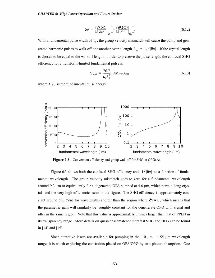
153
CHAPTER 6: High Power Operation and Future Devices
. (6.12)
With a fundamental pulse width of , the group velocity mismatch will cause the pump and gen-
erated harmonic pulses to walk off one another over a length . If the crystal length
is chosen to be equal to the walkoff length in order to preserve the pulse length, the confocal SHG
efficiency for a transform-limited fundamental pulse is
(6.13)
where is the fundamental pulse energy.
Figure 6.3 shows both the confocal SHG efficiency and as a function of funda-
mental wavelength. The group velocity mismatch goes to zero for a fundamental wavelength
around 9.2 µm or equivalently for a degenerate OPA pumped at 4.6 µm, which permits long crys-
tals and the very high efficiencies seen in the figure. The SHG efficiency is approximately con-
stant around 500 %/nJ for wavelengths shorter than the region where , which means that
the parametric gain will similarly be roughly constant for the degenerate OPO with signal and
idler in the same region. Note that this value is approximately 3 times larger than that of PPLN in
its transparency range. More details on quasi-phasematched ultrafast SHG and DFG can be found
in [14] and [15].
Since attractive lasers are available for pumping in the 1.0 µm - 1.55 µm wavelength
range, it is worth exploring the constraints placed on OPA/OPG by two-photon absorption. One
Figure 6.3: Conversion efficiency and group walkoff for SHG in OPGaAs.
δν k ω( )dωd
---------------ω1
k ω( )d
ωd---------------
ω2
–=
τ1
Lgv τ1 δν⁄=
η conf76.7
ε0λ13
----------FOMUFUFH=
UFH
0
500
1000
1500
2000
2 3 4 5 6 7 8 9 1 0conv
ersi
on e
ffici
ency
(%
/nJ)
fundamental wavelength (µm)
0.1
1
1 0
100
1000
2 3 4 5 6 7 8 9 1 0
1/|δ
ν|(m
m/p
s)
fundamental wavelength (µm)
1 δν⁄
δν 0≈
CHAPTER 6: High Power Operation and Future Devices
154
can solve the same two coupled equations 6.6a and 6.6b with the pump distribution in the crystal
given by equation 6.5 to obtain an approximation for the power gain of a plane wave at the signal
wavelength in the presence of TPA and under the condition to be
, (6.14)
which clearly reduces to equation 6.5 in the absence of pump absorption. Figure 6.4 shows this
parametric gain for a 1-µm pump in OPGaAs and various crystal lengths neglecting absorption at
the pump, signal and idler wavelengths to observe the constraints placed by TPA alone. The
dashed lines show the gain without TPA, while the solid lines include the effects of TPA. The grey
lines are constant intensity-length contours corresponding to absorption of some frac-
tion of the total incident pump radiation in the nonlinear crystal. Even for long crystals (4 cm),
only relatively low gains (< 102) are achiveable for . In the presence of linear absorption
at the pump wavelength, the achieveable gains are correspondingly reduced. The limitations on
intensity mean that long crystals are preferred for short wavelength pumping, since they allow the
same gains with lower pump intensities. Pumping at 1.55 µm instead of 1.064 µm increases only
slightly (~ 3 dB) the gains achieveable before one reaches the same values of and the
TPA-related absorption. TPA clearly places significant limitations on the achieveable parametric
gain in the crystal. For this reason, short wavelength pumping in GaAs will be useful primarily for
low gain amplifiers, such as power amplifiers and OPOs, rather than for high gain applications
such as OPG. Note that large gains are possible with long crystals and high intensities, but these
devices will suffer from large amounts of pump absorption and associated thermal effects which
will limit the repetition rates. Additionally, high pump intensities in this wavelength range may
also encounter complications from other nonlinear effects such as the nonlinear index of refrac-
tion.
6.3.2 OPOs
For OPO operation we again have the same pump wavelength regimes in which TPA is
either absent or present. Considering first the case without TPA, one can use the method of Byer
and Brosnan [16] to estimate pulsed SRO thresholds. For each trip around the OPO cavity during
signal buildup, the signal beam is amplified or attenuated by
, (6.15)
α s α i=
G L( ) Es L( )Es 0( )--------------
2α sL–( )coshexp 2 2Γ
α p βI0+( )------------------------- 1 α p βI0+( )L+ 1–( )= =
∆ βI0L=
∆ 0.1<
∆ βI0L=
Pm
Pm 1–------------ RG t L,( )=

155
CHAPTER 6: High Power Operation and Future Devices
where is the single-pass gain through the nonlinear crystal and is the round-trip reflec-
tivity of the cavity mirrors at the signal wavelength. For the case with linear absorption at the
pump wavelength given by equation 6.4 with , the solution of equations 6.6a and 6.6b gives
a single pass gain of
, (6.16)
where is given by
, (6.17)
and quantifies the spatial coupling between the nonlinear polarization and the cavity mode
according to
, (6.18)
thus assuming the near-field focusing discussed in Sections 2.1.2 and 2.3.1. Starting from noise
input levels, equation 6.16 can easily be numerically integrated from the noise level over many
Figure 6.4: Parametric gain in OPGaAs pumped at 1.06 µm vs. pump intensity.The solid curves show OPGaAs samples of varying lengths, while the dashed curvesshow gain without TPA. The grey curves are plots of constant indicatingmagnitude of TPA. Linear absorption is neglected.
0
20
40
60
80
100
120
0 5 10 15 20
para
met
ric g
ain
in d
B
Pump intensity (MW/cm2)
4 cm
2 cm
1 cm
∆=1.0
∆=0.5
∆=0.1
∆ βI0L=
G t L,( ) R
β 0=
G t L,( ) α sL–( )coshexp 2 Γ t( )α p
---------- α pL–( ) 1–exp( )=
Γ t( )
Γ 2 8π2deff2 gsI p t( )
n1n2n3cε0λ sλ i
----------------------------------=
gs
gs
wp2
wp2 ws
2+------------------=

CHAPTER 6: High Power Operation and Future Devices
156
round trips in the cavity during the assumed gaussian temporal pump pulse shape to the approxi-
mately µJ level we define as the threshold. The pump intensity is assumed constant during a sin-
gle pass through the crystal for simplicity. Figure 6.5 shows the energy threshold of a 2-µm-
pumped SRO generating an 8-µm idler for which the idler polarization is set to be confocal in the
crystal in the same manner as was done for the DFG calculations of Chapter 2, since we use the
same near-field approximation. Pump and signal beams are assumed to have the same waist diam-
eter and are set by the constraint on the idler polarization. The threshold calculations could be
extended to tighter focusing conditions using an approach like that of Guha, et al. [17] or Boyd
and Kleinman [18] as discussed in Chapter 2, but the confocal idler case provides sufficient results
for our purposes. The cavity is a bow-tie ring configuration to minimize the round-trip losses by
only passing once through the OPGaAs crystal and is assumed 1 cm longer than the crystal on
each end of the cavity. Each of the four mirrors is taken to have a reflectivity of R=0.99 at the sig-
nal wavelength and be perfectly transmitting at the pump and idler wavelengths, while the crystal
is assumed to be antireflection coated at all wavelengths. The attenuation at pump, signal and idler
wavelengths is assumed to be the same.
The threshold pump energies extend down to ~11 µJ (22 mJ/cm2 * cm2; see
equation 2.7 and the following paragraph for the definition of effective area) for a 4-cm-long
OPGaAs crystal and 50-ns pulses. Attenuation losses of 0.034 cm-1 at 1.55 µm have been
observed in OPGaAs for periods shorter than those required for 2 µm pumping, indicating that the
Figure 6.5: Threshold fluence of 2-µm-pumped OPO generating an 8 µm idler. Losses are assumed the same at all three wavelengths and the idler polarization is set tobe confocal in the OPGaAs crystal.
0
2 0
4 0
6 0
8 0
100
0.01 0.02 0.03 0.04 0.05
Thr
esho
ld fl
uenc
e (m
J/cm
2)
absorption loss
10 ns
50 ns
10 ns
50 ns
2 cm crystal
4 cm crystal
wpump
=0.125 mm
wpump
=0.176 mm
4.9 4–×10

157
CHAPTER 6: High Power Operation and Future Devices
range of operation of Figure 6.5 is realistic. We conclude that OPGaAs OPOs can achieve thresh-
old at fluences more than two orders of magnitude below the 5.1 J/cm2 material damage threshold
at 2 µm discussed above. If the damage threshold under high-frequency pulsed operation is even
an order of magnitude lower than this value, there should still be room to operate such low-thresh-
old fluence OPOs. Examining thermal effects, assuming a OPGaAs OPO with 2-cm-long crystal
and an ~ 80 mJ/cm2 threshold were pumped to 5x over threshold to achieve high conversion effi-
ciency, such an OPO could run at a repetition rate of 20 kHz before exceeding the 8 kW/cm2 inten-
sity value at which ZnGeP2 with comparable thermal figures of merit exhibited no thermal
degradation. Since the peak pump threshold intensity will remain constant as the OPO is scaled
proportionally to higher power levels by increasing the beam sizes and since the thermal lens focal
length scales with the intensity, thermal lensing should thus not be an issue, even at high repetition
rates. We can conclude that for OPOs pumped at wavelengths outside the TPA regime, the large
cushions between these threshold fluences and both the optical damage threshold and the thermal
degredation regime leave significant room for optimization of OPO characteristics and adaptation
to various engineering constraints. This is not surprising, since GaAs has comparable nonlinear
gain and thermal properties to ZnGeP2, which has been utilized for a wide range of mid-IR OPO
applications.
At pump wavelengths below 1.7 µm, the practical pump intensities for an OPGaAs OPO
will be constrained by TPA. Because an OPO can utilize multiple passes to achieve large gains,
these constraints are somewhat less limiting than is the case for OPA devices. There are a variety
of attractive pump sources available in the 1-µm-wavelength range; it is an interesting question
whether or not such a 1-µm-pumped OPGaAs OPO is feasible. In the case with TPA, the gain for
each round trip through the cavity is given by
. (6.19)
Figure 6.6 shows the threshold intensity of a 1-µm-pumped OPO generating directly an 8-µm idler
as a function of the absorption at pump, signal and idler beams, which is again assumed to be
equal. The OPO parameters and calculational method are the same as in the 2-µm-pumped case,
with . The solid lines show the calculation using equation 6.19, which includes
the assumption of small linear absorption at the pump wavelength, while the dashed curves show
an upper bound on the threshold employing equation 6.16 with the approximation that
. The idler polarization is again set to be confocal in the 4-cm-long OPGaAs
Pm
Pm 1–------------ R α sL–( )coshexp 2 2Γ t( )
α p βI0+( )------------------------- 1 α p βI0+( )L+ 1–( )=
β 23 cm/GW=
α p' α p βI0+( )=

CHAPTER 6: High Power Operation and Future Devices
158
crystal. The thresholds for 10-ns and 50-ns pulse widths are shown along with the CW threshold
for the same device for comparision.
The gain approximation for low pump absorption and the upper bound agree well in the
regions of low absorption losses, as expected, and diverge more for larger absorption losses.
Clearly long crystals and long pulses are optimal, since they lower the intensity threshold. Thresh-
old intensities down to 0.2 MW/cm2 can be obtained with 50 µs pulses and 0.005 cm-1 absorption
with . Achievement of significant conversion efficiency will require pumping
several times over threshold, which will push operation into the regime where TPA will absorb
non-negligible amounts of the pump radiation. Further reductions in threshold are possible by
increasing the pulse length, since the CW threshold can be an order of magnitude smaller
(~20 kW/cm-2), but this feasibility of this strategy depends strongly on the attenuation. The 1-µm-
pumped OPO feasibility will depend strongly on the absorption losses in the OPGaAs crystals.
Losses at 1 µm were recently measured to be ~ 0.1 cm-1 at 1.064 µm in an orientation-patterned
GaAs film [7], though this was on a sample having somewhat longer periods (27 µm) than those
required for 1-µm pumping (8 µm - 15 µm) and is is not clear how the losses will scale with
domain period. However, with low-loss crystals, long crystal lengths, and proper pulse formats,
operation of a 1-µm-pumped OPGaAs OPO appears possible.
Figure 6.6: Threshold intensity for 1-µm-pumped OPO vs. GaAs absorption loss.Loss is assumed the same at all three wavelengths. OPGaAs crystal is 4-cm-long andOPO generates an 8 µm idler. Solid curves are threshold intensity with theapproximation for low pump absorption of equation 6.19, while dashed curves show anupper bound.
0
0.5
1
1.5
2
0.02 0.04 0.06 0.08 0.10
0.04
0.08
0.12
0.16
Pea
k th
resh
old
pum
p in
tens
ity (
MW
/cm
2 )
absorption loss at pump, signal and idler (cm-1)
∆=
Ι 0βz
cw
10 ns
20 ns
50 ns
∆ βIoL 0.02= =

159
CHAPTER 6: High Power Operation and Future Devices
Figure 6.7 shows similar peak threshold intensities for 1.55 µm pumping and varying
OPGaAs crystal length with the attenuation at all wavelengths set to 0.034 cm-1, which was the
value measured at 1.55 µm wavelength for 27-µm domain periods. Here the TPA coefficient is
approximately a factor of 2 smaller (12 cm/GW) than that for a 1 µm pump wavelength. This
reduction widens the window for OPO operation below TPA-related complication. Since these
required periods have been demonstrated and the losses at 1.55 µm measured, this devices can be
considered realistic, even at the present state of OPGaAs development. The ideal source for
pumping such OPGaAs OPOs would be a quasi-CW source with long pulses, thus allowing pump-
ing close to the CW threshold without the thermal loading required of true CW operation. Unfor-
tunately, such lasers are more difficult to obtain than standard Q-switched lasers with shorter
pulses. This pulse format may be achieveable using a master oscillator/power amplifier configura-
tion instead of a directly Q-switched laser.
6.4 Conclusion
This chapter examined the major limitations on performance of high-peak-power devices
in GaAs, including damage threshold, thermal effects, and two-photon absorption. OPA gain will
be limited when pumped by 1-µm lasers, but suffers no such restrictions for pump wavelengths
greater than 1.7 µm. OPO operation will be possible with 2-µm pumping for which there are large
Figure 6.7: Threshold intensity for 1.5-µm-pumped OPO vs. GaAs crystal length.Loss of 0.034 cm-1 is assumed at all three wavelengths and OPO generates an 8 µmidler.
0
1
2
3
4
5
1 1.5 2 2.5 3 3.5 40
0.01
0.02
0.03
0.04
0.05
0.06
peak
thre
shol
d pu
mp
inte
nsity
(M
W/c
m2 )
OPGaAs crystal length (cm)
10 ns
20 ns
40 ns
100 ns
CW
Ι 0β(c
m-1)
CHAPTER 6: High Power Operation and Future Devices
160
margins between threshold and the relevant damage and thermal limitations. 1-µm-pumped OPOs
look feasible in theory, but will depend on the magnitude of the attenuation losses achievable in
OPGaAs with the proper domain periods.

161
CHAPTER 6: High Power Operation and Future Devices
References
1. O. Levi, T.J. Pinguet, T. Skauli, L.A. Eyres, L. Scaccabarozzi, M.M. Fejer, J.S.J. Harris, T.J.
Kulp, S. Bisson, B. Gerard, L. Becouarn, and E. Lallier, "Mid-infrared generation by differ-
ence-frequency mixing in orientation-patterned GaAs," Conference on Lasers and Electro-
Optics, OSA Trends in Optics and Photonics (TOPS) Vol. 56 (Optical Society of America,
Baltimore, MA, 2001).
2. R.D. Peterson, K.L. Schepler, J.L. Brown, and P.G. Schunemann, "Damage properties of
ZnGeP2 at 2 µm," J. Opt. Soc Am. B 12, 2142-2146 (1995).
3. B.C. Ziegler and K.L. Schepler, "Transmission and damage threshold measurements on
AgGaSe2 at 2.1 µm," Appl. Opt. 30, 5077-5080 (1991).
4. E. Lallier, personal communication to L. Eyres (2000).
5. P.F. Bordui and M.M. Fejer, "Inorganic crystals for nonlinear optical frequency conversion,"
Annu. Rev. Mater. Sci. 23, 321-379 (1993).
6. P.G. Schunemann and T.M. Pollak, "Ultralow gradient HGF-grown ZnGeP2 and CdGeAs2
and their optical properties," MRS Bulletin 23, 23-27 (1998).
7. T.J. Pinguet, O. Levi, T. Skauli, L.A. Eyres, L. Scaccabarozzi, M.M. Fejer, J.S. Harris, T.J.
Kulp, S. Bisson, B. Gerard, L. Becouarn, and E. Lallier, "Characterization of 0.5 mm thick
films of orientation-patterned GaAs for nonlinear optical applications," Conference on Lasers
and Electro-Optics, OSA Trends in Optics and Photonics (TOPS) Vol. 56 (Optical Society of
America, Washington, DC, 2001) p. 138.
8. T. Skauli, personal communication to L. Eyres (2001).
9. P.A. Budni, L.A. Pomeranz, M.L. Lemons, P.G. Schunemann, T.M. Pollak, and E.P. Chicklis,
"10 W mid-IR holmium pumped ZnGeP2 OPO," Advanced Solid State Lasers, OSA Trends in
Optics and Photonics (TOPS) Vol. 19, W.R. Bosenberg and M.M. Fejer, eds. (Optical Society
of America, Washington, DC, 1998) pp. 226-229.
10. P.A. Budni, M.G. Knights, E.P. Chicklis, and K.L. Schepler, "Kilohertz AgGaSe2 optical
parametric oscillator pumped at 2 µm," Opt. Lett. 18, 1068-1070 (1993).

CHAPTER 6: High Power Operation and Future Devices
162
11. C.L. Marquardt, D.G. Cooper, P.A. Budni, M.G. Knights, K.L. Schepler, R. DeDomenico,
and G.C. Catella, "Thermal lensing in silver gallium selenide parametric oscillator crystals,"
Appl. Opt. 33, 3192-3197 (1994).
12. E.W. Van Stryland, S. Guha, H. Vanherzeele, M.A. Woodall, and M.J. Soileau, "Verification
of the scaling rule for two-photon absorption in semiconductors," Optica Acta 4, 381-386
(1986).
13. A.A. Said, M. Sheik-Bahae, D.J. Hagan, T.H. Wei, J. Wang, J. Young, and E.W. Van Stryland,
"Determination of bound-electronic and free-carrier nonlinearities in ZnSe, GaAs, CdTe, and
ZnTe," J. Opt. Soc Am. B 9, 405-414 (1992).
14. G. Imeshev, M.A. Arbore, M.M. Fejer, A. Galvanauskas, M. Ferman, and D. Harter,
"Ultrashort-pulse second-harmonic generation with longitudinally nonuniform quasi-phase-
matching gratings: pulse compression and shaping," J. Opt. Soc Am. B 17, 304-318 (2000).
15. G. Imeshev, M.M. Fejer, A. Galvanauskas, and D. Harter, "Pulse shaping by difference-fre-
quency mixing with quasi-phase-matching gratings," J. Opt. Soc Am. B 18, 534-539 (2001).
16. S.J. Brosnan and R.L. Byer, "Optical parametric oscillator threshold and linewidth studies,"
IEEE J. Quantum Electron. QE-15, 415-431 (1979).
17. S. Guha, F.J. Wu, and J. Falk, "The effects of focusing on parametric oscillation," IEEE J.
Quantum Electron. QE-18, 907-912 (1982).
18. G.D. Boyd and D.A. Kleinman, "Parametric interaction of focused gaussian light beams," J.
Appl. Phys. 39, 3597-3639 (1968).

163
CHAPTER 7: Summary
In the introduction to this dissertation, as at the beginning of the research described within
it, we identified a number of applications for nonlinear optical frequency conversion in the near-
and mid-IR, including countermeasures, remote sensing, and spectroscopy, as well as communica-
tions applications, such as WDM frequency conversion in the near-IR. Since these frequency con-
version devices are typically limited by the performance of the nonlinear optical crystals used in
their implementation, device engineers are always looking for advances in materials properties and
fabrication which can improve the optical device performance. We also identified that GaAs and
related zincblende semiconductor materials have excellent characteristics for applications in non-
linear optical frequency conversion, including large nonlinearities, an appealing transparency
range for mid-IR generation, and a large thermal conductivity, along with compatibility with
waveguide fabrication techniques. The only limitation was that of phasematching, since these iso-
tropic semiconductors have no birefringence for phasematching and previous techniques for fabri-
cating periodically-oriented GaAs materials proved difficult and yielded only short crystal lengths.
7.1 Accomplishments
7.1.1 Materials fabrication
At the heart of this dissertation lies the invention and demonstration of all-epitaxial tech-
niques for fabricating orientation-patterned semiconductor films, particuarly GaAs and AlGaAs.
Using MBE to perform polar-on-nonpolar epitaxy, we investigated the proper parameters for GaAs
growth on Ge and obtained the required crystal inversion in a heteroepitaxial GaAs/Ge/GaAs
structure, solving antiphase domain complications along the way. Using these inverted GaAs het-
erostructures, we developed MBE-regrowth-compatible selective etching techniques and demon-
strated all-epitaxial orientation-patterned templates. The domain periods demonstrated on these
templates were sufficient to achieve quasiphasematching of any collinear frequency conversion
process in the transparency range of GaAs/AlGaAs. We demonstrated growth of orientation-pat-
terned thin and thick GaAs and AlGaAs films by a variety of techniques including HVPE and
MBE. HVPE films had thicknesses up to 500 µm with excellent domain quality down to periods
of 27 µm, while the MBE films had thickness up to 5 µm with excellent domain quality down to

CHAPTER 7: Summary
164
periods of 3.25 µm. The domains propagated vertically through the film with large aspect ratios
under both HVPE and MBE growth conditions.
7.1.2 Optical characterization
The thick GaAs films exhibit good optical transmission at both long and short wave-
lengths, with losses ≤ 0.1 cm-1 measured for the proper phasematching periods in the near-IR
wavelength range attractive for pumping mid-IR generation. Harmonic generation measurements
on these films found conversion efficiencies comparable those predicted theoretically. For
waveguide devices, the efficiencies were limited by the large propagation losses of ~ 40 dB/cm and
harmonic generation efficiencies were measured to be consistent with these losses.
7.2 State-of-the-art
Our materials and optical experiments show that orientation-patterned GaAs now meets
all of the basic requirements for nonlinear optical frequency conversion and that it should be con-
sidered a promising candidate for application in mid-IR frequency conversion applications. For
the thick GaAs materials in particular, we have simultaneously demonstrated a useful aperture
(0.5 mm) high domain quality, proper domain periods for phasematching near-IR pumped fre-
quency conversion, useful crystal lengths (2 cm), and good optical transmission at both near-IR
and mid-IR wavelengths. Combining these with the attractive intrinsic material characteristics of
high nonlinearity, high thermal conductivity and high damage threshold, GaAs appears poised to
move quickly into applications by drawing on the vast accumulated knowledge about semiconduc-
tor growth and properties. Achievement of the same factors (aperture, poling, crystal length, etc.)
in periodically-poled lithium niobate led quickly to demonstration of a plethora of nonlinear opti-
cal devices. We have seen from theoretical calculations that GaAs offers attractive possibilities
for CW DFG, low threshold optical parametric oscillators, and high average power OPOs, particu-
larly for conversion to beyond > 9.0 µm where ZnGeP2 begins to exhibit absorption. It also has
the major advantage of being pumpable by well-developed near-IR lasers in the 1 µm - 2 µm
wavelength range.

165
CHAPTER 7: Summary
7.3 Future work
Ongoing work in orientation-patterned GaAs will need to focus on several areas, including
materials growth, optical properties, device modeling, and device demonstration. One of the most
important issues is improving the orientation-template fabrication process. This will allow smaller
template corrugations, which should produce lower defect densities in both bulk and waveguide
devices. For waveguide devices, it will also be important to eliminate any corrugations which
develop during regrowth, whether due to faceted growth or template defects. For bulk OPGaAs,
investigation into the domain interruptions and pyramidal defects should result in higher domain
quality and make possible growth of shorter period films for use with 1-µm pump lasers. Extend-
ing growth to thicker (>1 mm) apertures is also attractive and will probably occur in conjunction
with the improvements in film quality.
Determining the sources of attenuation loss in both bulk and waveguide materials is
extremely important, since the magnitude of these losses will determine the ultimate performance
of the devices. The contributions of absorption and scattering will need to be understood and that
information fed back to the crystal growth process to reduce these parasitic effects to the minimum
possible levels. More detailed measurements of the optical properties of bulk materials, both
absorption and dispersion, will be necessary to allow accurate device modelling. Eliminating
residual ambiguity in the magnitude of the nonlinear susceptibility would also be helpful.
Many devices are presently being demonstrated in OPGaAs, including difference fre-
quency generators and optical parametric oscillators. For near-IR-pumped operation, more
detailed modelling of devices operating in the presence of two-photon absorption will be necessary
to optimize performance. Waveguide device performance might be greatly improved by the design
of waveguide structures resistant to corrugation-related scattering losses. As the performance of
these devices improves, they can move out of the research environment and into practical applica-
tions such as spectroscopy, remote sensing, and countermeasures. Such testing under realistic
device conditions will be necessary to verify thermal limitations and uncover any additional non-
idealities affecting device operation.
Further into the future, since these devices utilize quasiphasematching, a variety of
chirped or dispersion-tailored devices can be envisioned for applications such as pulse compres-
sion or tunable mid-IR generation. These orientation-patterned growth techniques could also be
extended into other material systems to take advantage of properties like the extremely wide trans-
parency range and low loss of ZnSe, or the potentially wide-bandwidth, mid-IR amplification pos-

CHAPTER 7: Summary
166
sible with near-IR pump wavelengths using GaP. The larger bandgaps of these materials would
also eliminate complications with two-photon absorption.
Overall, the research in this dissertation demonstrates that orientation-patterned semicon-
ductor materials hold great promise for nonlinear optical frequency conversion. Further research
into materials growth, optical properties, and devices is now required to turn that promise into a
reality.

167
CHAPTER 7: Summary