akustica - carnegie mellon universityjzhu/class/18200/f05/lecture05_gabriel.pdf · microphone...
TRANSCRIPT

Akustica
Dr. Kaigham (Ken) J. GabrielChairman & CTO
Akustica, Inc. • 2835 East Carson Street • Suite 301 • Pittsburgh, PA 15203 USA • 412-390-1730 • www.akustica.com

© Akustica, Inc. - Proprietary & Confidential 2
What if integrated circuits
could hear, speak and sense the
world around them?

© Akustica, Inc. - Proprietary & Confidential 3
Akustica Improves Voice Quality
Microphones, speakers and complete
acoustic systems on a single MEMS
chip …… enabling cell phones, laptops
and other electronic devices to
speak, hear, and feel.
Better Microphone Technology …
Digital and directionalmicrophones
…with Integrated Voice Processing ...
Algorithms to suppress wind and background noise
… and Multi-Sensor Clusters
Detect vibration interference and extract noise

© Akustica, Inc. - Proprietary & Confidential 4
Sensory Silicon™
Patented CMOS MEMS technology enables systemPatented CMOS MEMS technology enables system--onon--chip integration of multiple chip integration of multiple
sensors, electronics, and signal processing.sensors, electronics, and signal processing.
Microphones
Analog / Mixed SignalElectronics: Amplifiers,
A/D Converters
Signal Processing
Inertial Sensors
MicrophoneMicrophone
and Speaker Chips
++
++
++
and Speaker Chips
CMOS
MEMS Sensor ClustersSensor Clusters
© Akustica, Inc. - Proprietary & Confidential 5
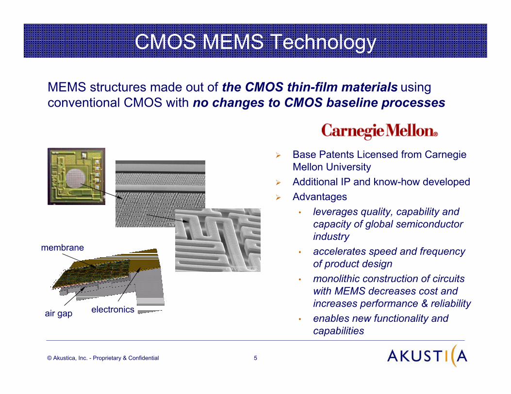
CMOS MEMS Technology
MEMS structures made out of the CMOS thin-film materials usingconventional CMOS with no changes to CMOS baseline processes
membrane
air gap electronics
Base Patents Licensed from Carnegie Mellon University
Additional IP and know-how developed
Advantages
• leverages quality, capability and
capacity of global semiconductor
industry
• accelerates speed and frequency
of product design
• monolithic construction of circuits
with MEMS decreases cost and
increases performance & reliability
• enables new functionality and
capabilities

© Akustica, Inc. - Proprietary & Confidential 6
Initial Products
AKU1000 – Analog Output Microphone
Monolithic silicon microphoneSurface mount to improve manufacturing yieldAutomated pick & place saves assembly cost 2X smaller footprint / thinner profile than ECMProduction ramp - Now
AKU2000 – Digital Output Microphone
Integrated 14-bit, 4th-order - modulatorMonolithic solution for superior transducerperformance (10X lower parasitics)Immune to RF and EM interference enablingincreased audio design flexibilityProduction ramp – Q4

© Akustica, Inc. - Proprietary & Confidential 7
Large and Growing Installed Market
Microphone Market ForecastMicrophone Market Forecast
MEMS CAGR = 98%MEMS CAGR = 98%
On an annual basis, global OEMs On an annual basis, global OEMs andand ODMsODMs purchase:purchase:
•• 1.5 B microphones1.5 B microphones
•• 3.0 B near3.0 B near--field speakersfield speakers
MEMS microphones are rapidly replacing conventional ECMs(~100M units in ’05)
• MEMS microphones rapidly adopted into mobile handsets
• >500m MEMS microphones forecasted for 2008
• Attractive pricing and margin opportunities
Secured high volume analog silicon microphone supply contract
Units (000,000)Units (000,000)
0
500
1,000
1,500
2,000
2004 2005 2006 2007 2008
ECM MEMS

© Akustica, Inc. - Proprietary & Confidential 8
Target Markets
Communications – Smart Phones
Enable next-generation handsets: thinner, smaller, lighter phones with better directionality, noise cancellation & fidelity
Cell phones that sound great in noisy environments
Moving to digital bus architecture
Personal Computing - NotebooksImproved voice conferencing in VoIP applicationsEnable full utilization of next generation Intel hardware and Microsoft softwareRequire the addition of multiple microphones in displays for multi-media speaker-phone applications
Digital Media – Consumer ElectronicsRaise audio quality to correspond to high quality videoComponent reduction enables smaller devices such as headsetsEnables rich new uses of sound in cameras, voice recorders, and other consumer devices

© Akustica, Inc. - Proprietary & Confidential 9
Notebooks Usage Case Evolution
officeworkstation
distributed collaboration
integrated servicesplatformremote
workstation
© Akustica, Inc. - Proprietary & Confidential 10
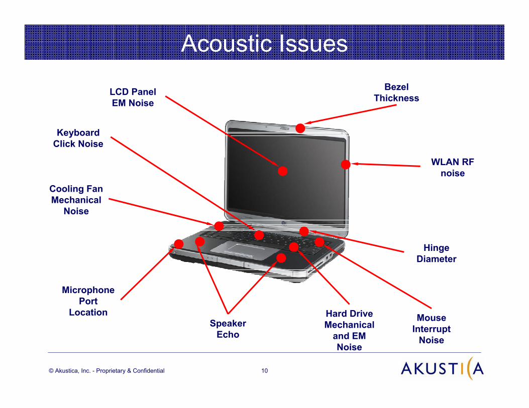
Acoustic Issues
Hinge
Diameter
Bezel
ThicknessLCD Panel
EM Noise
Cooling Fan
Mechanical
Noise
Speaker
Echo
Mouse
Interrupt
Noise
WLAN RF
noise
Hard Drive
Mechanical
and EM
Noise
Keyboard
Click Noise
Microphone
Port
Location

© Akustica, Inc. - Proprietary & Confidential 11
Akustica Overcomes The Challenges
FLEXIBILITY AND MANUFACTURABILITY
Digital Microphones enable ideal placement in bezel• Noise susceptibility is reduced• Allows signal transfer through the hinge• Silicon technology enables very thin and small footprint• Digital architecture reduces customization and calibration in assembly
Reduced component count and cost
• Integrated pre-Amp• Simple ribbon
cable interconnect
Requires an HD Audio CODEC that has a direct interface to digitalmicrophones
© Akustica, Inc. - Proprietary & Confidential 12
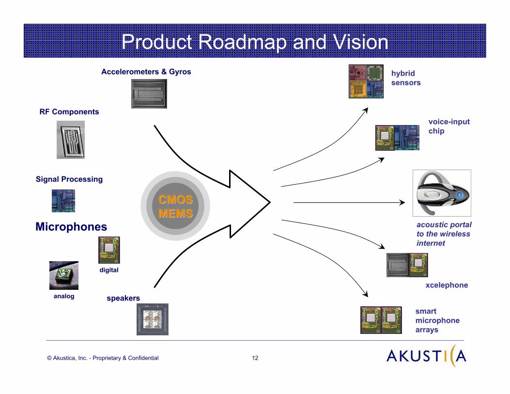
Product Roadmap and VisionAccelerometers & Gyros
RF Components
Signal Processing
Microphones
speakers
digital
CMOSCMOS
MEMSMEMSacoustic portal
to the wireless
internet
smart
microphone
arrays
hybrid
sensors
voice-input
chip
xcelephone
analog

© Akustica, Inc. - Proprietary & Confidential 13
Company Profile
HQ in Pittsburgh, PA USA
Formed in 2001 by Ken Gabriel and Jim Rock
Carnegie Mellon University Patents & Akustica IP
42 Employees, 80% Engineers
Private, Venture-Backed ($30M)
Commercializing CMOS MEMS for Major Consumer Electronic Applications

Emerging Trends in ECE
CMOS Microelectromechanical
Systems (CMOS MEMS)
The Power of Many
Dr. Kaigham (Ken) J. Gabriel
Chairman & CTOAkustica, Inc.
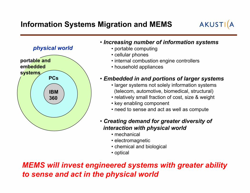
Information Systems Migration and MEMS
• Increasing number of information systems• portable computing• cellular phones• internal combustion engine controllers• household appliances
• Embedded in and portions of larger systems• larger systems not solely information systems
(telecom, automotive, biomedical, structural)• relatively small fraction of cost, size & weight• key enabling component• need to sense and act as well as compute
• Creating demand for greater diversity of
interaction with physical world• mechanical• electromagnetic• chemical and biological• optical
physical world
IBM
360
PCs
portable and
embedded
systems
MEMS will invest engineered systems with greater ability
to sense and act in the physical world
MEMS
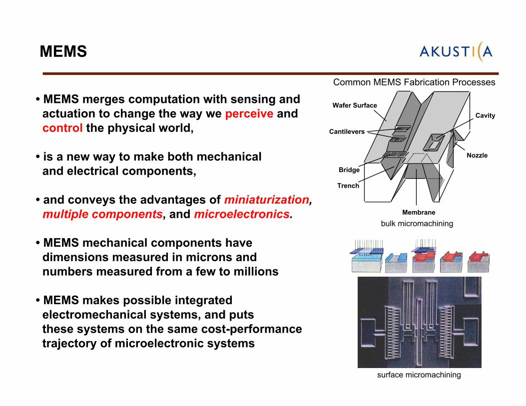
Common MEMS Fabrication Processes
bulk micromachining
Trench
Bridge
Cantilevers
Wafer Surface
Cavity
Nozzle
Membrane
• MEMS merges computation with sensing and
actuation to change the way we perceive and
control the physical world,
• is a new way to make both mechanical
and electrical components,
• and conveys the advantages of miniaturization,
multiple components, and microelectronics.
• MEMS mechanical components have
dimensions measured in microns and
numbers measured from a few to millions
• MEMS makes possible integrated
electromechanical systems, and puts
these systems on the same cost-performance
trajectory of microelectronic systems
surface micromachining

Surface Micromachined Structure

MEMS Builds on Microelectronics Manufacturing
DEPOSITIONOF
MATERIAL
PATTERNTRANSFER
REMOVALOF
MATERIAL
COMPUTER-AIDEDDESIGN, SIMULATIONAND LAYOUT OFDEVICE
GENERATION OFPHYSICAL MASKS OR DIRECT-WRITEPATTERNS
CONCEPTION OF NEW DEVICE;SPECIFICATION OF PROCESS
MULTIPLE PROCESSING CYCLES
free-form geometries
3D solid modelers
coupled electrical, mechanical,
fluidic, kinematic ... analysis
thicker films
deeper etches
fewer steps
removal of underlying
materials to release
mechanical parts
PROBETESTING
SECTIONINGINDIVIDUAL
DIEASSEMBLY
INTO PACKAGEPACKAGE
SEALFINALTEST
special probing, sectioning and handling
procedures to protect released parts
seal some parts of device
but expose others
test more than
electrical function
Microelectronics & MEMS Fabrication
Wafer lot
(~20-25 wafers)
100-300 mm
1-3 mm
0.5-1.0 mm
Wafer
DieDevice
(4 - 12 in)

Economics of Batch Fabrication
High manufacturing cost is spread over many parts-- low cost per
individual part
Die size and total process yield (= product individual process step
yields) are the two most important determinants of part cost
0 2 4 6 8
D = wafer diameter [inches]
N = number of parts/batch ~ 127 D2
(2.5 mm2 dice, 25 wafers/batch, $10k/batch)
1
10
100
1000
10000
400100
100010,000
$1
$10
$100
$1000
$5
$8
$2$0.22
10 12

Present and Emerging Applications of MEMS
• inertial measurement units on a chip for personal guidance, toys, virtual reality, munitions
guidance, and security/safety systems
• distributed unattended sensors for asset tracking, structural assessment, environmental
monitoring, security & border surveillance, and process control
• integrated fluidic systems for miniature analytical instruments, chip-based DNA processing
& sequencing, propellant and combustion control, chemical factories on chip
• radio frequency and wireless for relay & switching matrices, reconfigurable antennas,
switched filter banks, electromechanical front-end RF filtering and demodulation
• embedded sensors and actuators for condition-based maintenance of machines &
vehicles, on-demand amplified structural strength in lower-weight systems/platforms and
disaster-resistant buildings
• mass data storage devices for storage densities of terabytes per square centimeter
• integrated micro-optomechanical components for fiber optic telecommunications
switching networks, optical data storage, bar code scanning and displays
• active, conformable surfaces for distributed aerodynamic control of aircraft,
adaptive optics, and precision parts & material handling

Acceleration Sensor on a Chip for Airbags
applied
acceleration
• single mechanical component
with ~ 200 transistors
(3 µm design rules)
• monolithic sensing, self-test,
calibration and signal
conditioning functions
• manufactured in an integrated
circuit fabrication line like
any other type of
semiconductor chip
capacitive sensing
+/- 50 g full scale
DC to 1 kHz
5 volt supply
$10 in volume
ADXL-50
enables a family
of products
Analog Devices, Inc.
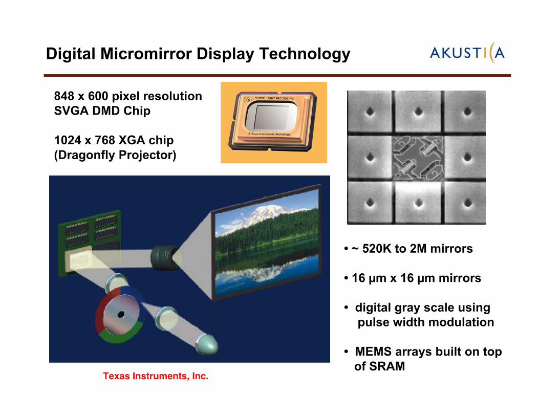
Digital Micromirror Display Technology
848 x 600 pixel resolution
SVGA DMD Chip
1024 x 768 XGA chip
(Dragonfly Projector)
• ~ 520K to 2M mirrors
• 16 µm x 16 µm mirrors
• digital gray scale using
pulse width modulation
• MEMS arrays built on top
of SRAMTexas Instruments, Inc.

Carnegie Mellon CMOS MEMS
Inertial sensors, RF MEMS, infrared sensors, acoustic speakers, ultrasonic sensors, BioMEMS, biomedical devices… with on-chip detection and conditioning
Integrated Systems on Chip
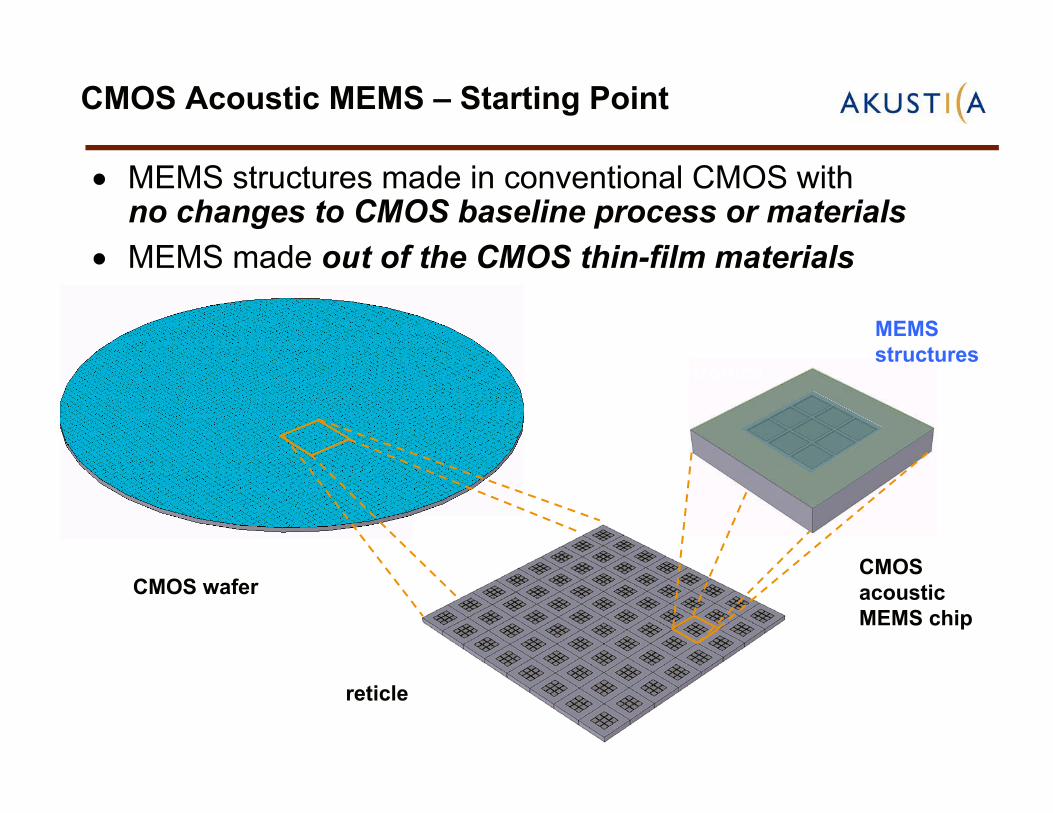
CMOS Acoustic MEMS – Starting Point
MEMS structures made in conventional CMOS withno changes to CMOS baseline process or materials
MEMS made out of the CMOS thin-film materials
CMOS wafer
reticle
CMOS
acoustic
MEMS chip
CMOS
electronics
MEMS
structures

Microphone Chip Example
front side of chip
back side of chip
single membrane
back cavity
vent hole array
membrane array
electronics
1 mm - 3 mm
1 mm - 3 mm

Membrane Mesh Scaffolding
mesh fabricated in metal and dielectrics
of CMOS process
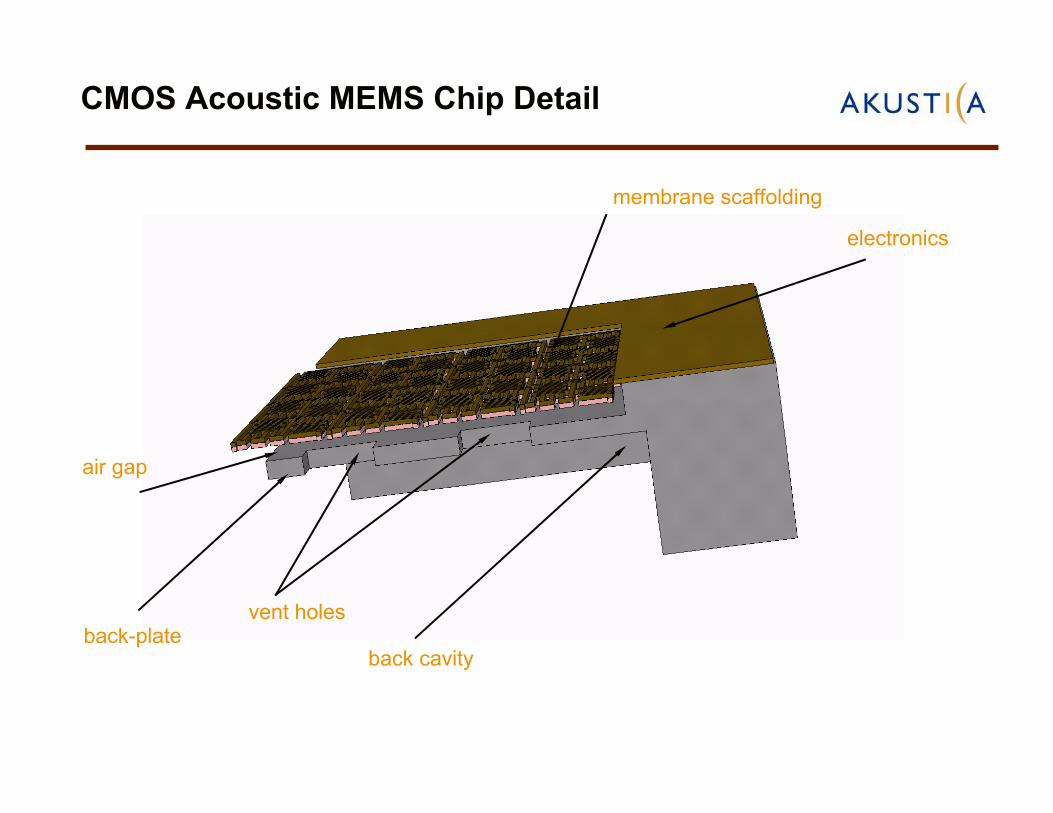
CMOS Acoustic MEMS Chip Detail
back cavity
vent holes
membrane scaffolding
electronics
air gap
back-plate

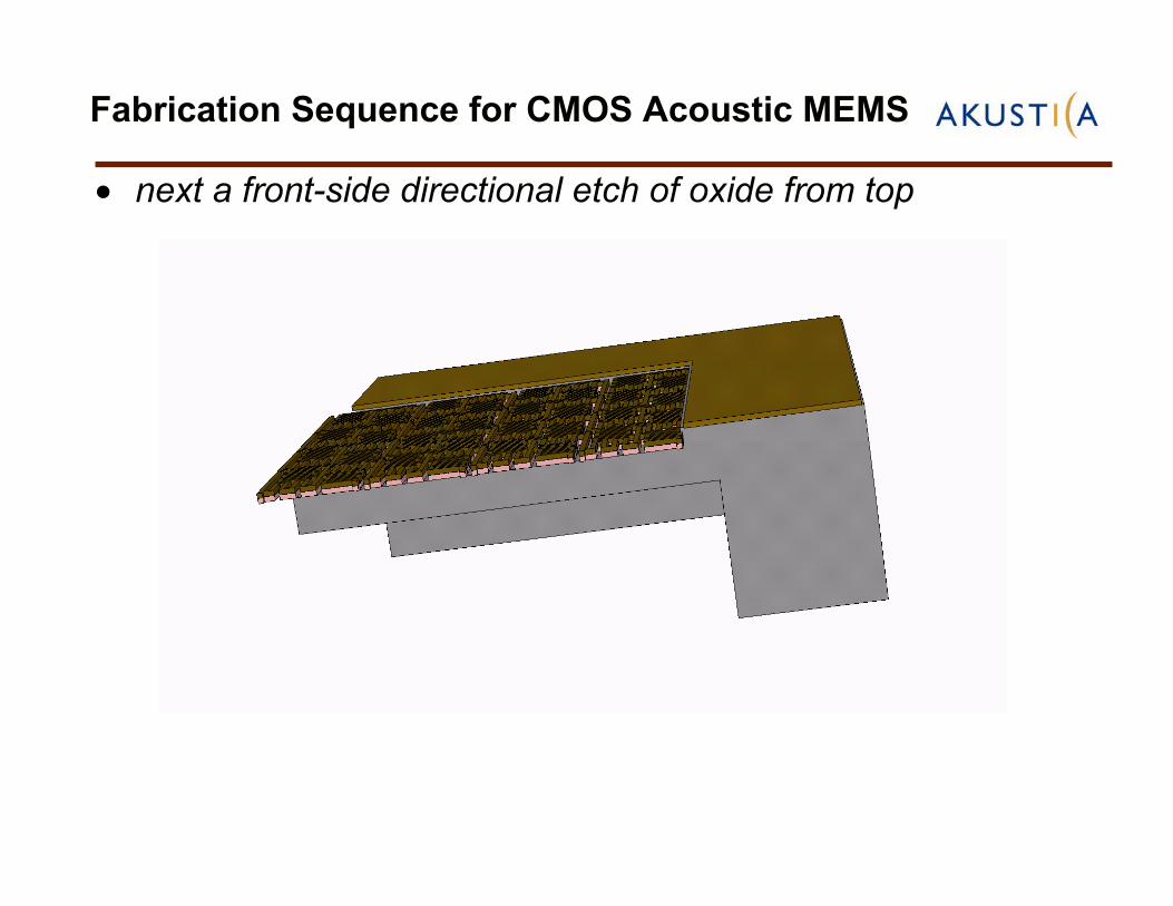
Fabrication Sequence for CMOS Acoustic MEMS
overglass
metal 3
chip as fabricated from CMOS fab
example 3-metal CMOS process
metal 1 mesh
oxide
silicon substrate
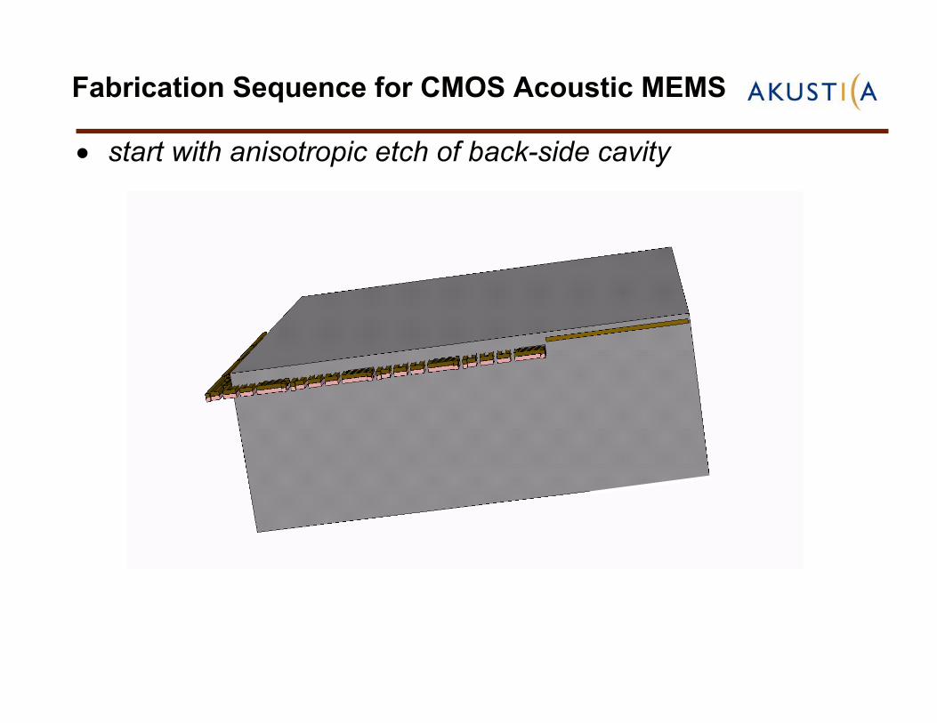
Fabrication Sequence for CMOS Acoustic MEMS
start with anisotropic etch of back-side cavity

Fabrication Sequence for CMOS Acoustic MEMS
start with anisotropic etch of back-side cavity

Fabrication Sequence for CMOS Acoustic MEMS
start with anisotropic etch of back-side cavity
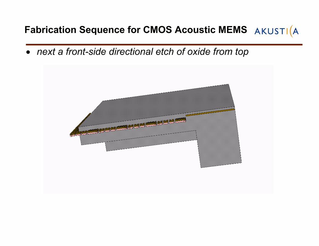
Fabrication Sequence for CMOS Acoustic MEMS
next a front-side directional etch of oxide from top
Fabrication Sequence for CMOS Acoustic MEMS
next a front-side directional etch of oxide from top

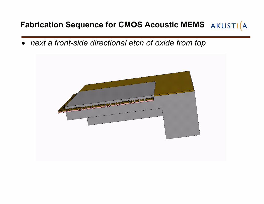
Fabrication Sequence for CMOS Acoustic MEMS
next a front-side directional etch of oxide from top
Fabrication Sequence for CMOS Acoustic MEMS
next a front-side directional etch of oxide from top

Fabrication Sequence for CMOS Acoustic MEMS
vent holes etched from top

Fabrication Sequence for CMOS Acoustic MEMS
vent holes etched from top

Fabrication Sequence for CMOS Acoustic MEMS
vent holes etched from top

Fabrication Sequence for CMOS Acoustic MEMS
mesh skeleton released from substrate underneath

Fabrication Sequence for CMOS Acoustic MEMS
mesh skeleton released from substrate underneath
Capacitanceto
VoltageConversion
VoltageAmplifier
+_ V
A
C =
d

SEMs of CMOS Acoustic MEMS Chip
back cavity
vent holes
electronics
membrane
air gap
back-plate
mesh skeleton

CMOS MEMS Microphone
Capacitanceto
VoltageConversion
VoltageAmplifier
+_ V
p(t)
A
C[t] =
d[p(t)]
v(t)

Microphone Chip Acoustic Model
Radiation Diaphragm
Backplate
Gap Vents
Volume/N
SoundPressure
U
+
P ~
acoustic
impedance
model for one
diaphragm of
microphone
array
100
101
102
103
104
105
10-5
10-4
10-3
10-2
C/C0 at 1 Pa
Frequency, Hz
| C
/C0|
C/C0 at 1 Pa of Input Pressure
predicted mechanical
frequency response of
microphone
-
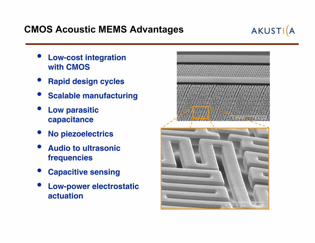
CMOS Acoustic MEMS Advantages
• Low-cost integration with CMOS
• Rapid design cycles
• Scalable manufacturing
• Low parasitic capacitance
• No piezoelectrics
• Audio to ultrasonic frequencies
• Capacitive sensing
• Low-power electrostatic actuation
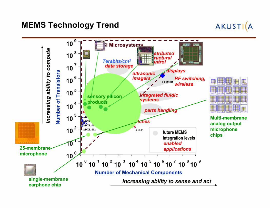
incre
asin
g a
bilit
y t
o c
om
pu
te
increasing ability to sense and act
future MEMS
integration levelsenabled
applications
Nu
mb
er
of
Tra
nsis
tors
Number of Mechanical Components
109
100
101
10
103
105
106
107
108
104
410
010
110
210
310
510
610
710
8
109
TI DMD
2
10
Terabits/cm2
data storage
inertial navigationon a chip
car,
consumer
optical switches & aligners
distributedstructuralcontrol
displays
parts handling
cellularrobotics
integrated fluidicsystems
ADXL-181 (mil)
ADXL-50
ADXL-05
ADXL-202
M3
SC
GLV
ultrasonicimagers RF switching,
wireless
VLSI Microsystems
MEMS Technology Trend
25-membrane
microphone
single-membrane
earphone chip
sensory silicon
products
Multi-membrane
analog output
microphone
chips