afm applications in polymer science and engineering · and advantages of asylum research cypher™...
TRANSCRIPT
1
The atomic force microscope (AFM) is a powerful tool for characterizing polymer materials. It provides nanoscale information on
a wide range of physical properties and behavior in addition to imaging morphology. This note describes the many capabilities
and advantages of Asylum Research Cypher™ and MFP-3D™ AFMs for understanding polymers.
AFM Applications in Polymer Science and Engineering
Polymers are the material of choice in many applications. They can be tailored to have unique properties and are often less expensive, more durable, and more sustainable than other materials. Creating and implementing new polymers requires knowledge of how structure, processing, properties, and performance are related. Understanding these effects at the molecular or microstructural level requires that this information be acquired with micro- and nanometer resolution.
Whether investigating fundamental principles of polymer science (Figure 1) or engineering a specific polymer solution (Figure 2), the AFM is a key instrument for evaluating polymers at small length scales [1-4]. Its spatial resolution enables visualization of sub-micrometer and sub-nanometer polymer morphology. But AFMs can contribute much more information about polymers besides simple topographic morphology, including probing molecular-level forces; mapping mechanical, thermal, and electrical properties; and assessing solvent and thermal effects in near real time.
Exploring Morphology and StructurePolymers have a rich hierarchy of structure on micro- and nanometer length scales. Smaller scale features include brush configuration and chain packing of single molecules, lamellae of crystalline polymers, and microphase separation in block or graft copolymers. Larger features are fillers or pores, interfacial phases in polymer blends, and effects of processing (e.g., strain, heat, etching) on surface roughness or finish. In addition, polymeric nanoparticles, nanofibers, and nanodevices require statistics on both individual and ensemble size and shape.
AFMAsylum Research
Figure 1: Morphology of PS-PEP diblock copolymer film – Tapping mode phase image of a polystyrene-block-poly(ethylene- alt-propylene) (PS-PEP) film on a silicon wafer. The darker region on the left side with lower phase corresponds to the high side of a 16 nm step in the wafer. In this region and the darker curved region on the right, the film forms a PS wetting layer. In the lighter region with higher phase, the film contains a single layer of spherical PEP microdomains. Several vertical rows of aligned microdomains are seen on the low side of the step. Diblock copolymers can self assemble into complex periodic structures, a property that has attracted interest for their use as templates in nanolithography. Understanding how film thickness and step height affect domain location and orientation aids in developing block copolymer templates. Imaged with the MFP-3D AFM; scan width 2 µm, Z (phase) scale 10°. Adapted from Ref. 5.
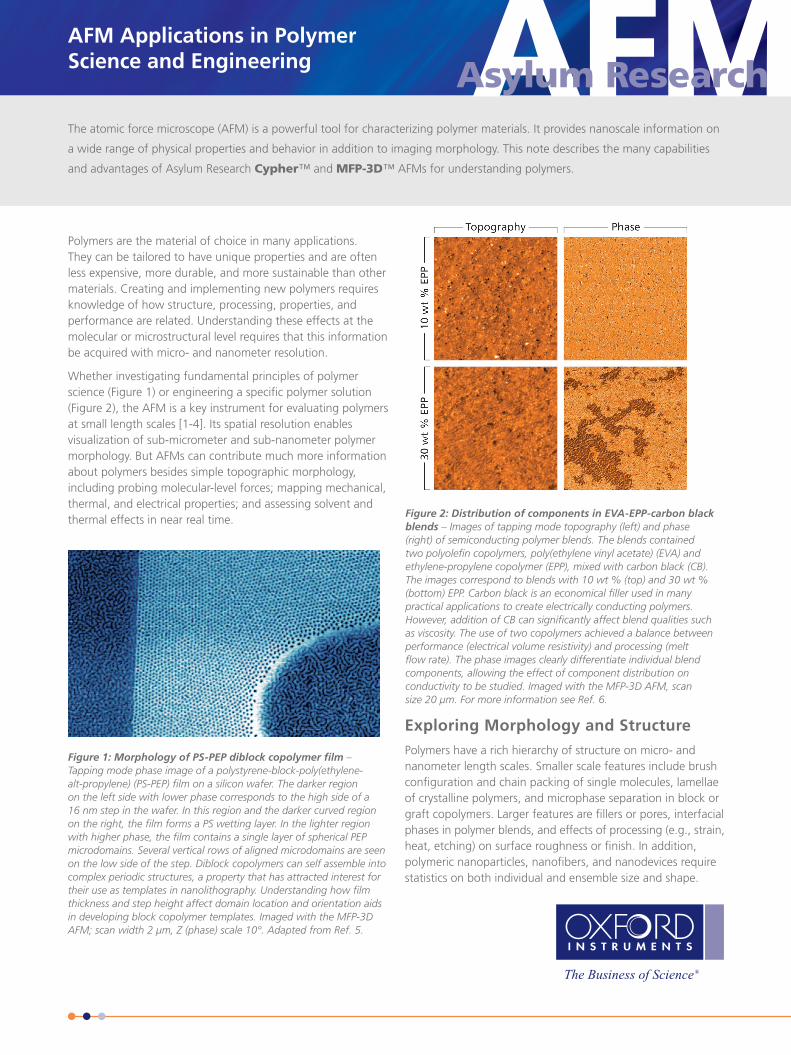
Figure 2: Distribution of components in EVA-EPP-carbon black blends – Images of tapping mode topography (left) and phase (right) of semiconducting polymer blends. The blends contained two polyolefin copolymers, poly(ethylene vinyl acetate) (EVA) and ethylene-propylene copolymer (EPP), mixed with carbon black (CB). The images correspond to blends with 10 wt % (top) and 30 wt % (bottom) EPP. Carbon black is an economical filler used in many practical applications to create electrically conducting polymers. However, addition of CB can significantly affect blend qualities such as viscosity. The use of two copolymers achieved a balance between performance (electrical volume resistivity) and processing (melt flow rate). The phase images clearly differentiate individual blend components, allowing the effect of component distribution on conductivity to be studied. Imaged with the MFP-3D AFM, scan size 20 µm. For more information see Ref. 6.

The AFM provides information on structure through nanoscale imaging of topography (height), which is usually acquired in tapping mode. Tapping mode images provide high spatial resolution, even resolving atomic and molecular structure (Figure 3). The high spatial resolution derives from the small tip-sample contact area in tapping mode, which is a product of ultrasharp probe tips as well as the extremely gentle lateral and vertical tip-sample forces in tapping mode.
In recent years the speed of AFM imaging has increased (Figure 4), due to the introduction of AFMs like the Asylum Research Cypher that support use of smaller cantilevers with higher resonant frequencies. Smaller cantilevers can also better resolve and control very low (sub-piconewton) forces, an important consideration for delicate, easily deformed polymers.
Asylum AFMs for Topographic Imaging
l All Asylum AFMs feature closed-loop scanners, which use position sensors to ensure accurate and repeatable scanning motion. This eliminates image distortions and enables high-precision offsets and zooms on specific scan areas. The Cypher S, Cypher ES, and MFP-3D Infinity™ feature the latest generation of position sensors with exceptionally low noise, as low as 35 pm in Z (vertical) and 60 pm in X and Y (lateral).
l Cypher family AFMs support small cantilevers (<10 µm long) for faster imaging, routinely operating at line scan rates of 10-40 Hz. Small cantilevers also provide noise and resolution benefits, such that imaging single point atomic defects and the DNA double helix is now routine.
l GetStarted™ makes tapping mode simple on the MFP-3D Infinity and Cypher family AFMs by automatically optimizing imaging parameters. A predictive algorithm is used to set parameters before the tip even touches the sample, ensuring that neither the tip nor sample is damaged by non-optimal settings and that high quality data is acquired from the first scan line.
Learn More
Webinar: “Smaller and Quieter: Ultra-High Resolution AFM Imaging”
Measuring Forces and DeformationThe inherently high force sensitivity of the AFM cantilever makes it well suited to measuring forces from piconewtons to micronewtons, a range that encompasses many polymer interactions. Force measurements are typically made in two ways: by pulling single molecules to probe molecular-level forces and by indenting polymeric materials to assess their elastic and viscoelastic response to deformation.
Single-molecule force spectroscopy involves stretching a molecule between the AFM tip and substrate and measuring the cantilever deflection. With knowledge of the cantilever’s spring constant and deflection sensitivity, a plot of force versus distance is obtained. Such force curves provide information about intramolecular forces (e.g., single-chain elasticity, conformational transitions) and intermolecular forces (e.g., polymer-solvent interactions, desorption or adhesion to surfaces) within, or between, single polymer molecules. Figure 5 shows an example of force spectroscopy measurements on molecules of poly-L-lysine as they desorb from a hydrophobic surface.
AFM Applications in Polymer Science and Engineering
2
Figure 3: Molecular and crystalline structure of rubrene – Tapping mode topography images of crystalline rubrene imaged with the Cypher S AFM. Rubrene is a polycyclic aromatic hydrocarbon used as an organic semiconductor in organic light emitting diodes. The main color image with scan size 5 µm shows single steps of the crystalline lattice. The inset black-and-white image reveals molecular-level structure, highlighting the superb spatial resolution of Cypher AFMs, even in air. Scan size 20 nm. Sample courtesy of Rutgers University.
Figure 4: PHB/V spherulite crystallization – Tapping mode phase images of a polyhydroxybutyrate-co-valerate (PHB/V) spherulite crystallizing at room temperature over a period of three minutes. Scan size 1.5 µm. The scan rate of 40 Hz, or approximately 10 seconds per frame, allows clear visualization of the crystallization process. Imaged with the Cypher AFM. Sample courtesy of the University of Sheffield.
See the movie
oxinst.com /phbv

AFM Applications in Polymer Science and Engineering
3
Similarly, AFM indentation measures the cantilever deflection as the tip is pushed into a sample. Conventional cantilevers can apply sufficient forces to deform polymers with modulus in the range from kilopascals to a few gigapascals. Analysis with a model for the tip-sample indentation yields information on the sample’s nanoscale elastic and viscoelastic properties.
Asylum AFMs for Force Measurements
l GetReal™ is a software feature on all Asylum AFMs that automatically calibrates the cantilever spring constant and deflection sensitivity with a single click, without ever touching the sample surface.
l All Asylum AFMs feature thermally-limited force measurements and low-noise Z sensors, meaning both axes of force curves are measured with the highest possible sensitivity and accuracy.
l All Asylum AFMs contain powerful analysis features for force curves. A variety of pre-programmed indentation models including Hertz/Sneddon, Johnson-Kendall-Roberts (JKR), Derjaguin-Müller-Toporov (DMT), and Oliver-Pharr are available as well as a model selection guide that includes plasticity index, force to adhesion ratio, and Tabor coefficient calculation.
l The NanoIndenter™ option for MFP-3D family AFMs replaces the AFM cantilever with a true instrumented vertical nanoindenter to make ISO 14577-compliant nanoindentation measurements.
Mapping Nanomechanical PropertiesMechanical properties of polymers are an important consideration in applications ranging from food packaging to flexible electronics. To optimize mechanical performance, one or more phase-separated components or fillers may be included. The length scales of such inclusions demand mechanical-property measurements with nanoscale spatial resolution. Asylum Research offers a wide range of techniques for investigating nanomechanical properties, ranging from simple qualitative techniques to more sophisticated quantitative methods. In many cases these techniques are complementary and can be used together to learn more about polymer samples.
Tapping mode with phase imaging was a source of much excitement beginning in the late 90s. Since then, phase imaging has become a valuable technique for polymer characterization, where it can often resolve fine structural details and discriminate various material components from each other. Interpretation is not always straightforward, however, because the phase response depends on how the material stores elastic energy and dissipates viscous energy (i.e., the loss tangent) as well as other dissipative forces. Notwithstanding these challenges, phase imaging remains a simple and popular means of obtaining qualitative material property contrast.
Bimodal imaging (Dual AC™) is another option for qualitative mapping of material property variations. It operates the same as regular tapping mode with phase imaging, except that an additional mode of the cantilever is driven simultaneously with operation at the first mode. The amplitude and phase response at this second mode is measured along with topography and phase from the first mode. Like regular phase imaging, interpretation of the results is not always easy, but the technique can be useful for obtaining contrast in cases where phase imaging does not provide it.
Among the techniques in Asylum’s NanomechPro™ Toolkit, the exclusive AM-FM Viscoelastic Mapping Mode is especially well suited to polymers. Similar to bimodal imaging, it uses tapping mode operating simultaneously at two different cantilever mode frequencies. However, the frequency of the second mode is tracked and related to the sample stiffness while the amplitude and phase of the first mode is related to the sample loss tangent. This enables unambiguous, quantitative mapping of elastic storage modulus and viscoelastic loss modulus or loss tangent, all with the usual speed and nondestructive nature of tapping mode. AM-FM Mode’s huge range of applicability— from less than 1 MPa to more than 100 GPa—means it can be used on virtually any polymer. An example of AM-FM mapping on a multicomponent polymer assembly is shown in Figure 6.
Figure 5: Single molecule forces for poly-L-lysine homopolymer – (top) Graphic of force spectroscopy concepts. A single polymer molecule is covalently attached to the AFM tip by a linker (here, polyethylene glycol, PEG). (bottom) Force-distance curve for poly-L-lysine on a hydrophobic self-assembled monolayer (SAM) in water. The force plateau indicates the desorption of a single polymer from the surface. Histograms obtained from multiple force curves provide the average desorption force (inset, top) and detachment length (inset, bottom). Acquired with the MFP-3D AFM. Adapted from Ref. 7.
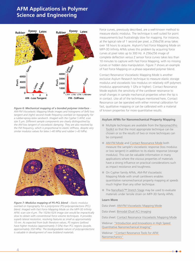
Force curves, previously described, are a well-known method to measure elastic modulus. The technique is well suited for point measurements but frustratingly slow for mapping. For instance, at the typical rate of 1 second per pixel, a 256x256 array takes over 18 hours to acquire. Asylum’s Fast Force Mapping Mode on MFP-3D Infinity AFMs solves this problem by acquiring force curves at pixel rates up to 300 Hz. A 256x256 image of complete deflection versus Z sensor force curves takes less than 10 minutes to capture with Fast Force Mapping, with no missing curves or hidden data manipulation. Figure 7 shows an example of Fast Force Mapping on a phase-separated polymer blend.
Contact Resonance Viscoelastic Mapping Mode is another exclusive Asylum Research technique to measure elastic storage modulus and viscoelastic loss modulus on relatively stiff polymers (modulus approximately 1 GPa or higher). Contact Resonance Mode exploits the sensitivity of the cantilever resonance to small changes in sample mechanical properties when the tip is in contact. Like all of the techniques mentioned here, Contact Resonance can be operated with either minimal calibration for fast, qualitative mapping or can be calibrated with a material of known properties for more quantitative results.
Asylum AFMs for Nanomechanical Property Mapping
l Multiple techniques are available from the NanomechPro Toolkit so that the most appropriate technique can be chosen or so the results of two or more techniques can be compared.
l AM-FM Mode and Contact Resonance Mode both measure the sample’s viscoelastic response (loss modulus or loss tangent) in addition to its elastic response (storage modulus). This can be valuable information in many applications where the viscous properties of materials have a strong influence on practical considerations such as impact resistance and toughness.
l On Cypher family AFMs, AM-FM Viscoelastic Mapping Mode with small cantilevers enables quantitative nanomechanical property mapping at speeds much higher than any other technique.
l The NanoRack™ Stretch Stage may be used to evaluate materials under tensile strain on MFP-3D family AFMs.
Learn More
Data sheet: AM-FM Viscoelastic Mapping Mode
Data sheet: Bimodal (Dual AC) Imaging
Data sheet: Contact Resonance Viscoelastic Mapping Mode
Webinar: “Introduction and Innovations in High Speed Quantitative Nanomechanical Imaging”
Webinar: “Contact Resonance Tools for AFM Nanomechanics”
AFM Applications in Polymer Science and Engineering
4
Figure 7: Modulus mapping of PS-PCL blend – Elastic modulus overlaid on topography for a polystyrene (PS)-polycaprolactone (PCL) blend. Imaged with Fast Force Mapping Mode on the MFP-3D Infinity AFM; scan size 4 µm. The 1024x1024 image size would be impractically slow to obtain with conventional force volume techniques. It provides superb lateral resolution, resolving features as small as approximately 10 nm. As expected from bulk literature values, PS regions (yellow) have higher modulus (approximately 3 GPa) than PCL regions (purple, approximately 350 MPa). The biodegradable nature of polycaprolactone is valuable in development of new bioblend materials.
Figure 6: Mechanical mapping of a bonded polymer interface – AM-FM Viscoelastic Mapping Mode images and histograms of (left) loss tangent and (right) second mode frequency overlaid on topography for a rubber-epoxy-latex sandwich. Imaged with the Cypher S AFM; scan size 5 µm. Different sample components are clearly distinguished by the AM loss tangent of viscoelastic damping. They are also resolved by the FM frequency, which is proportional to elastic stiffness, despite very similar modulus values for latex (~40 MPa) and rubber (~43 MPa).
Measuring Thermal PropertiesMany polymers exhibit dramatic property changes with temperature. Data such as glass transition temperatures are valuable for a fundamental understanding of molecular motion, to assess performance-critical properties like toughness and impact resistance, and to understand the effects of processing or operation at high temperatures.
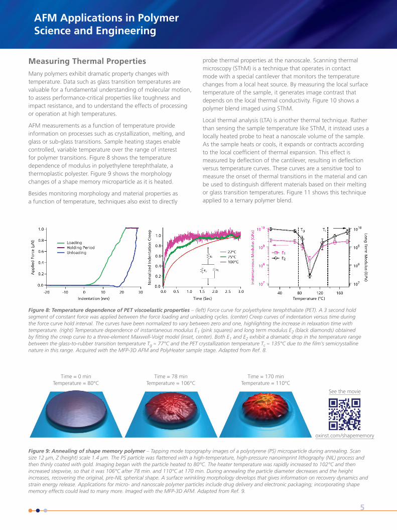
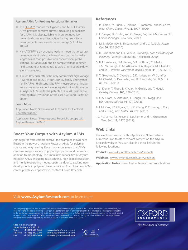
AFM measurements as a function of temperature provide information on processes such as crystallization, melting, and glass or sub-glass transitions. Sample heating stages enable controlled, variable temperature over the range of interest for polymer transitions. Figure 8 shows the temperature dependence of modulus in polyethylene terephthalate, a thermoplastic polyester. Figure 9 shows the morphology changes of a shape memory microparticle as it is heated.
Besides monitoring morphology and material properties as a function of temperature, techniques also exist to directly
probe thermal properties at the nanoscale. Scanning thermal microscopy (SThM) is a technique that operates in contact mode with a special cantilever that monitors the temperature changes from a local heat source. By measuring the local surface temperature of the sample, it generates image contrast that depends on the local thermal conductivity. Figure 10 shows a polymer blend imaged using SThM.
Local thermal analysis (LTA) is another thermal technique. Rather than sensing the sample temperature like SThM, it instead uses a locally heated probe to heat a nanoscale volume of the sample. As the sample heats or cools, it expands or contracts according to the local coefficient of thermal expansion. This effect is measured by deflection of the cantilever, resulting in deflection versus temperature curves. These curves are a sensitive tool to measure the onset of thermal transitions in the material and can be used to distinguish different materials based on their melting or glass transition temperatures. Figure 11 shows this technique applied to a ternary polymer blend.
AFM Applications in Polymer Science and Engineering
5
Figure 8: Temperature dependence of PET viscoelastic properties – (left) Force curve for polyethylene terephthalate (PET). A 3 second hold segment of constant force was applied between the force loading and unloading cycles. (center) Creep curves of indentation versus time during the force curve hold interval. The curves have been normalized to vary between zero and one, highlighting the increase in relaxation time with temperature. (right) Temperature dependence of instantaneous modulus E1 (pink squares) and long term modulus E2 (black diamonds) obtained by fitting the creep curve to a three-element Maxwell-Voigt model (inset, center). Both E1 and E2 exhibit a dramatic drop in the temperature range between the glass-to-rubber transition temperature Tg ≈ 77°C and the PET crystallization temperature Tc ≈ 135°C due to the film’s semicrystalline nature in this range. Acquired with the MFP-3D AFM and PolyHeater sample stage. Adapted from Ref. 8.
Figure 9: Annealing of shape memory polymer – Tapping mode topography images of a polystyrene (PS) microparticle during annealing. Scan size 12 μm, Z (height) scale 1.4 μm. The PS particle was flattened with a high-temperature, high-pressure nanoimprint lithography (NIL) process and then thinly coated with gold. Imaging began with the particle heated to 80°C. The heater temperature was rapidly increased to 102°C and then increased stepwise, so that it was 106°C after 78 min. and 110°C at 170 min. During annealing the particle diameter decreases and the height increases, recovering the original, pre-NIL spherical shape. A surface wrinkling morphology develops that gives information on recovery dynamics and strain energy release. Applications for micro- and nanoscale polymer particles include drug delivery and electronic packaging; incorporating shape memory effects could lead to many more. Imaged with the MFP-3D AFM. Adapted from Ref. 9.
Time = 0 minTemperature = 80°C
Time = 78 minTemperature = 106°C
Time = 170 minTemperature = 110°C
See the movie
oxinst.com/shapememory

AFM Applications in Polymer Science and Engineering
6
Asylum AFMs for Thermal Measurements
l For all MFP-3D family AFMs except Origin™, the PolyHeater (ambient to 300°C), PolyHeater+ (ambient to 400°C), and CoolerHeater (-30°C to +120°C) sample stages work with the Environmental Controller for fully programmable, closed-loop temperature control.
l For Cypher ES AFMs, the Heater (ambient to 250°C) and CoolerHeater (0°C to 120°C) sample stages enable precise temperature control and do not require external controllers, additional electronics, or cooling pumps.
l Novel microfabricated silicon probes and the SThM probe holder enable SThM measurements of temperature and thermal conductivity on all MFP-3D family AFMs with higher resolution than Wollaston-wire probes.
l The Ztherm™ Modulated Thermal Analysis Option on Cypher family AFMs and all MFP-3D family AFMs except Origin enables LTA with lateral resolution better than 20 nm. Proprietary calibration and measurement routines provide unprecedented sensitivity while reducing artifacts such as those due to thermal drift.
Monitoring Dynamic Processes: Solvent and Thermal EffectsUnderstanding how morphology or physical properties evolve in time can provide valuable insight, especially in a non-ambient environment. For instance, the chemical interaction between polymer and a liquid or vapor solvent can affect long-term product durability or performance. Other applications require information on how elevated temperature impacts device lifetime or reliability.
With control of solvent concentration or thermal gradients, newer AFMs like the Cypher scan sufficiently fast to “watch” nanoscale dynamic behavior including degradation, decomposition, chain and brush ordering, lamellae formation, melting, and crystallization. Movies of topography or mechanical properties can be created with frame rates of less than a minute. Figure 12 shows an example that tracks morphological changes during recrystallization of a melted polymer.
Tapping mode operation in solvents and other liquids is often made difficult by the multitude of resonance peaks that arise from mechanical coupling between the tapping piezo and the fluid. To address this problem, various approaches have been developed based on alternative actuation schemes. Actuation based on photothermal, electromagnetic, or other principles alleviates the “forest of peaks” to make tapping mode operation in fluid simpler and more stable.
Figure 10: SThM on PP-PS-PE ternary blend – The sample contained 60% polypropylene (PP), 20% polystyrene (PS), and 20% polyethylene (PE) by weight. In this SThM image, the three components are clearly distinguished, with darker colors corresponding to higher thermal conductivity. As expected from literature values for their thermal conductivity, the oblong regions of PS are brightest (yellow, 0.03 W / m•K), the circular regions of PE are darkest (purple, 0.4 W / m•K), and the surrounding PP matrix is intermediate (orange, 0.12 W / m•K). Imaged with the MFP-3D AFM; scan size 15 µm. Sample courtesy of Dalia Yablon and Andy Tsou, Corporate Strategic Research, ExxonMobil Research and Engineering.
Figure 11: LTA of PP-PE-PS ternary blend – (top) AM-FM Viscoelastic Mapping Mode image of the same sample used in Figure 10. The brighter colors indicate higher modulus. Scan size 6 µm. The black dots indicate points where LTA measurements were made. (bottom) The LTA measurements are color coded with the points in the image and clearly distinguish the different transition temperatures for PS (blue), PE (green) and PP (red). Sample courtesy of Dalia Yablon and Andy Tsou, Corporate Strategic Research, ExxonMobil Research and Engineering.

AFM Applications in Polymer Science and Engineering
7
Asylum AFMs for Monitoring Dynamic Processes
l Cypher AFMs routinely image at rates of 10-40 Hz, allowing many processes to be captured in near real time.
l The Cypher ES AFM was specifically designed for precise environmental control. It contains a sealed perfusion cell that is chemically compatible with even the harshest solvents, while temperature control is provided by the Heater and CoolerHeater sample stages.
l blueDrive™ Photothermal Actuation is available on all Cypher family AFMs and produces exceptionally clean and stable tapping mode signals in fluids. Photothermal actuation makes experiments in liquid environments simpler, more stable, and more quantitative.
l AFMs in the MFP-3D family have numerous environmental control options. The Closed Fluid Cell enables operation in gas and liquid environments either statically or with perfusion, with temperature control added by the BioHeater (ambient to 80°C). Other options include the Humidity Sensing Cell, MicroFlow Cell, and the PolyHeater and CoolerHeater temperature stages (see page 6 for operating ranges).
l iDrive™ is available on all MFP-3D family AFMs and simplifies tapping mode operation in liquid by using magnetic actuation to excite the cantilever resonance.
Learn More
Webinar: “AFM Imaging and Nanomechanics with New blueDrive Photothermal Excitation”
Probing Electrical and Functional BehaviorThe unique properties of polymers and their potential for low-cost manufacturing make them increasingly attractive for applications including flexible electronics, organic photovoltaics and LEDs, MEMS sensors and actuators, and data storage devices. The importance of characterizing electrical and electromechanical response with nanoscale resolution continues to grow as device scales continue to shrink. In particular, nanoscale characterization is invaluable to relate local heterogeneities to bulk performance.
Specialized AFM modes are available to characterize the nanoscale electrical and electromechanical behavior of conducting, semiconducting, and dielectric polymers. Modes such as conductive AFM (CAFM), electric force microscopy (EFM), and Kelvin probe force microscopy (KPFM) provide electrical information including conductivity, photocurrents, surface potential, and work function.
In ferroelectric and piezoelectric polymers, piezoresponse force microscopy (PFM) evaluates nanoscale electromechanical activity such as domain growth and polarization switching. Figure 13 shows the fine detail visualized by PFM on ferroelectric polymer nanomesas.
Figure 12: Recrystallization of PP – A blend of polystyrene (PS) and polypropylene (PP) was heated to 140°C to melt the syndiotactic PP and then cooled at a constant rate while imaging at one frame per minute. As the sample cools, the continuous PP phase first nucleates and then forms partly ordered, semicrystalline regions. Some of the regions form on top of the PS spherical domains. Imaged with the Cypher ES AFM; scan size 4 µm.
Figure 13: Time-dependent domain switching of PVDF-TrFE – (a) Topography and (b) PFM phase images of as-grown polyvinylidene fluoride-trifluoroethylene (PVDF-TrFE) nanomesa. Scan size 600 nm, Z scale 30 nm (height) and 15° (PFM phase; minimum blue, maximum yellow). (c) PFM phase image of the same nanomesa after global switching due to a DC bias of +6 V. (d-f) Time-dependent polarization orientation switching from an applied voltage pulse of -5 V after (d) 1 s, (e) 4 s, and (f) 8 s. The approximate tip position is indicated by the black dot in (a). The high electromechanical activity of PVDF-TrFe makes it attractive in many transducer and sensor applications. Imaged with the MFP-3D AFM. Adapted from Ref. 10.
See the movie
oxinst.com/pppsrecrys
Visit www.AsylumResearch.com to learn more
The foregoing application note is copyrighted by Oxford Instruments Asylum Research, Inc. Oxford Instruments Asylum Research, Inc. does not intend the application note or any part thereof to form part of any order or contract or regarded as a representation relating to the products or service concerned, but it may, with acknowledgement to Oxford Instruments Asylum Research, Inc., be used, applied or reproduced for any purpose. Oxford Instruments Asylum Research, Inc. reserves the right to alter, without notice the specification, design or conditions of supply of any product or service. Application Note 28 – 1/2015.
Asylum AFMs for Probing Functional Behavior
l The ORCA™ module for Cypher S and MFP-3D family AFMs provides sensitive current-measuring capabilities for CAFM. It is also available with an exclusive low-noise, dual-gain amplifier option for high sensitivity measurements over a wide current range (<1 pA to 10 µA).
l NanoTDDB™ is an exclusive Asylum mode that measures time-dependent dielectric breakdown on much smaller length scales than possible with conventional probe stations. In NanoTDDB, the tip-sample voltage is either held constant or ramped (up to 220 V) until a breakdown event is detected.
l Asylum Research offers the only commercial high-voltage PFM mode (up to 220 V) for MFP-3D family and Cypher family AFMs. High-sensitivity PFM measurements through resonance enhancement are integrated into software on all Asylum AFMs with the patented Dual AC Resonance Tracking (DART™) mode or the exclusive Band Excitation option.
Learn More
Application Note: “Overview of AFM Tools for Electrical Characterization”
Application Note: “Piezoresponse Force Microscopy with Asylum Research AFMs”
Boost Your Output with Asylum AFMsAlthough far from comprehensive, the examples shown here illustrate the power of Asylum Research AFMs for polymer science and engineering. Recent advances mean that AFMs can now image a variety of physical properties and behavior in addition to morphology. The impressive capabilities of Asylum Research AFMs, including fast scanning, high spatial resolution, and multiple operating modes, open the door to exciting new developments in polymer characterization. To explore how AFMs can help with your application, contact Asylum Research.
References1. P. Samori, M. Surin, V. Palermo, R. Lazzaroni, and P. Leclere,
Phys. Chem. Chem. Phys. 8, 3927 (2006).
2. L. Sawyer, D. Grubb, and G. Meyer, Polymer Microscopy, 3rd Edition (Springer, New York, 2008).
3. M.E. McConney, S. Singamaneni, and V.V. Tsukruk, Polym. Rev. 50, 235 (2010).
4. H. Schönherr and G.J. Vancso, Scanning Force Microscopy of Polymers (Springer Laboratory, Heidelberg, 2010).
5. N.T. Lawrence, J.M. Kehoe, D.B. Hoffman, C. Marks, J.M. Yarbrough, G.M. Atkinson, R.A. Register, M.J. Fasolka, and M.L. Trawick, Macromol. Rapid Comm. 31, 1003 (2010).
6. T. Gkourmpis, C. Svanberg, S.K. Kaliappan, W. Schaffer, M. Obadal, G. Kandioller, and D. Tranchida, Eur. Polym. J. 49, 1975 (2013).
7. S. Kienle, T. Pirzer, S. Krysiak, M Geisler, and T. Hugel, Faraday Discuss. 160, 329 (2013).
8. C.A. Grant, A. Alfouzan, T. Gough, P.C. Twigg, and P.D. Coates, Micron 44, 174 (2013).
9. L.M. Cox, J.P. Killgore, Z. Li, Z. Zhang, D.C. Hurley, J. Xiao, and Y. Ding, Adv. Mater. 26, 899 (2013).
10. P. Sharma, T.J. Reece, S. Ducharme, and A. Gruverman, Nano Lett. 11, 1970 (2011).
Web LinksThe electronic version of this Application Note contains numerous links to other relevant content on the Asylum Research website. You can also find these links in the following locations:
Products: www.AsylumResearch.com/Products
Webinars: www.AsylumResearch.com/Webinars
Application Notes: www.AsylumResearch.com/Applications
6310 Hollister AvenueSanta Barbara, CA 93117Voice +1 (805) 696-6466Toll free +1 (888) 472-2795Fax +1 (805) 696-6444
[email protected]@AsylumResearch.com FSC® C020739