aerosol jet printing of conductive epoxy for 3d packaging · aerosol droplet viscosity while in...
TRANSCRIPT

AEROSOL JET PRINTING OF CONDUCTIVE EPOXY FOR 3D PACKAGING
Michael J. Renn, Ph.D., and Kurt K. Christenson, Ph.D. Optomec, Inc.
St. Paul, MN, USA [email protected] and [email protected]
Donald Giroux
Resin Designs, LLC Woburn, MA, USA
Daniel Blazej, Ph.D. Assembly Answers, LLC
Dracut, MA, USA [email protected]
ABSTRACT Traditional dispensing technologies are typically limited to feature sizes above 100 m and have limited 3D capability due to near- or direct-surface contact with the substrate. Conductive adhesives for these systems typically contain large metallic flakes which lead to inconsistent conductivity in small features such as dots. In this paper we combine a new, nanoparticle conductive adhesive with Aerosol Jet® dispensing and demonstrate non-contact printing over 3D surfaces and into recesses such as through silicon vias (TSV). The conductive adhesive is a high-solids, nanoparticle system with resistivity as low at 5 -cm at 150 C cure temperatures. The adhesive has superior thermal conductivity, adhesion, and elasticity, which are desirable for fabricating heterogeneous connections, such as between IC chips and circuit boards. The material can be dispensed with dot sizes down to 25 m, which enables high density die attach. Similarly, TSV filling has been demonstrated with via diameters down to 50 m and depths of 300 m. The high-solids formulation reduces the material shrinkage during curing resulting in a dense conductive plug. Key words: Aerosol Jet, conductive adhesive, die attach, through silicon via (TSV), 3D packaging. INTRODUCTION Various dispense technologies are commercially available, including both contact and non-contact approaches.1-3 Among the contact approaches are needle and valve dispense as well as screen printing. Non-contact approaches include jetting and ultrasonic deposition. These technologies can be used to dispense a wide variety of materials including conductors, insulators and adhesives, and it is also possible to use them to fabricate multilayer circuitry by sequentially depositing conductors and insulators. However, because the dispensers require either
contact or near-contact with the dispensing surface, the printed circuitry is generally limited to planar geometries. Furthermore the types of inks used in these dispensers typically limit feature size. For example, many of the jetting approaches require low viscosity inks.4 These inks tend to spread on the substrate, which limits the aspect ratio that can be achieved. A related limitation is that needles and valves have increased clogging frequency when the orifice size gets smaller. Most of these technologies have been applied to dispensing the conductive adhesives used for attaching chips to Printed Circuit Boards (PCB). As chip packages continue to shrink there is a continuous need to reduce the size and volume of the adhesive dots. For example, the pad size on an 0201 metric SMT package is 0.2 x 0.1 mm, which implies that a dot size of approximately 0.05 mm is needed for attaching the device to a PCB. This dot size is on the low end of what conventional technologies can achieve. Aerosol Jet technology has been available for several years and has mainly been used for dispensing of nanosilver inks for photovoltaics, printed circuits, and printed antennae.5 One major advantage of this technology is that fine feature printing, down to 10 µm feature size, can be achieved with a surprisingly large standoff height (up to 10 mm). This capability allows for printing in recessed regions such as vias, over step edges such as SMT devices, and over non-planar substrates such as populated boards.6 In contrast to other jetting techniques, the ink droplets in the Aerosol Jet system do not actually interact with the surfaces of the nozzle. This feature results in greatly reduced frequency of clogging and less sensitivity to specific ink rheologies, such as viscosity, surface tension and solids loading.
One further consideration is that even with accurate dispensing of small volumes, inhomogeneities in the
As originally published in the SMTA Proceedings.
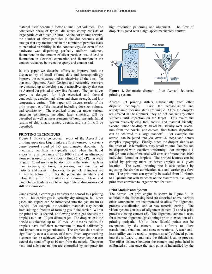
material itself become a factor at small dot volumes. The conductive phase of typical die attach epoxy consists of large particles of silver (>5 um). As the dot volume shrinks, the number of silver particles in the dot becomes small enough that any fluctuations in the number of particles leads to statistical variability in the conductivity. So even if the hardware was dispensing perfectly uniform volumes, fluctuations in the amount of silver particles would lead to fluctuation in electrical connection and fluctuation in the contact resistance between the epoxy and contact pad. In this paper we describe efforts to improve both the dispensability of small volume dots and correspondingly improve the consistency and conductivity of the dots. To that end, Optomec, Resin Designs and Assembly Answers have teamed up to develop a new nanosilver epoxy that can be Aerosol Jet printed to very fine features. The nanosilver epoxy is designed for high electrical and thermal conductivity, excellent adhesion and shear strength, and low temperature curing. This paper will discuss results of the print properties of the material including dot size, volume, and consistency. The electrical properties under various sintering conditions, including laser sintering, will be described as well as measurements of bond strength. Initial results of chip attach, printed circuits, and via fill will be described. PRINTING TECHNIQUES Figure 1 shows a conceptual layout of the Aerosol Jet printing apparatus. Liquid inks are first atomized to create a dense aerosol cloud of 1-5 µm diameter droplets. A pneumatic nebulizer is typically used when the liquid viscosity is in the range of 20-1000 cP and an ultrasonic atomizer is used for low viscosity fluids (1-20 cP). A wide range of liquid inks can be atomized in the system such as pure solvents, solutions, dispersions, and mixtures of particles and resins. However, the particle diameters are limited to below 1 µm for the pneumatic nebulizer and below 0.2 µm for the ultrasonic atomizer. Flake and nanotube particulates can have larger lateral dimensions and still be atomizable.
Once created, a carrier gas transfers the aerosol to a printing head. This carrier gas is typically dry nitrogen, but other gases and vapors can be introduced into the gas stream as needed. For example, air sensitive materials may benefit from adding a fraction of forming gas to the carrier. Within the print head, a second, co-flowing sheath gas focuses the droplets to a 10-100 µm diameter jet. The droplets exit the nozzle at velocities up to 100 m/s. At these velocities the droplets have sufficient momentum to travel ballistically and impact on a target substrate. The droplets do not slow significantly over a distance of 5 mm. Even larger working distances can be achieved with large diameter jets that can extend the standoff up to 10 mm from the nozzle. The print head and substrate motion are controlled by computer for
high resolution patterning and alignment. The flow of droplets is gated with a high-speed mechanical shutter.
Sheath Gas In
Focused BeamTo <10um
Dense Aerosol
2 to 5mm Standoff
Shea
th G
as In
Sheath Gas In
Focused BeamTo <10um
Dense Aerosol
2 to 5mm Standoff
Shea
th G
as In
Figure 1. Schematic diagram of an Aerosol Jet-based printing system.
Aerosol Jet printing differs substantially from other dispense techniques. First, the aerosolization and aerodynamic focusing steps are unique. Once the droplets are created in the atomizer, they do not contact any other surfaces until impaction on the target. This makes the system relatively clog free, robust, and material friendly. Second, since the droplets travel ballistically over several mm from the nozzle, non-contact, fine feature deposition can be achieved at a large standoff. For example, the aerosol can be jetted into via, over 3D steps, and across complex topography. Finally, since the droplet size is on the order of 10 femtoliters, very small volume features can be dispensed with excellent uniformity. For example a 1 mil (25 um) cube of material will consist of more than 1000 individual femtoliter droplets. The printed features can be scaled by printing more or fewer droplets at a given location. The overall printing rate is also scalable by adjusting the droplet atomization rate and carrier gas flow rate. The print rates can typically be scaled from 10 nl/min to 10 l/min but with tradeoffs on the feature size, i.e. larger print rates correlate to larger printed features. Print Module and System The Aerosol Jet print engine is shown in Figure 2. In addition to the dispensing head (6) described above, various other components are incorporated to allow for alignment, process visualization, and in situ material curing. The vision system consists of alignment camera (1) and a print process viewing camera (5). The alignment camera is used for substrate alignment (positioning) prior to execution of a printing toolpath. Up to three fiducial points can be recognized by the camera and software to allow translational, rotational, and skew corrections. A teach-and-learn utility can be used to program specific fiducial points into the software to automate the fiducial locating process. The offset distance between the camera and print head is calibrated so that once the start point is indentified by the
As originally published in the SMTA Proceedings.
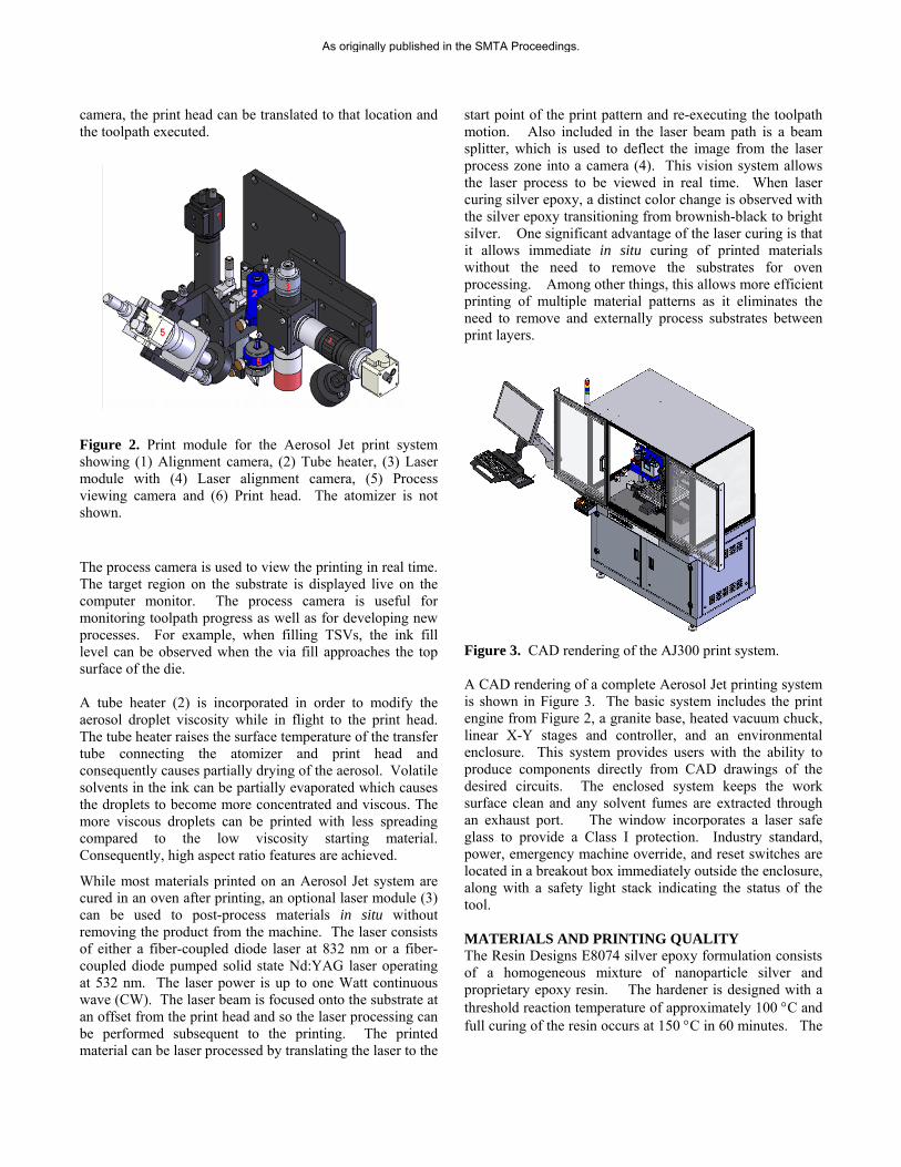
camera, the print head can be translated to that location and the toolpath executed.
Figure 2. Print module for the Aerosol Jet print system showing (1) Alignment camera, (2) Tube heater, (3) Laser module with (4) Laser alignment camera, (5) Process viewing camera and (6) Print head. The atomizer is not shown.
The process camera is used to view the printing in real time. The target region on the substrate is displayed live on the computer monitor. The process camera is useful for monitoring toolpath progress as well as for developing new processes. For example, when filling TSVs, the ink fill level can be observed when the via fill approaches the top surface of the die. A tube heater (2) is incorporated in order to modify the aerosol droplet viscosity while in flight to the print head. The tube heater raises the surface temperature of the transfer tube connecting the atomizer and print head and consequently causes partially drying of the aerosol. Volatile solvents in the ink can be partially evaporated which causes the droplets to become more concentrated and viscous. The more viscous droplets can be printed with less spreading compared to the low viscosity starting material. Consequently, high aspect ratio features are achieved.
While most materials printed on an Aerosol Jet system are cured in an oven after printing, an optional laser module (3) can be used to post-process materials in situ without removing the product from the machine. The laser consists of either a fiber-coupled diode laser at 832 nm or a fiber-coupled diode pumped solid state Nd:YAG laser operating at 532 nm. The laser power is up to one Watt continuous wave (CW). The laser beam is focused onto the substrate at an offset from the print head and so the laser processing can be performed subsequent to the printing. The printed material can be laser processed by translating the laser to the
start point of the print pattern and re-executing the toolpath motion. Also included in the laser beam path is a beam splitter, which is used to deflect the image from the laser process zone into a camera (4). This vision system allows the laser process to be viewed in real time. When laser curing silver epoxy, a distinct color change is observed with the silver epoxy transitioning from brownish-black to bright silver. One significant advantage of the laser curing is that it allows immediate in situ curing of printed materials without the need to remove the substrates for oven processing. Among other things, this allows more efficient printing of multiple material patterns as it eliminates the need to remove and externally process substrates between print layers.
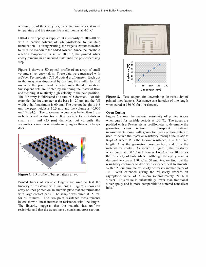
Figure 3. CAD rendering of the AJ300 print system. A CAD rendering of a complete Aerosol Jet printing system is shown in Figure 3. The basic system includes the print engine from Figure 2, a granite base, heated vacuum chuck, linear X-Y stages and controller, and an environmental enclosure. This system provides users with the ability to produce components directly from CAD drawings of the desired circuits. The enclosed system keeps the work surface clean and any solvent fumes are extracted through an exhaust port. The window incorporates a laser safe glass to provide a Class I protection. Industry standard, power, emergency machine override, and reset switches are located in a breakout box immediately outside the enclosure, along with a safety light stack indicating the status of the tool. MATERIALS AND PRINTING QUALITY The Resin Designs E8074 silver epoxy formulation consists of a homogeneous mixture of nanoparticle silver and proprietary epoxy resin. The hardener is designed with a threshold reaction temperature of approximately 100 C and full curing of the resin occurs at 150 C in 60 minutes. The
As originally published in the SMTA Proceedings.
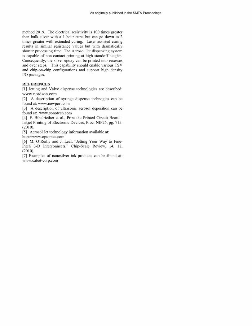
working life of the epoxy is greater than one week at room temperature and the storage life is six months at -10 C. E8074 silver epoxy is supplied at a viscosity of 100-200 cP with a carrier solvent of γ-butyrolactone to facilitate nebulization. During printing, the target substrate is heated to 60 C to evaporate the added solvent. Since the threshold reaction temperature is set at 100 C, the printed silver epoxy remains in an uncured state until the post-processing step. Figure 4 shows a 3D optical profile of an array of small volume, silver epoxy dots. These data were measured with a Cyber Technologies CT100 optical profilometer. Each dot in the array was dispensed by opening the shutter for 100 ms with the print head centered over the dot location. Subsequent dots are printed by shuttering the material flow and stepping at relatively high velocity to the next position. The 2D array is fabricated at a rate of 5 dots/sec. For this example, the dot diameter at the base is 120 um and the full width at half maximum is 60 um. The average height is 6.8 um, the peak height is 10.3 um, and the volume is 40,000 um3 (40 pL). The placement accuracy is better than 1 um in both x- and y- directions. It is possible to print dots as small as 1 mil (25 m) diameter, but currently the volumetric variation is significantly higher than with larger dots.
Figure 4. 3D profile of bump pattern array. Printed traces of variable lengths are used to test the linearity of resistance with line length. Figure 5 shows an array of lines printed on an alumina plate that are terminated with large contact pads. The sample was cured at 150 C for 60 minutes. The two point resistance measurements below show a linear increase in resistance with line length. The linearity suggests that the material has uniform resistivity and that the traces have a consistent cross section.
Figure 5. Test coupon for determining dc resistivity of printed lines (upper). Resistance as a function of line length when cured at 150 C for 1 hr (lower).
Oven Curing Figure 6 shows the material resistivity of printed traces when cured for variable periods at 150 C. The traces are profiled with a Dektak stylus profilometer to determine the geometric cross section. Four-point resistance measurements along with geometric cross section data are used to derive the material resistivity through the relation: R=L/A where R is the 4-point resistance, L is the trace length, A is the geometric cross section, and is the material resistivity. As shown in Figure 6, the resistivity when cured at 150 C in 1 hour is 1.6 -m or 100 times the resistivity of bulk silver. Although the epoxy resin is designed to cure at 150 C in 60 minutes, we find that the resisitivity continues to drop with extended heat treatments. With a 2 hour cure the resistivity decreases another factor of 10. With extended curing the resistivity reaches an asymptotic value of 3-cm (approximately 2x bulk silver). This value is substantially lower than traditional silver epoxy and is more comparable to sintered nanosilver inks.7
As originally published in the SMTA Proceedings.

Figure 6: Resistivity as a function of cure time at 150 C. Resistivity continues to decrease over several hours approaching an asymptotic value 2x of bulk silver. SEM analysis shows that after an initial cure the silver flakes sinter and form an interconnected metallic network. Figure 7 shows cross section SEM micrographs of uncured and cured silver epoxy. The uncured micrograph shows distinct, overlapping silver flakes. However, the micrograph of cured material clearly shows that the flakes are merging to form a connected metallic network. Consequently the increased conductivity observed with longer cure times may be a result of continued merging and densification of the silver flake. The high silver content in the epoxy then suggests that the primary conduction occurs through the metal network rather than by tunneling from particle to particle.
Figure 7. Cross section SEM of uncured silver epoxy (left) and silver epoxy cured for 2 hrs at 150 C (right). The individual plates merge over extended cure times. Laser Curing Since extended curing schedules may not be acceptable for some applications, we have also examined laser assisted curing. Figure 8 show a schematic of the laser curing technique used in the Optomec system as well as resistivity data. As mentioned above, the focused CW laser beam acts as a point source of heat to rapidly cure material under the impinging spot. In this case, a 200 mW, 832 nm laser is focused to a spot size of 20 m to give a peak intensity of 2x10⁵ W/cm2. The laser spot is scanned at a rate of 10 mm/s. Based on color changes observed while scanning the laser over a silver epoxy film, the heat affected zone is estimated to extend to 50 m. In other words, even though
the laser is focused to 20 m, the lateral heat spread is sufficient to process a 50 m spot. Printed features larger than 50 m can be cured by scanning the laser in a raster pattern with a 50 m pitch. A larger pitch and larger spot size would be possible with a more powerful laser.
Figure 8. Schematic diagram of laser sintering configuration (left). Resistivity of laser sintered silver epoxy compared to oven cured epoxy (right). While similar resistivity values are obtained, the laser process greatly reduces the overall cure time and can be performed without removing the substrate from the system for oven processing. The resistivity data in Figure 8 compares the resistivity of laser cured silver epoxy to the resistivity of epoxy that was cured in an oven at 150 C for 12 hrs. The values are similar to within 30%. The advantage of the laser cure process is that high conductivity can be achieved within minutes of printing the ink, whereas the oven curing requires hours for the lowest values. The laser curing can also be performed without removing the substrate from the system, so it can reduce the number of steps required for printing multiple layers of dissimilar materials. On the other hand, the laser requires a line of sight to the substrate, which is not always possible, especially if the epoxy is used to bond between a chip and PCB. Adhesive Properties One of the primary applications for dispensing nanosilver epoxy is for attaching chips to PCBs. Figure 9 shows images of 15 mil (375 µm) Kovar tabs attached to gold coated alumina. The epoxy pads are printed with a 20 mil (500 m) width and 1 mil (25 m) thickness. When the tabs are placed, the epoxy clearly wets the vertical edge and forms a fillet. Die shear measurements indicate that the highest shear strength is obtained when the epoxy wets the sidewall in this way. The measured die shear strength is 2000 PSI which is comparable to standard die attach epoxies and meets the MIL-STD-883, method 2019 minimum requirement of 882 PSI. Cohesive failure is seen in all cases. The glass transition temperature is approximately 100°C.
As originally published in the SMTA Proceedings.

Figure 9. 15 mil (375 µm) Kovar tab bonded to gold coated alumina substrate using silver epoxy. Applications Multiple bond pads can be printed at high density for attaching multiple I/O chips. Figure 10 shows the attachment of 0402 SMT resistors to ceramic substrate and QFN devices to glass plates. As described above, the substrates are heated to 60 C when jetting the silver epoxy pads. This temperature is sufficient to evaporate residual solvents in the epoxy, but low enough that the epoxy does not cure. The printed epoxy remains uncured until subjected to elevated temperatures of 100 C or higher. Consequently, it is possible to print a large number of bond pads sequentially and then attached the chips later. The chips shown in Figure 10 were manually placed with assistance of an optical microscope. The QFN sample also shows that the chips are physically connected to printed conductor lines.
Figure 10. Images of attached SMT devices using printed silver epoxy. The 0402 resistor (left) is attached to ceramic using 8 mil (200 m) pads with an 8 mil (m) gap between pads. The QFN chip (right) is attached to printed silver lines on glass substrate. Dots of epoxy have been printed on the ends of the lines and then the chip was placed manually with the assistance of a microscope. Compared to conventional nanoparticle silver inks, the silver epoxy exhibits far less shrinkage during curing. After solvent evaporation, the measured volumetric shrinkage during curing is less than 2.5%. Consequently, the silver epoxy may be more effective at producing solid conductive fills in confined geometries. One application where low shrinkage is required is in producing conductive via plugs in Through Silicon Via (TSV) die. Figure 11 shows an SEM cross section of a 50 m diameter by 300 m tall TSV, which contains jetted and cured silver epoxy. The fill process consists of several steps. The silver epoxy can be
jetted into an open via, but there is substantial leakage from the bottom side. Consequently, the amount of time required to fill the open via becomes variable, depending on the amount of leakage. In this work, an adhesive tape is applied to the back side of the die to convert from an open via to a blind geometry. The next step is to fill the via completely by dispensing liquid, silver epoxy down the center of the via. The epoxy flows to the bottom of the via and fills from the bottom upward. When full, the liquid epoxy is flush with the top surface. The platen is heated to 60 C to evaporate the solvent and in this drying process the top level of the epoxy recesses into the via. If needed, the filling step is repeated at least once more to return the liquid level to the top surface. Repeated partial fills can bring the dried epoxy level flush to the surface, but at the expense of additional process time. After filling and allowing the solvents to evaporate, the samples are fully cured at 150 C. Since the dried epoxy has low shrinkage, highly dense metal plugs are achieved.
Figure 11. SEM cross section of silicon via filled with silver epoxy. The cured silver epoxy appears bright white and a sidewall coating of plated copper is also evident. FUTURE WORK Future development work is planned for measuring thermal conductivity of the silver epoxy. High thermal conductivity is important for attaching power devices and heat generating chips. Given the high metal loading, the silver epoxy is expected to have an excellent thermal conductivity. Additional work is needed to determine contact resistance between the silver epoxy and various chip and board metallizations. Finally, a full characterization die shear strength as a function of bond line thickness is under way. CONCLUSIONS A new nanoflake silver epoxy has been developed for small feature, die attach applications. Using the Aerosol Jet tool, uniform dot sizes as small as 1 mil (25 m) can be dispensed. The epoxy is curable at 150 C and at that temperature the die shear strength exceeds MIL-STD-883,
As originally published in the SMTA Proceedings.
method 2019. The electrical resistivity is 100 times greater than bulk silver with a 1 hour cure, but can go down to 2 times greater with extended curing. Laser assisted curing results in similar resistance values but with dramatically shorter processing time. The Aerosol Jet dispensing system is capable of non-contact printing at high standoff heights. Consequently, the silver epoxy can be printed into recesses and over steps. This capability should enable various TSV and chip-on-chip configurations and support high density I/O packages. REFERENCES [1] Jetting and Valve dispense technologies are described: www.nordson.com [2] A description of syringe dispense technogies can be found at: www.newport.com [3] A description of ultrasonic aerosol deposition can be found at: www.sonotech.com [4] F. Bibelriether et al., Print the Printed Circuit Board - Inkjet Printing of Electronic Devices, Proc. NIP26, pg. 715. (2010). [5] Aerosol Jet technology information available at: http://www.optomec.com [6] M. O’Reilly and J. Leal, “Jetting Your Way to Fine-Pitch 3-D Interconnects,” Chip-Scale Review, 14, 18, (2010). [7] Examples of nanosilver ink products can be found at: www.cabot-corp.com
As originally published in the SMTA Proceedings.