adzs-21569-ezkit manual
TRANSCRIPT

ADZS-21569-EZKIT Manual
Revision 1.0, August 2019
Part Number82-000965-01
Analog Devices, Inc.One Technology WayNorwood, MA 02062-9106

Copyright Information
© 2019 Analog Devices, Inc., ALL RIGHTS RESERVED. This document may not be reproduced in any formwithout prior, express written consent from Analog Devices, Inc.
Disclaimer
Analog Devices, Inc. reserves the right to change this product without prior notice. Information furnished by Ana-log Devices is believed to be accurate and reliable. However, no responsibility is assumed by Analog Devices for itsuse; nor for any infringement of patents or other rights of third parties which may result from its use. No license isgranted by implication or otherwise under the patent rights of Analog Devices, Inc.
Trademark and Service Mark Notice
All other brand and product names are trademarks or service marks of their respective owners.
Regulatory Compliance
The ADZS-21569-EZKIT evaluation board is designed to be used solely in a laboratory environment. The board isnot intended for use as a consumer-end product or as a portion of a consumer-end product. The board is an opensystem design, which does not include a shielded enclosure and, therefore, may cause interference to other electricaldevices in close proximity. This board should not be used in or near any medical equipment or RF devices.
The ADZS-21569-EZKIT evaluation board is in the process of being certified to comply with the essential require-ments of the European EMC directive 2004/108/EC and, therefore, carries the “CE” mark.
ADZS-21569-EZKIT Manual ii

The ADZS-21569-EZKIT evaluation board contains ESD (electrostatic discharge) sensitive devices. Electrostaticcharges readily accumulate on the human body and equipment and can discharge without detection. Permanentdamage may occur on devices subjected to high-energy discharges. Proper ESD precautions are recommended toavoid performance degradation or loss of functionality. Store unused boards in the protective shipping package.
ADZS-21569-EZKIT Manual iii

Contents
Preface
Purpose of This Manual................................................................................................................................. 1–1
Manual Contents ........................................................................................................................................... 1–1
Technical Support .......................................................................................................................................... 1–1
Supported Integrated Circuit ......................................................................................................................... 1–1
Supported Tools............................................................................................................................................. 1–2
Product Information...................................................................................................................................... 1–2
Analog Devices Website.............................................................................................................................. 1–2
EngineerZone ............................................................................................................................................. 1–2
Using the Board
Product Overview .......................................................................................................................................... 2–1
Package Contents........................................................................................................................................... 2–3
Default Configuration ................................................................................................................................... 2–3
Debug Interface ............................................................................................................................................. 2–4
Power-On-Self Test........................................................................................................................................ 2–4
Example Programs ......................................................................................................................................... 2–4
Reference Design Information ....................................................................................................................... 2–4
Expansion Interface 3 .................................................................................................................................... 2–4
25LC010AT - 1K SPI Serial EEPROM ......................................................................................................... 2–5
AD2428 - Automotive Audio Bus A2B Transceiver ........................................................................................ 2–5
ADAU1962A - 12 Channel, High Performance, 192kHz, 24-Bit DAC ......................................................... 2–5
ADAU1977 - Quad ADC with Diagnostics ................................................................................................... 2–6
ADAU1979 - Quad Analog-to-Digital Converter .......................................................................................... 2–6
FT232R - USB to UART............................................................................................................................... 2–6
INA3221 - Triple Channel, High Measurement, Shunt and Bus Voltage Monitor ......................................... 2–7
IS25LP512M - 512M-bit Serial Flash Memory with Dual and Quad SPI ..................................................... 2–7
iv ADZS-21569-EZKIT Manual

MX66LM1G45G - 1G-bit Serial Flash Memory with Single and Octal SPI .................................................. 2–8
Hardware Reference
System Architecture ....................................................................................................................................... 3–1
Software-Controlled Switches (SoftConfig).................................................................................................... 3–2
Overview of SoftConfig .............................................................................................................................. 3–3
SoftConfig on the Board............................................................................................................................. 3–6
Programming SoftConfig Switches ............................................................................................................. 3–6
Switches....................................................................................................................................................... 3–10
Boot Mode Select ( SW1 ) ......................................................................................................................... 3–10
Reset Pushbutton ( SW2 ) ......................................................................................................................... 3–11
GPIO Pushbuttons ( SW4 and SW3 ) .................................................................................................. 3–11
Rotary Encoder ( SW7 ) ............................................................................................................................ 3–11
JTAG Interface ( SW5 and SW6 ) .......................................................................................................... 3–11
Jumpers ....................................................................................................................................................... 3–12
S/PDIF Loopback ( JP8 ) ........................................................................................................................ 3–13
Current Measurement ( P17, P18, P19, P20, and P21 ).......................................................... 3–13
HADC ( P1 ) ........................................................................................................................................... 3–13
LEDs ........................................................................................................................................................... 3–13
Fault ( LED4 ) .......................................................................................................................................... 3–14
USB to UART Activity ( LED5-6 ).......................................................................................................... 3–14
A2B Interrupt ( LED1 ) ............................................................................................................................ 3–14
Power ( LED8 ) ........................................................................................................................................ 3–14
GPIO ( LED7, LED10, LED9 ) .......................................................................................................... 3–14
Reset ( LED11 ) ....................................................................................................................................... 3–15
Connectors .................................................................................................................................................. 3–15
S/PDIF Optical Tx ( J1 )......................................................................................................................... 3–15
Clock ( J2 ).............................................................................................................................................. 3–16
Audio Input/Output ( J3 )....................................................................................................................... 3–16
Link Port/JTAG ( J8 and J9 ) ............................................................................................................. 3–16
ADZS-21569-EZKIT Manual v

S/PDIF Optical Rx ( J11 ) ...................................................................................................................... 3–16
Audio Output ( J10 ) .............................................................................................................................. 3–16
S/PDIF Digital ( J11 ) ............................................................................................................................ 3–16
MLB ( J12 ) ............................................................................................................................................ 3–17
Headphone ( J13 ) .................................................................................................................................. 3–17
HADC ( P1 and J4 ) ........................................................................................................................... 3–17
JTAG ( P4 ).............................................................................................................................................. 3–17
Sigma Studio ( P5 ) .................................................................................................................................. 3–17
Trace and JTAG ( P8 ).............................................................................................................................. 3–17
USB to UART( P11 )............................................................................................................................... 3–18
A2B ( P10 and P11 ) ........................................................................................................................... 3–18
Engine RPM ( P12 ) ................................................................................................................................ 3–18
Microphone ( P13-P16 ) ........................................................................................................................ 3–18
Power Plug ( P10 )................................................................................................................................... 3–18
Power Terminal Block ( P22 ) .................................................................................................................. 3–19
Expansion Interface 3 ( P9 and P7 ) .................................................................................................... 3–19
vi ADZS-21569-EZKIT Manual

1 Preface
Thank you for purchasing the Analog Devices, Inc. ADZS-21569-EZKIT evaluation system.
Purpose of This ManualThis manual provides instructions for installing the product hardware (board). This manual describes operation andconfiguration of the board components and provides guidelines for running code on the board.
Manual ContentsThe manual consists of:
• Using the board
Provides basic board information.
• Hardware Reference
Provides information about the hardware aspects of the board.
• Bill of Materials
A companion file in PDF format that lists all of the components used on the board is available on the websiteat http://www.analog.com/ADZS-21569-EZKIT .
• Schematic
A companion file in PDF format documenting all of the circuits used on the board is available on the websiteat http://www.analog.com/ADZS-21569-EZKIT .
Technical Support
Supported Integrated CircuitThis evaluation system supports the Analog Devices ADSP-21569 IC.
Preface
ADZS-21569-EZKIT Manual 1–1

Supported Tools
Product Information
Analog Devices Website
The Analog Devices website, http://www.analog.com, provides information about a broad range of products - ana-log integrated circuits, amplifiers, converters, transceivers, and digital signal processors.
Also note, MyAnalog.com is a free feature of the Analog Devices website that allows customization of a web page todisplay only the latest information about products you are interested in. You can choose to receive weekly e-mailnotifications containing updates to the web pages that meet your interests, including documentation errata againstall manuals. MyAnalog.com provides access to books, application notes, data sheets, code examples, and more.
Visit MyAnalog.com to sign up. If you are a registered user, just log on. Your user name is your e-mail address.
EngineerZone
EngineerZone is a technical support forum from Analog Devices, Inc. It allows you direct access to ADI technicalsupport engineers. You can search FAQs and technical information to get quick answers to your embedded process-ing and DSP design questions.
Use EngineerZone to connect with other DSP developers who face similar design challenges. You can also use thisopen forum to share knowledge and collaborate with the ADI support team and your peers. Visit http://ez.analog.com to sign up.
Supported Tools
1–2 ADZS-21569-EZKIT Manual

2 Using the Board
This chapter provides information on the major components and peripherals on the board, along with instructionsfor installing and setting up the emulation software.
Product OverviewThe board features:
• Analog Devices ADSP-21569 processor
• 400 ball BGA
• 25 MHz oscillator
• DDR3 Memory
• 512Mx16 bit (8Gbit )
• ISSI IS43TR16512BL-125KBL
• 1.35V
• SPI Flash Quad (SPI2) Memory
• 512Mbit
• ISSI IS25LP512M - 512M-bit Serial Flash Memory with Dual and Quad SPI
• Single/Dual/Quad SPI
• SPI Flash Octal (SPI2) Memory
• 1Gbit
• Macronix MX66LM1G45G - 1G-bit Serial Flash Memory with Single and Octal SPI
• Single/Octal SPI
• SPI EEPROM
• Microchip 25LC010AT - 1K SPI Serial EEPROM
• Audio
Using the Board
ADZS-21569-EZKIT Manual 2–1

• Analog Devices ADAU1962A - 12 Channel, High Performance, 192kHz, 24-Bit DAC
• Analog Devices ADAU1977 - Quad ADC with Diagnostics
• Analog Devices ADAU1979 - Quad Analog-to-Digital Converter
• 12 RCA connectors. 12 outputs or 8 outputs/4 inputs
• Universal Asynchronous Receiver/Transmitter (UART0)
• FTDI FT232R - USB to UART
• USB micro-B
• A2B
• Analog Devices AD2428 - Automotive Audio Bus A2B Transceiver
• Two DuraClik connectors
• Debug Interface (JTAG and Trace)
• ICE-1000 emulator
• JTAG 10-pin 0.05” header
• JTAG and Trace 38-pin Mictor connector
• LEDs
• 11 LEDs: one power (green), one board reset (red), 3 general-purpose (amber), 3 A2B LEDs, one fault(red) and 2 UART leds (amber)
• Pushbuttons
• Three pushbuttons: one reset and two IRQ/Flag
• EI3 connector
• SMC
• EPPI
• SPORT
• SPI
• UART
• TWI
• TMR
• GPIO
• RESET
Product Overview
2–2 ADZS-21569-EZKIT Manual

• GND/3.3V/5V output
• External power supply
• CE compliant
• 12V @1.6 Amps
• Power measurement
• 0.051-ohm resistors for measuring current draw
Package ContentsYour ADZS-21569-EZKIT package contains the following items.
• ADZS-21569-EZKIT board
• Universal 12V DC power supply
• USB 2.0 type A to micro-B cable
• ICE-1000 emulator
Contact the vendor where you purchased your ADZS-21569-EZKIT evaluation board or contact Analog Devices,Inc. if any item is missing.
Default ConfigurationThe ADZS-21569-EZKIT board is designed to run as a standalone unit.
The Default Hardware Setup figure shows the default settings for jumpers and switches and the location of thejumpers, switches, connectors, and LEDs. Confirm that your board is in the default configuration before using theboard.
Default Config
Figure 2-1: Default Hardware Setup
NOTE: Connectors on the back of the board are noted with dotted lines if applicable.
Package Contents
ADZS-21569-EZKIT Manual 2–3

Debug InterfaceThe ADZS-21569-EZKIT provides a JTAG and Trace connection via P4 or P8.
Power-On-Self TestThe Power-On-Self-Test Program (POST) tests all EZ-KIT peripherals and validates functionality as well as connec-tivity to the processor. Once assembled, each EZ-KIT is fully tested for an extended period of time with POST. AllEZ-KIT boards are shipped with POST preloaded into flash memory. The POST is executed by resetting the boardand connecting the USB To UART to your PC and open up a terminal window. The POST also can be used as areference for a custom software design or hardware troubleshooting.
Note that the source code for the POST program is included in the Board Support Package (BSP) along with thereadme file that describes how the board is configured to run POST.
Example ProgramsExample programs are provided with the ADZS-21569-EZKIT Board Support Package (BSP) to demonstrate vari-ous capabilities of the product. The programs can be found in the ADSP-21569_EZ-KIT\examples installa-tion folder. Refer to the readme file provided with each example for more information.
Reference Design InformationA reference design info package is available for download on the Analog Devices Web site. The package providesinformation on the schematic design, layout, fabrication, and assembly of the board.
The information can be found at:
http://www.analog.com/ADZS-21569-EZKIT
Expansion Interface 3The Expansion Interface 3 (EI3) interface supports connecting with other EI3 daughterboards designed by AnalogDevices, extending the evaluation system's capabilities. The connectors provide power, ground, reset, ADC, PPI,TWI, UART, SPORT, SMC and GPIO signals.
The expansion interface is architected to provide support for modularity with different expansion board types. Thesetypes fall into several categories including audio, video, converter, and asynchronous memory.
More information about available extender boards can be found at: http://www.analog.com/en/design-center/land-ing-pages/001/sharc-processors-software-and-tools.html
Debug Interface
2–4 ADZS-21569-EZKIT Manual

25LC010AT - 1K SPI Serial EEPROMThe Microchip Technology Inc. 25XX010A* is a 1 Kbit Serial Electrically Erasable Programmable Read-Only Mem-ory (EEPROM). The memory is accessed via a simple Serial Peripheral Interface (SPI) compatible serial bus. Thebus signals required are a clock input (SCK) plus separate data in (SI) and data out (SO) lines. Access to the device iscontrolled through a Chip Select (CS) input.
AD2428 - Automotive Audio Bus A2B Transceiver
The Automotive Audio Bus (A2B®) provides a multichannel, I2S/TDM link over distances of up to 15 m betweennodes. It embeds bidirectional synchronous pulse-code modulation (PCM) data (for example, digital audio), clock,
and synchronization signals onto a single differential wire pair. A2B supports a direct point to point connection andallows multiple, daisy-chained nodes at different locations to contribute and/or consume time division multiplexedchannel content.
A2B is a single-master, multiple-slave system where the transceiver chip at the host controller is the master. The mas-
ter generates clock, synchronization, and framing for all slave nodes. The master A2B chip is programmable over a
control bus (I2C) for configuration and read back. An extension of this control bus is embedded in the A2B data
stream, which grants direct access of registers and status information on slave transceivers as well as I2C to I2C com-munication over distance.
The transceiver can connect directly to general-purpose digital signal processors (DSPs), field-programmable gatearrays (FPGAs), application specific integrated circuits (ASICs), microphones, analog-to-digital converters (ADCs),
digital-toanalog converters (DACs), and codecs through a multichannel I2S/TDM interface. It also provides a pulsedensity modulation (PDM) interface for direct connection of up to four PDM digital microphones.
Finally, the transceiver also supports an A2B bus powering feature, where the master node supplies voltage and cur-rent to the slave nodes over the same daisy-chained, twisted pair wire cable as used for the communication link.
ADAU1962A - 12 Channel, High Performance, 192kHz, 24-BitDACThe ADAU1962A is a high performance, single-chip digital-to-analog converter (DAC) that provides 12 DACswith differential or single-ended output using the Analog Devices, Inc., patented multibit sigma-delta (Σ-Δ) archi-tecture. A serial peripheral interface (SPI)/I2C port is included, allowing a micro-controller to adjust volume andmany other parameters. The ADAU1962A operates from 2.5 V digital and 3.3 V analog supplies. A linear regulatoris included to generate the digital supply voltage from the analog supply voltage.
The ADAU1962A is designed for low EMI. This consideration is apparent in both the system and circuit designarchitectures. By using the on-board PLL to derive the internal master clock from an external LRCLK, theADAU1962A can eliminate the need for a separate high frequency master clock and can be used with or without a
25LC010AT - 1K SPI Serial EEPROM
ADZS-21569-EZKIT Manual 2–5

bit clock. The DACs are designed using the latest Analog Devices continuous time architectures to further minimizeEMI.
ADAU1977 - Quad ADC with DiagnosticsThe ADAU1977 incorporates four high performance analog-todigital converters (ADCs) with direct-coupled inputscapable of 10 V rms. The ADC uses multibit sigma-delta (Σ-Δ) architecture with continuous time front end for lowEMI. The ADCs can be connected to the electret microphone (ECM) directly and provide the bias for powering themicrophone. Built-in diagnostic circuitry detects faults on input lines and includes comprehensive diagnostics forfaults on microphone inputs. The faults reported are short to battery, short to microphone bias, short to ground,short between positive and negative input pins, and open input terminals. In addition, each diagnostic fault is availa-ble as an IRQ flag for ease in system design. An I2C/SPI control port is also included. The ADAU1977 uses only asingle 3.3 V supply. The part internally generates the microphone bias voltage. The microphone bias is programma-ble in a few steps from 5 V to 9 V. The low power architecture reduces the power consumption. An on-chip PLLcan derive the master clock from an external clock input or frame clock (sample rate clock). When fed with a frameclock, the PLL eliminates the need for a separate high frequency master clock in the system.
ADAU1979 - Quad Analog-to-Digital ConverterThe ADAU1979 incorporates four high performance, analog-to-digital converters (ADCs) with 4.5 V rms capableac-coupled inputs. The ADCs use a multibit sigma-delta (Σ-Δ) architecture with continuous time front end for lowEMI. An I2C/serial peripheral interface (SPI) control port is included that allows a microcontroller to adjust volumeand many other parameters. The ADAU1979 uses only a single 3.3 V supply. The device internally generates therequired digital DVDD supply. The low power architecture reduces the power consumption. The on-chip PLL canderive the master clock from an external clock input or frame clock (sample rate clock). When fed with the frameclock, it eliminates the need for a separate high frequency master clock in the system.
FT232R - USB to UARTThe FT232R is a USB-to-serial-UART interface with the following advanced features:
• Single chip USB to asynchronous serial data transfer interface
• Entire USB protocol handled on the chip. No USB specific firmware programming required
• Fully-integrated 1024 bit EEPROM storing device descriptors and CBUS I/O configuration
• Fully-integrated USB termination resistors
• Fully-integrated clock generation with no external crystal required, plus optional clock output selection ena-bling a glue-less interface to external MCU or FPGA
• Data transfer rates from 300 baud to 3 Mbaud (RS422, RS485, RS232) at TTL levels
• 128 byte receive buffer and 256 byte transmit buffer utilizing buffer smoothing technology to allow for high-data throughput
ADAU1977 - Quad ADC with Diagnostics
2–6 ADZS-21569-EZKIT Manual

• FTDI’s royalty-free Virtual Com Port (VCP) and Direct (D2XX) drivers eliminate the requirement for USBdriver development in most cases.
• Transmit and receive LED drive signals
• UART interface support for 7 or 8 data bits, 1 or 2 stop bits and odd / even / mark / space / no parity
• FIFO receives and transmits buffers for high-data throughput
• Device supplied pre-programmed with unique USB serial number
• Supports bus powered, self-powered and high-power bus powered USB configurations
• Integrated +3.3V level converter for USB I/O
• Integrated level converter on UART and CBUS for interfacing to between +1.8V and +5V logic
• True 5V/3.3V/2.8V/1.8V CMOS drive output and TTL input
• Configurable I/O pin output drive strength
• Integrated power-on-reset circuit
• Fully-integrated AVCC supply filtering - no external filtering required.
• UART signal inversion option
• +3.3V (using external oscillator) to +5.25V (internal oscillator) single supply operation
• Low-operating and USB suspend current
• Low USB bandwidth consumption
• UHCI/OHCI/EHCI host controller compatible
• USB 2.0 full speed compatible
INA3221 - Triple Channel, High Measurement, Shunt and BusVoltage MonitorThe INA3221 is a three-channel, high-side current and bus voltage monitor with an I2C- and SMBUS-compatibleinterface. The INA3221 monitors both shunt voltage drops and bus supply voltages, in addition to having program-mable conversion times and averaging modes for these signals. The INA3221 offers both critical and warning alertsto detect multiple programmable out-of-range conditions for each channel.
IS25LP512M - 512M-bit Serial Flash Memory with Dual andQuad SPIThe IS25LP512M and IS25WP512M Serial Flash memory offers a versatile storage solution with high flexibilityand performance in a simplified pin count package. ISSI’s “Industry Standard Serial Interface” Flash is for systems
INA3221 - Triple Channel, High Measurement, Shunt and Bus Voltage Monitor
ADZS-21569-EZKIT Manual 2–7

that require limited space, a low pin count, and low power consumption. The device is accessed through a 4-wireSPI Interface consisting of a Serial Data Input (SI), Serial Data Output (SO), Serial Clock (SCK), and Chip Enable(CE#) pins, which can also be configured to serve as multi-I/O (see pin descriptions).
The device supports Dual and Quad I/O as well as standard, Dual Output, and Quad Output SPI. Clock frequen-cies of up to 133MHz allow for equivalent clock rates of up to 532MHz (133MHz x 4) which equates to66.5Mbytes/sof data throughput. The IS25xE series of Flash adds support for DTR (Double Transfer Rate) com-mands that transfer addressesand read data on both edges of the clock.These transfer rates can outperform 16-bitParallel Flash memories allowing for efficient memory access to support XIP (eXecute In Place) operation.
The memory array is organized into programmable pages of 256/512bytes. This family supports page programmode where 1 to 256/512bytes of data areprogrammed in a single command.
QPI (Quad Peripheral Interface) supports 2-cycle instruction further reducing instruction times. Pages can be erasedin groups of 4Kbyte sectors, 32Kbyte blocks, 64K/256Kbyte blocks, and/or the entire chip. The uniform sector andblock architecture allows for a high degree of flexibility so that the device can be utilized for a broad variety of appli-cations requiring solid data retention.
MX66LM1G45G - 1G-bit Serial Flash Memory with Single andOctal SPIMX66LM1G45G is 1Gbit Serial NOR Flash memory, which is configured as 134,217,728 x 8 internally.MX66LM1G45G feature a serial peripheral interface and software protocol allowing operation on a simple 3-wirebus while it is in single I/O mode. The three bus signals are a clock input (SCLK), a serial data input (SI), and aserial data output (SO). Serial access to the device is enabled by CS# input.
The MX66LM1G45G MXSMIO® (Serial Multi I/O) provides sequential read operation on whole chip.
MX66LM1G45G - 1G-bit Serial Flash Memory with Single and Octal SPI
2–8 ADZS-21569-EZKIT Manual

3 Hardware Reference
This chapter describes the hardware design of the ADZS-21569-EZKIT .
System ArchitectureThe board's configuration is shown in the Block Diagram figure.
Hardware Reference
ADZS-21569-EZKIT Manual 3–1

ADSP-21569
JTAG
Po
rt
Power Regulation
12 RCA(4)ADC/(8)DAC
(12)DAC
Link
Po
rt 1
Link
Po
rt 0
DAI
CLK/TWI2
Link Port
FT232RQ
Mini A/B
SPDIFCIRC
SPDIF IN
SPDIF OUT
12VPWR IN Expansion
Interface3
(EI3)SMC
EPPI
GPIO
Link Port
DMCSPI2
UART0
ADC/DACADAU1979
ADAU1962A
MLB MLB
Conn
Programamble Oscillator
SPI TWI SPORT
JTAGTRACE
SMSCINIC Eval
Board
A2B
PBs/LEDs G
PIO
DAI/TWI2
SPI0
8.5V5.0V3.3V1.8V1.35V1.0V
UART
DAI
TWI22mm
(2)
1KEEPROM
SPI1
TWI2 USBi
Cou
nter
Thumbwheel
PowerRails
SMA(4)
HADC
Mic In(4)
ADCADAU1977
SPI2
SPIFlash1 Gb
MX66LM1G56G
SPI Flash
512MB IS25LP512M
8Gb DDR3
IS43TR16512BL-125JK
Figure 3-1: Block Diagram
This EZ-KIT is designed to demonstrate the ADSP-21569 processor’s capabilities. The board has a 25 MHz inputclock and runs at a max core clock frequency of 1GHz.
User I/O to the processor is provided in the form of two pushbuttons and three LEDs.
The software-controlled switches (SoftConfig) facilitate the switch multi-functionality by disconnecting the push-buttons from their associated processor pins and reusing the pins elsewhere on the board.
Software-Controlled Switches (SoftConfig)On the board, most of the traditional mechanical switches and jumpers have been replaced by I2C software-control-led switches. The remaining mechanical switches are provided for the boot mode and pushbuttons. Reference anySoftConfig*.c file found in the installation directory for an example of how to set up the SoftConfig feature of
Software-Controlled Switches (SoftConfig)
3–2 ADZS-21569-EZKIT Manual

the board through software. The SoftConfig section of this manual serves as a reference to any user that intends tomodify an existing software example. If software provided by ADI is used, there should be little need to referencethis section.
NOTE: Care should be taken when changing SoftConfig settings not to create a conflict with interfaces. This isespecially true when connecting extender cards.
Overview of SoftConfig
In order to further clarify the use of electronic single FET switches and multi-channel bus switches, an example ofeach is illustrated and compared to a traditional mechanical switching solution. This is a generic example that usessimilar FET and bus switch components that are on the board.
After this generic discussion there is a detailed explanation of the SoftConfig interface specific to the ADZS-21569-EZKIT .
The Example of Individual FET Switches figure shows two individual FET switches (Pericom PI3A125CEX) withreference designators UA and UB. Net names ENABLE_A and ENABLE_B control UA and UB. The default FETswitch enable settings in this example are controlled by resistors RA and RB which pull the enable pin 1 of UA andUB to ground (low). In a real example, these enable signals are controlled by the Microchip IO expander. The de-fault pull-down resistors connects the signals EXAMPLE_SIGNAL_A and EXAMPLE_SIGNAL_B and also con-nects signals EXAMPLE_SIGNAL_C and EXAMPLE_SIGNAL_D. To disconnect EXAMPLE_SIGNAL_A fromEXAMPLE_SIGNAL_B, the Microchip IO expander is used to change ENABLE_A to a logic 1 through softwarethat interfaces with the Microchip. The same procedure for ENABLE_B disconnects EXAMPLE_SIGNAL_C fromEXAMPLE_SIGNAL_D.
Figure 3-2: Example of Individual FET Switches
Software-Controlled Switches (SoftConfig)
ADZS-21569-EZKIT Manual 3–3

The following figure shows the equivalent circuit to the Example of Individual FET Switches figure but utilizes me-chanical switches that are in the same package. Notice the default is shown by black boxes located closer to the ONlabel of the switches. In order to disconnect these switches, physically move the switch to the OFF position.
Figure 3-3: Example of a Mechanical Switch (Equivalent to Example of Individual FET Switches Figure)
The Example of Bus Switch figure shows a bus switch example, reference designator UC (PericomPI3LVD512ZHE), selecting between lettered functionality and numbered functionality. The signals on the left sideare multiplexed signals with naming convention letter_number. The right side of the circuit shows the signals sepa-rated into letter and number, with the number on the lower group (0B1) and the letter on the upper group (0B2).The default setting is controlled by the signal CONTROL_LETTER_NUMBER which is pulled low. This selects thenumber signals on the right to be connected to the multiplexed signals on the left by default. In this example, theMicrochip IO expander is not shown but controls the signal CONTROL_LETTER_NUMBER and allows the user tochange the selection through software.
Software-Controlled Switches (SoftConfig)
3–4 ADZS-21569-EZKIT Manual
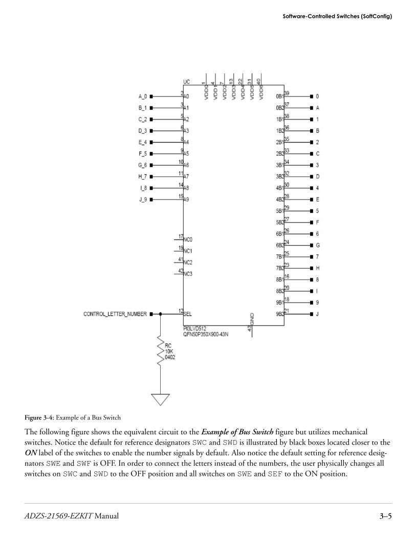
Figure 3-4: Example of a Bus Switch
The following figure shows the equivalent circuit to the Example of Bus Switch figure but utilizes mechanicalswitches. Notice the default for reference designators SWC and SWD is illustrated by black boxes located closer to theON label of the switches to enable the number signals by default. Also notice the default setting for reference desig-nators SWE and SWF is OFF. In order to connect the letters instead of the numbers, the user physically changes allswitches on SWC and SWD to the OFF position and all switches on SWE and SEF to the ON position.
Software-Controlled Switches (SoftConfig)
ADZS-21569-EZKIT Manual 3–5

Figure 3-5: Example of a Mechanical Switch (Equivalent to Example of Bus Switch)
SoftConfig on the Board
Two Microchip MCP23017 GPIO expanders provide control for individual electronic switches. The TWI2 inter-face of the processor communicates with the Microchip devices. There are individual switches with default settingsthat enable basic board functionality.
The Default Processor Interface Availability table lists the processor and board interfaces that are available by de-fault. Note that only interfaces affected by software switches are listed in the table.
Table 3-1: Default Processor Interface Availability
Interface Availability by Default
UART0 USB to UART FTDI232RQ
SPI Flash Quad mode enabled
Audio Connectors 4 inputs/8 outputs
S/PDIF Digital S/PDIF RCA input and output connectors enabled
Pushbuttons Enabled
LEDs Enabled
Programming SoftConfig Switches
On the board, two Microchip MCP23017 devices exist. Each of these devices have the following programmingcharacteristics:
• Each GPIO register controls eight signals (software switches).
Software-Controlled Switches (SoftConfig)
3–6 ADZS-21569-EZKIT Manual

GPIO Register Register Address
GPIOA 0x12
GPIOB 0x13
• By default, the Microchip MCP23017 GPIO signals function as input signals.
The signals must be programmed as output signals to override their default values. A zero is programmed intothe register to enable the signal as an output. The following table shows the Microchip register addresses.
IODIR Register IODIR Register Address
IODIRA 0x00
IODIRB 0x01
Each example in the Board Support Software (BSP) includes source files that program the soft switches, even if thedefault settings are being used. The README for each example identifies only the signals that are being changedfrom their default values. The code that programs the soft switches is located in the SoftConfig_XXX.c file ineach example where XXX is the name of the baord.
The following tables (I2C Hardware Address 0x21 and I2C Hardware Address 0x22) outline the default values foreach of the two Microchip MCP23017 devices.
Table 3-2: I2C Hardware Address 0x21
GPIO MCP23017 Register Address Default Value
GPIOA 0x12 0x02
GPIOB 0x13 0xC4
Table 3-3: I2C Hardware Address 0x22
GPIO MCP23017 Register Address Default Value
GPIOA 0x12 0xE0
GPIOB 0x13 0xFF
The board schematic shows how the two Microchip GPIO expanders are connected to the board’s ICs.
Tables Output Signals of Microchip GPIO Expander (U47 Port A) and Output Signals of Microchip GPIO Expand-er (U47 Port B) show the output signals of the Microchip GPIO expander (U47), with a TWI address of 0100001X, where X represents the read or write bit. The signals that control an individual FET have an entry in theFET column. The Component Connected column shows the board IC that is connected if the FET is enabled. TheMicrochip (U47) is controlling the enable signal of a FET switch. Also note that if a particular functionality of theprocessor signal is being used, it is in bold font in the Processor Signal column.
Software-Controlled Switches (SoftConfig)
ADZS-21569-EZKIT Manual 3–7

Table 3-4: Output Signals of Microchip GPIO Expander (U48 Port A)
Bit Signal Name Description FET Processor Signal
(if applicable)
Connected Default
0 EEPROM_EN SPI EEPROM CS U25 PA_09/SPI0_SEL1b/UART0_CTSb/OSPI_D7/SMC0_D09/SPI0_SSb
U41 High
1 UART0_FLOW_EN
UART0 Flow Control U32 PA_08/SPI0_MOSI/UART0_RTSb/OSPI_D6/SMC0_D08/TM0_ACLK2
U31 Low
2 UART0_EN Enables UART0 U32 PA_06/SPI0_CLK/UART0_TXb/OSPI_D4/SMC0_D06/TM0_ACLK1
U31 Low
3 ADAU_RESET Reset ADAU ICs U6, U7, U8 None U40, U43,U44
High
4 OCTAL_SPI_CS_EN
Connects Octal CS to SPI port U16 PA_05/SPI2_SEL1b/OSPI_SEL1b/SMC0_D05/SPI2_SSb
U47 High
5 OCTAL_SPI_CONNECT
Connects Octal signals to SPIport
U17 PA_00/SPI2_MISO/OSPI_MISO/SMC0_D00
U47 High
6 THUMBWHEEL_OE
Enables Rotary Switch U48 Counter signals U57 High
7 NOT USED
Table 3-5: Output Signals of Microchip GPIO Expander (U48 Port B)
Bit Signal Name Description FET Processor Signal
(if applicable)
Connected Default
0 ADAU1962_EN Enables ADAU1962 U7 DAI0_PIN02, DAI0_PIN04,DAI0_PIN0, DAI0_PIN05 andDAI0_PIN10
U40 High
1 ADAU1979_EN Enables ADAU1979 U7 DAI0_PIN20, DAI0_PIN12,DAI0_PIN06 and DAI0_PIN07
U43 High
2 AUDIO_JACK_SEL
Selects between connector beingconfigured for input or output
U40 None J3 High
3 NOT USED4 SPI2FLASH_
CS_ENSPI2 FLASH CS U26 PB_15/SPI2_SEL1b U30 Low
5 SPI2D2_D3_EN
Enables Quad mode for SPI2Flash
U27 andU28
PB_12/SPI2_D2 and PB_13/SPI2_D3
U30 Low
6 SPDIF_OPTICAL
Enables S/PDIF optical connec-tors
U10 andU13
DAI0_PIN09, DAI0_PIN10 J1 and J2 Low
Software-Controlled Switches (SoftConfig)
3–8 ADZS-21569-EZKIT Manual

Table 3-5: Output Signals of Microchip GPIO Expander (U48 Port B) (Continued)
Bit Signal Name Description FET Processor Signal
(if applicable)
Connected Default
7 SPDIF_DIGITAL_EN
Enables S/PDIF digital connec-tors
U11 andU12
DAI0_PIN09, DAI0_PIN10 J11 High
Tables Output Signals of Microchip GPIO Expander (U48 Port A) and Signals of Microchip GPIO Expander (U48Port B) show the output signals of the Microchip GPIO expander (U48), with a TWI address of 0100 010X,where X represents the read or write bit. The signals that control an individual FET have an entry in the FET col-umn. The Component Connected column shows the board IC that is connected if the FET is enabled. However, inmost cases, the Microchip (U48) is controlling the enable signal of a FET switch. Also note that if a particular func-tionality of the processor signal is being used, it is in bold font in the Processor Signal column.
Table 3-6: Output Signals of Microchip GPIO Expander (U48 Port A)
Bit Signal Name Description FET Processor Signal
(if applicable)
Connected Default
0 NOT USED1 PUSHBUTTON2
_ENPC_07 is used as GPIO inputfor push button 2, enabled bydefault
U15 PC_07/LP1_CLK/OSPI_SEL4b/TM0_TMR9/SYS_FAULT
SW3 Low
2 PUSHBUTTON1_EN
PB_03 is used as GPIO input forpush button 1, enabled by de-fault
U14 PB_03/TM0_TMR3/FLG2/SPI2_SEL2b/SMC0_ADDR1/CNT0_UD
SW4 Low
3 LEDS_EN Px & DAI is used as GPIO out-put for LED7,9,10 enabled bydefault
U8 DAI0_PINI08, DAI0_PIN11,PB_03
LED7,9,10 Low
4 NOT USED5 NOT USED6 NOT USED7 NOT USED
Table 3-7: Output Signals of Microchip GPIO Expander (U48 Port B)
Bit Signal Name Description FET Processor Signal
(if applicable)
Connected Default
0 ADAU1977_EN Enables ADAU1977 U8 DAI0_PIN08, DAI0_PIN09,DAI0_PIN11 and DAI0_PIN19
U44 High
1 ADAU1977_FAULT_RST_EN
Enables ADAU1977 FAULT andRESET
U7 PB_13/LP0_D6/SPI1_SEL3b/UART2_RTSb and ADAU_RE-SET
U44 High
Software-Controlled Switches (SoftConfig)
ADZS-21569-EZKIT Manual 3–9

Table 3-7: Output Signals of Microchip GPIO Expander (U48 Port B) (Continued)
Bit Signal Name Description FET Processor Signal
(if applicable)
Connected Default
2 NOT USED3 ENGINE_RPM_
OEPE_09 is used as an input for en-gine RPM, disabled by default
U52 PA_00/SMC0_A01 P12 High
4 NOT USED5 NOT USED6 NOT USED
7 NOT USED
SwitchesThis section describes operation of the switches. The switch locations are shown in the Switch Locations figure.
Figure 3-6: Switch Locations
Boot Mode Select ( SW1 )
The Boot Mode selection switch selects between the different boot modes of the processor. The Boot Mode Switchtable shows the available boot mode settings. By default, the processor boots from SPI2 master boot which uses theon-board SPI flash memory.
Table 3-8: Boot Mode Switch
Position Processor Boot Mode
0 No Boot
1 SPI Master Boot
2 SPI Slave Boot
3 UART Boot
4 Link Port Boot
Switches
3–10 ADZS-21569-EZKIT Manual

Table 3-8: Boot Mode Switch (Continued)
Position Processor Boot Mode
5 OSPI Master Boot
6 Reserved
7 Reserved
Reset Pushbutton ( SW2 )
The reset pushbutton resets the ADSP-21569 processor. The reset signal also is connected to the expansion connec-tors via the SYS_HWRSTsignal. Reset ( LED11 ) is used to indicate when the board is in reset.
GPIO Pushbuttons ( SW4 and SW3 )
The GPIO pushbuttons are connected to the processor’s signals PB_03/TM0_TMR3/FLG2/SPI2_SEL2b/SMC0_ADDR1/CNT0_UD and PC_07/LP1_CLK/OSPI_SEL4b/TM0_TMR9/SYS_FAULT , respectively.
The GPIO pushbuttons can be disconnected from the processor by setting SoftConfig, see Software-ControlledSwitches (SoftConfig) for more information.
Rotary Encoder ( SW7 )
The rotary encoder can be turned clockwise for an up count or counter-clockwise for a down count. The encoderalso features a momentary switch, activated by pushing the switch towards the center of the board, that can be usedto set the counter to zero. The rotary encoder is a two-bit quadrature (Gray code) encoder.
The rotary encoder can be disconnected from the processor by setting SoftConfig, see Software-Controlled Switches(SoftConfig) for more information.
JTAG Interface ( SW5 and SW6 )
The JTAG Interface switches select between a single processor (one board) and multiprocessor (more than oneboard) configurations. By default, the switches are set up for a single EZ-KIT configuration.
Table 3-9: Single Processor Configuration
Location Position
SW5.1 ON
SW5.2 OFF
SW5.3 ON
SW5.4 OFF
SW5.5 ON
SW5.6 OFF
Switches
ADZS-21569-EZKIT Manual 3–11

Table 3-9: Single Processor Configuration (Continued)
Location Position
SW6.1 ON
SW6.2 OFF
SW6.3 ON
SW6.4 OFF
SW6.5 OFF
SW6.6 OFF
To use an emulator and multiple EZ-KITs simultaneously set up the boards as shown below. Attach the boards toeach other through connectors J8 and J9 . Connect using the Samtec cables described in Link Port/JTAG ( J8and J9 ).
Table 3-10: Multiple Processor Configuration
Location EZ-KIT connected to emualtor EZ-KIT not conencted to emulator
SW5.1 ON OFF
SW5.2 ON ON
SW5.3 ON OFF
SW5.4 ON ON
SW5.5 ON OFF
SW5.6 ON ON
SW6.1 ON OFF
SW6.2 OFF OFF
SW6.3 OFF OFF
SW6.4 ON ON
SW6.5 OFF ON
SW6.6 ON OFF
JumpersThis section describes functionality of the configuration jumpers. The Jumper Locations figure shows the jumperlocations.
Jumpers
3–12 ADZS-21569-EZKIT Manual

Figure 3-7: Jumper Locations
S/PDIF Loopback ( JP8 )
The S/PDIF loopback jumper is used to connect the S/PDIF input and output signals together and bypass the twoRCA connectors.
Current Measurement ( P17, P18, P19, P20, and P21 )
The current measurement jumpers are used to measure the current draw of the VDD_INT, 1.5V, 3.3V,VDD_EXT and USB0_VBUS respectively. The default is for the jumpers to be installed. To measure the currentdraw, remove the jumper and measure the voltage across the precision resistor. The current can be calculated bydividing the measured voltage by the 0.051 ohm resistor. For best results a differential probe should be used to meas-ure the voltage across the resistor.
HADC ( P1 )
The HADC jumper is used to connect the HADC of the processor to various voltages on the board for monitoring.
Jumper Voltage
1 and 2 VDD_INT
3 and 4 1.8V
5 and 6 1.35V
7 and 8 MIC BIAS
LEDsThis section describes the on-board LEDs. The LED Locations figure shows the LED locations.
Jumpers
ADZS-21569-EZKIT Manual 3–13
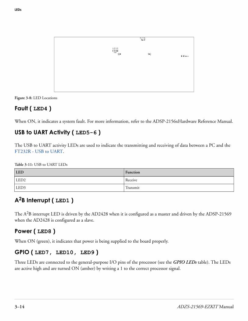
Figure 3-8: LED Locations
Fault ( LED4 )
When ON, it indicates a system fault. For more information, refer to the ADSP-2156xHardware Reference Manual.
USB to UART Activity ( LED5-6 )
The USB to UART activity LEDs are used to indicate the transmitting and receiving of data between a PC and theFT232R - USB to UART.
Table 3-11: USB to UART LEDs
LED Function
LED2 Receive
LED3 Transmit
A2B Interrupt ( LED1 )
The A2B interrupt LED is driven by the AD2428 when it is configured as a master and driven by the ADSP-21569when the AD2428 is configured as a slave.
Power ( LED8 )
When ON (green), it indicates that power is being supplied to the board properly.
GPIO ( LED7, LED10, LED9 )
Three LEDs are connected to the general-purpose I/O pins of the processor (see the GPIO LEDs table). The LEDsare active high and are turned ON (amber) by writing a 1 to the correct processor signal.
LEDs
3–14 ADZS-21569-EZKIT Manual

Table 3-12: GPIO LEDs
Reference Designator Programmable Flag Pin
LED7 PB_03LED9 DAI0_PIN08LED10 DAI0_PIN11
Reset ( LED11 )
When ON (red), it indicates that the board is in reset. A master reset is asserted by pressing SW2 , which activatesthe LED. For more information, see Reset Pushbutton ( SW2 ).
ConnectorsThis section describes connector functionality and provides information about mating connectors. The connectorlocations are shown in the Connector Locations figure.
Figure 3-9: Connector Locations
NOTE: Connectors on the back of the board are noted with dotted lines.
S/PDIF Optical Tx ( J1 )
Part Description Manufacturer Part Number
Fiber optic transmitter Everlight PLT133/T10W
Mating Cable
Standard TOSLINK optical digital cable
LEDs
ADZS-21569-EZKIT Manual 3–15

Clock ( J2 )
Part Description Manufacturer Part Number
SMB jack Emerson 131-3711-201
Mating Cable
Standard SMB cable
Audio Input/Output ( J3 )
Part Description Manufacturer Part Number
RCA 2x2 female Switchcraft PJRAS2X2S
Mating Cable
Standard audio cable with RCA connectors
Link Port/JTAG ( J8 and J9 )
Part Description Manufacturer Part Number
ERF8 10X2, female Samtec ERF8-010-05.0-D-DV-L
Mating Cable
6" coax cable assembly Samtec ERCD-010-06.00-TED-TEU-1-D
S/PDIF Optical Rx ( J11 )
Part Description Manufacturer Part Number
Fiber optic receiver Everlight PLR135/T10
Mating Cable
Standard TOSLINK optical digital cable
Audio Output ( J10 )
Part Description Manufacturer Part Number
RCA 4x2 female Switchcraft PJRAS4X2U
Mating Cable
Standard audio cable with RCA connectors
S/PDIF Digital ( J11 )
Connectors
3–16 ADZS-21569-EZKIT Manual

Part Description Manufacturer Part Number
RCA 1x2 female Switchcraft PJRAS1X2S02X
Mating Cable
Standard S/PDIF cable with RCA connectors
MLB ( J12 )
Part Description Manufacturer Part Number
40-pin high speed socket Samtec QSH-020-01-L-D-DP-A
Mating Connector
40-pin high speed header Samtec QTH-0202-01-L-D-DP-A
Headphone ( J13 )
Part Description Manufacturer Part Number
3.5mm headphone connector CUI SJ1-3525NG
Mating Cable
Standard audio cable with 3.5mm connector
HADC ( P1 and J4 )
Part Description Manufacturer Part Number
SMB jack Emerson 131-3711-201
Mating Cable
Standard SMB cable
JTAG ( P4 )
The JTAG header provides debug connectivity for the processor. This is a 0.05" shrouded through-hole connectorfrom SAMTEC (SHF-105-01-L-D-SM-K). This connector mates with ICE- 1000, ICE-2000, and any newer Ana-log Devices emulators. For more information, see Debug Interface
Sigma Studio ( P5 )
This connector interfaces with SigmaStudio® through the EVAL-ADUSB2EBZ board. The connector is a 0.1"header. The pinout can be found in the schematic.
Trace and JTAG ( P8 )
Connectors
ADZS-21569-EZKIT Manual 3–17

The Trace and JTAG connector provides connectivity to the processor's trace interface. This is a MICTOR connec-tor from TYCO (2-5767004-2). At this time, there are no trace pods available.
USB to UART( P11 )
Part Description Manufacturer Part Number
USB Micro-AB Hirose ZX62D-AB-5P8
Mating Cable
USB Micro-B to Standard-A cable
A2B ( P10 and P11 )
Part Description Manufacturer Part Number
2-pin DuraClik Molex 5023520200
Mating Cable
DuraClik cable assembly
Engine RPM ( P12 )
Part Description Manufacturer Part Number
IDC 2x1 0.1" Samtec HTSW-102-07-T-S
Mating Cable
Custom cable assembly
Microphone ( P13-P16 )
Part Description Manufacturer Part Number
IDC 2x1 0.1" Samtec HTSW-102-07-T-S
Mating Cable
Custom cable assembly
Power Plug ( P10 )
Part Description Manufacturer Part Number
2.1 mm power jack CUI PJ-102AH
Mating Cable
Connectors
3–18 ADZS-21569-EZKIT Manual

Part Description Manufacturer Part Number
[email protected] power supply CUI EMSA120150-P5RP-SZ
Power Terminal Block ( P22 )
Part Description Manufacturer Part Number
5.08mm power jack Weidmuller 1760510000
Mating Cable
12.0VDC discrete wires
Expansion Interface 3 ( P9 and P7 )
Part Description Manufacturer Part Number
120-pin, 0.6 mm Hirose FX8-120P-SV1(91)
Mating Connector
120-pin, 0.6 mm Hirose FX8-120S-SV(21)
Connectors
ADZS-21569-EZKIT Manual 3–19

ADZS-21569-EZKIT Manual 20

Mouser Electronics
Authorized Distributor
Click to View Pricing, Inventory, Delivery & Lifecycle Information: Analog Devices Inc.:
ADZS-21569-EZKIT