advd lecture 08 -inverte rpart3
TRANSCRIPT

Digital VLSI Design
• Full Automation
• Maximum benefit of scaling
• High speed ,
• low power
• Robustness
Power dissipation

Why worry about power?
-- Heat Dissipation
DEC 21164
microprocessor power dissipation

Why worry about power — Portability
Multimedia Terminals
Laptop Computers
Digital Cellular Telephony
BATTERY(40+ lbs)
Year
No
min
al C
ap
acity (
Wa
tt-h
ours
/ lb)
Nickel-Cadium
Ni-Metal Hydride
65 70 75 80 85 90 95
0
10
20
30
40
50
Rechargable Lithium
Expected Battery Lifetime increase
over next 5 years: 30-40%

Where Does Power Go in CMOS?
• STATIC POWER---NIL
• Dynamic Power Consumption
• Short Circuit Currents
• Leakage
Charging and Discharging Capacitors
Short Circuit Path between Supply Rails during Switching
Leaking diodes and transistors

Power consumption
• 4 components
Static power consumption
Short circuit power consumption
Leakage power consumption
Dynamic power consumption

• The total power in a CMOS circuit is given by Ptotal = Pd + Psc + Ps where
Pd is the dynamic average power (previous chart),
Psc is the short circuit power,
and Ps is the static power due to ratio circuit current, junction leakage, and sub-threshold Ioff leakage current
• Short circuit current flows during the brief transient when the pull down and pull up devices both conduct at the same time where one (or both) of the devices are in saturation

Static power consumption
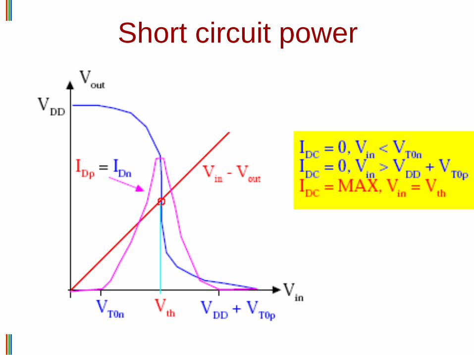
Short circuit power

CMOS Short-Circuit Power Dissipation
Derivation
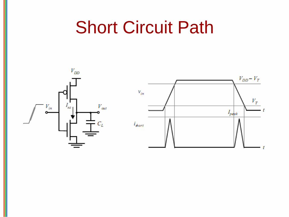
Short Circuit Path

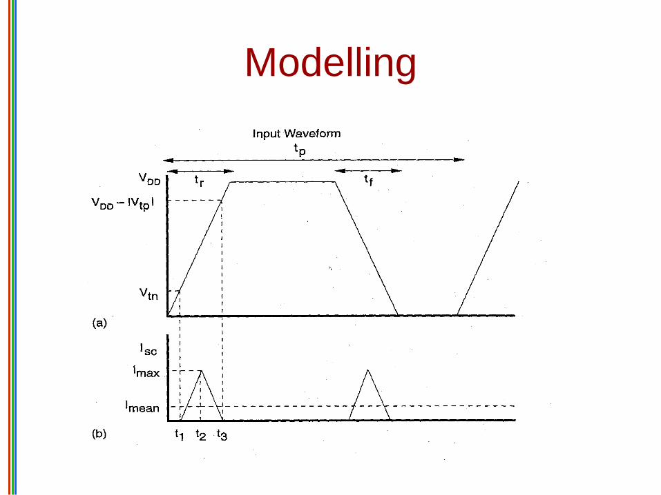
Modelling

t1- t2, Mos operates in saturation
At t2, current reaches its maximum value
At this point vin=vdd/2, because inverter is
symmetrical
I mean= 2x [2/T] x ∫Isat dt : Limits(t1, t2)
Conditions—Vin(t)=(Vdd/τ) t; --assume vin increases linearly with time
tr = tf = trf
Psc = (/12) (Vdd – 2Vt)3 (trf/tpin)

• For a balanced CMOS inverter with
n=p= , and Vtn = |Vtp|, the short
circuit power can be expressed by
Psc = (/12)(Vdd – 2Vt)3 (tr/f/tpin)
where tpin is the period of the input
waveform and trf is the input rise time
(or fall time) tr = tf = trf

Effect of load cap on short circuit
power
• P short circuit reduces
• Reason---- output start switching after
input has completely stabilized

Effect of Cload

Dynamic energy consumption

Energy stored across capacitor

Dynamic power consumption-derivation


Average Dynamic Power in CMOS
Inverter • Average dynamic power derivation:
– On negative going input, pull-up
device charges the load
capacitance. On positive going
input, pull-down device discharges
the load into ground.
– Average power given by
Pave = (1/T)CL (dvout/dt) (Vdd – vout)dt
+ (1/T)(-1) CL (dvout/dt) vout dt
where the first integral is taken from
0 to T/2 and the second integral is
from T/2 to T
• completion of the integral yields
Pave = CL Vdd2 f where f = 1/T
• Note that the dynamic power is
independent of the typical device
parameters, but is simply a
function of power supply, load
capacitance and frequency of
the switching!

Vin Vout
CL
Energy/transition = CL * Vdd2
Power = Energy/transition * f = CL * Vdd2 * f
Need to reduce CL, Vdd, and f to reduce power.
Vdd
Not a function of transistor sizes!

Reduce power consumption
• Reduce Vdd
• Reduce swing at the output
• Reduce CL
• Reduce Switching activity
To keep same speed, can we reduce Vdd, increase (w/L)? No
Inc in W inc in CL

Dynamic Power Consumption - Revisited
Power = Energy/transition * transition rate
= CL * Vdd2 * f01
= CL * Vdd2 * P01* f
= CEFF * Vdd2 * f
Power Dissipation is Data Dependent
Function of Switching Activity
CEFF = Effective Capacitance = CL * P01

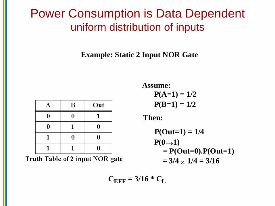
Power Consumption is Data Dependent uniform distribution of inputs
Example: Static 2 Input NOR Gate
Assume:
P(A=1) = 1/2
P(B=1) = 1/2
P(Out=1) = 1/4
P(01)
= 3/4 1/4 = 3/16
Then:
= P(Out=0).P(Out=1)
CEFF = 3/16 * CL


Transition Probabilities for Basic Gates
Non-uniform distribution of inputs

No feedback

Power consumption—Correlated signals
½ 1


Sizing for min. power
consumption
For a given delay constraint

Sizing for power consumption


Vdd=Vddref

Vdd=Vddref

Vdd≠ Vddref


Graphical solution

Why energy reduces for F increasing?
• Assume delay reqd is tpref=5ns.
• As F inc CL inc. delay (tp) inc. and dyn. energy inc.
linearly
• But as f inc delay reduces exponentially, energy inc.
• for F= 1 delay is already small and close to tpref). Inc in f
does not cause much reduction rather energy increment is
more
• For F large, delay and energy are large values
• Hence as f inc., delay reduces drastically (become less than
tpref ). Hence to have given delay= tpref, energy is dec.
which inc. delay to tpref.
• As f is increased further, delay reduction reduces, only
energy increases

Design example—0.25um technology, find f, Vdd for
tpref=0.2ns. Cext=10Cg1, γ=1, Vref=2.5v

Design a chain of inv for min delay, min energy
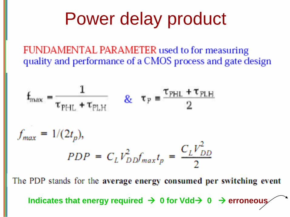
Power delay product
Indicates that energy required 0 for Vdd 0 erroneous

Energy delay product
Shd. Be minimum

Energy delay product optimum Vdd