advantages and challenges of silicon in the...
TRANSCRIPT

Final Term Paper
Advantages and challenges of silicon in the photovoltaic cells
by
Vishal Bharam
Due Day: 4th
May 2012

2
Abstract
Due to the high energy demands followed by the crisis of petroleum, the hope for the future lies
in the renewable energy resources such as solar energy. Photovoltaic cells with materials involving,
mainly silicon in both crystalline and amorphous form are used in this industry. This paper elaborates on
the characteristic of both crystalline and amorphous silicon that makes it worth to use them in the
photovoltaic cell. However, there are a lot of challenges involved in their use in the cell such as high
manufacturing cost, loss of material for crystal silicon while issues affecting the efficiency negatively in
terms of amorphous silicon. In response, solutions have been suggested in terms of both alternatives
manufacturing methods and materials used in the photovoltaic cells. The paper further explains the pros
and cons related to the suggestions involving changes in the production methods (Czochralski method)
and pushes the idea of using new material such as organic materials involving polymers (P3HT/PCBM)
along newly invented nanomaterial. The paper ends with introducing the concept of tandem cell
comprising two distinct devices stacked on top of each other, which allows absorbing light with wider
range of wavelength.

3
Table of content Page No.
1. Background 3
2. Types of Photovoltaic Cells 4
3. Photovoltaic Materials 6
4. Silicon in Photovoltaic Cells 6
4.1 Pure Crystalline Silicon 6
4.2 Amorphous Silicon 9
5. Challenges of Silicon in Photovoltaic Cells 10
5.1 Single Crystalline Silicon 10
5.2 Polycrystalline Silicon 11
5.3 Amorphous Silicon 12
6. Coping with the challenges
6.1 Alternative methods 12
6.2 Alternatives for Silicon 13
7. Conclusion 15
8. References 16

4
1. Background:
Today, the nonrenewable energy resources such as petroleum, coal, natural gas are depleting at
very high rate. Even though nuclear energy has been a consistent source of energy for a very long period,
doubts have been raised about its continuation after the last year’s Japan disaster. Due to this decrease in
the traditional energy sources, the demand for the alternatives energy resources has started to rise. To
meet this increasing demand with keeping environmental concerns in mind, people are thinking about
increasing use of renewable energy sources such as wind and solar energy. Since the sun is an energy
source, which will never get exhausted, it can be used without thinking about shortage of supply of
sunlight. The amount of sunlight that falls on the surface of the earth and can be effectively used ranges in
amounts of 89,000 terawatts per year. Thus, solar energy can be seen as an emerging source of energy.
During the last quarter of the century, solar generation of electricity has been proven technically
feasible and reliable. Despite these advantages, the observation of the following diagram suggests that
even after many years of invention of photovoltaic effect, its use to produce electricity has been very
limited. A study by International Energy Agency (IEA) shown that from 1973 to 2008, the use of all
renewable energy resources including solar, wind and heat have shown a dramatic increase [1]. However,
the use of all of these renewable resources still only accounts for less than 1% of overall energy use. Even
today, oil, coal and natural gas, which still counts for over 60% along with nuclear energy, have been the
most used energy resources.
Figure 1: Total worldwide energy supply of 1973 and 2008 [1]
There are different ways of utilizing the natural sunlight. Solar technologies are broadly
characterized into two different categories known as passive or active, depending on the way they
capture, convert and distribute solar energy. Active solar technologies involve the use of solar panels and
solar thermal collectors to use the solar radiation. Passive technologies basically include the building
structure to provide sunlight to all rooms, where thermal and insulating mechanisms are built into the

5
house to generate proper heating and cooling system, all without the use of any extra apparatus. What I
am mainly concerned about is active solar technologies involving photovoltaic effect.
So far, solar photovoltaic energy conversion has been used as the premium energy source in most
of the orbiting satellites. Silicon has been the most used material in most of the successful photovoltaic
cells. Two different forms of silicon, pure silicon and amorphous silicon are used to build the cells.
However, the use of the photovoltaic cells has been limited due to high processing cost of high purity
single crystal material used and the lack of effective mass production techniques used to produce thin
silicon films. Though single-crystalline silicon solar cells have been most efficient and advanced of all
cells, it is hard to implement them due to the cost factor. Thus, alternatives to silicon in the form of thin-
film materials such as cadmium telluride and Copper-Indium:Diselenide (CIS) are being considered
today. This overall paper further discusses in details, the advantages and challenges of using different
forms of silicon in photovoltaic cells.
2. Types of photovoltaic cells
Energy of the solar radiation is converted into electric energy through the photovoltaic effect.
Edmund Becquerel was first scientist to discover the photovoltaic effect and it was observed in a liquid
electrolyte. [2] Later work on Se, Cu-Cu2O, PbS, TlzS, AgzS, and many other materials known as
photoconductors or phosphors showed that the photovoltaic effect is very common in some specific
material. Later this photovoltaic effect was discovered in material such as silicon, GaAs and other
material and its usefulness for technical applications such as solar energy was later developed.
A discontinuity or marked changes in the materials used have been found very common in all
photovoltaic cells [3]. This discontinuity has been responsible for the creation of a potential, resulting in
the separation of photo-generated charge carriers. This build-in potential is used for the power generation
of the solar cell. According to the type of the change or discontinuity, there are two kinds of primary
photovoltaic cells, homo-junction and hetero-junction.
The discontinuity in homo-junction cell is in the type of the conductivity of the material from n-
type to p-type [4]. The region over this discontinuity change occurs is called as the p-n homo-junction.
Homo-junctions are generally found in the elemental semiconductors such as Si and Ge, or the compound
semiconductors such as GaAs and CdTe. Hetero-junctions are the combination of two different kinds of
semiconductor in either a graded or abrupt fashion. The discontinuity in the hetero-junction photovoltaic
cells occurs in the material characteristics such as carrier densities, electron affinity, conductivity, energy
band gap along with dielectric constants. The examples of the hetero junctions are n-CdS/p-Cu2S, n-
CdS/p-InP and many others. Along with these two kinds of discontinuities, one more type is also found in
the cell with metal-semiconductor combination. This discontinuity created by certain metal-
semiconductor combinations produces a sufficient enough potential to cause an asymmetric carrier flow
and is designated as a Schottky diode. In this cell, the metal is applied as a thin transparent layer, while
semiconductor is used to generate the excess carriers. The known Schottky diodes are n-GaAS/Au, n-
Si/Cr(Cu) and p-Cu2O/Cu.
The most common material in which the photovoltaic effect occurs are semiconductors, which lie
between metals and the insulators in terms of the conductivity. At low temperature, electrons in
semiconductors are in energy level known as full valence band, where they occupy a lower, stable energy
state. But increasing temperature allows more electrons to transit from the full valence band to the

6
conduction band. In this energy state, the electrons experience vibrations within the atomic lattice of the
material. The energy required for this transition of the levels is known as band gap energy.
3. Photovoltaic material:
To be practically useful and commercially reliable, the photovoltaic cells need to be affordable,
efficient and stable. It is really important that the price of the photovoltaic cell is within the affordable
range, so that it can compete with other source of energy. Furthermore, while building the acceptable
solar cell, it is really important to keep in mind the length of operating life, which is usually set at about
twenty years. While talking about the stability of the photovoltaic cells, is clear that a cell must remain in
operating condition for a period of time such that the energy produced by the cell is appreciably greater
than energy required for the production of the cell. In order for the photovoltaic cells achieve these goals,
they needs to be constructed with the material that can satisfy these goals. The semiconductor used needs
to have a low enough energy band gap to absorb the solar spectrum effectively and to control the
electrical processes involved in energy conversion. Given this, it is very clear that the material used in the
photovoltaic cells play a major role in its functioning.
Given a long range of material mentioned above, one might think that there is abundance of the
material to be used in the photovoltaic cell, but it still remain true today that only a relatively small
number of materials have met the basic criteria. Semiconductor and semiconductor compounds such as Si,
GaAs, InP, CdTe, and CuInSe2 are used in the single crystal cell, while hydrogenated amorphous silicon
(a-Si: H), CdTe, and CuInSe2 are generally use to produce the thin film with efficiency greater than 10%.
Recent research has also investigated the use of multi-junction cells in which two (or more) different cells
are used together, to produce the energy more efficiently [5]. One of the landmarks of 1988 was the
achievement of a 31% efficient solar cell with a combination of a single-crystal GaAs (with efficiency of
27.2% when used alone) along with a back-contact single-crystal Si (with efficiency of 26% when used
alone).
4. Silicon in photovoltaic cell:
Among all of the materials listed above, silicon is the most commonly used material in the
photovoltaic cells. It is also present in abundance in nature as silicon dioxide in sand and quartz, from
which it is extracted by reduction with carbon.[6]
In fact, silicon accounts for about 26% of the earth’s
crust. In the photovoltaic cells, two different forms of silicon are being used such as pure crystalline
silicon and the amorphous silicon. Due to the change in the structure, there are a lot of difference in terms
of physical properties of pure crystalline silicon and amorphous silicon.
4.1 Pure Crystalline Silicon
4.1.1 Single crystalline silicon
Pure crystalline silicon does not have the most desirable properties required for the photovoltaic
cells. Thus, in order to use pure crystalline silicon effectively in the photovoltaic cell, it needs to go
through a lot of processing. Though pure silicon is a bad conductor of the electricity, it can doped with
material like phosphorous and boron, as discussed above. There are also other physical properties that
characterize the silicon are discussed briefly below.

7
Energy band gap, which is the energy needed to shift electron from valence to conduction shell, is
one of the characteristics that define the electrical properties. Silicon has energy band gap of about 1.1eV,
which is sufficient enough to absorb most of the photon with the energy band gap higher than 1.1eV.
However, as temperature increases, the band gap decreases allowing silicon of capable to absorbing
photons with energy band gap less than 1.1 eV. The energy band gap height relationship with temperature
is given by: .[7]
Figure 4(a) represents energy bang gap as a function of
decreasing temperature.
(a) (b)
Figure 2: (a) Energy band gap [7]
and (b) intrinsic carrier concentration [8]
as function of decreasing temperature
Another important property that makes silicon worth to be used in the cell is the intrinsic carrier
concentration. Intrinsic carriers are the silicon electron in conduction band. The concentration of intrinsic
carrier is found as: , where k is Boltzmann’s constant [8]. The relationship
between the intrinsic carrier concentration and temperature is given in figure 4(b).
Silicon has very high carrier
mobility, the rate at which the carriers move
under the influence of electric field, that
differentiates it from other semiconductors.
For low electric field, the drift velocity in
terms of the electric field and the mobility is
as: , where μ is the mobility and
E is electric field [9]. The figure nearby
represent the carrier mobility in
phosphorous and boron doped silicon.
Figure 3: Carrier mobility in phosphorous and boron doped silicon [9]

8
One more characteristic that really influence the decision of using silicon over any other kinds of
materials mentioned above is its non-hazardous properties. As silicon is a non-toxic material, it has very
low effect on the environment. These all characteristic of silicon makes it worth to be used in the
photovoltaic cell. Since almost all of the industries related to electronics and communication operate with
silicon as their prime semiconductor material, there is already a large scope and wide array of
technological tools for processing and manufacturing silicon according to specific needs.
According to measure of efficiency, which is determined by fill factor (Ef = Voc/Isc), solar cells
are divided into monocrystalline and polycrystalline cell. There is a trade-off between efficiency of
photovoltaic cell and producing energy of cell. The brief details of these cells are discussed below.
4.1.2 Monocrystalline cell:
Single crystal or mono crystalline silicon is a continuous crystalline
material with no grain boundaries. The entire structure is one extensive
crystalline structure. There is a uniform molecular structure for all the silicon
atoms, with each of the four valence electrons of a silicon atom linked to
another silicon atom, as shown nearby. This is most efficient of all available
photovoltaic cells, with efficiency ranging within 25-30%. It is manufactured
using the Czochralski method, which needs a huge amount of energy.
Figure 4: The continuous structure of single-crystalline Silicon [10]
In this method, silicon is extracted from silicon dioxide and melted in a quartz crucible along with
the dopant material (phosphorous and boron) [11]. A single crystalline silicon seed is
then dipped into the molten liquid to initialize crystallization. The seed is then
pulled out slowly; the temperature and the rate of pull determines the rate of growth
of the resulting mass of mono crystalline silicon, known as the ingot. This mass of
crystal, which contains only mono crystalline silicon with dopants all throughout, is
then cut into slices and these slices are further processed into very thin wafers, range
in thickness from 200-300 micrometers [12]. The wafers are then coated with a
special layer of anti-reflective material of silicon nitride. These wafers are
connected together in either series or parallel, forming the solar panel, as shown.
Figure 5: Monocrystalline solar panel
4.1.3 Polycrystalline cell
Polycrystalline silicon is made of several small grains of mono crystalline silicon, with several
grain boundaries between the individual crystals. Polycrystalline cell, about 17% efficient, is most
commonly prepared by using molten liquid silicon mixed with dopants [13]. Instead
of crystallization, the molten liquid is cooled in a block-shaped cast. The rate of
cooling determines the size of the crystal grains and the distribution of the dopants
in the mixture. After cooling, the resulting ingot is sliced into thin portion, usually
square in shape by passing the ingot through metal wires. These cells are
connected together forming a polycrystalline solar panel. Thus, the manufacturing
of polycrystalline silicon cells is much simpler and cheaper than that of mono
crystalline silicon.
Figure 6: Polycrystalline solar panel
9
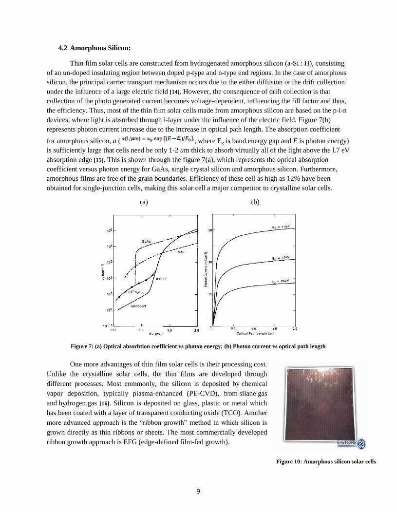
4.2 Amorphous Silicon:
Thin film solar cells are constructed from hydrogenated amorphous silicon (a-Si : H), consisting
of an un-doped insulating region between doped p-type and n-type end regions. In the case of amorphous
silicon, the principal carrier transport mechanism occurs due to the either diffusion or the drift collection
under the influence of a large electric field [14]. However, the consequence of drift collection is that
collection of the photo generated current becomes voltage-dependent, influencing the fill factor and thus,
the efficiency. Thus, most of the thin film solar cells made from amorphous silicon are based on the p-i-n
devices, where light is absorbed through i-layer under the influence of the electric field. Figure 7(b)
represents photon current increase due to the increase in optical path length. The absorption coefficient
for amorphous silicon, a ( , where Eg is band energy gap and E is photon energy)
is sufficiently large that cells need be only 1-2 um thick to absorb virtually all of the light above the l.7 eV
absorption edge [15]. This is shown through the figure 7(a), which represents the optical absorption
coefficient versus photon energy for GaAs, single crystal silicon and amorphous silicon. Furthermore,
amorphous films are free of the grain boundaries. Efficiency of these cell as high as 12% have been
obtained for single-junction cells, making this solar cell a major competitor to crystalline solar cells.
(a) (b)
Figure 7: (a) Optical absorbtion coefficient vs photon energy; (b) Photon current vs optical path length
One more advantages of thin film solar cells is their processing cost.
Unlike the crystalline solar cells, the thin films are developed through
different processes. Most commonly, the silicon is deposited by chemical
vapor deposition, typically plasma-enhanced (PE-CVD), from silane gas
and hydrogen gas [16]. Silicon is deposited on glass, plastic or metal which
has been coated with a layer of transparent conducting oxide (TCO). Another
more advanced approach is the “ribbon growth” method in which silicon is
grown directly as thin ribbons or sheets. The most commercially developed
ribbon growth approach is EFG (edge-defined film-fed growth).
Figure 10: Amorphous silicon solar cells

10
5. Challenges of silicon in photovoltaic cells
Due to the efficiency, most of the solar cells are constructed using the single crystalline silicon.
The effectiveness of monocrystalline solar cells mostly lies in the fact that it does not have the grain
boundaries due to its continuous structure, which means the excited electrons move around the silicon
structure without any grain boundaries to obstruct their movement. On the other hand, there lie several
grain boundaries in the polycrystalline cells which inhibit the continuous flow of the excited electrons in
the semiconductor, leading to a radical drop in efficiency to about 10-15% [17]. Therefore, research has
been developed for finding the solar cell balancing the cost-effectiveness and performance. Even though a
thin film solar cell made by amorphous silicon seems to a be a good replacement, they are suffering in
terms of efficiency, mainly due to the lack of a uniform crystalline structure. Some of these issues are
discussed in details below:
5.1 Single Crystalline Silicon:
5.1.1 Cost of processing:
The Czochralski method, which is used to manufacture the monocrystalline silicon cells, needs a
lot of energy. Since single crystal silicon needs to pure in order for its crystalline structure to be highly
uniform, a lot of processing needs to bring it to that level. Silicon used for single crystal silicon may need
to have an impurity concentration of as low as 10-10
% [18]. Extremely precise control and balance of the
single crystal silicon seed is required in order to generate an ingot that has mono crystalline silicon all
throughout. Also, during the procedure, oxidation of the ingot is also an unavoidable consequence as
oxygen combines with the silicon as well as the dopants on the surface of the ingot. This combined
oxygen later on hampers the flow of charge carriers/electrons in the cell, decreasing the efficiency. This
overall complicates the procedure, and hence, increases cost.
5.1.2 Loss of material:
In order for the single crystal silicon to be modulus, it needs to in sliced in wafers of thickness
ranging from 200-300 μm. For this purpose, an inner diameter saw is used. This saw employs diamond
particles on its blade for sawing the ingots into fine wafers [19]. It is difficult to employ any kind of saw
mechanism, because at the desired thickness level of the wafers (200-300 μm), they tend to break easily.
However, while the wafers are manufactured using this mechanism, about 50% of the produced silicon
gets lost as sawdust, mainly due to the sawing in this process.
5.1.3 Problems with absorption:
A general structure of the solar panel includes a glass on top for
protection from wind, the photovoltaic cell with antireflective coating in
the middle with a metal to support at the bottom. Each layer in the cells is
characterized by a complex refractive index (N = n-ik), where n is real
refractive index of material and k is the extinction coefficient.
The absorption factor of the solar cells (α) is equals: α = 4πk/λ.
However, according to this equation, as the wavelength of photons
increases, the absorption coefficient decreases [20]. Photons with short
Figure 11: Absorption as a factor of wavelength [20]
11
wavelength (λ<1.0) have an energy larger than the band gap, which allows it to generate electron–hole
pairs and is readily absorbed by the crystalline silicon. This wavelength of light/photons usually includes
the infrared spectrum. However, long-wavelength photons (λ>1.2 μm) cannot generate electron-hole pairs
and are hardly absorbed. Photons in the transition region of (1.2 μm <λ<1.0 μm) are weakly absorbed.
This means, light with higher wavelength (λ>1.2 μm), is not utilized by the solar cell.
5.2 Polycrystalline silicon:
We know that, when the photon with different wavelength strike the surface of photovoltaic cell,
it create an electron-hole pair. In the case of a hole formed at the p-n junction, electrons coming from the
top surface are captured by the holes on the top surface and in the same way, the holes created in the
bottom layers will capture the electrons coming from the junction. This overall decreases electron flow
resulting in overall decrease in the current generated in the cell. This is a common problem with
crystalline silicon cells because they are made thicker than other. Thus, a lot of recombinational loss
occurs which decreases the overall efficiency.
The polycrystalline cell contains a certain degree of thickness, higher than that of monocrystalline
cell. As these cells are made of several single-crystal molecules, it has a lot of grain boundaries, which are
primarily composed of regular line defects: simple dislocations, partial dislocations, and stacking faults
[21]. Two methods are used to measure the grain boundaries in the polycrystalline silicon, known as I-V
deconvolution and charge emission. The first one involves the measurement of trans-barrier current, while
the latter one is a high frequency barrier capacitance determination [22]. Among the two methods given
below, the I-V deconvolution method is most used one. Here, the trans-barrier current is measured as:
, where A* is the effective Richardson constant. The supply function,
n(E), is calculated by appropriate k space integration, and the transmission probability, D(E), is estimated
using the WKB approximation [23]. This expression explains the inverse relationship between the grain-
boundaries and the current flowing through the cell. When the grain boundary is associated with a dc bias,
the above equation can be expressed as:
, which
shows that the quasi Fermi level at the grain boundary is
pinned (for V > kT/e) for the value close to the more
negative grain [24]. Once the position of the quasi-Fermi
level at the grain boundary plane is established, ϕB as a
function of bias is determined. Using this expression, the
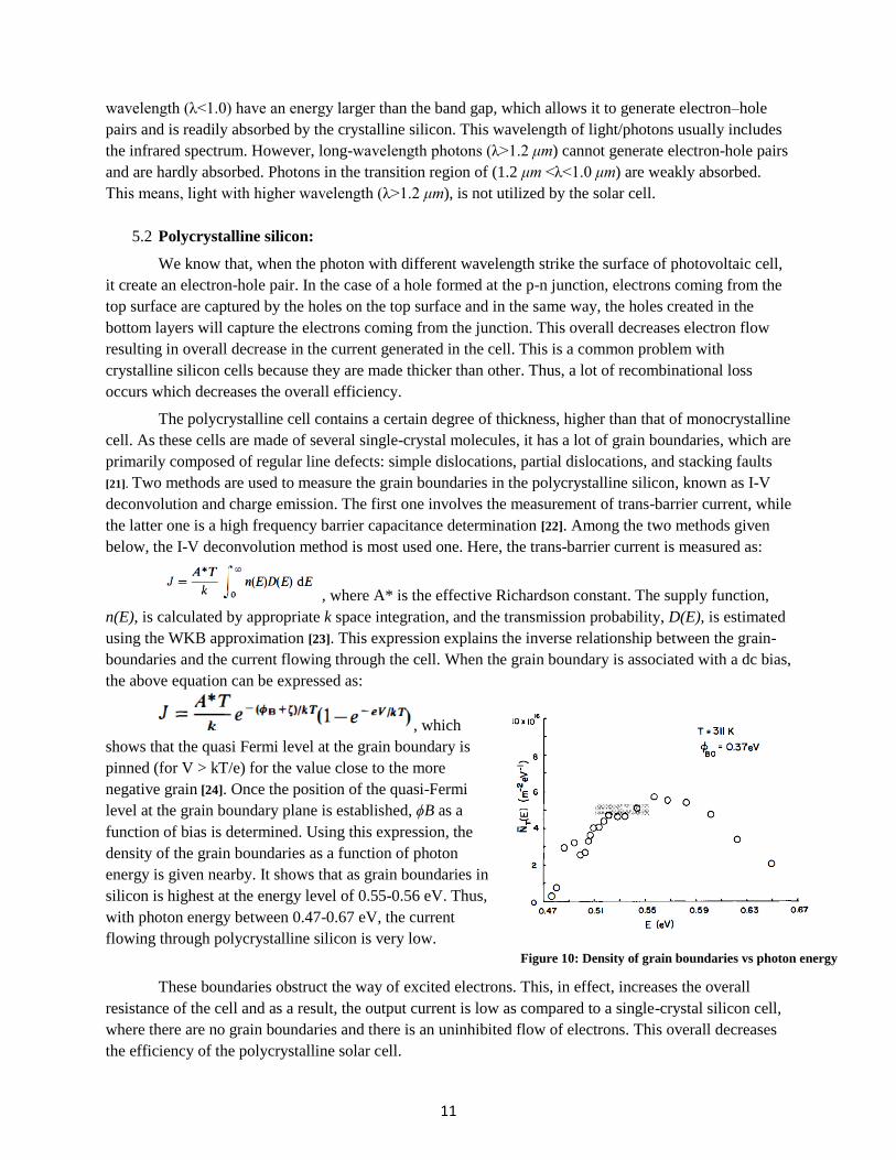
density of the grain boundaries as a function of photon
energy is given nearby. It shows that as grain boundaries in
silicon is highest at the energy level of 0.55-0.56 eV. Thus,
with photon energy between 0.47-0.67 eV, the current
flowing through polycrystalline silicon is very low.
Figure 10: Density of grain boundaries vs photon energy
These boundaries obstruct the way of excited electrons. This, in effect, increases the overall
resistance of the cell and as a result, the output current is low as compared to a single-crystal silicon cell,
where there are no grain boundaries and there is an uninhibited flow of electrons. This overall decreases
the efficiency of the polycrystalline solar cell.

12
5.3 Amorphous silicon:
Thin film solar cells are seen as competitor to the crystalline silicon due to their cost and
efficiency tradeoff. However, there are several major aspects of amorphous silicon that requires further
development: (a) a poor minority-carrier lifetime, (b) degradation of cell performance due to illumination,
(c) difficulty in materials dopant and (d) poor-quality alloys.
“The disordered nature of amorphous silicon leads to a high density of states within the forbidden
energy gap, in the form of band tail states and dangling bonds” [25]. Due to this, both the mobility and
lifetime of free carriers are substantially reduced compared to those of crystalline materials. Furthermore,
the absolute quantum efficiency, which is the percentage
of photons hitting the photo reactive surface that will
produce an electron–hole pair, decreases as the
wavelength of light increases. The figure nearby
represents the absolute quantum efficiency (QE) as a
function of light wavelength. The shapes of the curves
indicate that the quantum efficiency for wavelengths
longer than 0.6 μm is determined by the soft absorption
edge of the i-layer. For shorter wavelengths, the QE is
decreasing as it is determined by the photon absorption in
the p-layer, from which no carriers are collected. There is
also no charge carrier flow for the wavelength higher
than 0.8 μm.
Figure 12: Absolute QE as a function of wavelength
6. Coping with the challenges:
Although, crystalline solar cells are used widely in the market today, issues associated with
silicon are preventing the demand of the solar energy to increase. Though single crystalline silicon is very
efficient relative to other kinds of the solar cells, the cost factor overrules its advantage with the
efficiency. For polycrystalline silicon, the reduction in cost during the manufacturing stages by simple
cooling of molten silicon makes it less efficient. Though, thin film is seen as competitor to the
monocrystalline cell, development is still required for the issues related to poor minority carrier and lower
quantum efficiency in amorphous silicon. Thus, in order to use the photovoltaic effect to its highest
potential, it is important to find either the solution to the problems associated with silicon or other
materials which can implement the photovoltaic effect in exclusive and cheaper ways.
6.1 Alternative methods:
There is still a lot of research is being done in terms improving the quality of silicon by
overcoming the challenges. However, it is hard to find accessible solutions for the problems related to the
characteristics of the material itself, such as absorption problem, grain boundaries. Because, it involves
very complex methods in order to alter natural properties of the materials. Therefore, most of the research
is based on changing the process of building the solar cells. Below are some suggestions provided:
In order to decrease the cost of sing crystalline cell production, there are many suggestions
provided to modify the Czochralski method. The general approach is to reduce the amount of Si material
used in wafer-Si cells. This can be realized by reducing the thickness of the Si wafer and reducing the
material loss during ingot slicing. Furthermore, more approaches include directional solidification for

13
growth of poly-Si ingots, which requires ~12 kWh/kg of electricity versus ~100 kWh/kg for the
Czochralski process [26]. Another example is screen printing for metallization, which prints Al and Ag
pastes into various shapes for electrical contacts. In this method, thick film technology is used, which
lends itself much more to automation than the conventional vacuum evaporation [27].It is easy to fully
automate, so it gives a cost reduction of the processing of 60% to 80%. Though there are a lot of other
suggestions, one of the issues with them is that they are not efficient compared to the Czochralski method.
Therefore, scientists are still searching options with cost reduction as well as efficiency.
In order to combat the recombinational losses, it is suggested to infuse a thick concentration of
holes or atoms with vacant orbitals in the bottom layer of the cell [28]. This will ensure that the holes
formed by the photons diffuse towards the upper layers and do not recombine with the electrons produced
by the excitation of photons. However, it is quietly costly to implement this method for larger production.
One of the issues related to the general solar cell is the reflection loss, which can be calculated as:
, where R(λ) is reflectivity of silicon, ϕ(λ) is the photon incident on the surface and
a(λ) is the absorption coefficient of silicon. Along with these factors,
reflection also depends on the glass and anti-reflective coating used in
the panel as shown in the figure nearby [29]. This shows that reflection
loss can be controlled with use of appropriate glass and antireflective
material. For decreasing the reflectance of the surface of the
crystalline silicon cells, newer antireflective materials are being
considered. One of them is silicon nitride, which promises a lower
reflectance. Also, for decreasing reflectance, another recent
development is etching of the surface of the silicon cell in order to
give it an irregular dented surface [30]. This is done by using a solution
of sodium hydroxide or potassium hydroxide (10-30% concentration)
to acidify and corrode the surface.
Figure 13: Reflection of solar panel under different conditions
6.2 Alternatives for silicon
Along with the change in manufacturing method, alternatives for silicon are also being
considered. Material like Gallium Arsenic (GaAs), Cadmium Telluride (CdTe), Copper-
Indium:Diselenide (CIS) and Copper-Indium:Gallium-Diselenide (CIGS) is also being considered as the
replacement for silicon in the solar cells. Among all of them, CIS and CIGS are also useful due to the
remarkably high efficiency for polycrystalline thin films, at 18.8% in the laboratory, because of a band
gap of 1.1-1.2 eV [31]. However, they are unstable and unreliable in conservable heat and humanity.
Furthermore, there are problems with the availability and price of Indium. CdTe is also considered due its
high optical absorption and variety of deposition techniques (e.g. close-spaced vapor transport, electro-
deposition, and screen printing) producing a variety of junction structures [32]. However, problem
associated with CdTe is its difficulty in controlling the doping and achieving stable, low resistance
contacts to p-type CdTe. The biggest problem of this cell is its disposal due to use of hazardous Cd.
Along with these materials, research has been developing for the use of organic and nono-
crystalline particles in the photovoltaic cells. Organic photovoltaic cell (OPV) have became highly
popular in last decade [33]. OPV cells contain at least one organic semiconductor or molecule under the
effect of active light absorbing layer. The different kinds of sells produced under this technique include
14
solid-state dye-sensitized cell and hybrid solar cells, which is produced by either dispersing inorganic
nanoparticles into a semiconducting polymer matrix or combining inorganic nanostructured
semiconductor such as ZnO or TiO2 with organic semiconductors. The development of the OPV cells
started with the invention of bulk hetero-junction (BHJ), where donor are acceptor materials were mixed
together to form the higher efficiency cells.
Among all of OPV cells, a lot of research has been being done throughout last decade on
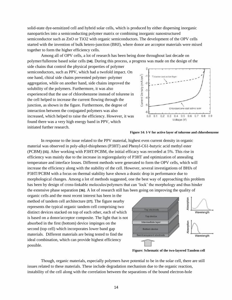
polymer/fullerene based solar cells [34]. During this process, a progress was made on the design of the
side chains that control the physical properties of polymer
semiconductors, such as PPV, which had a twofold impact. On
one hand, chiral side chains prevented polymer–polymer
aggregation, while on another hand, side chains improved the
solubility of the polymers. Furthermore, it was also
experienced that the use of chlorobenzene instead of tolurene in
the cell helped to increase the current flowing through the
junction, as shown in the figure. Furthermore, the degree of
interaction between the conjugated polymers was also
increased, which helped to raise the efficiency. However, it was
found there was a very high energy band in PPV, which
initiated further research.
Figure 14: I-V for active layer of tolurene and chlorobenzene
In response to the issue related to the PPV material, highest even current density in organic
material was observed in poly-alkyl-thiophenes (P3HT) and Phenyl-C61-butyric acid methyl ester
(PCBM) [35]. After working with P3HT/PCBM, the initial efficacy was recorded at 5%. This rise in
efficiency was mainly due to the increase in regioregularity of P3HT and optimization of annealing
temperature and interface losses. Different methods were generated to form the OPV cells, which will
increase the efficiency along with the stability of the cell. However, several investigations of BHJs of
P3HT/PCBM with a focus on thermal stability have shown a drastic drop in performance due to
morphological changes. Among a lot of methods suggested, one the best way of approaching this problem
has been by design of cross-linkable molecules/polymers that can ‘lock’ the morphology and thus hinder
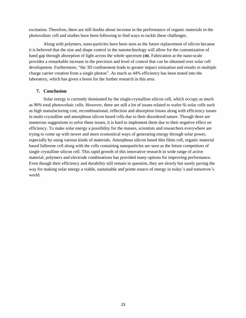
the extensive phase separation [36]. A lot of research still has been going on improving the quality of
organic cells and the most recent interest has been in the
method of tandem cell architecture [37]. The figure nearby
represents the typical organic tandem cell comprising two
distinct devices stacked on top of each other, each of which
is based on a donor/acceptor composite. The light that is not
absorbed in the first (bottom) device impinges on the
second (top cell) which incorporates lower band gap
materials. Different materials are being tested to find the
ideal combination, which can provide highest efficiency
possible.
Figure: Schematic of the two-layered Tandem cell
Though, organic materials, especially polymers have potential to be in the solar cell, there are still
issues related to these materials. These include degradation mechanism due to the organic reaction,
instability of the cell along with the correlation between the separations of the bound electron-hole
15
excitation. Therefore, there are still doubts about increase in the performance of organic materials in the
photovoltaic cell and studies have been following to find ways to tackle these challenges.
Along with polymers, nano-particles have been seen as the future replacement of silicon because
it is believed that the size and shape control in the nanotechnology will allow for the customization of
band gap through absorption of light across the whole spectrum [38]. Fabrication at the nano-scale
provides a remarkable increase in the precision and level of control that can be obtained over solar cell
development. Furthermore, “the 3D confinement leads to greater impact ionization and results in multiple
charge carrier creation from a single photon”. As much as 44% efficiency has been tested into the
laboratory, which has given a boost for the further research in this area.
7. Conclusion
Solar energy is currently dominated by the single-crystalline silicon cell, which occupy as much
as 90% total photovoltaic cells. However, there are still a lot of issues related to wafer-Si solar cells such
as high manufacturing cost, recombinational, reflection and absorption losses along with efficiency issues
in multi-crystalline and amorphous silicon based cells due to their disordered nature. Though there are
numerous suggestions to solve these issues, it is hard to implement them due to their negative effect on
efficiency. To make solar energy a possibility for the masses, scientists and researchers everywhere are
trying to come up with newer and more economical ways of generating energy through solar power,
especially by using various kinds of materials. Amorphous silicon based thin films cell, organic material
based fullerene cell along with the cells containing nanoparticles are seen as the future competitors of
single crystalline silicon cell. This rapid growth of this innovative research in wide range of active
material, polymers and electrode combinations has provided many options for improving performance.
Even though their efficiency and durability still remain in question, they are slowly but surely paving the
way for making solar energy a viable, sustainable and prime source of energy in today’s and tomorrow’s
world.
16
8. References
[1]
International Energy Agency. 2010. Key World Energy Statistics. P: 8 [2]
Boer K, Rothwarf A. 1876. Material for Solar Photovoltaic Energy Conversion. www.annualreviews.org. p: 1 [3]
Boer K, Rothwarf A. 1876. Material for Solar Photovoltaic Energy Conversion. www.annualreviews.org. p: 2 [4]
Boer K, Rothwarf A. 1876. Material for Solar Photovoltaic Energy Conversion. www.annualreviews.org. p: 2
[5] Bube R. 1990. Materials for photovoltaic. www.annualreviews.org. p: 5
[6] Green M. 2001. Crystalline Silicon solar cells. Photovoltaic special research center. P:4
[7] Jones S. 2008. Properties of Silicon. IC Knowledge LLC. P: 9
[8] Jones S. 2008. Properties of Silicon. IC Knowledge LLC. P: 10
[9] Jones S. 2008. Properties of Silicon. IC Knowledge LLC. P: 13-14
[10] http://www.pveducation.org/pvcdrom/manufacturing/single-crystalline-silicon, 4/21/2012
[11] Green M. 2001. Crystalline Silicon solar cells. Photovoltaic special research center. P: 15-22
[12] Mah Oilvia. 1998. Fundamental of photovoltaic materials. National Solar Power Research Institute, Inc. p: 4
[13] Green M. 2001. Crystalline Silicon solar cells. Photovoltaic special research center. P: 22-27
[14] Mitchell A, Touryan K. 1985. Amorphous Silicon Alloys for Solar Cells. www.annualreviews.org. P: 8
[15] Mitchell A, Touryan K. 1985. Amorphous Silicon Alloys for Solar Cells. www.annualreviews.org. P: 6
[16] Mah Oilvia.1998. Fundamental of photovoltaic materials. National Solar Power Research Institute, Inc. P:4-5
[17] Mah Oilvia.1998. Fundamental of photovoltaic materials. National Solar Power Research Institute, Inc. P:4-5
[18] Goetzberger A, Knobloch J, Voss B, ed. 1998. Crystalline Silicon Solar Cells. England: Willey press
[19] Goetzberger A, Knobloch J, Voss B, ed. 1998. Crystalline Silicon Solar Cells. England: Willey press
[20] Santbergen R, Zolingen R. 2007. The absorption factor of crystalline silicon PV cells: A numerical and
experimental study. Science Direct. P: 1-2
[21] Seager C. 1985. Grain Boundaries in Polycrystalline Silicon. www.annualreviews.org. P: 4
[22] Seager C. 1985. Grain Boundaries in Polycrystalline Silicon. www.annualreviews.org. P: 22
[23] Seager C. 1985. Grain Boundaries in Polycrystalline Silicon. www.annualreviews.org. P: 13
[24]Seager C. 1985. Grain Boundaries in Polycrystalline Silicon. www.annualreviews.org. P: 23
[25] Mitchell A, Touryan K. 1985. Amorphous Silicon Alloys for Solar Cells. www.annualreviews.org. P: 6
[26] Tao M. 2008. Inorganic Photovoltaic Solar Cells: Silicon and Beyond. The Electrochemical Society Interfce P 34
[27] Frisson L, Mertens R, Oversteaeten R, Govertens R. 2008. Screen Printed Metallization of Silicon Solar Cells.
Eletrocomponent Science and Technology. 7:107-108 [28]
Photovoltaic Education Network. 2010. Antireflection Coating and Recombination Losses.
http://pveducation.org/ [29]
Photovoltaic Education Network. 2010. Antireflection Coating and Recombination Losses.
http://pveducation.org/ [30]
Goetzberger A, Knobloch J, Voss B, ed. 1998. Crystalline Silicon Solar Cells. England: Willey press [31]
Bertolli M. 2008. Solar Cell Materials. P: 7-9
[32] Bertolli M. 2008. Solar Cell Materials. P: 10-11
[33] Barbec C, Gowrisankar S, Halls J, Laird D, Jia S, Williams S. Polymer-Fullerene Bulk-Heterojunction Solar
Cells. Material Views. P: 3839-3840 [34]
Barbec C, Gowrisankar S, Halls J, Laird D, Jia S, Williams S. Polymer-Fullerene Bulk-Heterojunction Solar
Cells. Material Views. P: 3841-3843 [35]
Barbec C, Gowrisankar S, Halls J, Laird D, Jia S, Williams S. Polymer-Fullerene Bulk-Heterojunction Solar
Cells. Material Views. P: 3841-3843 [36]
Helgesen M, Sondergaard R, Krebs Frederik. 2009. Advanced materials and processes for polymers solar cell
devices. Journal of Material Chemistry. P: 8 [37]
Barbec C, Gowrisankar S, Halls J, Laird D, Jia S, Williams S. Polymer-Fullerene Bulk-Heterojunction Solar
Cells. Material Views. P: 3847-3848
[38] Bertolli M. 2008. Solar Cell Materials. P: 11-12