advances in helium ion microscopy for high resolution...
TRANSCRIPT

Advances in Helium Ion Microscopy For High Resolution Imaging, Analysis and Materials Modification
William B. Thompson, John Notte, Larry Scipioni,
Mohan Ananth, Lewis Stern, Sybren Sijbrandij and Colin Sanford
Carl Zeiss SMT, One Corporation Way, Peabody, MA 01960
ABSTRACT The rapidly increasing use of materials like carbon,
ceramics and soft organic materials in nanotechnology causes a number of challenges for materials imaging, characterization, analysis and modification. With its ‘Top Down’ 0.35 nm resolution and its ability to obtain surface sensitive images of uncoated insulating specimens, the helium ion microscope (HIM) is showing improved usefulness in addressing some of these imaging, characterization and analysis challenges. With the addition of controlled dose patterning, the HIM is further capable of modifying materials such as graphene, silicon, and magnesium oxide with dimensions at or below 10 nm. These modifications can be accomplished by either the physical processes associated with a pure ion/material interaction or by the chemical processes of ion induced etching and deposition. In what follows, we provide an overview of the machine architecture, a summary of the more important HIM material interactions and cover the system’s current level of imaging, analysis and material modification performance. Keywords: Helium Ion Microscope, Sub-nanometer imaging, Rutherford Backscatter Spectroscopy, Nanometer patterning, Graphene
1 INTRODUCTION
Currently, the Orion helium ion microscope (HIM) can
be operated in two main imaging modes; ion induced secondary electron (SE) mode and Rutherford backscatter imaging (RBI) mode. This paper will provide an overview of the microscope’s ion source, its ion optics, the system architecture, the fundamentals of the SE and RBI imaging modes and some material analysis and modification related examples.
A helium ion microscope SE mode image differs from an SEM image in that it provides high resolution, surface sensitive information, on both conductive and insulating samples without the need for any conductive coating, unlike a conventional SEM. HIM RBI mode, on the other hand,
contains considerable material and channeling contrast image content.
Recently integrated with the microscope is a Rutherford Backscatter (RBS) detector for materials analysis. The detector is a modified silicon diode drift detector with a collected pulse height that is proportional to the energy of the backscattered helium ion.
The high resolution beam induced modification of materials is an important nanofabrication technique with applications in material science, semiconductor processing, circuit edit, basic physics research and NEMS, for example.
The removal of material can be accomplished in the helium ion microscope through either sputtering; ion impact material loss induced by radiolysis and thermal effects or by ion beam induced etching.
The addition of material can only be accomplished by ion beam induced chemistry. To accommodate our customers, we have added a Gas Injection System (GIS) to the HIM to provide the user with the opportunity to perform ion induced chemistry research. Although both the etched and deposited dimensions of geometries generated with the helium ion beam are greater than the 0.35 nm beam diameter, these geometries are typically in the sub 10 nm regime and generally much smaller than those obtained by other lithographic patterning methods.
In addition to describing the machine architecture in the succeeding sections, we will cover these three main HIM application topics of imaging, RBS and HIM initiated material modification.
2 THE HIM ION SOURCE, OPTICS,
SYSTEM BASICS AND SECONDARY ELECTRON IMAGING
2.1 The HIM Ion Source
The system’s high resolution is the result of the virtual source for the helium ion probe being subatomic. The ion source consists of a single crystal metal needle sharpened to a three atom pyramid that sits at the apex of the needle. The needle is immersed in a helium atmosphere held at a temperature of approximately 77 degrees K at a voltage that is variable from 10 to 35 keV. Ions launched from one of
NSTI-Nanotech 2010, www.nsti.org, ISBN 978-1-4398-3401-5 Vol. 1, 2010 25

the three atoms are sent down the column to become the scanned HIM probe.
2.2 The HIM Optics
The microscope electrostatic optics contains a gun lens, deflectors and a final or objective lens. The ratio of source size to probe size is approximately 1:1, i.e. the column magnification is around 1. Hence in the absence of aberrations, the scanned probe would be of order atomic dimensions. The actual probe size, at 35 keV, is limited by chromatic aberrations to 0.2 nm. As a consequence of this probe diameter, SE mode resolution of the microscope is around 0.35 nm as is evident in the gold on carbon image of figure 1.
Figure 1: A 300 nanometer field of view, HIM SE, image of a gold on carbon sample with 0.35 nm resolution.
The high source brightness and low column
demagnification gives the microscope an unusually large, 2.5 m, depth of field. For the beam diameters available with this optics, beam currents in the 0.5 to 10 pA range are easily attainable. 2.3 The Helium Ion Microscope System
The design goal for the SE imaging mode of the microscope was TEM resolution without the need of elaborate sample preparation. For this reason, the work chamber module is supported by a double tiered vibration isolation system mounted on a granite table. Sample loading, stage motion and the user interface are very similar to that of conventional SEM. Figure 2 shows the overall helium ion microscope system.
For a more extensive description of the HIM source, optics and system one is referred to a previous microscope publication [1].
Figure 2: The Orion Plus Helium Ion Microscope
2.4 Secondary Electron Imaging
In many respects the microscope behaves and is operated in the same manner as an SEM. The primary difference being that the scanned probe is helium ions rather than electrons. When the high energy helium ions are scanned over a sample surface, they generate secondary electrons, backscattered ions and photons. The present microscope configuration uses an Everhart-Thornley (ET) secondary electron detector to form an SE image. A microchannel plate (MCP) is used to acquire a backscattered ion, or RBI image. This RBI image is generated by the video signal output of the MCP produced when the Rutherford backscattered helium from the sample impinges on the MCP detector. Both the SE and the RBI images can be acquired simultaneously and provide significantly different image information.
The energy transferred by the helium to the electrons of a sample is less than 10 eV and the energy of the electrons that escape from the sample is around 2 eV. As a consequence of these low energies and the short mean free path of the electrons in most materials, the only electrons that can escape from the sample have originated near the sample surface. HIM SE imaging is therefore a very surface sensitive imaging technique. The low SE electron energy also means that small changes in surface potential and work function will readily modify the image contrast. One implication of this effect is that low doping concentration changes in silicon are often detectable.
Any insulating or dielectric material imaged with a positive ion beam will invariably charge positively. This is not the case in an SEM in which samples can charge both negatively and positively. The ion induced positive surface charge can be neutralized in the HIM with low energy flood electrons. The helium ion microscope has been equipped with a low energy electron flood gun that permits those samples that might conceivably charge up to be imaged,
NSTI-Nanotech 2010, www.nsti.org, ISBN 978-1-4398-3401-5 Vol. 1, 201026
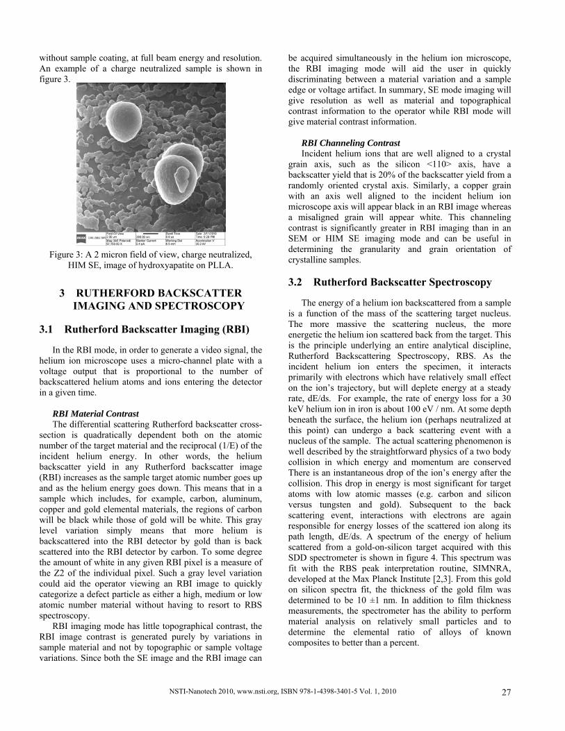
without sample coating, at full beam energy and resolution. An example of a charge neutralized sample is shown in figure 3.
Figure 3: A 2 micron field of view, charge neutralized, HIM SE, image of hydroxyapatite on PLLA.
3 RUTHERFORD BACKSCATTER
IMAGING AND SPECTROSCOPY
3.1 Rutherford Backscatter Imaging (RBI)
In the RBI mode, in order to generate a video signal, the helium ion microscope uses a micro-channel plate with a voltage output that is proportional to the number of backscattered helium atoms and ions entering the detector in a given time.
RBI Material Contrast The differential scattering Rutherford backscatter cross-
section is quadratically dependent both on the atomic number of the target material and the reciprocal (1/E) of the incident helium energy. In other words, the helium backscatter yield in any Rutherford backscatter image (RBI) increases as the sample target atomic number goes up and as the helium energy goes down. This means that in a sample which includes, for example, carbon, aluminum, copper and gold elemental materials, the regions of carbon will be black while those of gold will be white. This gray level variation simply means that more helium is backscattered into the RBI detector by gold than is back scattered into the RBI detector by carbon. To some degree the amount of white in any given RBI pixel is a measure of the Z2 of the individual pixel. Such a gray level variation could aid the operator viewing an RBI image to quickly categorize a defect particle as either a high, medium or low atomic number material without having to resort to RBS spectroscopy.
RBI imaging mode has little topographical contrast, the RBI image contrast is generated purely by variations in sample material and not by topographic or sample voltage variations. Since both the SE image and the RBI image can
be acquired simultaneously in the helium ion microscope, the RBI imaging mode will aid the user in quickly discriminating between a material variation and a sample edge or voltage artifact. In summary, SE mode imaging will give resolution as well as material and topographical contrast information to the operator while RBI mode will give material contrast information.
RBI Channeling Contrast Incident helium ions that are well aligned to a crystal
grain axis, such as the silicon <110> axis, have a backscatter yield that is 20% of the backscatter yield from a randomly oriented crystal axis. Similarly, a copper grain with an axis well aligned to the incident helium ion microscope axis will appear black in an RBI image whereas a misaligned grain will appear white. This channeling contrast is significantly greater in RBI imaging than in an SEM or HIM SE imaging mode and can be useful in determining the granularity and grain orientation of crystalline samples.
3.2 Rutherford Backscatter Spectroscopy
The energy of a helium ion backscattered from a sample is a function of the mass of the scattering target nucleus. The more massive the scattering nucleus, the more energetic the helium ion scattered back from the target. This is the principle underlying an entire analytical discipline, Rutherford Backscattering Spectroscopy, RBS. As the incident helium ion enters the specimen, it interacts primarily with electrons which have relatively small effect on the ion’s trajectory, but will deplete energy at a steady rate, dE/ds. For example, the rate of energy loss for a 30 keV helium ion in iron is about 100 eV / nm. At some depth beneath the surface, the helium ion (perhaps neutralized at this point) can undergo a back scattering event with a nucleus of the sample. The actual scattering phenomenon is well described by the straightforward physics of a two body collision in which energy and momentum are conserved There is an instantaneous drop of the ion’s energy after the collision. This drop in energy is most significant for target atoms with low atomic masses (e.g. carbon and silicon versus tungsten and gold). Subsequent to the back scattering event, interactions with electrons are again responsible for energy losses of the scattered ion along its path length, dE/ds. A spectrum of the energy of helium scattered from a gold-on-silicon target acquired with this SDD spectrometer is shown in figure 4. This spectrum was fit with the RBS peak interpretation routine, SIMNRA, developed at the Max Planck Institute [2,3]. From this gold on silicon spectra fit, the thickness of the gold film was determined to be 10 ±1 nm. In addition to film thickness measurements, the spectrometer has the ability to perform material analysis on relatively small particles and to determine the elemental ratio of alloys of known composites to better than a percent.
NSTI-Nanotech 2010, www.nsti.org, ISBN 978-1-4398-3401-5 Vol. 1, 2010 27

Figure 4: HIM Gold on silicon RBS Spectrum
4 HIM MATERIAL MODIFICATION AND LITHOGRAPHY
4.1 Ion Induced Material Removal
When finely focused energetic ions interact with the atoms of the sample to be modified, they can initiate three basic mechanisms that will cause the material to be removed; sputtering, radiolysis and thermal evaporation. Sputtering and radiolysis are a total dose dependent effect while thermal evaporation is a dose rate effect. Radiolysis, the breaking of chemical bonds that leaves the remaining sample constituents volatile, is a removal effect associated only with materials having weak chemical bonds. All of these phenomena are initiated by local doses that exceed the imaging dosages by several orders of magnitude.
There has been considerable interest in the electrical properties of nanometer scale graphene ribbons. Most of the graphene patterning techniques induce impurities or damage to the ribbons that alter their electrical properties. HIM induced patterning of free standing graphene films has shown considerable promise.
An example of HIM work done by Dan Pickard at the National University of Singapore is shown in figure 5.
Figure 5: Free standing 5nm graphene ribbon.
4.2 Ion Induced Etching and Deposition
With the addition of a Gas injection System (GIS) to the microscope it became possible to introduce halogenated compounds, such as xenon diflouride, as well as tungsten hexacarbonyl, organo-metalic platinum compounds and TEOS to do ion induced etching, metal deposition and insulator deposition work.
An example of the HIM induced deposition of a 6000nm high, 30 nm diameter, pillar is shown in figure 6.
Figure 6: Free standing 6 m pillar 30 nm in diameter.
4.3 HIM Lithography
Recent work in the HIM patterning of PMMA and HSQ resists has demonstrated dense arrays of 5nm dots and closely spaced 10 nm ‘L’ bars. The sensitivity, in ion/cm2, required to expose the PMMA and HSQ resists is nearly an order of magnitude lower than that of comparable e-beam sensitivities. While these results are promising, it is believed that by the proper parameter optimization, they can be made even better.
5 SUMMARY
The helium ion microscope has demonstrated resolution
on bulk samples that is superior to other particle beam imaging techniques. Insulating samples need not be coated in order to see their surface detail at high resolution.
Applications such as RBS analysis and sample patterning and modification are only now being explored and seem to be showing interesting and promising results.
REFERENCES
[1] J. Morgan, J. Notte, R. Hill, B. Ward, An Introduction to the Helium Ion Microscope, Microscopy Today 16, No 4, p. 24 (2006)
[2] M. Mayer, SIMNRA Computer Code, Max Planck Institute, Garching, Germany
[3] W.B. Thompson, J. Notte, S. Sijbrandij, L. Scipioni, and. L. Stern, The Helium Ion Microscope Operation, Imaging and Materials Analysis Fundamentals, The Vacuum and Surface Science Conference of Asia and Australia, (2008) p. 62
4.8 E18
2.9 E18
4.8 E18
Dose (ions/cm2)
5nm width
10nm width
20nm width
Vertical FOV
700nm
NSTI-Nanotech 2010, www.nsti.org, ISBN 978-1-4398-3401-5 Vol. 1, 201028