advanced topics in semiconductor physicscmyles/phys5335/lectures/optical properties 2 - yu... · 1...
TRANSCRIPT

Physics Dept, HKU (Nov 2009)1
Advanced Topics in Semiconductor Physics
Peter Y. YUDept. of Physics, Univ. of California &Lawrence Berkeley National Laboratory,Berkeley, CA. 94720 USA
Physics Dept, HKU (Nov 2009)2
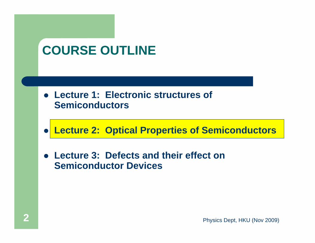
COURSE OUTLINE
Lecture 1: Electronic structures of Semiconductors
Lecture 2: Optical Properties of Semiconductors
Lecture 3: Defects and their effect on Semiconductor Devices

Physics Dept, HKU (Nov 2009)3
OPTICAL PROPERTIES OF SEMICONDUCTORS
OUTLINE– Optical Constants– Interband transitions & Critical Points– Exciton Effects– Quantum Confinement Effects on Optical
Properties– Polaritons
Physics Dept, HKU (Nov 2009)4
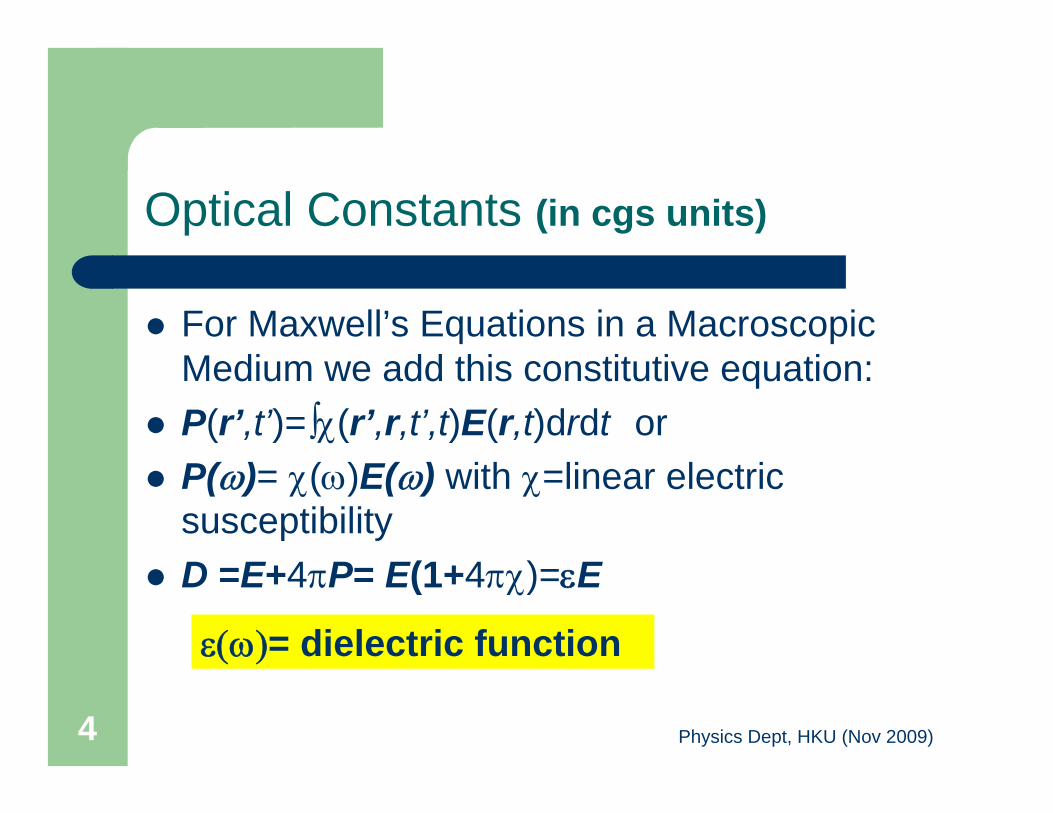
Optical Constants (in cgs units)
For Maxwell’s Equations in a Macroscopic Medium we add this constitutive equation:P(r’,t’)=∫χ(r’,r,t’,t)E(r,t)drdt orP(ω)= χ(ω)E(ω) with χ=linear electric susceptibilityD =E+4πP= E(1+4πχ)=εE
ε(ω)= dielectric function
Physics Dept, HKU (Nov 2009)5
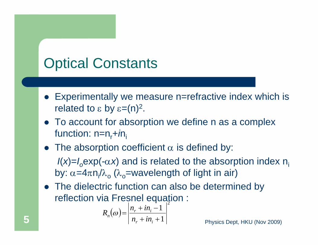
Optical Constants
Experimentally we measure n=refractive index which is related to ε by ε=(n)2.To account for absorption we define n as a complex function: n=nr+ini
The absorption coefficient α is defined by: I(x)=Ioexp(-αx) and is related to the absorption index niby: α=4πni/λo (λo=wavelength of light in air)The dielectric function can also be determined by reflection via Fresnel equation :
( )2
11++−+
=ir
irn inn
innR ω

Physics Dept, HKU (Nov 2009)6
Optical Constants of Si and GaAs[From Philipp & Ehrenreich 1967]
RR x 10
Si
0
20
40
60
80
R(%)
(a)
0
0-20
20
40
60
5 1510 20 250
0.5
1.0
1.5
2.0
Energy (eV)
-Im -1
-Im -1
i , ri
r
(b)
GaAs(a)
R x 10
R
0
20
40
60
R(%)
25
15
5
0
-5
0 5 10 15 20 25
0.4
0.8(b)
Energy (eV)
-Im -1
-Im -1r, i
i
rεr,εi
εr,εi
Imε-1
Imε-1
εr
εiImε-1

Physics Dept, HKU (Nov 2009)7
Imaginary Part of Dielectric Function of GaN (laser for blue-ray DVD)
Dielectric Function measured directly by method known as Ellipsometry
Physics Dept, HKU (Nov 2009)8
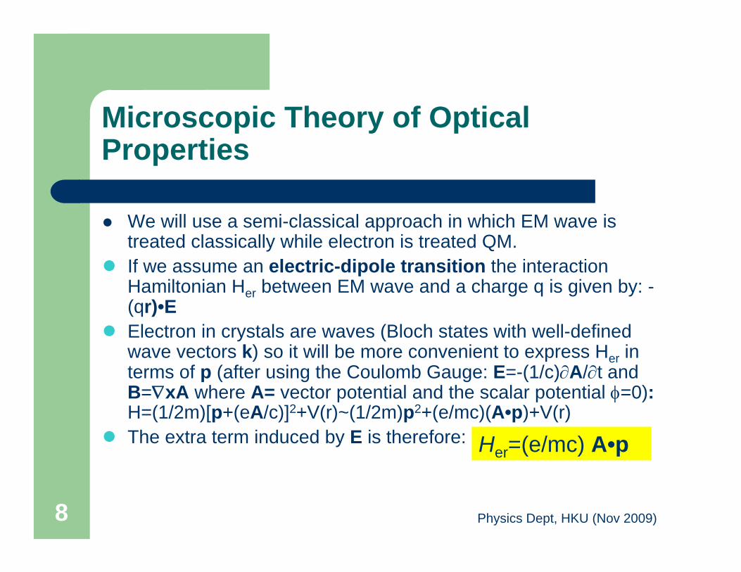
Microscopic Theory of Optical Properties
We will use a semi-classical approach in which EM wave is treated classically while electron is treated QM.If we assume an electric-dipole transition the interaction Hamiltonian Her between EM wave and a charge q is given by: -(qr)•EElectron in crystals are waves (Bloch states with well-defined wave vectors k) so it will be more convenient to express Her in terms of p (after using the Coulomb Gauge: E=-(1/c)∂A/∂t and B=∇xA where A= vector potential and the scalar potential φ=0): H=(1/2m)[p+(eA/c)]2+V(r)~(1/2m)p2+(e/mc)(A•p)+V(r)The extra term induced by E is therefore: Her=(e/mc) A•p

Physics Dept, HKU (Nov 2009)9
Microscopic Theory of Optical Properties
Using the Fermi Golden Rule the transition rate (per unit volume of crystal) from valence band to conduction band is given by:R=(2π/h)Σ|<c|Her|v>|2δ(Ec-Ev-hѡ)Where the matrix element can be shown to be approximated (for small k) by:
and |Pcv|2=|<c|p|v>|2.The final result is:
Physics Dept, HKU (Nov 2009)10
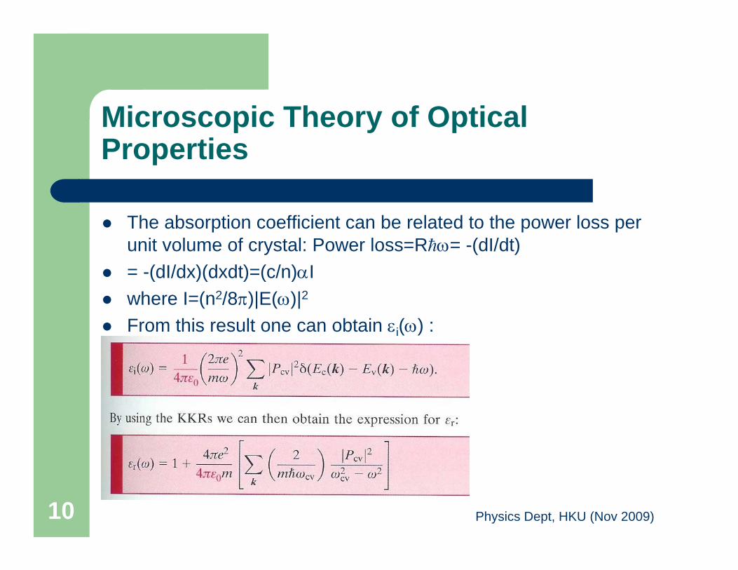
Microscopic Theory of Optical Properties
The absorption coefficient can be related to the power loss per unit volume of crystal: Power loss=Rhω= -(dI/dt)= -(dI/dx)(dxdt)=(c/n)αIwhere I=(n2/8π)|E(ω)|2
From this result one can obtain εi(ω) :
Physics Dept, HKU (Nov 2009)11
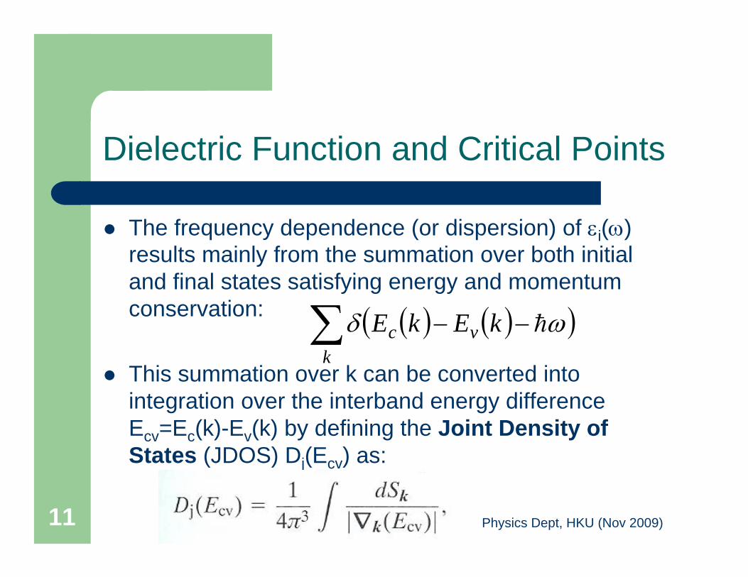
Dielectric Function and Critical Points
The frequency dependence (or dispersion) of εi(ω) results mainly from the summation over both initial and final states satisfying energy and momentum conservation:
This summation over k can be converted into integration over the interband energy difference Ecv=Ec(k)-Ev(k) by defining the Joint Density of States (JDOS) Dj(Ecv) as:
( ) ( )( )∑ −−k
vc kEkE ωδ h

Physics Dept, HKU (Nov 2009)12
Dielectric Function and Critical Points
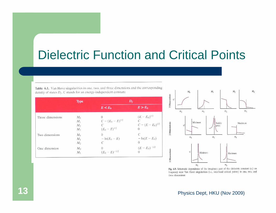
• Dj(Ecv) contains van Hove singularities whenever ∇k(Ecv)=0. The features, such as peaks and shoulders, in εi(ω) and εi(ω) are caused by these singularitiesThe type of singularities possible is strongly dependent on dimensionality
Physics Dept, HKU (Nov 2009)13
Dielectric Function and Critical Points

Physics Dept, HKU (Nov 2009)14
Dielectric Function and Critical Points
This band gap is a MoCP in 3D
This band gap is a M1CP in 3D but almost a Mo CP in 2D
Band Structure of Ge showing interbandtransitions labelled as Eo, E1 etc

Physics Dept, HKU (Nov 2009)15
Critical Points and the Absorption Spectrum of Ge
Agreement between Theory and Experiment is much better now
Lowest direct gap (Eo) of Ge
Physics Dept, HKU (Nov 2009)16
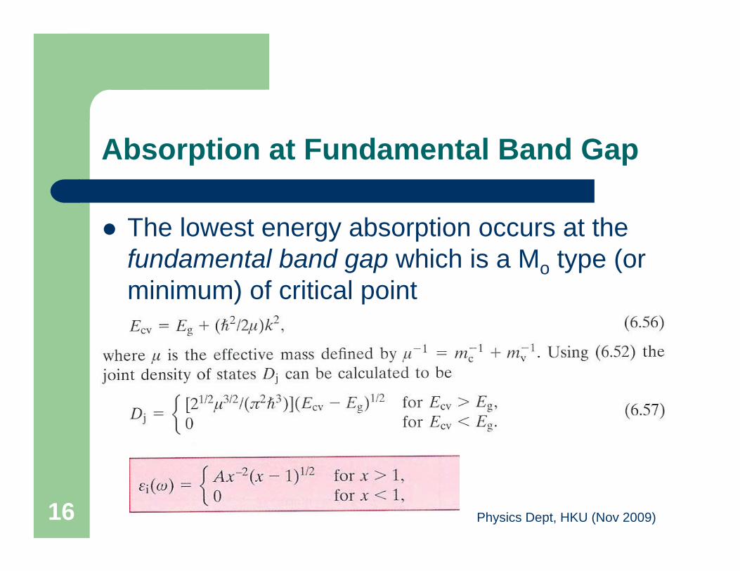
Absorption at Fundamental Band Gap
The lowest energy absorption occurs at the fundamental band gap which is a Mo type (or minimum) of critical point

Physics Dept, HKU (Nov 2009)17
Absorption at Fundamental Band Gap
Why at low T the absorption spectra of GaAs show peaks?

Physics Dept, HKU (Nov 2009)18
Correction to the One-Electron Picture
• When a photon excites an electron and hole pair there is a Coulomb attraction between the e and h (Final State Interaction) resulting in the formation of a two-particle bound state known as an exciton
• Exciton is neutral over all but carries an electric dipole moment. Exciton has been compared to a hydrogen atom or positronium. Actually exciton is more than just an “atom”. Since the electron and hole in the exciton are Bloch waves the exciton is a polarization wave.

Physics Dept, HKU (Nov 2009)19
Two pictures of the Excitation of Excitons
Exciton Wave functions and EnergyFrom Effective Mass Approximation:
Physics Dept, HKU (Nov 2009)20
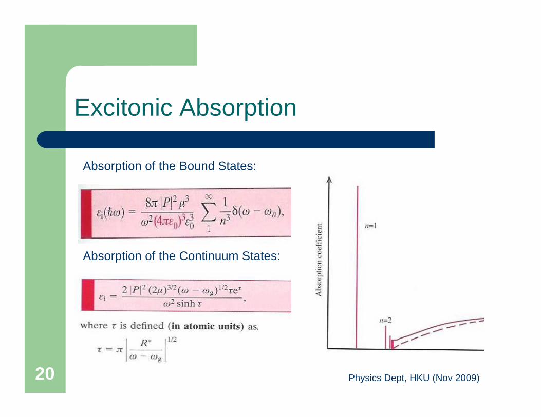
Excitonic Absorption
Absorption of the Bound States:
Absorption of the Continuum States:
Physics Dept, HKU (Nov 2009)21
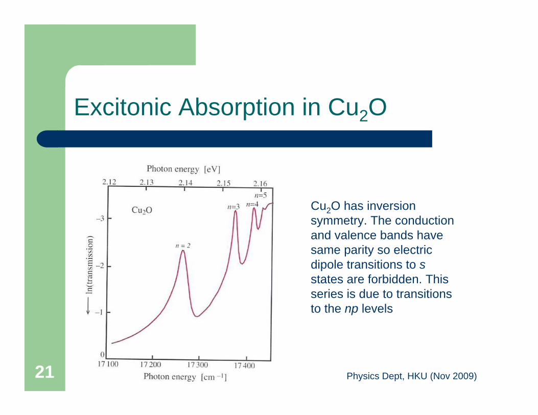
Excitonic Absorption in Cu2O
Cu2O has inversion symmetry. The conduction and valence bands have same parity so electric dipole transitions to sstates are forbidden. This series is due to transitions to the np levels

Physics Dept, HKU (Nov 2009)22
Enhancement of Electron-Radiation Interaction by Quantum Confinement
Absorption at exciton is enhanced into by Coulomb attraction between e and h. Absorption will also be enhanced if both e and h are physically confined together
Photon
Confined electron
Confined hole
Transition Probability~|<Φconduction|er•E|Φvalence>|2(|Ψ(0)|2)(JDOS)
Ψ is the envelope function and describes the overlap of the Electron and Hole wave functions. Confinement leads to increase in overlap of e and h wave functions

Physics Dept, HKU (Nov 2009)23
The QW Laser
A Laser utilizing Confinement of Carrierswith the additional benefit of Photon Confinement(An idea worth a Nobel Prize in Physics in 2000)
Physics Dept, HKU (Nov 2009)24
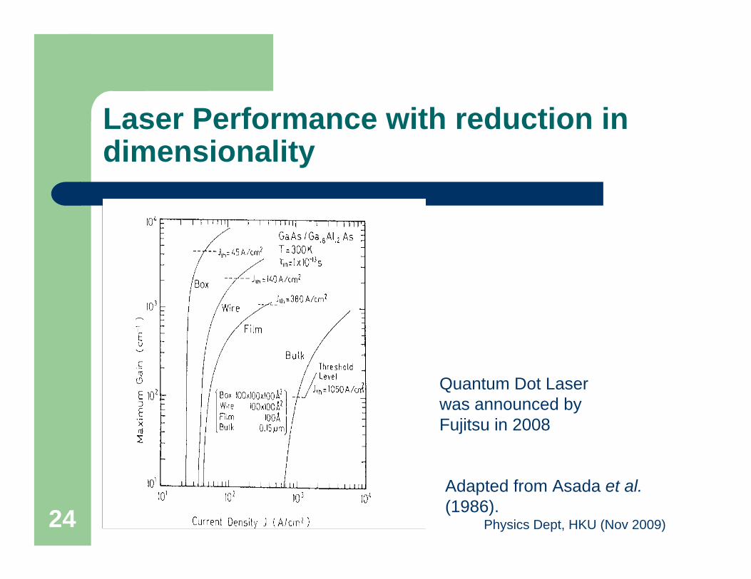
Laser Performance with reduction in dimensionality
Adapted from Asada et al.(1986).
Quantum Dot Laser was announced by Fujitsu in 2008
Physics Dept, HKU (Nov 2009)25
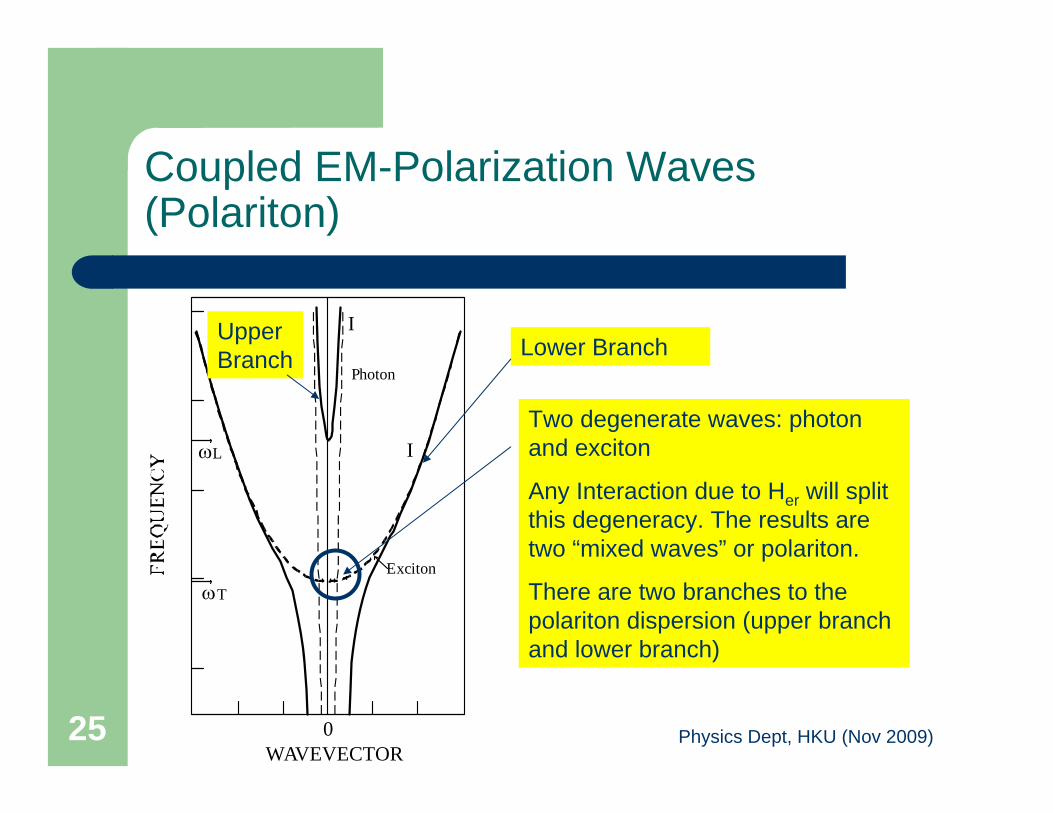
Coupled EM-Polarization Waves (Polariton)
Photon
Exciton
0
I
I
ωT
ωL
WAVEVECTOR
Two degenerate waves: photon and exciton
Any Interaction due to Her will split this degeneracy. The results are two “mixed waves” or polariton.
There are two branches to the polariton dispersion (upper branch and lower branch)
Lower BranchUpper Branch
Physics Dept, HKU (Nov 2009)26
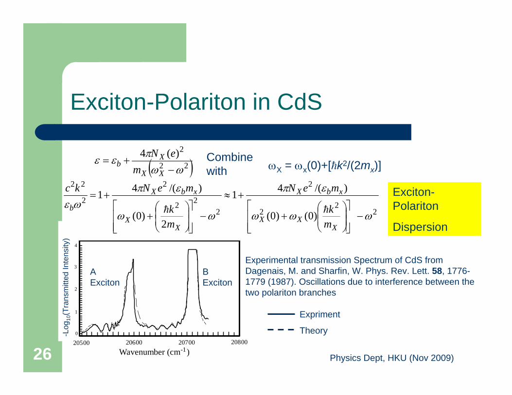
Exciton-Polariton in CdS
( )22
2)(4ωω
πεε−
+=XX
Xb m
eN
Wavenumber (cm )-120500 20600 20700 208000
1
2
3
4
ωX = ωx(0)+[hk2/(2mx)]
22
2
2
222
2
2
22
)0()0(
)/(41
2)0(
)/(41
ωωω
επ
ωω
επωε
−⎥⎥⎦
⎤
⎢⎢⎣
⎡⎟⎟⎠
⎞⎜⎜⎝
⎛+
+≈
−⎥⎥⎦
⎤
⎢⎢⎣
⎡⎟⎟⎠
⎞⎜⎜⎝
⎛+
+=
XXX
xbX
XX
xbX
b
mk
meN
mk
meNkc
hh
Combine with
Exciton-Polariton
Dispersion
Experimental transmission Spectrum of CdS from Dagenais, M. and Sharfin, W. Phys. Rev. Lett. 58, 1776-1779 (1987). Oscillations due to interference between the two polariton branches
Expriment
Theory
A Exciton
B Exciton
-Log
10(T
rans
mitt
ed In
tens
ity)
Physics Dept, HKU (Nov 2009)27
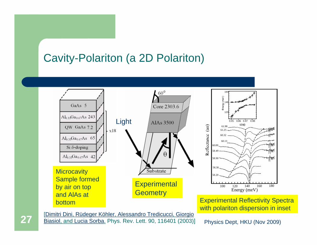
Cavity-Polariton (a 2D Polariton)
Energy (meV)100 120 140 160 180
58.20
58.38
58.90
58.49
60.0060.13
60.32
61.2561.98
0.85 0.86 0.87 0.88sinθ
120
140
160
MicrocavitySample formed by air on top and AlAs at bottom
Experimental Geometry
Experimental Reflectivity Spectra with polariton dispersion in inset
Light
[Dimitri Dini, Rüdeger Köhler, Alessandro Tredicucci, Giorgio Biasiol, and Lucia Sorba. Phys. Rev. Lett. 90, 116401 (2003)]
Physics Dept, HKU (Nov 2009)28
CONCLUSIONS
Semiconductors have many applications depending on their opticalproperties, such as lasers, LED, solar cells, image sensors etc.In the near infrared, visible and uv region the optical properties of semiconductors are determined by interband transitions between their valence band and conduction band.Coulomb attraction between e and h enhanced the absorption near the fundamental band gapQuantum confinement in QW will also enhance the emission probability between e and h leading to better lasersThe most fundamental approach to understand the optical properties of semiconductors is to consider polaritons.