advanced thin-film silicon solar cells
TRANSCRIPT
Miro ZemanDelft University of Technology, The Netherlands
Advanced Thin-Film Silicon Solar Cells
Acknowledgments:• Members of PVMD group at TUD• Nuon Helianthos, TU/e, UU, ECN, IPV Julich, OM&T, Ljubljana University• SenterNovem for financial support
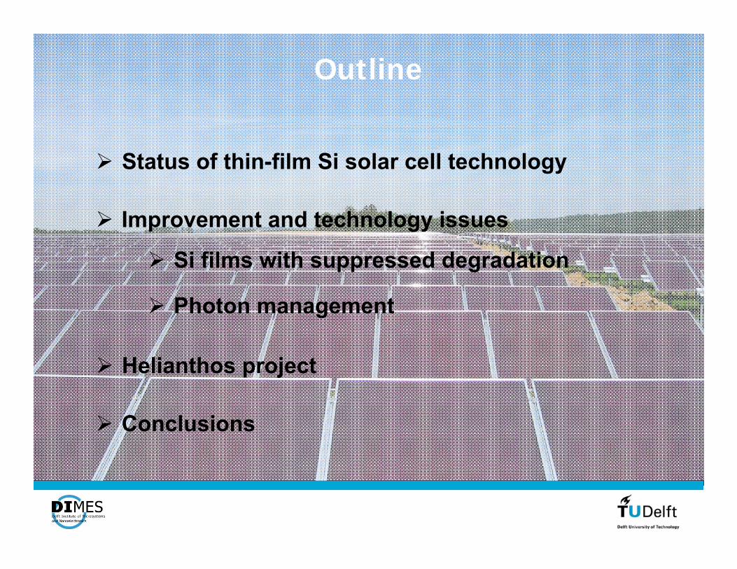
Outline
Helianthos project
Status of thin-film Si solar cell technology
Improvement and technology issues
Conclusions
Si films with suppressed degradation
Photon management
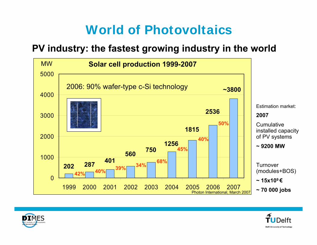
World of PhotovoltaicsPV industry: the fastest growing industry in the world
0
1000
2000
3000
4000
5000
1999 2000 2001 2002 2003 2004 2005 2006 2007
202 287 401560 750
1256
1815
~3800
MW Solar cell production 1999-2007
42% 40% 39% 34%68%
45%
50%
Photon International, March 2007
2006: 90% wafer-type c-Si technology
Estimation market:
2007Cumulative installed capacity of PV systems
~ 9200 MW
Turnover (modules+BOS)
~ 15x109 €~ 70 000 jobs
2536
40%

World of PhotovoltaicsPV industry: announced increase in capacity
0,0
5.000,0
10.000,0
15.000,0
20.000,0
25.000,0
30.000,0
35.000,0
40.000,0
45.000,0Pr
oduc
tion
Cap
acity
[MW
]
2006 2007 2008 2009 2010 2012
Crystalline SiliconThin Films
Arnulf Jäger-Waldau, EU-PVSEC-23, Valencia, 2008

Thin-Film PhotovoltaicsPV industry: announced increase in capacity
0
2.000
4.000
6.000
8.000
10.000
12.000
[MW
]
2006 2007 2008 2009 2010 2012
silicon basedCdTeCISDye + others
Oerlikon
Applied Materials
Arnulf Jäger-Waldau, EU-PVSEC-23, Valencia, 2008
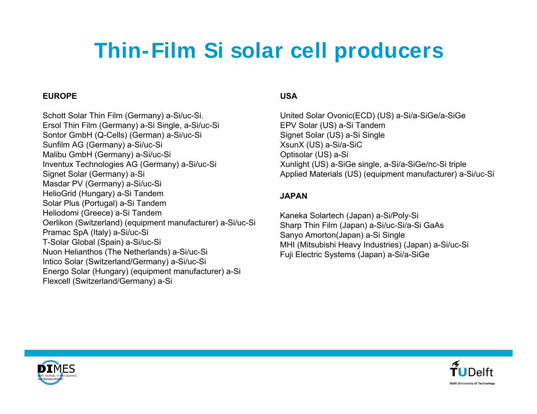
Thin-Film Si solar cell producers
EUROPE
Schott Solar Thin Film (Germany) a-Si/uc-Si.Ersol Thin Film (Germany) a-Si Single, a-Si/uc-SiSontor GmbH (Q-Cells) (German) a-Si/uc-SiSunfilm AG (Germany) a-Si/uc-SiMalibu GmbH (Germany) a-Si/uc-SiInventux Technologies AG (Germany) a-Si/uc-SiSignet Solar (Germany) a-SiMasdar PV (Germany) a-Si/uc-SiHelioGrid (Hungary) a-Si TandemSolar Plus (Portugal) a-Si TandemHeliodomi (Greece) a-Si TandemOerlikon (Switzerland) (equipment manufacturer) a-Si/uc-SiPramac SpA (Italy) a-Si/uc-SiT-Solar Global (Spain) a-Si/uc-SiNuon Helianthos (The Netherlands) a-Si/uc-SiIntico Solar (Switzerland/Germany) a-Si/uc-SiEnergo Solar (Hungary) (equipment manufacturer) a-SiFlexcell (Switzerland/Germany) a-Si
USA
United Solar Ovonic(ECD) (US) a-Si/a-SiGe/a-SiGeEPV Solar (US) a-Si TandemSignet Solar (US) a-Si SingleXsunX (US) a-Si/a-SiCOptisolar (US) a-SiXunlight (US) a-SiGe single, a-Si/a-SiGe/nc-Si tripleApplied Materials (US) (equipment manufacturer) a-Si/uc-Si
JAPAN
Kaneka Solartech (Japan) a-Si/Poly-SiSharp Thin Film (Japan) a-Si/uc-Si/a-Si GaAsSanyo Amorton(Japan) a-Si SingleMHI (Mitsubishi Heavy Industries) (Japan) a-Si/uc-SiFuji Electric Systems (Japan) a-Si/a-SiGe

CHINA
Topray Solar(Shenzhen China) a-Si TandemSoltechpv (Beijing China) a-Si TandemJinneng Solar (Tianjin China) a-Si TandemPolar PV (Anhui China) a-Si Single, TandemTrony (Shenzhen China) a-Si SingleSumoncle (Shenzhen China) a-Si Singlehksolar (Harbin China) a-Si SingleXinao Group (Hebe China) a-Si TandemSuntech (Shanghai China) a-Si/uc-SiBSTRPV (Weihan China) a-Si TandemChina Solar Power (Yantai China) a-Si SingleQS Solar (Nantong China) a-Si TandemYuanchang (Changzhou China) a-Si TandemGanneng Huaji (Jiangxi China) a-Si TandemGS Solar (Quanzhou China) a-Si TandemZhongshang Quanxin (Zhongshan China) a-Si TandemCineng PV (Hangzhou China) a-Si TandemShenyang Hanfeng (Shenyang China) a-Si TandemUni-Solar Jinneng (Tianjin China) a-Si/a-SiGe/a-SiGe
Thin-Film Si solar cell producers
TAIWAN
Green Energy Technology (Taoyuan Taiwan) a-Si SingleCMC (Taoyuan Taiwan) a-Si SingleYutong Light Energy (Tainan Taiwan) a-Si/uc-SiNexpower (Central Taiwan) a-Si SingleSunner Solar (Central Taiwan) a-Si SingleFormosun (Hsinchu Taiwan) a-Si TandemKenmos PV (Tainan Taiwan) a-Si TandemNanoWin (Tainan Taiwan) a-Si/uc-SiSinonar (Hsinchu Taiwan) a-Si Tandem
OTHER
Bangkok Solar (Thailand) a-Si TandemSolarMorph (Singapore) a-Si/uc-SiMoser Baer Photo Voltaic (India) a-Si SingleLambda Energia (Mexico) a-Si/a-SiC
In 2008 more than 60 companies

Strategic Research Agenda: EU roadmap
www.eupvplatform.org
Wim Sinke (ECN, Leader of WG 3 : Science, technology & applications of EU PV Technology Platform)

Current developments:• increase in TF Si solar-cell production (in 2010 ~ 8 GW capacity)• complete production lines available
Future developments:• short term: optimize tandem cell• long term: optimize triple cell, breakthrough concepts for high
efficiency (η>17%)
Thin-film Si solar cell technologyPresent status:+ Promising low-cost solar cell technology+ Industrial production experience (Flat panel display industry)- Relatively low stabilized efficiencies (η ≈6-7%)+ Double-junction micromorph solar cell (η>10%)
• ideal combination of materials (a-Si:H/μc-Si:H) for converting AM1.5 solar spectrum into electricity

Thin-film Si solar cell technology
Thin-film Si solar cells on glass
Power plant
Roof integration and new designs
Thin-film Si solar cell technology
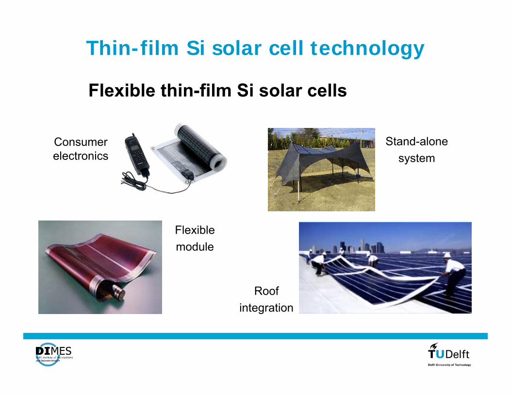
Flexible thin-film Si solar cells
Roof integration
Consumer electronics
Stand-alonesystem
Flexible module

Thin-film Si solar cell technology
+-
p-typesc Si
Al
p++
Al Al
SiO2
n+
p++
c-Si (200-300 μm)
Thin film Si (0.3 - 5 μm)
•• Material usage Material usage strongly reducedstrongly reduced
•• Energy and cost Energy and cost strongly reducedstrongly reduced
Glass superstrate
TCO
p-type
Intrinsic a-Si:H
n-typeMetal electrode
+ -
a-Si:H (0.3-0.5 μm)

Thin-film Si solar cell technology
Gas system rf generator
electrode
electrode
substrate
heater
Pump system
reaction chamber
plasma
Plasma Enhanced CVD
+ Low deposition temperature+ Use of cheap substrates+ Large area deposition+ Easy doping and alloying
– Low deposition rate (1-2 Å/s)
High potential for low cost solar cells
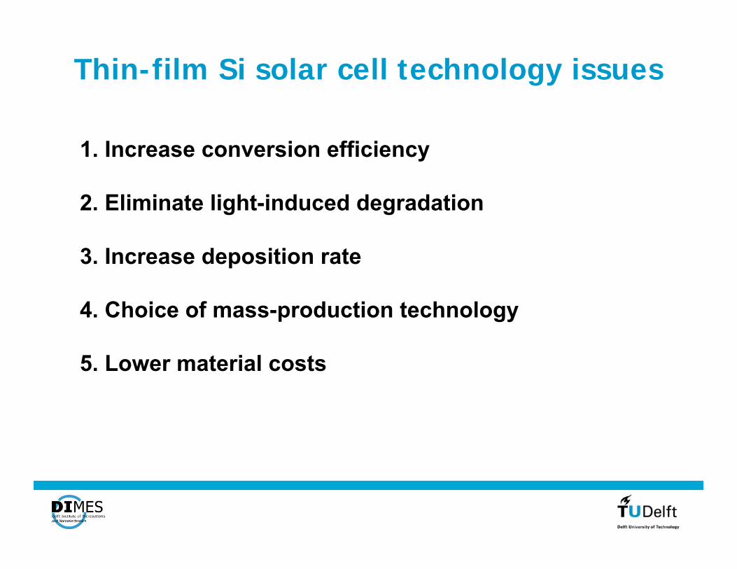
Thin-film Si solar cell technology issues
1. Increase conversion efficiency
2. Eliminate light-induced degradation
3. Increase deposition rate
4. Choice of mass-production technology
5. Lower material costs

Single-junction a-Si:H solar cells:
Thin-film Si solar cell technology
Absorption of light• surface texture of the TCOs• ZnO back reflector
Extraction of the charge carriers• TCO/p interface• p-type window layer• p/i hetero-junction interface• quality of the intrinsic layer
Crucial parts of a-Si:H solar cell:
First a-Si solar cell made in 1974 by David Carlson.
-20
-15
-10
-5
0
5
-0.2 0.0 0.2 0.4 0.6 0.8 1.0Voltage [V]
Cur
rent
den
sity
[mA
cm-2]
initial
degraded
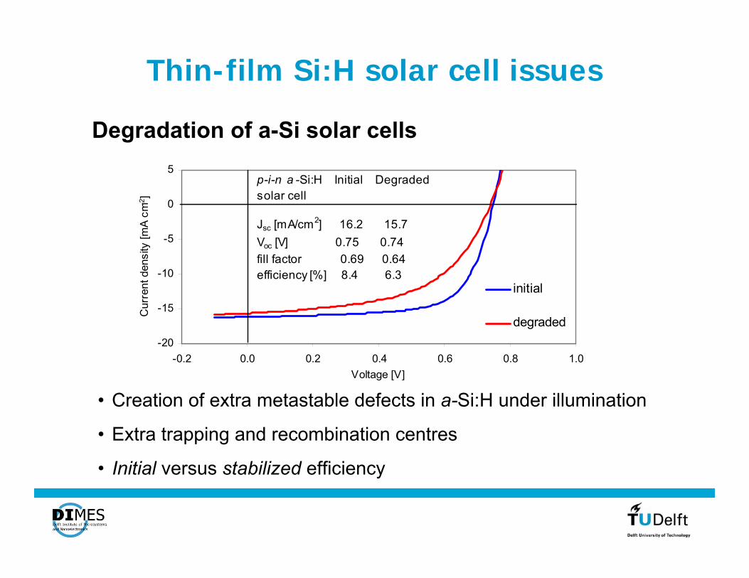
p-i-n a -Si:H Initial Degradedsolar cell
Jsc [mA/cm2] 16.2 15.7Voc [V] 0.75 0.74fill factor 0.69 0.64efficiency [%] 8.4 6.3
• Creation of extra metastable defects in a-Si:H under illumination
• Extra trapping and recombination centres
• Initial versus stabilized efficiency
Thin-film Si:H solar cell issues
Degradation of a-Si solar cells

Thin-film Si:H solar cells challenges
Increasing efficiency
Photon management• Textured substrates - scattering• Back reflector• Novel approaches
Multi-bandgap concept• Low band-gap materials
Suppressing degradation
Stable material• pc-Si:H, μc-Si:H or poly c-Si• New deposition techniques• Hydrogen diluted silane
Multi-junction concept• Tandem solar cells

300 500 700 900 1100 1300 1500Wavelength [nm]
Pho
ton
flux
[1027
ph
/ m3 s
]
4.13 2.48 1.77 1.38 1.13 0.95 0.83
Photon energy [eV]
5.0
4.0
3.0
2.0
1.0
0.0
a-Si a-SiGe
AM1.5 global solar spectrum
Increase efficiency
Multi-bandgap solar cell concept
Efficient use of solar spectrum
EFEner
gy
p ni
a-Si
EF
p ni
a-Si
EF
p nin pi
a-Si a-Si
Multi-junction solar cell concept
EF
p nin p
a-Si
i
a-SiGe or μc-Si
Suppress degradation
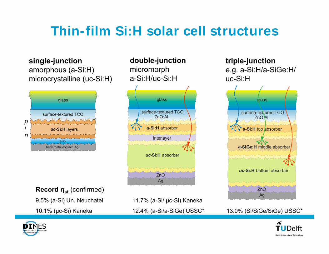
Thin-film Si:H solar cell structures
uc-Si:H bottom absorber
Ag ZnO
surface textured - TCOZnO:Al
glass
a-Si:H top absorber
a-Si :HGe middle absorber
surface textured TCO-
uc-Si:H absorber
Ag ZnO
surface textured - TCOZnO:Al
glass
a-Si:H absorber
interlayer
surface textured TCO-
glass
uc-Si:H layers
back metal contact (Ag)
pin
ZnO
single-junctionamorphous (a-Si:H)microcrystalline (uc-Si:H)
double-junctionmicromorpha-Si:H/uc-Si:H
triple-junctione.g. a-Si:H/a-SiGe:H/uc-Si:H
Record ηst (confirmed) 9.5% (a-Si) Un. Neuchatel
10.1% (μc-Si) Kaneka
11.7% (a-Si/ μc-Si) Kaneka
12.4% (a-Si/a-SiGe) USSC* 13.0% (Si/SiGe/SiGe) USSC*

Proto-crystalline Si growth regime:• Effect of high H dilution of silane, dilution ratio R=[H2]/[SiH4]
Si:H films from hydrogen diluted silane

Si:H films from hydrogen diluted silane
Proto-crystalline Si growth regime:Glass substrate
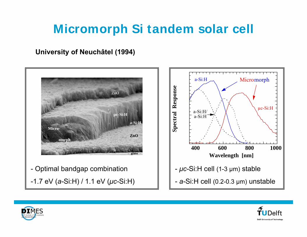
Micromorph Si tandem solar cell
University of Neuchâtel (1994)
ZnO
µc-Si:H
a-Si:H
ZnO
glass
Micro-
morph
- Optimal bandgap combination
-1.7 eV (a-Si:H) / 1.1 eV (μc-Si:H)
400 600 800 1000
Spec
tral
Res
pons
e
Wavelength [nm]
morph
a-Si:H/a-Si:H
Microa-Si:H
µc-Si:H
- μc-Si:H cell (1-3 μm) stable
- a-Si:H cell (0.2-0.3 μm) unstable
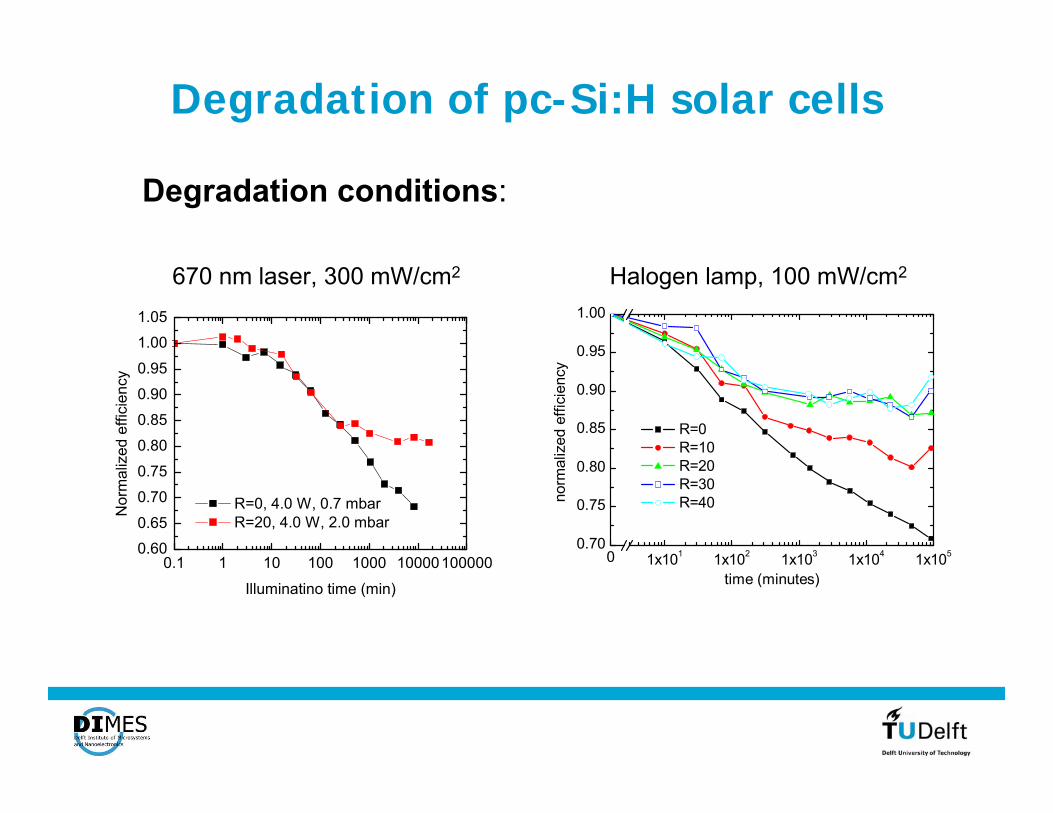
Degradation of pc-Si:H solar cells
Degradation conditions:
0.1 1 10 100 1000 100001000000.60
0.65
0.70
0.75
0.80
0.85
0.90
0.95
1.00
1.05
Nor
mal
ized
effi
cien
cy
Illuminatino time (min)
R=0, 4.0 W, 0.7 mbar R=20, 4.0 W, 2.0 mbar
0 1x101 1x10² 1x10³ 1x10⁴ 1x1050.70
0.75
0.80
0.85
0.90
0.95
1.00
norm
aliz
ed e
ffici
ency
time (minutes)
R=0 R=10 R=20 R=30 R=40
670 nm laser, 300 mW/cm2 Halogen lamp, 100 mW/cm2

Photon management
Proper handling of incident photons which have to
be trapped and absorbed in the absorber layers
of a solar cell

Photon management
Light trapping techniques:• Manipulation of light propagation: multiple passes
Engineering of optically-active layers(back and intermediate reflectors, layers for optical matching)
• Light scattering: change direction of propagation
Design of surface texture (random or periodically textured surfaces)
Trap photons in the absorber layer and enlarge their average path

Modeling of thin-film Si solar cells
Optical modeling:• Increase photocurrent
Understand light trapping
Evaluate optical losses
Design efficient light-trapping schemes
Integrated optical nad electrical modeling:• Increase Voc and FF
Evaluate recombination losses
Design material and interface properties
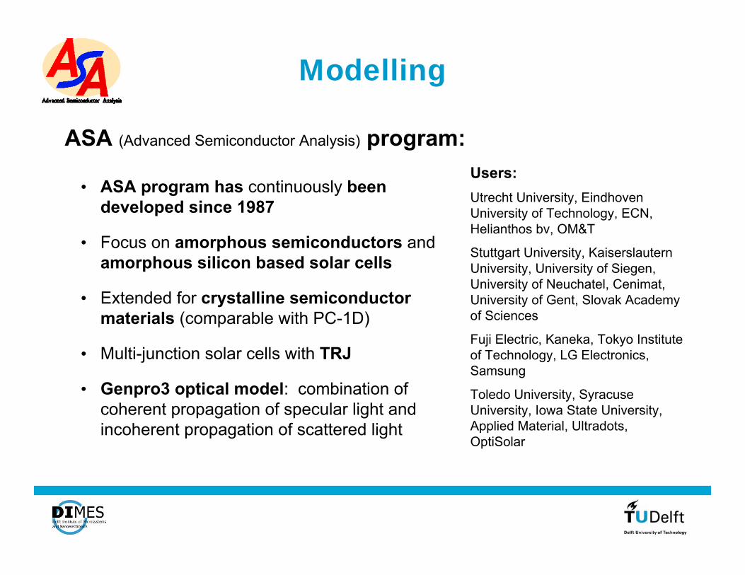
ASA (Advanced Semiconductor Analysis) program: Users:Utrecht University, Eindhoven University of Technology, ECN, Helianthos bv, OM&T
Stuttgart University, Kaiserslautern University, University of Siegen, University of Neuchatel, Cenimat, University of Gent, Slovak Academy of Sciences
Fuji Electric, Kaneka, Tokyo Institute of Technology, LG Electronics, Samsung
Toledo University, Syracuse University, Iowa State University, Applied Material, Ultradots, OptiSolar
Modelling
• ASA program has continuously been developed since 1987
• Focus on amorphous semiconductors andamorphous silicon based solar cells
• Extended for crystalline semiconductor materials (comparable with PC-1D)
• Multi-junction solar cells with TRJ
• Genpro3 optical model: combination of coherent propagation of specular light and incoherent propagation of scattered light
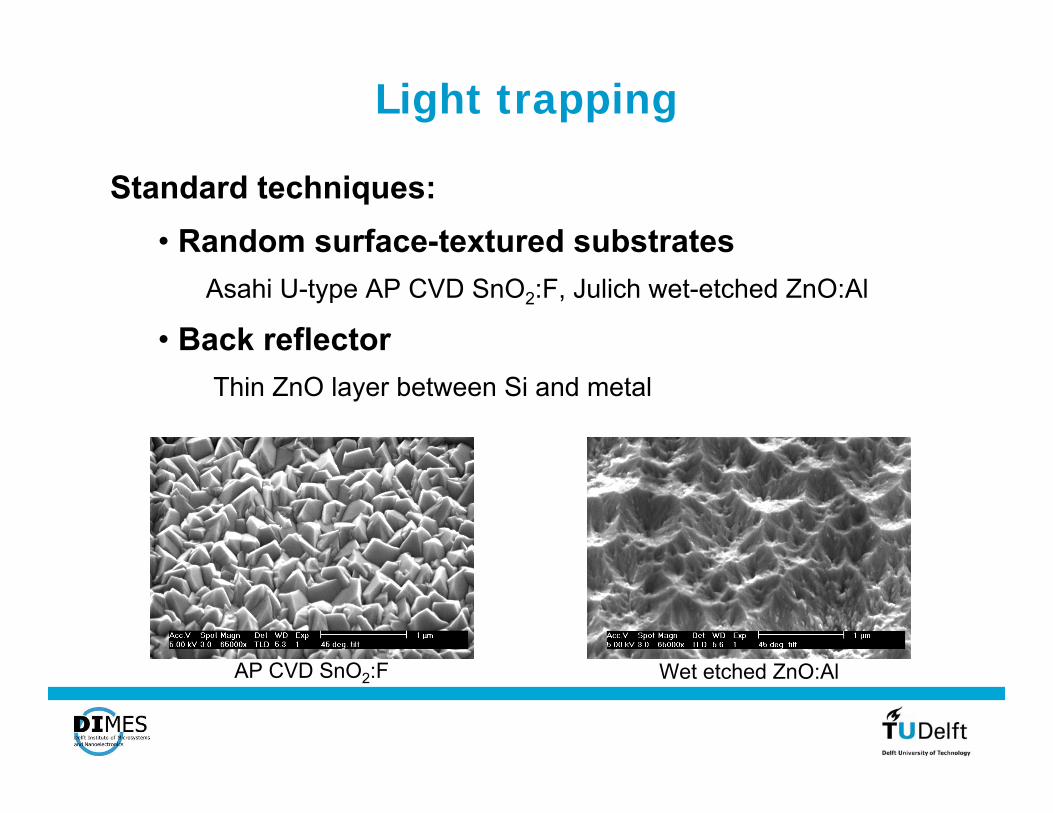
Light trapping
AP CVD SnO2:F Wet etched ZnO:Al
Standard techniques:• Random surface-textured substrates
Asahi U-type AP CVD SnO2:F, Julich wet-etched ZnO:Al
• Back reflectorThin ZnO layer between Si and metal
Light trapping
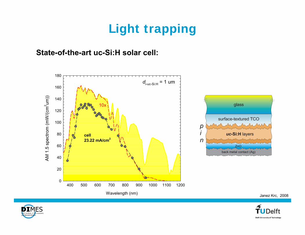
State-of-the-art uc-Si:H solar cell:
Wavelength (nm)
400 500 600 700 800 900 1000 1100 1200
AM
1.5
spe
ctro
m (m
W/(c
m2 um
))
0
20
40
60
80
100
120
140
160
180
di-uc-Si:H = 1 um
cell23.22 mA/cm2
10x
surface textured TCO-
glass
uc-Si:H layers
back metal contact (Ag)
pin
ZnO
Janez Krc, 2008
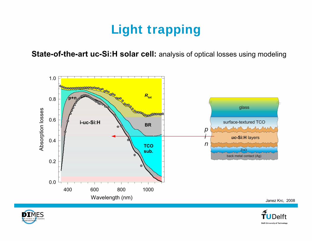
Wavelength (nm)400 600 800 1000
Abs
orpt
ion
loss
es
0.0
0.2
0.4
0.6
0.8
1.0
Rtot
BR
TCOsub.
i-uc-Si:H
p+n
Light trapping
surface textured TCO-
glass
uc-Si:H layers
back metal contact (Ag)
pin
ZnO
State-of-the-art uc-Si:H solar cell: analysis of optical losses using modeling
Janez Krc, 2008

Improving device performance
200 nm
2.2 um
Wavelength, λ (nm)400 600 800 1000
Qua
ntum
Effi
cien
cy, Q
E
0.0
0.2
0.4
0.6
0.8
1.0
QEtop QEbot
Rtot
10.0 mA/cm2 14.3 mA/cm2
Starting
Modelling of a-Si:H/μc-Si:H solar cells:
(ZnO)
M. Zeman and J. Krc, Optical and electrical modeling of thin-film silicon solar cells, J. Mater. Res., 23 (4), Apr 2008
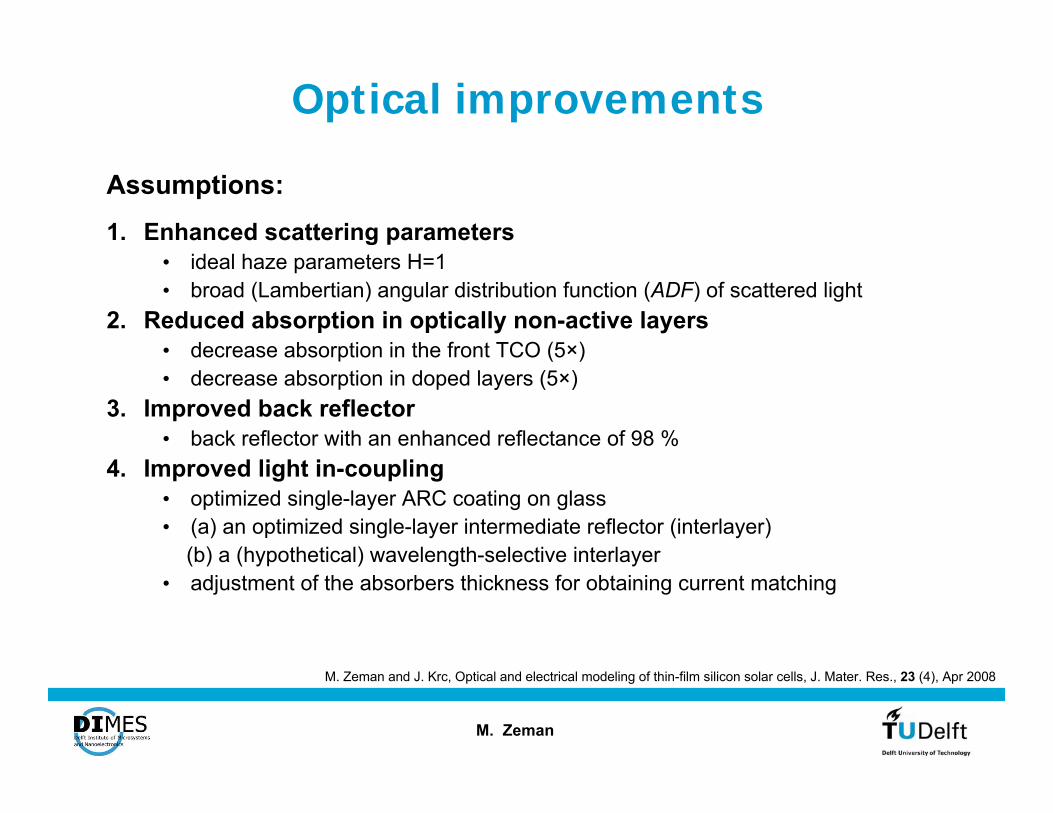
Assumptions:
1. Enhanced scattering parameters• ideal haze parameters H=1• broad (Lambertian) angular distribution function (ADF) of scattered light
2. Reduced absorption in optically non-active layers• decrease absorption in the front TCO (5×)• decrease absorption in doped layers (5×)
3. Improved back reflector• back reflector with an enhanced reflectance of 98 %
4. Improved light in-coupling• optimized single-layer ARC coating on glass• (a) an optimized single-layer intermediate reflector (interlayer)
(b) a (hypothetical) wavelength-selective interlayer• adjustment of the absorbers thickness for obtaining current matching
M. Zeman
Optical improvements
M. Zeman and J. Krc, Optical and electrical modeling of thin-film silicon solar cells, J. Mater. Res., 23 (4), Apr 2008

Scattering angle, ϕ, (degrees)-90 -60 -30 0 30 60 90
AD
F T
0.0
0.2
0.4
0.6
0.8
1.0
σrms = 60 nm
Lambertian
ZnOetched
W a ve le n g th , λ (n m )60 0 70 0 80 0 9 0 0 1 00 0 1 10 0
Ref
lect
ance
, R (%
)8 0
85
90
95
1 00
ro ug h Z n O /A g
98 %
Lambertian angular distribution(cos) function of scattered light
Improved back reflector R=98%(distributed Bragg reflectors)
M. Zeman and J. Krc, Optical and electrical modeling of thin-film silicon solar cells, J. Mater. Res., 23 (4), Apr 2008
Optical improvements

Wavelength, λ (nm)400 600 800 1000
Qua
ntum
Effi
cien
cy, Q
E
0.0
0.2
0.4
0.6
0.8
1.0
QEtop QEbot
Rtot
15.65 mA/cm2 16.48 mA/cm2
Improved
200 nm
2.2 um
(ZnO)
Modelling of a-Si:H/μc-Si:H solar cells:
Improving device performance
M. Zeman and J. Krc, Optical and electrical modeling of thin-film silicon solar cells, J. Mater. Res., 23 (4), Apr 2008
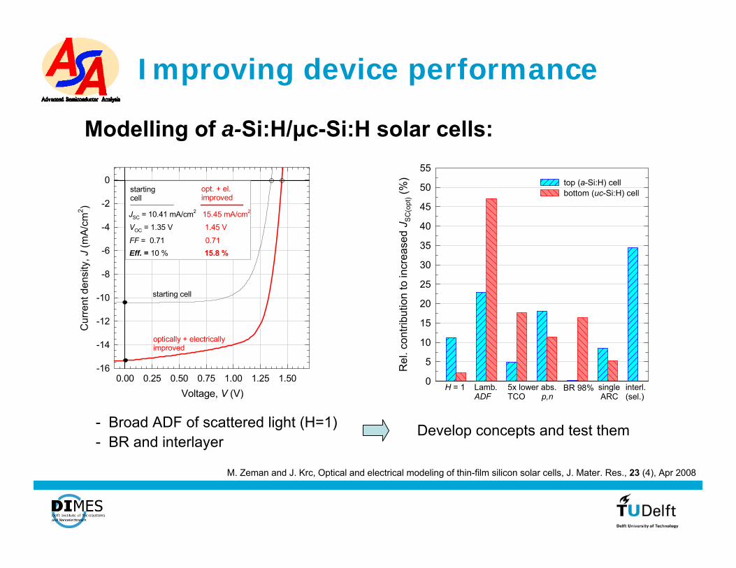
Rel
. con
tribu
tion
to in
crea
sed
J SC
(opt
) (%
)
0
5
10
15
20
25
30
35
40
45
50
55top (a-Si:H) cellbottom (uc-Si:H) cell
BR 98%5x lower abs.TCO p,n
H = 1 Lamb.ADF
single ARC
interl.(sel.)
- Broad ADF of scattered light (H=1)- BR and interlayer
Voltage, V (V)0.00 0.25 0.50 0.75 1.00 1.25 1.50
Cur
rent
den
sity
, J (m
A/c
m2 )
-16
-14
-12
-10
-8
-6
-4
-2
0
JSC = 10.41 mA/cm2 15.45 mA/cm2
VOC = 1.35 V 1.45 V
FF = 0.71 0.71Eff. = 10 % 15.8 %
starting cell
opt. + el.improved
starting cell
optically + electricallyimproved
Develop concepts and test them
Modelling of a-Si:H/μc-Si:H solar cells:
Improving device performance
M. Zeman and J. Krc, Optical and electrical modeling of thin-film silicon solar cells, J. Mater. Res., 23 (4), Apr 2008

Light-In projectTUD, Helianthos
ECN, OM&T
• Wavelength-selective manipulation of reflection and transmission of light at interfaces using 1-D photonic crystals
• Concept of modulated 1-D photonic crystals
• Applied as back and intermediate reflectors
Advanced concepts for light trapping
Wavelength (nm)600 800 1000 1200 1400
Ref
lect
ance
0.0
0.2
0.4
0.6
0.8
1.0 100 %
PC_1
50/100 nm
Wavelength (nm)
600 800 1000 1200 1400
Ref
lect
ance
0.0
0.2
0.4
0.6
0.8
1.0 100 %
PC_2
70/140 nm

Light-In projectTUD, Helianthos
ECN, OM&T
• Angle-selective manipulation of light scattered at the rough interfaces using 1-D and 2-D diffraction gratings
Scattering angle (ϕscatt)
-90 -60 -30 0 30 60 90
AD
F T (a.
u.)
0.0
0.2
0.4
0.6
0.8
1.0
P = 700 nmh = 80 nm
Asahi U-type
ϕinc = 0o
ZnO:Al(40" etched)σr � 110 nm
Advanced concepts for light trapping

0 50 100 150 200 250 3007.4
7.6
7.8
8.0
8.2
8.4
8.6
8.8
9.0
Period = 600 nm
Asahi reference
Ave
rage
Effi
cien
cy (%
)
Feature height (nm)
Light-In projectTUD, Helianthos
ECN, OM&T
Average efficiency of 10 best cells plotted versus groove height
Advanced concepts for light trapping
• Angle-selective manipulation of light scattered at the rough interfaces using 1-D diffraction gratings

Light-In projectTUD, Helianthos
ECN, OM&T
0 50 100 150 200 250 3007.47.67.88.08.28.48.68.89.09.29.4
Period = 600 nm 2D period = 500-800 nm
Asahi reference
Ave
rage
Effi
cien
cy (%
)
Feature height (nm)
Advanced concepts for light trapping
• Angle-selective manipulation of light scattered at the rough interfaces using 2-D diffraction gratings
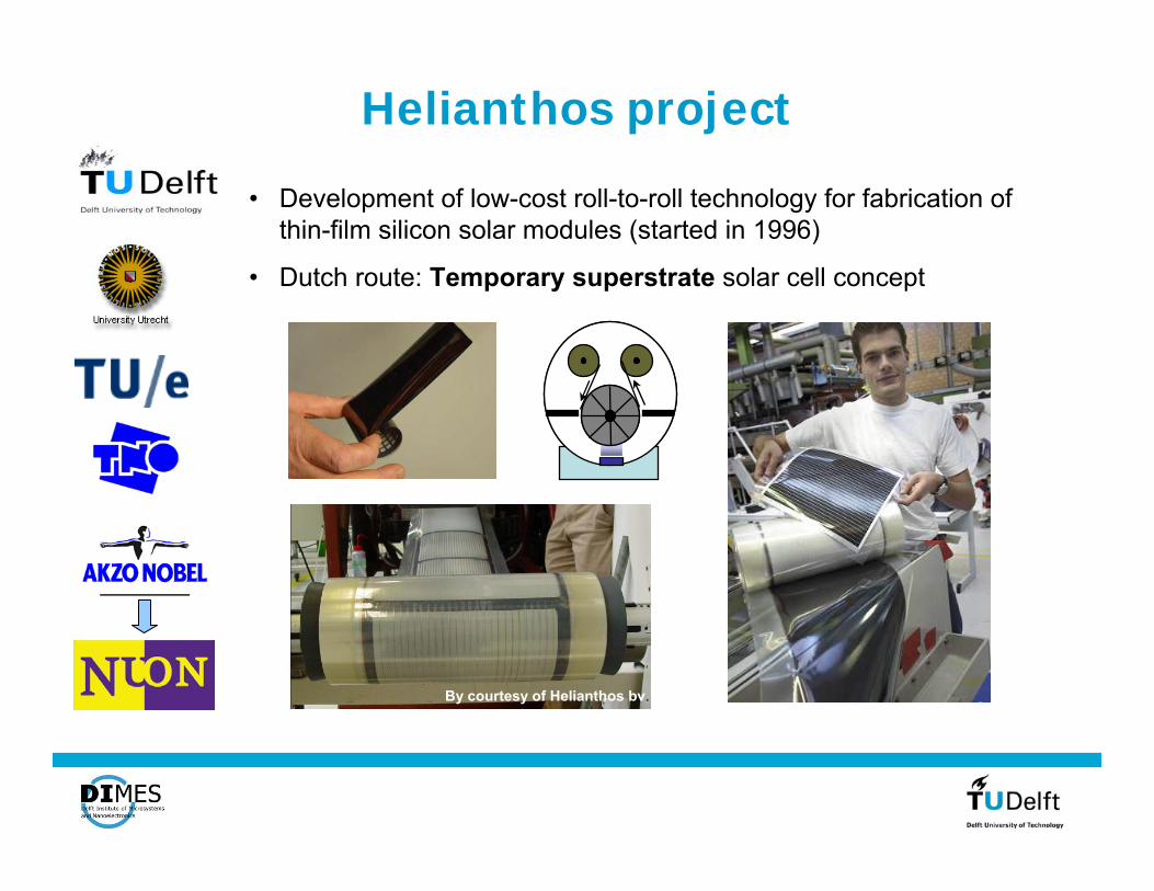
Helianthos project
• Development of low-cost roll-to-roll technology for fabrication of thin-film silicon solar modules (started in 1996)
• Dutch route: Temporary superstrate solar cell concept
By courtesy of Helianthos bv.
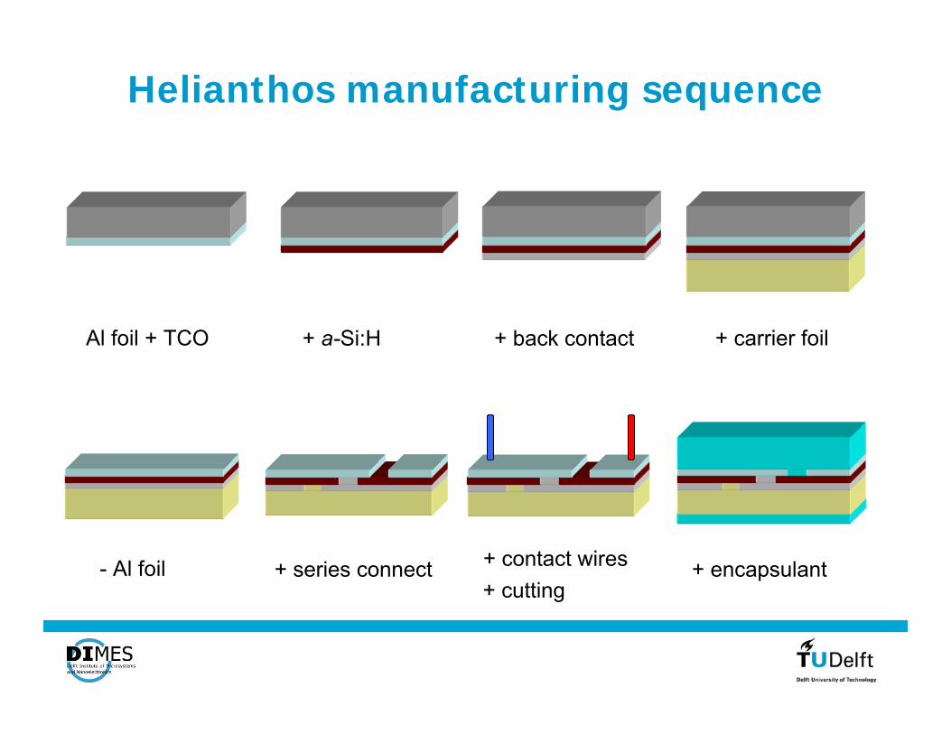
Helianthos manufacturing sequence
- Al foil
Al foil + TCO + a-Si:H + back contact + carrier foil
+ series connect + contact wires+ cutting
+ encapsulant
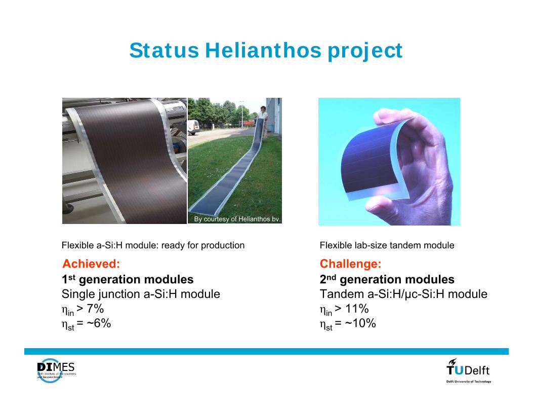
Status Helianthos project
Flexible lab-size tandem moduleFlexible a-Si:H module: ready for production
1st generation modulesSingle junction a-Si:H module ηin > 7%ηst = ~6%
2nd generation modulesTandem a-Si:H/μc-Si:H module ηin > 11%ηst = ~10%
Achieved: Challenge:
By courtesy of Helianthos bv.
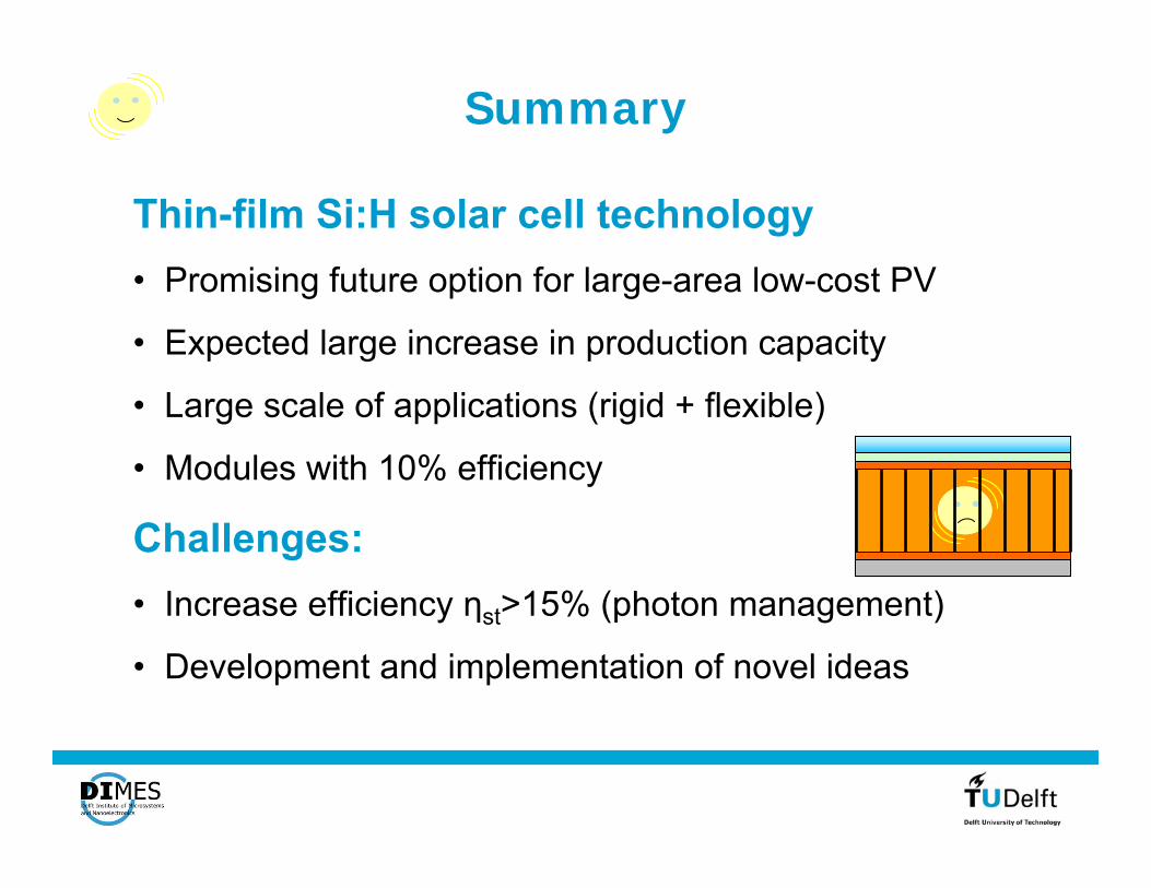
Summary
Thin-film Si:H solar cell technology• Promising future option for large-area low-cost PV
• Expected large increase in production capacity
• Large scale of applications (rigid + flexible)
• Modules with 10% efficiency
Challenges:• Increase efficiency ηst>15% (photon management)
• Development and implementation of novel ideas