adv7343 daughter card - support - spectrum digital inc
TRANSCRIPT

ADV7343 Daughter Card forDM6467 HD 1080P EVM
2009 DSP Development Systems
ReferenceTechnical

ADV7343 Daughter Card for DM6467 HD 1080P EVM
Technical Reference
512085-0001 Rev. ANovember 2009
SPECTRUM DIGITAL, INC.12502 Exchange Drive, Suite 440 Stafford, TX. 77477
Tel: 281.494.4505 Fax: [email protected] www.spectrumdigital.com

IMPORTANT NOTICE
Spectrum Digital, Inc. reserves the right to make changes to its products or to discontinue anyproduct or service without notice. Customers are advised to obtain the latest version of relevantinformation to verify that the data being relied on is current before placing orders.
Spectrum Digital, Inc. warrants performance of its products and related software to currentspecifications in accordance with Spectrum Digital’s standard warranty. Testing and other qualitycontrol techniques are utilized to the extent deemed necessary to support this warranty.
Please be aware that the products described herein are not intended for use in life-support appliances, devices, or systems. Spectrum Digital does not warrant nor is Spectrum Digital liable for the product described herein to be used in other than a development environment.
Spectrum Digital, Inc. assumes no liability for applications assistance, customer product design, software performance, or infringement of patents or services described herein. Nor does SpectrumDigital warrant or represent any license, either express or implied, is granted under any patent right,copyright, or other intellectual property right of Spectrum Digital, Inc. covering or relating to anycombination, machine, or process in which such Digital Signal Processing development products orservices might be or are used.
WARNING
This equipment is intended for use in a laboratory test environment only. It generates, uses, and canradiate radio frequency energy and has not been tested for compliance with the limits of computingdevices pursuant to subpart J of part 15 of FCC rules, which are designed to provide reasonableprotection against radio frequency interference. Operation of this equipment in other environmentsmay cause interference with radio communications, in which case the user at his own expense will berequired to take whatever measures necessary to correct this interference.
Copyright © 2009 Spectrum Digital, Inc.

Contents
1 Introduction to the ADV7343 Daughter Card . . . . . . . . . . . . . . . . . . . . . . . . . . . . . . . . . . 1-1 Provides you with a description of the ADV7343 Daughter Card, key features, and block diagram. 1.1 Key Features . . . . . . . . . . . . . . . . . . . . . . . . . . . . . . . . . . . . . . . . . . . . . . . . . . . . . . . . . . 1-2 1.2 ADV7343 Daughter Card Installation . . . . . . . . . . . . . . . . . . . . . . . . . . . . . . . . . . 1-42 Physical Specifications . . . . . . . . . . . . . . . . . . . . . . . . . . . . . . . . . . . . . . . . . . . . . . . . . . . . . 3-1 Describes the physical layout of the ADV7343 Daughter Card and its interfaces. 2.1 Board Layout . . . . . . . . . . . . . . . . . . . . . . . . . . . . . . . . . . . . . . . . . . . . . . . . . . . . . . . . 2-2 2.2 Connectors . . . . . . . . . . . . . . . . . . . . . . . . . . . . . . . . . . . . . . . . . . . . . . . . . . . . . . . . 2-3 2.2.1 J1, Composite Video . . . . . . . . . . . . . . . . . . . . . . . . . . . . . . . . . . . . . . . . . . . . . . . . . 2-3 2.2.2 J2, Pb Video Output . . . . . . . . . . . . . . . . . . . . . . . . . . . . . . . . . . . . . . . . . . . . . . . . . 2-3 2.2.3 J3, Pr Video Output . . . . . . . . . . . . . . . . . . . . . . . . . . . . . . . . . . . . . . . . . . . . . . . . . 2-4 2.2.4 J4, Y Video Output . . . . . . . . . . . . . . . . . . . . . . . . . . . . . . . . . . . . . . . . . . . . . . . . . 2-4 2.2.5 P1, S-Video Connector . . . . . . . . . . . . . . . . . . . . . . . . . . . . . . . . . . . . . . . . . . . . . . . 2-4 2.2.6 DC_P2, Expansion Connector . . . . . . . . . . . . . . . . . . . . . . . . . . . . . . . . . . . . . . . . . . . 2-5 2.3 Test Points . . . . . . . . . . . . . . . . . . . . . . . . . . . . . . . . . . . . . . . . . . . . . . . . . . . . . . . . . . . . 2-7 2.4 Daughter Card Interface Control . . . . . . . . . . . . . . . . . . . . . . . . . . . . . . . . . . . . . . . . . 2-8A Schematics . . . . . . . . . . . . . . . . . . . . . . . . . . . . . . . . . . . . . . . . . . . . . . . . . . . . . . . . . . . . . . A-1 Contains the schematics for the ADV7343 Daughter CardB Mechanical Information . . . . . . . . . . . . . . . . . . . . . . . . . . . . . . . . . . . . . . . . . . . . . . . . . . B-1 Contains the mechanical information about the ADV7343 Daughter Card

About This Manual
This document describes the board level operations of the ADV7343 Daughter Card. This daughter card plugs onto the DM6467 HD 1080P EVM. When both of these cardsare used together it allows engineers and software developers to evaluate certaincharacteristics of the TMS320DM67647 HD 1080P processor to determine if theprocessor meets the designers application requirements. Evaluators can createsoftware to execute on board or expand the system in a variety of ways.
Notational Conventions
This document uses the following conventions.
The ADV7343 Daughter Card will sometimes be referred to as the ADV7343 DC or DC.
Program listings, program examples, and interactive displays are shown in a specialitalic typeface. Here is a sample program listing.
equations!rd = !strobe&rw;
Information About Cautions
This book may contain cautions.This is an example of a caution statement.A caution statement describes a situation that could potentially damage your software,or hardware, or other equipment. The information in a caution is provided for yourprotection. Please read each caution carefully.
Related Documents, Application Notes and User Guides
Information regarding the TMS320DM6467 HD 1080P can be found at the followingTexas Instruments website:
http://www.ti.com
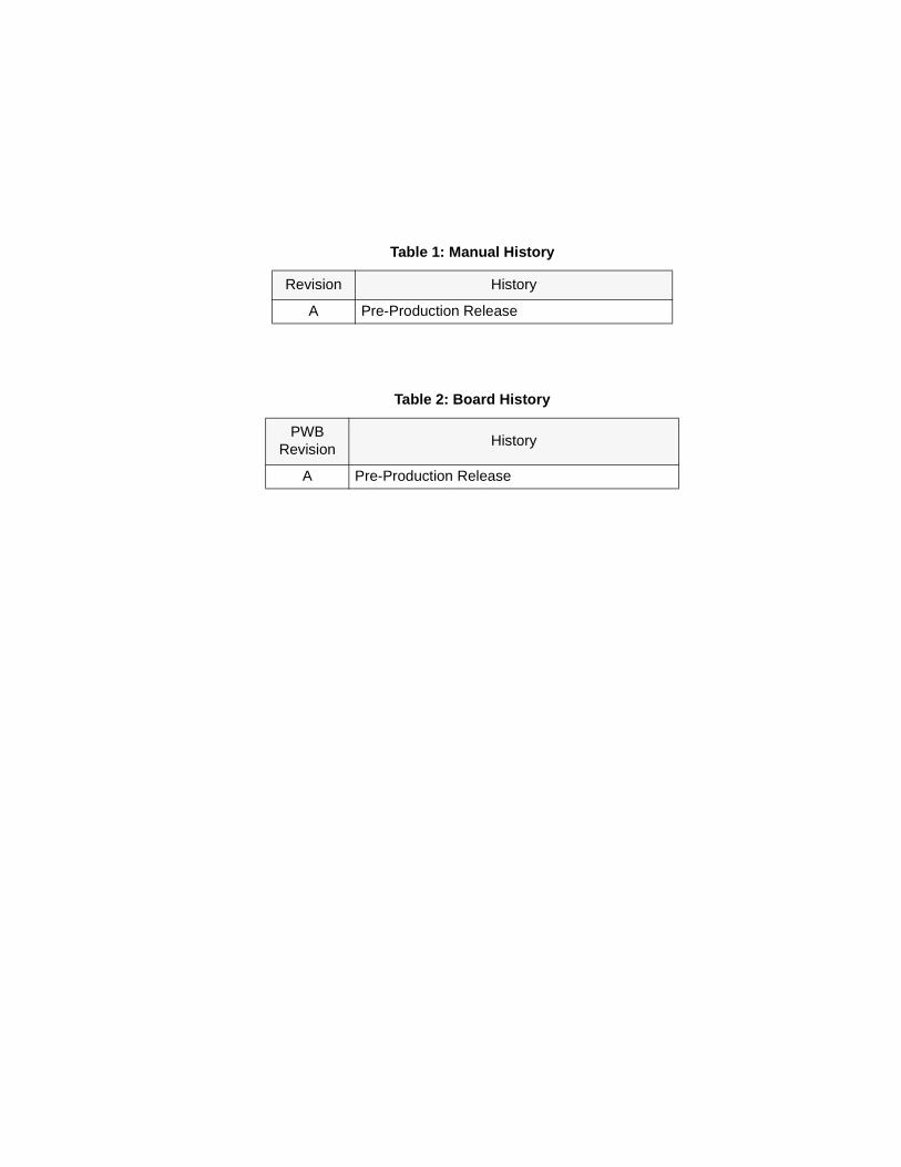
Table 1: Manual History
Revision History
A Pre-Production Release
Table 2: Board History
PWBRevision
History
A Pre-Production Release


1-1
Chapter 1
Introduction to the ADV7343 Daughter Card
Chapter One provides a description of the ADV7343 Daughter Card alongwith the key features of the circuit board.
Topic Page
1.1 Key Features 1-21.2 ADV7343 Daughter Card Installation 1-4
Spectrum Digital, Inc
1-2 ADV7343 Daughter Card Technical Reference
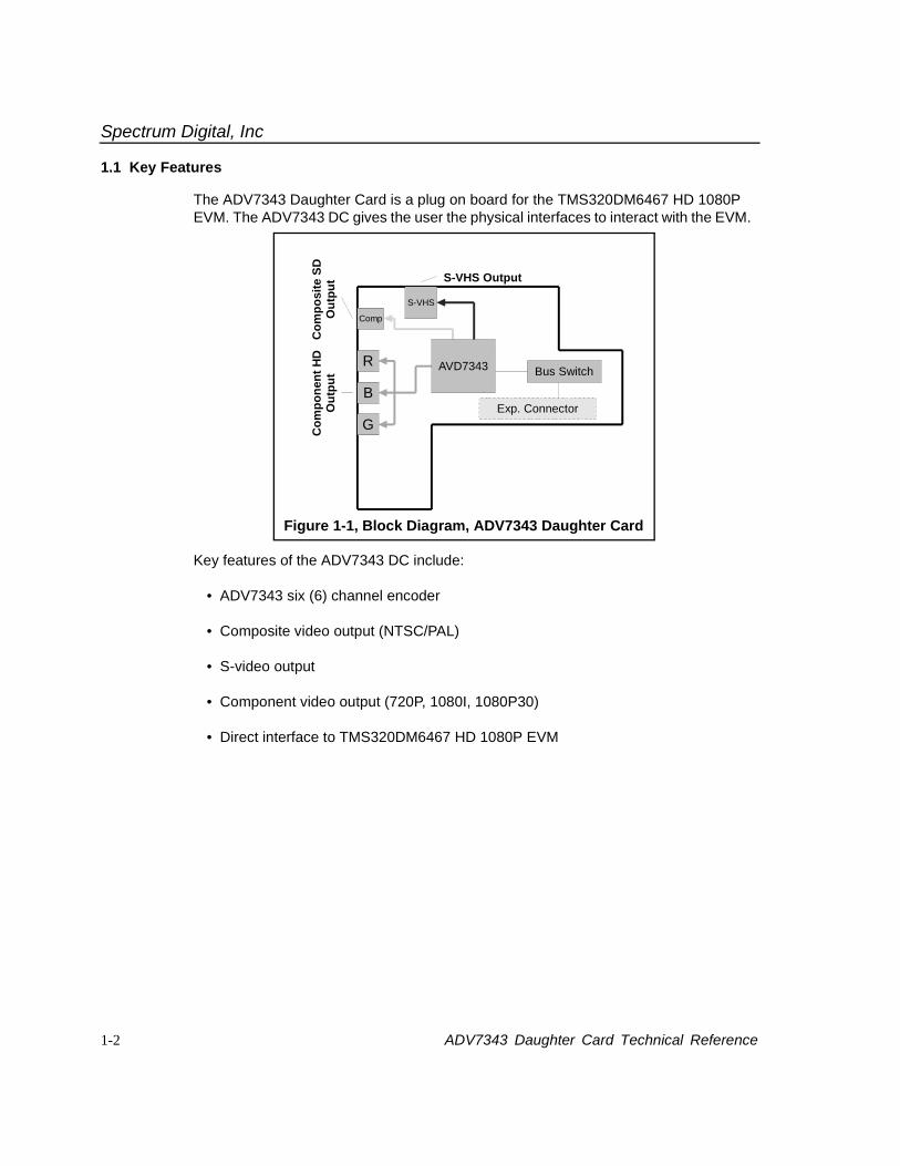
1.1 Key Features
The ADV7343 Daughter Card is a plug on board for the TMS320DM6467 HD 1080PEVM. The ADV7343 DC gives the user the physical interfaces to interact with the EVM.
Key features of the ADV7343 DC include:
• ADV7343 six (6) channel encoder
• Composite video output (NTSC/PAL)
• S-video output
• Component video output (720P, 1080I, 1080P30)
• Direct interface to TMS320DM6467 HD 1080P EVM
Figure 1-1, Block Diagram, ADV7343 Daughter Card
S-VHS
Bus Switch
Exp. Connector
S-VHS Output
Co
mp
osi
te S
DO
utp
ut
Co
mp
on
ent
HD
Ou
tpu
t
AVD7343
Comp
R
B
G
Spectrum Digital, Inc
1-3
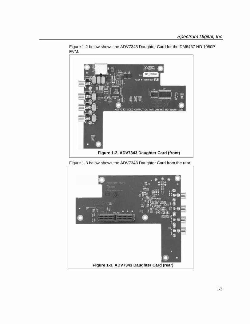
Figure 1-2 below shows the ADV7343 Daughter Card for the DM6467 HD 1080PEVM.
Figure 1-3 below shows the ADV7343 Daughter Card from the rear.
Figure 1-2, ADV7343 Daughter Card (front)
Figure 1-3, ADV7343 Daughter Card (rear)

Spectrum Digital, Inc
1-4 ADV7343 Daughter Card Technical Reference
1.2 ADV7343 Daughter Card Installation
The ADV7343 DC plugs directly onto the DM6467 HD 1080P EVM. To install this plug onboard follow the procedure below.
1. If the DM6467 EVM is in a chassis turn off the computer and remove the EVM.
2. If the DM6467 is being used standalone remove the power to the EVM by turning off the power (SW4) and removing the power plug (J15).
3. Attached two 5/8 inch standoffs to the bottom side of the ADV7343 board with 2 screws as shown in the figure below.
4. Align the DC_P2 connector on the bottom side of the ADV7343 with the DC_P2 connector on the top side of the EVM.
Figure 1-4, ADV7343 DC with Standoffs AttachedStandoff
Standoff
Screw
Screw
Figure 1-5, ADV7343 DC with Standoffs Attached
DC_P2 on EVM
DC_2 on ADV7343
Spectrum Digital, Inc
1-5
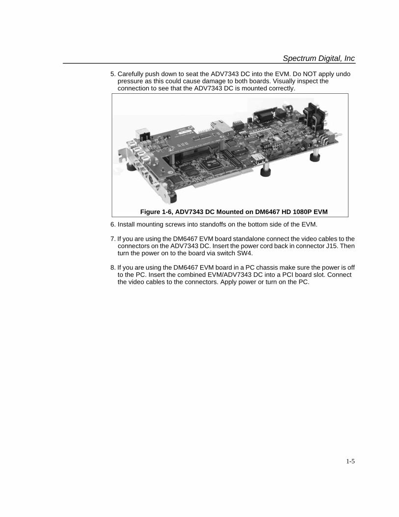
5. Carefully push down to seat the ADV7343 DC into the EVM. Do NOT apply undo pressure as this could cause damage to both boards. Visually inspect the connection to see that the ADV7343 DC is mounted correctly.
6. Install mounting screws into standoffs on the bottom side of the EVM.
7. If you are using the DM6467 EVM board standalone connect the video cables to the connectors on the ADV7343 DC. Insert the power cord back in connector J15. Then turn the power on to the board via switch SW4.
8. If you are using the DM6467 EVM board in a PC chassis make sure the power is off to the PC. Insert the combined EVM/ADV7343 DC into a PCI board slot. Connect the video cables to the connectors. Apply power or turn on the PC.
Figure 1-6, ADV7343 DC Mounted on DM6467 HD 1080P EVM

Spectrum Digital, Inc
1-6 ADV7343 Daughter Card Technical Reference

2-1
Chapter 2
Physical Description
This chapter describes the physical layout of the ADV7343 Daughter Cardand its interfaces.
Topic Page
2.1 Board Layout 2-22.2 Connectors 2-32.2.1 J1, Composite Video 2-32.2.2 J2, Pb Video Output 2-32.2.3 J3, Pr Video Output 2-42.2.4 J4, Y Video Output 2-42.2.5 P1, S-Video Connector 2-42.2.6 DC_P2, Video Expansion Connector 2-52.3 Test Points 2-72.4 Daughter Card Interface Control 2-8

Spectrum Digital, Inc
2-2 ADV7343 Daughter Card Technical Reference
2.1 Board Layout
The ADV7343 Daughter Card is a 4.70 x 5.75 inch (119 x 146 mm.) ten (10) layerprinted circuit board which is powered by an external +5 volt only power supply. Figure2-1 shows the layout of both sides of the ADV7343 Daughter Card.
J2
P1
J1
J3
J4
Figure 2-1, ADV7343 Daughter Card Interfaces
Top Side
Bottom side
DC_P2

Spectrum Digital, Inc
2-3
2.2 Connectors
The ADV7343 daughter Card has numerous connectors which provide connections tovarious peripherals. These connectors are described in the following sections.
2.2.1 J1, Composite Video
Connector J1 is a yellow RCA jack that brings out the composite video. This output isdriven by the CH1-OUT signal on the THS7314 via ADV7343 DAC_D. The figurebelow shows this RCA jack.
2.2.2 J2, Pb Video Output
Connector J2 is a blue RCA jack that brings out the Pb video component. This output isdriven by the CH2-OUT signal on the THS7303 via ADV7343 DAC_B. The figurebelow shows this RCA connector.
Table 1: Connectors
Connector Size SideSchematic
PageColor Function
J1 2 Top 5 Yellow Composite video
J2 2 Top 6 Blue Pb
J3 2 Top 6 Red Pr
J4 2 Top 6 Green Y
P1 6 Top 5 S-video
DC_P2 2 X 60 Bottom 2 Video Expansion
Figure 2-2, J1, RCA Jack
Shield (ground)
Signal Output
Figure 2-3, J2, RCA Jack
Shield (ground)
Signal Output

Spectrum Digital, Inc
2-4 ADV7343 Daughter Card Technical Reference
2.2.3 J3, Pr Video Output
Connector J3 is a red RCA jack that brings out the Pr video component. This output isdriven by the CH1-OUT signal on the THS7303 via ADV7343 DAC_C. The figurebelow shows this RCA connector.
2.2.4 J4, Y Video OUtput
Connector J4 is a green RCA jack that brings out the Y video component. This outputis driven by the CH3-OUT signal on the THS7303 via ADV7343 DAC_A. The figurebelow shows this RCA connector.
2.2.5 P1, S-Video Connector
Connector P1 is a 4 pin DIN connector that brings out the S-video. This output isdriven by the CH2-OUT and CH3-OUT signals on the THS7314 via the ADV7343DAC_E and DAC_F. The figure below shows the signals on this connector shows thisconnector as viewed from the card edge.
Figure 2-4, J3, RCA Jack
Shield (ground)
Signal Output
Figure 2-5, J4, RCA Jack
Shield (ground)
Signal Output
Ground - Pin 1 Pin 2 - GroundLUMA - Pin 3 Pin 4 - CHROMA
Figure 2-6, P1, Front View, Mini Din Connector

Spectrum Digital, Inc
2-5
2.2.6 DC_P2, Video Expansion Connector
The DC_P2 is a 120 pin SAMTEC high speed connector that interfaces to the videologic on the TMS320DM6467 EVM. The pinout for the pins 1-60 of theDC_P2 connector are shown in the table below.
Table 2: DC_P2, Video Expansion Connector, Pins 1-60
Pin # Signal Pin # Signal
1 ADV7343_ON_S0 2 VPIF_CLKOUT2
3 GROUND 4 GROUND
5 ADV7343_DC_PRESENT 6 ADV7343_ON_S1
7 GROUND 8 GROUND
9 VPIF_DOUT1 10 VPIF_DOUT0
11 VPIF_DOUT3 12 VPIF_DOUT2
13 VPIF_DOUT5 14 VPIF_DOUT4
15 VPIF_DOUT7 16 VPIF_DOUT6
17 GROUND 18 GROUND
19 VPIF_DOUT9 20 VPIF_DOUT8
21 VPIF_DOUT11 22 VPIF_DOUT10
23 VPIF_DOUT13 24 VPIF_DOUT12
25 VPIF_DOUT15 26 VPIF_DOUT14
27 GROUND 28 GROUND
29 VIDEO_OUT_EN1 30 VIDEO_OUT_EN0
31 GROUND 32 GROUND
33 NC 34 NC
35 GROUND 36 GROUND
37 NC 38 NC
39 GROUND 40 GROUND
41 NC 42 NC
43 GROUND 44 GROUND
45 NC 46 NC
47 NC 48 NC
49 GROUND 50 GROUND
51 NC 52 NC
53 NC 54 NC
55 NC 56 NC
57 NC 58 NC
59 ADV7343_ON_245 60 NC

Spectrum Digital, Inc
2-6 ADV7343 Daughter Card Technical Reference
The pinout for the pins 61-120 of the DC_P2 connector are shown in the table below.
Table 3: DC_P2, Video Expansion Connector, Pins 61-120
Pin # Signal Pin # Signal
61 GROUND 62 GROUND
63 NC 64 NC
65 NC 66 NC
67 GROUND 68 GROUND
69 NC 70 NC
71 NC 72 NC
73 NC 74 NC
75 GROUND 76 GROUND
77 I2C_SDA 78 I2C_SCL
79 NC 80 NC
81 GROUND 82 NC
83 NC 84 NC
85 GROUND 86 NC
87 NC 88 NC
89 GROUND 90 GROUND
91 NC 92 NC
93 GROUND 94 GROUND
95 NC 96 NC
97 NC 98 NC
99 NC 100 NC
101 NC 102 NC
103 GROUND 104 GROUND
105 NC 106 NC
107 NC 108 NC
109 NC 110 NC
111 NC 112 NC
113 GROUND 114 GROUND
115 VCC_3V3 116 VCC_3V3
117 GROUND 118 GROUND
119 VCC_5V 120 VCC_5V

Spectrum Digital, Inc
2-7
2.3 Test Points
The ADV7343 Daughter Card has 6 test points. All test points appear on the top of theboard. The following figure identifies the position of each test point. The next table listseach test point and the signal appearing on that test point.
Table 4: ADV7343 Daughter Card Test Points
TestPoint #
SchematicPage
Signal
TP1 6 GND
TP2 6 5V
TP3 6 3.3V
TP4 6 GND
TP5 6 GND
TP6 6 GND
Figure 2-7, ADV7343 Daughter Card, Test Points
TP2
TP6
TP1
TP5
TP3 TP4
Spectrum Digital, Inc
2-8 ADV7343 Daughter Card Technical Reference
2.4 Daughter Card Interface Control
When the ADV7343 Daughter Card is plugged into the DM6467 HD 1080P EVM theboard is detected to be an ADV7343 Daughter Card via control signals on theexpansion connector. The control signals interface to the CPLD on the DM6467 HD1080P EVM and automatically route the video output port of the DM6467 device to the
ADV7343 Daughter Card. Furthermore, the I2C interface to the THS8200 on the
DM6467 HD 1080P is disabled to prevent conflicts in the I2C addressing between videoencoders and video amplifiers on the two boards.

A-1
Appendix A
Schematics
This appendix contains the schematics for the ADV7343 Daughter Card.

Spectrum Digital, Inc
A-2 ADV7343 Daughter Card Technical Reference
5 5
4 4
3 3
2 2
1 1
DD
CC
BB
AA
Siz
e:
Da
te:
DW
G N
OR
evi
sio
n:
Sh
eet
of
Titl
e:
Pa
ge
Co
nte
nts
:
B
SP
EC
TR
UM
DIG
ITA
L I
NC
OR
PO
RA
TE
D
5120
82-0
001
Th
urs
day,
Oct
obe
r 2
9,
20
09
17
B
AD
V73
43
Da
ug
hte
r C
ard
fo
r D
M6
46
7 H
D 1
080
P E
VM
TIT
LE S
HE
ET
SHEET01 - TITLE
SHEET02 - VIDEO OUTPUT MUXING
SHEET03 - ADV7343
SHEET04 - COMPOSITE/S-VIDEO BUFFERING
SHEET05- COMPONENT VIDEO BUFFERING
SHEET06 - VIDEO DAUGHTER CARD CONN
SHEET07 - ADV7343 CORE POWER
SCHEMATIC CONTENTS
REV
ENGR
2REVISION STATUS OF SHEETS
1SH
DATE
DATE
ENGR-MGR
MFG
7
DWN
DATE
DATE
SH
DATE
CHK
RLSE
APPLICATION
REV
35
NEXT ASSY
DATE
6
DATE
QA
USED ON
4
BB
A
R.R.P.
T.W.K.
R.R.P.
R.R.P.
C.M.D.
R.R.P.
R.R.P.
01/15/2009
01/15/2009
01/15/2009
01/15/2009
01/15/2009
01/15/2009
01/15/2009
REV
SH
BB
AA
REV
REV
SH
SH
Initial schematic for layout
DESCRIPTION
REV
APPROVED
DATE
04/30/07
RRP
4. ALL 0.1 uF AND
0.01uF CAPACITORS
ARE DECOUPLING CAPS UNLESS
OTHERWISE NOTED.
THEY ARE SHOWN
ON THE PAGE WITH THE INTEGRATED
CIRCUITS THEY
SHOULD BE PLACED NEAR.
NOTES, UNLESS OTHERWISE SPECIFIED:
1. RESISTANCE VALUES IN OHMS.
2. CAPACTITANCE VALUES IN MICROFARADS.
3. LAST REFERENCE DESIGNATORS :
0x2A
ADV7343
I2C ADDRESS MAP
THS7303 - OUTPUT
0x2C
A
Changed ADV7343 output drive to reduce power
04/30/07
RRP
B
Spectrum Digital, Inc
A-3
5 5
4 4
3 3
2 2
1 1
DD
CC
BB
AA
VP
IF_
CLK
OU
T2
VP
IF_
DO
UT
1
VP
IF_
DO
UT
7
VP
IF_
DO
UT
3V
PIF
_D
OU
T5
VP
IF_
DO
UT
15V
PIF
_D
OU
T13
VP
IF_
DO
UT
11V
PIF
_D
OU
T9
VP
IF_
DO
UT
0V
PIF
_D
OU
T2
VP
IF_
DO
UT
6V
PIF
_D
OU
T4
VP
IF_
DO
UT
12
VP
IF_
DO
UT
10
VP
IF_
DO
UT
8
VP
IF_
DO
UT
14
VID
EO
_O
UT
_EN
0
I2C
_S
DA
I2C
_SC
L
AD
V7
34
3_
DC
_P
RE
SE
NT
VID
EO
_O
UT
_E
N1
VC
C_
5V
VC
C_
3V
3
VC
C_
5V
VC
C_
3V
3
VC
C_
3V
3
VC
C_
3V
3
VC
C_
3V
3
VC
C_
5V
VC
C_
3V
3
VP
IF_
CLK
OU
T2
3
VP
IF_
DO
UT
1_B
TM
13
VP
IF_
DO
UT
3_B
TM
33
VP
IF_
DO
UT
5_
PC
IEN
3V
PIF
_D
OU
T7
_SM
TR
FE
N3
VP
IF_
DO
UT
93
VP
IF_
DO
UT
113
VP
IF_
DO
UT
133
VP
IF_
DO
UT
153
VP
IF_D
OU
T0_
BT
M0
3V
PIF
_DO
UT
2_B
TM
23V
PIF
_DO
UT
4_
CS
2B
W3
VP
IF_
DO
UT
6_D
SP
BT
3
VP
IF_
DO
UT
83
VP
IF_D
OU
T1
03
VP
IF_D
OU
T1
23
VP
IF_D
OU
T1
43
I2C
_S
DA
4,6
I2C
_S
CL
4,6
AD
V7
343
_ON
_S0
3
AD
V73
43_
ON
_S
13
AD
V7
343
_ON
_245
3
Siz
e:
Da
te:
DW
G N
OR
evi
sio
n:
Sh
eet
of
Titl
e:
Pa
ge
Co
nte
nts
:
B
SP
EC
TR
UM
DIG
ITA
L IN
CO
RP
OR
AT
ED
5120
82-0
001
Th
urs
da
y, O
cto
be
r 2
9,
20
09
27
B
AD
V7
34
3 D
aug
hte
r C
ard
fo
r D
M6
467
HD
10
80P
EV
M
VID
EO
EX
PA
NS
ION
CO
NN
EC
TO
RS
TP
2
TE
ST
PO
INT
1
R1
947
0
TP
3
TE
ST
PO
INT
1TP
6
TE
ST
PO
INT
1
R1
847
0
R2
147
0
TP
5
TE
ST
PO
INT
1 TP
1
TE
ST
PO
INT
1
DC
_P
2C
ON
NE
CT
OR
60
X 2
11
22
33
44
55
66
77
88
99
1010
1111
1212
1313
1414
1515
1616
1717
1818
1919
2020
2121
2222
2323
2424
2525
2626
2727
2828
2929
3030
3131
3232
3333
3434
3535
3636
3737
3838
3939
4040
4141
4242
4343
4444
4545
4646
4747
4848
4949
5050
5151
5252
5353
5454
5555
5656
5757
5858
5959
6060
6161
6262
6363
6464
6565
6666
6767
6868
6969
7070
7171
7272
7373
7474
7575
7676
7777
7878
7979
8080
9090
8888
8686
8484
8282
8181
8383
8585
8787
8989
GND.1G1
GND.2G2
GND.3G3
GND.4G4
GND.5G5
GND.6G6
GND.7G7
GND.8G8
9191
9292
9393
9494
9595
9696
9797
9898
9999
100
100
101
101
102
102
103
103
104
104
105
105
106
106
107
107
108
108
109
109
110
110
111
111
112
112
113
113
114
114
115
115
116
116
117
117
118
118
119
119
120
120
TP
4
TE
ST
PO
INT
1

Spectrum Digital, Inc
A-4 ADV7343 Daughter Card Technical Reference
5 5
4 4
3 3
2 2
1 1
DD
CC
BB
AA
VID
4.1
V
VP
IF_
DO
UT
0V
PIF
_D
OU
T1
VP
IF_
DO
UT
2
VP
IF_
DO
UT
7V
PIF
_D
OU
T6
VP
IF_
DO
UT
3V
PIF
_D
OU
T4
_CS
2BW
VP
IF_
DO
UT
5
AD
V_
S2
AD
V_
S6
AD
V_
S7
AD
V_
S3
AD
V_
S5
AD
V_
S4
AD
V_
S1
AD
V_
S0
AD
V_
Y1
AD
V_
Y2
AD
V_
Y6
AD
V_
Y7
AD
V_
Y0
AD
V_
Y3
AD
V_
Y5
AD
V_
Y4
VP
IF_
DO
UT
15
VP
IF_
DO
UT
12
VP
IF_
DO
UT
13
VP
IF_
DO
UT
10
VP
IF_
DO
UT
8
VP
IF_
DO
UT
11
VP
IF_
DO
UT
9
VP
IF_
DO
UT
14
AD
V_
C1
AD
V_
C0
AD
V_
C2
AD
V_
C6
AD
V_
C7
AD
V_
C3
AD
V_
C5
AD
V_
C4
VID
_4
V1
VC
C_3
V3
VC
C_
5V
VC
C_
3V
3
AD
V73
43_O
N_2
452
AD
V73
43_O
N_S
02
AD
V73
43_O
N_S
12 V
PIF
_D
OU
T0
_BT
M0
2V
PIF
_D
OU
T1
_BT
M1
2V
PIF
_D
OU
T2
_BT
M2
2V
PIF
_D
OU
T3
_BT
M3
2VP
IF_
DO
UT
4_C
S2
BW
2V
PIF
_DO
UT
5_
PC
IEN
2V
PIF
_DO
UT
6_D
SP
BT
2VP
IF_D
OU
T7
_S
MT
RF
EN
2
AD
V_S
24
AD
V_S
34
AD
V_S
44
AD
V_S
54
AD
V_S
64
AD
V_S
74
AD
V_S
04
AD
V_S
14
AD
V_
Y2
4A
DV
_Y
34
AD
V_
Y4
4A
DV
_Y
54
AD
V_
Y6
4A
DV
_Y
74
AD
V_
Y0
4A
DV
_Y
14
VP
IF_D
OU
T8
2
VP
IF_D
OU
T9
2
VP
IF_
DO
UT
102
VP
IF_
DO
UT
112
VP
IF_
DO
UT
122
VP
IF_
DO
UT
132
VP
IF_
DO
UT
142
VP
IF_
DO
UT
152
AD
V_
C0
4
AD
V_
C1
4
AD
V_
C2
4
AD
V_
C3
4
AD
V_
C4
4
AD
V_
C5
4
AD
V_
C6
4
AD
V_
C7
4
VP
IF_
CL
KO
UT
22
AD
V_
VID
_C
LK
A4
Siz
e:
Da
te:
DW
G N
OR
evi
sio
n:
Sh
eet
of
Titl
e:
Pa
ge
Co
nte
nts
:
B
SP
EC
TR
UM
DIG
ITA
L I
NC
OR
PO
RA
TE
D
5120
82-0
001
Th
urs
day,
Oct
obe
r 2
9,
20
09
37
B
AD
V7
34
3 D
aug
hte
r C
ard
fo
r D
M6
467
HD
10
80P
EV
M
VID
EO
OU
TP
UT
MU
XE
S
S2
S1
S0
00
0
00
00 0
00
0
01
1 11
1 11
11
11
1
A Z Z ZB1
B2
B3
B2
B1
D3
LM
4040
DC
IM3-
4.1
21
U7
SN
74C
BT
162
14D
GG
R
S1
56
GND.2 19
1A2
11A
25
1B1
54
1B2
53
GND.1 8VCC.117
GND.3 38
GND.4 49
S2
55
2A4
3A6
4A9
5A11
6A13
7A15
8A18
9A21
10A
23
12A
27
1B3
3
2B3
5
3B3
7
4B3
10
5B3
12
6B3
14
7B3
16
8B3
20
S0
1
2B1
52
3B1
50
9B1
36
4B1
47
5B1
45
6B1
43
7B1
41
8B1
39
10B
134
2B2
51
3B2
48
4B2
46
5B2
44
6B2
42
7B2
40
8B2
37
11B
231
12B
229
9B3
22
10B
324
11B
326
12B
328
11B
132
12B
130
9B2
35
10B
233
C2
8
56
0pF
R4
20
C2
90
.1u
F
U8
SN
74C
BT
LV1
G12
5
3
4
5
2
1
R2
036
0
C5
6.1
uF
U6
SN
74C
BT
LV33
84P
W
1A1
3
1A2
4
1A3
7
1A4
8
1A5
11
2A1
14
2A2
17
2A3
18
2A4
21
2A5
22
1B1
2
1B2
5
1B3
6
1B4
9
1B5
10
2B1
15
2B2
16
2B3
19
2B4
20
2B5
23
VC
C24
GN
D12
1OE
1
2OE
13
R1
1.5
K
C2
20
.1u
F

Spectrum Digital, Inc
A-5
5 5
4 4
3 3
2 2
1 1
DD
CC
BB
AA
AD
V_
S7
AD
V_
S0
AD
V_
S4
AD
V_
S5
AD
V_
S6
AD
V_
S1
AD
V_
S3
AD
V_
S2
AD
V_
Y7
AD
V_
Y0
AD
V_
Y4
AD
V_
Y5
AD
V_
Y6
AD
V_
Y1
AD
V_
Y3
AD
V_
Y2
AD
V_C
7
AD
V_C
0
AD
V_C
4A
DV
_C5
AD
V_C
6
AD
V_C
1
AD
V_C
3
AD
V_C
2
VR
EF
_1
.24
V
GN
D_E
NC
AD
V_
VC
C_3
V3
GN
D_E
NC
GN
D_E
NC
GN
D_E
NC
VC
C_
3V
3
VC
C_3
V3
GN
D_E
NC
GN
D_E
NC
GN
D_E
NC
AD
V_1
.8V
VC
C_
3V
3A
DV
_V
CC
_3V
3
PV
DD
PV
DD P
VD
D
PV
DD
AD
V_
1.8
V
VC
C_
3V3
GN
D_E
NC
AD
V_
VID
_C
LK
A3
AD
V_
S0
3A
DV
_S
13
AD
V_
S2
3A
DV
_S
33
AD
V_
S4
3A
DV
_S
53
AD
V_
S6
3A
DV
_S
73
AD
V_
Y0
3A
DV
_Y
13
AD
V_
Y2
3A
DV
_Y
33
AD
V_
Y4
3A
DV
_Y
53
AD
V_
Y6
3A
DV
_Y
73
AD
V_
C0
3
AD
V_
C1
3A
DV
_C
23
AD
V_
C3
3A
DV
_C
43
AD
V_
C5
3A
DV
_C
63
AD
V_
C7
3
I2C
_S
DA
2,6
I2C
_S
CL
2,6
AD
V_
DA
C_
16
AD
V_
DA
C_
55
AD
V_
DA
C_
65
AD
V_
DA
C_
45
AD
V_
DA
C_
26
AD
V_
DA
C_
36
Siz
e:
Da
te:
DW
G N
OR
evi
sio
n:
Sh
eet
of
Titl
e:
Pa
ge
Co
nte
nts
:
B
SP
EC
TR
UM
DIG
ITA
L IN
CO
RP
OR
AT
ED
5120
82-0
001
Th
urs
da
y, O
cto
be
r 2
9,
20
09
47
B
AD
V7
34
3 D
aug
hte
r C
ard
fo
r D
M6
467
HD
10
80P
EV
M
AD
V7
34
3 V
IDE
O E
NC
OD
ER
FOOTPRINT FOR TLV431ADBV
+C
12
10
uF
R2
41
020
1%
L8
BL
M2
1PG
221
SN
1D
R2
64
.12
K 1
%
C1
6
0.0
1uF
R8
NO
-PO
P
R1
01
69 1
%
R4
10
C4
1
0.0
1u
F
C4
0
0.1
uF
C3
4
0.1
uF
R6
NO
-PO
P
R2
2N
O-P
OP
L4
BLM
21P
G22
1SN
1D
C3
5.1
50
uF
R2
9N
O-P
OP
R2
3N
O-P
OP
+C
11
10
uF
C4
3.1
uF
R2
51
69 1
%
R1
1N
O-P
OP
C3
2
0.1
uF
R2
7N
O-P
OP
C3
6.0
12
uF
C3
9
0.1
uF
R2
8N
O-P
OP
R4
0
L7
BLM
21P
G2
21S
N1D
L3
BL
M2
1PG
221
SN
1D
L5
BL
M2
1PG
221
SN
1D
L6
BLM
21P
G2
21S
N1D C
23
.15
0u
F
C4
2.1
uF
C38
22
00p
F
C45
1u
F
+C
10
10u
F
C4
4
0.0
1u
F
R9
NO
-PO
P
C3
1
0.0
1u
F
C37
22
00p
F
C2
4.0
12
uF
+C
15
10u
F
U5
AD
V73
43
VD
DIO
.11
TE
ST
02
TE
ST
13
Y0
4
Y1
5
Y2
6
Y3
7
Y4
8
Y5
9
VD
D.1
10
DG
ND
.111
Y6
12
Y7
13
TE
ST
214
TE
ST
315
C0
16C1 17
C2 18
ALSB/SPI_I2S 19
SDA/SCLK 20
SCL/MOSI 21
P_HYSNCn 22
P_VSYNCn 23
P_BLANKn 24
C3 25
C4 26
C5 27
C6 28
C7 29
CLKIN_A 30
EXT_LF2 31
PGND 32
EX
T_L
F1
33P
VD
D.1
34
RS
ET
236
CO
MP
235
DA
C_F
37D
AC
_E38
DA
C_D
39A
GN
D.1
40V
AA
.141
DA
C_C
42D
AC
_B43
DA
C_A
44C
OM
P1
45V
RE
F46
RS
ET
147
S_F
L/M
ISO
48
S_VSYNCn49S_HYSNCn50
TEST451TEST552
S053S154S255
VDD.256DGND.257
S358S459S560S661S762
CLKIN_B63GND.IO164
C3
3
0.1
uF
U4
NO
-PO
P
53
4

Spectrum Digital, Inc
A-6 ADV7343 Daughter Card Technical Reference
5 5
4 4
3 3
2 2
1 1
DD
CC
BB
AA
S-V
IDE
O_L
UM
A
GN
D_E
NC
AD
V_
VC
C_3
V3
GN
D_E
NC
GN
D_E
NC
GN
D_E
NC
GN
D_E
NC
GN
D_E
NC
GN
D_E
NC
GN
D_E
NC
GN
D_E
NC
GN
D_E
NC
AD
V_
DA
C_
44
AD
V_
DA
C_
54
AD
V_
DA
C_
64
Siz
e:
Da
te:
DW
G N
OR
evi
sio
n:
Sh
eet
of
Titl
e:
Pa
ge
Co
nte
nts
:
A
SP
EC
TR
UM
DIG
ITA
L I
NC
OR
PO
RA
TE
D
5120
82-0
001
Th
urs
day,
Oct
obe
r 2
9,
20
09
57
B
AD
V7
34
3 D
aug
hte
r C
ard
fo
r D
M6
467
HD
10
80P
EV
M
CO
MP
OS
ITE
/S-V
IDE
O O
UT
PU
T
COMPOSITE
DAC_4 COMPOSITE VIDEO
DAC_5 LUMA
DAC_6 CHROMA
R1
67
5 1
%
C2
1
.01
uF
C2
60
.1u
F
R1
57
5 1%
C2
70
.1u
F
+
C1
33
0uF
C2
5
.1u
F
C8
33
uF
R1
77
5 1
%
J1R
CA
JA
CK
2
14
3
+
C2
33
0uF
R12
30
1 1
%
P1
7491
81-1
34 2
1
56
L2B
EA
D
R1
33
01
1%
+
C7
33
0uF
R1
430
1 1
%
C9
33
uF
C3
00
.1u
F
U1
TH
S73
14
CH
1-O
UT
8
GN
D5
CH
1-IN
1
VS
+4
CH
2-O
UT
7
CH
3-O
UT
6
CH
2-IN
2
CH
3-IN
3

Spectrum Digital, Inc
A-7
5 5
4 4
3 3
2 2
1 1
DD
CC
BB
AA
I2C
_SD
A_
7303
I2C
_S
DA
I2C
_SC
LI2
C_
SC
L_7
303
GN
D_E
NC
GN
D_E
NC
GN
D_E
NC
GN
D_E
NC
GN
D_E
NC
GN
D_E
NC
GN
D_E
NC
GN
D_E
NC
GN
D_E
NC
GN
D_E
NC
GN
D_E
NC
GN
D_E
NC
GN
D_E
NC
GN
D_E
NC
VC
C_
3V
3
GN
D_E
NC
GN
D_E
NC
I2C
_S
DA
2,4
I2C
_S
CL
2,4
AD
V_
DA
C_
34
AD
V_
DA
C_
14
AD
V_
DA
C_
24
Siz
e:
Da
te:
DW
G N
OR
evi
sio
n:
Sh
eet
of
Titl
e:
Pa
ge
Co
nte
nts
:
B
SP
EC
TR
UM
DIG
ITA
L I
NC
OR
PO
RA
TE
D
5120
82-0
001
Th
urs
day,
Oct
obe
r 2
9,
20
09
67
B
AD
V7
34
3 D
aug
hte
r C
ard
fo
r D
M6
467
HD
10
80P
EV
M
VID
EO
OU
TP
UT
DAC_1 G/Y
DAC_2 B/PB
DAC_3 R/PR
ORDER IS RED,BLUE,GREEN ON BULKHEAD
NOTE:
R3
30
C46
1u
FC
48
.01u
F
R4
07
5
R3
00
J4R
CA
JA
CK
2
14
3
R3
77
5 1%
R3
57
5 1
%R
32
75
1%
J3R
CA
JA
CK
2
14
3
C4
9N
O-P
OP
R3
60
C5
1N
O-P
OP
L1B
EA
D
C4
7N
O-P
OP
+
C1
43
30u
F
R3
410
0
C5
33u
F
C6
33
uF
C5
2
22
pF
C5
5.0
1uF
J2R
CA
JA
CK
2
14
3
R3
975
C5
0
22
pF
+
C1
33
30u
F
R3
110
0
C5
4.0
1uF
C5
3.0
1uF
R3
875
+
C4
33
0uF
U3
TH
S73
03
NC
11
NC
2020
I2C
-A1
8
I2C
-SD
A12
I2C
-SC
L13
CH
1-O
UT
19
CH
1-S
AG
18
VS
+11
CH
1-IN
A2
GN
D.1
10
I2C
-A0
9
CH
2-O
UT
17
CH
2-S
AG
16
CH
3-O
UT
15
CH
3-S
AG
14
CH
2-IN
A3
CH
3-IN
A4
CH
1-IN
B5
CH
2-IN
B6
CH
3-IN
B7

Spectrum Digital, Inc
A-8 ADV7343 Daughter Card Technical Reference
5 5
4 4
3 3
2 2
1 1
DD
CC
BB
AA
AD
V_
1.8V
VC
C_
5V
VC
C_3
V3
Siz
e:
Da
te:
DW
G N
OR
evi
sio
n:
Sh
eet
of
Titl
e:
Pa
ge
Co
nte
nts
:
A
SP
EC
TR
UM
DIG
ITA
L I
NC
OR
PO
RA
TE
D
5120
82-0
001
Tue
sda
y, O
ctob
er
27,
20
09
77
B
AD
V7
34
3 D
aug
hte
r C
ard
fo
r D
M6
467
HD
10
80P
EV
M
AD
V7
343
CO
RE
PO
WE
R
PLACE NEAR ADV7343
R2
6.1
9K
R7
4.9
9K
R5
1K
R3
10K
U2
TP
S74
701
IN1
1V
OU
T2
10
BIA
S4
PG
3
EN
5G
ND
6
IN2
2
SS
7F
B8
VO
UT
19
PP1 11
PP2 12
PP3 13
PP4 14
C3
10u
F
C1
7
10
uF
D1
MU
RS
120
T3
C1
91
uF
C20
0.0
01u
F
D2
MU
RS
120T
3
C1
85
.6p
F
B-1
Appendix B
Mechanical Information
This appendix contains the mechanical information about the ADV7343Daughter Card produced by Spectrum Digital.

Spectrum Digital, Inc
B-2 ADV7343 Daughter Card Technical Reference
TH
IS D
RA
WIN
G IS
NO
T T
O S
CA
LEA
LL D
IME
NS
ION
S A
RE
IN IN
CH
ES
Top
Vie
w

Spectrum Digital, Inc
B-3
TH
IS D
RA
WIN
G IS
NO
T T
O S
CA
LEA
LL D
IME
NS
ION
S A
RE
IN IN
CH
ES
Bot
tom
Vie
w

Spectrum Digital, Inc
B-4 ADV7343 Daughter Card Technical Reference


Printed in U.S.A., November 2009512085-0001 Rev A