adum6000 (rev. d)
TRANSCRIPT

Isolated, 5 kV, DC-to-DC ConverterData Sheet ADuM6000
Rev. D Document Feedback Information furnished by Analog Devices is believed to be accurate and reliable. However, no responsibility is assumed by Analog Devices for its use, nor for any infringements of patents or other rights of third parties that may result from its use. Specifications subject to change without notice. No license is granted by implication or otherwise under any patent or patent rights of Analog Devices. Trademarks and registered trademarks are the property of their respective owners.
One Technology Way, P.O. Box 9106, Norwood, MA 02062-9106, U.S.A.Tel: 781.329.4700 ©2010–2013 Analog Devices, Inc. All rights reserved. Technical Support www.analog.com
FEATURES isoPower integrated, isolated dc-to-dc converter Regulated 5 V or 3.3 V output Up to 400 mW output power 16-lead SOIC wide-body package (RW-16) 16-lead SOIC wide-body package with enhanced
creepage (RI-16-2) High temperature operation: 105°C maximum High common-mode transient immunity: >25 kV/μs Thermal overload protection Safety and regulatory approvals
UL recognition 5000 V rms for 1 minute per UL 1577
CSA Component Acceptance Notice #5A (pending) IEC 60601-1: 250 V rms, 8 mm package (RI-16-2) IEC 60950-1: 400 V rms, 8 mm package (RI-16-2)
VDE certificate of conformity (RW-16) (pending) IEC 60747-5-2 (VDE 0884 Part 2):2003-01 VIORM = 846 V peak
VDE certificate of conformity (RI-16-2) DIN V VDE V 0884-10 (VDE V 0884-10):2006-12 VIORM = 846 V peak
APPLICATIONS USB peripheral power RS-232/RS-422/RS-485 transceiver power Industrial field bus power Industrial PLCs
GENERAL DESCRIPTION The ADuM60001 is an isolated dc-to-dc converter based on the Analog Devices, Inc., iCoupler® technology. The dc-to-dc converter in this device provides regulated, isolated power in several combi-nations of input and output voltages as listed in Table 1.
The Analog Devices chip scale transformer iCoupler technology transfers isolated power in this dc-to-dc converter with up to 31% efficiency. The result is a small form factor, total isolation solution.
Higher output power levels are obtained by using the ADuM6000 to augment the power output of the ADuM5401, ADuM5402, ADuM5403, ADuM5404, ADuM520x, and ADuM620x iCouplers with isoPower®.
isoPower uses high frequency switching elements to transfer power through its transformer. Special care must be taken during printed circuit board (PCB) layout to meet emissions standards. See the AN-0971 Application Note for board layout recommendations.
Table 1. Power Levels Input Voltage Output Voltage Output Power 5 V 5 V 400 mW 5 V 3.3 V 330 mW 3.3 V 3.3 V 132 mW
FUNCTIONAL BLOCK DIAGRAM
VDD1
GND1
NC
RCIN
RCOUT
RCSEL
VDD1
OSCILLATOR
GND1
VISO
GNDISO
NC
VSEL
NC
NC
VISO
GNDISO
1
2
3
4
5
6
7
8
16
15
14
13
12
11
10
9ADuM6000
RECTIFIER REGULATOR
0862
4-00
1
Figure 1.
1 Protected by U.S. Patents 5,952,849; 6,873,065; 6,903,578; and 7,075,329; other patents pending.
ADuM6000 Data Sheet
Rev. D | Page 2 of 16
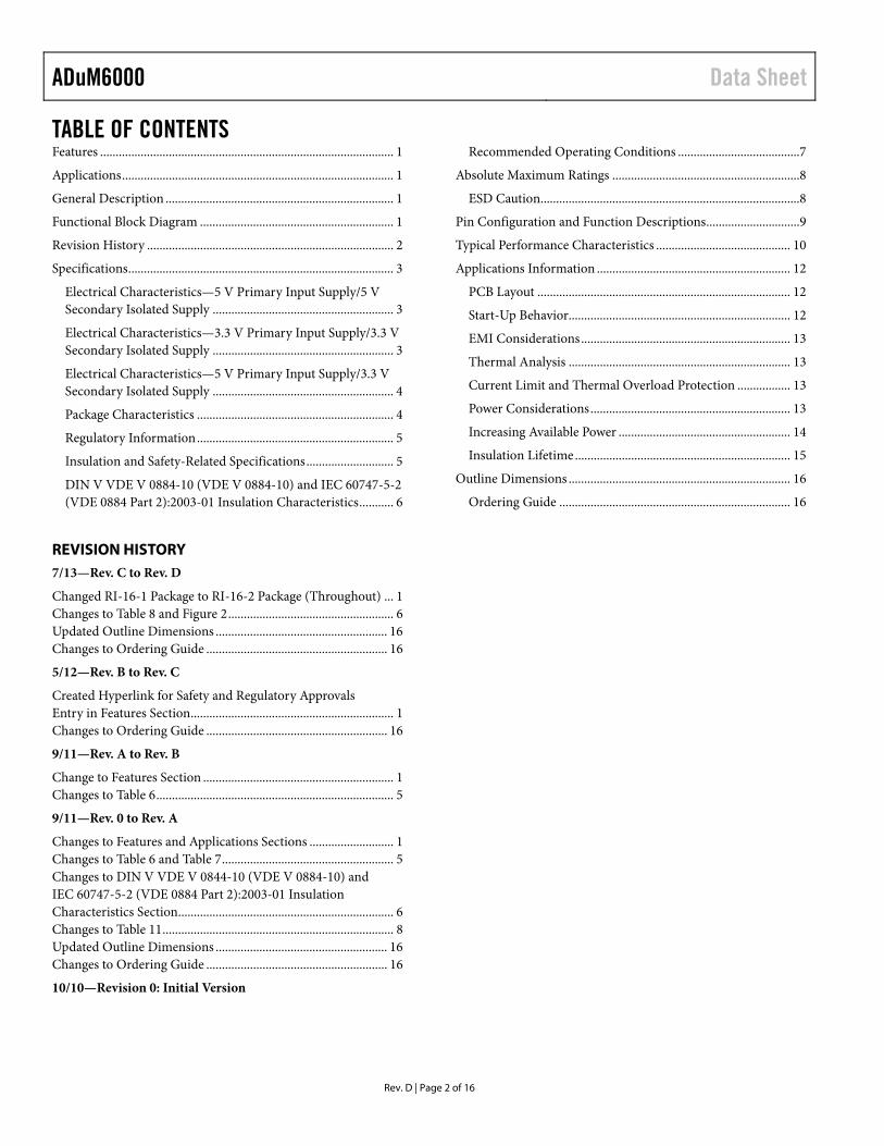
TABLE OF CONTENTS Features .............................................................................................. 1 Applications ....................................................................................... 1 General Description ......................................................................... 1 Functional Block Diagram .............................................................. 1 Revision History ............................................................................... 2 Specifications ..................................................................................... 3
Electrical Characteristics—5 V Primary Input Supply/5 V Secondary Isolated Supply .......................................................... 3 Electrical Characteristics—3.3 V Primary Input Supply/3.3 V Secondary Isolated Supply .......................................................... 3 Electrical Characteristics—5 V Primary Input Supply/3.3 V Secondary Isolated Supply .......................................................... 4 Package Characteristics ............................................................... 4 Regulatory Information ............................................................... 5 Insulation and Safety-Related Specifications ............................ 5 DIN V VDE V 0884-10 (VDE V 0884-10) and IEC 60747-5-2 (VDE 0884 Part 2):2003-01 Insulation Characteristics ........... 6
Recommended Operating Conditions .......................................7 Absolute Maximum Ratings ............................................................8
ESD Caution...................................................................................8 Pin Configuration and Function Descriptions ..............................9 Typical Performance Characteristics ........................................... 10 Applications Information .............................................................. 12
PCB Layout ................................................................................. 12 Start-Up Behavior....................................................................... 12 EMI Considerations ................................................................... 13 Thermal Analysis ....................................................................... 13 Current Limit and Thermal Overload Protection ................. 13 Power Considerations ................................................................ 13 Increasing Available Power ....................................................... 14 Insulation Lifetime ..................................................................... 15
Outline Dimensions ....................................................................... 16 Ordering Guide .......................................................................... 16
REVISION HISTORY 7/13—Rev. C to Rev. D
Changed RI-16-1 Package to RI-16-2 Package (Throughout) ... 1 Changes to Table 8 and Figure 2 ..................................................... 6 Updated Outline Dimensions ....................................................... 16 Changes to Ordering Guide .......................................................... 16
5/12—Rev. B to Rev. C
Created Hyperlink for Safety and Regulatory Approvals Entry in Features Section ................................................................. 1 Changes to Ordering Guide .......................................................... 16
9/11—Rev. A to Rev. B
Change to Features Section ............................................................. 1 Changes to Table 6 ............................................................................ 5
9/11—Rev. 0 to Rev. A
Changes to Features and Applications Sections ........................... 1 Changes to Table 6 and Table 7 ....................................................... 5 Changes to DIN V VDE V 0844-10 (VDE V 0884-10) and IEC 60747-5-2 (VDE 0884 Part 2):2003-01 Insulation Characteristics Section ..................................................................... 6 Changes to Table 11 .......................................................................... 8 Updated Outline Dimensions ....................................................... 16 Changes to Ordering Guide .......................................................... 16
10/10—Revision 0: Initial Version

Data Sheet ADuM6000
Rev. D | Page 3 of 16
SPECIFICATIONS ELECTRICAL CHARACTERISTICS—5 V PRIMARY INPUT SUPPLY/5 V SECONDARY ISOLATED SUPPLY 4.5 V ≤ VDD1 ≤ 5.5 V, VSEL = VISO; each voltage is relative to its respective ground. Minimum/maximum specifications apply over the entire recommended operating range, unless otherwise noted. Typical specifications are at TA = 25°C, VDD1 = 5.0 V, VISO = 5.0 V, and VSEL = VISO.
Table 2. Parameter Symbol Min Typ Max Unit Test Conditions/Comments DC-TO-DC CONVERTER POWER SUPPLY
Setpoint VISO 4.7 5.0 5.4 V IISO = 0 mA Line Regulation VISO(LINE) 1 mV/V IISO = 40 mA, VDD1 = 4.5 V to 5.5 V Load Regulation VISO(LOAD) 1 5 % IISO = 8 mA to 72 mA Output Ripple VISO(RIP) 75 mV p-p 20 MHz bandwidth, CBO = 0.1 μF||10 μF,
IISO = 72 mA Output Noise VISO(N) 200 mV p-p CBO = 0.1 μF||10 μF, IISO = 72 mA Switching Frequency fOSC 180 MHz PWM Frequency fPWM 625 kHz IDD1 Supply Current, Full VISO Load IDD1(MAX) 290 mA
Maximum Output Supply Current IISO(MAX) 80 mA VISO > 4.5 V Efficiency at Maximum Output
Supply Current 31 % IISO = 80 mA
IDD1 Supply Current, No VISO Load IDD1(Q) 7 16 mA IISO = 0 mA Undervoltage Lockout, VDD1 and VISO
Supplies UVLO
Positive-Going Threshold VUV+ 2.7 V Negative-Going Threshold VUV− 2.4 V Hysteresis VUVH 0.3 V
ELECTRICAL CHARACTERISTICS—3.3 V PRIMARY INPUT SUPPLY/3.3 V SECONDARY ISOLATED SUPPLY 3.0 V ≤ VDD1 ≤ 3.6 V, VSEL = GNDISO; each voltage is relative to its respective ground. Minimum/maximum specifications apply over the entire recommended operating range, unless otherwise noted. Typical specifications are at TA = 25°C, VDD1 = 3.3 V, VISO = 3.3 V, and VSEL = GNDISO.
Table 3. Parameter Symbol Min Typ Max Unit Test Conditions/Comments DC-TO-DC CONVERTER POWER SUPPLY
Setpoint VISO 3.0 3.3 3.6 V IISO = 0 mA Line Regulation VISO(LINE) 1 mV/V IISO = 20 mA, VDD1 = 3.0 V to 3.6 V Load Regulation VISO(LOAD) 1 5 % IISO = 4 mA to 36 mA Output Ripple VISO(RIP) 50 mV p-p 20 MHz bandwidth, CBO = 0.1 μF||10 μF,
IISO = 36 mA Output Noise VISO(N) 130 mV p-p CBO = 0.1 μF||10 μF, IISO = 36 mA Switching Frequency fOSC 180 MHz PWM Frequency fPWM 625 kHz IDD1 Supply Current, Full VISO Load IDD1(MAX) 175 mA
Maximum Output Supply Current IISO(MAX) 40 mA VISO > 3.0 V Efficiency at Maximum Output
Supply Current 31 % IISO = 40 mA
IDD1 Supply Current, No VISO Load IDD1(Q) 5 13 mA IISO = 0 mA Undervoltage Lockout, VDD1 and VISO
Supplies UVLO
Positive-Going Threshold VUV+ 2.7 V Negative-Going Threshold VUV− 2.4 V Hysteresis VUVH 0.3 V
ADuM6000 Data Sheet
Rev. D | Page 4 of 16
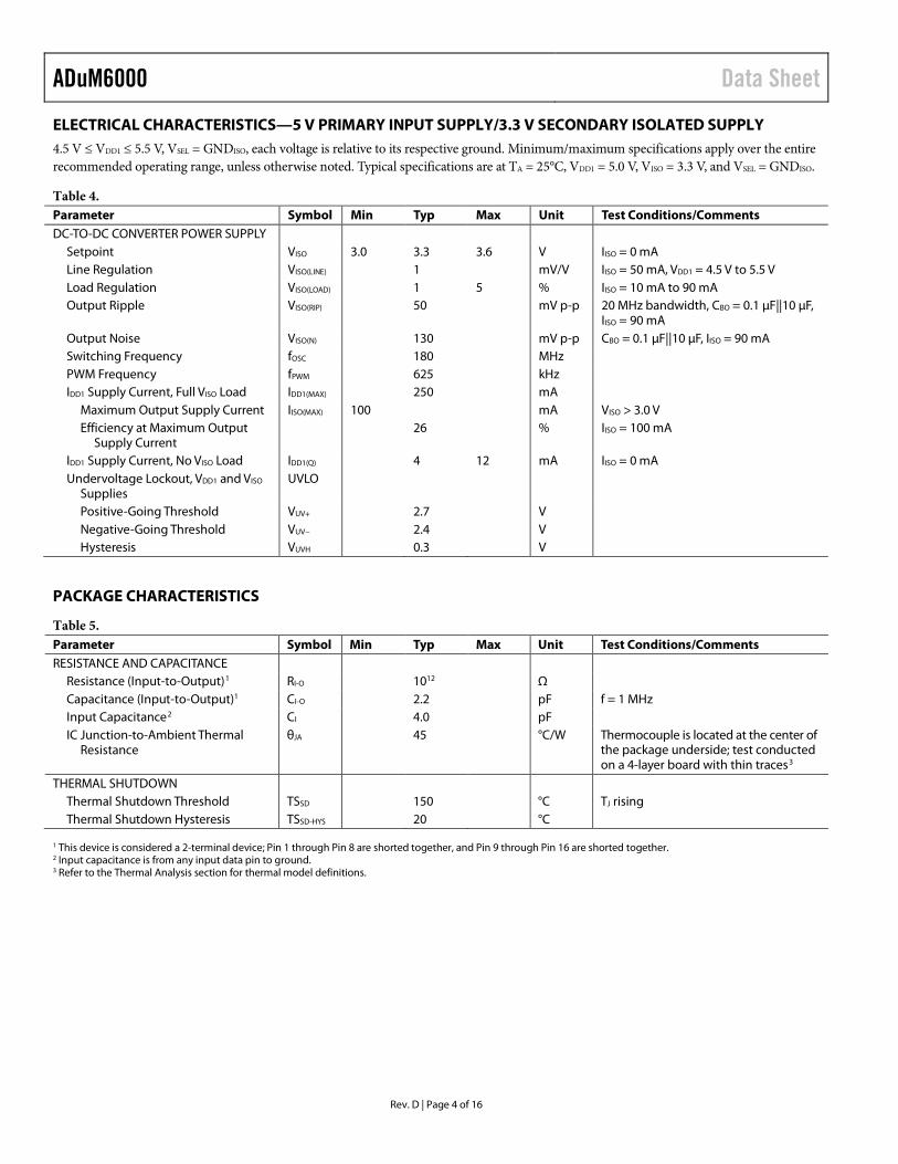
ELECTRICAL CHARACTERISTICS—5 V PRIMARY INPUT SUPPLY/3.3 V SECONDARY ISOLATED SUPPLY 4.5 V ≤ VDD1 ≤ 5.5 V, VSEL = GNDISO, each voltage is relative to its respective ground. Minimum/maximum specifications apply over the entire recommended operating range, unless otherwise noted. Typical specifications are at TA = 25°C, VDD1 = 5.0 V, VISO = 3.3 V, and VSEL = GNDISO.
Table 4. Parameter Symbol Min Typ Max Unit Test Conditions/Comments DC-TO-DC CONVERTER POWER SUPPLY
Setpoint VISO 3.0 3.3 3.6 V IISO = 0 mA Line Regulation VISO(LINE) 1 mV/V IISO = 50 mA, VDD1 = 4.5 V to 5.5 V Load Regulation VISO(LOAD) 1 5 % IISO = 10 mA to 90 mA Output Ripple VISO(RIP) 50 mV p-p 20 MHz bandwidth, CBO = 0.1 μF||10 μF,
IISO = 90 mA Output Noise VISO(N) 130 mV p-p CBO = 0.1 μF||10 μF, IISO = 90 mA Switching Frequency fOSC 180 MHz PWM Frequency fPWM 625 kHz IDD1 Supply Current, Full VISO Load IDD1(MAX) 250 mA
Maximum Output Supply Current IISO(MAX) 100 mA VISO > 3.0 V Efficiency at Maximum Output
Supply Current 26 % IISO = 100 mA
IDD1 Supply Current, No VISO Load IDD1(Q) 4 12 mA IISO = 0 mA Undervoltage Lockout, VDD1 and VISO
Supplies UVLO
Positive-Going Threshold VUV+ 2.7 V Negative-Going Threshold VUV− 2.4 V Hysteresis VUVH 0.3 V
PACKAGE CHARACTERISTICS
Table 5. Parameter Symbol Min Typ Max Unit Test Conditions/Comments RESISTANCE AND CAPACITANCE
Resistance (Input-to-Output)1 RI-O 1012 Ω Capacitance (Input-to-Output)1 CI-O 2.2 pF f = 1 MHz Input Capacitance2 CI 4.0 pF IC Junction-to-Ambient Thermal
Resistance θJA 45 °C/W Thermocouple is located at the center of
the package underside; test conducted on a 4-layer board with thin traces3
THERMAL SHUTDOWN Thermal Shutdown Threshold TSSD 150 °C TJ rising Thermal Shutdown Hysteresis TSSD-HYS 20 °C
1 This device is considered a 2-terminal device; Pin 1 through Pin 8 are shorted together, and Pin 9 through Pin 16 are shorted together. 2 Input capacitance is from any input data pin to ground. 3 Refer to the Thermal Analysis section for thermal model definitions.
Data Sheet ADuM6000
Rev. D | Page 5 of 16
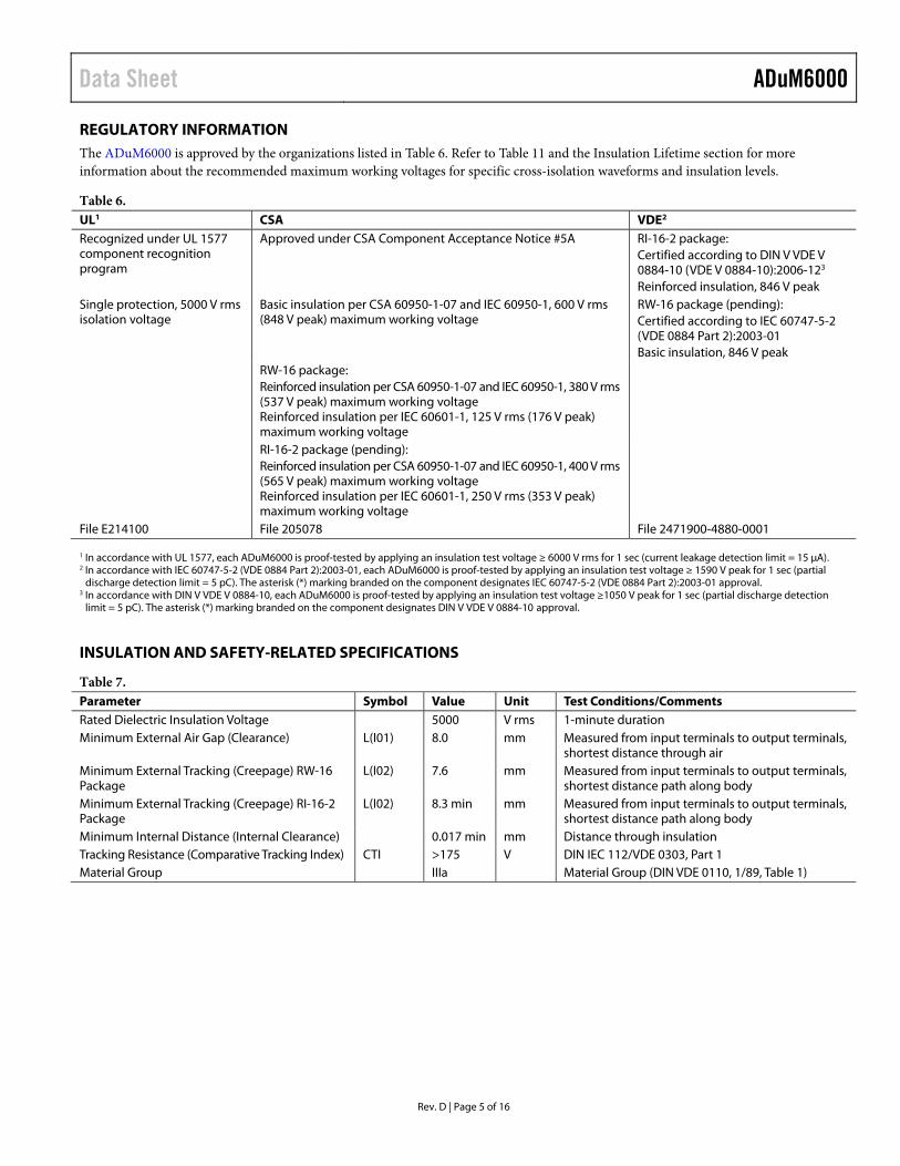
REGULATORY INFORMATION The ADuM6000 is approved by the organizations listed in Table 6. Refer to Table 11 and the Insulation Lifetime section for more information about the recommended maximum working voltages for specific cross-isolation waveforms and insulation levels.
Table 6. UL1 CSA VDE2 Recognized under UL 1577 component recognition program
Approved under CSA Component Acceptance Notice #5A RI-16-2 package: Certified according to DIN V VDE V 0884-10 (VDE V 0884-10):2006-123 Reinforced insulation, 846 V peak
Single protection, 5000 V rms isolation voltage
Basic insulation per CSA 60950-1-07 and IEC 60950-1, 600 V rms (848 V peak) maximum working voltage
RW-16 package (pending): Certified according to IEC 60747-5-2 (VDE 0884 Part 2):2003-01 Basic insulation, 846 V peak
RW-16 package: Reinforced insulation per CSA 60950-1-07 and IEC 60950-1, 380 V rms (537 V peak) maximum working voltage Reinforced insulation per IEC 60601-1, 125 V rms (176 V peak) maximum working voltage
RI-16-2 package (pending): Reinforced insulation per CSA 60950-1-07 and IEC 60950-1, 400 V rms (565 V peak) maximum working voltage Reinforced insulation per IEC 60601-1, 250 V rms (353 V peak) maximum working voltage
File E214100 File 205078 File 2471900-4880-0001 1 In accordance with UL 1577, each ADuM6000 is proof-tested by applying an insulation test voltage ≥ 6000 V rms for 1 sec (current leakage detection limit = 15 μA). 2 In accordance with IEC 60747-5-2 (VDE 0884 Part 2):2003-01, each ADuM6000 is proof-tested by applying an insulation test voltage ≥ 1590 V peak for 1 sec (partial
discharge detection limit = 5 pC). The asterisk (*) marking branded on the component designates IEC 60747-5-2 (VDE 0884 Part 2):2003-01 approval. 3 In accordance with DIN V VDE V 0884-10, each ADuM6000 is proof-tested by applying an insulation test voltage ≥1050 V peak for 1 sec (partial discharge detection
limit = 5 pC). The asterisk (*) marking branded on the component designates DIN V VDE V 0884-10 approval.
INSULATION AND SAFETY-RELATED SPECIFICATIONS
Table 7. Parameter Symbol Value Unit Test Conditions/Comments Rated Dielectric Insulation Voltage 5000 V rms 1-minute duration Minimum External Air Gap (Clearance) L(I01) 8.0 mm Measured from input terminals to output terminals,
shortest distance through air Minimum External Tracking (Creepage) RW-16 Package
L(I02) 7.6 mm Measured from input terminals to output terminals, shortest distance path along body
Minimum External Tracking (Creepage) RI-16-2 Package
L(I02) 8.3 min mm Measured from input terminals to output terminals, shortest distance path along body
Minimum Internal Distance (Internal Clearance) 0.017 min mm Distance through insulation Tracking Resistance (Comparative Tracking Index) CTI >175 V DIN IEC 112/VDE 0303, Part 1 Material Group IIIa Material Group (DIN VDE 0110, 1/89, Table 1)

ADuM6000 Data Sheet
Rev. D | Page 6 of 16
DIN V VDE V 0884-10 (VDE V 0884-10) AND IEC 60747-5-2 (VDE 0884 PART 2):2003-01 INSULATION CHARACTERISTICS This power module is suitable for reinforced electrical isolation only within the safety limit data. Maintenance of the safety data is ensured by protective circuits. The asterisk (*) marking branded on the component designates DIN V VDE V 0884-10 (VDE V 0884-10) or IEC 60747-5-2 (VDE 0884 Part 2):2003-01 approval.
Table 8. Description Conditions Symbol Characteristic Unit Installation Classification per DIN VDE 0110 For Rated Mains Voltage ≤ 150 V rms I to IV For Rated Mains Voltage ≤ 300 V rms I to IV For Rated Mains Voltage ≤ 400 V rms I to III Climatic Classification 40/105/21 Pollution Degree per DIN VDE 0110, Table 1 2 Maximum Working Insulation Voltage VIORM 849 V peak Input-to-Output Test Voltage, Method B1 VIORM × 1.875 = Vpd(m), 100% production test, tini = tm =
1 sec, partial discharge < 5 pC Vpd(m) 1592 V peak
Input-to-Output Test Voltage, Method A VIORM × 1.5 = Vpd(m), tini = 60 sec, tm = 10 sec, partial discharge < 5 pC
Vpd(m)
After Environmental Tests Subgroup 1 1273 V peak After Input and/or Safety Test Subgroup 2 and Subgroup 3
VIORM × 1.2 = Vpd(m), tini = 60 sec, tm = 10 sec, partial discharge < 5 pC
Vpd(m) 1018 V peak
Highest Allowable Overvoltage VIOTM 6000 V peak Surge Isolation Voltage VPEAK = 10 kV, 1.2 µs rise time, 50 µs, 50% fall time VIOSM 6000 V peak Safety-Limiting Values Maximum value allowed in the event of a failure (see
Figure 2)
Maximum Junction Temperature TS 150 °C Total Power Dissipation @ 25°C PS 2.78 W Insulation Resistance at TS VIO = 500 V RS >109 Ω
Thermal Derating Curve
0
0.5
1.0
1.5
2.0
2.5
3.0
0 50 100 150 200AMBIENT TEMPERATURE (°C)
SAFE
LIM
ITIN
G P
OW
ER (W
)
0862
4-00
2
Figure 2. Thermal Derating Curve, Dependence of Safety-Limiting Values on Case Temperature, per DIN EN 60747-5-2

Data Sheet ADuM6000
Rev. D | Page 7 of 16
RECOMMENDED OPERATING CONDITIONS
Table 9. Parameter Symbol Min Max Unit Test Conditions/Comments TEMPERATURE
Operating Temperature TA −40 +105 °C Operation at 105°C requires reduction of the maximum load current, as specified in Table 10
SUPPLY VOLTAGES Each voltage is relative to its respective ground VDD1 @ VSEL = 0 V VDD1 3.0 5.5 V VDD1 @ VSEL = VISO VDD1 4.5 5.5 V

ADuM6000 Data Sheet
Rev. D | Page 8 of 16
ABSOLUTE MAXIMUM RATINGS TA = 25°C, unless otherwise noted.
Table 10. Parameter Rating Storage Temperature (TST) −55°C to +150°C Ambient Operating Temperature (TA) −40°C to +105°C Supply Voltages (VDD1, VISO)1 −0.5 V to +7.0 V Input Voltage (RCIN, RCSEL)1, 2 −0.5 V to VDDI + 0.5 V Output Voltage (RCOUT)1, 2 −0.5 V to VDDO + 0.5 V Average Total Output Current (IISO)3 80 mA Common-Mode Transients4 −100 kV/µs to +100 kV/µs 1 Each voltage is relative to its respective ground. 2 VDDI and VDDO refer to the supply voltages on the input and output sides of
a given channel, respectively. See the PCB Layout section. 3 See Figure 2 for maximum rated current values for various temperatures. 4 Refers to common-mode transients across the isolation barrier. Common-
mode transients exceeding the absolute maximum ratings may cause latch-up or permanent damage.
Stresses above those listed under Absolute Maximum Ratings may cause permanent damage to the device. This is a stress rating only; functional operation of the device at these or any other conditions above those indicated in the operational section of this specification is not implied. Exposure to absolute maximum rating conditions for extended periods may affect device reliability.
ESD CAUTION
Table 11. Maximum Continuous Working Voltage1 Parameter Max Unit Applicable Certification AC Voltage, Bipolar Waveform 424 V peak All certifications, 50-year operation AC Voltage, Unipolar Waveform
Basic Insulation 600 V peak Reinforced Insulation 565 V peak Working voltage per IEC 60950-1
DC Voltage Basic Insulation 600 V peak Reinforced Insulation 565 V peak Working voltage per IEC 60950-1
1 Refers to the continuous voltage magnitude imposed across the isolation barrier. See the Insulation Lifetime section for more information.
Data Sheet ADuM6000
Rev. D | Page 9 of 16
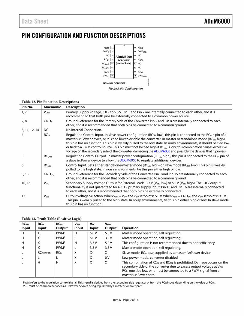
PIN CONFIGURATION AND FUNCTION DESCRIPTIONS
VDD1 1
GND1 2
NC 3
RCIN 4
VISO16
GNDISO15
NC14
VSEL13
RCOUT 5 NC12
RCSEL 6 NC
NC = NO CONNECT
11
VDD1 7 VISO10
GND1 8 GNDISO9
ADuM6000TOP VIEW
(Not to Scale)
0862
4-00
3
Figure 3. Pin Configuration
Table 12. Pin Function Descriptions Pin No. Mnemonic Description 1, 7 VDD1 Primary Supply Voltage, 3.0 V to 5.5 V. Pin 1 and Pin 7 are internally connected to each other, and it is
recommended that both pins be externally connected to a common power source. 2, 8 GND1 Ground Reference for the Primary Side of the Converter. Pin 2 and Pin 8 are internally connected to each
other, and it is recommended that both pins be connected to a common ground. 3, 11, 12, 14 NC No Internal Connection. 4 RCIN Regulation Control Input. In slave power configuration (RCSEL low), this pin is connected to the RCOUT pin of a
master isoPower device, or it is tied low to disable the converter. In master or standalone mode (RCSEL high), this pin has no function. This pin is weakly pulled to the low state. In noisy environments, it should be tied low or tied to a PWM control source. This pin must not be tied high if RCSEL is low; this combination causes excessive voltage on the secondary side of the converter, damaging the ADuM6000 and possibly the devices that it powers.
5 RCOUT Regulation Control Output. In master power configuration (RCSEL high), this pin is connected to the RCIN pin of a slave isoPower device to allow the ADuM6000 to regulate additional devices.
6 RCSEL Control Input. Sets either standalone/master mode (RCSEL high) or slave mode (RCSEL low). This pin is weakly pulled to the high state. In noisy environments, tie this pin either high or low.
9, 15 GNDISO Ground Reference for the Secondary Side of the Converter. Pin 9 and Pin 15 are internally connected to each other, and it is recommended that both pins be connected to a common ground.
10, 16 VISO Secondary Supply Voltage Output for External Loads. 3.3 V (VSEL low) or 5.0 V (VSEL high). The 5.0 V output functionality is not guaranteed for a 3.3 V primary supply input. Pin 10 and Pin 16 are internally connected to each other, and it is recommended that both pins be externally connected.
13 VSEL Output Voltage Selection. When VSEL = VISO, the VISO setpoint is 5.0 V. When VSEL = GNDISO, the VISO setpoint is 3.3 V. This pin is weakly pulled to the high state. In noisy environments, tie this pin either high or low. In slave mode, this pin has no function.
Table 13. Truth Table (Positive Logic) RCSEL Input
RCIN Input
RCOUT Output
VSEL Input
VDD1 Input
VISO Output Operation
H X PWM1 H 5.0 V 5.0 V Master mode operation, self regulating. H X PWM1 L 5.0 V 3.3 V Master mode operation, self regulating. H X PWM1 H 3.3 V 5.0 V This configuration is not recommended due to poor efficiency. H X PWM1 L 3.3 V 3.3 V Master mode operation, self regulating. L RCOUT(EXT) RCIN X X2 X Slave mode, RCOUT(EXT) supplied by a master isoPower device. L L L X X 0 V Low power mode, converter disabled. L H H X X X This combination of RCIN and RCSEL is prohibited. Damage occurs on the
secondary side of the converter due to excess output voltage at VISO. RCIN must be low, or it must be connected to a PWM signal from a master isoPower part.
1 PWM refers to the regulation control signal. This signal is derived from the secondary side regulator or from the RCIN input, depending on the value of RCSEL. 2 VDD1 must be common between all isoPower devices being regulated by a master isoPower part.
ADuM6000 Data Sheet
Rev. D | Page 10 of 16
TYPICAL PERFORMANCE CHARACTERISTICS
0862
4-00
40
5
10
15
20
25
30
35
0 20 40 60 80 100 120
EFFI
CIE
NCY
(%)
IISO CURRENT (mA)
5.0V INPUT/5.0V OUTPUT5.0V INPUT/3.3V OUTPUT3.3V INPUT/3.3V OUTPUT
Figure 4. Typical Power Supply Efficiency
in All Supported Power Configurations
120
100
80
60
40
20
00 50 100 150 200 250 300
IDD1 CURRENT (mA)
I ISO
CU
RR
ENT
(mA
)
0862
4-00
5
5.0V INPUT/5.0V OUTPUT5.0V INPUT/3.3V OUTPUT3.3V INPUT/3.3V OUTPUT
Figure 5. Typical Isolated Output Supply Current vs. Input Current
in All Supported Power Configurations
IISO CURRENT (mA)
TOTA
L PO
WER
DIS
SIPA
TIO
N (m
W)
0862
4-12
20
100
200
400
600
800
300
500
700
900
1000
0 20 40 60 80 100 120
5.0V INPUT/5.0V OUTPUT5.0V INPUT/3.3V OUTPUT3.3V INPUT/3.3V OUTPUT
Figure 6. Typical Total Power Dissipation vs. Isolated Output Supply Current
in All Supported Power Configurations
0
0.5
1.0
1.5
2.0
3.0
2.5
3.5
0
0.5
1.0
1.5
2.0
3.0
2.5
3.5
3.0 3.5 4.0 4.5 5.0 5.5 6.0INPUT SUPPLY VOLTAGE (V)
INPU
T C
UR
REN
T (A
)
POW
ER (W
)
POWER
IDD1
0862
4-00
6
Figure 7. Typical Short-Circuit Input Current and Power
vs. VDD1 Supply Voltage
TIME (ms)0
40
4.6
4.8
5.0
5.2
5.4
20
00.5 1.0 1.5 2.0 2.5 3.0 3.5 4.0
V ISO
(V)
I ISO
(mA
)
0862
4-00
7
10% LOAD
90% LOAD
10% LOAD
Figure 8. Typical VISO Transient Load Response, 5 V Output,
10% to 90% Load Step
TIME (ms)0
40
60
3.1
3.3
3.5
3.7
20
00.5 1.0 1.5 2.0 2.5 3.0 3.5 4.0
V ISO
(V)
I ISO
(mA
)
0862
4-00
8
10% LOAD
90% LOAD
10% LOAD
Figure 9. Typical VISO Transient Load Response, 3.3 V Output,
10% to 90% Load Step
Data Sheet ADuM6000
Rev. D | Page 11 of 16
TIME (µs)
RC
OU
T (V
)V I
SO (V
)
5.02
5.00
4.98
4.96
4.94
4.92
4.90
5.0
2.5
00 0.5 1.0 1.5 2.0 2.5 3.0 3.5 4.0
0862
4-00
9
Figure 10. Typical Output Voltage Ripple at 90% Load, VISO = 5 V
TIME (µs)
RC
OU
T (V
)V I
SO (V
)
3.34
3.30
3.32
3.28
3.26
3.244
2
0862
4-01
000 0.5 1.0 1.5 2.0 2.5 3.0 3.5 4.0
Figure 11. Typical Output Voltage Ripple at 90% Load, VISO = 3.3 V
0
1
2
3
4
5
6
7
–1.0 –0.5 0 0.5 1.0 1.5 2.0 2.5 3.0
V ISO
(V)
TIME (ms)
90% LOAD10% LOAD
0862
4-01
2
Figure 12. Typical Output Voltage Start-Up Transient at 10% and 90% Load, VISO = 5 V
0
1
2
3
4
5
–1.0 –0.5 0 0.5 1.0 1.5 2.0 2.5 3.0
V ISO
(V)
Time (ms)
90% LOAD10% LOAD
0862
4-01
3
Figure 13. Typical Output Voltage Start-Up Transient at 10% and 90% Load, VISO = 3.3 V

ADuM6000 Data Sheet
Rev. D | Page 12 of 16
APPLICATIONS INFORMATION The dc-to-dc converter section of the ADuM6000 works on principles that are common to most switching power supplies. It has a secondary side controller architecture with isolated pulse-width modulation (PWM) feedback. VDD1 power is supplied to an oscillating circuit that switches current into a chip scale air core transformer. Power transferred to the secondary side is rectified and regulated to either 3.3 V or 5 V. The secondary (VISO) side controller regulates the output by creating a PWM control signal that is sent to the primary (VDD1) side by a dedicated iCoupler data channel. The PWM modulates the oscillator circuit to control the power being sent to the secondary side. Feedback allows for significantly higher power and efficiency.
The ADuM6000 provides a regulation control output (RCOUT) signal that can be connected to other isoPower devices. This feature allows a single regulator to control multiple power mod-ules without contention. When auxiliary power modules are present, the VISO pins can be connected together to work as a single supply. Because there is only one feedback control path, the supplies work together seamlessly. The ADuM6000 can be a source of regulation control (master mode), and it can also be controlled by another isoPower device (slave mode).
The ADuM6000 implements undervoltage lockout (UVLO) with hysteresis in the VDD1 input protection circuitry. When the input voltage rises above the UVLO threshold, the dc-to-dc converter becomes active. The input voltage must be decreased below the turn-on threshold by the hysteresis value to disable the converter. This feature has many benefits in the power-up sequence of the converter. For example, UVLO ensures that the system supply rises to a minimum level before the ADuM6000 demands current. Also, it prevents any voltage drop due to converter current from turning the supply off and causing oscillation.
PCB LAYOUT The ADuM6000 digital isolator is a 0.4 W isoPower integrated dc-to-dc converter that requires no external interface circuitry for the logic interfaces. Power supply bypassing is required at the input and output supply pins (see Figure 14).
The power supply section of the ADuM6000 uses a 180 MHz oscillator frequency to pass power efficiently through its chip scale transformers. In addition, the normal operation of the data section of the iCoupler introduces switching transients on the power supply pins. Bypass capacitors are required for several operating frequencies. Noise suppression requires a low inductance, high frequency capacitor, whereas ripple suppression and proper regulation require a large value capacitor. These capacitors are most conveniently connected between Pin 1 and Pin 2 for VDD1, and between Pin 15 and Pin 16 for VISO.
To suppress noise and reduce ripple, a parallel combination of at least two capacitors is required. The recommended capacitor values are 0.1 μF and 10 μF. Best practice recommends using a very low inductance ceramic capacitor, or its equivalent, for the smaller value. The total lead length between both ends of the capacitor and the input power supply pin should not exceed 10 mm. Consider bypassing between Pin 1 and Pin 8 and between Pin 9 and Pin 16 unless both common ground pins are connected together close to the package.
VDD1GND1
NCRCIN
VISOGNDISO
NC
NC
NC
VSELRCOUTRCSEL
VDD1 VISOGND1 GNDISO
0862
4-01
1
Figure 14. Recommended PCB Layout
In applications involving high common-mode transients, ensure that board coupling across the isolation barrier is minimized. Furthermore, design the board layout such that any coupling that does occur affects all pins equally on a given component side. Failure to ensure this can cause voltage differentials between pins exceeding the absolute maximum ratings for the device as specified in Table 10, thereby leading to latch-up and/or permanent damage.
The ADuM6000 is a power device that dissipates approximately 1 W of power when fully loaded. Because it is not possible to apply a heat sink to an isolation device, the device primarily depends on heat dissipation into the PCB through the GND pins. If the device is used at high ambient temperatures, provide a thermal path from the GND pins to the PCB ground plane. The board layout in Figure 14 shows enlarged pads for Pin 2 and Pin 8 (GND1) and for Pin 9 and Pin 15 (GNDISO). Implement multiple vias from the pad to the ground plane to significantly reduce the temperature inside the chip. The dimensions of the expanded pads are at the discretion of the designer and depend on the available board space.
START-UP BEHAVIOR The ADuM6000 device does not contain a soft start circuit. Therefore, the start-up current and voltage behavior must be taken into account when designing with this device.
When power is applied to VDD1, the input switching circuit begins to operate and draw current when the UVLO minimum voltage is reached. The switching circuit drives the maximum available power to the output until it reaches the regulation voltage where PWM control begins. The amount of current and the time required to reach regulation voltage depends on the load and the VDD1 slew rate.

Data Sheet ADuM6000
Rev. D | Page 13 of 16
With a fast VDD1 slew rate (200 µs or less), the peak current draws up to 100 mA/V of VDD1. The input voltage goes high faster than the output can turn on, so the peak current is proportional to the maximum input voltage.
With a slow VDD1 slew rate (in the millisecond range), the input voltage is not changing quickly when VDD1 reaches the UVLO minimum voltage. The current surge is approximately 300 mA because VDD1 is nearly constant at the 2.7 V UVLO voltage. The behavior during startup is similar to when the device load is a short circuit; these values are consistent with the short-circuit current shown in Figure 7.
When starting the device for VISO = 5 V operation, do not limit the current available to the VDD1 power pin to less than 300 mA. The ADuM6000 device may not be able to drive the output to the regulation point if a current-limiting device clamps the VDD1 voltage during startup. As a result, the ADuM6000 device can draw large amounts of current at low voltage for extended periods of time.
The output voltage of the ADuM6000 device exhibits VISO overshoot during startup. If this overshoot could potentially damage components attached to VISO, a voltage-limiting device such as a Zener diode can be used to clamp the voltage. Typical behavior is shown in Figure 12 and Figure 13.
EMI CONSIDERATIONS The dc-to-dc converter section of the ADuM6000 must operate at 180 MHz to allow efficient power transfer through the small transformers. This creates high frequency currents that can propagate in circuit board ground and power planes, causing edge emissions and dipole radiation between the primary and secondary ground planes. Grounded enclosures are recommended for applications that use these devices. If grounded enclosures are not possible, follow good RF design practices in the layout of the PCB. See the AN-0971 Application Note for board layout recommendations.
THERMAL ANALYSIS The ADuM6000 consists of four internal silicon die attached to a split lead frame with two die attach paddles. For the purposes of thermal analysis, it is treated as a thermal unit with the highest junction temperature reflected in the θJA value from Table 5. The value of θJA is based on measurements taken with the part mounted on a JEDEC standard 4-layer board with fine width traces and still air. Under normal operating conditions, the ADuM6000 operates at full load across the full temperature range without derating the output current. However, following the recommendations in the PCB Layout section decreases the thermal resistance to the PCB, allowing increased thermal margin at high ambient temperatures.
CURRENT LIMIT AND THERMAL OVERLOAD PROTECTION The ADuM6000 is protected against damage due to excessive power dissipation by thermal overload protection circuits. Thermal overload protection limits the junction temperature to a maximum of 150°C (typical). Under extreme conditions (that is, high ambient temperature and power dissipation), when the junction temperature starts to rise above 150°C, the PWM is turned off, turning off the output current. When the junction temperature drops below 130°C (typical), the PWM turns on again, restoring the output current to its nominal value.
Consider the case where a hard short from VISO to ground occurs. At first, the ADuM6000 reaches its maximum current, which is proportional to the voltage applied at VDD1. Power dissipates on the primary side of the converter (see Figure 7). If self-heating of the junction becomes great enough to cause its temperature to rise above 150°C, thermal shutdown is activated, turning off the PWM and turning off the output current. As the junction temperature cools and drops below 130°C, the PWM turns on and power dissipates again on the primary side of the converter, causing the junction temperature to rise to 150°C again. This thermal oscillation between 130°C and 150°C causes the part to cycle on and off as long as the short remains at the output.
Thermal limit protections are intended to protect the device against accidental overload conditions. For reliable operation, externally limit device power dissipation to prevent junction temperatures from exceeding 130°C.
POWER CONSIDERATIONS The ADuM6000 converter primary side is protected from pre-mature operation by undervoltage lockout (UVLO) circuitry. Below the minimum operating voltage, the power converter holds its oscillator inactive.
When the primary side oscillator begins to operate, it transfers power to the secondary power circuits. The secondary VISO voltage starts below its UVLO limit, making it inactive and unable to generate a regulation control signal. The primary side power oscillator is allowed to free run under this condition, supplying the maximum amount of power to the secondary side.
As the secondary side voltage rises to its regulation setpoint, a large inrush current transient is present at VDD1. When the regula-tion point is reached, the regulation control circuit produces the regulation control signal that modulates the oscillator on the primary side. The VDD1 current is then reduced and is propor-tional to the load current. The inrush current is less than the short-circuit current shown in Figure 7. The duration of the inrush current depends on the VISO loading conditions and on the current and voltage available at the VDD1 pin.

ADuM6000 Data Sheet
Rev. D | Page 14 of 16
INCREASING AVAILABLE POWER The ADuM6000 device is designed to work in combination with other compatible isoPower devices. The RCOUT, RCIN, and RCSEL pins allow the ADuM6000 to provide its PWM signal to another device through its RCOUT pin, acting as a master. It can also receive a PWM signal from another device through its RCIN pin and act as a slave to that control signal. The RCSEL pin chooses whether the part acts as a master or slave device.
When the ADuM6000 acts as a slave, its power is regulated by the master device, allowing multiple isoPower parts to be combined in parallel while sharing the load equally. When the ADuM6000 is configured as a master or standalone device, it generates its own PWM feedback signal to regulate itself and any slave devices.
The ADuM6000 can function as a master, slave, or standalone device. All devices in the ADuM5xxx and ADuM6xxx family can function as standalone devices. Some of these devices also function as master devices or slave devices, but not both (see Table 14).
Table 15 illustrates how isoPower devices can provide many combinations of data channel count and multiples of the single-unit power.
Table 14. Function of isoPower Parts
Part No. Function
Master Slave Standalone ADuM6000 Yes Yes Yes ADuM620x No Yes Yes ADuM640x No No Yes ADuM5000 Yes Yes Yes ADuM520x No Yes Yes ADuM5400 No No Yes ADuM5401 to ADuM5404
Yes No Yes
Another feature that is allowed by the RCSEL and RCIN control architecture is the ability to completely shut down the oscillator in the dc-to-dc converter. This places the part in a low power standby mode and reduces the current draw to a fraction of a milliamp.
When the ADuM6000 is placed in slave mode by driving RCSEL low, the oscillator is controlled by RCIN. If RCIN is held low, the oscillator is shut down and the part is in low power standby mode. With no oscillator driving power to the secondary side, VISO turns off. This mode is useful for applications where an isolated subsystem may be shut down to conserve power. To reactivate the power module, drive RCSEL high; the power supply resumes operation.
Table 15. Configurations for Power and Data Channels
Power Units Number of Data Channels
0 Channels 2 Channels 4 Channels 1-Unit Power ADuM6000 or ADuM5000 (standalone) ADuM620x or ADuM520x (standalone) ADuM5401, ADuM5402, ADuM5403,
ADuM5404, or ADuM640x (standalone) 2-Unit Power ADuM6000 or ADuM5000 (master)
ADuM6000 or ADuM5000 (slave) ADuM6000 or ADuM5000 (master) ADuM620x or ADuM520x (slave)
ADuM5401, ADuM5402, ADuM5403, ADuM5404 (master)
ADuM6000 or ADuM5000 (slave) 3-Unit Power ADuM6000 or ADuM5000 (master) ADuM6000 or ADuM5000 (master) ADuM6000 or ADuM5000 (master)
ADuM6000 or ADuM5000 (slave) ADuM6000 or ADuM5000 (slave) ADuM620x or ADuM520x (slave) ADuM6000 or ADuM5000 (slave) ADuM620x or ADuM520x (slave) ADuM620x or ADuM520x (slave)

Data Sheet ADuM6000
Rev. D | Page 15 of 16
INSULATION LIFETIME All insulation structures eventually break down when subjected to voltage stress over a sufficiently long period. The rate of insu-lation degradation is dependent on the characteristics of the voltage waveform applied across the insulation. In addition to the testing performed by the regulatory agencies, Analog Devices carries out an extensive set of evaluations to determine the life-time of the insulation structure within the ADuM6000.
Analog Devices performs accelerated life testing using voltage levels higher than the rated continuous working voltage. Accel-eration factors for several operating conditions are determined. These factors allow calculation of the time to failure at the actual working voltage. The values shown in Table 11 summarize the peak voltage for 50 years of service life for a bipolar ac operating condition and the maximum CSA/VDE approved working volt-ages. In many cases, the approved working voltage is higher than the 50-year service life voltage. Operation at these high working voltages can lead to shortened insulation life in some cases.
The insulation lifetime of the ADuM6000 depends on the voltage waveform imposed across the isolation barrier. The iCoupler insulation structure degrades at different rates depend-ing on whether the waveform is bipolar ac, unipolar ac, or dc. Figure 15, Figure 16, and Figure 17 illustrate these different isolation voltage waveforms.
Bipolar ac voltage is the most stringent environment. The goal of a 50-year operating lifetime under the bipolar ac condition determines the maximum working voltage recommended by Analog Devices.
In the case of unipolar ac or dc voltage, the stress on the insu-lation is significantly lower. This allows operation at higher working voltages while still achieving a 50-year service life. The working voltages listed in Table 11 can be applied while maintaining the 50-year minimum lifetime, provided that the voltage conforms to either the unipolar ac or dc voltage cases.
Any cross-insulation voltage waveform that does not conform to Figure 16 or Figure 17 should be treated as a bipolar ac wave-form and its peak voltage limited to the 50-year lifetime voltage value listed in Table 11. The voltage presented in Figure 16 is shown as sinusoidal for illustration purposes only. It is meant to represent any voltage waveform varying between 0 V and some limiting value. The limiting value can be positive or negative, but the voltage cannot cross 0 V.
0V
RATED PEAK VOLTAGE
0862
4-02
1
Figure 15. Bipolar AC Waveform
0V
RATED PEAK VOLTAGE
0862
4-02
2
Figure 16. Unipolar AC Waveform
0V
RATED PEAK VOLTAGE
0862
4-02
3
Figure 17. DC Waveform

ADuM6000 Data Sheet
Rev. D | Page 16 of 16
OUTLINE DIMENSIONS
CONTROLLING DIMENSIONS ARE IN MILLIMETERS; INCH DIMENSIONS(IN PARENTHESES) ARE ROUNDED-OFF MILLIMETER EQUIVALENTS FORREFERENCE ONLY AND ARE NOT APPROPRIATE FOR USE IN DESIGN.
COMPLIANT TO JEDEC STANDARDS MS-013-AA
10.50 (0.4134)10.10 (0.3976)
0.30 (0.0118)0.10 (0.0039)
2.65 (0.1043)2.35 (0.0925)
10.65 (0.4193)10.00 (0.3937)
7.60 (0.2992)7.40 (0.2913)
0.75 (0.0295)0.25 (0.0098) 45°
1.27 (0.0500)0.40 (0.0157)
COPLANARITY0.10 0.33 (0.0130)
0.20 (0.0079)0.51 (0.0201)0.31 (0.0122)
SEATINGPLANE
8°0°
16 9
81
1.27 (0.0500)BSC
03-2
7-20
07-B
Figure 18. 16-Lead Standard Small Outline Package [SOIC_W]
Wide Body (RW-16)
Dimensions shown in millimeters and (inches)
11-1
5-20
11-A
16 9
81
SEATINGPLANE
COPLANARITY0.1
1.27 BSC
12.8512.7512.65
7.607.507.40
2.642.542.44
1.010.760.51
0.300.200.10
10.5110.3110.11
0.460.36
2.442.24
PIN 1MARK
1.93 REF
8°0°
0.320.23
0.710.500.31
45°0.25 BSC GAGEPLANE
COMPLIANT TO JEDEC STANDARDS MS-013-AC Figure 19. 16-Lead Standard Small Outline Package, with Increased Creepage [SOIC_IC]
Wide Body (RI-16-2)
Dimensions shown in millimeters
ORDERING GUIDE Model1 Temperature Range Package Description2 Package Option ADuM6000ARWZ −40°C to +105°C 16-Lead SOIC_W RW-16 ADuM6000ARIZ −40°C to +105°C 16-Lead SOIC_IC RI-16-2 1 Z = RoHS Compliant Part. 2 Tape and reel are available. The additional -RL suffix designates a 13-inch (1,000 units) tape and reel option.
©2010–2013 Analog Devices, Inc. All rights reserved. Trademarks and registered trademarks are the property of their respective owners. D08624-0-7/13(D)