ads794xevm and ads794xevm-pdk user guide · 9 ni-visadriver installation prompt ... • easily...
TRANSCRIPT

User's GuideSBAU194–August 2011
ADS794xEVM and ADS794xEVM-PDK
ADS794xEVM-PDK
This user's guide describes the characteristics, operation, and use of the ADS794xEVM by itself and aspart of the ADS794xEVM-PDK kit. These evaluation modules (EVMs) allow evaluation of all aspects ofeither the ADS7946 or ADS7945 devices (ADS794x). Both devices are 14-bit, dual-channel,ultralow-power, differential successive-approximation-register (SAR) analog-to-digital converters (ADCs)with a maximum throughput rate of 2 MSPS. The ADS7945 offers fully-differential input voltages while thepseudo-differential inputs of the ADS7946 offer single-ended input voltages with small common-modenoise-cancelling capabilities. Complete circuit descriptions, schematic diagrams, and bill of materials areincluded in this document.
The following related documents are available through the Texas Instruments web site athttp://www.ti.com.
Related Documentation
Device Literature Number
ADS7945SBAS539
ADS7946
OPA350 SBOS099C
OPA836 SLOS712B
REF5040 SBOS410E
SN74LVC2G74 SCES203M
ADCPro is a trademark of Texas Instruments.Microsoft, Windows are registered trademarks of Microsoft Corporation.SPI is a trademark of Motorola, Inc.I2C is a trademark of NXP Semiconductors.All other trademarks are the property of their respective owners.
1SBAU194–August 2011 ADS794xEVM and ADS794xEVM-PDKSubmit Documentation Feedback
Copyright © 2011, Texas Instruments Incorporated
www.ti.com
Contents1 EVM Overview ............................................................................................................... 32 Analog Interface ............................................................................................................. 43 Digital Interface .............................................................................................................. 74 Power Supplies .............................................................................................................. 85 EVM Operation .............................................................................................................. 96 ADS794xEVM-PDK: Software Installation ............................................................................. 107 ADS794xEVM-PDK Kit Operation ....................................................................................... 178 Bill of Materials, Schematics, and Layout .............................................................................. 20
List of Figures
1 ADS794xEVM and ADS7945 Analog Inputs ............................................................................ 5
2 ADS794xEVM and ADS7946 Analog Inputs ............................................................................ 6
3 ADS794xEVM Default Jumper Locations .............................................................................. 10
4 ADS794xEVM-PDK Plug-In Installer.................................................................................... 11
5 Completed ADS794xEVM-PDK Installer ............................................................................... 11
6 MMB0 Jumper Locations ................................................................................................. 12
7 Connecting ADS794xEVM to MMB0.................................................................................... 13
8 Powering Up ADS794xEVM-PDK ....................................................................................... 14
9 NI-VISA Driver Installation Prompt ...................................................................................... 15
10 Loading ADS794xEVM Plug-in From ADCPro ........................................................................ 15
11 USBStyx Driver Installation Prompt ..................................................................................... 16
12 ADS794xEVM Plug-in: Device Configuration Tab .................................................................... 18
13 ADCPro Test Plug-ins .................................................................................................... 19
14 ADS794xEVM PCB: Top Layer.......................................................................................... 22
15 ADS794xEVM PCB: Ground Layer ..................................................................................... 22
16 ADS794xEVM PCB: Power Layer....................................................................................... 23
17 ADS794xEVM PCB: Bottom Layer...................................................................................... 23
List of Tables
1 P2: Analog Interface Pinout (Samtec 10 x 2) ........................................................................... 4
2 SMA Analog Inputs ......................................................................................................... 4
3 P1: Serial Interface Header................................................................................................ 7
4 P3 Configuration: Power-Supply Interface Header ..................................................................... 8
5 ADS794xEVM Bill of Materials .......................................................................................... 20
2 ADS794xEVM and ADS794xEVM-PDK SBAU194–August 2011Submit Documentation Feedback
Copyright © 2011, Texas Instruments Incorporated

www.ti.com EVM Overview
1 EVM Overview
1.1 Features
ADS794xEVM Features:• Contains all support circuitry needed for the ADS7946/ADS7945 (ADS794x)
• 5-V, 3.3-V, and 1.8-V logic compatible with 16-bit, 40-MHz SPI™ serial interface
• Simple channel selection with a single 16-bit word command
• Serial interface header for easy connection to TI DSP-based communication systems
• Compatible with the TI Modular EVM System
• Voltage reference options: onboard REF5040 (4.096-V) reference or external reference
• Voltage reference buffering with OPA350
• Onboard OPA836 (200-MHz BW, 1-mA quiescent current) ADC input drivers
• Jumper-selectable bipolar (–VREF/2 to +VREF/2) or unipolar (0 V to VREF) input range
ADS794xEVM-PDK Features:• Easy-to-use evaluation software for Microsoft® Windows® XP operating system PCs
• Data collection to text files
• Built-in analysis tools including scope, FFT, and histogram displays
• Complete control of board settings
• Easily expandable with new analysis plug-in tools from Texas Instruments
The ADS794xEVM-PDK is available for use with a computer. This kit combines the ADS794xEVM boardwith the DSP-based MMB0 motherboard, and includes ADCPro™ software for evaluation.
The MMB0 motherboard allows the ADS794xEVM to be connected to the computer via an available USBport. This manual shows how to use the MMB0 as part of the ADS794xEVM-PDK, but does not providetechnical details about the MMB0 itself.
ADCPro is a program for collecting, recording, and analyzing data from ADC evaluation boards. It is basedon a number of plug-in programs, so it can be expanded easily with new test and data collection plug-ins.The ADS794xEVM-PDK is controlled by a plug-in running in ADCPro. For more information aboutADCPro, see the ADCPro™ Analog-to-Digital Converter Evaluation Software User's Guide (literaturenumber SBAU128), available for download from the TI web site.
This manual covers the operation of both the ADS794xEVM and the ADS794xEVM-PDK. Throughout thisdocument, the abbreviation EVM and the term evaluation module are synonymous with the ADS794xEVM.Operation of the EVM and kit for both the ADS7946 and the ADS7945 devices is identical, unlessotherwise noted.
1.2 Introduction
The ADS794xEVM is an evaluation module built to the TI Modular EVM System specifications. It can beconnected to any modular EVM system interface card.
The ADS794xEVM is available as a stand-alone printed circuit board (PCB) or as part of theADS794xEVM-PDK, which includes an MMB0 motherboard and software. As a stand-alone PCB, theADS794xEVM is useful for prototyping designs and firmware because it offers circuitry that meets theproduct data sheet specifications of either the ADS7946 or ADS7945 devices.
The ADS7945 and ADS7946 are 14-bit, 2-MSPS ADCs with fully differential and pseudo-differentialunipolar inputs, respectively. These devices operate at a 2-MSPS sample rate with a 16-clock SPI dataframe that features both outstanding dc and excellent dynamic performance. These devices also include atwo-channel input multiplexer and a low-power SAR ADC with an inherent sample-and-hold (S/H) inputstage. During normal operation at 2 MSPS, the ADS794x dissipates a mere 11.6 mW.
Note that the ADS794xEVM has no microprocessor and cannot run software. Therefore, some type ofinterface is required to connect the ADS794xEVM to a computer. In the ADS794xEVM-PDK kit, the MMB0motherboard serves as the interface between the computer and the ADS794xEVM board.
3SBAU194–August 2011 ADS794xEVM and ADS794xEVM-PDKSubmit Documentation Feedback
Copyright © 2011, Texas Instruments Incorporated

Analog Interface www.ti.com
2 Analog Interface
The ADS794xEVM is designed for easy interfacing to multiple analog sources. SMA connectors allow theEVM to have input signals connected via coaxial cables. In addition, the Samtec connector provides aconvenient 10-pin, dual-row, header/socket combination at P2. This header/socket provides access to theanalog input pins of the ADS794x. Consult Samtec at http://www.samtec.com or call 1-800-SAMTEC-9 fora variety of mating connector options. All analog inputs are buffered by OPA836 high-speed operationalamplifiers in order to properly drive the ADS794x ADC inputs.
Use appropriate caution when handling these pins. Table 1 summarizes the pinout for analog interface P2.
Table 1. P2: Analog Interface Pinout (Samtec 10 x 2)
Pin Number Signal Description
CH0 positive differential input for ADS7945; open ifP2.2 A0(+) / OPEN ADS7946 is installed
CH0 negative differential input for ADS7945;P2.4 A0(–) single-ended input for ADS7946
CH1 positive differential input for ADS7945; open ifP2.10 A1(+) / OPEN ADS7946 is installed
CH1 negative differential input for ADS7945;P2.12 A1(–) single-ended input for ADS7946
P2.1-19 (odd) GND Analog ground connections (except J1.15)
P2.6 and P2.8 GND Analog ground connections
P2.14, P2.16, and P2.18 GND Analog ground connections
Unbuffered output. VREF/4 (J6 open) or VREF/2 (J6P2.15 VREF/4 or VREF/2 closed)
P2.20 Ext VREF External reference voltage input
Table 2 lists the SMA analog inputs.
Table 2. SMA Analog Inputs
Pin Number Signal Description
CH0 positive differential input for ADS7945; noJ10 A0(+) / No SMA SMA if ADS7946 is installed
CH0 negative differential input for ADS7945;J11 A0(–) single-ended input for ADS7946
CH1 positive differential input for ADS7945; noJ4 A1(+) / No SMA SMA if ADS7946 is installed
CH1 negative differential input for ADS7945;J5 A1(–) single-ended input for ADS7946
As noted in Table 1 and Table 2, there are different hardware configurations depending on the installedconverter. The ADS7945 uses two inputs per channel because of its fully differential inputs. The ADS7946uses one input per channel for its pseudo-differential inputs.
4 ADS794xEVM and ADS794xEVM-PDK SBAU194–August 2011Submit Documentation Feedback
Copyright © 2011, Texas Instruments Incorporated
4
10
12
SMA
J10
SMA
J11
SMA
J4
SMA
J5
A0(+)
A1(+)
A0( )-
A1( )-
OPA836 in Inverting
Configuration
OPA836 in Inverting
Configuration
OPA836 in Inverting
Configuration
OPA836 in Inverting
Configuration
P2
AIN1P (pin 8)
AIN1N (pin 7)
AIN0P (pin 5)
AIN0N (pin 6)
ADS7945
www.ti.com Analog Interface
2.1 ADS794xEVM Analog Inputs with ADS7945 Installed
Each channel of the ADS7945 uses two OPA836 operational amplifiers to drive the fully differential inputs.The input signals can be applied to either the SMA or P2 header connectors. These operational amplifiersoffset the input signal to use an inverting configuration with a single supply. The EVM Operation sectionexplains in detail how this offset is used to allow bipolar signals for the ADS7945 with jumper J6.
Figure 1 illustrates the ADS794xEVM analog inputs with the ADS7945 installed.
Figure 1. ADS794xEVM and ADS7945 Analog Inputs
5SBAU194–August 2011 ADS794xEVM and ADS794xEVM-PDKSubmit Documentation Feedback
Copyright © 2011, Texas Instruments Incorporated

4
10
12
No SMA
J10
SMA
J11
No SMA
J4
SMA
J5
A0(+)
A1(+)
A0( )-
A1( )-
OPA836 in Inverting
Configuration
OPA836 in Inverting
Configuration
P2
AIN1P (pin 8)
AIN1N (pin 7)
AIN0P (pin 5)
AIN0N (pin 6)
ADS7946
Open
Open
Analog Interface www.ti.com
2.2 ADS794xEVM Analog Inputs with ADS7946 Installed
Each channel of the ADS7946 uses one OPA836 to drive a single-ended input voltage. The input signalscan be applied to either the SMA or P2 header connectors. These operational amplifiers offset the inputsignal to use an inverting configuration with a single supply. The EVM Operation section explains in detailhow this offset is used to allow bipolar signals for the ADS7946 with jumper J6.
Figure 2 shows the ADS794xEVM analog inputs with the ADS7946 installed.
Figure 2. ADS794xEVM and ADS7946 Analog Inputs
2.3 External Reference Input
Pin P2.20 is an analog input for an external reference voltage when J2 is in position 2-3. The source thatprovides this external reference should have a voltage between 2.5 V and the analog power-supplyvoltage.
6 ADS794xEVM and ADS794xEVM-PDK SBAU194–August 2011Submit Documentation Feedback
Copyright © 2011, Texas Instruments Incorporated
www.ti.com Digital Interface
3 Digital Interface
Samtec part numbers SSW-110-22-F-D-VS-K and TSM-110-01-L-DV-P provide a convenient 10-pin,dual-row, header/socket combination at P1. This header/socket provides access to the digital control pinsof the ADC. Consult Samtec at http://www.samtec.com or call 1-800-SAMTEC-9 for a variety of matingconnector options.
Table 3 summarizes the pinouts for digital interface P1.
Table 3. P1: Serial Interface Header
Pin Number Signal Description
P1.1 CS Chip select input. Pulled high with 10-kΩ resistor.
P1.3 SCLK Serial clock input
Chip select input. This pin is intended to be used byP1.7 CS the MMB0 motherboard
P1.11 SDI or MOSI SDI or MOSI input
P1.13 SDO or MISO SDO or MISO output
Power-down input (active high). Pulled down withP1.19 PDEN 10-kΩ resistor.
P1.4, P1.10, and P1.18 GND Digital ground connections
I2C bus; used only used to program the U4P1.16, P1.20 I2C™ bus EEPROM on the EVM board
P1.2, P1.5-6, P1.8-9,P1.12, P1.14-15, and Unused Unused
P1.17
3.1 Serial Interface (SPI)
The ADS794x ADC uses SPI serial communication in mode 0 (CPOL = 0, CPHA = 0). Because the serialclock (SCLK) frequency can be as fast as 40 MHz, the ADS794xEVM offers 47-Ω resistors between theSPI signals and P1 to aid with signal integrity. Typically, in high-speed SPI communication, fast signaledges can cause overshoot; these 47-Ω resistors slow down the signal edges in order to minimize signalovershoot.
3.2 ADS794x Channel Select as SDI (MISO)
The ADS794x ADC offers direct control over the internal multiplexer using pin 11. The ADS794xEVM usesa flip-flop (see U9 in the attached schematic) to convert this pin into a typical SPI SDI (MOSI) pin. Thisarchitecture takes advantage of the SPI full-duplex data transmission sequence to control channelselection at the same time conversion data are acquired. The digital word 0x000 can be used to selectchannel 0, and the word 0xFFFF can be used to select channel 1.
3.3 I2C Bus for Onboard EEPROM
The ADS794xEVM has an I2C bus to communicate with the onboard EEPROM that records the boardname and assembly date. It is not used in any form by the ADS794x converter.
7SBAU194–August 2011 ADS794xEVM and ADS794xEVM-PDKSubmit Documentation Feedback
Copyright © 2011, Texas Instruments Incorporated
Power Supplies www.ti.com
4 Power Supplies
P3 is the power-supply input connector. Table 4 lists the configuration details for P3.
Table 4. P3 Configuration: Power-Supply Interface Header
Pin Number Pin Name Function Required
P3.3 +5VA 5-V analog supply Yes
P3.5 GND Digital ground input Yes
P3.6 GND Analog ground input Yes
P3.7 +1.8VD 1.8-V digital supply Yes/Optional
P3.9 +3.3VD 3.3-V digital supply Yes/Optional
P3.10 +5VD 5-V digital supply Yes/Optional
P3.1-2, P3.4, and Unused Unused NoP3.7-8
4.1 Analog Power Options
The ADS794xEVM board is designed to work with a 5-V analog power supply connected to P3.3.
4.2 Digital Power Options
The ADS794xEVM uses a jumper in J3 to connect the digital power supply to either +3.3 VD (P3.10) or +5VD (P3.9). J3 in position 1-2 connects the digital power supply to +5 VD; position 2-3 connects the digitalpower supply to +3.3 VD. Without a jumper in J3, the digital power supply can be connected to +1.8VD(P3.7) with a jumper wire to pin J3.2. The jumper in J3 must always be in position 2-3 (+3.3 VD) whileusing the MMB0 with the EVM.
4.3 Reference Voltages
The ADS794xEVM uses a jumper in J2 to select between the internal (REF5040) and external voltagereference sources. J2 in position 1-2 selects the internal reference; position 2-3 selects the externalreference. The selected reference is cleaned with a RC filter and buffered with a OPA350 operationalamplifier.
CAUTION
Digital supply and reference voltage must be at or below the analog supplyvoltage at all times.
8 ADS794xEVM and ADS794xEVM-PDK SBAU194–August 2011Submit Documentation Feedback
Copyright © 2011, Texas Instruments Incorporated

www.ti.com EVM Operation
5 EVM Operation
This section provides information on the analog input, digital control, and general operating conditions ofthe ADS794xEVM without the MMB0 motherboard. Software operation is presented in Section 7.
5.1 Analog Input
The ADS794xEVM offers three different analog input modes, selectable with jumper J6 and the type ofinput signal. Note that the ADS794x converter by itself only allows dc-coupled unipolar signals. The twoadditional input modes are available because OPA836 operational amplifiers drive the analog inputs. It ispreferable for external signal drivers or filters to have low output impedance to reduce gain errors.
Mode 1: DC-Coupled Unipolar Inputs (J6 Closed)
DC-coupled unipolar signals are typically produced by single-supply signal drivers. To allow dc-coupledunipolar signals, J6 should be closed. This mode allows an input signal range from 0 V to VREF for all EVManalog inputs. In this mode, the voltage read at the ADC is equal to (VREF – VIN).
Mode 2: DC-Coupled Bipolar Inputs (J6 Open)
DC-coupled bipolar signals are typically produced by dual-supply signal drivers. To allow dc-coupledbipolar signals, J6 should be open. This mode allows an input signal range from –VREF/2 to +VREF/2 for allEVM analog inputs. In this mode, the voltage read at the ADC is equal to (VREF/2 – VIN).
Mode 3: AC-Coupled Inputs (J6 Closed)
AC-coupled signals are typically produced by high-pass filters. To allow ac-coupled bipolar signals, J6should be closed. This mode allows an input signal range from –VREF/2 to +VREF/2 for all EVM analoginputs. In this mode, the voltage read at the ADC is equal to (VREF/2 – VIN).
5.2 Digital Control
The digital control signals can be applied directly to the P1 header (top or bottom side). The modularADS794xEVM can also be connected directly to a DSP or microcontroller interface board, such as the5-6K Interface or HPA-MCU Interface boards available from Texas Instruments, or the MMB0 if purchasedas part of the ADS794xEVM-PDK. For a list of compatible interface and/or accessory boards for the EVMor the ADS794x, see the relevant product folder on the TI web site.
9SBAU194–August 2011 ADS794xEVM and ADS794xEVM-PDKSubmit Documentation Feedback
Copyright © 2011, Texas Instruments Incorporated

ADS794xEVM-PDK: Software Installation www.ti.com
5.3 Default Jumper Settings
Figure 3 shows the jumper locations on the EVM board and the respective factory default conditions foreach.
Figure 3. ADS794xEVM Default Jumper Locations
There are four jumpers on the ADS794xEVM board. These jumpers are used to set the CS signal entrypin (J1), select the digital logic level (J3), select the reference (J2), and to establish the input signal rangetype (J6). The default parameters are:
• The CS signal entry pin is P1.7 (J1: 2-3).
• The logic level is 3.3 V (J3: 2-3).
• The onboard 4.096 V is selected as the reference voltage (J1: 1-2).
• Analog input range is 0 V to VREF (4.096 V) with dc-coupled signals (J6: closed)
6 ADS794xEVM-PDK: Software Installation
This section presents the steps required to the install the software. Section 7 explains how to operate thesoftware to acquire data.
Complete the following steps to install the software:
Step 1. Install the ADCPro software (if not already installed) on a PC.
Step 2. Install the ADS794xEVM-PDK EVM plug-in software.
Step 3. Set up the ADS794xEVM-PDK hardware.
Step 4. Power up the ADS794xEVM-PDK.
Step 5. Connect the ADS794xEVM-PDK to the computer with a USB cable.
Step 6. Complete the USB driver installation process.
Each task is described in the subsequent sections of this document.
10 ADS794xEVM and ADS794xEVM-PDK SBAU194–August 2011Submit Documentation Feedback
Copyright © 2011, Texas Instruments Incorporated

www.ti.com ADS794xEVM-PDK: Software Installation
6.1 Installing the ADCPro Software
CAUTION
Do not connect the ADS794xEVM-PDK to a PC before completing Section 6.2through Section 6.4. Failure to observe this caution may cause MicrosoftWindows to not recognize the ADS794xEVM-PDK as a connected device.
ADCPro is the primary program used to evaluate ADCs. The latest software version of ADCPro isavailable from the TI website at www.ti.com. Refer to the ADCPro User Guide for instructions on installingand using ADCPro.
6.2 Installing ADS794xEVM-PDK Plug-In Software
The ADS794xEVM-PDK plug-in uses ADCPro; you must install ADCPro before uploading the plug-in.
To install the ADS794xEVM-PDK plug-in, run the file: ads794X-adcproplugin-<version #>.exe (<version#> refers to the installation file version number, and increments with software version releases).Double-click the file to run it; then follow the instructions as shown. You can also use the ADCPro UpdateCheck feature to check for newer versions of the ADS794xEVM-PDK plug-in, once you have installed aversion of it.
Figure 4 and Figure 5 show the initial and completed installer screenshots, respectively.
Figure 4. ADS794xEVM-PDK Plug-In Installer
Figure 5. Completed ADS794xEVM-PDK Installer
11SBAU194–August 2011 ADS794xEVM and ADS794xEVM-PDKSubmit Documentation Feedback
Copyright © 2011, Texas Instruments Incorporated

ADS794xEVM-PDK: Software Installation www.ti.com
6.3 Configuring the ADS794xEVM-PDK Hardware
The ADS794xEVM-PDK contains both the ADS794xEVM and the MMB0 motherboard; however, thedevices may be shipped unconnected or configured incorrectly. Follow these steps to verify thatADS794xEVM-PDK kit is properly configured and connected.
Step 1. Unpack the ADS794xEVM-PDK kit.
Step 2. Set the three jumpers on the MMB0 REV D as shown in Figure 6. Below Figure 6, there is acheck list that explains the functionality of each jumper.
Figure 6. MMB0 Jumper Locations
Follow this check list to ensure proper operation of the MMB0 with the ADS794xEVM:
• J12 must be closed. This setting allows the wall supply to power up the MMB0 and theADS794xEVM through J2 (6-VDC input), and regulate down to +5 V, 3.3 V, and 1.8 V.
• J13B must be closed. This configuration connects the 5-V analog power supply with the 5-V digitalpower supply.
• J13A must be opened. This setting allows the 5-V analog power supply to be regulated onboard.
12 ADS794xEVM and ADS794xEVM-PDK SBAU194–August 2011Submit Documentation Feedback
Copyright © 2011, Texas Instruments Incorporated

www.ti.com ADS794xEVM-PDK: Software Installation
Step 3. Plug the ADS794xEVM into the MMB0, as Figure 7 illustrates.
Figure 7. Connecting ADS794xEVM to MMB0
CAUTION
Do not misalign the pins when plugging the ADS794xEVM into the MMB0.Check the pin alignment carefully before applying power to the PDK.
Step 4. Set jumper J3 on the ADS794xEVM to position 2-3 in order to set the ADS794xEVM logicvoltage to 3.3 V. The MMB0 uses 3.3-V logic to communicate with the ADS7945xEVM.
Step 5. Set jumper J1 on the ADS794xEVM to position 2-3 in order to place the CS signal in P1.7 ofthe EVM. The MMB0 sends the CS signal via P1.7.
Step 6. Set jumper J2 on the ADS794xEVM to position 1-2 if the 4.096-V internal (onboard) referenceis used. If an external reference is used, set J2 to the 2-3 position.
CAUTION
If an external reference is used, please do not apply external reference voltagebefore the power is applied to the MMB0 motherboard.
Step 7. Set jumper J6 to match the correct type of input signal, as explained in Section 5.1:
• For dc-coupled unipolar input signals, J6 must be closed.
• For dc-oupled bipolar input signals, J6 must be opened.
• For ac-coupled signals, J6 must be closed.
13SBAU194–August 2011 ADS794xEVM and ADS794xEVM-PDKSubmit Documentation Feedback
Copyright © 2011, Texas Instruments Incorporated

ADS794xEVM-PDK: Software Installation www.ti.com
6.4 Powering Up the ADS794xEVM-PDK
Once the ADS794xEVM-PDK kit is configured, power can be applied to the MMB0. This power comesfrom a wall supply that delivers +6 VDC to the MMB0 via J2 on the MMB0 motherboard. This wall powersupply is included with the PDK; it should be connected where Figure 8 indicates.
Figure 8. Powering Up ADS794xEVM-PDK
After the power supply is connected, four green LEDs in the bottom right-hand corner of the MMB0motherboard should light up. If these LEDs do not light up, disconnect the power and verify that J12 isclosed.
6.5 First-Time Connection: ADS794xEVM-PDK to PC, Completing Driver Installation
The first time that the ADS794xEVM-PDK kit is connected to the PC via USB, the PC prompts the user fortwo drivers. At this point, it is presumed that the ADCPro software and the ADS794xEVM plug-in havebeen installed, and that the ADS794xEVM-PDK kit is properly configured and powered up (refer toSection 6.1 through Section 6.4). The following sections show how to install these drivers.
NOTE: Driver prompts may not appear if another PDK kit has been used on the PC before.
14 ADS794xEVM and ADS794xEVM-PDK SBAU194–August 2011Submit Documentation Feedback
Copyright © 2011, Texas Instruments Incorporated
www.ti.com ADS794xEVM-PDK: Software Installation
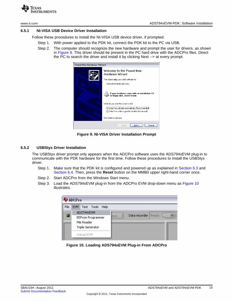
6.5.1 NI-VISA USB Device Driver Installation
Follow these procedures to install the NI-VISA USB device driver, if prompted.
Step 1. With power applied to the PDK kit, connect the PDK kit to the PC via USB.
Step 2. The computer should recognize the new hardware and prompt the user for drivers, as shownin Figure 9. This driver should be present in the PC hard drive with the ADCPro files. Directthe PC to search the driver and install it by clicking Next --> at every prompt.
Figure 9. NI-VISA Driver Installation Prompt
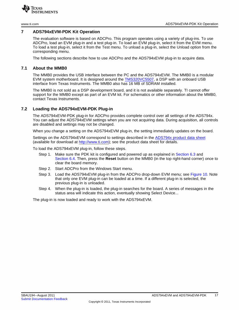
6.5.2 USBStyx Driver Installation
The USBStyx driver prompt only appears when the ADCPro software uses the ADS794xEVM plug-in tocommunicate with the PDK hardware for the first time. Follow these procedures to install the USBStyxdriver.
Step 1. Make sure that the PDK kit is configured and powered up as explained in Section 6.3 andSection 6.4. Then, press the Reset button on the MMB0 upper right-hand corner once.
Step 2. Start ADCPro from the Windows Start menu.
Step 3. Load the ADS794xEVM plug-in from the ADCPro EVM drop-down menu as Figure 10illustrates.
Figure 10. Loading ADS794xEVM Plug-in From ADCPro
15SBAU194–August 2011 ADS794xEVM and ADS794xEVM-PDKSubmit Documentation Feedback
Copyright © 2011, Texas Instruments Incorporated

ADS794xEVM-PDK: Software Installation www.ti.com
Step 4. Wait for the driver prompt window to appear. When the plug-in is first loaded, the plug-insearches for the board. You will see a series of messages in the status area indicating thisaction; eventually, the driver prompt window will appear, as Figure 11 shows.
Figure 11. USBStyx Driver Installation Prompt
NOTE: If the USBStyx driver was previously installed on the PC, the status area should show themessage Select Device without prompting for the driver. If this message appears, closeADCpro and proceed to Section 7.
Step 5. This driver should be present in the PC hard drive with the ADCPro files. Direct the PC tosearch the driver and install it by clicking Next --> at every prompt. Be patient; it may takesome time for the PC to find the driver.
NOTE: During the driver installation, a small pop-up window may appear indicating that the firmwareload has timed out. Ignore this pop-up. Continue with the USBStyx driver installation. Oncedriver installation has finished, click the Exit button in the small-pop up window.
Step 6. Close ADCPro after the USBStyx driver has been installed.
16 ADS794xEVM and ADS794xEVM-PDK SBAU194–August 2011Submit Documentation Feedback
Copyright © 2011, Texas Instruments Incorporated
www.ti.com ADS794xEVM-PDK Kit Operation
7 ADS794xEVM-PDK Kit Operation
The evaluation software is based on ADCPro. This program operates using a variety of plug-ins. To useADCPro, load an EVM plug-in and a test plug-in. To load an EVM plug-in, select it from the EVM menu.To load a test plug-in, select it from the Test menu. To unload a plug-in, select the Unload option from thecorresponding menu.
The following sections describe how to use ADCPro and the ADS794xEVM plug-in to acquire data.
7.1 About the MMB0
The MMB0 provides the USB interface between the PC and the ADS794xEVM. The MMB0 is a modularEVM system motherboard. It is designed around the TMS320VC5507, a DSP with an onboard USBinterface from Texas Instruments. The MMB0 also has 16 MB of SDRAM installed.
The MMB0 is not sold as a DSP development board, and it is not available separately. TI cannot offersupport for the MMB0 except as part of an EVM kit. For schematics or other information about the MMB0,contact Texas Instruments.
7.2 Loading the ADS794xEVM-PDK Plug-in
The ADS794xEVM-PDK plug-in for ADCPro provides complete control over all settings of the ADS794x.You can adjust the ADS794xEVM settings when you are not acquiring data. During acquisition, all controlsare disabled and settings may not be changed.
When you change a setting on the ADS794xEVM plug-in, the setting immediately updates on the board.
Settings on the ADS794xEVM correspond to settings described in the ADS794x product data sheet(available for download at http://www.ti.com); see the product data sheet for details.
To load the ADS794xEVM plug-in, follow these steps.
Step 1. Make sure the PDK kit is configured and powered up as explained in Section 6.3 andSection 6.4. Then, press the Reset button on the MMB0 (in the top right-hand corner) once toclear the board memory.
Step 2. Start ADCPro from the Windows Start menu.
Step 3. Load the ADS794xEVM plug-in from the ADCPro drop-down EVM menu; see Figure 10. Notethat only one EVM plug-in can be loaded at a time. If a different plug-in is selected, theprevious plug-in is unloaded.
Step 4. When the plug-in is loaded, the plug-in searches for the board. A series of messages in thestatus area will indicate this action, eventually showing Select Device...
The plug-in is now loaded and ready to work with the ADS794xEVM.
17SBAU194–August 2011 ADS794xEVM and ADS794xEVM-PDKSubmit Documentation Feedback
Copyright © 2011, Texas Instruments Incorporated

ADS794xEVM-PDK Kit Operation www.ti.com
7.3 Using the ADS794xEVM Plug-in
The ADS794xEVM plug-in allows the user to evaluate the ADS794x ADC. Figure 12 shows the deviceconfiguration tab of the ADS794xEVM Plug-in. Use this tab of the ADCPro software to configure theADS794x.
Figure 12. ADS794xEVM Plug-in: Device Configuration Tab
The device configuration tab contains the following controls.
(1) Device Selection: This control is a user input that must be set by the user, to identify whether theADS7945 or ADS7946 is installed on the board.
(2) Channel Select: This user input selects the channel to be sampled.
(3) Data Rate: This control shows the data rate or sampling frequency used by the ADC to acquire data.
(4) Power Down: This option controls the power-down mode of the ADC.
(5) Device Interface Information: This option shows the SPI parameters that are in use while samplingdata. These parameters should appear after a device is selected.
(6) About: This control shows the plug-in version, MMB0 firmware version, ADS794xEVM assembly date,and ADS794xEVM board revision information. This information should appear after a device is selected.
(7) Collection Bar: This feature shows the percentage of data collected during an acquisition session.
18 ADS794xEVM and ADS794xEVM-PDK SBAU194–August 2011Submit Documentation Feedback
Copyright © 2011, Texas Instruments Incorporated

www.ti.com ADS794xEVM-PDK Kit Operation
7.4 Loading the Test Plug-in
Once the ADS794xEVM plug-in is configured in ADCPro, one of the four test plug-ins must be loaded inADCPro using the drop-down Test menu, as shown in Figure 13. Note that only one Test plug-in can beloaded at a time. If a different plug-in is selected, the previous plug-in is unloaded.
Figure 13. ADCPro Test Plug-ins
There are four different test options available for the ADS794xEVM:
• Data monitor: This test acquires data and exports it in table format as hexadecimal data.
• MultiFFT: This test allows the user to acquire data and create an FFT graph of power vs. frequency todisplay data
• MultiHistogram: This option acquires data and creates a histogram of code values.
• MultiScope: This feature acquires data and displays it in a graph of voltage vs. time.
For further details regarding how to set up and use the various test plug-ins, refer to the ADCPro UserGuide.
7.5 Acquiring Data
Once the ADS794xEVM is configured for the desired test scenario, press the Acquire button to start thedata collection process; the software collects the number of data points specified in the Test plug-in BlockSize control. While acquiring data, the ADS794xEVM plug-in disables all front panel controls, and thecollection process bar displays the completion progress.
7.6 Troubleshooting
If the ADS794xEVM plug-in cannot find the ADS794xEVM-PDK, press the RESET button on the MMB0and try again.
If ADCPro stops responding while the ADS794xEVM-PDK is connected, shut down and restart theADCPro software. Also, try unplugging the USB cable from the PDK. Unload and reload the plug-in beforereapplying power to the PDK.
19SBAU194–August 2011 ADS794xEVM and ADS794xEVM-PDKSubmit Documentation Feedback
Copyright © 2011, Texas Instruments Incorporated
Bill of Materials, Schematics, and Layout www.ti.com
8 Bill of Materials, Schematics, and Layout
Schematics for the ADS794xEVM are appended to this user's guide. The bill of materials is provided inTable 5. Section 8.2 shows the PCB layouts for the ADS794xEVM.
8.1 Bill of Materials
NOTE: All components should be compliant with the European Union Restriction on Use ofHazardous Substances (RoHS) Directive. Some part numbers may be either leaded orRoHS. Verify that purchased components are RoHS-compliant. (For more information aboutTI's position on RoHS compliance, see the http://www.ti.com.)
Table 5. ADS794xEVM Bill of Materials
Qty
Item No. ADS7945 ADS7946 Ref Des Description Vendor Part Number
Texas1 1 1 N/A Printed Circuit Board 6527650Instruments
C1, C13, C17,4 4 Capacitor, X7R Ceramic ±10%,C242 Murata GRM188R71C104KA01D16WV, 06032 0 C20, C23
C2, C4, C10, Capacitor, X7R Ceramic ±10%,3 4 4 TDK C1608X7R1A105KC14 10WV, 0603
Capacitor, X7R Ceramic ±20%,4 2 2 C3, C11 Taiyo Yuden JMK316B7226ML-T6.3WV, 1206
Capacitor, X7R Ceramic ±10%,5 3 3 C5, C6, C29 Taiyo Yuden JMK212B7106KG-T6.3WV, 0805
Capacitor, X7R Ceramic ±10%,6 1 1 C8 Murata GRM188R71A225KE15D10WV, 0603
C9, C12, C16,6 6 Capacitor, C0G Ceramic ±5%,C26, C27, C287 Murata GRM1885C1H102JA01D50WV, 06032 0 C22, C25
2 2 C15, C19 Capacitor, C0G Ceramic ±0.1p,8 TDK C1608C0G1H2R2B50WV, 06032 0 C18, C21
Header, 20-Pin SMT Plug, .100"9 2 2 P1A, P2A Samtec TSM-110-01-L-DV-PGold (2x10)
Header, 20-pin SMT Socket, .100"10 2 2 P1B, P2B Samtec SSW-110-22-F-D-VS-KGold (2x10)
Header, 10-Pin SMT Plug, .100"11 1 1 P3A Samtec TSM-105-01-L-DV-PGold (2x5)
Header, 10-pin SMT Socket, .100"12 1 1 P3B Samtec SSW-105-22-F-D-VS-KGold (2x5)
Header, Strip, 3-pin .100" Gold13 3 3 J1, J2, J3 Samtec TSW-103-07-L-S(1x3)
2 2 J5, J11 Amphenol 13213414 Connector, SMA Jack Straight PCB
2 0 J4, J10 Emerson 142-0701-201
15 1 1 J6 Header Strip, 2-pin .100" Gold (1x2) Samtec TSW-102-07-L-S
R1, R2, R3, R4,8 8 R8, R28, R31, Resistor, Thick Film Chip, 1%,16 Panasonic ERJ-3EKF47R0VR42 1/10W, 06032 0 R34, R37
Resistor, Metal Film Chip, 0.1%,17 1 1 R14 Panasonic ERA-6AEB302V1/8W, 0805
Resistor, Metal Film Chip, 0.1%,18 1 1 R30 Panasonic ERA-6AEB152V1/8W, 0805
Resistor, Metal Film Chip, 0.1%,19 1 1 R15 Panasonic ERA-6AEB102V1/8W, 0805
Resistor, Metal Film Chip, 0.1%,20 1 1 R11 Panasonic ERA-3AEB102V1/10W, 0603
Resistor, Thick Film Chip, 1%,21 2 2 R5, R6 Panasonic ERJ-3EKF1002V1/10W, 0603
20 ADS794xEVM and ADS794xEVM-PDK SBAU194–August 2011Submit Documentation Feedback
Copyright © 2011, Texas Instruments Incorporated

www.ti.com Bill of Materials, Schematics, and Layout
Table 5. ADS794xEVM Bill of Materials (continued)
Qty
Item No. ADS7945 ADS7946 Ref Des Description Vendor Part Number
R20, R21, R26, Resistor, Thick Film Chip, 1%,22 4 4 Vishay/Dale CRCW06034R99FKEAR27 1/10W, 0603
R16, R17, R24,4 4 R45 Resistor, Metal Film Chip, 0.1%,23 Panasonic ERA-3AEB103V1/10W, 0603R18, R22, R23,4 0 R39
3 3 R32, R40, R46 Resistor, Thick Film Chip, 1%,24 Vishay/Dale CRCW06031R00FKEA1/10W, 06032 0 R35, R38
2 2 R9, R12 Resistor, Thick Film Chip, 1/10W,25 Panasonic ERJ-3GEY0R00V06030 2 R25, R29
26 3 3 T1, T2, T4 Test point PC Mini .040" D Red Keystone 5000
27 3 3 T5, T6, T7 Test point PC Mini .040" D Black Keystone 5001
28 1 1 T8 Test point PC Mini .040" D Yellow Keystone 5004
IC ADC, 14-bit, 2.5 MSPS, Full-Diff, Texas1 0 ADS7945SRTEQFN-16 Instruments29 U1
IC ADC, 14-bit, 2.5 MSPS, Texas0 1 ADS7946SRTEPseudo-Diff, QFN-16 Instruments
IC Prec Volt Ref, 4.096 V LN/LD Texas30 1 1 U2 REF5040IDGKT8-MSOP Instruments
IC Op Amp, GP, R-R 38 MHz Texas31 1 1 U3 OPA350EA/250Single, 8-MSOP Instruments
IC EEPROM, 256kBit, 400 kHz,32 1 1 U4 Microchip 24LC256-I/ST8-TSSOP
Texas33 1 1 U9 IC D-Type, F-F w/CLR Preset SM8 SN74LVC2G74DCTRInstruments
2 2 U5, U8 IC Op Amp, R-R Out, 200 MHz, Texas34 OPA836IDBVTSOT-23 Instruments2 0 U6, U7
35 4 4 N/A 0.100 Shunt, Black 3M 969102-0000-DA
21SBAU194–August 2011 ADS794xEVM and ADS794xEVM-PDKSubmit Documentation Feedback
Copyright © 2011, Texas Instruments Incorporated

Bill of Materials, Schematics, and Layout www.ti.com
8.2 Board Layouts
Figure 14 through Figure 17 show the PCB layouts for the ADS794xEVM.
NOTE: Board layouts are not to scale. These figures are intended to show how the board is laid out;they are not intended to be used for manufacturing ADS794xEVM PCBs.
Figure 14. ADS794xEVM PCB: Top Layer
Figure 15. ADS794xEVM PCB: Ground Layer
22 ADS794xEVM and ADS794xEVM-PDK SBAU194–August 2011Submit Documentation Feedback
Copyright © 2011, Texas Instruments Incorporated

www.ti.com Bill of Materials, Schematics, and Layout
Figure 16. ADS794xEVM PCB: Power Layer
Figure 17. ADS794xEVM PCB: Bottom Layer
23SBAU194–August 2011 ADS794xEVM and ADS794xEVM-PDKSubmit Documentation Feedback
Copyright © 2011, Texas Instruments Incorporated

A
B
D
C
A
B
C
D
6 5 4 3 2 1
DATE:LTR ECO NO: APPROVED:
REVISION RECORD
DATED:
DESIGNED BY:
SIZE:
C
ADS7945-6EVM
/CS
FSX
SCLK
MOSI
MISO
/CS
SCLK
CH_SEL
SDO
GPIO5
EXT_REF_IN
SCLK
REF+
Texas Instruments, Inc.
HIGH-PERFORMANCE ANALOG DIVISIONPRECISION ANALOG PRODUCTS
SEMICONDUCTOR GROUP5411 EAST WILLIAMS BOULEVARD, TUCSON, AZ 85711 USA
TITLE:
May-17-2011REV:
A
DRAWN BY:
Rafael Ordonez
Rafael Ordonez
6527650DOCUMENT CONTROL NO.
SHEET OF1 1 FILE: ADS7945-6EVM_A.sch
6 5 4 3 2 1
REF IN/EXT
/CS or FSX
VD 5.0/3.3
Unipolar
AGND
AGND
AGND
+VD
+5VA
EXT_REF
UniPolar VCM_Ouput
CH_SEL
*
*
*
*
*
*
*
**
*
*
*
1 23 45 67 89 10
11 1213 1415 1617 1819 20
P2
1 23 45 67 89 10
11 1213 1415 1617 1819 20
P1
1 23 45 67 89 10
P3
1
GND
2
AVDD
3
REFP
4
REFN
5AIN0P
6AIN0N
7AIN1N
8AIN1P
9
NC
10
NC
11CH_SEL
12PDEN
13CS
14SCLK
15SDO
16DVDD
17
THERMAL_PAD
U1
ADS7945/6
2 VIN
3 TEMP
6VOUT
4GND
5TRIM
U2
REF5040
REF5040IDGKT 2
3
4
6
7U3
OPA350EA/250
1 A02 A13 A2
4GND
5SDA6SCL
7 WP
8VCC
U4
24LC256-I/ST
R1 47
R2 47
R3 47
R4 47
J1
R6 10k
C3
22u
C1 0.1u
C2 1u
R5 10k R7 NI
R8
47
R9 0
J2
C4
1u
R11 1k
C6
10u
R12 0
C8 2.2u
C9
1000p
C10
1u
J3
C11
22u
C12
1000p
C13 0.1u
C14
1u
R14
3k
R15
1k
1
2
3
4
5
6 U5
OPA836IDBVT
R16 10kR17 10k
C15 2.2p
C16
1000p
C17 0.1u
1
2
3
4
56 U6
OPA836IDBVT
R18 10k
C18 2.2p
C20 0.1u
R20 4.99
R21 4.99
1
2
3
4
56 U7
OPA836IDBVT
R22 10kR23 10k
C21 2.2p
C22
1000p
C23 0.1u
R26 4.99
R27 4.99
C27
1000p
C28
1000p
R28 47
1
2345
J10
1
2345
J11
T1
T2
T3
T4
T5
T6
T7
C5
10u
R10
NI
R19
NI
1
2
3
4
5
6U8
OPA836IDBVT
R24 10k
C19 2.2p
C24 0.1u
T8
R25 NI
R29 NI
R31 47
R32 1
R34 47R35 1
R37 47
C25
1000p
R38 1
R39 10k
R40 1
R42 47
C26
1000p
R43
NI
R44
NI
R45 10k
R46
1
C29
10u
1
2345
J4
1
2345
J5
1CLK
2D
3Q
4
GND
5Q
6
CLR
7
PRE
8
VC
C
U9
SN74LVC2G74DCTR
R30
1.5kJ6
+5VA
+VD
+3.3VD
+5VA
+3.3VD +5VD
+5VA
+VD
+5VD
+3.3VD
+5VA
+5VA
+5VA
+5VA
+5VA
+5VA
+VD
UN_POL_VCM
A0(+)
A0(-)
A0(+)
A0(-)
A1(+)
UN_POL_VCM
UN_POL_VCM
UN_POL_VCM
UN_POL_VCM
A1(-)
A0(+)
A0(-)
A1(-)
A1(+)
A1(+)A1(-)

Evaluation Board/Kit Important Notice
Texas Instruments (TI) provides the enclosed product(s) under the following conditions:
This evaluation board/kit is intended for use for ENGINEERING DEVELOPMENT, DEMONSTRATION, OR EVALUATIONPURPOSES ONLY and is not considered by TI to be a finished end-product fit for general consumer use. Persons handling theproduct(s) must have electronics training and observe good engineering practice standards. As such, the goods being provided arenot intended to be complete in terms of required design-, marketing-, and/or manufacturing-related protective considerations,including product safety and environmental measures typically found in end products that incorporate such semiconductorcomponents or circuit boards. This evaluation board/kit does not fall within the scope of the European Union directives regardingelectromagnetic compatibility, restricted substances (RoHS), recycling (WEEE), FCC, CE or UL, and therefore may not meet thetechnical requirements of these directives or other related directives.
Should this evaluation board/kit not meet the specifications indicated in the User’s Guide, the board/kit may be returned within 30days from the date of delivery for a full refund. THE FOREGOING WARRANTY IS THE EXCLUSIVE WARRANTY MADE BYSELLER TO BUYER AND IS IN LIEU OF ALL OTHER WARRANTIES, EXPRESSED, IMPLIED, OR STATUTORY, INCLUDINGANY WARRANTY OF MERCHANTABILITY OR FITNESS FOR ANY PARTICULAR PURPOSE.
The user assumes all responsibility and liability for proper and safe handling of the goods. Further, the user indemnifies TI from allclaims arising from the handling or use of the goods. Due to the open construction of the product, it is the user’s responsibility totake any and all appropriate precautions with regard to electrostatic discharge.
EXCEPT TO THE EXTENT OF THE INDEMNITY SET FORTH ABOVE, NEITHER PARTY SHALL BE LIABLE TO THE OTHERFOR ANY INDIRECT, SPECIAL, INCIDENTAL, OR CONSEQUENTIAL DAMAGES.
TI currently deals with a variety of customers for products, and therefore our arrangement with the user is not exclusive.
TI assumes no liability for applications assistance, customer product design, software performance, or infringement ofpatents or services described herein.
Please read the User’s Guide and, specifically, the Warnings and Restrictions notice in the User’s Guide prior to handling theproduct. This notice contains important safety information about temperatures and voltages. For additional information on TI’senvironmental and/or safety programs, please contact the TI application engineer or visit www.ti.com/esh.
No license is granted under any patent right or other intellectual property right of TI covering or relating to any machine, process, orcombination in which such TI products or services might be or are used.
FCC Warning
This evaluation board/kit is intended for use for ENGINEERING DEVELOPMENT, DEMONSTRATION, OR EVALUATIONPURPOSES ONLY and is not considered by TI to be a finished end-product fit for general consumer use. It generates, uses, andcan radiate radio frequency energy and has not been tested for compliance with the limits of computing devices pursuant to part 15of FCC rules, which are designed to provide reasonable protection against radio frequency interference. Operation of thisequipment in other environments may cause interference with radio communications, in which case the user at his own expensewill be required to take whatever measures may be required to correct this interference.
EVM Warnings and Restrictions
It is important to operate this EVM within the input voltage range of –5 V to +5 V and the output voltage range of 0 V to +5 V.
Exceeding the specified input range may cause unexpected operation and/or irreversible damage to the EVM. If there arequestions concerning the input range, please contact a TI field representative prior to connecting the input power.
Applying loads outside of the specified output range may result in unintended operation and/or possible permanent damage to theEVM. Please consult the EVM User's Guide prior to connecting any load to the EVM output. If there is uncertainty as to the loadspecification, please contact a TI field representative.
During normal operation, some circuit components may have case temperatures greater than +27°C. The EVM is designed tooperate properly with certain components above +60°C as long as the input and output ranges are maintained. These componentsinclude but are not limited to linear regulators, switching transistors, pass transistors, and current sense resistors. These types ofdevices can be identified using the EVM schematic located in the EVM User's Guide. When placing measurement probes nearthese devices during operation, please be aware that these devices may be very warm to the touch.
Mailing Address: Texas Instruments, Post Office Box 655303, Dallas, Texas 75265Copyright © 2011, Texas Instruments Incorporated

EVALUATION BOARD/KIT/MODULE (EVM) ADDITIONAL TERMSTexas Instruments (TI) provides the enclosed Evaluation Board/Kit/Module (EVM) under the following conditions:
The user assumes all responsibility and liability for proper and safe handling of the goods. Further, the user indemnifies TI from all claimsarising from the handling or use of the goods.
Should this evaluation board/kit not meet the specifications indicated in the User’s Guide, the board/kit may be returned within 30 days fromthe date of delivery for a full refund. THE FOREGOING LIMITED WARRANTY IS THE EXCLUSIVE WARRANTY MADE BY SELLER TOBUYER AND IS IN LIEU OF ALL OTHER WARRANTIES, EXPRESSED, IMPLIED, OR STATUTORY, INCLUDING ANY WARRANTY OFMERCHANTABILITY OR FITNESS FOR ANY PARTICULAR PURPOSE. EXCEPT TO THE EXTENT OF THE INDEMNITY SET FORTHABOVE, NEITHER PARTY SHALL BE LIABLE TO THE OTHER FOR ANY INDIRECT, SPECIAL, INCIDENTAL, OR CONSEQUENTIALDAMAGES.
Please read the User's Guide and, specifically, the Warnings and Restrictions notice in the User's Guide prior to handling the product. Thisnotice contains important safety information about temperatures and voltages. For additional information on TI's environmental and/or safetyprograms, please visit www.ti.com/esh or contact TI.
No license is granted under any patent right or other intellectual property right of TI covering or relating to any machine, process, orcombination in which such TI products or services might be or are used. TI currently deals with a variety of customers for products, andtherefore our arrangement with the user is not exclusive. TI assumes no liability for applications assistance, customer product design,software performance, or infringement of patents or services described herein.
REGULATORY COMPLIANCE INFORMATIONAs noted in the EVM User’s Guide and/or EVM itself, this EVM and/or accompanying hardware may or may not be subject to the FederalCommunications Commission (FCC) and Industry Canada (IC) rules.
For EVMs not subject to the above rules, this evaluation board/kit/module is intended for use for ENGINEERING DEVELOPMENT,DEMONSTRATION OR EVALUATION PURPOSES ONLY and is not considered by TI to be a finished end product fit for general consumeruse. It generates, uses, and can radiate radio frequency energy and has not been tested for compliance with the limits of computingdevices pursuant to part 15 of FCC or ICES-003 rules, which are designed to provide reasonable protection against radio frequencyinterference. Operation of the equipment may cause interference with radio communications, in which case the user at his own expense willbe required to take whatever measures may be required to correct this interference.
General Statement for EVMs including a radioUser Power/Frequency Use Obligations: This radio is intended for development/professional use only in legally allocated frequency andpower limits. Any use of radio frequencies and/or power availability of this EVM and its development application(s) must comply with locallaws governing radio spectrum allocation and power limits for this evaluation module. It is the user’s sole responsibility to only operate thisradio in legally acceptable frequency space and within legally mandated power limitations. Any exceptions to this are strictly prohibited andunauthorized by Texas Instruments unless user has obtained appropriate experimental/development licenses from local regulatoryauthorities, which is responsibility of user including its acceptable authorization.
For EVMs annotated as FCC – FEDERAL COMMUNICATIONS COMMISSION Part 15 Compliant
CautionThis device complies with part 15 of the FCC Rules. Operation is subject to the following two conditions: (1) This device may not causeharmful interference, and (2) this device must accept any interference received, including interference that may cause undesired operation.
Changes or modifications not expressly approved by the party responsible for compliance could void the user's authority to operate theequipment.
FCC Interference Statement for Class A EVM devicesThis equipment has been tested and found to comply with the limits for a Class A digital device, pursuant to part 15 of the FCC Rules.These limits are designed to provide reasonable protection against harmful interference when the equipment is operated in a commercialenvironment. This equipment generates, uses, and can radiate radio frequency energy and, if not installed and used in accordance with theinstruction manual, may cause harmful interference to radio communications. Operation of this equipment in a residential area is likely tocause harmful interference in which case the user will be required to correct the interference at his own expense.

FCC Interference Statement for Class B EVM devicesThis equipment has been tested and found to comply with the limits for a Class B digital device, pursuant to part 15 of the FCC Rules.These limits are designed to provide reasonable protection against harmful interference in a residential installation. This equipmentgenerates, uses and can radiate radio frequency energy and, if not installed and used in accordance with the instructions, may causeharmful interference to radio communications. However, there is no guarantee that interference will not occur in a particular installation. Ifthis equipment does cause harmful interference to radio or television reception, which can be determined by turning the equipment off andon, the user is encouraged to try to correct the interference by one or more of the following measures:
• Reorient or relocate the receiving antenna.• Increase the separation between the equipment and receiver.• Connect the equipment into an outlet on a circuit different from that to which the receiver is connected.• Consult the dealer or an experienced radio/TV technician for help.
For EVMs annotated as IC – INDUSTRY CANADA Compliant
This Class A or B digital apparatus complies with Canadian ICES-003.
Changes or modifications not expressly approved by the party responsible for compliance could void the user’s authority to operate theequipment.
Concerning EVMs including radio transmitters
This device complies with Industry Canada licence-exempt RSS standard(s). Operation is subject to the following two conditions: (1) thisdevice may not cause interference, and (2) this device must accept any interference, including interference that may cause undesiredoperation of the device.
Concerning EVMs including detachable antennasUnder Industry Canada regulations, this radio transmitter may only operate using an antenna of a type and maximum (or lesser) gainapproved for the transmitter by Industry Canada. To reduce potential radio interference to other users, the antenna type and its gain shouldbe so chosen that the equivalent isotropically radiated power (e.i.r.p.) is not more than that necessary for successful communication.
This radio transmitter has been approved by Industry Canada to operate with the antenna types listed in the user guide with the maximumpermissible gain and required antenna impedance for each antenna type indicated. Antenna types not included in this list, having a gaingreater than the maximum gain indicated for that type, are strictly prohibited for use with this device.
Cet appareil numérique de la classe A ou B est conforme à la norme NMB-003 du Canada.
Les changements ou les modifications pas expressément approuvés par la partie responsable de la conformité ont pu vider l’autorité del'utilisateur pour actionner l'équipement.
Concernant les EVMs avec appareils radio
Le présent appareil est conforme aux CNR d'Industrie Canada applicables aux appareils radio exempts de licence. L'exploitation estautorisée aux deux conditions suivantes : (1) l'appareil ne doit pas produire de brouillage, et (2) l'utilisateur de l'appareil doit accepter toutbrouillage radioélectrique subi, même si le brouillage est susceptible d'en compromettre le fonctionnement.
Concernant les EVMs avec antennes détachables
Conformément à la réglementation d'Industrie Canada, le présent émetteur radio peut fonctionner avec une antenne d'un type et d'un gainmaximal (ou inférieur) approuvé pour l'émetteur par Industrie Canada. Dans le but de réduire les risques de brouillage radioélectrique àl'intention des autres utilisateurs, il faut choisir le type d'antenne et son gain de sorte que la puissance isotrope rayonnée équivalente(p.i.r.e.) ne dépasse pas l'intensité nécessaire à l'établissement d'une communication satisfaisante.
Le présent émetteur radio a été approuvé par Industrie Canada pour fonctionner avec les types d'antenne énumérés dans le manueld’usage et ayant un gain admissible maximal et l'impédance requise pour chaque type d'antenne. Les types d'antenne non inclus danscette liste, ou dont le gain est supérieur au gain maximal indiqué, sont strictement interdits pour l'exploitation de l'émetteur.
SPACER
SPACER
SPACER
SPACER
SPACER
SPACER
SPACER
SPACER
【【Important Notice for Users of this Product in Japan】】This development kit is NOT certified as Confirming to Technical Regulations of Radio Law of Japan
If you use this product in Japan, you are required by Radio Law of Japan to follow the instructions below with respect to this product:
1. Use this product in a shielded room or any other test facility as defined in the notification #173 issued by Ministry of Internal Affairs andCommunications on March 28, 2006, based on Sub-section 1.1 of Article 6 of the Ministry’s Rule for Enforcement of Radio Law ofJapan,
2. Use this product only after you obtained the license of Test Radio Station as provided in Radio Law of Japan with respect to thisproduct, or
3. Use of this product only after you obtained the Technical Regulations Conformity Certification as provided in Radio Law of Japan withrespect to this product. Also, please do not transfer this product, unless you give the same notice above to the transferee. Please notethat if you could not follow the instructions above, you will be subject to penalties of Radio Law of Japan.
Texas Instruments Japan Limited(address) 24-1, Nishi-Shinjuku 6 chome, Shinjuku-ku, Tokyo, Japan
http://www.tij.co.jp
【ご使用にあたっての注】
本開発キットは技術基準適合証明を受けておりません。
本製品のご使用に際しては、電波法遵守のため、以下のいずれかの措置を取っていただく必要がありますのでご注意ください。1. 電波法施行規則第6条第1項第1号に基づく平成18年3月28日総務省告示第173号で定められた電波暗室等の試験設備でご使用いただく。2. 実験局の免許を取得後ご使用いただく。3. 技術基準適合証明を取得後ご使用いただく。
なお、本製品は、上記の「ご使用にあたっての注意」を譲渡先、移転先に通知しない限り、譲渡、移転できないものとします。
上記を遵守頂けない場合は、電波法の罰則が適用される可能性があることをご留意ください。
日本テキサス・インスツルメンツ株式会社東京都新宿区西新宿6丁目24番1号西新宿三井ビルhttp://www.tij.co.jp
SPACER
SPACER
SPACER
SPACER
SPACER
SPACER
SPACER
SPACER
SPACER
SPACER
SPACER
SPACER
SPACER
SPACER
SPACER
SPACER

EVALUATION BOARD/KIT/MODULE (EVM)WARNINGS, RESTRICTIONS AND DISCLAIMERS
For Feasibility Evaluation Only, in Laboratory/Development Environments. Unless otherwise indicated, this EVM is not a finishedelectrical equipment and not intended for consumer use. It is intended solely for use for preliminary feasibility evaluation inlaboratory/development environments by technically qualified electronics experts who are familiar with the dangers and application risksassociated with handling electrical mechanical components, systems and subsystems. It should not be used as all or part of a finished endproduct.
Your Sole Responsibility and Risk. You acknowledge, represent and agree that:
1. You have unique knowledge concerning Federal, State and local regulatory requirements (including but not limited to Food and DrugAdministration regulations, if applicable) which relate to your products and which relate to your use (and/or that of your employees,affiliates, contractors or designees) of the EVM for evaluation, testing and other purposes.
2. You have full and exclusive responsibility to assure the safety and compliance of your products with all such laws and other applicableregulatory requirements, and also to assure the safety of any activities to be conducted by you and/or your employees, affiliates,contractors or designees, using the EVM. Further, you are responsible to assure that any interfaces (electronic and/or mechanical)between the EVM and any human body are designed with suitable isolation and means to safely limit accessible leakage currents tominimize the risk of electrical shock hazard.
3. You will employ reasonable safeguards to ensure that your use of the EVM will not result in any property damage, injury or death, evenif the EVM should fail to perform as described or expected.
4. You will take care of proper disposal and recycling of the EVM’s electronic components and packing materials.
Certain Instructions. It is important to operate this EVM within TI’s recommended specifications and environmental considerations per theuser guidelines. Exceeding the specified EVM ratings (including but not limited to input and output voltage, current, power, andenvironmental ranges) may cause property damage, personal injury or death. If there are questions concerning these ratings please contacta TI field representative prior to connecting interface electronics including input power and intended loads. Any loads applied outside of thespecified output range may result in unintended and/or inaccurate operation and/or possible permanent damage to the EVM and/orinterface electronics. Please consult the EVM User's Guide prior to connecting any load to the EVM output. If there is uncertainty as to theload specification, please contact a TI field representative. During normal operation, some circuit components may have case temperaturesgreater than 60°C as long as the input and output are maintained at a normal ambient operating temperature. These components includebut are not limited to linear regulators, switching transistors, pass transistors, and current sense resistors which can be identified using theEVM schematic located in the EVM User's Guide. When placing measurement probes near these devices during normal operation, pleasebe aware that these devices may be very warm to the touch. As with all electronic evaluation tools, only qualified personnel knowledgeablein electronic measurement and diagnostics normally found in development environments should use these EVMs.
Agreement to Defend, Indemnify and Hold Harmless. You agree to defend, indemnify and hold TI, its licensors and their representativesharmless from and against any and all claims, damages, losses, expenses, costs and liabilities (collectively, "Claims") arising out of or inconnection with any use of the EVM that is not in accordance with the terms of the agreement. This obligation shall apply whether Claimsarise under law of tort or contract or any other legal theory, and even if the EVM fails to perform as described or expected.
Safety-Critical or Life-Critical Applications. If you intend to evaluate the components for possible use in safety critical applications (suchas life support) where a failure of the TI product would reasonably be expected to cause severe personal injury or death, such as deviceswhich are classified as FDA Class III or similar classification, then you must specifically notify TI of such intent and enter into a separateAssurance and Indemnity Agreement.
Mailing Address: Texas Instruments, Post Office Box 655303, Dallas, Texas 75265Copyright © 2012, Texas Instruments Incorporated

IMPORTANT NOTICE
Texas Instruments Incorporated and its subsidiaries (TI) reserve the right to make corrections, enhancements, improvements and otherchanges to its semiconductor products and services per JESD46, latest issue, and to discontinue any product or service per JESD48, latestissue. Buyers should obtain the latest relevant information before placing orders and should verify that such information is current andcomplete. All semiconductor products (also referred to herein as “components”) are sold subject to TI’s terms and conditions of salesupplied at the time of order acknowledgment.
TI warrants performance of its components to the specifications applicable at the time of sale, in accordance with the warranty in TI’s termsand conditions of sale of semiconductor products. Testing and other quality control techniques are used to the extent TI deems necessaryto support this warranty. Except where mandated by applicable law, testing of all parameters of each component is not necessarilyperformed.
TI assumes no liability for applications assistance or the design of Buyers’ products. Buyers are responsible for their products andapplications using TI components. To minimize the risks associated with Buyers’ products and applications, Buyers should provideadequate design and operating safeguards.
TI does not warrant or represent that any license, either express or implied, is granted under any patent right, copyright, mask work right, orother intellectual property right relating to any combination, machine, or process in which TI components or services are used. Informationpublished by TI regarding third-party products or services does not constitute a license to use such products or services or a warranty orendorsement thereof. Use of such information may require a license from a third party under the patents or other intellectual property of thethird party, or a license from TI under the patents or other intellectual property of TI.
Reproduction of significant portions of TI information in TI data books or data sheets is permissible only if reproduction is without alterationand is accompanied by all associated warranties, conditions, limitations, and notices. TI is not responsible or liable for such altereddocumentation. Information of third parties may be subject to additional restrictions.
Resale of TI components or services with statements different from or beyond the parameters stated by TI for that component or servicevoids all express and any implied warranties for the associated TI component or service and is an unfair and deceptive business practice.TI is not responsible or liable for any such statements.
Buyer acknowledges and agrees that it is solely responsible for compliance with all legal, regulatory and safety-related requirementsconcerning its products, and any use of TI components in its applications, notwithstanding any applications-related information or supportthat may be provided by TI. Buyer represents and agrees that it has all the necessary expertise to create and implement safeguards whichanticipate dangerous consequences of failures, monitor failures and their consequences, lessen the likelihood of failures that might causeharm and take appropriate remedial actions. Buyer will fully indemnify TI and its representatives against any damages arising out of the useof any TI components in safety-critical applications.
In some cases, TI components may be promoted specifically to facilitate safety-related applications. With such components, TI’s goal is tohelp enable customers to design and create their own end-product solutions that meet applicable functional safety standards andrequirements. Nonetheless, such components are subject to these terms.
No TI components are authorized for use in FDA Class III (or similar life-critical medical equipment) unless authorized officers of the partieshave executed a special agreement specifically governing such use.
Only those TI components which TI has specifically designated as military grade or “enhanced plastic” are designed and intended for use inmilitary/aerospace applications or environments. Buyer acknowledges and agrees that any military or aerospace use of TI componentswhich have not been so designated is solely at the Buyer's risk, and that Buyer is solely responsible for compliance with all legal andregulatory requirements in connection with such use.
TI has specifically designated certain components which meet ISO/TS16949 requirements, mainly for automotive use. Components whichhave not been so designated are neither designed nor intended for automotive use; and TI will not be responsible for any failure of suchcomponents to meet such requirements.
Products Applications
Audio www.ti.com/audio Automotive and Transportation www.ti.com/automotive
Amplifiers amplifier.ti.com Communications and Telecom www.ti.com/communications
Data Converters dataconverter.ti.com Computers and Peripherals www.ti.com/computers
DLP® Products www.dlp.com Consumer Electronics www.ti.com/consumer-apps
DSP dsp.ti.com Energy and Lighting www.ti.com/energy
Clocks and Timers www.ti.com/clocks Industrial www.ti.com/industrial
Interface interface.ti.com Medical www.ti.com/medical
Logic logic.ti.com Security www.ti.com/security
Power Mgmt power.ti.com Space, Avionics and Defense www.ti.com/space-avionics-defense
Microcontrollers microcontroller.ti.com Video and Imaging www.ti.com/video
RFID www.ti-rfid.com
OMAP Applications Processors www.ti.com/omap TI E2E Community e2e.ti.com
Wireless Connectivity www.ti.com/wirelessconnectivity
Mailing Address: Texas Instruments, Post Office Box 655303, Dallas, Texas 75265Copyright © 2012, Texas Instruments Incorporated

Mouser Electronics
Authorized Distributor
Click to View Pricing, Inventory, Delivery & Lifecycle Information: Texas Instruments:
ADS7945EVM-PDK