adrv-dpd1/pcbz small cell radio reference design … · adrv-dpd1/pcbz user guide ug-1238 rev. 0 |...
TRANSCRIPT

ADRV-DPD1/PCBZ User GuideUG-1238
One Technology Way • P.O. Box 9106 • Norwood, MA 02062-9106, U.S.A. • Tel: 781.329.4700 • Fax: 781.461.3113 • www.analog.com
ADRV-DPD1/PCBZ Small Cell Radio Reference Design with Digital Predistortion
PLEASE SEE THE LAST PAGE FOR AN IMPORTANT WARNING AND LEGAL TERMS AND CONDITIONS. Rev. A | Page 1 of 115
FEATURES Complete JESD204B to antenna port design with AD9375
DPD and SKY66297-11 PA 2 × 2 LTE 20 MHz, 250 mW output power per antenna, Band 7
FDD Contains transceiver, 2 PAs, 2 LNAs, duplex filters, and dc
power solution Power consumption of radio board: approximately 10 W Powered from single 12 V supply Evaluation kit connects to baseband subsystem
EVALUATION KIT CONTENTS ADRV-DPD1/PCBZ radio board ADRV-INTERPOS1/PCBZ interposer board with clock solution One 8 GB SD card RF adapters between series SMP (F) and SMA (F) 12 V, 60 W ac/dc external desktop (Class I) power supply
EQUIPMENT NEEDED EVAL-TPG-ZYNQ3 evaluation board for Xilinx Zynq-7000 FPGA Ethernet cable IEC C13 ac power cable (not included)
SOFTWARE NEEDED AD9375 Small Cell Radio Reference Design Evaluation
Software GUI
GENERAL DESCRIPTION The ADRV-DPD1/PCBZ is a 24 dBm per path, 2 × 2 multiple input, multiple output (MIMO) radio board, which uses the AD9375, a highly integrated radio frequency (RF) transceiver with integrated digital predistortion (DPD). The radio board is designed to be used with the dual connector interposer board to interface with the EVAL-TPG-ZYNQ3 or other Xilinx® or Avnet evaluation boards for the Xilinx Zynq™-7000 field programmable gate array (FPGA) platform, which has a dual core ARM Cortex®-A9 processor running a Linux® variant.
The AD9375 small cell evaluation software (SCES), AD9375 Small Cell Radio Reference Design Evaluation Software GUI, can configure and control the ADRV-DPD1/PCBZ board.
Note that the Mykonos transceiver evaluation software (MTES) and DPD graphical user interface (GUI) software are not com-patible with the ADRV-DPD1/PCBZ.
Full specifications on the AD9375 are available in the AD9375 data sheet available from Analog Devices, Inc., and must be consulted in conjunction with this user guide when using the evaluation board.

UG-1238 ADRV-DPD1/PCBZ User Guide
Rev. A | Page 2 of 115
TABLE OF CONTENTS Features .............................................................................................. 1 Evaluation Kit Contents ................................................................... 1 Equipment Needed ........................................................................... 1 Software Needed ............................................................................... 1 General Description ......................................................................... 1 Revision History ............................................................................... 3 ADRV-DPD1/PCBZ Evaluation Kit Photograph ......................... 4 Getting Started .................................................................................. 5
Software Installation .................................................................... 5 SCES Setup Requirements ........................................................... 5 SCES Setup .................................................................................... 5 Evaluation Kit Setup ..................................................................... 8
Hardware Operation ................................................................ 9 SCES Quickstart ......................................................................... 10
Basic Receiver Setup .............................................................. 10 Basic Transmitter Setup ......................................................... 10 Basic DPD Setup ..................................................................... 11
Evaluation Kit Hardware ............................................................... 12 Power Supply Connection ......................................................... 12 ADRV-DPD1/PCBZ Top and Bottom View Photographs.... 13 Interposer Board Reference ...................................................... 15 System Reference Clocks ........................................................... 15 LED Indicators ............................................................................ 15 ADP5054 Enable Jumper ........................................................... 16 EEPROM Write Protect Enable Headers ................................ 16 Debug Headers............................................................................ 17
RF A Header Pins ................................................................... 17 RF B Header Pins ................................................................... 17 JTAG Header Pins .................................................................. 18
SPI Chip Select Lines ................................................................. 18 Pin Configurations and Function Descriptions ......................... 20 Using the Software for Testing ...................................................... 30
Graphical User Interface Operation......................................... 30 Starting the AD9375 SCES ........................................................ 30
Demo Mode ............................................................................ 30 Normal Operation ...................................................................... 32
Software Update ..................................................................... 32 GUI Reference............................................................................. 33
Configuring the AD9375 ...................................................... 33 Configuration Tab .............................................................. 33
Calibration Tab ................................................................... 35 JESD204b Setup Tab .......................................................... 36 AGC Tab .............................................................................. 37 GPIO Tabs ........................................................................... 38 Rx Summary, Tx Summary, and ObsRx/Sniffer Summary Tabs .................................................................... 40 Clock Setup ......................................................................... 41 Programming the Evaluation System .............................. 42
Other SCES Features .................................................................. 42 Device Dropdown Menu ....................................................... 42 File Dropdown Menu ............................................................ 42 Tools Dropdown Menu ......................................................... 45 Help Dropdown Menu .......................................................... 46 System Status Bar ................................................................... 47
Receiver Setup ................................................................................. 48 Receive Data Options ................................................................ 48 Observation Receiver Signal Chain ......................................... 49
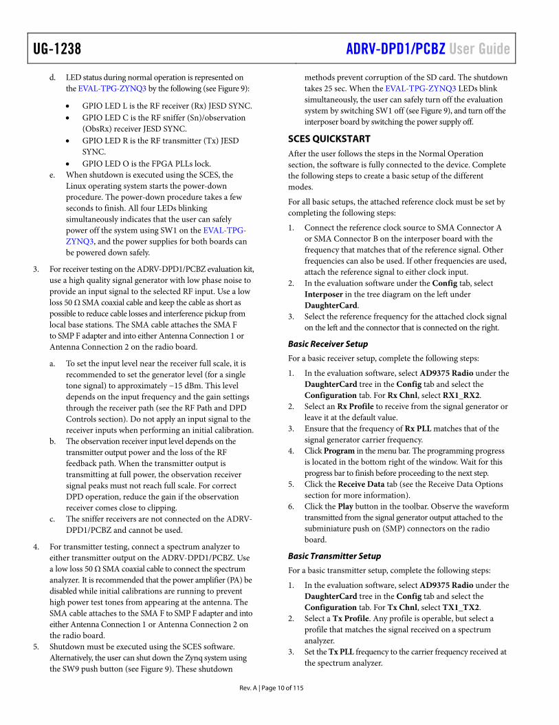
Transmitter Setup ........................................................................... 51 Transmit Data Options .............................................................. 52
RF Path and DPD Controls ........................................................... 53 Transmitter RF Path Controls .................................................. 53 Receiver RF Path Controls ........................................................ 53 DPD Controls ............................................................................. 54
Scripting ........................................................................................... 55 IronPython Script Example ...................................................... 56
Troubleshooting .............................................................................. 58 Startup .......................................................................................... 58
No LED Activity (Zynq) ........................................................ 58 LEDs Active but SCES Reports that Hardware is Not Connected ............................................................................... 58 LED 1 and LED 2 (STATUS 1 and STATUS 0) on Interposer Board Do Not Illuminate After Programming ...................... 58
Error Handling ........................................................................... 58 Typical Performance ...................................................................... 59
Electrical Specifications ............................................................. 60 Bill of Materials ............................................................................... 61 Interposer Board Schematics ........................................................ 68 Radio Board Schematics ................................................................ 88 Interposer Board PCB Layers ..................................................... 102 Radio Board PCB Layers ............................................................. 110 Interposer Board Connectors and LEDs ................................... 114

ADRV-DPD1/PCBZ User Guide UG-1238
Rev. A | Page 3 of 115
REVISION HISTORY 7/2018—Rev. 0 to Rev. A Updated Format.................................................................. Universal Changes to Features Section and General Description Section ....... 1 Changes to Figure 1 Caption ........................................................... 4 Changed Evaluation Board Software Section to Getting Started Section ................................................................................................ 5 Added Software Installation Section .............................................. 5 Changes to SCES Setup Requirements Section and SCES Setup Section ................................................................................................ 5 Changes to Figure 6 Caption ........................................................... 7 Changed Evaluation Board Hardware Section and Hardware Setup Section to Evaluation Kit Setup Section .............................. 7 Changes to Evaluation Kit Setup ..................................................... 7 Changes to Hardware Operation .................................................... 9 Changes to SCES Quickstart Section and Basic Transmitter Setup Section .............................................................................................. 10 Changes to Basic DPD Setup Section ........................................... 11 Added Evaluation Kit Hardware Section, Power Supply Connection Section, and Figure 11; Renumbered Sequentially ............................ 12 Added Figure 12, ADRV-DPD1/PCBZ Top and Bottom View Photographs Section, Figure 13 and Figure 14 ............................ 13 Added Figure 15 to Figure 18, Table 1, and Table 2; Renumbered Sequentially ...................................................................................... 14 Added Interposer Board Reference Section, Figure 19, System Reference Clocks Section, Figure 20, LED Indicators Section, and Figure 21 ........................................................................................... 15 Added Table 3, ADP5054 Enable Jumper Section, Figure 22, EEPROM Write Protect Enable Headers Section, and Figure 23 ........................................................................................... 16 Added Figure 24, Debug Headers Section, RF A Header Pins Section, Figures 25, RF B Header Pins Section, and Figure 26 ..... 17 Added JTAG Header Pins Section, Figure 27, and SPI Chip Select Lines Section .................................................................................... 18 Added Table 4 .................................................................................. 19 Added Pin Configurations and Function Descriptions Section, Figure 28, and Table 5 ..................................................................... 20 Added Figure 29 and Table 6 ......................................................... 23 Added Figure 30, Table 7, and Table 8 .......................................... 27 Added Figure 31, Table 9, and Table 10 ........................................ 28 Added Figure 32 and Table 11 ....................................................... 29
Changed AD9375 Small Cell Reference Design Evaluation Software GUI Operation Section to Using the Software for Testing Section ................................................................................. 30 Added Graphical User Interface Operation Section ................... 30 Changes to Figure 33 Caption ....................................................... 30 Changes to GPIO Tabs Section and Figure 44 Caption ............. 39 Changed Rx, Tx, and ObsRx/Sniffer Summary Tab Section to Rx Summary, Tx Summary, and ObsRx/Sniffer Summary Tabs Section............................................................................................... 40 Changes to Clock Setup Section .................................................... 41 Changed Rx Signal Chain Section to Receive Data Options Section............................................................................................... 48 Changed Observation Rx Signal Chain Section to Observation Receiver Signal Chain Section ....................................................... 49 Changes to Observation Receiver Signal Chain Section ............ 49 Changed Transmitter Data Options Section to Transmit Data Options Section ............................................................................... 52 Changes to Transmit Data Options Section ................................ 52 Changes to DPD Controls Section and Figure 62 Caption ....... 54 Changes to IronPython Script Example Section ......................... 56 Changed LED 1 and LED 2 on Interposer Board Do Not Light up After Programming Section to LED 1 and LED 2 (STATUS 1 and STATUS 0) on Interposer Board Do Not Illuminate After Programming Section ..................................................................... 58 Added Typical Performance Section, Figure 66 to Figure 69, and Table 12 to Table 15 ......................................................................... 59 Added Table 16 to Table 19, Electrical Specifications Section, and Table 20 to Table 21 .................................................................................... 60 Added Bill of Materials Section and Table 22 .............................. 61 Added Table 23 to Table 25 ............................................................ 64 Added Table 26 and Table 27 ......................................................... 67 Added Interposer Board Schematics Section and Figure 70 to Figure 97 ........................................................................................... 68 Added Radio Board Schematics Section and Figure 88 to Figure 116 ......................................................................................... 88 Added Interposer Board PCB Layers Section and Figure 117 to Figure 124 ...................................................................................... 102 Added Radio Board PCB Layers Section Figure 125 to Figure 133 ...................................................................................... 110 1/2018—Revision 0: Initial Version

UG-1238 ADRV-DPD1/PCBZ User Guide
Rev. A | Page 4 of 115
ADRV-DPD1/PCBZ EVALUATION KIT PHOTOGRAPH
1649
3-00
1
Figure 1. ADRV-DPD1/PCBZ Evaluation Kit with Radio Board Heatsink Removed

ADRV-DPD1/PCBZ User Guide UG-1238
Rev. A | Page 5 of 115
GETTING STARTED SOFTWARE INSTALLATION The AD9375 SCES, when connected to the evaluation kit, reads the hardware identification data and verifies that the AD9375 Small Cell Radio Reference Design Evaluation Software GUI is connected to the appropriate hardware. After the evaluation hardware is connected, the desired operating parameters can be set up with SCES, and the software can program the reference platform.
After the device is configured, the evaluation software can transmit waveforms, observe received waveforms, and initiate correction algorithms. In addition, sequences of application programming interface (API) commands in the form of IronPython scripts can be generated and executed using SCES.
SCES SETUP REQUIREMENTS The SCES requires the following:
• An evaluation board for the Xilinx Zynq-7000 system on a chip (SoC) FPGA, such as the EVAL-TPG-ZYNQ3 (not included in the AD9375 evaluation kit). Both the Xilinx EK-Z7-ZC706 Rev 1.2 and Avnet AES-Z7-JESD3-G Rev 1.2 are compatible with the AD9375 evaluation kit.
• The ADRV-DPD1/PCBZ Small Cell Radio Reference design kit.
• Operating system of Windows 7 SP1 or later. • Free Ethernet port or USB to Ethernet adapter. • AD9375 SCES installer, available on the ADRV-DPD1
product page. • Administrative privileges on the controlling PC.
SCES SETUP To install the AD9375 Small Cell Radio Reference Design Evaluation Software GUI, complete the following steps:
1. After the software zip folder downloads, copy the software to the target system and unzip the files. The extracted files include an executable file named Small Cell Evaluation Software Vx.x.x.exe.
2. After running the executable file, a standard installation wizard opens. The wizard, by default, installs optional components, including the Microsoft .NET Framework 4.5 (which is mandatory for the software to operate) and IronPython 2.7.4 (which is optional but recommended), as shown in Figure 3.
3. Open the Start > Run window and type ncpa.cpl into the text box, then click OK (see Figure 2).
1649
3-00
2
Figure 2. Run Window for Network Connections
1649
3-00
3
Figure 3. Software Installation Components

UG-1238 ADRV-DPD1/PCBZ User Guide
Rev. A | Page 6 of 115
4. Enable the selected device, right click on the device, and click Properties.
5. A window appears, as shown in Figure 5. Double click Internet Protocol Version 4 (TCP/IPv4).
6. Select Use the following IP address: and enter the following values:
• IP address: 192.168.1.2. • Subnet mask: 255.255.255.0.
7. Click OK at the bottom of the Internet Protocol Version 4 (TCP/IPv4) Properties window, then click OK at the bottom of the Local Area Connection x Properties window (where x is the number of local area network (LAN) devices installed on the computer). Close the Network Connections window.
8. Create an outbound transmission control protocol (TCP). Create an always allow rule for the firewall for Port 22 and Port 55555 in Windows Firewall or other antivirus programs (such as Avast, Norton, AVG, or Sophos), as shown in Figure 6. Steps for creating these rules in Windows Firewall follow.
9. To create an always allow rule in Windows Firewall, open the Start > Run window and type wf.msc into the box. Click OK (see Figure 4). Approve the User Account Control dialog box by clicking Yes.
1649
3-10
5
Figure 4. Run Window for Windows Firewall
10. In the Windows Firewall with Advanced Security window, click Outbound Rules in the left pane, and click New Rule… in the right pane.
11. Select the following options in the New Outbound Rule Wizard (see Figure 7).
• Under the Rule Type section, select Port, then click Next >.
• Under the Protocol and Ports section, click TCP, click Specific remote ports, and enter 22, 555555. Click Next >.
• Under the Action section, click Allow the connection then click Next >.
• Under the Profile section, select the Domain, Private, and Public check boxes, and click Next >.
• Under the Name section, enter SCES in the Name field, then click Finish.
1649
3-00
4
Figure 5. Internet Protocol (IP) Settings for Ethernet Device

ADRV-DPD1/PCBZ User Guide UG-1238
Rev. A | Page 7 of 115
1649
3-00
5
Figure 6. Windows Firewall with Advanced Security Window
1649
3-10
7
Figure 7. New Outbound Rule Wizard Window

UG-1238 ADRV-DPD1/PCBZ User Guide
Rev. A | Page 8 of 115
EVALUATION KIT SETUP The hardware setup is shown in Figure 8. The Xilinx ZC706 Zynq evaluation board, shown in Figure 8 and Figure 9, is an older model of the EVAL-TPG-ZYNQ3, but the two boards are otherwise identical in terms of connections and compatibility.
To set up the hardware, complete the following steps:
1. Connect the PC and the EVAL-TPG-ZYNQ3 evaluation board with an Ethernet cable.
2. Ensure that all jumpers on the EVAL-TPG-ZYNQ3 are configured as shown in Figure 9, and Switch 1, Switch 2, and Switch 5 are set to the A position and that SW1 is set as shown in Figure 9.
3. Insert the secure digital (SD) card into the EVAL-TPG-ZYNQ3 and connect the interposer board to the connectors on the EVAL-TPG-ZYNQ3, and the radio board to the interposer board using the high pin count (HPC) FPGA mezzanine card (FMC) connectors, as shown in Figure 8. Ensure that the connectors are properly aligned.
4. Ensure that the interposer board Header J16 is set to short the middle two pins, Pin 3 to Pin 4, which is the automatic position (see Figure 133 for the location of these pins).
5. Connect a reference clock signal to the interposer board at J8 (REF_A, default 10 MHz) or J13 (REF_B, default 30.72 MHz). After SCES programs the system, two green light emitting diodes (LEDs) on the interposer board, Status 0 and Status 1, turn on. Lit LEDs indicate that the correct reference clock is provided and the phase locked loops (PLLs) in the AD9528 are locked. The Status 0 LED (PLL1 lock) remains unlit if no reference signal is present. The Status 1 LED (PLL2 lock) is always lit. A suitable input level for the reference signals at J8 or J13 is 380 mVp-p to 1200 mVp-p into 100 Ω (−7 dBm to +3 dBm from a 50 Ω sine wave generator). A square wave is preferred but a sine wave is acceptable. See the System Reference Clocks section for more details
6. Connect the 12 V, 5 A power supply to the EVAL-TPG-ZYNQ3 at the J22 power input.
7. Connect the 12 V, 5 A radio power supply to the interposer board at J14.
12V DCPOWER SUPPLY
ETHERNETCONNECTION
PC RUNNINGEVALUATIONSOFTWARE
12V DCPOWER SUPPLY
SD CARDWITH IMAGE
SIGNAL ANALYZER
SIGNAL SYNTHESIZERANT1
REF B CLOCK SOURCEREF A CLOCK SOURCE
ANT2
1649
3-00
6
Figure 8. Hardware Connection Diagram

ADRV-DPD1/PCBZ User Guide UG-1238
Rev. A | Page 9 of 115
SW9 - SHUTDOWN
J22 - 12V POWER INPUT
J68 – EXTERNAL Rx TRIGGER
J67 – EXTERNAL Tx TRIGGER
GPIO LED L - RF Rx JESD SYNCGPIO LED C – RF Sn/Obs Rx JESD SYNCGPIO LED R – RF Tx JESD SYNCGPIO LED O – FPGA PLLs LOCK
SW1 - POWER SWITCH
SW8 - REBOOT
1649
3-00
7
Figure 9. Xilinx ZC706 Zynq Evaluation Board with Jumper Settings and Switch Position Configured to Work with the ADRV-DPD1/PCBZ
(Identical to the EVAL-TPG-ZYNQ3)
Hardware Operation
To operate the evaluation hardware, complete the following steps:
1. Turn on the evaluation system by switching on both 12 V, 5 A power supplies connected to the EVAL-TPG-ZYNQ3 and the interposer board, then switch the EVAL-TPG-ZYNQ3 power switch, SW1, to the on position.
2. The EVAL-TPG-ZYNQ3 evaluation system uses a Linux operating system. It takes approximately 30 sec before the system is ready for operation and can accept commands from PC software. Boot status can be observed on the EVAL-TPG-ZYNQ3 general-purpose input/output (GPIO) LEDs (L, C, R, and O).
The following is the startup sequence that can be observed when booting the evaluation kit:
a. After turning on SW1, all four LEDs are on for approximately 15 sec. During this time, the Linux boot image is copied from the SD card into the FPGA memory.
b. The LEDs begin flashing (moving the single on light), indicating the Linux operating system is starting up. This startup takes another 15 sec.
c. When the LEDs stop flashing, the system is ready for normal operation and awaits connection with the PC over the Ethernet local area network (LAN), which can be established using the SCES.
UG-1238 ADRV-DPD1/PCBZ User Guide
Rev. A | Page 10 of 115
d. LED status during normal operation is represented on the EVAL-TPG-ZYNQ3 by the following (see Figure 9):
• GPIO LED L is the RF receiver (Rx) JESD SYNC. • GPIO LED C is the RF sniffer (Sn)/observation
(ObsRx) receiver JESD SYNC. • GPIO LED R is the RF transmitter (Tx) JESD
SYNC. • GPIO LED O is the FPGA PLLs lock.
e. When shutdown is executed using the SCES, the Linux operating system starts the power-down procedure. The power-down procedure takes a few seconds to finish. All four LEDs blinking simultaneously indicates that the user can safely power off the system using SW1 on the EVAL-TPG-ZYNQ3, and the power supplies for both boards can be powered down safely.
3. For receiver testing on the ADRV-DPD1/PCBZ evaluation kit, use a high quality signal generator with low phase noise to provide an input signal to the selected RF input. Use a low loss 50 Ω SMA coaxial cable and keep the cable as short as possible to reduce cable losses and interference pickup from local base stations. The SMA cable attaches the SMA F to SMP F adapter and into either Antenna Connection 1 or Antenna Connection 2 on the radio board.
a. To set the input level near the receiver full scale, it is recommended to set the generator level (for a single tone signal) to approximately −15 dBm. This level depends on the input frequency and the gain settings through the receiver path (see the RF Path and DPD Controls section). Do not apply an input signal to the receiver inputs when performing an initial calibration.
b. The observation receiver input level depends on the transmitter output power and the loss of the RF feedback path. When the transmitter output is transmitting at full power, the observation receiver signal peaks must not reach full scale. For correct DPD operation, reduce the gain if the observation receiver comes close to clipping.
c. The sniffer receivers are not connected on the ADRV-DPD1/PCBZ and cannot be used.
4. For transmitter testing, connect a spectrum analyzer to either transmitter output on the ADRV-DPD1/PCBZ. Use a low loss 50 Ω SMA coaxial cable to connect the spectrum analyzer. It is recommended that the power amplifier (PA) be disabled while initial calibrations are running to prevent high power test tones from appearing at the antenna. The SMA cable attaches to the SMA F to SMP F adapter and into either Antenna Connection 1 or Antenna Connection 2 on the radio board.
5. Shutdown must be executed using the SCES software. Alternatively, the user can shut down the Zynq system using the SW9 push button (see Figure 9). These shutdown
methods prevent corruption of the SD card. The shutdown takes 25 sec. When the EVAL-TPG-ZYNQ3 LEDs blink simultaneously, the user can safely turn off the evaluation system by switching SW1 off (see Figure 9), and turn off the interposer board by switching the power supply off.
SCES QUICKSTART After the user follows the steps in the Normal Operation section, the software is fully connected to the device. Complete the following steps to create a basic setup of the different modes.
For all basic setups, the attached reference clock must be set by completing the following steps:
1. Connect the reference clock source to SMA Connector A or SMA Connector B on the interposer board with the frequency that matches that of the reference signal. Other frequencies can also be used. If other frequencies are used, attach the reference signal to either clock input.
2. In the evaluation software under the Config tab, select Interposer in the tree diagram on the left under DaughterCard.
3. Select the reference frequency for the attached clock signal on the left and the connector that is connected on the right.
Basic Receiver Setup
For a basic receiver setup, complete the following steps:
1. In the evaluation software, select AD9375 Radio under the DaughterCard tree in the Config tab and select the Configuration tab. For Rx Chnl, select RX1_RX2.
2. Select an Rx Profile to receive from the signal generator or leave it at the default value.
3. Ensure that the frequency of Rx PLL matches that of the signal generator carrier frequency.
4. Click Program in the menu bar. The programming progress is located in the bottom right of the window. Wait for this progress bar to finish before proceeding to the next step.
5. Click the Receive Data tab (see the Receive Data Options section for more information).
6. Click the Play button in the toolbar. Observe the waveform transmitted from the signal generator output attached to the subminiature push on (SMP) connectors on the radio board.
Basic Transmitter Setup
For a basic transmitter setup, complete the following steps:
1. In the evaluation software, select AD9375 Radio under the DaughterCard tree in the Config tab and select the Configuration tab. For Tx Chnl, select TX1_TX2.
2. Select a Tx Profile. Any profile is operable, but select a profile that matches the signal received on a spectrum analyzer.
3. Set the Tx PLL frequency to the carrier frequency received at the spectrum analyzer.

ADRV-DPD1/PCBZ User Guide UG-1238
Rev. A | Page 11 of 115
4. Click Program in the menu bar. The programming progress can be seen in the bottom right of the window. Wait for the progress bar to finish before proceeding to the next step.
5. Click the Transmit Data tab (see the Transmitter Setup section and Figure 59 for more information).
6. Load waveforms onto Tx1 and Tx2 with the Load Waveform buttons, labeled Load TX1 and Load TX2. There are several waveforms included with the software. Note that the software scales the waveform to full scale 0 dBFS if Scaling required is selected in the Select a file window. Alternatively, tone parameters can be set to generate basic waveforms.
7. Set the Tx RF attenuation and waveform digital attenuation for each Tx channel.
8. Click Run Cals. This process takes a few seconds and the button becomes clickable again once the process is completed.
9. Click Play in the Transmit Data tab toolbar. After a few seconds, the waveform that is sent to the gain amplifier appears.
10. Switch on the gain amplifier in the RF Control tab for the antenna or antennas that have spectrum analyzers connected to them.
11. Switch on the corresponding power amplifiers for the same antennas.
12. When powering down, power down the amplifiers in reverse order. Then the user can then stop or change the waveform in the Transmit Data tab to avoid sending unwanted power to the spectrum analyzer.
Basic DPD Setup
For a basic DPD setup, complete the following steps:
1. After following the steps in the Basic Transmitter Setup section, return to the Config tab and ensure that a TxDPD profile is set in the Tx Profile dropdown menu (see Figure 39).
2. In the Calibration tab, enable all the internal transmitter local oscillator leakage (LOL) and quadrature error correction (QEC) options.
3. Click Program to program the device and wait for the programming to complete.
4. Ensure that all the transmitter LOL and QEC tracking options are enabled on the left of the Transmit Data tab.
5. Click Run Cals. This calibration takes a few seconds; the button becomes clickable when calibration is completed.
6. Click the Play button in the Transmit Data toolbar. After a few seconds, the waveform that is being sent to the gain amplifier appears.
7. Switch on the gain amplifier for the antenna or desired antenna ports.
8. Switch on the corresponding power amplifiers for the antenna ports.
9. Click the DPD Control tab. 10. Select the checkboxes for the desired outputs to enable DPD. 11. Click Start DPD (see Figure 62). Note that the adjacent
channel leakage drops on the spectrum analyzer. 12. When powering down, disable the DPD by clicking Reset
DPD (see Figure 62), and power off the amplifiers in reverse order. The user can then stop or change the waveform in the Transmit Data tab.

UG-1238 ADRV-DPD1/PCBZ User Guide
Rev. A | Page 12 of 115
EVALUATION KIT HARDWARE This section documents both the interposer board (ADRV-INTERPOS1/PCBZ) and the radio board (ADRV-DPD1/PCBZ) reference design. Figure 10 shows the radio board reference design block diagram. The radio board connects to the interposer board, which interfaces the radio board with the EVAL-TPG-ZYNQ3 for controlling it with the SCES.
1649
3-03
6
PA
LNAANT1
ADL5335
AD9375
PA_ENABLE
PA
LNAANT2
ADL5335 PA_ENABLE
Figure 10. AD9375 SCRD Radio Board Receiver and Transmitter RF Paths
POWER SUPPLY CONNECTION There are three power supply connectors on the interposer board: J14, J15, and J26. The power for the interposer board typically comes from J14 with a 2-wire CUI PJ-102BH power supply connector at 12 V. The provided universal ac to dc power adaptor is recommended for powering the interposer board. A laboratory power supply can be used if desired. When using a laboratory power supply, it must supply a nominal dc input voltage of 12 V ±5% and supply 2.0 A for a single radio board or 3.5 A for two simultaneously connected to the interposer board. The DCPP2 series FC6814671 plug (5.5 mm barrel plug to fit a connector with a 2.5 mm center pin) crimped with 16 AWG wire is recommended for use with a laboratory power supply.
The universal ac to dc power adaptor included in this evaluation kit requires an IEC C13 cord to connect to the local ac power outlet. The IEC C13 power cord is not included as part of the evaluation kit.
The J15 and J26 power terminal connectors are labeled as external 5.1 V input, but the connectors are not necessary to power attached radio boards. This voltage is also not recommended to power the radio board using these connectors because the power is provided from the on-board power
distribution when the interposer board is switched on. The J15 and J26 connectors can be used for probing the radio board supply voltages when desired. The other points that can be probed are the not-fitted header Pin J27 and Pin J32. These pins can provide a more accurate reading of the 5.1 V supply, as shown in Figure 72 and Figure 73.
The interposer board is designed with a Schottky diode to protect against accidental connection of reverse polarity dc power and a transient voltage suppressor (TVS) diode to protect against overvoltage.
Take care to avoid applying voltages below −0.3 V or above +14.5 V. Applying voltages below −0.3 V or above +14.5 V can cause one or more of these protective diode clamps to conduct, resulting in large current flow that could blow the fuse. Prolonged application of reverse voltage or overvoltage at high currents can also damage the protection circuitry or blow the on-board fuse.
1649
3-21
1
Figure 11. 12 V DC Barrel Power Connector

ADRV-DPD1/PCBZ User Guide UG-1238
Rev. A | Page 13 of 115
INTERPOSER BOARD
ADP5054QUAD BUCK REGULATOR
12V DC BARRELCONNECTOR
J14
J15
J26
RF CARD A
RF CARD B
5.1VTERMINAL BLOCK
5.1VTERMINAL BLOCK
INTERPOSER BOARDSYSTEMS
EVAL-TPG-ZYNQ3
1649
3-21
2
Figure 12. Power Supply Diagram
ADRV-DPD1/PCBZ TOP AND BOTTOM VIEW PHOTOGRAPHS
1649
3-21
3
Figure 13. ADRV-DPD1/PCBZ Top View with Heatsink Removed
The top side of the ADRV-DPD1/PCBZ interfaces with the heatsink using a thermal gasket. It is possible but not recommended to remove the heatsink by removing three screws on the rear side of the board (as shown in Figure 13).
1649
3-21
4
Figure 14. ADRV-DPD1/PCBZ Bottom View
The bottom side of the PCB directly interfaces with the interposer board via the SAMTEC 100-way 0.8 mm pitch system connector. For more information, see Table 25.

UG-1238 ADRV-DPD1/PCBZ User Guide
Rev. A | Page 14 of 115
83.5
0
88.50
58.30
40.25
29.50
22.7
0
75.5
0
22.7
0
4.30
16.5
0
80.50
44
44
1649
3-21
5
Figure 15. Mechanical Drawing and Dimensions
1649
3-21
6
344.
45
1.60
REF
Figure 16. Thermal Gasket and Heatsink Mechanical Drawing Side View
1649
3-21
7
Figure 17. 3D CAD Drawing of Reference Design
1649
3-21
8
Figure 18. 3D CAD Drawing of Reference Design with Heatsink Removed
Table 1. LTE Band 7 Configuration1
Frequency Band Frequency Range
Duplex Up-Link (MHz) Down-Link (MHz) 7 2500 to 2570 2620 to 2690 FDD 1 Other LTE bands hardware customizations are available upon request.
Table 2. Power Consumption
Parameter Value
Unit Test Conditions Min Typ Max Total Current 2060 2100 mA VDD = 5 V, VDD_IF = 2.5 V, 2T2R, LTE 20 MHz BW, 24 dBm output power (O/P),
DPD enabled Total Power Consumption 10.3 10.5 W VDD = 5 V, VDD_IF = 2.5 V, 2T2R, LTE 20 MHz BW, 24 dBm O/P, DPD enabled Total Power Dissipation 9.8 10 W VDD = 5 V, VDD_IF = 2.5 V, 2T2R, LTE 20 MHz BW, 24 dBm O/P, DPD enabled

ADRV-DPD1/PCBZ User Guide UG-1238
Rev. A | Page 15 of 115
INTERPOSER BOARD REFERENCE
1649
3-21
9
Figure 19. Interposer Board Attached to Radio Board, Heatsink Removed (Top View)
SYSTEM REFERENCE CLOCKS Two system reference clock options are available to provide a reference clock input to the AD9528 JESD204B clock generator. Reference A is the default 10.00 MHz input. Reference B is the default 30.72 MHz input.
It is recommended to use only one input at a time so that the system operates correctly. The selection of the clock source is modified using the SCES (see the Clock Setup section for more details).
CLOCK INPUT REF_B30.72 MHz
CLOCK INPUTREF_A10.00 MHz
AD9528 AUXILIARYCLOCK OUT POSITIVE
AD9528 AUXILIARYCLOCK OUT NEGATIVE
1649
3-22
0
Figure 20. Reference Clock Inputs and Outputs
The input impedance on both clock inputs is 1 MΩ dc and 100 Ω ac.
Clock input signals are ideally in the form of a square wave input in the range of −7 dBm to +3 dBm, although a sine wave input is also acceptable.
In addition, there is an option to fit Resistor R45, Resistor R46, Resistor R52, and Resistor R53 (51 Ω, 0402 size) to the interposer board to give REF_A and REF_B a 50 Ω input impedance.
The system reference clock frequencies mentioned previously are default options. However, the hardware is compatible with reference frequencies from 10 MHz to 80 MHz. Consult the product data sheet for further details on AD9528 PLL operation.
LED INDICATORS There are eight LED indicators in the interposer to show the status of the board.
1649
3-22
1
Figure 21. LED Indicators

UG-1238 ADRV-DPD1/PCBZ User Guide
Rev. A | Page 16 of 115
Table 3. List of LEDs and Associated Functions LED Order1 LED Name Color Function 1 LED 5 Green +12 VDC (VIN_DC) present. 2 LED 8 Green +3.9 VDC (VCC_3V9) present from ADP5054ACPZ-R7 (SW3). 3 LED 9 Green +3.3 VDC (VCC_3V3) present from ADM7154ARDZ-3.3-27. 4 LED 12 Red ADP5054 PWRGD output. Illuminates when ADP5054 Channel 1 (VCC_5V1_A) voltage is not correct. 5 LED 11 Green +5.1 VDC for RF Module B (VCC_5V1_B). Present from ADP5054ACPZ-R7 (SW2) 6 LED 7 Green +5.1 VDC for RF Module A (VCC_5V1_A). Present from ADP5054ACPZ-R7 (SW1). 7 LED 1 Green AD9528 STATUS_1 output. Normally programmed as PLL2 lock indicator. 8 LED 2 Green AD9528 STATUS_0 output. Normally programmed as PLL1 lock indicator. 1 The order of LEDs here is not sequential to how they are listed on the card. See Figure 21 for order of LEDs.
ADP5054 ENABLE JUMPER The ADP5054 enable jumper, labeled J16, is used to select the mode of operation for the ADP5054 power regulator. The modes are as follows:
• Always off: ADP5054 is disabled. • Automatic: ADP5054 is enabled upon detection of PGOOD
signal from EVAL-TPG-ZYNQ3. • Always on: ADP5054 is enabled whenever 12 V is present on
the dc power connector.
For typical operation, place a jumper in the automatic position, shorting Pin 3 and Pin 4. Pin 1 is indicated by a white dot on the board.
1649
3-22
2
Figure 22. ADP5054 Enable Jumper
EEPROM WRITE PROTECT ENABLE HEADERS There are two electronical erasable program memory (EEPROM) write protect enable headers provided on the interposer board, one per RF card. These headers enable or disable write operations to the RF calibration data serial peripheral interface (SPI) EEPROM accessible via the SPI bus and located on the RF card. Note that the SPI EEPROM is currently unsupported in the GUI (SCES), API, and interposer board.
1649
3-22
3
Figure 23. EEPROM Write Protect Header RF A

ADRV-DPD1/PCBZ User Guide UG-1238
Rev. A | Page 17 of 115
1649
3-22
4
Figure 24. EEPROM Write Protect Header RF B
Placement of the jumper ensures that the write protect line is enabled and write operations to the EEPROM are disabled. Removing the header allows write operations to be carried out on the EEPROM over the SPI interface, controlled from the EVAL-TPG-ZYNQ3.
DEBUG HEADERS There are three sets of headers intended as a debug aid to probe signals required for interfacing the RF card and interposer board with the EVAL-TPG-ZYNQ3 platform. The main RF headers have 16-way IDC type connectors that are recommended to be used as protection from shorting pins together accidentally. The 16-way 28 American wire gauge (AWG) ribbon cable can be crimped into these connectors for probing the pins with a logic analyzer or multimeter. A single white dot on the silkscreen indicates Pin 1. Subsequent pins can be then be determined from the schematic in Figure 89.
RF A Header Pins
The RF A headers are located adjacent to where the RF A card fits on the interposer board, as shown in Figure 25. For a complete listing of RF A pin functions and descriptions, see Table 7 and Table 8.
1649
3-22
5
Figure 25. RF A Debug Header Pins
RF B Header Pins
The headers for RF B are located near the interposer board LEDs, as shown in Figure 26. The RF B signals are accessible on the J1 and J9 connectors. For a complete listing of RF B pin functions and descriptions, see Table 9 and Table 10.
1649
3-22
6
Figure 26. RF B Debug Header Pins

UG-1238 ADRV-DPD1/PCBZ User Guide
Rev. A | Page 18 of 115
JTAG Header Pins
The JTAG interface can be probed using the JTAG headers (Figure 27) at J7 with a 2 × 10, 20-way, 0.05 inch pitch rectangular connector that is not included in the evaluation kit. The SAMTEC cable assembly with the FFSD-10-S-12.00-01-N part number is recommended for connecting to these header pins. Note that this JTAG cable connector does not fit if the J2 connector is also attached at the J2 header pins. As such, only the J2 connector or the JTAG interface must be connected at any one time. Take care when connectors are removed from header pins because there is a danger of shorting pins. Insulating tape is recommended to cover the J2 headers when the JTAG headers are in use.
For JTAG boundary scan, refer to the AD9375 System Development User Guide for more information. For a complete list of JTAG pins and descriptions, see Table 11.
1649
3-22
7
Figure 27. JTAG Debug Header Pins
SPI CHIP SELECT LINES The chip select (CS) lines from the EVAL-TPG-ZYNQ3 card via the FMC are encoded and are decoded by the CS decoder circuit on the interposer board shown in Figure 82. The chip select codes for each device are detailed in Table 4 with FMC_SPI_CS0 being the least significant bit (LSB) and FMC_SPI_CS4 the most significant bit (MSB). The codes for each chip select are detailed in Table 4. The Selected Chip Acronym column refers to the name written on the schematics in the interposer board schematics section.
CS0 to CS2 are the device selects, CS3 is the radio board select, and CS4 is for address space expansion. The clock generator on the interposer board appears as an RF A device.

ADRV-DPD1/PCBZ User Guide UG-1238
Rev. A | Page 19 of 115
Table 4. SPI Encoding Codes Chip Select Code Selected Chip Acronym Description 00000 SPI_DRV1_CS_A Chip select driver amplifier on Tx1 on RF Card A, active low. 00001 SPI_DRV2_CS_A Chip select driver amplifier on Tx2 on RF Card A, active low. 00010 SPI_SPARE_CS2 No connect on the ADRV-DPD1/PCBZ. 00011 SPI_EEPROM_CS_A Selects the SPI EEPROM on RF Card A. 00100 SPI_SPARE_CS0 No connect on the ADRV-DPD1/PCBZ. 00101 SPI_PLL_CS Selects the AD9528 phase locked loop generator. 00110 SPI_MYK_CS_A Selects the transceiver device on the RF A Card. 00111, 01111, 1xxxx NC No connect. 01000 SPI_DRV1_CS_B Chip select driver amplifier on Tx1 on RF Card B, active low. 01001 SPI_DRV2_CS_B Chip select driver amplifier on Tx2 on RF Card B, active low. 01010 SPI_SPARE_CS3 No connect on the ADRV-DPD1/PCBZ. 01011 SPI_EEPROM_CS_B Selects the SPI EEPROM on RF Card B. 01100 SPI_SPARE_CS1 No connect on the ADRV-DPD1/PCBZ. 01101 NC No connect. 01110 SPI_MYK_CS_B Selects the transceiver device on the RF B Card.

UG-1238 ADRV-DPD1/PCBZ User Guide
Rev. A | Page 20 of 115
PIN CONFIGURATIONS AND FUNCTION DESCRIPTIONS Not all connections are present on the reference design card that are present on the interposer board. These connections are noted in the pin description.
1
2
99
100 1649
3-22
8
Figure 28. RF Card Pin Configuration
Table 5. RF Card Pin Function Descriptions
RF Pin No. Mnemonic Type1 Description I/O Voltage
1, 2, 7, 8, 13, 14, 19, 20, 25, 26, 32, 38, 44, 49, 50, 56, 61, 66, 75, 76, 85, 89, 90, 91, 92
GND GND Connected to Ground.
3, 5 SYNCINB1−, SYNCINB1+ I Low Voltage Differential Signaling (LVDS) Sync Signal Associated with Observation Receiver/Sniffer Channel Data on the JESD204B Interface.
LVDS
4, 6 SERDOUT3−, SERDOUT3+ O RF Current Mode Logic (CML) Differential Output 3. This JESD204B lane can be used by the receiver data or by the sniffer/observation receiver data.
CML
9, 11 SYNCINB0, SYNCINB0+ I LVDS Sync Signal Associated with Receiver Channel Data on the JESD204B Interface.
LVDS
10, 12 SERDOUT1−, SERDOUT1+ O RF CML Differential Output 1. This JESD204B lane can be used by receiver data or by sniffer/observation receiver data.
CML
15, 17 SYSREF_IN−, SYSREF_IN+ I LVDS System Reference Clock Inputs for the JESD204B Interface. LVDS
16, 18 SERDOUT2−, SERDOUT2+ O RF CML Differential Output 2. This lane can be used by the receiver data or by the sniffer/observation receiver data.
CML
21, 23 DEV_CLK_IN−, DEV_CLK_IN+
I Device Clock LVDS Input, AC-Coupled with a 0.10 μF Capacitor. LVDS
22, 24 SERDOUT0−, SERDOUT0+ O RF CML Differential Output 0. This JESD204B lane can be used by receiver data or by sniffer/observation receiver data.
CML
27 TX2_ENABLE I Enable for Tx2 on the Transceiver Device. On the ADRV-DPD1/PCBZ, this pin is not connected because the TX1_ENABLE pin enables both Tx1 and Tx2 simultaneously.
VDD_IF
28, 30 SERDIN2−, SERDIN2+ I RF CML Differential Input 2. CML
29 RX2_ENABLE I Enable for Rx2 on the Transceiver Device. On the ADRV-DPD1/PCBZ, this pin is not connected because the RX1_ENABLE pin enables both Rx1 and Rx2 simultaneously.
VDD_IF
31 nPRESENCE RF Connected to Ground on Radio Board to Indicate Connection to Interposer Board.
33, 35 TX_DRV1_EN, TX_DRV2_EN
I Enable Line for Tx1 and Tx2 Drivers. This signal is buffered. VDD_IF
34, 36 SERDIN0−, SERDIN0+ I RF CML Differential Input 0. CML
37 RX1_RADIO_EN I Enables the Rx1 and Rx2 Signal Paths on the AD9375. VDD_IF
39, 41 RX_LNA1_EN, RX_LNA2_EN
I Enables the LNA for Rx1 and Rx2 Signal Paths. These lines are buffered. VDD_IF
40, 42 SERDIN3−, SERDIN3+ I RF CML Differential Input 3. CML
43 TX1_RADIO_EN I Enables the Tx1 and Tx2 Signal Paths on the AD9375. VDD_IF
45, 47 TX_PA1_EN, TX_PA2_EN I Enable the SKY66297-11 PA for Tx1 and Tx2 Independently. VDD_IF
46, 48 SERDIN1−, SERDIN1+ I RF CML Differential Input 1. CML
51 GPIO17 I/O General-Purpose Input and Output. This pin is not connected on the ADRV-DPD1/PCBZ.
VDD_IF

ADRV-DPD1/PCBZ User Guide UG-1238
Rev. A | Page 21 of 115
RF Pin No. Mnemonic Type1 Description I/O Voltage
52, 54 SYNCOUTB0−, SYNCOUTB0+
O LVDS Sync Signal Associated with Transmitter Channel Data on the JESD204B Interface.
LVDS
53 EEPROM_WP I Write Protect the SPI EEPROM when Low, Enabled by Jumper on Interposer Board.
GND
55 SPI_EEPROM_CS I Select EEPROM for SPI Communication, Active Low. Pull up this pin to 3.3 V when this pin is floating.
GND
57 SPI_DRV2_CS I Select Tx2 Driver for SPI Communication, Active Low. Pull up this pin to 3.3 V when this pin floating.
GND
58 GPIO11 I/O General-Purpose Input and Output. This pin is not connected on the ADRV-DPD1/PCBZ.
VDD_IF
59 SPI_DRV1_CS I/O Select Tx1 Driver for SPI Communication, Active Low. Pull up this pin to 3.3 V when this pin is floating.
GND
60 GPIO12 I/O General-Purpose Input and Output. This pin is not connected on the ADRV-DPD1/PCBZ.
VDD_IF
62 GPIO13 I/O General-Purpose Input and Output. This pin is not connected on the ADRV-DPD1/PCBZ.
VDD_IF
63 SPI_MYK_CS I Chip Select AD9375 (Mykonos) Device for SPI Communication, Active Low. Pull up this pin to VDD_IF when this pin floating.
GND
64 GPIO14 I/O General-Purpose Input and Output. This pin is not connected on the ADRV-DPD1/PCBZ.
VDD_IF
65 SPI_SCLK I Serial Clock for SPI Communication Referenced to VDD_IF. VDD_IF
67 SPI_MOSI I/O Master Output Slave Input for SPI. This pin is used to write to selected device when device uses 4-wire SPI. Pull up this pin to VDD_IF included.
VDD_IF
68 GPIO15 I/O General-Purpose Input and Output. This pin is not connected on the ADRV-DPD1/PCBZ.
VDD_IF
69 SPI_MISO O Master Input Slave Output for SPI. This pin is used to read from selected device when the device is a 4-wire SPI or as a half-duplex line when the device is a 3-wire SPI. See the SPI Chip Select Lines to understand which chip is selected. Pull up this pin to VDD_IF included.
VDD_IF
70 GPIO8 I/O General-Purpose Input and Output. This pin is not connected on the ADRV-DPD1/PCBZ.
VDD_IF
71 GP_INTERRUPT O General-Purpose AD9375 Interrupt Signal Output. VDD_IF
72 GPIO9 I/O General-Purpose Input and Output. This pin is not connected on the ADRV-DPD1/PCBZ.
VDD_IF
73 RESET I Active Low AD9375 Reset. Pull up this pin to VDD_IF included. VDD_IF
74 GPIO10 I/O General-Purpose Input and Output. No pull-up resistor on ADRV-DPD/PCBZ.
VDD_IF
77 GPIO0 I/O General-Purpose Input and Output. No pull-up resistor on ADRV-DPD/PCBZ.
VDD_IF
78 GPIO4 I/O General-Purpose Input and Output. Pull-up resistor included on ADRV-DPD1/PCBZ.
VDD_IF
79 GPIO1 I/O General-Purpose Input and Output. No pull-up resistor on ADRV-DPD/PCBZ.
VDD_IF
80 GPIO5 I/O General-Purpose Input and Output. Pull-up resistor included on ADRV-DPD1/PCBZ.
VDD_IF
81 GPIO2 I/O General-Purpose Input and Output. No pull-up resistor on ADRV-DPD/PCBZ.
VDD_IF
82 GPIO6 I/O General-Purpose Input and Output. Pull-up resistor included on ADRV-DPD1/PCBZ.
VDD_IF
83 GPIO3 I/O General-Purpose Input and Output. No pull-up resistor on ADRV-DPD/PCBZ.
VDD_IF
84 GPIO7 I/O General-Purpose Input and Output. Pull-up resistor included on ADRV-DPD1/PCBZ.
VDD_IF
86 GPIO18 I/O General-Purpose Input and Output. Pull-up resistor included on ADRV-DPD1/PCBZ.
VDD_IF
87 VDD_IF P CMOS/LVDS Interface Supply to Radio Board. +2.5 V

UG-1238 ADRV-DPD1/PCBZ User Guide
Rev. A | Page 22 of 115
RF Pin No. Mnemonic Type1 Description I/O Voltage
88 TEST I See AD9375 User Guide for JTAG Boundary Scan. VDD_IF
93 to 100 POWER P 5 V Supply Connection to Power the Board. Pin 100 is used as a sense line on the PAs.
+5 V
1 P is power, I is input, O is output, I/O is input/output, and GND is ground.

ADRV-DPD1/PCBZ User Guide UG-1238
Rev. A | Page 23 of 115
The ground connections are not indicated in the pin configuration detailed in Table 6, as all ground connections are marked in the ANSI/VITA 57.1 FPGA mezzanine card (FMC) standard. These connections are also marked in Figure 92, Figure 93, Figure 94, and Figure 95.
The FMC HPC connector pin configuration consists of the following interfaces:
• JESD204B high speed interface between the host (EVAL-TPG-ZYNQ3) and radio transceiver (AD9375). A detailed Analog Devices interface specification is provided in the AD9528 data sheet.
• A subset of the AD9375 GPIOs routed via the interposer.
• PA and LNA control lines for transmit and receive operations.
• SPI interface for AD9375 radio transceiver, as specified in the AD9528 data sheet.
• SPI interface for EEPROM (ON SEMI CAT25128YI-GT3). The AD9375 system development user guide is available as part of the AD9375 design files zip package.
• SPI interface for ADL5335 PGA. • VDD_IF (2.5 V), CMOS, and LVDS signal power. 3P3AUX
(3.3 V) for the interposer board I2C EEPROM, VCC12_P (12 V) is unused on the interposer board.
K40
1649
3-22
9
Figure 29. 400 Pin FMC HPC Connector, Corner Pins Marked
Table 6. FMC HPC Connector Pin Function Descriptions Pin No. EVAL-TPG-ZYNQ3 Mnemonic Interposer Board Mnemonic Description A2, A3 FMC_HPC_DP1_M2C_P,
FMC_HPC_DP1_M2C_N SERDOUT0_A+, SERDOUT0_A−
JESD204B Serial Data From EVAL-TPG-ZYNQ3 to RF Card A.
A6, A7 FMC_HPC_DP2_M2C_P, FMC_HPC_DP2_M2C_N
SERDOUT1_A+, SERDOUT1_A−
JESD204B Serial Data From EVAL-TPG-ZYNQ3 to RF Card A.
A10, A11 FMC_HPC_DP3_M2C_P, FMC_HPC_DP3_M2C_N
SERDOUT3_A+, SERDOUT3_A−
JESD204B Serial Data From EVAL-TPG-ZYNQ3 to RF Card A.
A14, A15 FMC_HPC_DP4_M2C_P, FMC_HPC_DP4_M2C_N
SERDOUT0_B+, SERDOUT0_B−
JESD204B Serial Data From EVAL-TPG-ZYNQ3 to RF Card B.
A18, A19 FMC_HPC_DP5_M2C_P, FMC_HPC_DP5_M2C_N
SERDOUT1_B+, SERDOUT1_B−
JESD204B Serial Data From EVAL-TPG-ZYNQ3 to RF Card B.
A22, A23 FMC_HPC_DP1_C2M_P, FMC_HPC_DP1_C2M_N
SERDIN3_A+, SERDIN3_A−
JESD204B Serial Data From RF Card A to EVAL-TPG-ZYNQ3.
A26, A27 FMC_HPC_DP2_C2M_P, FMC_HPC_DP2_C2M_N
SERDIN0_A+, SERDIN0_A−
JESD204B Serial Data From RF Card A to EVAL-TPG-ZYNQ3.
A30, A31 FMC_HPC_DP3_C2M_P, FMC_HPC_DP3_C2M_N
SERDIN2_A+, SERDIN2_A−
JESD204B Serial Data From RF Card A to EVAL-TPG-ZYNQ3.
A34, A35 FMC_HPC_DP4_C2M_P, FMC_HPC_DP4_C2M_N
SERDIN0_B+, SERDIN0_B−
JESD204B Serial Data From RF Card B to EVAL-TPG-ZYNQ3.
A38, A39 FMC_HPC_DP5_C2M_P, FMC_HPC_DP5_C2M_N
SERDIN1_B+, SERDIN1_B−
JESD204B Serial Data From RF Card B to EVAL-TPG-ZYNQ3.
B1, B4, B5, B8, B9 NC NC No Connect. B12, B13 FMC_HPC_DP7_M2C_P,
FMC_HPC_DP7_M2C_N SERDOUT2_B+, SERDOUT2_B−
JESD204B Serial Data From EVAL-TPG-ZYNQ3 to RF Card B.
B16, B17 FMC_HPC_DP6_M2C_P, FMC_HPC_DP6_M2C_N
SERDOUT3_B+, SERDOUT3_B−
JESD204B Serial Data From EVAL-TPG-ZYNQ3 to RF Card B.
B20, B21 FMC_HPC_GBTCLK1_M2C_P, FMC_HPC_GBTCLK1_M2C_N
FPGA_REF_CLK_A+, FPGA_REF_CLK_A−
Reference Clock A from AD9528 to FPGA.
B24, B25, B28, B29 NC NC No Connect. B32, B33 FMC_HPC_DP7_C2M_P,
FMC_HPC_DP7_C2M_N SERDIN2_B+, SERDIN2_B−
JESD204B Serial Data From RF Card B to EVAL-TPG-ZYNQ3.

UG-1238 ADRV-DPD1/PCBZ User Guide
Rev. A | Page 24 of 115
Pin No. EVAL-TPG-ZYNQ3 Mnemonic Interposer Board Mnemonic Description B36, B37 FMC_HPC_DP6_C2M_P,
FMC_HPC_DP6_C2M_N SERDIN3_B+, SERDIN3_B−
JESD204B Serial Data From RF Card B to EVAL-TPG-ZYNQ3.
B40 NC NC No Connect. C2, C3 FMC_HPC_DP0_C2M_P,
FMC_HPC_DP0_C2M_N SERDIN1_A+, SERDIN1_A−
JESD204B Serial Data From RF Card A to EVAL-TPG-ZYNQ3.
C6, C7 FMC_HPC_DP0_M2C_P, FMC_HPC_DP0_M2C_N
SERDOUT2_A+, SERDOUT2_A−
JESD204B Serial Data From EVAL-TPG-ZYNQ3 to RF Card A.
C10, C11 FMC_HPC_LA06_P, FMC_HPC_LA06_N
FMC_TX1_DRV_EN_A, FMC_TX2_DRV_EN_A
Tx1 and Tx2 Driver Amplifier Enable for RF Card A, Prebuffer.
C14, C15 FMC_HPC_LA10_P, FMC_HPC_LA10_N
FMC_SPI_CS3, FMC_SPI_CS4
SPI Chip Select Multiplex Bits from EVAL-TPG-ZYNQ3 to Interposer Board.
C18, C19 FMC_HPC_LA14_P, FMC_HPC_LA14_N
FMC_TX2_ENABLE_A, FMC_RX2_ENABLE_A
Tx2 and Rx2 Enable on RF Card A Transceiver Device.
C22, C23 FMC_HPC_LA18_CC_P, FMC_HPC_LA18_CC_N
GPIO6_A, GPIO7_A General-Purpose Input and Output.
C26, C27 FMC_HPC_LA27_P, FMC_HPC_LA27_N
FMC_TDD1_SWITCH_A, FMC_TDD2_SWITCH_A
Time Division Duplex 1 and Duplex 2 Switch on RF Card A. No connect on Rev A interposer board 100-pin connector, prebuffer.
C30 FMC_HPC_IIC_SCL FMC_I2C_SCL I2C Interface Clock. C31 FMC_HPC_IIC_SDA FMC_I2C_SDA I2C Interface Data. C34 GA0 EEPROM_A0 I2C EEPROM Address Bit 0. C35, C37 VCC12_P FMCA_VCC_12P0V 12 V from EVAL-TPG-ZYNQ3 Card. C39 VCC3V3 3P3V 3.3 V from EVAL-TPG-ZYNQ3 Card. D1 PWRCTL1_FMC_PG_C2M ADP5054_EN ADP5054 Enabled Signal from Interposer
Board to EVAL-TPG-ZYNQ3. D4, D5 FMC_HPC_GBTCLK0_M2C_P,
FMC_HPC_GBTCLK0_M2C_N FPGA_REF_CLK_B+, FPGA_REF_CLK_B−
Reference Clock B from AD9528 to FPGA.
D8, D9 FMC_HPC_LA01_CC_P, FMC_HPC_LA01_CC_N
SYSREF_FROM_FPGA+, SYSREF_FROM_FPGA−
SYSREF from EVAL-TPG-ZYNQ3 to AD9528 on Interposer Board.
D11 FMC_HPC_LA05_P FMC_TEST JTAG Test Signal from EVAL-TPG-ZYNQ3 to Interposer Board.
D12 FMC_HPC_LA05_N GPIO18_A General-Purpose Input and Output. D14, D15 FMC_HPC_LA09_P,
FMC_HPC_LA09_N FMC_SPI_CS0, FMC_SPI_CS1
SPI Chip Select Multiplex Bits from EVAL-TPG-ZYNQ3 to Interposer Board.
D17, D20, D18, D21
FMC_HPC_LA13_P, FMC_HPC_LA17_CC_P, FMC_HPC_LA13_N, FMC_HPC_LA17_CC_N
FMC_TX1_ENABLE_A, FMC_TX2_ENABLE_B, FMC_RX1_ENABLE_A, FMC_RX2_ENABLE_B
Tx1, Tx2, Rx1, and Rx2 Enable to the Indicated RF Card Transceiver Device.
D23, D24 FMC_HPC_LA23_P, FMC_HPC_LA23_N
FMC_RX1_LNA_ENABLE_A, FMC_RX2_LNA_ENABLE_A
Rx1 and Rx2 Low Noise Amplifier Enable on RF Card A, Postbuffer.
D26 FMC_HPC_LA26_P FMC_CLK_RESET Reset Signal to AD9528, Prebuffer. D27 FMC_HPC_LA26_N FMC_CLK_SYSREF_REQUEST SYSREF Request Signal to AD9528, Prebuffer. D29 FMC_HPC_TCK_BUF NC No Connect on the Interposer Board. D30 FMC_TDI_BUF JTAG_TDI Loopback to the JTAG_TDO Pin. D31 FMC_HPC_TDO_FMC_LPC_TDI JTAG_TDO Loopback to the JTAG_TDI Pin. D32 3P3AUX 3P3VAUX 3.3 V from EVAL-TPG-ZYNQ3 Card. D33 FMC_HPC_TMS_BUF NC No Connect on Interposer Board. D34 NC NC No Connect. D35 GA1 EEPROM_A1 I2C EEPROM Address Bit 1. D36, D38, D40 VCC3V3 3P3V 3.3 V from EVAL-TPG-ZYNQ3 Card. E2, E3 NC NC No Connect. E3 NC NC No Connect. E6, E7, E9, E10,
E12, E13 NC GPIO10_A, GPIO11_A,
GPIO16_A, GPIO17_A, GPIO13_B, GPIO14_B
General-Purpose Input and Output. These pins are not connected on the EVAL-TPG-ZYNQ3.

ADRV-DPD1/PCBZ User Guide UG-1238
Rev. A | Page 25 of 115
Pin No. EVAL-TPG-ZYNQ3 Mnemonic Interposer Board Mnemonic Description E15, E16, E18, E19,
E21, E22, E24, E25, E27, E28, E30, E31, E33, E34, E36, E37
NC NC No Connect.
E39, F40, G39, H40 VADJ FMC_VDD_IF LVDS Supply on EVAL-TPG-ZYNQ3 and CMOS Digital Power Supply for the Radio Board and Interposer Board.
F1 FMC_HPC_PG_M2C 3P3V 3.3 V from EVAL-TPG-ZYNQ3 Card. F4, F5 NC NC No Connect. F7, F8, F10, F11,
F13, F14, F16, F17
NC GPIO8_A, GPIO9_A, GPIO14_A, GPIO15_A, GPIO11_B, GPIO12_B, GPIO16_B, GPIO17_B
General-Purpose Input and Output. No connect on the EVAL-TPG-ZYNQ3.
F19, F20, F22, F23, F25, F26, F28, F29, F31, F32, F34, F35, F37, F38
NC NC No Connect.
G2, G3 FMC_HPC_CLK1_M2C_P, FMC_HPC_CLK1_M2C_N
NC No Connect on Interposer Board.
G6, G7 FMC_HPC_LA00_CC_P, FMC_HPC_LA00_CC_N
FPGA_SYSREF+, FPGA_SYSREF−
SYSREF from Interposer Board to EVAL-TPG-ZYNQ3.
G9, G10 FMC_HPC_LA03_P, FMC_HPC_LA03_N
SYNCINB0_A+, SYNCINB0_A−
JESD204B SYNCIN Signal to RF Card A.
G12 FMC_HPC_LA08_P FMC_SPI_MISO SPI Data from EVAL-TPG-ZYNQ3 to Chip Selected. Also half duplex line for some devices, prebuffer.
G13 FMC_HPC_LA08_N FMC_SPI_CS2 SPI Chip Select Multiplex Bits from EVAL-TPG-ZYNQ3 to Interposer Board.
G15, G16 FMC_HPC_LA12_P, FMC_HPC_LA12_N
FMC_TX1_ENABLE_B, FMC_RX1_ENABLE_B
Tx1 and Rx1 Enable on RF Card B Transceiver Device, Prebuffer.
G18, G19, G21, G22, G24, G25
FMC_HPC_LA16_P, FMC_HPC_LA16_N, FMC_HPC_LA20_P, FMC_HPC_LA20_N, FMC_HPC_LA22_P, FMC_HPC_LA22_N
GPIO2_A, GPIO3_A, GPIO4_B, GPIO5_B, GPIO0_B, GPIO1_B
General-Purpose Input and Output.
G27, G28 FMC_HPC_LA25_P, FMC_HPC_LA25_N
SYNCINB1_A+, SYNCINB1_A−
JESD204B SYNCIN signal to RF Card A.
G30, G31 FMC_HPC_LA29_P, FMC_HPC_LA29_N
GPIO6_B, GPIO7_B General-Purpose Input and Output.
G33, G34 FMC_HPC_LA31_P, FMC_HPC_LA31_N
SYNCINB1_B+, SYNCINB1_B−
JESD204B SYNCIN Signal to RF Card B.
G36, G37 FMC_HPC_LA33_P, FMC_HPC_LA33_N
FMC_TX1_PA_ENABLE_B, FMC_TX2_PA_ENABLE_B
Tx1 and Tx2 Power Amplifier Enable on RF Card B, Prebuffer.
H1 NC NC No Connect. H2 FMC_HPC_PRSNT_M2C_B FMC_RF_PRESENCE Active Low Presence Signal from Radio
Board. H4, H5 FMC_HPC_CLK0_M2C_P,
FMC_HPC_CLK0_M2C_N NC No Connect on Interposer Board.
H7, H8 FMC_HPC_LA02_P, FMC_HPC_LA02_N
SYNCOUTB0_A+, SYNCOUTB0_A−
JESD204B SYNCOUT Signal to RF Card A.
H10 FMC_HPC_LA04_P FMC_RESET_A Reset Signal to Transceiver Device on RF Card A, Prebuffer.
H11 FMC_HPC_LA04_N FMC_GP_INTERRUPT_A General-Purpose Interrupt from the Transceiver Device on RF card A, Postbuffer.
H13 FMC_HPC_LA07_P FMC_SPI_CLK SPI Clock Signal from EVAL-TPG-ZYNQ3 to Selected Chip.
H14 FMC_HPC_LA07_N FMC_SPI_MOSI SPI Data from Chip Selected to EVAL-TPG-ZYNQ3, Prebuffer.

UG-1238 ADRV-DPD1/PCBZ User Guide
Rev. A | Page 26 of 115
Pin No. EVAL-TPG-ZYNQ3 Mnemonic Interposer Board Mnemonic Description H16, H17 FMC_HPC_LA11_P,
FMC_HPC_LA11_N SYNCOUTB0_B+, SYNCOUTB0_B−
JESD204B SYNCOUT Signal to RF Card B.
H19, H20, H22, H23, H25, H26
FMC_HPC_LA15_P, FMC_HPC_LA15_N, FMC_HPC_LA19_P, FMC_HPC_LA19_N, FMC_HPC_LA21_P, FMC_HPC_LA21_N
GPIO0_A, GPIO1_A, GPIO2_A, GPIO3_A, GPIO4_A, GPIO5_A
General-Purpose Input and Output.
H28, H29 FMC_HPC_LA24_P, FMC_HPC_LA24_N
FMC_TX1_PA_ENABLE_A, FMC_TX2_PA_ENABLE_A
Tx1 and Tx2 Power Amplifier Enable on RF Card A, Prebuffer.
H31, H32 FMC_HPC_LA28_P, FMC_HPC_LA28_N
FMC_RX1_LNA_ENABLE_B, FMC_RX2_LNA_ENABLE_B
Rx1 and Rx2 Low Noise Amplifier Enable on RF Card B, Postbuffer.
H34, H35 FMC_HPC_LA30_P, FMC_HPC_LA30_N
SYNCINB0_B+, SYNCINB0_B−
JESD204B SYNCIN Signal to RF Card B.
H37, H38 FMC_HPC_LA32_P, FMC_HPC_LA32_N
FMC_TX1_DRV_EN_B, FMC_TX2_DRV_EN_B
Tx1 and Tx2 Driver Amplifier Enable for RF Card B, Prebuffer.
J2, J3 NC NC No Connect. J6, J7 NC FMC_TDD1_SWITCH_B,
FMC_TDD2_SWITCH_B Time Division Duplex 1 and Duplex 2 Switch on RF Card B. Not connected on Rev. A interposer board 100-pin connector, prebuffer.
J9, J10, J12, J13, J15
NC GPIO12_A, GPIO13_A, GPIO9_B, GPIO10_B, GPIO18_B
General-Purpose Input and Output. Not connected on the EVAL-TPG-ZYNQ3.
J16, J18, J19, J21, J22, J24, J25, J27, J28, J30, J31, J33, J34, J36, J37, J39, K1, K4, K5
NC NC No Connect.
K7, K8 NC FMC_RF_PRESENCE_A, FMC_RF_PRESENCE_B
Presence Signal from RF Card Indicated, Active Low.
K10 NC FMC_RESET_B Reset Signal to Transceiver Device on RF Card B, Prebuffer.
K11 NC FMC_GP_INTERRUPT_B General-Purpose Interrupt from the Transceiver Device on RF Card B, Postbuffer. Not connected on EVAL-TPG-ZYNQ3.
K13, K14 NC GPIO8_B, GPIO15_B General-Purpose Input and Output. Not connected on the EVAL-TPG-ZYNQ3.
K16, K17, K19, K20, K22, K23, K25, K26, K28, K29, K31, K32, K34, K35, K37, K38, K40
NC NC No Connect.

ADRV-DPD1/PCBZ User Guide UG-1238
Rev. A | Page 27 of 115
SPI_DRV1_CS_ASPI_DRV2_CS_ASPI_MOSI
1 23 45 67 89 10
11 1213 1415 16
J2
SPI_MISOSPI_CLK
TX1_PA_ENABLE_ATX2_PA_ENABLE_ATDD1_SWITCH_A
TX2_ENABLE_ATX1_ENABLE_A
RX1_LNA_ENABLE_ARX2_LNA_ENABLE_A
1 23 45 67 89 10
11 1213 1415 16
J10
TEST_A
GPIO3_A
GPIO0_AGPIO1_AGPIO2_A
FMC_SPI_CLKFMC_SPI_MISOFMC_SPI_MOSI
TX1_DRV_EN_ATX2_DRV_EN_A
VDD_IF
FMC_RESET_A
RX2_ENABLE_ARX1_ENABLE_A
VDD_IF
ISENSE_5V1_A NC
TDD2_SWITCH_A
1649
3-23
0
Figure 30. RF A J10 and J2 Debug Headers Pin Configuration
Table 7. J10 Debug Headers Pin Function Descriptions Pin No. Mnemonic Description 1 VDD_IF CMOS and LVDS Supply, 2.5 V Nominal. 2, 4 SPI_DRV1_CS_A,
SPI_DRV2_CS_A Low Indicates Tx1 and Tx2 Driver is Selected for SPI Communication on RF Card A.
3, 5 TX1_DRV_EN_A, TX2_DRV_EN_A
Tx1 and Tx2 Driver on RF Card A Enabled when High.
6 SPI_MOSI SPI Master Out Slave In Signal from EVAL-TPG-ZYNQ3 Postbuffer. 7 FMC_SPI_CLK SPI Clock Signal from EVAL-TPG-ZYNQ3 Prebuffer. 8 SPI_MISO SPI Master In Slave Out Signal from Device Selected for SPI Communication Prebuffer. 9 FMC_SPI_MISO SPI Master In Slave Out Signal from Device Selected for SPI communication Postbuffer. 10 SPI_CLK SPI Clock Signal from EVAL-TPG-ZYNQ3 Postbuffer. 11 FMC_SPI_MOSI SPI Master Out Slave In Signal from EVAL-TPG-ZYNQ3 Prebuffer. 12 FMC_RESET_A Transceiver Device Reset Signal Active Low for RF Board A Prebuffer. 13 NC No Connect. 14 TEST_A Used for JTAG Boundary Scan. If the JTAG boundary scan is desired, an 0402 size 0 Ω resistor must be
soldered to the solder pads labeled R129. TEST_A then yields a buffered output of FMC_TEST. Otherwise, this pin can be left floating.
15 ISENSE_5V1_A Output of AD8211 Current Shunt Monitor for RF Card A. 16 GND Connected to Ground.
Table 8. J2 Debug Headers Pin Function Descriptions Pin No. Mnemonic Description 1 VDD_IF CMOS and LVDS Supply, 2.5 V Nominal. 2, 4 TX1_ENABLE_A, TX2_ENABLE_A Enable Signal to the Transceiver Device on RF Card A for Tx1 and Tx2. 3, 5 RX1_ENABLE_A, RX2_ENABLE_A Enable Signal to the Transceiver Device on RF Card A for Rx1 and Rx2. 6, 8 RX1_LNA_ENABLE_A, RX2_LNA_ENABLE_A Enable Signal to the LNA on RF Card A for Rx1 and Rx2. 7, 9, 11, 13 GPIO0_A, GPIO1_A, GPIO2_A, GPIO3_A General-Purpose Input and Output Monitoring for RF Card A. 10, 12 TX1_PA_ENABLE_A, TX2_PA_ENABLE_A Enable Signal to the PA on RF Card A for Tx1 and Tx2. 14, 15 TDD1_SWITCH_A, TDD2_SWITCH_A Time Division Duplex Switch to RF Card A. Not connected on ADRV-DPD1 RF card. 16 GND Connected to Ground.

UG-1238 ADRV-DPD1/PCBZ User Guide
Rev. A | Page 28 of 115
SPI_DRV1_CS_B
SPI_DRV2_CS_B
1 2
3 4
5 6
7 8
9 10
11 12
13 14
15 16
J1
1 2
3 4
5 6
7 8
9 10
11 12
13 14
15 16
J9
GPIO3_B
GPIO0_B
GPIO1_B
GPIO2_BTX1_PA_ENABLE_B
TX2_PA_ENABLE_B
TDD1_SWITCH_B
TX2_ENABLE_B
TX1_ENABLE_B
RX1_LNA_ENABLE_B
RX2_LNA_ENABLE_B
FMC_SPI_CS4
FMC_SPI_CS1
FMC_SPI_CS2
FMC_SPI_CS0
FMC_SPI_CS3
TX2_DRV_EN_B
FMC_RESET_B
RX2_ENABLE_B
RX1_ENABLE_B
VDD_IF
TEST_B
FMC_I2C_SDA
FMC_I2C_SCL
ISENSE_5V1_B
TX1_DRV_EN_B
VDD_IF
TDD2_SWITCH_B
1649
3-23
1
Figure 31. RF B J1 and J9 Debug Headers Pin Configuration
Table 9. J1 Debug Header Pin Function Descriptions Pin No. Mnemonic Description 1 VDD_IF CMOS and LVDS Supply, 2.5 V Nominal. 2, 3 TX1_DRV_EN_B, TX2_DRV_EN_B Tx1 and Tx2 Driver on RF Card B Enabled when High. 4, 6 SPI_DRV1_CS_B, SPI_DRV2_CS_B Low Indicates Tx1 and Tx2 Driver is Selected for SPI Communication on RF Card B. 5, 7, 9,
11, 13 FMC_SPI_CS0, FMC_SPI_CS1, FMC_SPI_CS2, FMC_SPI_CS3, FMC_SPI_CS4
Serial Peripheral Interface Encoded Bit, see SPI Chip Select Lines for Code Table.
8, 10 FMC_I2C_SDA, FMC_I2C_SCL I2C Serial Data and Clock Line from EVAL-TPG-ZYNQ3. 12 FMC_RESET_B Transceiver Device Reset Signal Active Low for RF Card B Prebuffer. 14 TEST_B Used for JTAG Boundary Scan. To perform a JTAG boundary scan, an 0402 size 0 Ω
resistor must be soldered to solder pads labeled R89. This pin is then a buffered output of FMC_TEST. Otherwise, this pin can be left floating.
15 ISENSE_5V1_B Output of AD8211 Current Shunt Monitor for RF Card B. 16 GND Connected to Ground.
Table 10. J9 Debug Header Pin Function Descriptions Pin No. Mnemonic Description 1 VDD_IF CMOS and LVDS Supply, 2.5 V Nominal. 2, 4 TX1_ENABLE_B, TX2_ENABLE_B Enable Signal to the Transceiver Device on RF Card B for Tx1 and Tx2. 3, 5 RX1_ENABLE_B, RX2_ENABLE_B Enable Signal to the Transceiver Device on RF Card B for Rx1 and Rx2. 6, 8 RX1_LNA_ENABLE_B, RX2_LNA_ENABLE_B Enable Signal to the LNA on RF Card B for Rx1 and Rx2. 7, 9, 11, 13 GPIO0_B, GPIO1_B, GPIO2_B, GPIO3_B General-Purpose Input and Output Monitoring for RF Card B. 10, 12 TX1_PA_ENABLE_B, TX2_PA_ENABLE_B Enable Signal to the PA on RF Card B for Tx1 and Tx2. 14, 15 TDD1_SWITCH_B, TDD1_SWITCH_B Time Division Duplex Switch to RF Card B. Not connected on ADRV-DPD1 RF card. 16 GND Connected to Ground.

ADRV-DPD1/PCBZ User Guide UG-1238
Rev. A | Page 29 of 115
1 23 45 67 89 10
11 1213 14
161820
151719
J7
VDD_IF
TMSTCLKTDOTDI
R12751kΩ
GPIO7_AGPIO18_AGPIO5_AGPIO6_A
GPIO4_A
JTAG
TRST
1649
3-23
2
Figure 32. JTAG Pin Configuration
Table 11. JTAG Debug Header Pin Function Descriptions Pin No. Mnemonic Type1 Description 1 VDD_IF O CMOS and LVDS supply, 2.5 V nominal. 2 TMS O JTAG test mode select line, connected to GPIO 7 on RF card A. 3, 5, 9, 15, 17, 19 GND GND Connected to ground. 4 TCLK O JTAG test clock line, connected to GPIO 18 on RF card A. 6 TDO O JTAG test data out line, connected to GPIO 5 on RF card A. 7, 10 to 14, 18, 20 NC NC Not connected, this pin can be left floating. 8 TDI O JTAG test data in line, connected to GPIO 6 on RF card A. 16 TRST O JTAG test reset active low. 1 O is the output from the header pins. GND is ground. NC is no connect.

UG-1238 ADRV-DPD1/PCBZ User Guide
Rev. A | Page 30 of 115
USING THE SOFTWARE FOR TESTINGGRAPHICAL USER INTERFACE OPERATION The GUI is the controller of the ADRV-DPD1/PCBZ and interposer board. It controls the connection to the EVAL-TPG-ZYNQ3 and interfaces with the ADRV-DPD1/PCBZ through the EVAL-TPG-ZYNQ3.
1. Connect to the EVAL-TPG-ZYNQ3 by clicking Connect from the graphical user interface (GUI) menu. Once connected, the hardware tree pane on the left side of the window updates with the radio board and the interposer board, shown in Figure 37.
2. When connecting to the EVAL-TPG-ZYNQ3 for the first time, the user must update the device platform files by clicking Device > Update > Platform Files.
3. Select the interposer board from the hardware tree pane, and from the Ref Clock Setup tab (see Figure 46), select the desired reference clock.
4. Select the radio board from the hardware tree view and from the Config tab, select the desired radio configuration.
5. Use the other configuration tab (see the Configuring the AD9375 section) for the radio board to set up the desired configuration.
6. When all the configuration tabs are completed as desired, click Program in the menu bar to configure the ADRV-DPD1/PCBZ and ADRV-INTERPOS1/PCBZ evaluation kit.
7. The AD9375 is in radio on mode. 8. In transmit mode, the user can load data to send via the
Transmit Data tab from the system tabs. Test waveform data can be loaded from a file, or the built-in tone generator tool (see Figure 60) can be used to generate data. Click Play to send the waveform data to the transmit.
9. Use the RF Controls tab from the system tabs to configure the transmit RF path from the AD9375 to the antenna connectors.
10. In receive mode, the Receive Data tab can observe data received by the AD9375. Use the RF Controls tab from the system tabs to enable or disable the low noise amplifiers
(LNAs) in the receive RF path from the antenna connectors to the AD9375.
11. Use the DPD Control tab from the system tabs to enable or disable DPD adaptation on the transmit paths.
STARTING THE AD9375 SCES Start the GUI by clicking Start > All Programs > Analog Devices > Small Cell Evaluation Software > Small Cell Evaluation Software. Figure 34 shows the opening page of the SCES after it is activated.
Demo Mode
Figure 35 shows the opening page of the SCES when the evaluation hardware is not connected. The user can use the software in demo mode by completing the following steps:
1. Click Connect in the top left corner of the window. 2. Click OK in the Zynq Not connected error box (see Figure 33).
1649
3-11
0
Figure 33. Zynq Not connected Window
3. After clicking OK, the software progresses into demo mode, in which a superset of all features is displayed.
Connection status is indicated at the bottom of the software window titled Zynq Platform. When the status display reads Disconnected, the SCES is operating in demo mode.
Demo mode is a generic limited version of the software that provides an overview of the transceiver features and evaluation software. Demo mode does not support some features that are specific to the ADRV-DPD1/PCBZ.

ADRV-DPD1/PCBZ User Guide UG-1238
Rev. A | Page 31 of 115
1649
3-00
9
Figure 34. ADRV-DPD1/PCBZ SCES Opening Page
1649
3-01
0
Figure 35. SCES Demo Mode

UG-1238 ADRV-DPD1/PCBZ User Guide
Rev. A | Page 32 of 115
NORMAL OPERATION When the hardware is connected to a PC and the user wants to use the complete evaluation system, SCES establishes a connection to the Zynq system via the Ethernet cable after the user clicks Connect. When a proper connection is established, the software identifies the hardware connected. The software exits demo mode and enters small cell evaluation system connected mode. The daughter card device tree updates and shows the connected radio board and interposer board.
The user can click the DaughterCard option in the device tree, shown in Figure 37. After selecting DaughterCard, information about revisions of different setup blocks appears in the main window. The bottom of that window shows the TCP IP address, set to 192.168.1.10, and the port number, set to 55555. Figure 36 shows an example of the correct connection between a PC and a Zynq system with a daughter card connected to it.
1649
3-01
2
Figure 36. Correct PC Zynq Connection with Daughter Card
Software Update
Typically, when installing an SCES update, the user is also required to update the platform files. The user can perform a platform files update by clicking Device > Update > Platform Files. SCES automatically updates files on the EVAL-TPG-ZYNQ3 SD card and reboots the ADRV-DPD1/PCBZ system.
When all updates are installed, the system is ready for normal operation.
Full version details of the software and hardware can be retrieved by clicking Help > About in the SCES menu.
1649
3-01
1
Figure 37. Project Setup Page of the ADRV-DPD1/PCBZ Software

ADRV-DPD1/PCBZ User Guide UG-1238
Rev. A | Page 33 of 115
1649
3-01
3
Figure 38. Checking the Full Version Details of the Hardware and Software
GUI REFERENCE The following sections outline all the options within the pages and tabs of the SCES for user reference.
Configuring the AD9375
The SCES contains four main user configurable tabs (see Figure 39, Figure 40, Figure 41, and Figure 46). After the user selects AD9375 Radio Card in the device tree, the Config tab appears. Contained within this tab are nine subtabs that contain setup options for the device.
Configuration Tab
The first tab displayed is the Configuration tab. When this tab is selected, the initial screen appears, shown in Figure 39, and the user can select the following:
• The device clock frequency • The number of active receive channels • The number of active transmit channels • The observation/sniffer input • Profiles for receiver, transmitter, observation receiver, and
sniffer receiver • Receiver, transmitter, and sniffer receiver/observation
receiver local oscillator (LO) frequency
The small cell reference design (SCRD) radio has frequency-selective components in the RF paths. The LO frequencies chosen and the RF signal bandwidths used to contain the RF signal entirely within the specified operating bandwidth. For third generation partnership project long-term evolution (3GPP LTE) Band 7 radio boards, the usable transmitter range for a 20 MHz signal bandwidth is 2630 MHz to 2680 MHz, as the Band 7 specification is 2620 MHz to 2690 MHz.

UG-1238 ADRV-DPD1/PCBZ User Guide
Rev. A | Page 34 of 115
1649
3-01
4
Figure 39. Configuration Tab

ADRV-DPD1/PCBZ User Guide UG-1238
Rev. A | Page 35 of 115
Calibration Tab
The second user configurable tab is Calibration, and it enables initializations and tracking receiver/transmitter QEC and LOL calibrations. Figure 40 shows a configuration example. The user can enable or disable initialization calibrations as well as tracking calibrations.
For External Tx LOL initialization calibration together with either Tx1 LOL or Tx2 LOL tracking calibrations, use an external circuit. This section explains the internal hardware configuration only. Refer to the AD9375 Design File Package for details on the external hardware configuration. The External Init Attn option allows the user to control the level of attenuation applied initially at both of the AD9375 transmitter outputs simultaneously.
1649
3-01
5
Figure 40. Calibration Tab

UG-1238 ADRV-DPD1/PCBZ User Guide
Rev. A | Page 36 of 115
JESD204b Setup Tab
The third user configurable tab is JESD204b Setup, which sets the characteristics of the digital data interface. Figure 41 shows a configuration example. The user can set the desired JESD204B lane configuration, select scrambling, and determine whether the selected framer/deframer relinks on SYSREF.
The user can also select the use of an internal (free running) or external (provided by the AD9528) SYSREF to synchronize the JESD204B links.
Note that the receiver and observation receiver share JESD204B lanes. Lanes configured for receiver cannot also be used for the observation receiver.
1649
3-01
6
Figure 41. JESD204b Setup Tab

ADRV-DPD1/PCBZ User Guide UG-1238
Rev. A | Page 37 of 115
AGC Tab
The automatic gain control (AGC) can be configured in the AGC tab. For details about modifiable settings for the AGC and
consequent changes on the AD9375 device, refer to the AD9375 Design File Package.
1649
3-1 1
9
Figure 42. AGC Tab

UG-1238 ADRV-DPD1/PCBZ User Guide
Rev. A | Page 38 of 115
GPIO Tabs
The GPIO Config tab and the 3v3 GPIO tab are used for GPIO configuration.
The GPIO Config tab contains all the configuration options for the GPIO header pins on the interposer board that the user can configure to debug, test, or evaluate the SCRD.
The pins are for interfacing with test equipment or providing signals to output devices such as LEDs, or inputting options with switches.
The function of each pin is defined in this tab. The state of the pins written or read by the SCRD can be verified with the software by clicking Check GPIO. After changing options in the tab, clicking Program GPIO updates the configuration in the hardware.
GPIO Pin 8, Pin 9, and Pin 11 to Pin 17 are not connected to the radio board, but can still be controlled in the GPIO Config tab.
1649
3-01
7
Figure 43. GPIO Config Tab

ADRV-DPD1/PCBZ User Guide UG-1238
Rev. A | Page 39 of 115
The 3v3 GPIO tab sets the characteristics of the 3.3 V GPIO interface of the AD9375.
For the ADRV-DPD1/PCBZ, the AD9375 3v3 GPIO Pin 0 to Pin 5 are used for devices on board. It is not recommended to use these pins, because using these pins may yield unexpected results,
and the settings are overwritten by the software when required. Connections for these pins are shown in Figure 102.
3v3 GPIO Pin 6 to Pin 11 are not connected to anything on the radio board, but can still be controlled in the 3v3 GPIO tab.
Figure 44 shows the default configuration.
1649
3-01
8
Figure 44. 3v3 GPIO Tab

UG-1238 ADRV-DPD1/PCBZ User Guide
Rev. A | Page 40 of 115
Rx Summary, Tx Summary, and ObsRx/Sniffer Summary Tabs
The Rx Summary, Tx Summary, and ObsRx/Sniffer Summary tabs summarize the setup and include a corresponding graph. They are based on the profile selection in the Configuration tab (see Figure 39). In each of these tabs, the user can check clock rates at each filter node, as well as filter characteristics and their pass band flatness.
Quick zooming capability allows zooming of the pass band response by using the mouse cursor to drag a box to select the
zoom area, as well as restoring the plot to full scale by right clicking on the graph area and selecting Zoom Out.
The SCES also provides the capability to export the data plotted on the graphs to an external file. This export is performed by right clicking on the graph area and selecting Export Data to File. Data can then be saved to a file for later analysis.
Figure 45 shows an example of the Rx Summary tab with the resulting composite filter response for the chosen profile.
1649
3-01
9
Figure 45. Rx Summary Tab

ADRV-DPD1/PCBZ User Guide UG-1238
Rev. A | Page 41 of 115
Clock Setup
The interposer board utilizes the AD9528 clock device to provide the main clock (DEV_CLK) and SYSREF with pulses to the AD9375 via the 100-way connector. The interposer board also provides various clocks and SYSREF with pulses to the FPGA on the EVAL-TPG-ZYNQ3 via the FMC connector.
The AD9528 can be configured using the Ref Clock Setup tab, as shown in Figure 46.
Set the values of the reference clock inputs for Ref A and Ref B using the respective boxes, and select the active reference clock using Ref Clock Selection.
For details on the connections on the interposer board, refer to the System Reference Clocks section.
1649
3-02
0
Figure 46. Ref Clock Setup Tab

UG-1238 ADRV-DPD1/PCBZ User Guide
Rev. A | Page 42 of 115
1649
3-02
1
Figure 47. Device Programmed Successfully
Programming the Evaluation System After all the tabs are configured, the user can click Program. The SCES sends a series of API commands that are executed by a dedicated Linux application running on the EVAL-TPG-ZYNQ3. When programming is complete, the system is ready to operate. A progress bar is visible at the bottom of the window. Figure 47 shows the window with the progress bar and message after the device has been programmed.
OTHER SCES FEATURES The AD9375 SCES software provides the user with multiple options to store and load SCES configurations as well as hardware configurations.
Device Dropdown Menu
Figure 48 shows all commands in the Device dropdown menu. The Device dropdown menu allows the user to select the following commands:
• Click Update > Platform Files when a new version of the AD9375 SCES software is installed or prior to first time use, when files stored on the EVAL-TPG-ZYNQ3 SD card need to be updated. See the Software Update section for more details.
• Click Reboot Zynq Platform when a soft restart of the evaluation system is desired.
• Click Shutdown Zynq Platform when the user wants to power down the ADRV-DPD1/PCBZ. The user must use this command to execute the correct power-down sequence. If this procedure is not followed, the file system on the SD card can become corrupted and cause the ADRV-DPD1/PCBZ system to stop operating.
File Dropdown Menu Figure 49 shows all commands in the File dropdown menu. The File dropdown menu allows the user to select the following commands:
• Save GUI Setup stores all AD9375 SCES configuration settings. SCES generates an XML file with all software settings recorded. The user can reload software settings by clicking Load Setup and selecting the saved setup file.
• Load GUI Setup loads all AD9375 SCES configuration settings stored in XML files that were saved using the Save GUI Setup command.
• Load Custom Profile loads a custom version of the AD9375 SCES profile. Use separate software to generate an AD9375 custom profile.
• Clear Custom Profile restores the AD9375 SCES software to its state prior to loading custom profile using the Load Custom Profile command.
• View Log Files monitors API activities. This command opens the window shown in Figure 50. In this window, the user can select from the following options: • AD9371DLL Log is not applicable to the hardware
discussed in this user guide. It shows a sample IronPython script as a placeholder.
• ErrorLog monitors the error log. The user can observe error messages reported by the API software layer.
The content in the Log Window is updated when the user clicks Refresh Log. The Log Window allows the user to store log messages in the form of text files for further analysis. The log window can be cleared by clicking Clear Log.

ADRV-DPD1/PCBZ User Guide UG-1238
Rev. A | Page 43 of 115
• Exit opens the Shutdown window, as shown in Figure 51. In this window, the user can select from the following options: • Switch Zynq Off powers down the Zynq FPGA system
and closes the SCES software.
• Close GUI Only closes only the SCES software, leaving the Zynq system active.
• Cancel closes the window.
1649
3-02
2
Figure 48. AD9375 SCES Device Dropdown Menu
1649
3-02
3
Figure 49. AD9375 SCES File Dropdown Menu
1649
3-02
4
Figure 50. AD9375 SCES Log Window

UG-1238 ADRV-DPD1/PCBZ User Guide
Rev. A | Page 44 of 115
1649
3-02
5
Figure 51. AD9375 SCES Shutdown Window

ADRV-DPD1/PCBZ User Guide UG-1238
Rev. A | Page 45 of 115
Tools Dropdown Menu Figure 52 shows all commands in the Tools dropdown menu. The Tools dropdown menu allows the user to select the following commands:
• Options opens the Options window, shown in Figure 53. This window allows the user to set the path to the IronPython library folder. This setting is automatically populated with a path set during the installation process.
• Create Script allows the user to store an AD9375 initialization script. The SCES allows the user to create a script in the following forms: • Python asks for a script file name and directory in
which it can be stored. AD9375 SCES generates a new_name.py file with all API initialization calls in the form of IronPython functions. That file can then be executed using the Iron Python Script tab, as shown in Figure 63. See the Scripting section for more information.
• C Script opens the Save As window, requiring the user to give the file a name and specify a location for storage. Based on configuration settings outlined in the Configuring the AD9375 section, the SCES sets up structure members values that are used by the API commands. The SCES allows the user to create a *.c file that contains the initial values. This file can be imported into a user system that utilizes the AD9375 APIs. The SCES generates the following five separate files:
• Headless.c provides an example file that makes calls into the AD9375 API to initialize the AD9375 device.
• Headless.h is the header file for headless.c. • User_name.c contains all initialization values for
the structure members used by AD9375 APIs. • User_name.h is the header file for user_name.c. • User_name_ad9528init.c contains all initialization
values for the structures used by the AD9528 clock integrated circuit (IC) APIs.
• Memory Dump provides users with the ability to store register values from the AD9375 internal ARM processor, the AD9375 register map, and the Zynq FPGA register map. When the user clicks Memory Dump, the user must enter a name for the files and select a location where they are to be stored. The SCES then reads the internal register values and stores them in the following three separate files: • File_name.bin stores the AD9375 internal ARM
processor dump. • File_name_MykonosReg.txt stores the AD9375
register dump. • File_name_FpgaReg.txt stores the Zynq FPGA register
dump.
1649
3-02
6
Figure 52. AD9375 SCES Tools Dropdown Menu

UG-1238 ADRV-DPD1/PCBZ User Guide
Rev. A | Page 46 of 115
1649
3-02
7
Figure 53. AD9375 SCES Options Window
Help Dropdown Menu Figure 56 shows all commands in the Help dropdown menu. The Help dropdown menu allows the user to select the following commands:
• API Help File opens the Mykonos Device API file in Windows help format (*.chm). Refer to this document when looking for detailed information about AD9375 API commands.
• DLL Help File opens the ADI ZC706 TCP/IP Client DLL file in Windows help format (*.chm). Refer to this document when looking for detailed information about functions to control the AD9375, which use the Xilinx ZC706 FPGA platform.
• About opens a window containing information about the SCES and DLL versions installed on the PC of the user, as well as software and firmware versions installed on the EVAL-TPG-ZYNQ3 SD card. It also displays information about the AD9375 internal ARM firmware version (see Figure 54).
1649
3-02
8
Figure 54. AD9375 SCES Help/About Window

ADRV-DPD1/PCBZ User Guide UG-1238
Rev. A | Page 47 of 115
System Status Bar
The AD9375 SCES provides the user with visual information about the current state of the evaluation system. Figure 56 shows an example of the SCES status bar information.
The status bar information can be interpreted as follows:
• Zynq Platform: Connected indicates that a connection between the PC and the EVAL-TPG-ZYNQ3 is established. Zynq Platform: Disconnected indicates no established connection between the PC and the EVAL-TPG-ZYNQ3.
• Radio: On indicates that the AD9375 is enabled and ready to transmit and receive. Radio: Off indicates that the
AD9375 must be initialized and moved into the Radio: On state before signals can be transmitted or received.
• Tracking: TxQEC TxLOL RxQEC displays the status of the tracking calibrations utilized by the AD9375. A green indicator indicates that calibration is enabled and active. A red indicator indicates that calibration is enabled but not active. A grey indicator indicates that SCES calibration is disabled using the Calibration tab (see the Calibration Tab section).
• Programmed Successfully indicates progress when programming the evaluation system.
1649
3-02
9
Figure 55. AD9375 SCES Help Dropdown Menu
1649
3-03
0
Figure 56. AD9375 SCES Status Bar

UG-1238 ADRV-DPD1/PCBZ User Guide
Rev. A | Page 48 of 115
RECEIVER SETUPRECEIVE DATA OPTIONS After configuring the AD9375 SCES using the Config tab and programming the system by clicking Program, the system is ready for normal operation. Clicking the Receive Data tab opens the window shown in Figure 57. When the Receive Data tab is open, the user can enter the RF receiver center frequency in megahertz. The receiver gain can be set by entering the desired gain index for each receiver channel. The gain index refers to the value in the programmable gain index table. Refer to the AD9375 Design File Package for details on gain index table implementation. The user can also enable or disable Rx1 or Rx2 QEC tracking calibrations as well as rerun receiver initialization calibrations.
By clicking the play button in the Receiver Data tab toolbar, the AD9375 moves to the receive state and graphs the received data in both frequency and time domains. An example of a captured waveform is shown in Figure 57.
The upper plot displays the fast Fourier transform (FFT) result. The user can select if both Rx1 and Rx2 data are displayed in this pane or only one of them by selecting the corresponding check boxes.
The lower plot shows the time domain waveform. The user can select whether both Rx1 and Rx2 data are displayed in this pane, or only one of them, by selecting the corresponding check boxes. The user can also select if only in phase (I) or only quadrature phase (Q) data are displayed, or both. The time domain waveform display supports zooming by selecting a region of the time domain plot to zoom. Right clicking in the Time Domain pane and selecting Undo All Zoom/Pan returns the time domain plot to its original scale. The user can enable autoscaling in the Time Domain plot by selecting the AutoScale check box.
If the FFT analysis is selected by clicking the multicolored pie chart button in the toolbar, basic analysis information from the FFT is displayed on the left side of the screen. The FFT results are displayed separately for each receiver channel.
1649
3-03
1
Figure 57. Receive Data Tab

ADRV-DPD1/PCBZ User Guide UG-1238
Rev. A | Page 49 of 115
The RxTrigger dropdown menu can select the following settings:
• IMMEDIATE starts the capture as soon as the SPI command is received to initiate capture.
• EXT_SMA starts the capture when a high level is present at Connector J68 on the EVAL-TPG-ZYNQ3.
• TDD_SM_PULSE gives control of the receiver data paths to the state machine that is implemented in the Zynq FPGA. This setting is used when the AD9375 is operating in time division duplex (TDD) mode. TDD mode is not currently supported. The SCRD radio is currently available only as a frequency division duplex (FDD) variant.
The received data can be saved to a file by clicking the save button in the toolbar. This button opens a dialogue box allowing selection of the format for the exported data. The following file types are supported:
• Agilent Data adds a header to the saved file so that Agilent (Keysight) vector signal analysis (VSA) software can read it and use it to demodulate the data. The header is followed by data stored in I <TAB> Q <NEW_LINE> format.
• No Header (Tab delimited) saves data as a text file where I data is separated by a <TAB> from Q data. Each data record is finished with a <NEW_LINE> character. There is no header information stored in this file format.
• No Header (Comma delimited) saves data as a text file where I data is separated by a comma from Q data. Each data line is finished with the <NEW_LINE> character. There is no header information stored in this file format.
The number of points saved to the file is determined by the number of samples selected in the # Samples spin box.
The user can also rerun initial Rx calibrations by clicking Run Cals. When calibrations are in progress, this button text temporarily changes to Running until the calibration completes. It is not recommended to apply an input signal to the receiver input when performing an initial calibration.
The user can also enable or disable Rx1 and Rx2 QEC tracking calibrations. The Rx1 QEC Tracking check box enables tracking calibration for the Rx1 path and the Rx2 QEC Tracking check box enables tracking calibration for the Rx2 path. Tracking calibrations operate when a receiver signal path receives data.
OBSERVATION RECEIVER SIGNAL CHAIN Clicking the ObsRx Sniffer Data tab opens the page shown in Figure 58. Note this tab is only fully functional if the transmitter is running because the observation receiver requires the transmitter local oscillator (TXLO). When this tab is open, the user can enter the observation receiver RF center frequency in megahertz. The observation receiver gain can be set by entering the desired gain index. The gain index refers to the value in the programmable gain index table. Refer to the AD9375 Design File Package for details on gain index table implementation.
The user can select the observation channel from the ObsChannel dropdown menu. The following options are available:
• Internal path allows the ObsRx path to be used by internal calibrations. Refer to the AD9375 Design File Package for details on calibration requirements.
• Sniffer A. • Sniffer B. • Sniffer C. • ORX1 with TXLO. • ORX2 with TXLO. • ORX1 with SNIFFERLO. • ORX2 with SNIFFERLO.
None of the AD9375 sniffer receiver inputs are connected to anything on the radio board.
After pressing the play button in the toolbar in the ObsRx Sniffer Data tab, the AD9375 moves to the receive state and graphs the output data. An example of a captured waveform is shown in Figure 58.
The upper plot displays the FFT result. If the FFT analysis is selected by clicking the pie chart button in the toolbar, basic analysis information from the FFT is displayed on the left side of the screen.
The lower plot shows the time domain waveform. The user can select whether only I or only Q data is displayed. The time domain waveform display supports zooming by selecting a region of the time plot to zoom. Right clicking on the Time Domain plot and selecting Undo All Zoom/Pan returns the time domain plot to its original scale.
The data received by the observation receiver channel can be saved to a file in the same manner as the receiver data, by following the instructions in the Receive Data Options section.

UG-1238 ADRV-DPD1/PCBZ User Guide
Rev. A | Page 50 of 115
1649
3-03
2
Figure 58. ObsRx Sniffer Data Tab
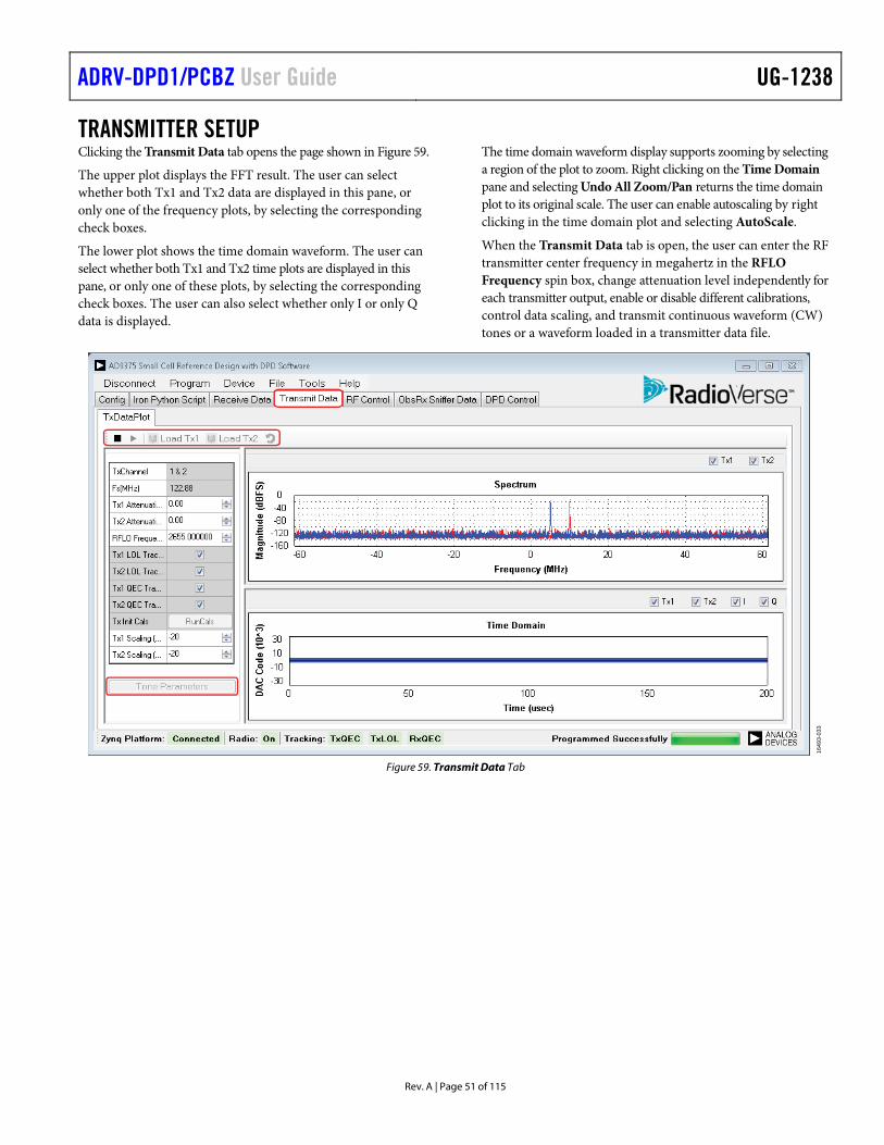
ADRV-DPD1/PCBZ User Guide UG-1238
Rev. A | Page 51 of 115
TRANSMITTER SETUP Clicking the Transmit Data tab opens the page shown in Figure 59.
The upper plot displays the FFT result. The user can select whether both Tx1 and Tx2 data are displayed in this pane, or only one of the frequency plots, by selecting the corresponding check boxes.
The lower plot shows the time domain waveform. The user can select whether both Tx1 and Tx2 time plots are displayed in this pane, or only one of these plots, by selecting the corresponding check boxes. The user can also select whether only I or only Q data is displayed.
The time domain waveform display supports zooming by selecting a region of the plot to zoom. Right clicking on the Time Domain pane and selecting Undo All Zoom/Pan returns the time domain plot to its original scale. The user can enable autoscaling by right clicking in the time domain plot and selecting AutoScale.
When the Transmit Data tab is open, the user can enter the RF transmitter center frequency in megahertz in the RFLO Frequency spin box, change attenuation level independently for each transmitter output, enable or disable different calibrations, control data scaling, and transmit continuous waveform (CW) tones or a waveform loaded in a transmitter data file.
1649
3-03
3
Figure 59. Transmit Data Tab

UG-1238 ADRV-DPD1/PCBZ User Guide
Rev. A | Page 52 of 115
TRANSMIT DATA OPTIONS The SCES provides the following options for inputting transmitter data:
• A single tone or dual tone signal can be generated by the evaluation system using the ToneParameters dialog box, as shown in Figure 60. In this box, the user can select the number of tones (one or two) that are transmitted on the selected transmitter output. The user has control over the tone frequency offset relative to the LO frequency, as well as the tone amplitude(s) in decibels relative to full scale. The user can store those signals in the form of text files by clicking Save Tx Raw Data into a File. Click the play button in the toolbar before data is populated into these files.
• User generated data files can be selected by clicking Load Tx1 and Load Tx2. • Format these files as I sample <TAB> and Q sample
<NEW_LINE> per line. Each I or Q sample must be an integer in the range between +32,768 to −32,767.
• If peak values of I and Q samples are very low, the signal can be normalized to full scale using the Scaling Required check box in the Load window.
• File size is limited to four megasamples (MS) for each channel (I data = 4 MS maximum, Q data = 4 MS maxi-mum). The EVAL-TPG-ZYNQ3 allocates 134,217,728 bytes for each buffer. Rx1, Rx2, observation receiver, Tx1, and Tx2 have separate buffers. Each data path uses 4 bytes per complex sample (16 bits for the I sample and 16 bits for the Q sample). Therefore, each data path has 33,554,432 16-bit I/Q pairs. A 122.88 MSPS I/Q rate therefore translates to a maximum of just over 273 ms of capture time for each channel.
Clicking the play button on the toolbar starts signal transmission on the AD9375 Tx1 and/or Tx2 outputs. Clicking play starts a process in which the generated CW data or the I/Q waveform data in the Tx1 and Tx2 files are sent to the AD9375. The data is loaded into the random access memory (RAM) of the EVAL-TPG-ZYNQ3, and a RAM pointer loops through the data continuously until the user clicks stop on the toolbar.
The Tx1 Attenuation (dB) spin box allows the user to control analog attenuation in the Tx1 channel. The Txl Attenuation (dB) spin box provides 0.05 dB of attenuation control resolution. The Tx2 Attenuation (dB) spin box performs the same operation on the Tx2 channel.
The Tx1 Scaling (dBFS) spin box allows the user to control digital scaling of data sent over the Tx1 channel. The scaling can be set in 1 dB increments. Scaling is only available for transmitter data loaded using the Load Tx1 button. The Tx2
Scaling (dBFS) box performs the same operation on the data sent over the Tx2 channel. It is recommended to apply some of this digital scaling to a signal that is close to full scale (0 dBFS) when DPD is applied, which allows for gain expansion of the signal.
The Tx1 LOL Tracking check box enables transmitter LOL tracking calibration. Calibration improves the LOL performance on the Tx1 channel. The Tx2 LOL Tracking check box performs the same operation on the Tx2 channel. To perform Tx LOL tracking calibrations, circuitry external to the AD9375 is required to route the transmitter signal back to the observation receiver input. The SCRD radio has this circuitry.
The Tx1 QEC Tracking check box enables transmitter QEC tracking calibration on the Tx1 channel. Calibration improves the analog quadrature modulator performance of the AD9375. The Tx2 QEC Tracking check box performs the same operation on the Tx2 channel.
Tx1 and Tx2 LOL and QEC tracking calibrations can operate only when the observation receiver path is configured to be used with internal calibration. When the user enables transmitter outputs, the AD9375 SCES automatically reconfigures the observation receiver path to the internal calibration mode. The user can change the observation receiver path at any time using the ObsRx Sniffer Data tab. Refer to the AD9375 Design File Package for details on calibration.
The Tx Init Cals button runs transmitter initialization QEC and LOL calibrations. It is recommended to run these calibrations first, before the user starts to transmit signals. While the initial calibrations are running, high level tones are present at the AD9375 transmitter outputs. Therefore, it is recommended to disable the PA until this calibration finishes.
Both of the AD9375 transmitter outputs are recommended to be terminated with 50 Ω loads during the initial calibration process.
1649
3-03
4
Figure 60. Transmitter ToneParameters Dialog Box

ADRV-DPD1/PCBZ User Guide UG-1238
Rev. A | Page 53 of 115
RF PATH AND DPD CONTROLS By default, the transmitter output RF paths and the Rx input RF paths are disabled. To configure and enable the RF paths, use the RF Control and DPD Control tabs.
TRANSMITTER RF PATH CONTROLS Each transmitter RF path features a gain amplifier with a built in step attenuator and a PA, as shown in Figure 10. The RF Control tab features the controls to enable or disable the amplifiers and to set the digital step attenuator, as shown in Figure 61.
The minimum attenuation that can be set is 0 dB. The maximum attenuation depends on the device fitted as the gain amplifier. For example, radio boards with ADL5335 gain amplifiers exhibit an attenuation range of 0 dB to 20 dB in 0.5 dB increments.
RECEIVER RF PATH CONTROLS Each receiver RF path features an LNA, as shown in Figure 10. The LNAs for Rx1 and Rx2 can be independently enabled or disabled by clicking the respective button in the RF Control tab, shown in Figure 61.
1649
3-03
5
Figure 61. RF Control Tab
UG-1238 ADRV-DPD1/PCBZ User Guide
Rev. A | Page 54 of 115
DPD CONTROLS The AD9375 transceiver features a low power DPD algorithm that runs on-chip on an ARM processor. This feature can be enabled or disabled via the DPD controls on the DPD Control tab, as shown in Figure 62.
To enable the DPD feature, select the transmitter path(s) for which linearization is required by selecting the Tx1 Dpd Adaptation and Tx2 Dpd Adaptation check boxes, then enable DPD tracking by clicking Start DPD.
To disable the DPD feature for a transmitter path, select the check box for the transmitter path that no longer requires linearization and disable DPD tracking by clicking Reset DPD.
Note that DPD can only be used after the initial calibrations are done, while the transmitter is enabled, while the waveform playback is running, and while the gain amplifier and PA are both enabled.
1649
3-03
7
Figure 62. DPD Control Tab

ADRV-DPD1/PCBZ User Guide UG-1238
Rev. A | Page 55 of 115
SCRIPTING After the user configures the device to the desired profile, a script can be generated with all API initialization calls in the form of IronPython functions. The Tools > Create Script > Python command can be used to accomplish this task. See the Tools Dropdown Menu section for more details.
The Iron Python Script tab allows the user to use the IronPython language to write a unique sequence of events and then execute them using the ADRV-DPD1/PCBZ system.
Scripts generated using the Tools > Create Script > Python command can be loaded, modified if needed, and run in the Iron Python Script tab. Figure 63 shows the Iron Python Script tab after executing the File > New command in the Iron Python Script tab. The top pane contains IronPython script commands, and the bottom pane of the window displays the script output.
The Iron Python Script tab provides the user with a number of options to manipulate the editing and execution of the IronPython scripts. The File dropdown menu in the Iron Python Script tab, shown in Figure 64, contains the following commands:
• New creates a new IronPython script that connects to the AD9375 small cell reference system and checks the AD9375 API version operating on the EVAL-TPG-ZYNQ3.
• Load allows the user to load previously stored IronPython scripts.
• Save and Save As allow the user to store IronPython scripts. • Close closes the currently active Iron Python Script tab
without saving.
1649
3-03
9
Figure 63. Iron Python Script Tab

UG-1238 ADRV-DPD1/PCBZ User Guide
Rev. A | Page 56 of 115
1649
3-04
0
Figure 64. File Menu in the Iron Python Script Tab
1649
3-04
1
Figure 65. Build Menu in the Iron Python Script Tab
The Build dropdown menu in the Iron Python Script tab, shown in Figure 65, contains the following commands:
• Run executes the IronPython script open in the currently active Iron Python Script tab using the ADRV-DPD1/PCBZ. Script output is displayed at the bottom of the Iron Python Script tab.
• Clear Script clears the IronPython script editing pane. • Clear Output clears the IronPython script output pane.
IRONPYTHON SCRIPT EXAMPLE The following example, which is generated by executing the File > New command in the IronPython Script tab, connects to the AD9375 small cell reference system and then checks and displays the version of the AD9375 API operating on the EVAL-TPG-ZYNQ3.
When using the Iron Python Script tab, the user can execute any API command.
The list of all API commands is provided by the SCES. The list can be viewed by clicking DLL Help File in the Help menu. All AD9375 API functions, when called in the Iron Python Script
tab, must be renamed according to the Mykonos API syntax, such as MYKONOS_functionName(), to reflect the IronPython syntax, Mykonos.functionName().
A header with a new class instance for a new connection must be added. For example, after calling #Create an Instance of the Class
Link = AdiCommandServerClient.Instance
The new class instance for the AD9375 evaluation hardware is Link.
An example of an API function called using IronPython follows. If the user wants to check the gain index for the Rx1 signal chain using the AD9375 API function called MYKONOS_getRx1Gain()
The user calls the following IronPython function: print Link.Mykonos.getRx1Gain()
This call assumes that the platform is initialized using the example code described in this section.

ADRV-DPD1/PCBZ User Guide UG-1238
Rev. A | Page 57 of 115
########################
#ADI Demo Python Script
########################
#Import Reference to the DLL
import clr
clr.AddReferenceToFileAndPath("C:\\Program Files (x86)\\Analog Devices\\Small Cell Evaluation Software\\AdiCmdServerClient.dll"")
from AdiCmdServerClient import AdiCommandServerClient
from AdiCmdServerClient import Mykonos
#Create an Instance of the Class
Link = AdiCommandServerClient.Instance
#Connect to the Zynq Platform
if(Link.hw.Connected == 1):
Connect = 0
else:
Connect = 1
Link.hw.Connect("192.168.1.10", 55555)
#Read the Version
print Link.version()
#Disconnect from the Zynq Platform
if(Connect == 1):
Link.hw.Disconnect()

UG-1238 ADRV-DPD1/PCBZ User Guide
Rev. A | Page 58 of 115
TROUBLESHOOTING This section provides a quick help guide with a description of what to do if the system is not operational. This guide assumes that the user followed all the instructions and that the hardware configuration matches the one described in this user guide.
STARTUP No LED Activity (Zynq)
If there is no LED activity on the EVAL-TPG-ZYNQ3 board,
1. Check if the EVAL-TPG-ZYNQ3 is properly powered. There must be 12 V present at the J22 input, and after powering the EVAL-TPG-ZYNQ3 on (with SW1 turned on), the following must be true:
• The fan on the EVAL-TPG-ZYNQ3 is active. • A number of green LEDs on the EVAL-TPG-ZYNQ3
near SW1 are on with no red LEDs active on the EVAL-TPG-ZYNQ3.
EVAL-TPG-ZYNQ3 GPIO LEDs follow the sequence described in the Hardware Operation section.
2. If the LED sequence does not follow the one described, check the jumper settings and SW11 positions on the EVAL-TPG-ZYNQ3. If the jumper settings are correct, check that the SD card is properly inserted into the socket (J30). It is recommended to use the SD card provided with the evaluation system. The SD card can be updated to the appropriate image that is available in the SCES under Device > Update > Platform Files.
If there is still a problem and the user is certain that the EVAL-TPG-ZYNQ3 is operational, contact an Analog Devices representative for assistance.
LEDs Active but SCES Reports that Hardware is Not Connected
If the SCES reports that the hardware is not connected,
1. Check if the Ethernet cable is properly connected to the PC used to run the SCES and the EVAL-TPG-ZYNQ3. LEDs on the EVAL-TPG-ZYNQ3 next to the Ethernet socket flash when the connection is active.
2. If the Ethernet cable is properly connected, check that the Windows operating system (OS) is able to communicate
over the Ethernet port with the EVAL-TPG-ZYNQ3. Check if the IP address and open ports for the Ethernet connection used to communicate with the EVAL-TPG-ZYNQ3 follow the advice provided in the SCES Setup section.
3. Run cmd.exe on the Windows OS and type ping 192.168.1.10. The user can see a reply from the EVAL-TPG-ZYNQ3. If no reply is received, reexamine the connection with the EVAL-TPG-ZYNQ3.
4. If a connection with the EVAL-TPG-ZYNQ3 is established but SCES still reports that the hardware is not available, ensure that Port 22 (secure shell (SSH)) and Port 55555 (evaluation software) are not blocked by firewall software on the Ethernet connection used to communicate with the EVAL-TPG-ZYNQ3. Both ports must be open for normal operation. Refer to the SCES Setup section for more details.
LED 1 and LED 2 (STATUS 1 and STATUS 0) on Interposer Board Do Not Illuminate After Programming
If one or more of the status LEDs on the interposer board do not illuminate,
1. Check if the clock is set up properly on the external reference clock.
2. Ensure the clock is connected properly to J8 or J13 and to the reference out connection on the external clock device.
3. In the Ref Clock Setup tab, check that the frequency in the Ref A or Ref B box is the same as the reference clock, and the selected Ref Clock Selection option button is the same as the connector being used on the interposer board to receive the clock signal (see the Clock Setup section for details).
ERROR HANDLING The SCES provides the user with a number of error messages in case there are problems with the hardware or software configuration. The error messages the SCES can display are intended to provide a description of the problem encountered by the software. If the error description refers to the DLL command, refer to the API and DLL help files supplied with the SCES.

ADRV-DPD1/PCBZ User Guide UG-1238
Rev. A | Page 59 of 115
TYPICAL PERFORMANCE Figure 66, Figure 67, Figure 68, and Figure 69 show typical transmitter adjacent channel leakage power ratio (ACLR) performance of the ADRV-DPD1/PCBZ radio board. The difference between the DPD turned on and off is shown in the improved ACLR performance when DPD is enabled on these 5 MHz and 20 MHz bandwidth LTE carriers.
–65
–75
–55
–45
–35
–25
–15
–5
5
2.63
7
POW
ER (d
B)
FREQUENCY (GHz)
2.64
0
2.64
2
2.64
5
2.64
7
2.65
0
2.65
2
2.65
5
2.65
7
2.66
0
2.66
2
2.66
5
2.66
7
2.67
0
2.67
2
DPD ONDPD OFF
1649
3-26
6
Figure 66. Tx1 5 MHz ACLR
–65
–75
–55
–45
–35
–25
–15
–5
5
2.60
POW
ER (d
B)
2.61
2.62
2.63
2.64
2.65
2.66
2.67
2.68
2.69
2.70
2.71
DPD ONDPD OFF
1649
3-26
7
FREQUENCY (GHz) Figure 67. Tx1 20 MHz ACLR
–65
–75
–55
–45
–35
–25
–15
–5
5
2.63
7
POW
ER (d
B)
2.64
0
2.64
2
2.64
5
2.64
7
2.65
0
2.65
2
2.65
5
2.65
7
2.66
0
2.66
2
2.66
5
2.66
7
2.67
0
2.67
2
DPD ONDPD OFF
1649
3-26
8
FREQUENCY (GHz) Figure 68. Tx2 5 MHz ACLR
–65
–75
–55
–45
–35
–25
–15
–5
5
2.60
POW
ER (d
B)
2.61
2.62
2.63
2.64
2.65
2.66
2.67
2.68
2.69
2.70
2.71
DPD ONDPD OFF
1649
3-26
9
FREQUENCY (GHz) Figure 69. Tx2 20 MHz ACLR
Power measured is the total channel power of the 4.515 MHz or 18.015 MHz channels relative to the transmit channel power. All measurements are taken on a transmitted signal with a transmit power of 24 dBm at the antenna connector. The test waveforms were 3GPP E-TM1.1, 7.0 dB peak to mean −11 dBFS rms, centered on the transmitter LO.
Table 12. Tx1 5 MHz DPD Off ACLR Offset (MHz) Power (dBc) −15 −63.8 −10 −52.4 −5 −39.6 +5 −41.1 +10 −53.0 +15 −63.7
Table 13. TX1 5 MHz DPD On ACLR Offset (MHz) Power (dBc) −15 −67.4 −10 −63.1 −5 −60.1 +5 −59.1 +10 −62.5 +15 −66.9
Table 14. TX1 20 MHz DPD Off ACLR Offset (MHz) Power (dBc) −40 −54.6 −20 −38.8 +20 −42.1 +40 −54.4
Table 15. TX1 20 MHz DPD On ACLR Offset (MHz) Power (dBc) −40 −62.5 −20 −57.3 +20 −57.3 +40 −64.6

UG-1238 ADRV-DPD1/PCBZ User Guide
Rev. A | Page 60 of 115
Table 16. TX2 5 MHz DPD Off ACLR Offset (MHz) Power (dBc) −15 −64.2 −10 −53.4 −5 −39.7 +5 −41.1 +10 −53.7 +15 −63.9
Table 17. TX2 5 MHz DPD On ACLR Offset (MHz) Power (dBc) −15 −68.5 −10 −64.5 −5 −59.7 +5 −59.5 +10 −64.4 +15 −68.2
Table 18. TX2 20 MHz DPD Off ACLR Offset (MHz) Power (dBc) −40 −55.2 −20 −39.0 +20 −41.5 +40 −53.8
Table 19. TX2 20 MHz DPD On ACLR Offset (MHz) Power (dBc) −40 −63.0 −20 −57.0 +20 −55.6 +40 −64.0
ELECTRICAL SPECIFICATIONS
Table 20. General TA = 25°C, VDD = 5.1 V, 50 Ω System
Parameter Value
Unit Test Conditions Min Typ Max Frequency and Bandwidths
RF Transmitter Frequency Range 2620 2690 MHz Tx 2500 2570 MHz Rx
RF Bandwidth 40 MHz Environmental
Operational Temperature 0 351 °C 1 Maximum operational temperature refers to temperature in still air with heatsink supplied. Other heatsinking arrangements are possible.
Table 21. RF Performance TA = 25°C, VDD = 5.1 V, 50 Ω System
Parameter Value
Unit Test Conditions Min Typ Max Transmitter Specification
Maximum Transmitter Output Power1 24 dBm 20 MHz bandwidth, LTE E-TM1.1, peak to average power ratio (PAR) = 7 dB
Transmitter Output Power Accuracy 0.025 dB ACLR at 20 MHz Offset 47 52 dBc 20 MHz bandwidth, LTE E-TM1.1, O/P = 24 dBm, PAR = 7 dB Error Vector Magnitude (EVM)2 4.8 % 20 MHz bandwidth, LTE E-TM3.1 (64 QAM), PAR = 7 dB
Receiver Specification Receiver Noise Figure 7.9 10.7 dB 2535 MHz Receiver Front End Gain 6 9 dB Antenna port to AD9375 Receiver AD9375 Gain 30 dB AD9375
1 Output power at each antenna port. 2 EVM measured with specific crest factor reduction algorithm.

ADRV-DPD1/PCBZ User Guide UG-1238
Rev. A | Page 61 of 115
BILL OF MATERIALS Table 22. ADRV-DPD1/PCBZ Electrical Bill of Materials Designator Description Manufacturer Part Number C1, C3, C5, C9, C144, C145, C198, C199, C200, C201 Capacitors, 0201, 100 pF,
50 V, C0G, ±5% Murata GRM0335C1H101JD01D
C2, C7 Capacitors, 0201, 0.5 pF, 25 V, C0G, ±0.1 pF
Murata GJM0335C1ER50BB01D
C4, C8, C197, C205 Capacitors, 0201, 1.0 pF, 25 V, C0G, ±0.1 pF
Murata GJM0335C1E1R0BB01D
C6, C10, C12, C14 Capacitors, 0201, 6.0 pF, 25 V, C0G, ±0.5 pF
Murata GJM0335C1E6R0DB01D
C11, C13 Capacitors, 0201, 5.6 pF, 25 V, C0G, ±0.5 pF
Murata GJM0335C1E5R6DB01D
C15, C21, C24, C26, C27, C30, C33, C34, C37, C41, C43, C45, C50, C52, C54, C55, C57, C58, C59, C60, C62, C64, C81, C82, C110, C134, C143, C152, C153, C158, C159, C214
Capacitors, 0402, 1.0 μF, 10 V, X5R, ±10%
Murata GRM155R61A105KE15D
C16, C70, C74, C122, C141, C150, C167 Capacitors, 0603, 10 μF, 10 V, X5R, ±10%
Murata GRM188R61A106KE69D
C17, C18, C19, C20, C22, C23, C25, C28, C29, C35, C38, C39, C40, C42, C48, C49, C51, C53, C56, C61, C63, C66, C67, C71, C75, C108, C132, C139, C147, C211, C215
Capacitors, 0201, 0.10 μF, 10 V, X5R, ±10%
Murata GRM033R61A104KE84D
C31 Capacitors, 0201, 1000 pF, 25 V, X7R, ±10%
Murata GRM033R71E102KA01D
C32, C36, C46, C47, C65, C68, C69, C213 Capacitors, 0805, 100 μF, 4 V, X5R, ±20%
Murata GRM21BR60G107ME15
C44, C168, C212 Capacitors, 0201, 10000 pF, 10 V, X7R, ±10%
Murata GRM033R71A103KA01D
C72, C76, C84, C91, C96, C99, C113, C123, C126, C129, C138, C160, C171, C175, C203
Capacitors, 0402, 0.10 μF, 16 V, X5R, ±10%
Murata GRM155R61C104KA88D
C73, C83 Capacitors, 1206, 100 μF, 10 V, X5R, ±20%
TDK C3216X5R1A107M160AC
C77, C78, C79, C80, C86, C87, C88, C89, C94, C95, C109, C125, C131, C133, C156, C157, C164, C166, C169, C170
Capacitors, 0805, 47 μF, 10 V, X5R, ±20%
Murata GRM21BR61A476ME15D
C85, C92, C98, C106 Capacitors, 0805, 10 μF, 25 V, X5R, ±10%
Murata GRM219R61E106KA12D
C90, C93, C101, C102, C111, C112, C120, C121, C135, C136, C165, C208
Capacitors, 0402, 3300 pF, 50 V, X7R, ±10%
Murata GRM155R71H332KA01D
C97, C100 Capacitors, 0402, 2200 pF, 50 V, X5R, ±10%
Murata GRM155R61H222KA01D
C105, C115, C116, C127, C140, C146, C162, C163, C173, C174, C182, C183, C188, C189, C190, C191, C220, C221
Capacitors, 0402, 8.2 pF, 50 V, C0G, ±0.1 pF
Murata GJM1555C1H8R2BB01D
C107, C114, C118, C119, C124, C128, C130, C137, C148, C149, C155, C161, C172, C178, C179, C180, C181, C184, C185, C186, C187, C202, C206, C207
Capacitors, 0402, 100 pF, 50 V, C0G, ±5%
Murata GRM1555C1H101JA01D
C117, C154, C222, C223 Capacitors, 0201, 4.3 pF, 25 V, C0G, ±0.25 pF
Murata GJM0335C1E4R3CB01D
C176, C177 Capacitors, 0603, 0.10 μF, 50 V, X7R, ±10%
Murata GRM188R71H104KA93D
C192, C193, C194, C195 Capacitors, 0201, 8.2 pF, 25 V, C0H, ±0.5 pF
Murata GJM0336C1E8R2DB01D
C216, C217, C218, C219 Capacitors, 0402, 1.3 pF, 50 V, C0G, ±0.1 pF
Murata GJM1555C1H1R3BB01D
D2, D3 Surface mount limiter diodes, 75 V
Skyworks CLA4606-085LF
J1 100-position connector header
SAMTEC ERM8-050-02.0-S-DV-K-TR

UG-1238 ADRV-DPD1/PCBZ User Guide
Rev. A | Page 62 of 115
Designator Description Manufacturer Part Number J3, J4 SMP RF connectors, PCB
Straight receptacle, 4 solder legs
Radiall R222 426 300
L1, L2 Inductors, 0201, 3.9 nH, ±0.1 nH
Murata LQP03TN3N9B02P
L3, L4 Inductors, 0201, 6.2 nH, ±3% Murata LQP03TN6N2H02P L6, L30 Inductors, 0402, 36 nH, ±2% Murata LQW15AN36NG00 L7, L31 Inductors, 0402, 1.0 nH,
±0.3 nH Murata LQG15HN1N0S02
L8, L32 Inductors, 0402, 30 nH, ±2% Murata LQW15AN30NG00 L10, L11 Ferrites, 0201, 33 Ω, ±25% Murata BLM03PX330SN1 L12, L18, L21, L23, L26 Ferrites, 0402, 120 Ω, ±25% Murata BLM15PX121SN1D L13, L15 Inductors, 0201, 10 nH, ±3% Murata LQP03TN10NH02P L14, L19, L20, L22, L25, L52, L66, L70 Ferrites, 0402, 470 mΩ,
±25% Murata BLM15PX471SN1D
L16, L17 Inductors, 0201, 27 nH, ±5% TDK MLK0603L27NJT000 L24, L51, L53 Ferrites, 0402, 220 Ω, ±25% Murata BLM15PX221SN1D L27, L37, L38, L39 Ferrites, 0603, 120 Ω, ±25% Murata BLM18KG121TN1D L28, L29 Inductors, 2.5 × 2.0 × 1.2,
2.2 μH, ±20% Toko 1239AS-H-2R2M
L33, L34, L40, L41, L55, L56, L57, L59, L60, L61, L67, L71, L78, L79, L80, L81
Ferrites, 0402, 33 Ω, ±25% Murata BLM15PX330SN1D
L35, L36 Inductors, 4020, 1 µH, ±20% Coilcraft XFL4020-102MEC L42, L43 Inductors, 0402, 24 nH, ±2% Murata LQW15AN24NG00 L44, L45, L46, L47 Inductors, 0402, 27 nH, ±5% Murata LQW15AN27NJ00 L48 Ferrite, 0805, 33 Ω, ±25% Tayio Yuden FBMJ2125HM330-T L54, L62 Inductors, 0402, 8.2 nH, ±2% Murata LQW15AN8N2G00D L58, L63 Inductors, 0402, 4.7 nH,
±0.1 nH Murata LQW15AN4N7B00D
L85, L87 Inductors, 0402, 2.7 nH, ±0.1 nH
Murata LQW15AN2N7B00D
Q1 Dual N-channel 20 V (D-S) MOSFET
Vishay SiA906EDJ-T1-GE3
R1 Resistor, 0201, 100 Ω, thick film, ±1%
Rohm MCR006YZPF1000
R2, R6, R87, R92, R109, R131, R147, R148 Resistors, 0402, 4.7 kΩ, thick film, ±1%
Rohm MCR01MZPF4701
R4 Resistor, 0402, 1 kΩ, thick film, ±1%
Rohm MCR01MZPF1001
R5 Resistor, 0402, 14.3 kΩ, thick film, ±1%
Rohm MCR01MZPF1432
R7, R8, R15, R23, R47, R52, R56, R76, R85, R88, R89, R91, R104, R105, R106, R107, R108, R113, R116, R132, R133
Resistors, 0402, 10 kΩ, thick film, ±1%
Rohm MCR01MZPF1002
R9, R14, R20, R21, R32, R33, R35, R36, R42, R43, R54, R69, R110, R111, R114, R125, R126, R137, R140, R143, R144, R146
Resistors, 0402, 0 Ω, thick film
Rohm MCR01MZPJ000
R10 Resistor, 0402, 15 kΩ, thick film, ±1%
Rohm MCR01MZPF1502
R11, R22, R27 Resistors, 0402, 10 kΩ, thick film, ±0.5%
Yageo RT0402DRD0710KL
R17, R94, R112, R117, R124, R135 Resistors, 0402, 100 kΩ, thick film, ±1%
Rohm MCR01MZPF1003
R18 Resistor, 0402, 31.6 kΩ, thick film, ±0.5%
Yageo RT0402DRD0731K6L
R19, R26 Resistor, 0402, 22 kΩ, thick film, ±1%
Rohm MCR01MZPF2202
R24, R34, R39, R57, R58, R62, R64, R74 Resistors, 0201, 0 Ω, thick film
Rohm MCR006YZPJ000

ADRV-DPD1/PCBZ User Guide UG-1238
Rev. A | Page 63 of 115
Designator Description Manufacturer Part Number R25 Resistor, 0402, 13 kΩ, thick
film, ±0.5% Yageo RT0402DRD0713KL
R29 Resistor, 0402, 10.2 kΩ, thick film, ±0.5%
Yageo RT0402DRD0710K2L
R40, R72, R93, R121 Resistors, 0402, 2.2 kΩ, thick film, ±1%
Rohm MCR01MZPF2201
R41, R45 Resistors, 0402, 18 Ω, thick film, ±1%
Rohm MCR01MZPF18R0
R44, R48, R49, R60 Resistors, 0402, 294 Ω, thick film, ±1%
Rohm MCR01MZPF2940
R46, R66 Resistors, 0402, 105 Ω, thick film, ±1%
Rohm MCR01MZPF1050
R50, R65 Resistors, 0603, 49.9 Ω, thick film, ±1%
Rohm MCR03EZPFX49R9
R51, R53, R67, R68 Resistors, 0402, 78.7 Ω, thick film, ±1%
Rohm MCR01MZPF78R7
R55, R70, R77, R90 Resistors, 0402, 8.2 kΩ, thick film, ±1%
Rohm MCR01MZPF8201
R59, R78 Resistors, 0402, 12 Ω, thick film, ±1%
Rohm MCR01MZPF12R0
R61, R63, R81, R83 Resistors, 0402, 430 Ω, thick film, ±1%
Rohm MCR01MZPF4300
R127, R128 Resistors, 0402, 6.34 kΩ, thick film, ±0.5%
Yageo RT0402DRD076K34L
T2, T5 Ultra low profile 0805 baluns 50 Ω to 50 Ω balanced
Anaren B0322J5050AHF
T3, T6 Ultra low profile 0805 baluns 50 Ω to 200 Ω balanced
Anaren BD0826J50200AHF
U1 Integrated dual RF transceiver with observation
Analog Devices
AD9375BBCZ
U2 Low voltage temperature sensors
Analog Devices
TMP36GRTZ-REEL7
U3 Quad buck regulator integrated power solution
Analog Devices
ADP5054ACPZ
U4, U8 2655 MHz isolators (CW) TDK CU4S0506AT-2655-00 U5, U9 30 dB directional couplers Anaren X3C26P1-30S U6, U11 Band 7 UPD series duplexers CTS UPD007A U7, U15 Programmable gain
amplifiers (0.7 GHz to 3.4 GHz) Analog Devices
ADL5335ACPZ
U10, U14 2490 MHz to 2690 MHz power amplifiers
Skyworks SKY66297-11
U12, U13 200 MHz to 3800 MHz broad-band low noise amplifiers
Skyworks SKY67159-396LF
U16, U21 RF filters for small cells (2535 MHz)
TDK B9629
U17, U18 Buffers with open drain outputs
NXP 74LVC2G07GW
U19 Inverters with open drain outputs
NXP 74LVC2G06GW
U20, U22 RF low-pass filters TDK DEA162690LT-5051B1 U23 128 kB SPI CMOS serial
EEPROM, TSSOP-8 On-Semi CAT25128YI-GT3
SH1 ADI RF card bottom shieldcan
Benetel 31082267
SH2 ADI RF card top shieldcan Benetel 31082268 SH3 ADI RF card PSU shieldcan Benetel 31082269

UG-1238 ADRV-DPD1/PCBZ User Guide
Rev. A | Page 64 of 115
Designator Description Manufacturer Part Number PCB1 AD9375 small cell reference
design PCB_REV1.3 Benetel 31282247
HW1, HW2, HW3, HW4 PCB adhesive, applied to U6 and U11
RS 567-581
Table 23. ADRV-DPD1/PCBZ Mechanicals Bill of Materials Designator Description Manufacturer Part Number HW5, HW6, HW7 Screws, M3, 16 mm long pozi pan Duratool 1420393 HW8, HW9, HW10, HW11 Screws, M3, steel, 6 mm, bright zinc, flat/countersunk head pozidriv Duratool 1420397 HW12, HW13, HW14 Washers, plain, M3 Duratool 1377551 HW15, HW16, HW17 Washers, lock, M3 Duratool 1624024 HW18 Heatsink, machining Benetel 31082282 HW19 Heatsink, interface Benetel 31082283 HW20 Thermal compound, syringe, 10 ML Fischer Elektronik WLPK 10 HW21 Gap pad Benetel 31082284 HW22, HW23 Gap pads Benetel 31082285 HW24 EMC gasket Benetel 31082287 H25, H26, H27 Standoffs and spacers, 9 mm RAF Electronic Hardware M0538-3-AL
Table 24. ADRV-DPD1/PCBZ Empty Pads (Do Not Fit) Designator Description C103, C104, C142, C151, C196, C204, C209, C210 Capacitors, 0201 L72, L73, L75, L76, L84, L86 Inductors, 0402 R73, R75, R82, R84, R86, R95 Resistors, 0201 R12, R13, R28, R30, R31, R37, R38, R71, R97, R98, R100, R101, R136, R138, R139, R141 Resistors, 0402 R3, R16 Resistors, 0603
Table 25. ADRV-INTERPOS1/PCBZ Electrical Bill of Materials Designator Description Manufacturer Part Number C1, C39, C54, C56, C57, C58, C59, C60, C63, C64,
C83, C86, C88, C89, C116, C127, C128, C129, C130, C132
Capacitors, 0402, 1.0 μF, 6.3 V, X5R Murata GRM155R60J105KE19D
C2, C3, C4, C5, C6, C7, C8, C9, C10, C11, C12, C13, C14, C15, C16, C17, C18, C19, C20, C25, C26, C40, C46, C52, C53, C65, C69, C76, C81, C90, C91, C92, C93, C94, C95, C96, C97, C98, C99, C100, C101, C102, C103, C104, C105, C106, C107, C115, C117, C125
Capacitors, 0402, 0.1 μF, 16 V, X7R Murata GRM155R71C104KA88D
C21, C28, C29, C62, C113, C123 Capacitors, 0402, 0.01 μF, 25 V, X5R TDK C1005X5R1E103K050BA C22, C66, C67, C68, C77, C78, C80, C82, C84, C85 Capacitors, 0805, 10 μF, 25 V, X5R TDK C2012X5R1E106M C23, C33, C41, C50 Capacitors, 0402, 1000 pF, 50 V, C0G Murata GRM1555C1H102JA01D C30, C32 Capacitors, 0402, 470 pF, 50 V, C0G Murata GRM1555C1H471GA01D C34, C35, C43, C44 Capacitors, 1206, 100000 pF, 50 V,
C0G Murata GRM31C5C1H104JA01
C36 Capacitors, 0603, 0.47 μF, 16 V, X7R Murata GCM188R71C474KA55D C37, C70, C79 Capacitors, 0402, 3900 pF, 10 V, C0G Murata GRM1557U1A392JA01D C38, C48, C49, C55, C71, C72, C73, C74, C75, C108,
C109, C110, C111, C112, C114, C119 Capacitors, 1210, 47 μF, 16 V, X5R Murata GRM32ER61C476ME15L
C45 Capacitor, 0603, 1500 pF, 50 V, C0G Murata GRM1885C1H152JA01D C47 Capacitor, 0402, 1 μF, 25 V, X6S Murata GRM155C81E105KE11 C51, C118 Capacitors, 1206, 0.1 μF, 50 V, C0G Murata GRM31C5C1H104JA01L C61 Capacitor, polarized, 100 μF, 25 V Panasonic EEE-FC1E101P

ADRV-DPD1/PCBZ User Guide UG-1238
Rev. A | Page 65 of 115
Designator Description Manufacturer Part Number D1, D4, D5 Diodes, Schottky, 40 V, 5 A surface
mount SMC On Semiconductor MBRS540T3G
D2 Diode, Schottky, 30 V, 5 A surface mount
Micro Commercial Components
SK53A-LTP
D3 TVS DIODE 13 VWM 27.2 VC SMB STMicroelectronics SMBJ13A-TR F1 Surface mount fuse, 5 A VFA
slimline, 1206 Littlefuse 0466005.NR
FB1, FB2, FB3, FB4, FB5, FB6, FB7, FB8, FB9 Ferrite, 120 Ω Murata BLM18KG121TN1D FL1 EMI network filter, 50 MΩ 25 V 15 A
EMIFIL Murata BNX016-01
J1, J2, J9, J10 Headers 2 × 8 0.1 inches SAMTEC TSW-108-08-G-D J3, J4, J8, J13 SMA connector jacks, female socket
50 Ω Cinch Technology 142-0701-201
J5, J6, J11, J12 MMCX vertical surface mount connectors
SAMTEC MMCX-J-P-H-ST-SM1
J7 20-position header, unshrouded connector 0.05 inches
SAMTEC FTSH-110-01-L-DV-K
J14 DC power connectors power jacks CUI PJ-102BH J15, J26 4-position 2.54 mm solder ST
through holes 10 A and contacts TE Connectivity 282834-4
J16 Header 2 × 3 0.1 inches SAMTEC TSW-103-08-G-D J20, J22 100-position connector headers SAMTEC ERF8-050-05.0-S-DV-K-TR J21 160-position board to board
connector SAMTEC ASP-134604-01
J23, J28 2-pin headers Amphenol Connex 69157-102 J24 400-position board to board
connector SAMTEC ASP-134488-01
L3 Inductor, 15 μH Coilcraft XAL4040-153MEB L4, L5 Inductor, 4.7 μH Coilcraft XAL6060-472MEB LED1, LED2, LED5, LED7, LED8, LED9, LED11 Green LEDs, 2.2 V, 0603 Rohm SML-310MTT86 LED12 Red LED, 1.8 V, 0603 Rohm SML-311UTT86 Q1, Q2 MOSFETs N-channel 20 V 12 A Vishay Siliconix SIA448DJ-T1-GE3 R2, R4, R5, R7, R9, R13, R14, R16, R18, R20, R28,
R29, R34, R36, R44, R49, R50, R71, R73, R74, R75, R76, R77, R79, R80, R81, R82, R83, R84, R85, R86, R87, R88, R92, R93, R125, R126, R128, R130, R134, R137, R139, R141, R145, R146, R149, R150, R152, R154, R155, R156, R157, R158, R159, R160, R162, R164, R165, R166, R167, R168, R169, R170, R172, R173, R174, R175, R176, R177, R178, R179, R180, R181, R182, R183, R184, R185, R186, R191, R199, R200, R201, R202, R203, R205, R207, R209, R218, R219, R220, R221, R261, R262, R263, R277, R278, R279, R280, R281, R282, R283, R284, R303, R317, R321, R322, R323, R324, R325, R328, R371, R372
Resistors, 0402, 0 Ω Rohm MCR01MZPJ000
R8, R10, R11, R15, R48, R136 Resistors, 0402, 100 Ω Rohm MCR01MZPF1000 R12 Resistor, 0402, 430 kΩ Rohm MCR01MZPF4303

UG-1238 ADRV-DPD1/PCBZ User Guide
Rev. A | Page 66 of 115
Designator Description Manufacturer Part Number R22, R25, R60, R65, R66, R67, R68, R69, R70, R97,
R108, R114, R118, R120, R123, R143, R147, R148, R161, R163, R171, R194, R197, R198, R204, R210, R212, R213, R214, R216, R217, R225, R226, R227, R228, R229, R230, R231, R232, R235, R240, R244, R245, R249, R254, R256, R257, R258, R259, R264, R265, R266, R267, R268, R272, R273, R274, R275, R285, R287, R288, R289, R290, R291, R292, R293, R294, R311, R312, R315, R316, R320, R326, R331, R332, R334, R335, R336, R337, R339, R340, R341, R342, R343, R344, R345, R346, R347, R348, R349, R350, R351, R352, R355, R356, R357, R358, R362, R363, R364, R365, R367, R368, R369, R370, R374, R376, R381, R382, R383, R384, R385
Resistors, 0402, 10 kΩ Rohm MCR01MZPF1002
R23, R24 Resistors, 0402, 390 Ω Rohm MCR01MZPF3900 R30, R43, R54, R58, R59, R61, R62, R64, R115, R117,
R121, R124, R153, R206, R208, R215, R233, R234, R250, R251, R252, R255, R271, R286, R314, R327, R329, R330, R333, R338, R353, R354, R359, R360, R361, R366, R375, R377
Resistors, 0402, 1 kΩ Rohm MCR01MZPF1001
R32, R99, R101, R188, R189 Resistors, 0402, 2.7 kΩ Rohm MCR01MZPF2701 R33, R100, R106, R127 Resistors, 0402, 51 kΩ Rohm MCR01MZPF5102 R40, R42 Resistors, 0402, 100 kΩ Rohm MCR01MZPF1003 R41, R91, R195, R196 Resistors, 1206, 0 Ω Rohm MCR18EZPJ000 R47, R56, R57, R72 Resistors, 0402, 1 MΩ Rohm MCR01MZPF1004 R63 Resistor, 0402, 332 Ω Rohm MCR01MZPF3320 R78, R96 Resistors, 0603, 1.0 kΩ Koa Speer RK73H1JTTD1001F R94, R241 Current sense resistors, 0.05 Ω Ohmite LVK12R050DER R95 Resistor, 1206, 1.5 kΩ Rohm MCR18EZPJ152 R98, R187 Resistors, 0402, 51.1 kΩ Panasonic ERA-2AEB5112X R103, R151 Resistors, 0402, 10 kΩ Vishay Dale TNPW040210K0BEED R104, R109 Resistors, 0402, 13 kΩ Rohm MCR01MZPF1302 R105, R111, R119, R192 Resistors, 0402, 200 Ω Rohm MCR01MZPF2000 R110 Resistor, 0402, 39 kΩ Panasonic ERA-2AEB393X R112 Resistor, 2512, 0.1 Ω Vishay Dale WSLT2512R1000FEA R113 Resistor, 0402, 3.9 kΩ Rohm MCR01MZPJ392 R122 Resistor, 0402, 220 Ω Rohm MCR01MZPF2200 R211 Resistor, 0402, 680 Ω Rohm MCR01MZPF6800 R319 Resistor, 0603, 0 Ω Rohm MCR03EZPJ000 T1, T2 4.5 MHz to 3000 MHz, 1:1
transmission line transformers Macom MABA-007159-000000
U1 IC clock generator, 1.25 GHz VCO Analog Devices AD9528BCPZ U2 Buffer, noninverting, 3 element,
1 bit per element Texas Instruments SN74LVC3G34DCUR
U3 General-purpose amplifier, 1 circuit, rail to rail
Analog Devices AD8605ARTZ
Y2 (U4) VCXO oscillator 122.880 MHz, 14 × 9 mm
Abracon ABLNO-V-122.880MHZ
U5 IC EEPROM 2 kB 400 KHz ST Microelectronics M24C02-WDW6TP U6, U13, U14, U18, U19, U21, U22, U35, U36, U37,
U38 Buffers and line drivers quad bus buffer gate
Texas Instruments SN74AUC125RGYR
U7 Single 2-input positive-OR gate Texas Instruments SN74LVC1G32DRL U8 Hex buffer/driver with open drain
output Texas Instruments SN74AUC07RGYR
U9, U11, U15, U23, U24, U25, U27, U28, U30, U31, U32, U33, U34
TVS diodes, 3.3 VWM, 17 VC Diodes Inc. D1213A-04SO-7
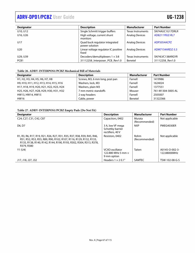
ADRV-DPD1/PCBZ User Guide UG-1238
Rev. A | Page 67 of 115
Designator Description Manufacturer Part Number U10, U12 Single Schmitt trigger buffers Texas Instruments SN74AUC1G17DRLR U16, U26 High voltage, current shunt
monitors Analog Devices AD8211YRJZ-RL7
U17 Quad buck regulator integrated power solution
Analog Devices ADP5054ACPZ
U20 Linear voltage regulator IC positive fixed
Analog Devices ADM7154ARDZ-3.3
U29, U39 Decoders/demultiplexers 1 × 3:8 Texas Instruments SN74LVC138ARGYR PCB1 31112258_Interposer_PCB_Rev1.0 Benetel 31112258_Rev1.0
Table 26. ADRV-INTERPOS1/PCBZ Mechanical Bill of Materials Designator Description Manufacturer Part Number H1, H2, H3, H4, H5, H6, H7, H8 Screws, M3, 6 mm long, pozi pan Farnell 1419986 H9, H10, H11, H12, H13, H14, H15, H16 Washers, lock, M3 Farnell 1624024 H17, H18, H19, H20, H21, H22, H23, H24 Washers, plain M3 Farnell 1377551 H25, H26, H27, H28, H29, H30, H31, H32 7 mm metric standoffs Mouser 761-M1304-3005-AL HW13, HW14, HW15 2 way headers Farnell 2505007 HW16 Cable, power Benetel 31322366
Table 27. ADRV-INTERPOS1/PCBZ Empty Pads (Do Not Fit) Designator Description Manufacturer Part Number C24, C27, C31, C42, C87 Capacitors, 0402 Murata
(Recommended) Not applicable
D6, D7 3 A, low VF mega Schottky barrier rectifiers, 40 V
NXP PMEG4030ER
R1, R3, R6, R17, R19, R21, R26, R27, R31, R35, R37, R38, R39, R45, R46, R51, R52, R53, R55, R89, R90, R102, R107, R116, R129, R132, R133, R135, R138, R140, R142, R144, R190, R193, R302, R304, R313, R378, R379, R380
Resistors, 0402 Rohm (Recommended)
Not applicable
Y1 (U4) VCXO oscillator 122.880 MHz 5 mm × 9 mm option
Taiten A0145-O-002-3-122.88000MHz
J17, J18, J27, J32 Headers 1 × 2 0.1" SAMTEC TSW-102-08-G-S

UG-1238 ADRV-DPD1/PCBZ User Guide
Rev. A | Page 68 of 115
INTERPOSER BOARD SCHEMATICS
QUAD BUCK REGULATOR
1-2 OFF3-4 AUTOMATIC5-6 ON
RED
1649
3-27
0
Figure 70. ADP5054 Connections
D3
F1123
J14
BIAS1
PSG3
CB 2
CG 4CG 6CG 5
FL1
DC POWERFILTER R95
1.5kΩ
VIN_DC
+12V INPUTFROM EXTERNAL PSU
TP21
C61100μF
D1
D2
LED5
R91
0Ω 5A
FMCA_VCC_12P0V
1649
3-27
1
Figure 71. Power Supply Connector

ADRV-DPD1/PCBZ User Guide UG-1238
Rev. A | Page 69 of 115
R98
51.1kΩ±0.1%
R302DNF
R107DNF
C7147μF
C72 C73 C74
FB6
120ΩR105200Ω
R99
2.7kΩ
R1012.7kΩ
1 2 3 4
J15
VCC_5V1_SENSE_B
FB1
SW1
DL1
12
DNF
J27
VCC_5V1_B
TERMINAL BLOCK FOREXTERNAL 5.1V INPUT
5.10V2.0A
C75
R241
0.05Ω
LED7
D4
C65
0.10μF
L5
4.7µH
R133DNF
U16ISENSE_5V1_B
R10310kΩ ± 0.1%
R781.0kΩS1
D1
S2
D2
D5
D4
G
D3
Q1
R195
0Ω
47μF 47μF 47μF47μF
+5.1
V
+5.1
V SE
NSE
GN
DG
ND
VIN+ 3
GND2
OUT1
V+
5
VIN– 4AD8211
FOR CORRECT CURRENT SENSEOPERATION, THE + AND – INPUTSMUST BE FLIPPED
1649
3-27
2
Figure 72. RF A Power Supply Connection

UG-1238 ADRV-DPD1/PCBZ User Guide
Rev. A | Page 70 of 115
R187
51.1kΩ ± 0.1%
R90DNF
R193DNF
C108
47μFC109 C110 C111
FB9
120ΩR192200Ω
R188
2.7kΩ
R1892.7kΩ
1 2 3 4
J26
VCC_5V1_SENSE_B
FB2
SW2
DL2
12
DNF
J32
VCC_5V1_B
TERMINAL BLOCK FOREXTERNAL 5.1V INPUT
5.10V2.0A
C112
R94
0.05Ω
LED11
D5
C106
0.10μF
L4
4.7µH
R190DNF
VIN+ 3
GND2
OUT1
V+
5
VIN– 4
U26
AD8211
ISENSE_5V1_B
R15110kΩ ± 0.1%
R961.0kΩ
G
S1
D1
S2
D2
D5
D4
D3
Q2
R196
0Ω
47μF 47μF 47μF 47μF
+5.1
V
+5.1
V SE
NSE
GN
DG
ND
FOR CORRECT CURRENT SENSEOPERATION, THE + AND – INPUTS
MUST BE FLIPPED
1649
3-27
3
Figure 73. RF B Power Supply Connection
VP5
CH
46
CH
34
CH
23
CH
1
CH
4
CH
3
CH
2
CH
1
CH
4
CH
3
CH
2
CH
1
1
VN 2U15
VDD_IF
REFB–REFB+
VP56 4 3 1
VN 2U25
VDD_IF
REFA+REFA–
VP5
6 4 3 1
VN 2U24
VDD_IF
REF_AREF_B
1649
3-27
4
Figure 74. Clock ESD Protection
FB1
120ΩC231000pF
C2210μF
FB2
120Ω
VCC_3V3 VCC_3V3_CLK
TP6
1649
3-27
5
Figure 75. Clock Power Filter
C11.0μF
C20.10μF
VCC_3V3_CLK
C30.10μF
C40.10μF
C50.10μF
C60.10μF
C70.10μF
C80.10μF
C90.10μF
C100.10μF
C110.10μF
C120.10μF
C130.10μF
C140.10μF
C150.10μF
C160.10μF
C170.10μF
C180.10μF
C190.10μF
C200.10μF
1649
3-27
6
Figure 76. Clock Power Decoupling

ADRV-DPD1/PCBZ User Guide UG-1238
Rev. A | Page 71 of 115
134
5
T2
R45DNF
C51
0.1μF
R44
0Ω
R46DNF
CLK_A+
CLK_A–
J8
R471MΩ
134
5
T1
R52DNF
R49
0Ω
R53DNF
CLK_B+
CLK_B–
J13
R721MΩ
10.00MHz 30.72MHzEXT REF EXT REF
C118
0.1μF
1649
3-27
7
Figure 77. Clock Input Baluns
C24
DNFC25
0.10μF
C26
0.10μFC27
DNF
R10100Ω
CLK_A+
CLK_A–
DIR_CLK+
DIR_CLK–
TP12
TP22
REFA+
REFA–
C115
0.10μF
C117
0.10μF
R11100Ω
CLK_B+
CLK_B–
TP13
TP23
REFB+
REFB–
R19DNF
R18
0Ω
R20
0Ω
R17
DNF
R21
DNF
DEV_CLK_B+
DEV_CLK_B–
ROUTE DIFFERENTIAL100Ω TRACE
J6
J5
OUT10+
OUT10–
R48100Ω
C28
0.01uF
C29
0.01uF R571MΩ
R561MΩ
OUT7+
OUT7–
J3
J4
R13
0Ω
R137
0Ω
R136100Ω
SYSREF_A+
SYSREF_A–
ROUTE DIFFERENTIAL100Ω TRACE
OUT12–
OUT12+
R3DNF
R2
0Ω
R4
0Ω
FPGA_REF_CLK_A+
FPGA_REF_CLK_A–
FPGA CLK INPUTS SELF BIASED AT 0.8VROUTE DIFFERENTIAL 100Ω TRACE
OUT1+
OUT1–
R7
0Ω
R9
0Ω
R8100Ω
FPGA_SYSREF+
FPGA_SYSREF–
ROUTE DIFFERENTIAL100Ω TRACE
OUT3+
OUT3–
R135DNF
R134
0Ω
R5
0Ω
FPGA_REF_CLK_B+
FPGA_REF_CLK_B–
FPGA CLK INPUTS SELF BIASED AT 0.8VROUTE DIFFERENTIAL 100Ω TRACE
OUT4+
OUT4–
R14
0Ω
R16
0Ω
R15100Ω
SYSREF_B+
SYSREF_B–
ROUTE DIFFERENTIAL100Ω TRACE
OUT6+
OUT6–
R140DNF
R139
0Ω
R141
0Ω
R138
DNF
R142
DNF
DEV_CLK_A+
DEV_CLK_A–
ROUTE DIFFERENTIAL100Ω TRACE
J11
OUT13+
OUT13–
J12
1649
3-27
8
Figure 78. Differential Lines

UG-1238 ADRV-DPD1/PCBZ User Guide
Rev. A | Page 72 of 115
VCC_3V3_CLK
R6
DNFVCXO_CTRL_1VCXO+VCXO–
CLK_SYSREF_REQUEST_3V3
SPI_PLL_CS_3V3CLK_RESET_3V3SPI_CLK_3V3
C31DNF
PLL2 LOOP FILTERC360.47μF
C30470pF
C35100000pF
C34100000pF
R12430kΩ
C32470pF
C331000pF
PLL1 LOOP FILTER
R14310kΩ
R2210kΩ
OUT0 67
OUT0 68
OUT1 64
OUT1 65
OUT2 61
OUT2 62
OUT3 58
OUT3 59
OUT4 52
OUT4 53
OUT5 49
OUT5 50
OUT6 46
OUT6 47
OUT7 43
OUT7 44
OUT8 40
OUT8 41
OUT9 37
OUT9 38
OUT10 34
OUT10 35
OUT11 31
OUT11 32
OUT12 28
OUT12 29
OUT13 25
OUT13 26
VCXO_VT8
VCXO_IN11
VCXO_IN12
REFA2
REFA3
REFB5
REFB6
REF_SEL4
SYSREF_REQ57
SYSREF_IN70
SYSREF_IN71
LF17
LF2_CAP14
CS21
RESET19
SCLK/SCL22
LDO_VCO15
STATUS055
STATUS156
9 13 17 18
EPA
D
1 10 16 20 27 30 33 36 39 42 45 48 51 54 60 63 66 69 72SDIO/SDA 23
SDO 24
U1
AD9528
R2510kΩ
VCC_3V3
R23390Ω
R24390Ω
C52
0.10μF
SPI_MOSI_3V3SPI_DOUT_9528_3V3
SYSREF_FROM_FPGA+SYSREF_FROM_FPGA–
TP10 TP11
1A1
3Y 22A3
GND 4
2Y 5
3A6
1Y 7VCC 8
U2
R9710kΩ
LED1 LED2
VCXO_CTRL_2
R17110kΩ
STATUS 1 STATUS 0
VDD
VDD
VDD
VDD
VDD
VDD
VDD
VDD
VDD
VDD
VDD
VDD
VDD
VDD
VDD
VDD
VDD
VDD
VDD
GN
D
GN
D
NC
NC
EPA
D
JESD204B CLOCK GENERATOR
REFB–REFB+
REFA+REFA–
OUT6+OUT6–
OUT4+OUT4–
OUT3+OUT3–
OUT1+OUT1–
OUT7+OUT7–
OUT10+OUT10–
OUT12+OUT12–OUT13+OUT13–
1649
3-27
9
Figure 79. AD9528 Clock Generator Connections

ADRV-DPD1/PCBZ User Guide UG-1238
Rev. A | Page 73 of 115
EN_DISABLE2 O/P 4
GND3
POS_VS 6VCNTRL1
NC 5
Y2
ABLNO-V-122.880MHZ
VCC_3V3_VCXO
FB4
120Ω
C501000pF
C4847μF
FB5
120Ω
VCC_3V3VCC_3V3_VCXO
C4947μF
FOOTPRINT OVERLAP IN LAYOUTFOR CRYSTAL PACKAGE OPTION
TP18TP16
TP17
C3847μF
C5547μF
C11447μF
PCB REFERENCE DESIGNATOR IS U4
R41
0Ω
VCON
TRI_STATE OUT
COMP_VOUT
3P3VAUX
R1DNF
R144DNF
R39DNF
EEPROM_A0EEPROM_A1
FMC_I2C_SDAR40100kΩ
R42100kΩ
R431kΩ
E01
E12
E23
VSS4 SDA 5
VCC 8
WC 7
SCL 6
U5
C471μF
FMC_I2C_SCL
1649
3-28
0
Figure 80. Oscillator and EEPROM Connection

UG-1238 ADRV-DPD1/PCBZ User Guide
Rev. A | Page 74 of 115
VCXO_CTRL_2
C451500pF
FB3
120Ω
VCC_3V3_VCXO
C39
1.0μF
R32
2.7kΩ
VCXO_CTRL_1
C43100000pF
TRISTATE2 OUT 4
GND3
VDD 6VCON1
COMP_VOUT 5
DNFY1
A0145-O-002-3-122.88000MHz
VCC_3V3_VCXO
C411000pF
R37
DNF
R28
0ΩR31DNF
R360Ω
R34
0ΩC42 DNF
R27
DNFR29
0Ω
SHARE PADS
R38
DNF
C460.10μF
SHARE PADS
R33
51kΩ
R26
DNF
C44100000pF
R301kΩ
R35DNF
C400.10μF
DIR_CLK–
DIR_CLK+
VCXO+
VCXO–
1
2
–4
+3
5
U3
AD8605
TP33
TP34
TRISTATE
VCON
VCON
OUT
COMP_VOUT
COMP_VOUTOUT
1649
3-28
1
Figure 81. Oscillator Buffer and Optional Alternative Oscillator

ADRV-DPD1/PCBZ User Guide UG-1238
Rev. A | Page 75 of 115
Y1 14B2A1
Y6 9Y5 10
Y0 15
GND8
Y2 13
Y3 12
Y7 7
C3
G2A4
G16 Y4 11G2B5
VCC 16
GND17
U29
R31210kΩ
VDD_IF
SPI_DRV2_CS_BSPI_DRV1_CS_B
SPI_EEPROM_CS_B
SPI_MYK_CS_BR31110kΩ
TP41
TP40FMC_SPI_CS0FMC_SPI_CS1FMC_SPI_CS2
FMC_SPI_CS4FMC_SPI_CS3 SPI_SPARE_CS1
SPI_SPARE_CS3
VDD_IF
FMC_SPI_CS1FMC_SPI_CS0
FMC_SPI_CS2FMC_SPI_CS3
R2331kΩ
Y1 14B2A1
Y6 9Y5 10
Y0 15
GND8
Y2 13
Y3 12
Y7 7
C3
G2A4
G16 Y4 11G2B5
VCC 16
GND17
U39
R6910kΩ
VDD_IF
SPI_DRV2_CS_ASPI_DRV1_CS_A
SPI_EEPROM_CS_A
SPI_MYK_CS_A
R2061kΩ
R2081kΩ
FMC_SPI_CS4
R2551kΩ
TP8
TP27
SPI_PLL_CSSPI_SPARE_CS0
SPI_SPARE_CS2
1649
3-28
2
Figure 82. SPI Chip Select Decoder
FMC_GP_INTERRUPT_AGP_INTERRUPT_A
FMC_RESET_A
R6510kΩ
RESET_A
SPI_MOSIFMC_SPI_MOSI1A2
3Y 82A5
GND 7
2Y 6
3A9
1Y 3
4Y 114A12
14 1 4 10 13
GND15
U13
FMC_RF_PRESENCE_N_ARF_PRESENCE_N_A
FMC_TDD1_SWITCH_A TDD1_SWITCH_AFMC_TDD2_SWITCH_A TDD2_SWITCH_A
VDD_IF
R19810kΩ
R19710kΩ
R26410kΩ
R20410kΩ
1A2
3Y 82A5
GND 7
2Y 6
3A9
1Y 3
4Y 114A12
14 1 4 10 13
GND15
U38
C1281.0μF
TEST_AFMC_TEST
R641kΩ
VDD_IF
R26710kΩ
R26610kΩ
R26510kΩ
R26810kΩC129
1.0μF
R380DNF
R379DNF
VDD_IF
R19410kΩ
R14710kΩ
VCC
1OE
2OE
3OE
4OE
VCC
1OE
2OE
3OE
4OE
1649
3-28
3
Figure 83. RF A General Buffers

UG-1238 ADRV-DPD1/PCBZ User Guide
Rev. A | Page 76 of 115
FMC_CLK_SYSREF_REQUESTFMC_CLK_RESET
FMC_SPI_CLK
SPI_CLK_3V3
R6010kΩ
R6710kΩ
R27510kΩ
VCC_3V3
VDD_IF
VCC_3V3
R63332Ω
SPI_MOSI_3V3CLK_SYSREF_REQUEST_3V3CLK_RESET_3V3SPI_PLL_CS_3V3
VCC_3V3
R581kΩ
1A1
3Y 62A3
GND7
2Y 4
3A5
1Y 2
4Y 84A9
VCC 14
5A11
6A135Y 10
6Y 12
GND 15
U8
VDD_IF
C541.0μFR68
10kΩ
VDD_IF
R591kΩ
R611kΩ
R621kΩ
SPI_MISO FMC_SPI_MISO
SPI_DOUT_9528_3V3
VDD_IF
VCC 5
GND
2A1
B3 Y 4
U7VDD_IF
R10810kΩ
R6610kΩ
C1271.0μF
C1250.10μF
C530.10μF
TP32
TP28
TP29TP30
TP31
C561.0μF
VCC 5
GND3
NC1
A2 Y 4
U10
C1321.0μF
VCC 5
GND3
NC1
A2 Y 4
U12
R21010kΩ
R7010kΩ
R16110kΩ
SPI_CLK
TP35
R16310kΩ
1A2
3Y 82A5
GND 7
2Y 6
3A9
1Y 3
4Y 114A12
14 1 4 10 13
GND15
U14
SPI_PLL_CS
FMC_SPI_MOSI
SPI_PLL_CS
SPI_MYK_CS_A
SPI_MYK_CS_B
DNF
SPI_MISO FMC_SPI_MISOBYPASS
VCC
1OE
2OE
3OE
4OE
OR GATE
SCHMITTTRIGGERBUFFER
SCHMITTTRIGGERBUFFER
BUFFER,OPEN-DRAINOUTPUT
LINE DRIVINGBUFFER
1649
3-28
4
Figure 84. General Buffers

ADRV-DPD1/PCBZ User Guide UG-1238
Rev. A | Page 77 of 115
FMC_RF_PRESENCE_BRF_PRESENCE_B
FMC_TDD1_SWITCH_B TDD1_SWITCH_B
FMC_TDD2_SWITCH_B TDD2_SWITCH_B
FMC_GP_INTERRUPT_BGP_INTERRUPT_B
FMC_RESET_B RESET_B
R25410kΩ
R2151kΩ
VDD_IF
R21310kΩ
R21210kΩ
R24010kΩ
R21410kΩ
R24410kΩ
VDD_IF
R25810kΩ
R25710kΩ
R25610kΩ
R25910kΩ
1A2
3Y 82A5
GND 7
2Y 6
3A9
1Y 3
4Y 114A12
14 1 4 10 13
GND15
U18
1A2
3Y 82A5
GND 7
2Y 6
3A9
1Y 3
4Y 114A12
14 1 4 10 13
GND15
U19
C1301.0μF
C571.0μF
TEST_BFMC_TEST
R14810kΩ
R378DNF
R51DNF
VDD_IF
1OE
2OE
3OE
4OE
VCC
1OE
2OE
3OE
4OE
VCC
LINE DRIVINGBUFFER
LINE DRIVINGBUFFER
1649
3-28
5
Figure 85. RF B General Buffers

UG-1238 ADRV-DPD1/PCBZ User Guide
Rev. A | Page 78 of 115
GPIO0_A
GPIO1_A
GPIO2_A
GPIO3_A
VP5
CH
46
CH
34
CH
23
CH
1
CH
4
CH
3
CH
2
CH
1
CH
4
CH
3
CH
2
CH
1
CH
4
CH
3
CH
2
CH
1
CH
4
CH
3
CH
2
CH
1
CH
4
CH
3
CH
2
CH
1
CH
4
CH
3
CH
2
CH
1
CH
4
CH
3
CH
2
CH
1
CH
4
CH
3
CH
2
CH
1
CH
4
CH
3
CH
2
CH
1
1
VN 2U11VDD_IF
GPIO0_B
GPIO1_B
GPIO2_B
GPIO3_B
VP5
6 4 3 1
VN 2U30VDD_IF
GPIO8_B
GPIO9_B
GPIO10_B
GPIO11_B
VP56 4 3 1
VN 2U32VDD_IF
GPIO18_A
GPIO17_A
VP5
6 4 3 1
VN 2U28VDD_IF
GPIO16_A
GPIO18_B
GPIO17_B
VP5
6 4 3 1
VN 2U34VDD_IF
GPIO16_B
GPIO4_A
GPIO5_A
GPIO6_A
GPIO7_A
VP5
6 4 3 1
VN 2U23VDD_IF
GPIO12_A
GPIO13_A
GPIO14_A
VP5
6 4 3 1
VN 2U27VDD_IF
GPIO15_A
GPIO4_B
GPIO5_B
GPIO6_B
GPIO7_B
VP5
6 4 3 1
VN 2U31VDD_IF
GPIO12_B
GPIO13_B
GPIO14_B
VP5
6 4 3 1
VN 2U33VDD_IF
GPIO15_B
GPIO8_A
GPIO9_A
GPIO10_A
GPIO11_A
VP56 4 3 1
VN 2U9VDD_IF
1649
3-28
6
Figure 86. GPIO ESD Protection

ADRV-DPD1/PCBZ User Guide UG-1238
Rev. A | Page 79 of 115
VDD_IF
R22710kΩ
R22610kΩ
R22510kΩ
R22810kΩ
1A2
3Y 82A5
GND 7
2Y 6
3A9
1Y 3
4Y 114A12
14 1 4 10 13
GND15
U6
C581.0μF
RX1_LNA_ENABLE_ARX2_LNA_ENABLE_A
R251 1kΩR252 1kΩ
R28510kΩ
R27410kΩ
TX2_DRV_EN_A
TX1_DRV_EN_A
R27310kΩ
R27210kΩ
R250 1kΩ
R234 1kΩFMC_TX1_DRV_EN_A
FMC_TX2_DRV_EN_AFMC_RX1_LNA_ENABLE_AFMC_RX2_LNA_ENABLE_A
VDD_IF
R21710kΩ
R21610kΩ
R23510kΩ
R24910kΩ
1A2
3Y 82A5
GND 7
2Y 6
3A9
1Y 3
4Y 114A12
14 1 4 10 13
GND15
U21
C591.0μF
TX2_PA_ENABLE_ATX1_PA_ENABLE_A
R29010kΩ
R28910kΩ
R286 1kΩ
R271 1kΩFMC_TX1_PA_ENABLE_AFMC_TX2_PA_ENABLE_A
R28810kΩ
R28710kΩ
R23010kΩ
R22910kΩ
R23110kΩ
R23210kΩ
R33110kΩ
R32010kΩ
VCC
1OE
2OE
3OE
4OE
VCC
1OE
2OE
3OE
4OE
VDD_IF
R35110kΩ
R35010kΩ
R34910kΩ
R35210kΩ
1A2
3Y 82A5
GND 7
2Y 6
3A9
1Y 3
4Y 114A12
14 1 4 10 13
GND15
U37
C1161.0μF
RX1_ENABLE_ARX2_ENABLE_A
R377 1kΩ
R366 1kΩ
R37010kΩ
R36910kΩ
TX2_ENABLE_ATX1_ENABLE_A
R36810kΩ
R36710kΩ
R361 1kΩR360 1kΩFMC_TX1_ENABLE_A
FMC_TX2_ENABLE_A
FMC_RX1_ENABLE_AFMC_RX2_ENABLE_A
R38310kΩ
R38210kΩ
R38410kΩ
R38510kΩ
VCC
1OE
2OE
3OE
4OE
LINE DRIVINGBUFFER
LINE DRIVINGBUFFER
LINE DRIVINGBUFFER
1649
3-28
7
Figure 87. RF A Enable Buffers

UG-1238 ADRV-DPD1/PCBZ User Guide
Rev. A | Page 80 of 115
VDD_IF
R29310kΩ
R29210kΩ
R29110kΩ
R29410kΩ
1A2
3Y 82A5
GND 7
2Y 6
3A9
1Y 3
4Y 114A12
14 1 4 10 13
GND15
U22
C601.0μF
RX1_LNA_ENABLE_B
RX2_LNA_ENABLE_B
R329 1kΩR330 1kΩ
R33710kΩ
R33610kΩ
TX2_DRV_EN_B
TX1_DRV_EN_B
R33510kΩ
R33410kΩ
R327 1kΩ
R314 1kΩFMC_TX1_DRV_EN_B
FMC_TX2_DRV_EN_B
FMC_RX1_LNA_ENABLE_B
FMC_RX2_LNA_ENABLE_B
VDD_IF
R32610kΩ
R31610kΩ
R31510kΩ
R24510kΩ
1A2
3Y 82A5
GND 7
2Y 6
3A9
1Y 3
4Y 114A12
14 1 4 10 13
GND15
U35
C881.0μF
R34210kΩ
R34110kΩ
R338 1kΩR333 1kΩ
R33910kΩ
R34010kΩ
TX2_PA_ENABLE_B
TX1_PA_ENABLE_BFMC_TX1_PA_ENABLE_B
FMC_TX2_PA_ENABLE_B
R34710kΩ
R33210kΩ
R34810kΩ
R35510kΩ
R35710kΩ
R35610kΩ
VCC
1OE
2OE
3OE
4OE
VCC
1OE
2OE
3OE
4OE
VDD_IF
R34510kΩ
R34410kΩ
R34310kΩ
R34610kΩ
1A2
3Y 82A5
GND 7
2Y 6
3A9
1Y 3
4Y 114A12
14 1 4 10 13
GND15
U36
C891.0μF
TX2_ENABLE_B
TX1_ENABLE_B
R36410kΩ
R36310kΩ
R354 1kΩ
R353 1kΩFMC_TX1_ENABLE_B
FMC_TX2_ENABLE_B
FMC_RX1_ENABLE_B
FMC_RX2_ENABLE_B RX2_ENABLE_B
RX1_ENABLE_BR375 1kΩ
R359 1kΩ
R36510kΩ
R37610kΩ
R36210kΩ
R35810kΩ
R37410kΩ
R38110kΩ
VCC
1OE
2OE
3OE
4OE
LINE DRIVINGBUFFER
LINE DRIVINGBUFFER
LINE DRIVINGBUFFER
1649
3-28
8
Figure 88. RF B Enable Buffers

ADRV-DPD1/PCBZ User Guide UG-1238
Rev. A | Page 81 of 115
SPI_DRV1_CS_ASPI_DRV2_CS_ASPI_MOSISPI_MISOSPI_CLK
1 23 45 67 89 10
11 1213 1415 16
J10
R129 DNF TEST_A
FMC_SPI_CLKFMC_SPI_MISOFMC_SPI_MOSI
TX1_DRV_EN_ATX2_DRV_EN_A
VDD_IF
FMC_RESET_AISENSE_5V1_A
SPI_DRV1_CS_BSPI_DRV2_CS_B
1 23 45 67 89 10
11 1213 1415 16
J1
FMC_SPI_CS4
FMC_SPI_CS1FMC_SPI_CS2
FMC_SPI_CS0
FMC_SPI_CS3
TX2_DRV_EN_B
FMC_RESET_BR89 DNF TEST_B
FMC_I2C_SDAFMC_I2C_SCL
ISENSE_5V1_B
TX1_DRV_EN_B
VDD_IF
1 23 45 67 89 10
11 1213 1415 16
J9
R126 0ΩGPIO3_B
R82 0ΩGPIO0_BR84 0ΩGPIO1_BR86 0ΩGPIO2_B
TX1_PA_ENABLE_BTX2_PA_ENABLE_BTDD1_SWITCH_B
TX2_ENABLE_BTX1_ENABLE_B
RX1_LNA_ENABLE_BRX2_LNA_ENABLE_B
RX2_ENABLE_BRX1_ENABLE_B
VDD_IF
TDD2_SWITCH_B
1 23 45 67 89 10
11 1213 1415 16
J2
TX1_PA_ENABLE_ATX2_PA_ENABLE_ATDD1_SWITCH_A
TX2_ENABLE_ATX1_ENABLE_A
RX1_LNA_ENABLE_ARX2_LNA_ENABLE_A
GPIO3_A
GPIO0_AGPIO1_AGPIO2_A
R125 0Ω
R81 0ΩR83 0ΩR85 0Ω
RX2_ENABLE_ARX1_ENABLE_A
VDD_IF
TDD2_SWITCH_A
1 23 45 67 89 10
11 1213 14
161820
151719
J7
VDD_IF
R73 0ΩR75 0ΩR77 0ΩR79 0Ω
R87 0Ω
TMSTCLK
TDOTDI
DNF
TP4
DNF
TP38
R12751kΩ
GPIO7_AGPIO18_AGPIO5_AGPIO6_A
GPIO4_A
JTAG
TRST
1649
3-28
9
Figure 89. Header Pin Connectors

UG-1238 ADRV-DPD1/PCBZ User Guide
Rev. A | Page 82 of 115
SERDOUT1_A–SERDOUT1_A+
REMOTE +5V SENSE ON RADIO BOARD
SERDOUT0_A+SERDOUT0_A–
GPIO0_A
SERDOUT2_A+SERDOUT2_A–
SERDOUT3_A+SERDOUT3_A–
SERDIN1_A–SERDIN1_A+
SYNCOUTB0_A+
SERDIN3_A+SERDIN3_A–
SERDIN0_A+SERDIN0_A–
SERDIN2_A–SERDIN2_A+
SYNCINB1_A+SYNCINB1_A–
SYNCINB0_A+SYNCINB0_A–
SYSREF_A–SYSREF_A+
DEV_CLK_A–DEV_CLK_A+
SPI_MYK_CS_A
SPI_DRV2_CS_ASPI_DRV1_CS_A
SPI_CLKSPI_MOSISPI_MISO
GP_INTERRUPT_ARESET_A
GPIO1_AGPIO2_AGPIO3_A
VCC_5V1_A
GPIO4_AGPIO5_AGPIO6_AGPIO7_AGPIO18_ATEST_A
VCC_5V1_SENSE_A
RF_PRESENCE_A
TX1_ENABLE_ARX2_LNA_ENABLE_A
TX2_PA_ENABLE_ATX1_PA_ENABLE_A
TX1_DRV_EN_ATX2_DRV_EN_ARX1_ENABLE_A
RX1_LNA_ENABLE_A
53
8
55
12
57
16
59
20
61
24
63
22
28
13
65
26
32
15
67
30
36
17
69
34
40
71
41
78
19
38
21
4239
23
74
46
37
25
70
50
35
27
66
33
62
31
54
29
58
44
73
48
75
52
77
56
79
60
81
64
1 23
65
107
14
9
18
11
4
5149
94
47
90
45
86
43
82
98
91
80
89
76
87
72
85
68
83
99
9697
92
95
88
93
84
100
J20
VDD_IF
RX2_ENABLE_ATX2_ENABLE_A
SPI_EEPROM_CS_A
RF MODULE AEEPROM WP SYNCOUTB0_A–
GPIO11_AGPIO12_AGPIO13_AGPIO14_A
GPIO15_AGPIO8_AGPIO9_AGPIO10_A
GPIO17_A
VCC_5V1_A
J23
1649
3-29
0
Figure 90. RF A 100-Pin Connector

ADRV-DPD1/PCBZ User Guide UG-1238
Rev. A | Page 83 of 115
REMOTE +5V SENSE ON RADIO BOARD
VCC_5V1_B
VCC_5V1_SENSE_B
53
8
55
12
57
16
59
20
61
24
63
22
28
13
65
26
32
15
67
30
36
17
69
34
40
71
41
78
19
38
21
4239
23
74
46
37
25
70
50
35
27
66
33
62
31
54
29
58
44
73
48
75
52
77
56
79
60
81
64
1 23
65
107
14
9
18
11
4
5149
94
47
90
45
86
43
82
98
91
80
89
76
87
72
85
68
83
99
9697
92
95
88
93
84
100
J22
VDD_IF
SERDOUT1_B–SERDOUT1_B+
SERDOUT0_B+SERDOUT0_B–
SERDOUT2_B+SERDOUT2_B–
SERDOUT3_B+SERDOUT3_B–
SERDIN1_B–SERDIN1_B+
SYNCOUTB0_B+
SERDIN3_B+SERDIN3_B–
SERDIN0_B+SERDIN0_B–
SERDIN2_B–SERDIN2_B+
GPIO4_BGPIO5_BGPIO6_BGPIO7_BGPIO18_BTEST_B
SYNCOUTB0_B–
GPIO11_BGPIO12_BGPIO13_BGPIO14_B
GPIO15_BGPIO8_BGPIO9_BGPIO10_B
GPIO0_B
SYNCINB1_B+SYNCINB1_B–
SYNCINB0_B+SYNCINB0_B–
SYSREF_B–SYSREF_B+
DEV_CLK_B–DEV_CLK_B+
SPI_MYK_CS_B
SPI_DRV2_CS_BSPI_DRV1_CS_B
GP_INTERRUPT_BRESET_B
GPIO1_BGPIO2_BGPIO3_B
RF_PRESENCE_B
TX1_ENABLE_BRX2_LNA_ENABLE_B
TX2_PA_ENABLE_BTX1_PA_ENABLE_B
TX1_DRV_EN_BTX2_DRV_EN_BRX1_ENABLE_B
RX1_LNA_ENABLE_B
RX2_ENABLE_BTX2_ENABLE_B
SPI_EEPROM_CS_B
GPIO17_B
VCC_5V1_B
RF MODULE BEEPROM_WP
SPI_CLKSPI_MOSISPI_MISO
J28
1649
3-29
1
Figure 91. RF B 100-Pin Connector

UG-1238 ADRV-DPD1/PCBZ User Guide
Rev. A | Page 84 of 115
A1 B1A2A3A4A5A6A7A8A9A10A11A12A13A14A15A16A17A18A19A20A21A22A23A24A25A26A27A28A29A30A31A32A33A34A35A36A37A38A39A40
B2B3B4B5B6B7B8B9
B10B11B12B13B14B15B16B17B18B19B20B21B22B23B24B25B26B27B28B29B30B31B32B33B34B35B36B37B38B39B40
J24A
C90 0.10μF
C91 0.10μF
C92 0.10μF
C94 0.10μF
C96 0.10μF
C97 0.10μF
SERDOUT0_A+SERDOUT0_A–
SERDOUT1_A+SERDOUT1_A–
SERDOUT3_A+SERDOUT3_A–
C100 0.10μFSERDOUT0_B+
C101 0.10μFSERDOUT0_B–
C104 0.10μFSERDOUT1_B+SERDOUT1_B– C105 0.10μF
SERDIN3_A+SERDIN3_A–
SERDIN0_A+SERDIN0_A–
SERDIN2_A+SERDIN2_A–
SERDIN0_B+SERDIN0_B–
SERDIN1_B+SERDIN1_B–
C98 0.10μF SERDOUT2_B+
C99 0.10μF SERDOUT2_B–
C102 0.10μF SERDOUT3_B+
C103 0.10μF SERDOUT3_B–
SERDIN2_B+SERDIN2_B–
SERDIN3_B+SERDIN3_B–
C62 0.01μF FPGA_REF_CLK_A+FPGA_REF_CLK_A–C113 0.01μF
1649
3-29
2
Figure 92. FMC HPC Row A and Row B
C93 0.10μFSERDOUT2_A+SERDOUT2_A– C95 0.10μF
SERDIN1_A+SERDIN1_A–
FMC_TX1_DRV_EN_AFMC_TX2_DRV_EN_A
FMC_TDD1_SWITCH_AFMC_TDD2_SWITCH_A
FMC_I2C_SCLFMC_I2C_SDA
EEPROM_A0
FMCA_VCC_12P0V
ADP5054_EN
SYSREF_FROM_FPGA+SYSREF_FROM_FPGA–
FMC_TEST
FMC_SPI_CS3 FMC_SPI_CS0FMC_SPI_CS1
FMC_TX1_ENABLE_AFMC_RX1_ENABLE_A
FMC_RX1_LNA_ENABLE_AFMC_RX2_LNA_ENABLE_A
FMC_CLK_RESETFMC_CLK_SYSREF_REQUEST
EEPROM_A1
3P3V
FMC_TX2_ENABLE_AFMC_RX2_ENABLE_A
R178 0ΩR179 0Ω
R145 0Ω
R149 0Ω
R146 0Ω
R160 0ΩR162 0Ω
R150 0ΩR152 0Ω
FPGA_REF_CLK_B+FPGA_REF_CLK_B–
R181 0ΩR183 0Ω
R184 0Ω
R186 0ΩR328 0Ω
R154 0ΩR155 0Ω
R158 0ΩR159 0Ω
R50 0Ω
3P3VAUX
JTAG_TDIJTAG_TDO
TP39
C1C2C3C4C5C6C7C8C9C10C11C12C13C14C15C16C17C18C19C20C21C22C23C24C25C26
D1D2D3D4D5D6D7D8D9
D10D11D12D13D14D15D16D17D18D19D20D21D22D23D24D25
C27C28C29C30
D26D27D28D29D30
C31C32C33C34C35C36C37C38C39C40
D31D32D33D34D35D36D37D38D39D40
J24B
FMC_SPI_CS4 R71 0Ω
FMC_TX2_ENABLE_BFMC_RX2_ENABLE_BR74 0Ω
R92 0Ω
C123 0.01uFC21 0.01uF
3P3V
3P3V
3P3V
DNFD6
DNFD7
GPIO18_AR185 0Ω
GPIO6_A R167 0ΩR76 0ΩGPIO7_A
PG_C2M SIGNAL FROM EVAL-TPG-ZYNQ3
1649
3-29
3
Figure 93. FMC HPC Row C and Row D
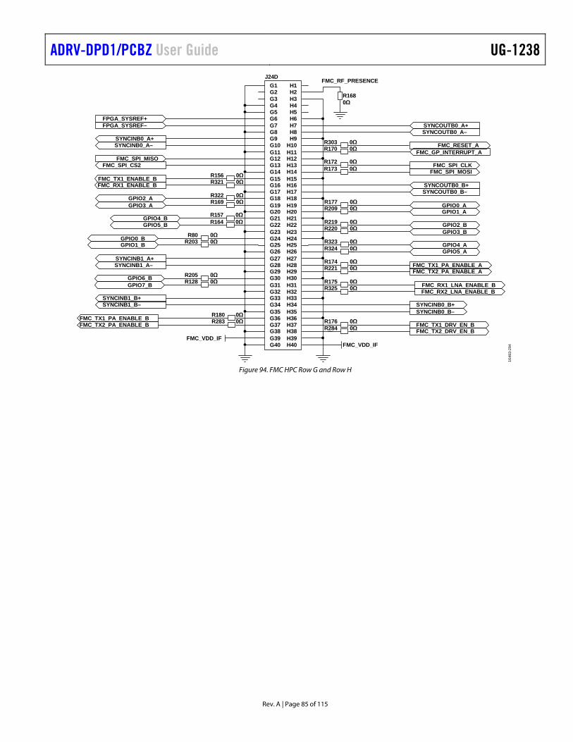
ADRV-DPD1/PCBZ User Guide UG-1238
Rev. A | Page 85 of 115
G1G2G3G4G5
G10G11G12G13G14G15G16G17G18G19G20G21G22G23G24G25G26
H1
H10H11H12H13H14H15H16H17H18H19H20H21H22H23H24H25
G27G28G29G30
H26H27H28H29H30
G31G32G33G34G35G36G37G38G39G40
H31H32H33H34H35H36H37H38H39H40
G6G7G8G9
H2H3H4H5H6H7H8H9
J24D
SYNCINB0_B–SYNCINB0_B+
SYNCINB1_B+SYNCINB1_B–
SYNCOUTB0_A+SYNCOUTB0_A–
FMC_SPI_CLKFMC_SPI_MOSI
FMC_RESET_AFMC_GP_INTERRUPT_A
SYNCINB0_A+SYNCINB0_A–
SYNCINB1_A–SYNCINB1_A+
FMC_SPI_MISO
FMC_TX1_ENABLE_B
FMC_RX2_LNA_ENABLE_B
FMC_TX1_PA_ENABLE_A
FMC_TX1_PA_ENABLE_B
SYNCOUTB0_B+SYNCOUTB0_B–
FMC_RX1_ENABLE_B R321 0Ω
R325 0Ω FMC_RX1_LNA_ENABLE_B
FMC_TX1_DRV_EN_B
FMC_SPI_CS2
FPGA_SYSREF+FPGA_SYSREF–
R303 0ΩR170 0Ω
R172 0ΩR173 0Ω
R174 0Ω
R175 0Ω
R176 0ΩR180 0Ω
FMC_TX2_PA_ENABLE_AR221 0Ω
FMC_TX2_DRV_EN_BR284 0Ω
R156 0Ω
FMC_TX2_PA_ENABLE_B R283 0Ω
R1680Ω
FMC_RF_PRESENCE
FMC_VDD_IFFMC_VDD_IF
R164 0ΩGPIO4_B R157 0Ω
GPIO5_B
GPIO4_AGPIO5_A
R323 0ΩR324 0Ω
GPIO0_B R80 0Ω
GPIO1_B R203 0Ω
GPIO6_B R205 0Ω
GPIO7_B R128 0Ω
GPIO0_AR177 0Ω
GPIO1_AR209 0ΩR169 0ΩGPIO2_A R322 0Ω
GPIO3_A
GPIO2_BR219 0Ω
GPIO3_BR220 0Ω
1649
3-29
4
Figure 94. FMC HPC Row G and Row H

UG-1238 ADRV-DPD1/PCBZ User Guide
Rev. A | Page 86 of 115
J1 K1J2J3J4J5J6J7J8J9J10J11J12J13J14J15J16J17J18J19J20J21J22J23J24J25J26J27J28J29J30J31J32J33J34J35J36J37J38J39J40
K2K3K4K5K6K7K8K9
K10K11K12K13K14K15K16K17K18K19K20K21K22K23K24K25K26K27K28K29K30K31K32K33K34K35K36K37K38K39K40
J24E
3P3V
FMC_RF_PRESENCE_B
FMC_GP_INTERRUPT_B
FMC_RF_PRESENCE_AFMC_TDD1_SWITCH_BFMC_TDD2_SWITCH_B
R1531kΩPG_M2C
FMC_RESET_BR166 0ΩR165 0Ω
E1 F1F2F3F4F5F6F7F8F9
F10F11F12F13F14F15F16F17F18F19F20F21F22F23F24F25F26F27F28F29F30F31F32F33F34F35F36F37F38F39F40
E2E3E4E5E6E7E8E9E10E11E12E13E14E15E16E17E18E19E20E21E22E23E24E25E26E27E28E29E30E31E32E33E34E35E36E37E38E39E40
J24C
FMC_VDD_IF
R304DNF
R313DNF
VDD_IFR319
0Ω
TP9
FMC_VDD_IF
FMC_VDD_IFFMC_VDD_IF
C11947μF
GPIO9_B R261 0Ω
GPIO17_A R199 0ΩGPIO16_A R371 0ΩGPIO8_AR277 0ΩGPIO10_A R182 0Ω
GPIO12_A R317 0ΩGPIO13_A R282 0Ω
R88 0Ω GPIO8_B
GPIO9_AR278 0ΩGPIO11_A R191 0Ω
GPIO14_AR201 0ΩGPIO15_AR279 0Ω
GPIO10_B R262 0Ω
GPIO11_BR202 0ΩGPIO12_BR280 0ΩGPIO14_B R200 0ΩGPIO13_B R372 0Ω
R218 0Ω GPIO15_B
GPIO16_BR207 0ΩGPIO17_BR281 0Ω
GPIO18_B R263 0Ω
SIGNAL PINS IN E, F, J, AND K ARE NOT CONNECTEDON THE EVAL-TPG-ZYNQ3, ONLY POWER PINS.SEE EVAL-TPG-ZYNQ3 DATA SHEET FOR MORE INFORMATION
1649
3-29
5
Figure 95. FMC HPC Row E, Row F, Row J, and Row K, Not Connected on EVAL-TPG-ZYNQ3 (Except for Power Connections)

ADRV-DPD1/PCBZ User Guide UG-1238
Rev. A | Page 87 of 115
C01C02C03C04C05C06C07C08C09C10C11C12C13C14C15C16C17C18C19C20C21C22C23C24C25C26
D01D02D03D04D05D06D07D08D09D10D11D12D13D14D15D16D17D18D19D20D21D22D23D24D25
C27C28C29C30
D26D27D28D29D30
C31C32C33C34C35C36C37C38C39C40
D31D32D33D34D35D36D37D38D39D40
J21AG01G02G03G04G05G06G07G08G09G10G11G12G13G14G15G16G17G18G19G20G21G22G23G24G25G26
H01H02H03H04H05H06H07H08H09H10H11H12H13H14H15H16H17H18H19H20H21H22H23H24H25
G27G28G29G30
H26H27H28H29H30
G31G32G33G34G35G36G37G38G39G40
H31H32H33H34H35H36H37H38H39H40
J21B
DUMMY CONNECTORTO EASE CONNECTION TO EVAL-TPG-ZYNQ3
1649
3-29
6
Figure 96. FMC LPC Dummy Connector
H25
STANDOFF
H1
SCREW
H2
SCREW
H3
SCREW
H4
SCREW
H5
SCREW
H6
SCREW
H7
SCREW
H8
SCREW
H9
WASHERLOCK
WASHERLOCK
WASHERLOCK
WASHERLOCK
WASHERLOCK
WASHERLOCK
WASHERLOCK
WASHERLOCK
H10 H11 H12 H13 H14 H15 H16
H17
WASHER
H18
WASHER
H19
WASHER
H20
WASHER
H21
WASHER
H22
WASHER
H23
WASHER
H24
WASHER
H26
STANDOFF
H27
STANDOFF
H28
STANDOFF
H29
STANDOFF
H30
STANDOFF
H31
STANDOFF
H32
STANDOFF
PCBPCB1
PCB-GENERIC
HW13
2505007
HW14
2505007
HW15
2505007
HW16
31322366 1649
3-29
7
Figure 97. Mechanicals

UG-1238 ADRV-DPD1/PCBZ User Guide
Rev. A | Page 88 of 115
RADIO BOARD SCHEMATICS
R10
15kΩ
R15
10kΩ
C90
3300
pF
R23
10kΩ
R26
22kΩ
R29
10.2
kΩ
+1.3
V_D
IG
+1.3
V_A
NG
+3.3
V +1.8
V
+5V
VREG
VREG
C82
1.0μ
F
C81
1.0μ
F
C85
10μF
C92
10μF
C98
10μF
C10
610
μF
R19
22kΩ
C84
0.10
μF
C91
0.10
μF
C96
0.10
μF
C99
0.10
μF
C93
3300
pF
C97
2200
pF
C10
0
2200
pF
C79
C78
47μF
C80
C77
C88
47μF
C87
47μF
C86
47μF
C12
547
μF
C95
47μF
C94
47μF
C10
947
μFR
2710
kΩ
R25
13kΩ
R18
31.6
kΩ
R17
100k
Ω
S11
D1
6
D2
3G
12
G2
5S2
4D
1_P
7
D2_
P8
Q1
DU
AL
N-C
HA
NN
ELM
OSF
ET
f SW
= 1
.2M
Hz
R13
DN
F
R12
DN
F
L36
1.0μ
H
L35
1.0μ
H
C89
47μF
L27
+1.3
V_D
IG
R11
10kΩ
R9
0Ω
R22
10kΩ
C83
100μ
F
+5V
SS =
2m
s
SS =
2m
s
C16
447
μF
+1.3
V_A
NG
R20 0Ω
C16
647
μF
POW
ER S
EQU
ENC
ING
:1.
+1.
3_D
IG (C
H2)
2. +
1.3V
_AN
G (C
H1)
, +1.
8V (C
H4)
3. +
3.3V
(CH
3)
BST
31
PGN
D3
3
PWR
GD
17
CFG
1218
CO
MP2
20
SW2
25
BST
228
PGN
D30
BST
132
SW1
34PV
IN1
38
FB1
41
FB2
19
EN2
21
PVIN
222
SW2
26SW
227
DL2
29
DL1
31
SW1
33PV
IN1
37
EN1
39
SW3
4
PGN
D3
2
PVIN
36
SW3
5
PVIN
47
SW4
8
SW4
9
PGN
D4
10
FB3
46
VREG
45
CFG
3413
EN4
14
VDD
43
SYN
C/M
OD
E44
CO
MP4
15FB
416
CO
MP1
40
RT
42
EPA
D49
PGN
D4
11
BST
412
PVIN
223
PVIN
224
SW1
35
PVIN
136
CO
MP3
47
EN3
48
U3
AD
P505
4
C16
947
μF
C17
047
μF
C73
100μ
F
L48
VREG
R12
7
6.34
kΩ R12
86.
34kΩ L3
8 L39
L29
2.2μ
H
L28
2.2μ
H
R13
510
0kΩ
VREG
L37
1.3_
AN
ALO
G
C17
6
0.10
μF
C17
7
0.10
μF
1.3_
DIG
ITA
L1.
3_D
IGIT
AL
1.3_
DIG
ITA
L
P_G
OO
D_A
NA
LOG
P_G
OO
D_A
NA
LOG
QU
AD
BU
CK
REG
ULA
TOR
47μF
47μF
47μF
1.3_
DIG
ITA
L
1.3_
AN
ALO
G
1.3_
AN
ALO
G
16493-298
Figure 98. ADP5054 Power Supply

ADRV-DPD1/PCBZ User Guide UG-1238
Rev. A | Page 89 of 115
AD9375
1649
3-29
9
Figure 99. AD9375 Power Connections for VDD_IF, +1.8 V, +1.3_DIG, and +1.3_ANG

UG-1238 ADRV-DPD1/PCBZ User Guide
Rev. A | Page 90 of 115
C380.10μF
C1521.0μF
C480.10μF
+1.3V_ANG
C47100μF
C65100μF
C341.0μF C54
1.0μFC571.0μF
C581.0μF
C591.0μF
C621.0μF
+1.3V_ANG
C68100µF
C69100μF
C660.10μF
C670.10µF
L19
C490.10μF
C510.10μF
C451.0μF
C501.0μF
L21
C530.10μF
C521.0μF
L22
L51
L52
L53
C350.10µF
C2150.10μF
C213100μF
C2141.0μF
C2110.10μF
C641.0μF
C630.10μF
C36100μF
C371.0μF
C21210000pF
L66
L71
L70
L67
VCLK_VCO_LDOM1
VDDA_RXRFB1
VSNRX_VCO_LDOC3
VDDA_SNRXVCOC4
VDDA_RXVCOC7
VRX_VCO_LDOC8
VDDA_TXSYNTHG8
VDDA_SNRXSYNTHG7
VDDA_BBE5
VDDA_RXTXF2
VDDA_TXVCOF11
VTX_VCO_LDOF13
VDDA_SERN8
VDDA_DESN9
VDDA_SERP8
JESD_VTT_DESP9
U1E
AD9375
1649
3-30
0
Figure 100. AD9375 Power Connections for +1.3_ANG and Signal Grounds

ADRV-DPD1/PCBZ User Guide UG-1238
Rev. A | Page 91 of 115
VSSAA1
VSSAM2
VSSAM9
VSSAB3
VSSAB4
VSSAH10
VSSAA4
VSSAA7
VSSAA8
VSSAA11
VSSAJ2
VSSAB2
VSSAH9
VSSAB5
VSSAB6
VSSAB9
VSSAB10
VSSAB11
VSSAB12
VSSAC5
VSSAC9
VSSAC10
VSSAL2
VSSAL1
VSSAK2
VSSAK1
VSSAH8
VSSAH6
VSSAH7
VSSAH5
VSSAH4
VSSAH2
VSSAH3
VSSAG12
VSSAG11
VSSAG10
VSSAG5
VSSAG1
VSSAD6
VSSAD7
VSSAD8
VSSAD9
VSSAE6
VSSAE9
VSSAE10
VSSAF3
VSSAF4
VSSAF5
VSSAF6
VSSAF7
VSSAF8
VSSAF9
VSSAA14
VSSAB13
VSSAG13
VSSAG14
VSSAH13
VSSAJ13
VSSAK13
VSSAK14
VSSAL13
VSSAL14
VSSAN2
VSSAN7
VSSAP10
VSSAP2
VSSAP1
VSSAP3
VSSAN14
VSSAF10
VSSDL10
VSSDL7
VSSAG3
U1D
VSSAG2
AD9375
1649
3-30
1
Figure 101. AD9375 Grounding

UG-1238 ADRV-DPD1/PCBZ User Guide
Rev. A | Page 92 of 115
R514.3kΩ
R1100Ω
DEV_CLK_IN–
SPI_MOSISPI_SCLK
SPI_MISOSPI_MYK_CS
GP_INTERRUPT
TEST
RESET
GPIO4
GPIO5
GPIO6GPIO7
GPIO18
GPIO0GPIO1
GPIO2
GPIO3
C230.10μF
C250.10μF
C311000pF
R24.7kΩ
DEV_CLK_IN+
R41kΩ
VDD_IF
TRST
UNCONNECTEDGPIOs ASSIGNEDAS OUTPUTS ANDASSERTED LOW
R64.7kΩ
R874.7kΩ
R924.7kΩ
R1094.7kΩ GPIO_0_PA1_EN
GPIO_1_LNA1_EN
GPIO_2_PA2_EN
GPIO_3_LNA2_EN
GPIO_4_DRV1_ENGPIO_5_DRV2_EN
GPIO10
M10
L12
L11M11
J12
J11
H12
J10
J8
J9
J6
J5
J4
J3
H11
J7
C1
C2
L6L5
K5
K12
K11K10
K9
K8
K7K6
D1
D5
D12
E1
F1
C13
D13
D14
E14
F14
C11
C12
E7E8
C14
D11
AD9375
TMP_SENSE
UNCONNECTEDGPIOs ASSIGNEDAS OUTPUTS ANDASSERTED LOW
GPIO_0GPIO_1
GPIO_2GPIO_3
GPIO_4GPIO_5
GPIO_6GPIO_7
GPIO_8
GPIO_9GPIO_10
GPIO_11GPIO_12
GPIO_13GPIO_14
GPIO_15GPIO_16
GPIO_17GPIO_18
DEV_CLK_IN–
DEV_CLK_IN+
AUXADC_0
AUXADC_1
AUXADC_2
AUXADC_3
SCLK
SDIOSDOCS
RESET
GP_INTERRUPT
TEST
RBIAS
GPIO_3P3_0
GPIO_3P3_2GPIO_3P3_1
GPIO_3P3_3GPIO_3P3_4
GPIO_3P3_5GPIO_3P3_6
GPIO_3P3_7GPIO_3P3_8
GPIO_3P3_9GPIO_3P3_10
GPIO_3P3_11
E13
U1C
TDOTDI
TMS
TCK
1649
3-30
2
Figure 102. AD9375 Connections for GPIO, 3V3 GPIO, AUXDAC, Interrupt, Clock, and SPI Communications
SERDIN1+
SERDIN2–
SERDIN2+
SERDIN3–
SERDIN3+
SYNCOUTB0–
SYNCOUTB0+
SERDIN0+
SERDIN0–
SYSREF_IN–SYSREF_IN+
TX1_ENABLETX2_ENABLE
RX1_ENABLE
RX2_ENABLE
SYNCINB1+SYNCINB1–
SYNCINB0+
SYNCINB0–
SERDOUT3+SERDOUT3–
SERDOUT2+
SERDOUT2–SERDOUT1+
SERDOUT1–
SERDOUT0+SERDOUT0–
K3
AD9375SERDIN3–
1649
3-30
3
Figure 103. AD9375 JESD204B and Receiver and Transmitter Enables

ADRV-DPD1/PCBZ User Guide UG-1238
Rev. A | Page 93 of 115
VOUTVCC
NCSHD
+3.3V
C261.0μF
R10410kΩ
VDD_IF
R10510kΩ
R10610kΩ
R10710kΩ
R10810kΩ
TMP_SENSEGPIO4GPIO5
GPIO6GPIO7
GPIO18
GND 5
U2
TMP3612
43
1649
3-30
4
Figure 104. GPIO Pull-Up and Temperature Sensor
C3100pFC5100pF
C9100pF
C20.5pF
C1100pF
C66.0pF
C106.0pF
C146.0pF
C126.0pF
C70.5pF
L13.9nH
L23.9nH L3
6.2nHC41.0pF
C81.0pF
L46.2nH
ORX2–ORX2+
RX2–RX2+
RX1+RX1–
ORX1+
TX2+
RX_EXTLO–RX_EXTLO+
TX2–SNRXC–
SNRXB–
SNRXA–
SNRXC+
SNRXB+
SNRXA+
ORX1–
TX1+TX1–
TX_EXTLO–TX_EXTLO+
RX1–
RX1+
RX2–
RX2+
U1_TX1–
U1_TX1+
ORX1–
ORX1+
ORX2–
ORX2+
RX_2
RX_2
A10A9
A6A5
D4E4D3E3D2E2
B7B8
E11E12
J14H14
A13A12
H1J1
A3A2
AD9375
1649
3-30
5
Figure 105. AD9375 RF Interface Connections
C142DNF
C145100pF
TX_1–
ORX_1
RX_1
GND GND
C1610μF
+1.8V_TX_BAL
R580Ω
L10
L1310nH
C180.10μF
R75DNF
R86DNF
L4427nH
L4527nH
C1928.2pF
C1948.2pF
UNBALBAL1
NC
BAL2GND/DC
GND
T3
UNBALBAL1
NC
BAL2GND/DC
GND/NC
T2
C200100pF
C201100pF
GND GND
C115.6pF
L1627nH
TX_1+
C196DNF
C1971.0pF
C1174.3pF
R73DNF
R570Ω
C1544.3pF
C209DNF
C210DNF
R240Ω
R340Ω
PLACE CLOSE TO RFIN± OF U15 INPUT PORTS
RX1–RX1+
U1_TX1–
U1_TX1+
ORX1–ORX1+
125
3
46
125
3
46
1649
3-30
6
Figure 106. Rx1 Balanced to Unbalanced Transformer and Tx1 Filtering

UG-1238 ADRV-DPD1/PCBZ User Guide
Rev. A | Page 94 of 115
ORX_2
RX_2
TX_2–
C15010μF
C144100pF
C151DNF
+1.8V_TX_BAL
R620Ω
L1510nH
C200.10μF
R82DNF
R95DNF
L4627nH
L4727nH
C1938.2pF
C1958.2pF
UNBAL
BAL1
NC
BAL2
GND/DC
GND
T6
UNBAL
BAL1NC
BAL2
GND/DCGND/NC
T5
C198100pF
C199100pF
C135.6pF
L1727nH
TX_2+
C204DNF
C2051.0pF
R84DNF
R640Ω
C2224.3pF
C2234.3pF
C103DNF
C104DNF
R390Ω
R740Ω
PLACE CLOSE TO RFIN± OF U7 INPUT PORTS
RX2+RX2–
ORX2–ORX2+
U1_TX2+U1_TX2–
L11
346
1
25
346
12
5
1649
3-30
7
Figure 107. Rx2 Balanced to Unbalanced Transformer and Tx2 Filtering

ADRV-DPD1/PCBZ User Guide UG-1238
Rev. A | Page 95 of 115
Ω
ΩΩ
ΩPA
1_R
FOU
T
16493-308
Figure 108. ADL5335 and SKY66297 Connections

UG-1238 ADRV-DPD1/PCBZ User Guide
Rev. A | Page 96 of 115
INPUT1
GND 5
DIRECT 2
ISO 3COUPLED4
U5
DIRECTIONALCOUPLER
R5049.9Ω
J4
ANT2
RX1
GND 4
TX3 U6
DUPLEXER
R46
105ΩR5178.7Ω
R5378.7Ω
ORX_1
R28DNF
R30DNF
BYPASS
C162
8.2pF
R98DNF
R97DNF
13dB PAD
GND 3
IN6
GND 2OUT 1
GND4GND5
U4
ISOLATOR
R1370Ω
R136
DNF
R138
DNF
C190
8.2pFI/O 1
GND4O/I3
GND 2
U20
LOW PASS FILTER
BYPASSR3
DNF
L84DNF
PA1_RFOUT
ANT_RX1
1649
3-30
9
Figure 109. Tx1 and Rx1 Antenna and ORX_1 Connection
IN1
GN
D2
GN
D3
GN
D5
OUT 4
U21
BULK ACOUSTICWAVE RF UPLINK FILTER
FOR LTE BAND 7
R59
12Ω
R63430Ω
R61430Ω
RX_1
C1168.2pF
L636nH
+5V_LNA_MAIN
R558.2kΩ
R54
0Ω
C119100pF
L7
1.0nHL8
30nH
LNA1_EN
BYPASS
6dB PAD
+5V_LNA_MAIN+5V
C720.10μF
L33
N/C1
RFIN2
VBIAS3
N/C4 N/C 5ENABLE 6
N/C 8
RFOUT 7
GND9
U13
LOW NOISEAMPLIFIER
L4224nH
C7010μF C112
3300pFC1130.10μF
1 3
2
D2CLA4606-085LF
L57
C183
8.2pF
C1738.2pF C182
8.2pF
C115
8.2pF
C114100pF
C118100pF
R31
DNF
L548.2nH
L584.7nH
R21
0Ω
R14
0Ω
L85
2.7nH
C2171.3pF
C2161.3pF
ANT_RX1 LNA2_OUT
LNA2_OUT
1649
3-31
0
Figure 110. Rx1 SKY67159 Low Noise Amplifier

ADRV-DPD1/PCBZ User Guide UG-1238
Rev. A | Page 97 of 115
C12
133
00pF
R36
0Ω
R35
0Ω
R41
18Ω
R60
294Ω
R44
294Ω
PA2_
EN
TX_2
–
3dB
PA
DC
127
8.2p
F
+5V
C13
347
μF
L41
C15
747
μF
+5V_
PA_D
IV+5V_
PA_D
IV+5
V_PA
_DIV
+5V_
PA_D
IV
+5V_
PA_D
IV
C13
41.
0μF
C12
033
00pF
C13
533
00pF
+5V_
DR
V_D
IV
L60
C18
710
0pF
C18
610
0pF
L59
C13
010
0pF
C18
510
0pF
C18
410
0pF
GN
D1
RFI
N2
GN
D3
GN
D4
GND 7
GND 8RFO
UT
9G
ND
10
GND13VCC214GND15
VCC116 VBIAS 5
PAEN 6
VCC
312
GN
D11
GN
D17
U14
SKY6
6297
-11
TX_2
+
DR
V2_E
N
SPI_
SCLK
SPI_
MO
SI
SPI_
DR
V2_C
S
L75
DN
FL7
6D
NF
C20
610
0pF
+5V_
DR
V_D
IV
SDIO
14R
FIN
+3
FA12
SCLK
15
CS
16
RFI
N–
2
ENBL11
VPOS11
VPOS24
VPOS313
GND4 8
GND1 5
RFO
UT
10
GND2 6
GND3 7
GND5 9
EP17
U7
AD
L533
5
R14
60Ω
R14
4
0Ω
C20
210
0pF
C17
50.
10μF
+5V_
DR
V_D
IV R14
3
0Ω
C17
210
0pF
C17
10.
10μF
+5V_
DR
V_D
IV R12
6
0Ω
C12
133
00pF
L81
C18
510
0pF
+5V
L80
C16
710
μF
C20
30.
10μF
C22
1
8.2p
F
PA2_
RFO
UT
16493-311
Figure 111. Tx2 ADL5335 and SKY66297 Connections

UG-1238 ADRV-DPD1/PCBZ User Guide
Rev. A | Page 98 of 115
INPUT1
GND 5
DIRECT 2
ISO 3COUPLED4
U9
DIRECTIONALCOUPLER
R6549.9Ω
J3
ANT2
RX
1
GND 4
TX3 U11
DUPLEXER
R66
105ΩR6778.7Ω
R6878.7Ω
ORX_2
R37DNF
R38DNF
BYPASS
C163
8.2pF
R101DNF
R100DNF
13dB PAD
GND 3
IN6
GND 2OUT 1
GND4GND5
U8
ISOLATOR
R1400Ω
R139
DNF
R141
DNF
C191
8.2pFI/O 1
GND4O/I3
GND 2
U22
LOW PASS FILTER
BYPASSR16
DNF
L86DNF
PA2_RFOUT
ANT_RX2 1649
3-31
2
Figure 112. Tx2 and Rx2 Antenna and ORX_2 Connection
IN1
GN
DG
ND
GN
D2 3 5
OUT 4
U16
BULK ACOUSTICWAVE UPLINK FILTER
FOR LTE BAND 7
R78
12Ω
R83430Ω
R81430Ω
RX_2
C1408.2pF
L3036nH
+5V_LNA_DIV
R708.2kΩ
R69
0Ω
C149100pF
L31
1.0nHL32
30nH
LNA2_EN
BYPASS
6dB PAD
+5V_LNA_DIV+5V
C760.10μF
L34
N/C1
RFIN2
VBIAS3
N/C4 N/C 5ENABLE 6
N/C 8
RFOUT 7
GND9
U12
LOW NOISEAMPLIFIER
L4324nH
C7410μF C136
3300pFC1380.10μF
1 3
2
D3CLA4606-085LF
L61
C189
8.2pF
C1748.2pF C188
8.2pF
C146
8.2pF
C137100pF
C148100pF
R71
DNF
L628.2nH
L634.7nH
R33
0Ω
R32
0Ω
L87
2.7nH
C2191.3pF
C2181.3pF
ANT_RX2 LNA2_OUT
LNA2_OUT
1649
3-31
3
Figure 113. Rx2 Low Noise Amplifier

ADRV-DPD1/PCBZ User Guide UG-1238
Rev. A | Page 99 of 115
53
8
55
12
57
16
59
20
61
24
63
22
28
13
65
26
32
15
67
30
36
17
69
34
40
71
41
78
19
38
21
4239
23
74
46
37
25
70
50
35
27
66
33
62
31
54
29
58
44
73
48
75
52
77
56
79
60
81
64
1 23
65
107
14
9
18
11
4
5149
94
47
90
45
86
43
82
98
91
80
89
76
87
72
85
68
83
99
9697
92
95
88
93
84
100
J1
SERDOUT1–SERDOUT1+
REMOTE +5V SENSE ON PA PIN 100
SERDOUT0+SERDOUT0–
GPIO0
SERDOUT2+SERDOUT2-
SERDOUT3+SERDOUT3-
SERDIN1–SERDIN1+
SYNCOUTB0–SYNCOUTB0+
SERDIN3+SERDIN3-
SERDIN0+SERDIN0–
SERDIN2–SERDIN2+
SYNCINB1+SYNCINB1–
SYNCINB0+SYNCINB0–
SYSREF_IN–SYSREF_IN+
DEV_CLK_IN–DEV_CLK_IN+
TX1_RADIO_EN
GPIO4
RX1_RADIO_EN
GP_INTERRUPTRESET
GPIO1GPIO2GPIO3
VDD_IF
+5V
GPIO5GPIO6GPIO7GPIO18TEST
C147 0.10μFC139 0.10μF
C132 0.10μFC108 0.10μF
C19 0.10μF
C75 0.10μF
C17 0.10μF
C71 0.10μF
TRSTTDOTDITMSTCK
PRESENCE RF
SPI_DRV2_CSSPI_DRV1_CS
SPI_MOSISPI_SCLK
SPI_MISO
SPI_MYK_CS
+5V
GPIO10
TX_DRV1_ENTX_DRV2_EN
RX_LNA1_ENRX_LNA2_EN
TX_PA1_ENTX_PA2_EN
EEPROM_WPSPI_EEPROM_CS
+5V
1649
3-31
4
Figure 114. 100-Way Connector

UG-1238 ADRV-DPD1/PCBZ User Guide
Rev. A | Page 100 of 115
PA1_EN
PA2_EN
LNA1_EN
LNA2_EN
R40
2.2kΩ
GPIO_1_LNA1_EN
GPIO_3_LNA2_EN
GPIO_0_PA1_EN
R4710kΩ
R112100kΩ
R7610kΩ
R124100kΩ
R93
2.2kΩ
R121
2.2kΩ
1A1
GND2
2A3
1Y 6
VCC 5
2Y 4
U19
1A1
GND2
2A3
1Y 6
VCC 5
2Y 4
U17 VDD_IF
VDD_IF
R5210kΩ
R5610kΩ
R11310kΩ
R11610kΩ
R94100kΩ
R117100kΩ
+5V
GPIO_2_PA2_ENR72
2.2kΩ
+5V
INVERTERWITH OPEN-DRAIN
OUTPUTS
C151.0μF
C1591.0μF
DRV1_EN
DRV2_EN
R77
8.2kΩGPIO_4_DRV1_EN
R8510kΩ
R9110kΩ
R8810kΩ
R8910kΩ
GPIO_5_DRV2_ENR90
8.2kΩ
BUFFERWITH OPEN-DRAIN
OUTPUTS
BUFFERWITH OPEN-DRAIN
OUTPUTS
C1581.0μF
1A1
GND2
2A3
1Y 6
VCC 5
2Y 4
U18
CS1
SO2
WP3
GND4 SI 5SCL 6
HOLD 7VCC 8
U23
VDD_IF
C1600.10μF
SPI_CSB2SPI_CSB1
R1474.7kΩ
R1484.7kΩ
VDD_IF
R1314.7kΩ
VDD_IF
R13310kΩ R132
10kΩ
VDD_IFTX_DRV1_EN
TX_DRV2_EN
SPI_EEPROM_CS
EEPROM_WP
TX_PA1_EN
TX_PA2_EN
RX_LNA1_EN
RX_LNA2_EN
SPI_SCLKSPI_MOSI
SPI_MISO SPI_CSB2SPI_CSB1
1649
3-31
5
Figure 115. Amplifier Enable Buffers and SPI EEPROM

ADRV-DPD1/PCBZ User Guide UG-1238
Rev. A | Page 101 of 115
SH131082267
SH231082268PCB
PCB1
31282247
SH331082269
HW8
SCREW
HW5
SCREW
HW6
SCREW
HW7
SCREW
HW9
SCREW
HW10
SCREW
HW11
SCREW
HW12
WASHERPLAIN
HW13
WASHERPLAIN
HW14
WASHERPLAIN
HW17
WASHERLOCK
HW15
WASHERLOCK
HW16
WASHERLOCK
HW18
HEATSINK,MACHINING
HW19
HEATSINK,INTERFACE
HW20
THERMALCOMPOUND
HW21
GAP PAD
HW22
GAP PAD
HW23
GAP PAD
HW24
EMCGASKET
PCBHW1
567-581
PCBHW2
567-581
PCBHW3
567-581
PCBHW4
567-581
HW25
M0538-3-AL
HW26
M0538-3-AL
HW27
M0538-3-AL
HW27
M0538-3-AL
1649
3-31
6
Figure 116. Mechanicals

UG-1238 ADRV-DPD1/PCBZ User Guide
Rev. A | Page 102 of 115
INTERPOSER BOARD PCB LAYERS The eight layers of etched copper in the interposer board are shown in Figure 117 to Figure 124. Grey indicates a plated through hole to the adjacent layer(s). The board layers are made from Isola FR408HR FR4 with a copper foil. The boards make use of blind vias to connect between layers.
1649
3-31
7
Figure 117. Layer 1 (Top)

ADRV-DPD1/PCBZ User Guide UG-1238
Rev. A | Page 103 of 115
1649
3-31
8
Figure 118. Layer 2

UG-1238 ADRV-DPD1/PCBZ User Guide
Rev. A | Page 104 of 115
1649
3-31
9
Figure 119. Layer 3

ADRV-DPD1/PCBZ User Guide UG-1238
Rev. A | Page 105 of 115
1649
3-32
0
Figure 120. Layer 4

UG-1238 ADRV-DPD1/PCBZ User Guide
Rev. A | Page 106 of 115
1649
3-32
1
Figure 121. Layer 5

ADRV-DPD1/PCBZ User Guide UG-1238
Rev. A | Page 107 of 115
1649
3-32
2
Figure 122. Layer 6

UG-1238 ADRV-DPD1/PCBZ User Guide
Rev. A | Page 108 of 115
1649
3-32
3
Figure 123. Layer 7

ADRV-DPD1/PCBZ User Guide UG-1238
Rev. A | Page 109 of 115
1649
3-32
4
Figure 124. Layer 8 (Bottom)

UG-1238 ADRV-DPD1/PCBZ User Guide
Rev. A | Page 110 of 115
RADIO BOARD PCB LAYERS The eight layers of etched copper in the radio board are shown in Figure 125 to Figure 132. Grey indicates a plated through hole to the adjacent layer(s). The board layers are made from Isola FR408HR FR4 with a copper foil. The boards make use of blind vias to connect between layers.
1649
3-32
5
Figure 125. Layer 1 (Bottom, 100-Pin Connector Side)
1649
3-32
6
Figure 126. Layer 2

ADRV-DPD1/PCBZ User Guide UG-1238
Rev. A | Page 111 of 115
1649
3-32
7
Figure 127. Layer 3
1649
3-32
8
Figure 128. Layer 4

UG-1238 ADRV-DPD1/PCBZ User Guide
Rev. A | Page 112 of 115
1649
3-32
9
Figure 129. Layer 5
1649
3-33
0
Figure 130. Layer 6
ADRV-DPD1/PCBZ User Guide UG-1238
Rev. A | Page 113 of 115
1649
3-33
1
Figure 131. Layer 7
1649
3-33
2
Figure 132. Layer 8 (Top, Antenna Connector Side)

UG-1238 ADRV-DPD1/PCBZ User Guide
Rev. A | Page 114 of 115
INTERPOSER BOARD CONNECTORS AND LEDS
16493-042
Figure 133. ADRV-INTERPOS1/PCBZ Board Layout Schematic

ADRV-DPD1/PCBZ User Guide UG-1238
Rev. A | Page 115 of 115
NOTES
ESD Caution ESD (electrostatic discharge) sensitive device. Charged devices and circuit boards can discharge without detection. Although this product features patented or proprietary protection circuitry, damage may occur on devices subjected to high energy ESD. Therefore, proper ESD precautions should be taken to avoid performance degradation or loss of functionality.
Legal Terms and Conditions By using the evaluation board discussed herein (together with any tools, components documentation or support materials, the “Evaluation Board”), you are agreeing to be bound by the terms and conditions set forth below (“Agreement”) unless you have purchased the Evaluation Board, in which case the Analog Devices Standard Terms and Conditions of Sale shall govern. Do not use the Evaluation Board until you have read and agreed to the Agreement. Your use of the Evaluation Board shall signify your acceptance of the Agreement. This Agreement is made by and between you (“Customer”) and Analog Devices, Inc. (“ADI”), with its principal place of business at One Technology Way, Norwood, MA 02062, USA. Subject to the terms and conditions of the Agreement, ADI hereby grants to Customer a free, limited, personal, temporary, non-exclusive, non-sublicensable, non-transferable license to use the Evaluation Board FOR EVALUATION PURPOSES ONLY. Customer understands and agrees that the Evaluation Board is provided for the sole and exclusive purpose referenced above, and agrees not to use the Evaluation Board for any other purpose. Furthermore, the license granted is expressly made subject to the following additional limitations: Customer shall not (i) rent, lease, display, sell, transfer, assign, sublicense, or distribute the Evaluation Board; and (ii) permit any Third Party to access the Evaluation Board. As used herein, the term “Third Party” includes any entity other than ADI, Customer, their employees, affiliates and in-house consultants. The Evaluation Board is NOT sold to Customer; all rights not expressly granted herein, including ownership of the Evaluation Board, are reserved by ADI. CONFIDENTIALITY. This Agreement and the Evaluation Board shall all be considered the confidential and proprietary information of ADI. Customer may not disclose or transfer any portion of the Evaluation Board to any other party for any reason. Upon discontinuation of use of the Evaluation Board or termination of this Agreement, Customer agrees to promptly return the Evaluation Board to ADI. ADDITIONAL RESTRICTIONS. Customer may not disassemble, decompile or reverse engineer chips on the Evaluation Board. Customer shall inform ADI of any occurred damages or any modifications or alterations it makes to the Evaluation Board, including but not limited to soldering or any other activity that affects the material content of the Evaluation Board. Modifications to the Evaluation Board must comply with applicable law, including but not limited to the RoHS Directive. TERMINATION. ADI may terminate this Agreement at any time upon giving written notice to Customer. Customer agrees to return to ADI the Evaluation Board at that time. LIMITATION OF LIABILITY. THE EVALUATION BOARD PROVIDED HEREUNDER IS PROVIDED “AS IS” AND ADI MAKES NO WARRANTIES OR REPRESENTATIONS OF ANY KIND WITH RESPECT TO IT. ADI SPECIFICALLY DISCLAIMS ANY REPRESENTATIONS, ENDORSEMENTS, GUARANTEES, OR WARRANTIES, EXPRESS OR IMPLIED, RELATED TO THE EVALUATION BOARD INCLUDING, BUT NOT LIMITED TO, THE IMPLIED WARRANTY OF MERCHANTABILITY, TITLE, FITNESS FOR A PARTICULAR PURPOSE OR NONINFRINGEMENT OF INTELLECTUAL PROPERTY RIGHTS. IN NO EVENT WILL ADI AND ITS LICENSORS BE LIABLE FOR ANY INCIDENTAL, SPECIAL, INDIRECT, OR CONSEQUENTIAL DAMAGES RESULTING FROM CUSTOMER’S POSSESSION OR USE OF THE EVALUATION BOARD, INCLUDING BUT NOT LIMITED TO LOST PROFITS, DELAY COSTS, LABOR COSTS OR LOSS OF GOODWILL. ADI’S TOTAL LIABILITY FROM ANY AND ALL CAUSES SHALL BE LIMITED TO THE AMOUNT OF ONE HUNDRED US DOLLARS ($100.00). EXPORT. Customer agrees that it will not directly or indirectly export the Evaluation Board to another country, and that it will comply with all applicable United States federal laws and regulations relating to exports. GOVERNING LAW. This Agreement shall be governed by and construed in accordance with the substantive laws of the Commonwealth of Massachusetts (excluding conflict of law rules). Any legal action regarding this Agreement will be heard in the state or federal courts having jurisdiction in Suffolk County, Massachusetts, and Customer hereby submits to the personal jurisdiction and venue of such courts. The United Nations Convention on Contracts for the International Sale of Goods shall not apply to this Agreement and is expressly disclaimed.
©2018 Analog Devices, Inc. All rights reserved. Trademarks and registered trademarks are the property of their respective owners. UG16493-0-7/18(A)