adp3196 6-bit programmable 2- to 4-phase synchronous buck
TRANSCRIPT
6-Bit Programmable 2- to 4-Phase Synchronous Buck Controller
ADP3196
Rev. 0 Information furnished by Analog Devices is believed to be accurate and reliable. However, no responsibility is assumed by Analog Devices for its use, nor for any infringements of patents or other rights of third parties that may result from its use. Specifications subject to change without notice. No license is granted by implication or otherwise under any patent or patent rights of Analog Devices. Trademarks and registered trademarks are the property of their respective owners.
One Technology Way, P.O. Box 9106, Norwood, MA 02062-9106, U.S.A.Tel: 781.329.4700 www.analog.com Fax: 781.461.3113 ©2006 Analog Devices, Inc. All rights reserved.
FEATURES
Selectable 2-, 3-, or 4-phase operation at up to 1 MHz per phase
±10 mV worst-case differential sensing error over temperature
Logic-level PWM outputs for interface to external high power drivers
Enhanced PWM flex mode for excellent load transient performance
Active current balancing between all output phases Built-in power-good/crowbar blanking supports on-the-fly
VID code changes Digitally programmable 0.3750 V to 1.55 V output Programmable short-circuit protection with programmable
latch-off delay
APPLICATIONS Desktop PC power supplies for next generation
AMD processors VRM modules
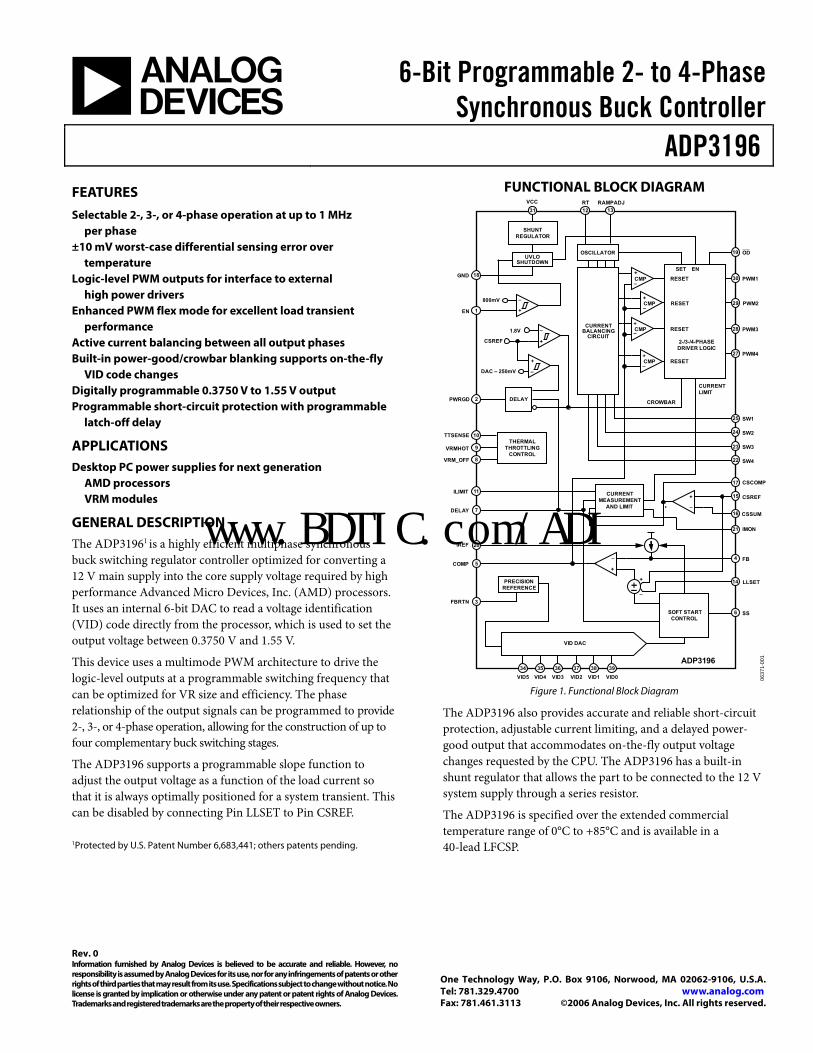
GENERAL DESCRIPTION The ADP31961 is a highly efficient multiphase synchronous buck switching regulator controller optimized for converting a 12 V main supply into the core supply voltage required by high performance Advanced Micro Devices, Inc. (AMD) processors. It uses an internal 6-bit DAC to read a voltage identification (VID) code directly from the processor, which is used to set the output voltage between 0.3750 V and 1.55 V.
This device uses a multimode PWM architecture to drive the logic-level outputs at a programmable switching frequency that can be optimized for VR size and efficiency. The phase relationship of the output signals can be programmed to provide 2-, 3-, or 4-phase operation, allowing for the construction of up to four complementary buck switching stages.
The ADP3196 supports a programmable slope function to adjust the output voltage as a function of the load current so that it is always optimally positioned for a system transient. This can be disabled by connecting Pin LLSET to Pin CSREF.
1Protected by U.S. Patent Number 6,683,441; others patents pending.
FUNCTIONAL BLOCK DIAGRAM VCC
PRECISIONREFERENCE
DELAY
–
+
GND
ADP3196
EN
DELAY
ILIMIT
PWRGD
RAMPADJRT
PWM2
PWM3
PWM4
SW3
SW2
SW1
CSREF
CSCOMP
SW4
CSSUM
FB
PWM1
VID5 VID4 VID3 VID2 VID0VID1
COMP
FBRTN
VID DAC
–
+
800mV –
+
CSREF
1.8V
CURRENTMEASUREMENT
AND LIMIT
CROWBAR
CURRENTLIMIT
+
–CMP
+
–CMP
+
–CMP
+
–
+
–CMPCURRENT
BALANCINGCIRCUIT
2-/3-/4-PHASEDRIVER LOGIC
ENSET
RESET
RESET
RESET
RESET
OD
SS
–
+
IREF
THERMALTHROTTLING
CONTROL
TTSENSE
VRMHOT
VRM_OFF
LLSET
UVLOSHUTDOWN
SHUNTREGULATOR
IMON
–
+
DAC – 250mV
OSCILLATOR
SOFT STARTCONTROL
131231
18
1
2
10
9
11
8
7
5
20
3
393534 3836 37
6
23
16
15
29
28
27
19
17
4
24
22
25
30
14
21
0637
1-00
1
Figure 1. Functional Block Diagram
The ADP3196 also provides accurate and reliable short-circuit protection, adjustable current limiting, and a delayed power-good output that accommodates on-the-fly output voltage changes requested by the CPU. The ADP3196 has a built-in shunt regulator that allows the part to be connected to the 12 V system supply through a series resistor.
The ADP3196 is specified over the extended commercial temperature range of 0°C to +85°C and is available in a 40-lead LFCSP.
www.BDTIC.com/ADI
ADP3196
Rev. 0 | Page 2 of 20
TABLE OF CONTENTS Features .............................................................................................. 1 Applications....................................................................................... 1 General Description ......................................................................... 1 Functional Block Diagram .............................................................. 1 Table of Contents .............................................................................. 2 Revision History ............................................................................... 2 Specifications..................................................................................... 3 Test Circuits....................................................................................... 5 Absolute Maximum Ratings............................................................ 6
ESD Caution.................................................................................. 6 Pin Configuration and Function Description .............................. 7 Typical Performance Characteristics ............................................. 9 Theory of Operation ...................................................................... 10
Start-Up Sequence...................................................................... 10 Phase Detection Sequence......................................................... 10 Master Clock Frequency............................................................ 11 Output Voltage Differential Sensing ........................................ 11
Output Current Sensing ............................................................ 11 Active Impedance Control Mode............................................. 11 Current Control Mode and Thermal Balance ........................ 11 Voltage Control Mode ............................................................... 12 Current Reference ...................................................................... 12 Enhanced PWM Mode.............................................................. 12 Delay Timer................................................................................. 12 Soft Start ...................................................................................... 12 Current Limit, Short-Circuit, and Latch-Off Protection ...... 13 Dynamic VID ............................................................................. 14 Power-Good Monitoring........................................................... 14 Output Crowbar ......................................................................... 14 Output Enable and UVLO ........................................................ 14 Thermal Monitoring .................................................................. 14 Layout and Component Placement ......................................... 17
Outline Dimensions ....................................................................... 18 Ordering Guide .......................................................................... 18
REVISION HISTORY 10/06—Revision 0: Initial Version
www.BDTIC.com/ADI
ADP3196
Rev. 0 | Page 3 of 20
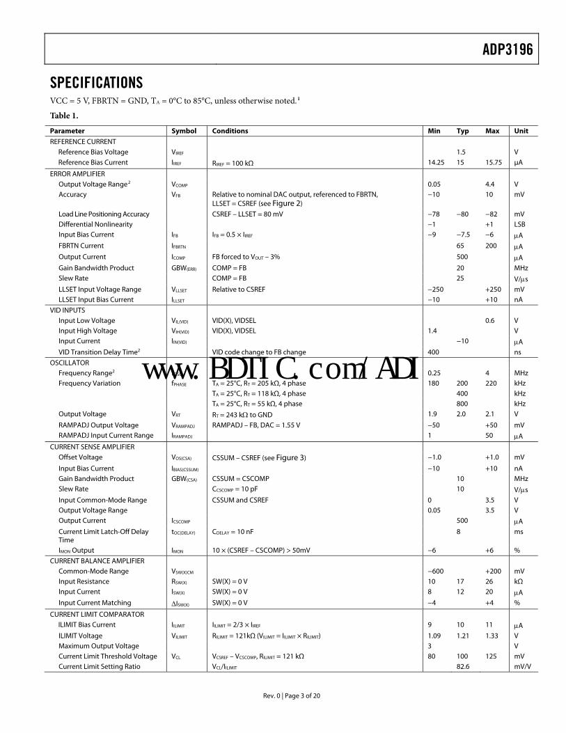
SPECIFICATIONS VCC = 5 V, FBRTN = GND, TA = 0°C to 85°C, unless otherwise noted.1
Table 1.
Parameter Symbol Conditions Min Typ Max Unit
REFERENCE CURRENT Reference Bias Voltage VIREF 1.5 V Reference Bias Current IIREF RIREF = 100 kΩ 14.25 15 15.75 μA
ERROR AMPLIFIER Output Voltage Range2 VCOMP 0.05 4.4 V Accuracy VFB Relative to nominal DAC output, referenced to FBRTN,
LLSET = CSREF (see Figure 2) −10 10 mV
Load Line Positioning Accuracy CSREF – LLSET = 80 mV −78 −80 −82 mV Differential Nonlinearity −1 +1 LSB Input Bias Current IFB IFB = 0.5 × IIREF −9 −7.5 −6 μA FBRTN Current IFBRTN 65 200 μA Output Current ICOMP FB forced to VOUT – 3% 500 μA Gain Bandwidth Product GBW(ERR) COMP = FB 20 MHz Slew Rate COMP = FB 25 V/μs LLSET Input Voltage Range VLLSET Relative to CSREF −250 +250 mV LLSET Input Bias Current ILLSET −10 +10 nA
VID INPUTS Input Low Voltage VIL(VID) VID(X), VIDSEL 0.6 V Input High Voltage VIH(VID) VID(X), VIDSEL 1.4 V Input Current IIN(VID) −10 μA VID Transition Delay Time2 VID code change to FB change 400 ns
OSCILLATOR Frequency Range2 fOSC 0.25 4 MHz Frequency Variation fPHASE TA = 25°C, RT = 205 kΩ, 4 phase 180 200 220 kHz TA = 25°C, RT = 118 kΩ, 4 phase 400 kHz TA = 25°C, RT = 55 kΩ, 4 phase 800 kHz Output Voltage VRT RT = 243 kΩ to GND 1.9 2.0 2.1 V
RAMPADJ Output Voltage VRAMPADJ RAMPADJ – FB, DAC = 1.55 V −50 +50 mV RAMPADJ Input Current Range IRAMPADJ 1 50 μA
CURRENT SENSE AMPLIFIER Offset Voltage VOS(CSA) CSSUM – CSREF (see Figure 3) −1.0 +1.0 mV
Input Bias Current IBIAS(CSSUM) −10 +10 nA Gain Bandwidth Product GBW(CSA) CSSUM = CSCOMP 10 MHz Slew Rate CCSCOMP = 10 pF 10 V/μs Input Common-Mode Range CSSUM and CSREF 0 3.5 V Output Voltage Range 0.05 3.5 V Output Current ICSCOMP 500 μA Current Limit Latch-Off Delay Time
tOC(DELAY) CDELAY = 10 nF 8 ms
IMON Output IMON 10 × (CSREF – CSCOMP) > 50mV −6 +6 %
CURRENT BALANCE AMPLIFIER Common-Mode Range VSW(X)CM −600 +200 mV Input Resistance RSW(X) SW(X) = 0 V 10 17 26 kΩ Input Current ISW(X) SW(X) = 0 V 8 12 20 μA Input Current Matching ΔISW(X) SW(X) = 0 V −4 +4 %
CURRENT LIMIT COMPARATOR ILIMIT Bias Current IILIMIT IILIMIT = 2/3 × IIREF 9 10 11 μA ILIMIT Voltage VILIMIT RILIMIT = 121kΩ (VILIMIT = IILIMIT × RILIMIT) 1.09 1.21 1.33 V Maximum Output Voltage 3 V Current Limit Threshold Voltage VCL VCSREF – VCSCOMP, RILIMIT = 121 kΩ 80 100 125 mV Current Limit Setting Ratio VCL/IILIMIT 82.6 mV/V
www.BDTIC.com/ADI
ADP3196
Rev. 0 | Page 4 of 20
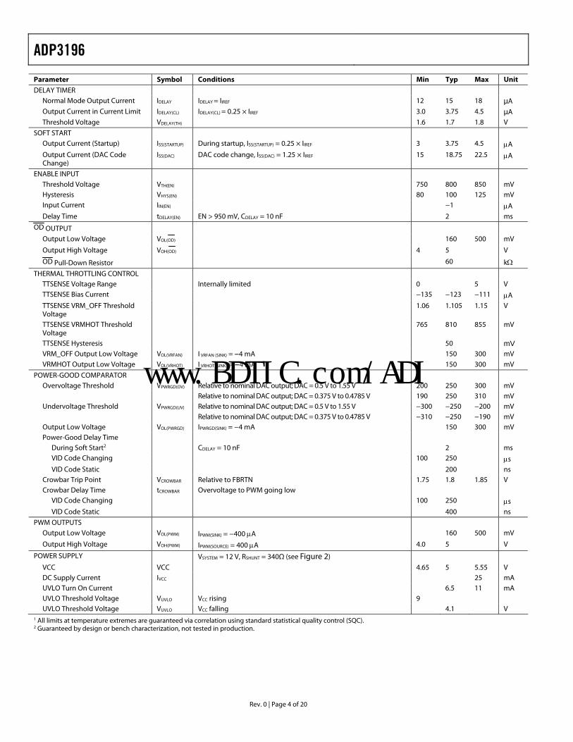
Parameter Symbol Conditions Min Typ Max Unit
DELAY TIMER Normal Mode Output Current IDELAY IDELAY = IIREF 12 15 18 µA Output Current in Current Limit IDELAY(CL) IDELAY(CL) = 0.25 × IIREF 3.0 3.75 4.5 µA Threshold Voltage VDELAY(TH) 1.6 1.7 1.8 V
SOFT START Output Current (Startup) ISS(STARTUP) During startup, ISS(STARTUP) = 0.25 × IIREF 3 3.75 4.5 μA Output Current (DAC Code Change)
ISS(DAC) DAC code change, ISS(DAC) = 1.25 × IIREF 15 18.75 22.5 μA
ENABLE INPUT Threshold Voltage VTH(EN) 750 800 850 mV Hysteresis VHYS(EN) 80 100 125 mV Input Current IIN(EN) −1 μA Delay Time tDELAY(EN) EN > 950 mV, CDELAY = 10 nF 2 ms
OD OUTPUT
Output Low Voltage VOL(OD) 160 500 mV
Output High Voltage VOH(OD) 4 5 V
OD Pull-Down Resistor 60 kΩ
THERMAL THROTTLING CONTROL TTSENSE Voltage Range Internally limited 0 5 V TTSENSE Bias Current −135 −123 −111 μA TTSENSE VRM_OFF Threshold Voltage
1.06 1.105 1.15 V
TTSENSE VRMHOT Threshold Voltage
765 810 855 mV
TTSENSE Hysteresis 50 mV VRM_OFF Output Low Voltage VOL(VRFAN) I VRFAN (SINK) = −4 mA 150 300 mV VRMHOT Output Low Voltage VOL(VRHOT) I VRHOT (SINK) = −4 mA 150 300 mV
POWER-GOOD COMPARATOR Overvoltage Threshold VPWRGD(OV) Relative to nominal DAC output; DAC = 0.5 V to 1.55 V 200 250 300 mV Relative to nominal DAC output; DAC = 0.375 V to 0.4785 V 190 250 310 mV Undervoltage Threshold VPWRGD(UV) Relative to nominal DAC output; DAC = 0.5 V to 1.55 V −300 −250 −200 mV Relative to nominal DAC output; DAC = 0.375 V to 0.4785 V −310 −250 −190 mV Output Low Voltage VOL(PWRGD) IPWRGD(SINK) = −4 mA 150 300 mV Power-Good Delay Time
During Soft Start2 CDELAY = 10 nF 2 ms VID Code Changing 100 250 μs VID Code Static 200 ns
Crowbar Trip Point VCROWBAR Relative to FBRTN 1.75 1.8 1.85 V Crowbar Delay Time tCROWBAR Overvoltage to PWM going low
VID Code Changing 100 250 μs VID Code Static 400 ns
PWM OUTPUTS Output Low Voltage VOL(PWM) IPWM(SINK) = −400 μA 160 500 mV
Output High Voltage VOH(PWM) IPWM(SOURCE) = 400 μA 4.0 5 V
POWER SUPPLY VSYSTEM = 12 V, RSHUNT = 340Ω (see Figure 2)
VCC VCC 4.65 5 5.55 V DC Supply Current IVCC 25 mA UVLO Turn On Current 6.5 11 mA UVLO Threshold Voltage VUVLO VCC rising 9 UVLO Threshold Voltage VUVLO VCC falling 4.1 V
1 All limits at temperature extremes are guaranteed via correlation using standard statistical quality control (SQC). 2 Guaranteed by design or bench characterization, not tested in production.
www.BDTIC.com/ADI
ADP3196
Rev. 0 | Page 5 of 20
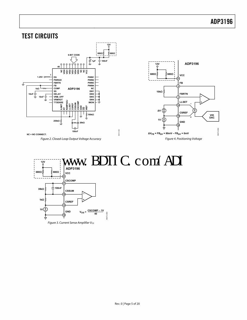
TEST CIRCUITS
ENPWRGDFBRTNFBCOMPSSDELAYVRM_OFFVRMHOTTTSENSE
PWM1PWM2PWM3PWM4
NCSW1SW2SW3SW4
IMON
NC
VID
0VI
D1
VID
2VI
D3
VID
4VI
D5
NC
NC
VCC
ILIM
ITR
TR
AM
PAD
JLL
SET
CSR
EFC
SSU
MC
SCO
MP
GN
DO
DIR
EF
6-BIT CODE
10nF
1µF
10nF
100nF
20kΩ
100kΩ
250kΩ
1kΩ
100nF
ADP3196
40
11.25V
+
680Ω680Ω
12V
NC = NO CONNECT. 0637
1-00
2
Figure 2. Closed-Loop Output Voltage Accuracy
CSSUM
17CSCOMP
16
31VCC
CSREF15
GND18
39kΩ
680Ω 680Ω
100nF
1kΩ
1V
ADP3196
VOS = CSCOMP – 1V40
12V
0637
1-00
3
Figure 3. Current Sense Amplifier VOS
31VCC
10kΩ
ΔV
1V
ADP3196
680Ω 680Ω
12V
ΔVFB = FBΔV = 80mV – FBΔV = 0mV
+
–
4FB
3FBRTN
14LLSET
15CSREF
18GND
VIDDAC
0637
1-00
4
Figure 4. Positioning Voltage
www.BDTIC.com/ADI
ADP3196
Rev. 0 | Page 6 of 20
ABSOLUTE MAXIMUM RATINGS Table 2. Parameter Rating VCC −0.3 V to +6 V FBRTN −0.3 V to +0.3 V PWM3 – PWM4, RAMPADJ −0.3 V to VCC + 0.3 V SW1 – SW4 −5 V to +25 V
<200 ns −10 V to +25 V All Other Inputs and Outputs −0.3 V to VCC + 0.3 V Storage Temperature −65°C to +150°C Operating Ambient Temperature Range 0°C to 85°C Operating Junction Temperature 125°C
Thermal Impedance (θJA) 100°C/W
Lead Temperature Soldering (10 sec) 300°C Infrared (15 sec) 260°C
Stresses above those listed under Absolute Maximum Ratings may cause permanent damage to the device. This is a stress rating only and functional operation of the device at these or any other conditions above those indicated in the operational section of this specification is not implied. Exposure to absolute maximum rating conditions for extended periods may affect device reliability. Absolute maximum ratings apply individually only, not in combination. Unless otherwise specified all other voltages referenced to GND.
ESD CAUTION
www.BDTIC.com/ADI
ADP3196
Rev. 0 | Page 7 of 20
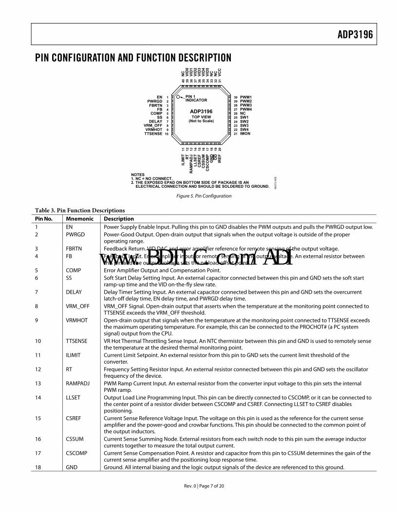
PIN CONFIGURATION AND FUNCTION DESCRIPTION
PIN 1INDICATOR
1EN2PWRGD3FBRTN4FB5COMP6SS7DELAY8VRM_OFF9VRMHOT
10TTSENSE
23 SW324 SW225 SW126 NC27 PWM428 PWM329 PWM230 PWM1
22 SW421 IMON
11IL
IMIT
12R
T13
RA
MPA
DJ
15C
SREF
17C
SCO
MP
16C
SSU
M
18G
ND
19O
D20
IREF
14LL
SET
33N
C34
VID
535
VID
436
VID
337
VID
238
VID
139
VID
040
NC
32N
C31
VCC
TOP VIEW(Not to Scale)
ADP3196
NOTES1. NC = NO CONNECT.2. THE EXPOSED EPAD ON BOTTOM SIDE OF PACKAGE IS AN ELECTRICAL CONNECTION AND SHOULD BE SOLDERED TO GROUND. 06
371-
005
Figure 5. Pin Configuration
Table 3. Pin Function Descriptions Pin No. Mnemonic Description 1 EN Power Supply Enable Input. Pulling this pin to GND disables the PWM outputs and pulls the PWRGD output low. 2 PWRGD Power-Good Output. Open-drain output that signals when the output voltage is outside of the proper
operating range. 3 FBRTN Feedback Return. VID DAC and error amplifier reference for remote sensing of the output voltage. 4 FB Feedback Input. Error amplifier input for remote sensing of the output voltage. An external resistor between
this pin and the output voltage sets the no load offset point. 5 COMP Error Amplifier Output and Compensation Point. 6 SS Soft Start Delay Setting Input. An external capacitor connected between this pin and GND sets the soft start
ramp-up time and the VID on-the-fly slew rate. 7 DELAY Delay Timer Setting Input. An external capacitor connected between this pin and GND sets the overcurrent
latch-off delay time, EN delay time, and PWRGD delay time. 8 VRM_OFF VRM_OFF Signal. Open-drain output that asserts when the temperature at the monitoring point connected to
TTSENSE exceeds the VRM_OFF threshold. 9 VRMHOT Open-drain output that signals when the temperature at the monitoring point connected to TTSENSE exceeds
the maximum operating temperature. For example, this can be connected to the PROCHOT# (a PC system signal) output from the CPU.
10 TTSENSE VR Hot Thermal Throttling Sense Input. An NTC thermistor between this pin and GND is used to remotely sense the temperature at the desired thermal monitoring point.
11 ILIMIT Current Limit Setpoint. An external resistor from this pin to GND sets the current limit threshold of the converter.
12 RT Frequency Setting Resistor Input. An external resistor connected between this pin and GND sets the oscillator frequency of the device.
13 RAMPADJ PWM Ramp Current Input. An external resistor from the converter input voltage to this pin sets the internal PWM ramp.
14 LLSET Output Load Line Programming Input. This pin can be directly connected to CSCOMP, or it can be connected to the center point of a resistor divider between CSCOMP and CSREF. Connecting LLSET to CSREF disables positioning.
15 CSREF Current Sense Reference Voltage Input. The voltage on this pin is used as the reference for the current sense amplifier and the power-good and crowbar functions. This pin should be connected to the common point of the output inductors.
16 CSSUM Current Sense Summing Node. External resistors from each switch node to this pin sum the average inductor currents together to measure the total output current.
17 CSCOMP Current Sense Compensation Point. A resistor and capacitor from this pin to CSSUM determines the gain of the current sense amplifier and the positioning loop response time.
18 GND Ground. All internal biasing and the logic output signals of the device are referenced to this ground.
www.BDTIC.com/ADI
ADP3196
Rev. 0 | Page 8 of 20
Pin No. Mnemonic Description 19 OD Output Disable Logic Output. This pin is actively pulled low when the ADP3196 EN input is low or when VCC is
below its UVLO threshold to signal to the driver IC that the driver high-side and low-side outputs should go low. 20 IREF Current Reference Input. An external resistor from this pin to ground sets the reference current for IFB, IDELAY, ISS,
IILIMIT and ITTSENSE. 21 IMON Analog Output. Represents total load current. 22 to 25 SW4 to SW1 Current Balance Inputs. Inputs for measuring the current level in each phase. The SW pins of unused phases
should be left open. 26, 32, 33, 40
NC No Connection.
27 to 30 PWM4 to PMW1
Logic Level PWM Outputs. Each output is connected to the input of an external MOSFET driver, such as the ADP3120A. Connecting the PWM3 and/or PWM4 outputs to the ADP3196 VCC pin causes that phase to turn off, allowing the ADP3196 to operate as a 2-, 3-, or 4-phase controller.
31 VCC A 340 Ω resistor should be placed between the 12 V system supply and the VCC pin. The internal shunt regulator maintains VCC = 5 V.
34 to 39 VID5 to VID0 Voltage Code DAC Inputs. These six pins are pulled down to GND, providing a logic zero if left open. When in normal operation mode, the DAC output programs the FB regulation voltage from 0.3750 V and 1.55 V (see Table 4).
www.BDTIC.com/ADI
ADP3196
Rev. 0 | Page 9 of 20
TYPICAL PERFORMANCE CHARACTERISTICS
0
800
1600
2400
3200
4000
4800
5600
6400
7200
0 100 200 300 400 500 600 700 800 90006
371-
015
RT (kΩ)
FREQ
UEN
CY
(kH
z)
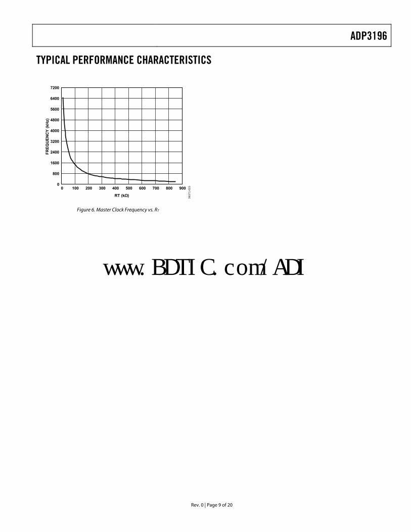
Figure 6. Master Clock Frequency vs. RT
www.BDTIC.com/ADI

ADP3196
Rev. 0 | Page 10 of 20
THEORY OF OPERATION The ADP3196 combines a multimode, fixed frequency PWM control with multiphase logic outputs for use in 2-, 3-, and 4-phase synchronous buck CPU core supply power converters. The internal VID DAC is designed to interface with the AMD 6-bit CPUs.
Multiphase operation is important for producing the high currents and low voltages demanded by today’s microprocessors. Handling the high currents in a single-phase converter places high thermal demands on the components in the system, such as the inductors and MOSFETs.
The multimode control of the ADP3196 ensures a stable, high performance topology for the following:
• Balancing currents and thermals between phases
• High speed response at the lowest possible switching frequency and output decoupling
• Minimizing thermal switching losses by utilizing lower frequency operation
• Tight load line regulation and accuracy
• High current output due to 4-phase operation
• Reduced output ripple due to multiphase cancellation
• PC board layout noise immunity
• Ease of use and design due to independent component selection
• Flexibility in operation for tailoring design to low cost or high performance
START-UP SEQUENCE The ADP3196 follows the start-up sequence shown in Figure 7. After both the EN and UVLO conditions are met, the DELAY pin goes through one cycle (TD1). The first four clock cycles of TD2 are blanked from the PWM outputs and used for phase detection as explained in the Phase Detection Sequence section. Then, the soft start ramp is enabled (TD2) and the output comes up to the programmed DAC Voltage.
After TD2 has been completed and the PWRGD masking time (equal to VID on-the-fly masking) is finished, a second ramp on the DELAY pin sets the PWRGD blanking (TD3).
ADP3196 EN
VCC_CORE
DELAY
VR READY(ADP3196 PWRGD)
CPUVID INPUTS
TD1
TD2
TD3
0.8V
VDELAY(TH)(1.7V)
SS
VVID
VVID
5VSUPPLY
UVLOTHRESHOLD
VID INVALID VID VALID
0637
1-00
6
Figure 7. System Start-Up Sequence
PHASE DETECTION SEQUENCE During startup, the number of operational phases and their phase relationship is determined by the internal circuitry that monitors the PWM outputs. Normally, the ADP3196 operates as a 4-phase PWM controller. Connecting the PWM4 pin to the VCC pin programs 3-phase operation while connecting the PWM4 pin and the PWM3 pin to the VCC pin programs 2-phase operation.
While EN is low and prior to soft start, Pins PWM3 and PWM4 sink approximately 100 µA. An internal comparator checks the voltage of each pin vs. a threshold of 3 V. If the pin is tied to VCC, it is above the threshold. Otherwise, an internal current sink pulls the pin to GND, which is below the threshold. PWM1 and PWM2 are low during the phase detection interval, which occurs during the first four clock cycles of TD2. After this time, if the remaining PWM outputs are not pulled to VCC, the 100 µA current sink is removed and they function as normal PWM outputs. If they are pulled to VCC, the 100 µA current source is removed and the outputs are put into a high impedance state.
The PWM outputs are logic-level devices intended for driving external gate drivers, such as the ADP3120A. Because each phase is monitored independently, operation approaching 100% duty cycle is possible. In addition, more than one output can be on at the same time to allow overlapping phases.
www.BDTIC.com/ADI
ADP3196
Rev. 0 | Page 11 of 20
MASTER CLOCK FREQUENCY The clock frequency of the ADP3196 is set with an external resistor connected from the RT pin to ground. The frequency follows the graph in Figure 6. To determine the frequency per phase, the clock is divided by the number of phases in use. If all phases are in use, divide by 4. If PWM4 is tied to VCC, then divide the master clock by 3 for the frequency of the remaining phases. If PWM3 and PWM4 are tied to VCC, then divide by 2.
OUTPUT VOLTAGE DIFFERENTIAL SENSING The ADP3196 combines differential sensing with a high accuracy VID DAC and reference and a low offset error amplifier. This maintains a worst-case specification of ±10 mV differential sensing error over its full operating output voltage and temperature range. The output voltage is sensed between the FB pin and the FBRTN pin. Pin FB should be connected through a resistor to the regulation point, usually the remote sense pin of the microprocessor. Pin FBRTN should be connected directly to the remote sense ground point. The internal VID DAC and precision reference are referenced to FBRTN, which has a minimal current of 65 μA to allow accurate remote sensing. The internal error amplifier compares the output of the DAC to the FB pin to regulate the output voltage.
OUTPUT CURRENT SENSING The ADP3196 provides a dedicated current sense amplifier (CSA) to monitor the total output current for proper voltage positioning vs. load current and for current limit detection. Sensing the load current at the output gives the total average current being delivered to the load, which is an inherently more accurate method than peak current detection or sampling the current across a sense element, such as the low-side MOSFET. This amplifier can be configured several ways depending on the objectives of the system as follows:
• Output inductor DCR sensing without a thermistor for lowest cost
• Output inductor DCR sensing with a thermistor for improved accuracy with tracking of inductor temperature
• Sense resistors for highest accuracy measurements
The positive input of the CSA is connected to the CSREF pin, which is connected to the output voltage. The inputs to the amplifier are summed together through resistors from the sensing element, such as the switch node side of the output inductors, to the inverting input, CSSUM. The feedback resistor between CSCOMP and CSSUM sets the gain of the amplifier, and a filter capacitor is placed in parallel with this resistor. The gain of the amplifier is programmable by adjusting the feedback resistor.
An additional resistor divider connected between CSREF and CSCOMP, with the midpoint connected to LLSET, can be used to set the load line required by the microprocessor. The current information is then given as CSREF – LLSET. This difference
signal is used internally to offset the VID DAC for voltage positioning. The difference between CSREF and CSCOMP is then used as a differential input for the current-limit comparator. This allows the load line to be set independent of the current-limit threshold. In the event that the current-limit threshold and load line are not independent, the resistor divider between CSREF and CSCOMP can be removed and the CSCOMP pin can be directly connected to the LLSET pin. To disable voltage positioning entirely (that is, no load line), connect LLSET to CSREF.
To provide the best accuracy for sensing current, the CSA is designed to have a low offset input voltage. In addition, the sensing gain is determined by external resistors to make it extremely accurate.
ACTIVE IMPEDANCE CONTROL MODE For controlling the dynamic output voltage droop as a function of output current, a signal proportional to the total output current at the LLSET pin can be scaled to be equal to the droop impedance of the regulator times the output current. This droop voltage is then used to set the input control voltage to the system. The droop voltage is subtracted from the DAC reference input voltage directly to tell the error amplifier where the output voltage should be. This allows enhanced feed forward response.
CURRENT CONTROL MODE AND THERMAL BALANCE The ADP3196 has individual inputs (SW1 to SW4) for each phase that are used for monitoring the current in each phase. This information is combined with an internal ramp to create a current balancing feedback system that has been optimized for initial current balance accuracy and dynamic thermal balancing during operation. This current balance information is independent of the average output current information used for positioning described previously in the Output Current Sensing section.
The magnitude of the internal ramp can be set to optimize the transient response of the system. It also monitors the supply voltage for feed forward control for changes in the supply. A resistor connected from the power input voltage to the RAMPADJ pin determines the slope of the internal PWM ramp. External resistors can be placed in series with individual phases to create an intentional current imbalance, if desired, such as when one phase has better cooling and can support higher currents. Resistors RSW1 through RSW4 (see Figure 11) can be used for adjusting thermal balance. It is best to have the ability to add these resistors during the initial design, therefore, ensure that placeholders are provided in the layout.
To increase the current in any given phase, make RSW for that phase larger (make RSW = 0 for the hottest phase and do not change during balancing). Increasing RSW to only 500 Ω makes a substantial increase in phase current. Increase each RSW value by small amounts to achieve balance, starting with the coolest phase first.
www.BDTIC.com/ADI
ADP3196
Rev. 0 | Page 12 of 20
VOLTAGE CONTROL MODE A high gain, high bandwidth voltage mode error amplifier is used for the voltage mode control loop. The control input voltage to the positive input is set via the VID logic according to the voltages listed in Table 4.
The voltage is also offset by the droop voltage for active positioning of the output voltage as a function of current, commonly known as active voltage positioning. The output of the amplifier is the COMP pin, which sets the termination voltage for the internal PWM ramps.
The negative input (FB) is tied to the output sense location with Resistor RB and is used for sensing and controlling the output voltage at this point. A current source (equal to IREF/2) flows through RB into the FB pin and is used for setting the no load offset voltage from the VID voltage. The no load offset is positive with respect to the VID DAC. The main loop compensation is incorporated into the feedback network between FB and COMP.
CURRENT REFERENCE The IREF pin is used to set an internal current reference. This reference current sets IFB, IDELAY, ISS, ILIMIT, and ITTSENSE. A resistor to ground programs the current based on the 1.5 V output.
IREFRV
IREF5.1
=
Typically, RIREF is set to 100 kΩ to program IREF = 15 µA. The following currents are then equal to:
IFB = 1/2 (IREF) = 7.5 μA
IDELAY = IREF = 15 μA
ISS(STARTUP) = 1/4 (IREF) = 3.75 μA
ISS(DAC) = 5/4 (IREF) = 18.75 μA
ILIMIT = 2/3 (IREF) = 10 μA
ITTSENSE = 8 (IREF) = 120 μA
ENHANCED PWM MODE Enhanced PWM mode is intended to improve the transient response of the ADP3196 to a load stepup. In previous generations of controllers, when a load stepup occurred, the controller had to wait until the next turn on of the PWM signal to respond to the load change. Enhanced PWM mode allows the controller to respond immediately when a load stepup occurs. This allows the phases to respond when the load increase transition takes place.
DELAY TIMER The delay times for the start-up timing sequence are set with a capacitor from the DELAY pin to ground. In UVLO or when EN is logic low, the DELAY pin is held at ground. After the UVLO and EN signals are asserted, the first delay time (TD1 in Figure 7) is initiated. A current flows out of the DELAY pin to charge CDLY. This current is equal to IREF, which is normally 15 µA. A comparator monitors the DELAY voltage with a threshold of 1.7 V.
The delay time is therefore set by the IREF current charging a capacitor from 0 V to 1.7 V. This DELAY pin is used for two delay timings (TD1 and TD3) during the start-up sequence. In addition, DELAY is used for timing the current limit latch off as explained in the Current Limit, Short-Circuit, and Latch-Off Protection section.
SOFT START The soft start ramp rates for the output voltage are set up with a capacitor from the soft start (SS) pin to ground. During startup, the SS pin sources a current of 3.75 μA. After startup, when a DAC code change occurs, the SS pin sinks or sources an 18.75 μA current to control the rate at which the output voltage can transition up or down.
During startup (after TD1 and the phase detection cycle are complete), the SS time (TD2 in Figure 7) starts. The SS pin is disconnected from GND and the capacitor is charged up to the programmed DAC voltage by the SS amplifier, which has an output current equal to one quarter IREF (normally 3.75 µA). The voltage at the FB pin follows the ramping voltage on the SS pin, limiting the inrush current during startup. The soft start time depends on the value of the initial DAC voltage and CSS. Note that the DAC code must be set before the ADP3196 is enabled.
Once the SS voltage is within 50 mV of the programmed DAC voltage, the power-good delay time (TD3) starts. Once TD2 has completed, the soft start current changes to 18.75 µA. If the programmed DAC code changes after startup, then the SS pin sources or sinks a current of 18.75 μA to or from the SS capacitor. This occurs until the SS voltage is within 50 mV of the newly programmed DAC voltage.
If EN is taken low or VCC drops below UVLO, DELAY and SS are reset to ground in preparation for another soft start cycle.
Figure 8 shows typical start-up waveforms for the ADP3196, while Figure 9 shows a typical DAC code change waveform.
www.BDTIC.com/ADI
ADP3196
Rev. 0 | Page 13 of 20
0637
1-00
7
CH4 10VCH2 1VCH1 1V
CH3 2VM 2ms A CH3 600mV
2
3
4
1
Figure 8. Typical Start-Up Waveforms
Channel 1: CSREF, Channel 2: SS, Channel 3: DELAY, Channel 4: Phase 1 Switch Node
CH3 5VCH2 500mVCH1 500mV M 2ms A CH1 980mV
1
2
3
0637
1-00
8
Figure 9. Typical DAC Code Change Waveforms
Channel 1: CSREF, Channel 2: SS, Channel 3: Phase 1 Switch Node
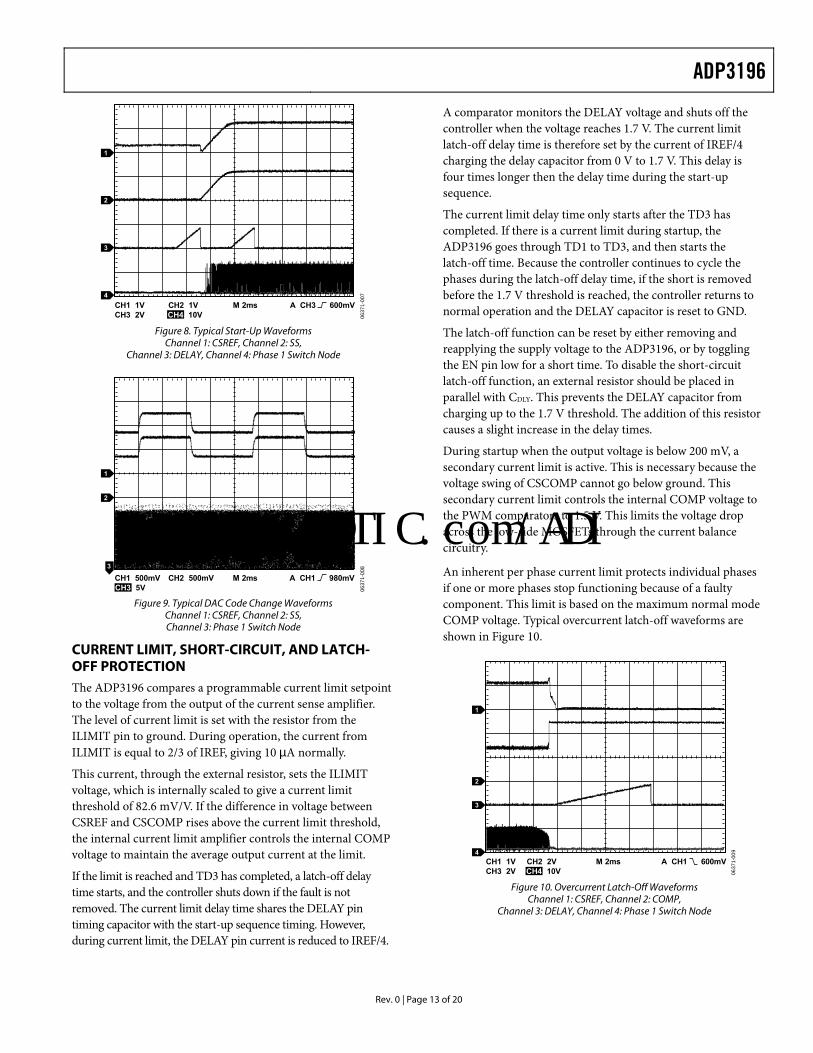
CURRENT LIMIT, SHORT-CIRCUIT, AND LATCH-OFF PROTECTION The ADP3196 compares a programmable current limit setpoint to the voltage from the output of the current sense amplifier. The level of current limit is set with the resistor from the ILIMIT pin to ground. During operation, the current from ILIMIT is equal to 2/3 of IREF, giving 10 µA normally.
This current, through the external resistor, sets the ILIMIT voltage, which is internally scaled to give a current limit threshold of 82.6 mV/V. If the difference in voltage between CSREF and CSCOMP rises above the current limit threshold, the internal current limit amplifier controls the internal COMP voltage to maintain the average output current at the limit.
If the limit is reached and TD3 has completed, a latch-off delay time starts, and the controller shuts down if the fault is not removed. The current limit delay time shares the DELAY pin timing capacitor with the start-up sequence timing. However, during current limit, the DELAY pin current is reduced to IREF/4.
A comparator monitors the DELAY voltage and shuts off the controller when the voltage reaches 1.7 V. The current limit latch-off delay time is therefore set by the current of IREF/4 charging the delay capacitor from 0 V to 1.7 V. This delay is four times longer then the delay time during the start-up sequence.
The current limit delay time only starts after the TD3 has completed. If there is a current limit during startup, the ADP3196 goes through TD1 to TD3, and then starts the latch-off time. Because the controller continues to cycle the phases during the latch-off delay time, if the short is removed before the 1.7 V threshold is reached, the controller returns to normal operation and the DELAY capacitor is reset to GND.
The latch-off function can be reset by either removing and reapplying the supply voltage to the ADP3196, or by toggling the EN pin low for a short time. To disable the short-circuit latch-off function, an external resistor should be placed in parallel with CDLY. This prevents the DELAY capacitor from charging up to the 1.7 V threshold. The addition of this resistor causes a slight increase in the delay times.
During startup when the output voltage is below 200 mV, a secondary current limit is active. This is necessary because the voltage swing of CSCOMP cannot go below ground. This secondary current limit controls the internal COMP voltage to the PWM comparators to 1.5 V. This limits the voltage drop across the low-side MOSFETs through the current balance circuitry.
An inherent per phase current limit protects individual phases if one or more phases stop functioning because of a faulty component. This limit is based on the maximum normal mode COMP voltage. Typical overcurrent latch-off waveforms are shown in Figure 10.
0637
1-00
9
CH4 10VCH2 2VCH1 1V
CH3 2VM 2ms A CH1 600mV
1
2
3
4
Figure 10. Overcurrent Latch-Off Waveforms
Channel 1: CSREF, Channel 2: COMP, Channel 3: DELAY, Channel 4: Phase 1 Switch Node
www.BDTIC.com/ADI
ADP3196
Rev. 0 | Page 14 of 20
DYNAMIC VID The ADP3196 has the ability to respond to dynamically changing VID inputs while the controller is running. This allows the output voltage to change while the supply is running and supplying current to the load. This is commonly referred to as VID on-the-fly (OTF). A VID OTF can occur under either light or heavy load conditions. The processor signals the controller by changing the VID inputs in multiple steps from the start code to the finish code. This change can be positive or negative.
When a VID input changes state, the ADP3196 detects the change and ignores the DAC inputs for a minimum of 400 ns. This time prevents a false code due to logic skew while the six VID inputs are changing. Additionally, the first VID change initiates the PWRGD and CROWBAR blanking functions for a minimum of 100 μs to prevent a false PWRGD or CROWBAR event. Each VID change resets the internal timer.
POWER-GOOD MONITORING The power-good comparator monitors the output voltage via the CSREF pin. The PWRGD pin is an open-drain output whose high level, when connected to a pull-up resistor, indicates that the output voltage is within the nominal limits specified based on the VID voltage setting. PWRGD goes low if the output voltage is outside of this specified range, if the VID DAC inputs are in no CPU mode, or if the EN pin is pulled low. PWRGD is blanked during a VID OTF event for a period of 200 μs to prevent false signals during the time the output is changing.
The PWRGD circuitry also incorporates an initial turn-on delay time (TD3) based on the DELAY timer. Prior to the SS voltage reaching the programmed VID DAC voltage and the PWRGD masking time finishing, the PWRGD pin is held low. Once the SS pin is within 50 mV of the programmed DAC voltage, the capacitor on the DELAY pin begins to charge. A comparator monitors the DELAY voltage and enables PWRGD when the voltage reaches 1.7 V. The PWRGD delay time is set, therefore, by a current of IREF charging a capacitor from 0 V to 1.7 V.
OUTPUT CROWBAR To protect the load and output components of the supply, the PWM outputs are driven low which turns on the low-side MOSFETs when the output voltage exceeds the upper crowbar threshold.
Turning on the low-side MOSFETs pulls down the output as the reverse current builds up in the inductors. If the output overvoltage is due to a short in the high-side MOSFET, this action current limits the input supply or blows its fuse, protecting the microprocessor from being destroyed.
OUTPUT ENABLE AND UVLO For the ADP3196 to begin switching, the input supply (VCC) to the controller must be higher than the UVLO threshold, the EN pin must be higher than its 0.8 V threshold, and the DAC code must be valid. This initiates a system start-up sequence. If either UVLO or EN is less than their respective thresholds, the ADP3196 is disabled. This holds the PWM outputs at ground, shorts the DELAY capacitor to ground, and forces PWRGD, and OD signals low.
In the application circuit, the OD pin should be connected to the OD inputs of the ADP3120A drivers. Grounding OD disables the drivers such that both DRVH and DRVL are grounded. This feature is important in preventing the discharge of the output capacitors when the controller is shut off. If the driver outputs are not disabled, a negative voltage can be generated during output due to the high current discharge of the output capacitors through the inductors.
THERMAL MONITORING The ADP3196 includes a thermal monitoring circuit to detect when a point on the VR has exceeded two different user-defined temperatures. The thermal monitoring circuit requires an NTC thermistor to be placed between TTSENSE and GND. A fixed current of 8 × IREF (normally giving 123 μA) is sourced out of the TTSENSE pin and into the thermistor. The current source is internally limited to 5 V. An internal circuit compares the TTSENSE voltage to a 1.105 V and a 0.81 V threshold and outputs an open-drain signal at the VRM_OFF and VRMHOT outputs, respectively.
The VRM_HOT open-drain output goes high once the voltage on the TTSENSE pin goes below the VRM_HOT thresholds and signals the system that an overtemperature event has occurred. The VRM_OFF output asserts when the voltage on the TTSENSE pin exceeds the VRM_OFF threshold. Because the TTSENSE voltage changes slowly with respect to time, 50 mV of hysteresis is built into these comparators. The thermal monitoring circuitry does not depend on EN and is active when UVLO is above its threshold. When UVLO is below its threshold, VRFAN and VRHOT are forced low.
www.BDTIC.com/ADI

ADP3196
Rev. 0 | Page 15 of 20
Table 4. VID Codes OUTPUT VID5 VID4 VID3 VID2 VID1 VID01.550 0 0 0 0 0 01.525 0 0 0 0 0 11.500 0 0 0 0 1 01.475 0 0 0 0 1 11.450 0 0 0 1 0 01.425 0 0 0 1 0 11.400 0 0 0 1 1 01.375 0 0 0 1 1 11.350 0 0 1 0 0 01.325 0 0 1 0 0 11.300 0 0 1 0 1 01.275 0 0 1 0 1 11.250 0 0 1 1 0 01.225 0 0 1 1 0 11.200 0 0 1 1 1 01.175 0 0 1 1 1 11.150 0 1 0 0 0 01.125 0 1 0 0 0 11.100 0 1 0 0 1 01.075 0 1 0 0 1 11.050 0 1 0 1 0 01.025 0 1 0 1 0 11.000 0 1 0 1 1 00.975 0 1 0 1 1 10.950 0 1 1 0 0 00.925 0 1 1 0 0 10.900 0 1 1 0 1 00.875 0 1 1 0 1 10.850 0 1 1 1 0 00.825 0 1 1 1 0 10.800 0 1 1 1 1 00.775 0 1 1 1 1 1
OUTPUT VID5 VID4 VID3 VID2 VID1 VID00.7625 1 0 0 0 0 00.7500 1 0 0 0 0 10.7375 1 0 0 0 1 00.7250 1 0 0 0 1 10.7125 1 0 0 1 0 00.7000 1 0 0 1 0 10.6875 1 0 0 1 1 00.6750 1 0 0 1 1 10.6625 1 0 1 0 0 00.6500 1 0 1 0 0 10.6375 1 0 1 0 1 00.6250 1 0 1 0 1 10.6125 1 0 1 1 0 00.6000 1 0 1 1 0 10.5875 1 0 1 1 1 00.5750 1 0 1 1 1 10.5625 1 1 0 0 0 00.5500 1 1 0 0 0 10.5375 1 1 0 0 1 00.5250 1 1 0 0 1 10.5125 1 1 0 1 0 00.5000 1 1 0 1 0 10.4875 1 1 0 1 1 00.4750 1 1 0 1 1 10.4625 1 1 1 0 0 00.4500 1 1 1 0 0 10.4375 1 1 1 0 1 00.4250 1 1 1 0 1 10.4125 1 1 1 1 0 00.4000 1 1 1 1 0 10.3875 1 1 1 1 1 00.3750 1 1 1 1 1 1
www.BDTIC.com/ADI
ADP3196
Rev. 0 | Page 16 of 20
1 FOR
A D
ESC
RIP
TIO
N O
F O
PTIO
NA
L R
SW R
ESIS
TOR
S, S
EE T
HE
THEO
RY
OF
OPE
RA
TIO
N S
ECTI
ON
.2 C
ON
NE
CT
NE
AR
EA
CH
IND
UC
TOR
.
1 2 3
8 7 6
45
BST
IN VCC
DR
VH SW
PGN
D
DR
VL
U1
AD
P319
6
1 2 3
8 7 6
45
BST
IN VCC
DR
VH SW
PGN
D
DR
VL
U5
AD
P312
0A
U4
AD
P312
0A
U3
AD
P312
0A
1 2 3
8 7 6
45
BST
IN VCC
DR
VH SW
PGN
D
DR
VL
PWM
1PW
M2
PWM
3PW
M4
NC
SW1
SW2
SW3
SW4
IMO
N
VID0VID1VID2VID3VID4VID5
NCNC
VCC
ILIMITRTRAMPADJLLSETCSREFCSSUMCSCOMPGNDODIREF
EN PWR
GD
FBR
TNFB C
OM
PSS D
ELA
YVR
M_O
FFVR
MH
OT
TTSE
NSE
1
40
R3
1ΩC
81n
FCB
630p
F
RB
2kΩ
RTH
110
0kΩ
, 5%
NTC
RLI
M16
0kΩ 1%
RIR
EF10
0kΩ
RC
S288
.7kΩ
RC
S135
.7kΩ
RPH
314
0kΩ 1%
RPH
414
0kΩ
1%
RPH
214
0kΩ 1%
RPH
114
0kΩ 1%
RSW
41
RSW
31
RSW
21
RSW
11
RT
130kΩ 1%
RA
18.7
kΩ
CFB
16pF
CD
LY18
nF
CSS
10nF
C3
100µ
F(C
3 O
PTIO
NA
L)
+C
41µ
F
680Ω
12V
680Ω
1kΩ
V IN
12V
V IN
RTN
C1
C2
C6
0.1µ
F
C7
1nF
CC
S11n
F5%
NPO
CC
S21n
F5%
NPO
C22
4.7µ
FC18
4.7µ
F
C5
1nF
CA
630p
F
POW
ER G
OO
D
VTT
I/O
VRM
_OFF
VRM
HO
T
1µF
R2
169kΩ 1%
R7
2.2Ω
L137
0nH
18A
2700
µF/1
6V/3
.3A
×2SA
NYO
MV-
WX
SER
IES
++
C14
4.7µ
F
D5
1N41
48D4
1N41
48D3
1N41
48
C21
18nF
R6
2.2Ω
C17
18nF
R5
2.2Ω
C13
18nF
Q10
IPD
09N
03L
Q7
IPD
09N
03L
Q8
IPD
09N
03L
Q
9IP
D09
N03
L
Q11
IPD
09N
03L
Q
12IP
D09
N03
L
C23
10nF
C24
4.7µ
F
C19
10nFC15
10nF
C20
4.7µ
F
L528
0nH
/1.4
mΩ
L428
0nH
/1.4
mΩ
Q4
IPD
09N
03L
Q5
IPD
09N
03L
Q
6IP
D09
N03
L
C16
4.7µ
F
L328
0nH
/1.4
mΩ
1 2 3
8 7 6
45
BST
IN OD
VCC
DR
VH SW
PGN
D
DR
VL
U2
AD
P312
0A
C10
4.7µ
F
D2
1N41
48
R4
2.2Ω
C9
18nF
C25
C32
C11
10nF
Q1
IPD
09N
03L
Q2
IPD
09N
03L
Q
3IP
D09
N03
L
560µ
F/4V
× 7
SAN
YO S
EPC
SER
IES
5mΩ
EA
CH
C12
4.7µ
F
L228
0nH
/1.4
mΩ
RTH
210
0kΩ
, 5%
NTC10
Ω2
10Ω
2
10Ω
2
10Ω
2+
+
V CC
(CO
RE)
0.37
5VTO
1.5
5V10
0A T
DC
V CC
(SEN
SE)
V SS(
SEN
SE)
V CC
(CO
RE)
RTN
10µF
× 8
MLC
C
06371-010
OD
OD
OD
FRO
M C
PU
NC
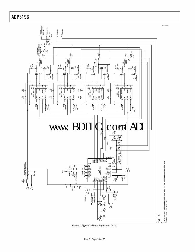
Figure 11.Typical 4-Phase Application Circuit
www.BDTIC.com/ADI

ADP3196
Rev. 0 | Page 17 of 20
LAYOUT AND COMPONENT PLACEMENT The following guidelines are recommended for optimal performance of a switching regulator in a PC system.
General Recommendations
For good results, a PCB with at least four layers is recommended. This provides the needed versatility for control circuitry interconnections with optimal placement, power planes for ground, input and output power, and wide interconnection traces in the remainder of the power delivery current paths. Keep in mind that each square unit of 1-ounce copper trace has a resistance of ~0.53 mΩ at room temperature.
Whenever high currents must be routed between PCB layers, use vias liberally to create several parallel current paths, so the resistance and inductance introduced by these current paths is minimized and the via current rating is not exceeded.
If critical signal lines (including the output voltage sense lines of the ADP3196) must cross through power circuitry, it is best to interpose a signal ground plane between those signal lines and the traces of the power circuitry. This serves as a shield to minimize noise injection into the signals at the expense of making signal ground a bit noisier.
An analog ground plane should be used around and under the ADP3196 as a reference for the components associated with the controller. This plane should be tied to the nearest output decoupling capacitor ground and should not be tied to any other power circuitry to prevent power currents from flowing into it.
The components around the ADP3196 should be located close to the controller with short traces. The most important traces to keep short and away from other traces are the FB pin and CSSUM pin. The output capacitors should be connected as close as possible to the load (or connector), for example, a microproc-essor core, that receives the power. If the load is distributed, the capacitors should also be distributed and generally be in proportion to where the load tends to be more dynamic.
Avoid crossing any signal lines over the switching power path loop (described in the Power Circuitry Recommendations section).
Power Circuitry Recommendations
The switching power path should be routed on the PCB to encompass the shortest possible length to minimize radiated
switching noise energy (EMI) and conduction losses in the board. Failure to take proper precautions often results in EMI problems for the entire PC system and noise-related operational problems in the power converter control circuitry. The switching power path is the loop formed by the current path through the input capacitors and the power MOSFETs, including all interconnecting PCB traces and planes. Using short and wide interconnection traces is especially critical in this path for two reasons: it minimizes the inductance in the switching loop, which can cause high energy ringing; and it accommodates the high current demand with minimal voltage loss.
When a power dissipating component, for example, a power MOSFET, is soldered to a PCB, it is recommended to liberally use the vias, both directly on the mounting pad and immediately surrounding it. Two important reasons for this are improved current rating through the vias and improved thermal perform-ance from vias extended to the opposite side of the PCB, where a plane can more readily transfer the heat to the air. Make a mirror image of any pad being used to heat sink the MOSFETs on the opposite side of the PCB to achieve the best thermal dissipation in the air around the board. To further improve thermal performance, use the largest possible pad area.
The output power path should also be routed to encompass a short distance. The output power path is formed by the current path through the inductor, the output capacitors, and the load.
For best EMI containment, a solid power ground plane should be used as one of the inner layers extending fully under all the power components.
Signal Circuitry Recommendations
The output voltage is sensed and regulated between the FB pin and the FBRTN pin, which connect to the signal ground at the load. To avoid differential mode noise pickup in the sensed signal, the loop area should be small. Thus, the FB trace and FBRTN trace should be routed adjacent to each other on top of the power ground plane back to the controller.
The feedback traces from the switch nodes should be connected as close as possible to the inductor. The CSREF signal should be connected to the output voltage at the nearest inductor to the controller.
www.BDTIC.com/ADI
ADP3196
Rev. 0 | Page 18 of 20
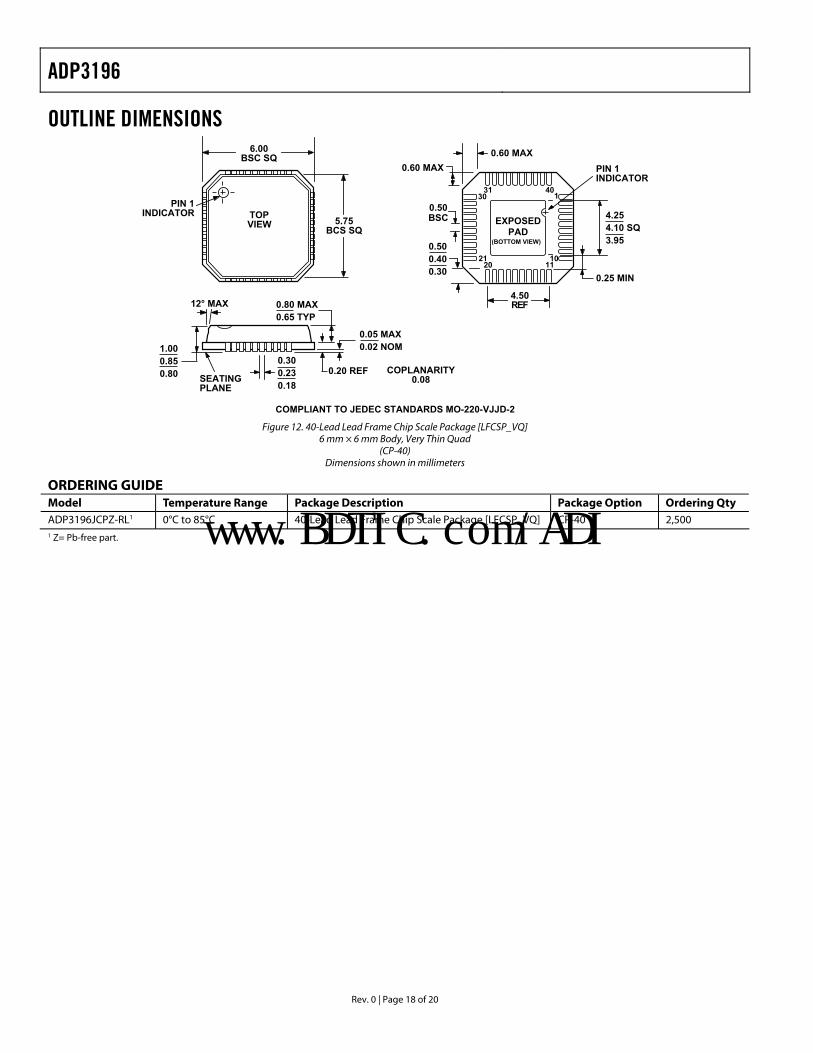
OUTLINE DIMENSIONS
140
1011
3130
2120
4.254.10 SQ3.95
TOPVIEW
6.00BSC SQ
PIN 1INDICATOR
5.75BCS SQ
12° MAX
0.300.230.18
0.20 REFSEATINGPLANE
1.000.850.80
0.05 MAX0.02 NOM
COPLANARITY0.08
0.80 MAX0.65 TYP
4.50REF
0.500.400.30
0.50BSC
PIN 1INDICATOR
0.60 MAX0.60 MAX
0.25 MIN
EXPOSEDPAD
(BOTTOM VIEW)
COMPLIANT TO JEDEC STANDARDS MO-220-VJJD-2 Figure 12. 40-Lead Lead Frame Chip Scale Package [LFCSP_VQ]
6 mm × 6 mm Body, Very Thin Quad (CP-40)
Dimensions shown in millimeters
ORDERING GUIDE Model Temperature Range Package Description Package Option Ordering Qty ADP3196JCPZ-RL1 0°C to 85°C 40-Lead Lead Frame Chip Scale Package [LFCSP_VQ] CP-40 2,500 1 Z= Pb-free part.
www.BDTIC.com/ADI

ADP3196
Rev. 0 | Page 19 of 20
NOTES
www.BDTIC.com/ADI

ADP3196
Rev. 0 | Page 20 of 20
NOTES
©2006 Analog Devices, Inc. All rights reserved. Trademarks and registered trademarks are the property of their respective owners. D06371-0-10/06(0)
www.BDTIC.com/ADI