adn2841 (rev. c) - analog · pdf filedual-loop, 50 mbps to 2.7 gbps laser diode driver data...
TRANSCRIPT
Dual-Loop, 50 Mbps to 2.7 Gbps Laser Diode Driver
Data Sheet ADN2841
Rev. C Document Feedback Information furnished by Analog Devices is believed to be accurate and reliable. However, no responsibility is assumed by Analog Devices for its use, nor for any infringements of patents or other rights of third parties that may result from its use. Specifications subject to change without notice. No license is granted by implication or otherwise under any patent or patent rights of Analog Devices. Trademarks and registered trademarks are the property of their respective owners.
One Technology Way, P.O. Box 9106, Norwood, MA 02062-9106, U.S.A. Tel: 781.329.4700 ©2001–2017 Analog Devices, Inc. All rights reserved. Technical Support www.analog.com
FEATURES 50 Mbps to 2.7 Gbps operation Typical rise/fall time: 80 ps Bias current range: 2 mA to 100 mA Modulation current range: 5 mA to 80 mA Monitor photodiode current: 50 µA to 1200 µA Closed-loop control of power and extinction ratio Laser fail and laser degrade alarms Automatic laser shutdown (ALS) Dual MPD functionality for DWDM Optional clocked data Full current parameter monitoring 5 V operation 48-lead LFCSP 32-lead LFCSP (reduced functionality)
APPLICATIONS DWDM dual MPD wavelength fixing SONET OC-1/3/12/48 SDH STM-1/4/16 Fibre Channel Gigabit Ethernet
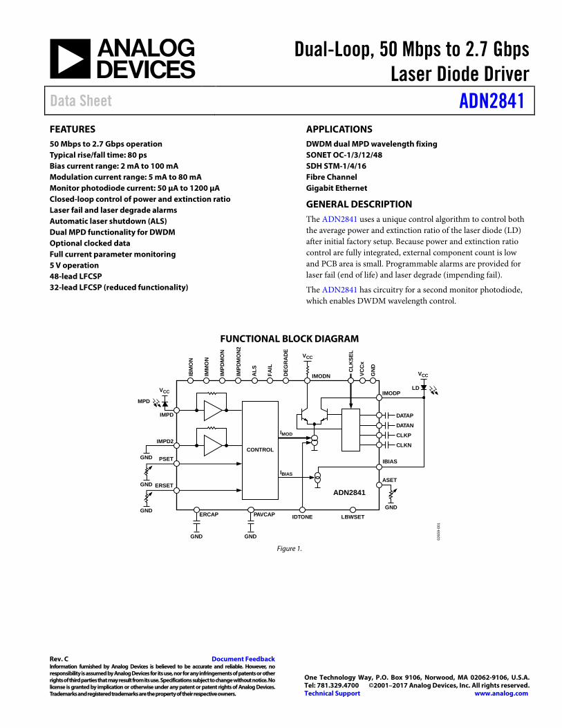
GENERAL DESCRIPTION The ADN2841 uses a unique control algorithm to control both the average power and extinction ratio of the laser diode (LD) after initial factory setup. Because power and extinction ratio control are fully integrated, external component count is low and PCB area is small. Programmable alarms are provided for laser fail (end of life) and laser degrade (impending fail).
The ADN2841 has circuitry for a second monitor photodiode, which enables DWDM wavelength control.
FUNCTIONAL BLOCK DIAGRAM
CONTROL
DATAP
DATAN
CLKP
CLKN
IMODPLD
VCC
GND
ASET
IMOD
IBIAS
GNDGND
GND
GND
GND
LBWSETIDTONEPAVCAPERCAP
ERSET
PSET
IMPD2
IMPD
VCC
MPD
IBM
ON
IMM
ON
IMPD
MO
N
IMPD
MO
N2
ALS
FAIL
DEG
RA
DE
CLK
SEL
VCC
x
GN
D
VCC
ADN2841
IMODN
IBIAS
0265
9-00
1
Figure 1.
ADN2841 Data Sheet
Rev. C | Page 2 of 16
TABLE OF CONTENTS Features .............................................................................................. 1 Applications ....................................................................................... 1 General Description ......................................................................... 1 Functional Block Diagram .............................................................. 1 Revision History ............................................................................... 2 Specifications ..................................................................................... 3 Absolute Maximum Ratings ............................................................ 5
Thermal Resistance ...................................................................... 5 ESD Caution .................................................................................. 5
Pin Configurations and Function Descriptions ........................... 6 Typical Performance Characteristics ............................................. 8 Theory of Operation ........................................................................ 9
Control ........................................................................................... 9 Loop Bandwidth Selection .......................................................... 9
Alarms .............................................................................................9 Monitor Currents ....................................................................... 10 Dual MPD DWDM Function (48-Lead LFCSP Only) ......... 10 IDTONE (48-Lead LFCSP Only) ............................................. 10 Data and Clock Inputs ............................................................... 11 CCBIAS ........................................................................................ 11 Automatic Laser Shutdown ....................................................... 11 Alarm Interfaces ......................................................................... 11 Power Consumption .................................................................. 11
Application Circuits ....................................................................... 12 Outline Dimensions ....................................................................... 15
Ordering Guide .......................................................................... 16
REVISION HISTORY2/2017—Rev. B to Rev. C Changed CP-48-1 to CP-48-4 ...................................... Throughout Changes to Figure 3 and Figure 4 ................................................... 6 Changes to Figure 11 ...................................................................... 12 Changes to Figure 12 ...................................................................... 13 Changes to Figure 13 ...................................................................... 14 Updated Outline Dimensions ....................................................... 15 Changes to Ordering Guide .......................................................... 16 9/2013—Rev. A to Rev. B Updated Format .................................................................. Universal Changes to Table 2 ............................................................................ 5 Added Thermal Resistance Section and Table 3 .......................... 5
Changes to Figure 3, Figure 4, and Table 4 .................................... 6 Added Typical Performance Characteristics Section; moved Figure 5 and Figure 6 ........................................................... 8 Updated Outline Dimensions ....................................................... 15 Changes to Ordering Guide .......................................................... 16 8/2002—Rev. 0 to Rev. A Replaced Figure 8 ........................................................................... 10 Updated Outline Dimensions ....................................................... 11 10/2001—Revision 0: Initial Version

Data Sheet ADN2841
Rev. C | Page 3 of 16
SPECIFICATIONS VCC = 5 V ± 10%. All specifications TMIN to TMAX, unless otherwise noted. Typical values are specified at 25°C.
Table 1. Parameter1 Min Typ Max Unit Test Conditions/Comments LASER BIAS (BIAS)
Current, IBIAS 2 100 mA Compliance Voltage 1.2 VCC V IBIAS During ALS 0.1 mA ALS Response Time 10 μs CCBIAS Compliance Voltage 1.2 V
MODULATION CURRENT (IMODP, IMODN) Output Current, IMOD 5 80 mA Compliance Voltage 1.8 VCC V IMOD During ALS 0.1 mA Rise Time 80 120 ps Fall Time 80 120 ps Jitter 20 ps p-p Pulse Width Distortion 18 ps
MONITOR PD (MPD, MPD2) Input Current 50 1200 μA Average current Voltage 1.6 V
POWER SET INPUT (PSET PIN) Capacitance 80 pF Input Current 50 1200 μA Average current Voltage 1.15 1.23 1.35 V
EXTINCTION RATIO SET INPUT (ERSET PIN) Allowable Resistance Range 1.2 25 kΩ Voltage 1.15 1.23 1.35 V
ALARM SET (ASET PIN) Allowable Resistance Range 1.2 25 kΩ Voltage 1.15 1.23 1.35 V Hysteresis 5 %
CONTROL LOOP Time Constant 0.22 sec LBWSET = GND
2.25 sec LBWSET = VCC DATA INPUTS (DATAP, DATAN, CLKP, CLKN PINS)
AC-Coupled2 V p-p (Single-Ended Peak-to-Peak) 100 500 mV Input Impedance 50 Ω tSETUP
3 150 95 ps tHOLD
3 0 –70 ps LOGIC INPUTS (ALS, LBWSET, CLKSEL PINS)
VIH 2.4 V VIL 0.8 V
ALARM OUTPUTS Internal 30 kΩ pull-up VOH 2.4 V VOL 0.8 V
IDTONE PIN User to supply current sink in the range of 50 μA to 4 mA
Compliance Voltage VCC − 1.5 V IOUT/IIN Ratio 2 fIN
4 0.01 1 MHz
ADN2841 Data Sheet
Rev. C | Page 4 of 16
Parameter1 Min Typ Max Unit Test Conditions/Comments IBMON, IMMON, IMPDMON, IMPDMON2 PINS
IBMON, IMMON Division Ratio 100 A/A IBIAS current/IMOD current IMPDMON, IMPDMON2 Division Ratio 1 A/A IMPD current/IMPD2 current IMPDMON to IMPDMON2 Matching 1 % IMPD = 1200 μA Compliance Voltage 0 VCC − 1.2 V
SUPPLY ICC
5 0.05 A IBIAS = IMOD = 0 A VCC
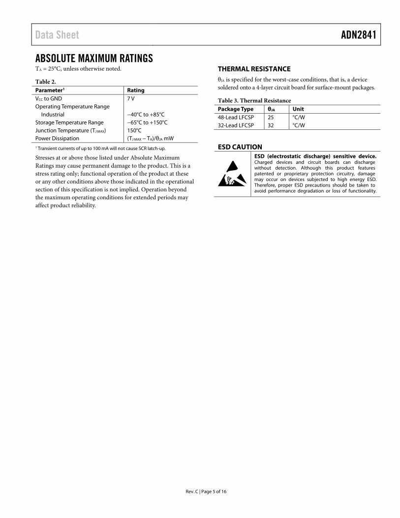
6 4.5 5.0 5.5 V 1 Temperature range: −40°C to +85°C. 2 When the voltage on DATAP is greater than the voltage on DATAN, the modulation current flows in the IMODP pin. 3 Guaranteed by design and characterization. Not production tested. 4 IDTONE may cause eye distortion. 5 ICC for power calculation is the typical ICC given. 6 All VCCx pins should be shorted together.
DATAP/DATAN
SETUP HOLDtHtS
CLKP
0265
9-00
2
Figure 2. Setup and Hold Time
Data Sheet ADN2841
Rev. C | Page 5 of 16
ABSOLUTE MAXIMUM RATINGS TA = 25°C, unless otherwise noted.
Table 2. Parameter1 Rating VCC to GND 7 V Operating Temperature Range
Industrial −40°C to +85°C Storage Temperature Range −65°C to +150°C Junction Temperature (TJ MAX) 150°C Power Dissipation (TJ MAX − TA)/θJA mW 1 Transient currents of up to 100 mA will not cause SCR latch-up.
Stresses at or above those listed under Absolute Maximum Ratings may cause permanent damage to the product. This is a stress rating only; functional operation of the product at these or any other conditions above those indicated in the operational section of this specification is not implied. Operation beyond the maximum operating conditions for extended periods may affect product reliability.
THERMAL RESISTANCE θJA is specified for the worst-case conditions, that is, a device soldered onto a 4-layer circuit board for surface-mount packages.
Table 3. Thermal Resistance Package Type θJA Unit 48-Lead LFCSP 25 °C/W 32-Lead LFCSP 32 °C/W
ESD CAUTION

ADN2841 Data Sheet
Rev. C | Page 6 of 16
PIN CONFIGURATIONS AND FUNCTION DESCRIPTIONS
ADN2841TOP VIEW
(Not to Scale)
GND 1LBWSET 2
ASET 3ERSET 4
PSET 5GND 6
IMPD 7IMPDMON 8
IMPDMON2 9IMPD2 10GND4 11VCC4 12
36 GND235 IDTONE34 GND233 IBMON32 IMMON31 GND330 VCC329 ALS28 FAIL27 DEGRADE26 CLKSEL25 GND
48
CC
BIA
S47
IB
IAS
46
IBIA
S45
G
ND
244
G
ND
243
IM
OD
P42
IM
OD
P41
G
ND
240
IM
OD
N39
IM
OD
N38
V
CC
237
G
ND
2
ER
CA
P
13P
AV
CA
P
14G
ND
15
VC
C1
16
GN
D1
17
DA
TA
N
18D
AT
AP
19
GN
D1
20
CL
KP
21
CL
KN
22
GN
D
23G
ND
24
0265
9-00
3
NOTES1. THE EXPOSED PAD ON THE BOTTOM OF THE PACKAGE
MUST BE CONNECTED TO VCC OR THE GND PLANE.
PIN 1INDICATOR
Figure 3. Pin Configuration, 48-Lead LFCSP
PIN 1INDICATOR
LBWSETASET
ERSETPSETIMPD
IMPDMONGND4VCC4
IBMONIMMONGND3VCC3ALSFAILDEGRADECLKSEL
ER
CA
PP
AV
CA
PV
CC
1D
AT
AN
DA
TA
PG
ND
1C
LK
PC
LK
N
CC
BIA
SIB
IAS
GN
D2
GN
D2
IMO
DP
GN
D2
IMO
DN
VC
C2
0265
9-00
4NOTES1. THE EXPOSED PAD ON THE BOTTOM OF THE PACKAGE
MUST BE CONNECTED TO VCC OR THE GND PLANE.
2423222120191817
12345678
9 10 11 12 13 14 15 16
32 31 30 29 28 27 26 25
ADN2841TOP VIEW
(Not to Scale)
Figure 4. Pin Configuration, 32-Lead LFCSP
Table 4. Pin Function Descriptions Pin No.
48-Lead LFCSP
32-Lead LFCSP Mnemonic Description
1 GND Supply Ground. 2 1 LBWSET Select Low Loop Bandwidth (Active = VCC). 3 2 ASET Alarm Current Threshold Set Pin. 4 3 ERSET Extinction Ratio Set Pin. 5 4 PSET Average Optical Power Set Pin. 6 GND Ground. 7 5 IMPD Monitor Photodiode Input. 8 6 IMPDMON Mirrored Current from Monitor Photodiode. 9 IMPDMON2 Mirrored Current from Monitor Photodiode 2. For use with two MPDs. 10 IMPD2 Monitor Photodiode Input 2. For use with two MPDs. 11 7 GND4 Supply Ground. 12 8 VCC4 Supply Voltage. 13 9 ERCAP Extinction Ratio Loop Capacitor. 14 10 PAVCAP Average Power Loop Capacitor. 15 GND Ground. 16 11 VCC1 Supply Voltage. 17 GND1 Supply Ground. 18 12 DATAN Data, Negative Differential Terminal. 19 13 DATAP Data, Positive Differential Terminal. 20 14 GND1 Supply Ground. 21 15 CLKP Data Clock, Positive Differential Terminal. Used if CLKSEL = VCC. 22 16 CLKN Data Clock, Negative Differential Terminal. Used if CLKSEL = VCC. 23 GND Ground. 24 GND Ground. 25 GND Ground. 26 17 CLKSEL Clock Select (Active = VCC). Used if data is clocked into the chip. 27 18 DEGRADE Degrade Alarm Output.
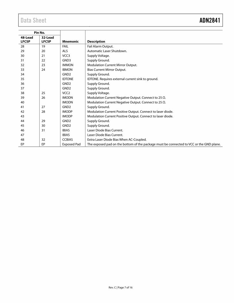
Data Sheet ADN2841
Rev. C | Page 7 of 16
Pin No. 48-Lead LFCSP
32-Lead LFCSP Mnemonic Description
28 19 FAIL Fail Alarm Output. 29 20 ALS Automatic Laser Shutdown. 30 21 VCC3 Supply Voltage. 31 22 GND3 Supply Ground. 32 23 IMMON Modulation Current Mirror Output. 33 24 IBMON Bias Current Mirror Output. 34 GND2 Supply Ground. 35 IDTONE IDTONE. Requires external current sink to ground. 36 GND2 Supply Ground. 37 GND2 Supply Ground. 38 25 VCC2 Supply Voltage. 39 26 IMODN Modulation Current Negative Output. Connect to 25 Ω. 40 IMODN Modulation Current Negative Output. Connect to 25 Ω. 41 27 GND2 Supply Ground. 42 28 IMODP Modulation Current Positive Output. Connect to laser diode. 43 IMODP Modulation Current Positive Output. Connect to laser diode. 44 29 GND2 Supply Ground. 45 30 GND2 Supply Ground. 46 31 IBIAS Laser Diode Bias Current. 47 IBIAS Laser Diode Bias Current. 48 32 CCBIAS Extra Laser Diode Bias When AC-Coupled. EP EP Exposed Pad The exposed pad on the bottom of the package must be connected to VCC or the GND plane.
ADN2841 Data Sheet
Rev. C | Page 8 of 16
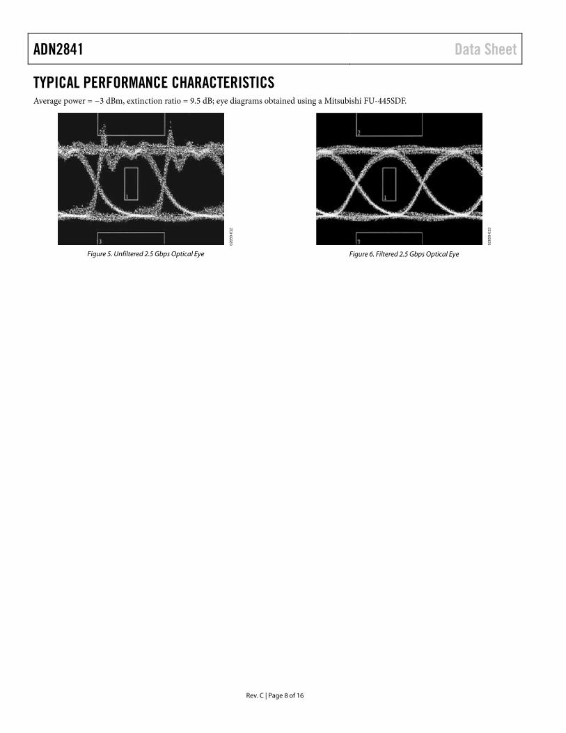
TYPICAL PERFORMANCE CHARACTERISTICS Average power = −3 dBm, extinction ratio = 9.5 dB; eye diagrams obtained using a Mitsubishi FU-445SDF.
0265
9-01
2
Figure 5. Unfiltered 2.5 Gbps Optical Eye
0265
9-01
3
Figure 6. Filtered 2.5 Gbps Optical Eye
Data Sheet ADN2841
Rev. C | Page 9 of 16
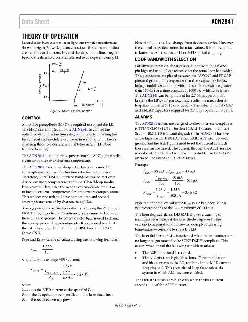
THEORY OF OPERATION Laser diodes have current-in to light-out transfer functions as shown in Figure 7. Two key characteristics of this transfer function are the threshold current, ITH, and the slope in the linear region beyond the threshold current, referred to as slope efficiency, LI.
ER =
PAV =
P1P0
P1 + P02
ΔP
LI =
ITH CURRENT
P1
PAV
P0
OPT
ICA
L PO
WER
ΔPΔIΔI
0265
9-00
5
Figure 7. Laser Transfer Function
CONTROL A monitor photodiode (MPD) is required to control the LD. The MPD current is fed into the ADN2841 to control the optical power and extinction ratio, continuously adjusting the bias current and modulation current in response to the laser’s changing threshold current and light-to-current (LI) slope (slope efficiency).
The ADN2841 uses automatic power control (APC) to maintain a constant power over time and temperature.
The ADN2841 uses closed-loop extinction ratio control to allow optimum setting of extinction ratio for every device. Therefore, SONET/SDH interface standards can be met over device variation, temperature, and time. Closed-loop modu-lation control eliminates the need to overmodulate the LD or to include external components for temperature compensation. This reduces research and development time and second-sourcing issues caused by characterizing LDs.
Average power and extinction ratio are set using the PSET and ERSET pins, respectively. Potentiometers are connected between these pins and ground. The potentiometer RPSET is used to change the average power. The potentiometer RERSET is used to adjust the extinction ratio. Both PSET and ERSET are kept 1.23 V above GND.
RPSET and RERSET can be calculated using the following formulas:
AVPSET I
RV23.1
=
where IAV is the average MPD current.
AVCW
CWMPDERSET
PERER
PIR
××+
−×
=2.0
11
V23.1
_
where IMPD_CW is the MPD current at the specified PCW. PCW is the dc optical power specified on the laser data sheet. PAV is the required average power.
Note that IERSET and IPSET change from device to device. However, the control loops determine the actual values. It is not required to know the exact values for LI or MPD optical coupling.
LOOP BANDWIDTH SELECTION For anyrate operation, the user should hardwire the LBWSET pin high and use 1 μF capacitors to set the actual loop bandwidth. These capacitors are placed between the PAVCAP and ERCAP pins and ground. It is important that these capacitors be low leakage multilayer ceramics with an insulation resistance greater than 100 GΩ or a time constant of 1000 sec, whichever is less. The ADN2841 can be optimized for 2.7 Gbps operation by keeping the LBWSET pin low. This results in a much shorter loop time constant (a 10× reduction). The value of the PAVCAP and ERCAP capacitors required for 2.7 Gbps operation is 22 nF.
ALARMS The ADN2841 alarms are designed to allow interface compliance to ITU-T G.958 (11/94), Section 10.3.1.1.2 (transmit fail) and Section 10.3.1.1.3 (transmit degrade). The ADN2841 has two active high alarms, DEGRADE and FAIL. A resistor between ground and the ASET pin is used to set the current at which these alarms are raised. The current through the ASET resistor is a ratio of 100:1 to the FAIL alarm threshold. The DEGRADE alarm will be raised at 90% of this level.
Example:
μA500100
mA50100
mA45mA50
===
=∴=
BIASTRIPASET
DEGRADEFAIL
II
II
kΩ46.2μA500V23.1V23.1
===ASET
ASET IR
Note that the smallest value for RASET is 1.2 kΩ, because this value corresponds to the IBIAS maximum of 100 mA.
The laser degrade alarm, DEGRADE, gives a warning of imminent laser failure if the laser diode degrades further or if environmental conditions—for example, increasing temperature—continue to stress the LD.
The laser fail alarm, FAIL, is activated when the transmitter can no longer be guaranteed to be SONET/SDH compliant. This occurs when one of the following conditions arises:
• The ASET threshold is reached. • The ALS pin is set high. This shuts off the modulation
and bias currents to the LD, resulting in the MPD current dropping to 0. This gives closed-loop feedback to the system in which ALS has been enabled.
The DEGRADE pin goes high only when the bias current exceeds 90% of the ASET current.
ADN2841 Data Sheet
Rev. C | Page 10 of 16
MONITOR CURRENTS IBMON, IMMON, IMPDMON, and IMPDMON2 are current controlled current sources from VCC. They mirror the bias, modu-lation, and MPD current for increased monitoring functionality. An external resistor to GND gives a voltage proportional to the current monitored.
DUAL MPD DWDM FUNCTION (48-LEAD LFCSP ONLY) The ADN2841 has circuitry for an optional second monitor photodiode, MPD2. The second photodiode current is mirrored to IMPDMON2 for wavelength control purposes and is summed internally for the power control loop. For single MPD circuits, the IMPD2 pin is tied to GND.
The second monitor photodiode enables the system designer to use the two currents to control the wavelength of the laser diode using various optical filtering techniques inside the laser module.
If the monitor current functions IMPDMON and IMPDMON2 are not required, the IMPD and IMPD2 pins can be grounded, and the monitor photodiode output can be connected directly to PSET.
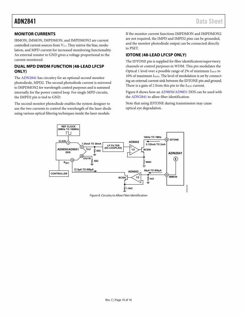
IDTONE (48-LEAD LFCSP ONLY) The IDTONE pin is supplied for fiber identification/supervisory channels or control purposes in WDM. This pin modulates the Optical 1 level over a possible range of 2% of minimum IMOD to 10% of maximum IMOD. The level of modulation is set by connect-ing an external current sink between the IDTONE pin and ground. There is a gain of 2 from this pin to the IMOD current.
Figure 8 shows how an AD9850/AD9851 DDS can be used with the ADN2841 to allow fiber identification.
Note that using IDTONE during transmission may cause optical eye degradation.
AD9850/AD9851DDS
50ΩIOUT
1.25mA TO 20mA
IOUTB50Ω
RSET
CONTROLLER
37.5µA TO 600µA
LP FILTER(DC-COUPLED)
500Ω
BC550
0.125mA TO 2mA
10kHz TO 1MHzIDTONE
ADN2841
35
32IMMON
50µA TO 800µA
1kΩ1/2
AD8602
BC550
1.3kΩ
1/2
AD8602CLKIN
REF CLOCK20MHz TO 180MHz
9
21
20
12
0265
9-00
6
Figure 8. Circuitry to Allow Fiber Identification
Data Sheet ADN2841
Rev. C | Page 11 of 16
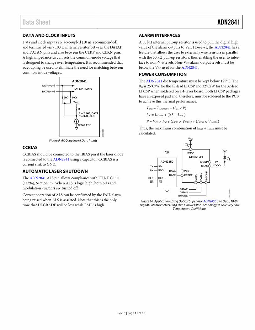
DATA AND CLOCK INPUTS Data and clock inputs are ac-coupled (10 nF recommended) and terminated via a 100 Ω internal resistor between the DATAP and DATAN pins and also between the CLKP and CLKN pins. A high impedance circuit sets the common-mode voltage that is designed to change over temperature. It is recommended that ac coupling be used to eliminate the need for matching between common-mode voltages.
ADN2841
R = 2.5kΩ, DATAR = 3kΩ, CLK
TO FLIP-FLOPS
400µA TYP
DATAP
DATAN
VREG
R
50Ω 50Ω
0265
9-00
7
Figure 9. AC Coupling of Data Inputs
CCBIAS CCBIAS should be connected to the IBIAS pin if the laser diode is connected to the ADN2841 using a capacitor. CCBIAS is a current sink to GND.
AUTOMATIC LASER SHUTDOWN The ADN2841 ALS pin allows compliance with ITU-T G.958 (11/94), Section 9.7. When ALS is logic high, both bias and modulation currents are turned off.
Correct operation of ALS can be confirmed by the FAIL alarm being raised when ALS is asserted. Note that this is the only time that DEGRADE will be low while FAIL is high.
ALARM INTERFACES A 30 kΩ internal pull-up resistor is used to pull the digital high value of the alarm outputs to VCC. However, the ADN2841 has a feature that allows the user to externally wire resistors in parallel with the 30 kΩ pull-up resistors, thus enabling the user to inter-face to non-VCC levels. Non-VCC alarm output levels must be below the VCC used for the ADN2841.
POWER CONSUMPTION The ADN2841 die temperature must be kept below 125°C. The θJA is 25°C/W for the 48-lead LFCSP and 32°C/W for the 32-lead LFCSP when soldered on a 4-layer board. Both LFCSP packages have an exposed pad and, therefore, must be soldered to the PCB to achieve this thermal performance.
TDIE = TAMBIENT + (θJA × P)
ICC = ICCMIN + (0.3 × IMOD)
P = VCC × ICC + (IBIAS × VIBIAS) + (IMOD × VIMODx)
Thus, the maximum combination of IBIAS + IMOD must be calculated.
ADN2841
PSET
ERSET
DATA
P
DATA
N
IDTO
NE
DATAPDATAN
IDTONE
IMODPIBIAS
IMPD
ADN2850
DAC1DAC2
SDISDO
CLK
TxRx
CLKCS
VCC
VCC
VCC
CS
0265
9-00
8
Figure 10. Application Using Optical Supervisor ADN2850 as a Dual, 10-Bit
Digital Potentiometer Using Thin Film Resistor Technology to Give Very Low Temperature Coefficients

ADN2841 Data Sheet
Rev. C | Page 12 of 16
APPLICATION CIRCUITS
GND2 IDT
ON
E
GN
D2
IBM
ON
IMM
ON
GN
D3
VC
C3
AL
S
FA
IL
DE
GR
AD
E
CL
KS
EL
GND
VCC2 GND
IMODN CLKN
IMODN CLKP
GND2 GND1
IMODP DATAP
IMODP DATAN
GND2 GND1
GND2 VCC1
GND
IBIAS
IBIAS
PAVCAP
ERCAPIM
PD
2
IMP
DM
ON
2
IMP
DM
ON
IMP
D
GN
D
PS
ET
ER
SE
T
AS
ET
LB
WS
ET
GN
DG
ND
2
CCBIAS
GN
D
GN
D4
VC
C4
ADN2841
13
24
36 25
FAIL
DEGRADE
DATAP
DATAN
CLKN
CLKP
GND
VCC
100nF 100nF 100nF 100nF 10µF
GND
1 12
1.5kΩ
37
48VCC
VCC
VCC
25Ω
FU-445SDF-WM1
VCC
VCC
VCC
NOTES1. PLACE DECOUPLING CAPACITORS AS CLOSE AS POSSIBLE TO THE
ACTUAL SUPPLY PINS OF THE ADN2841 AND THE LASER DIODE USED. 0265
9-00
9
Figure 11. 2.7 Gbps Test Circuit, DC-Coupled, Data Not Clocked, Fast Loop Time Constant Selected

Data Sheet ADN2841
Rev. C | Page 13 of 16
GND2 IDT
ON
E
GN
D2
IBM
ON
IMM
ON
GN
D3
VC
C3
AL
S
FA
IL
DE
GR
AD
E
CL
KS
EL
GND
VCC2 GND
IMODN CLKN
IMODN CLKP
GND2 GND1
IMODP DATAP
IMODP DATAN
GND2 GND1
GND2 VCC1
GND
IBIAS
IBIAS
PAVCAP
ERCAP
IMP
D2
IMP
DM
ON
2
IMP
DM
ON
IMP
D
GN
D
PS
ET
ER
SE
T
AS
ET
LB
WS
ET
GN
DG
ND
2
CCBIAS
GN
D
GN
D4
VC
C4
ADN2841
13
24
36 25
FAIL
DEGRADE
DATAP
DATAN
CLKN
CLKP
GND
VCC
VCC
100nF 100nF 100nF 100nF 10µF
GND
1 12
1.5kΩ
37
48
VCC
VCC
25Ω
VCC
VCC
VCC
VCC
NOTES1. PLACE DECOUPLING CAPACITORS AS CLOSE AS POSSIBLE TO THE
ACTUAL SUPPLY PINS OF THE ADN2841 AND THE LASER DIODE USED.
VCC
0265
9-01
0
Figure 12. Anyrate Test Circuit, Capacitively Coupled, Data Clocked, Slow Loop Time Constant Selected

ADN2841 Data Sheet
Rev. C | Page 14 of 16
NOTES1. PLACE DECOUPLING CAPACITORS AS CLOSE AS POSSIBLE TO THE ACTUAL
SUPPLY PINS OF THE ADN2841 AND THE LASER DIODE USED.2. THE OP293 HAS BEEN SELECTED BECAUSE OF ITS GAIN BANDWIDTH PRODUCT
AND SHOULD BE USED IN THIS APPLICATION.
GN
D2
IDTONE
GND2
IBMON
IMMON
GND3
VCC3
ALS
FAIL
DEGRADE
CLKSEL
GN
D
VC
C2
GN
D
IMO
DN
CL
KN
IMO
DN
CL
KP
GN
D2
GN
D1
IMO
DP
DA
TA
P
IMO
DP
DA
TA
N
GN
D2
GN
D1
GN
D2
VC
C1
GN
D
IBIA
S
IBIA
S
PA
VC
AP
ER
CA
P
IMPD2
IMPDMON2
IMPDMON
IMPD
GND
PSET
ERSET
ASET
LBWSET
GND GND2CC
BIA
S
GND
GND4
VCC4
ADN2841
13 24
25
36
3748
1
12
VCC
VCC
VCC VCC
–VCC
76
5
1/2OP293
DAC
VCC
128
31/2
OP293DAC
1kΩ
1kΩ
VCC
VCC
VCC
VCC
VCC VCC
VCC
32Ω
VCC
75Ω
100nH 10nF
EA MODULATOR
0265
9-01
1
Figure 13. Applications Circuit
Data Sheet ADN2841
Rev. B | Page 15 of 16
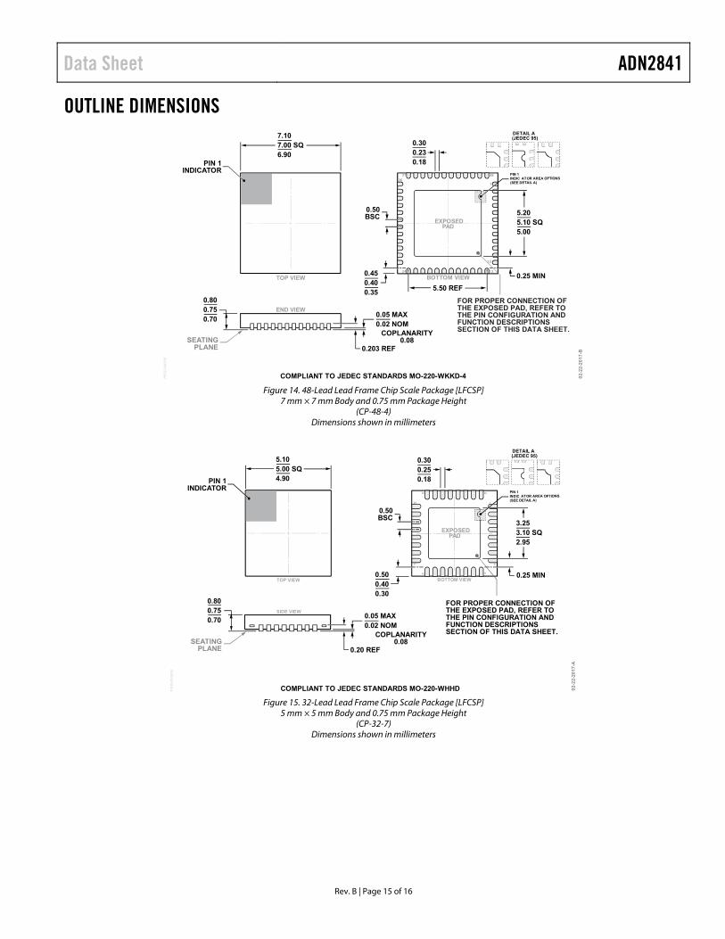
OUTLINE DIMENSIONS
0.450.400.35
0.25 MIN
COMPLIANT TO JEDEC STANDARDS MO-220-WKKD-4
1
12
0.50BSC
BOTTOM VIEWTOP VIEW
PIN 1INDICATOR
48
1324
3637
0.800.750.70
0.05 MAX0.02 NOM
0.203 REF
COPLANARITY0.08
0.300.230.18
02
-22
-201
7-B
7.107.00 SQ6.90
5.50 REF
END VIEW
EXPOSEDPAD
PK
G-0
04
50
9
SEATINGPLANE
5.205.10 SQ5.00
PIN 1INDIC ATOR AREA OPTIONS(SEE DETAIL A)
DETAIL A(JEDEC 95)
FOR PROPER CONNECTION OFTHE EXPOSED PAD, REFER TOTHE PIN CONFIGURATION ANDFUNCTION DESCRIPTIONSSECTION OF THIS DATA SHEET.
Figure 14. 48-Lead Lead Frame Chip Scale Package [LFCSP]
7 mm × 7 mm Body and 0.75 mm Package Height (CP-48-4)
Dimensions shown in millimeters
3.253.10 SQ2.95
0.800.750.70
1
0.50BSC
BOTTOM VIEWTOP VIEW
PIN 1INDICATOR
32
916
17
24
25
8
0.05 MAX0.02 NOM
0.20 REF
COPLANARITY0.08
0.300.250.18
5.105.00 SQ4.90
0.500.400.30
0.25 MIN0
2-2
2-2
01
7-A
COMPLIANT TO JEDEC STANDARDS MO-220-WHHDPK
G-0
03
89
8
SEATINGPLANE
EXPOSEDPAD
SIDE VIEW
PIN 1INDIC ATOR AREA OPTIONS(SEE DETAIL A)
DETAIL A(JEDEC 95)
FOR PROPER CONNECTION OFTHE EXPOSED PAD, REFER TOTHE PIN CONFIGURATION ANDFUNCTION DESCRIPTIONSSECTION OF THIS DATA SHEET.
Figure 15. 32-Lead Lead Frame Chip Scale Package [LFCSP]
5 mm × 5 mm Body and 0.75 mm Package Height (CP-32-7)
Dimensions shown in millimeters
ADN2841 Data Sheet
Rev. C | Page 16 of 16
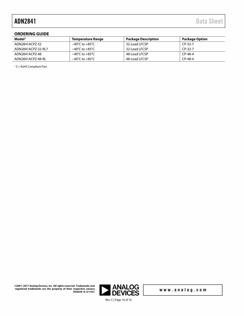
ORDERING GUIDE Model1 Temperature Range Package Description Package Option ADN2841ACPZ-32 −40°C to +85°C 32-Lead LFCSP CP-32-7 ADN2841ACPZ-32-RL7 −40°C to +85°C 32-Lead LFCSP CP-32-7 ADN2841ACPZ-48 −40°C to +85°C 48-Lead LFCSP CP-48-4 ADN2841ACPZ-48-RL −40°C to +85°C 48-Lead LFCSP CP-48-4 1 Z = RoHS Compliant Part.
©2001–2017 Analog Devices, Inc. All rights reserved. Trademarks and registered trademarks are the property of their respective owners. D02659–0–2/17(C)