adf7020-xdbx eval note
DESCRIPTION
ADF7020 Evaluation boardTRANSCRIPT

Tuesday, Oct 16, 2007 4:05 PM
Evaluation Boards for ADF7020& ADF7020-1 ISM Band Transceiver
Preliminary Technical Data EVAL-ADF7020-XDBX
Rev. Pr D Information furnished by Analog Devices is believed to be accurate and reliable. However, no responsibility is assumed by Analog Devices for its use, nor for any infringements of patents or other rights of third parties that may result from its use. Specifications subject to change without notice. No license is granted by implication or otherwise under any patent or patent rights of Analog Devices. Trademarks and registered trademarks are the property of their respective companies.
One Technology Way, P.O. Box 9106, Norwood, MA 02062-9106, U.S.A. Tel: 781.329.4700 www.analog.com Fax: 781.326.8703 © 2007 Analog Devices, Inc. All rights reserved.
FEATURES
ADF7020 & ADF7020-1 ISM Band Transceiver Radio module Can plug into basic mother board (EVAL-ADF70XXMBZ) or development platform with embedded microcontroller (EVAL-ADF70XXMBZ2) RF daughter-card designed on low-cost 2-layer PCB as reference design for cost-sensitive applications Combined output matching circuit (no external antenna switch) optimized at several different frequency ranges Software programmable modulation schemes; GFSK/ FSK/ ASK/OOK/G-ASK PC Software for Register Programming Loop filter setup for operation upto 50kbps. Higher data-rates possible by altering PLL loop filter.
GENERAL DESCRIPTION The ADF7020 and ADF7020-1 are FSK/GFSK/ASK/OOK transceivers which are designed for operation in the licensed and unlicensed VHF/UHF bands from 80MHz to 956MHz. There are different versions of the evaluation daughter board available, each optimized for different frequency bands, see Table 1. The daughter-board contains all the required components for operation of the radio, including loop filter, output matching, antenna and connector to mother board.
To control the ADF7020/ADF7020-1 via the PC you will need the EVAL-ADF70XXMBZ2 mother board. This technical note describes usage with the EVAL-ADF70XXMBZ2 boards (PCB RevD and higher). This is a multi-function board that can be used for:
• detailed evaluation and RF testing of the parts.
• running the ADIismLINK protocol to evaluate the ADF7xxx performance in a networked environment, perform range testing and Packet Error Rate (PER) tests
• run the low-level device drivers, to perform timing critical tests or simply to patch into existing firmware.
Table 1: Ordering Codes
Board Number RF Band Rx Data Rate Tx Data Rate1 Loop Bandwidth2
EVAL-ADF70XXMBZ3 Not for new designs - - - EVAL-ADF70XXMBZ2 Recommended - - - EVAL-ADF7020DBZ1 902 MHz – 928 MHz Up to 200 kbps Up to 50 kbps 50 kHz EVAL-ADF7020DBZ2 862 MHz - 870 MHz Up to 200 kbps Up to 50 kbps 50 kHz EVAL-ADF7020DBZ3 433 MHz - 445 MHz Up to 200 kbps Up to 50 kbps 50 kHz EVAL-ADF7020-1DBZ4 405 MHz - 435 MHz Up to 200 kbps Up to 50 kbps 50 kHz EVAL-ADF7020-1DBZ6 470 MHz - 510 MHz Up to 200 kbps Up to 50 kbps 50 kHz EVAL-ADF7020-1DBZ7 310 MHz – 340 MHz Up to 200 kbps Up to 50 kbps 50 kHz EVAL-ADF7020-1DBZ8 128 MHz – 142 MHz Up to 200 kbps Up to 50 kbps 50 kHz
EVAL-ADF7020-1DBZ5 RF Match/Loop filter not inserted - - -
1. The data rate may be increased by increasing the PLL Loop Bandwidth, see Page10 or use ADI SRD Design Studio. 2. Optimized for FSK. For ASK or OOK typically need to increase the Loop BW to greater than 100kHz to avoid VCO pulling 3. Simple mother board using parallel port interface, not recommended for new designs.

EVAL-ADF7020-XDBX Preliminary Technical Data
Rev. Pr D | Page 2 of 29
Table of contents
Hardware description.........................................................................................................................................................................................................3
ADF7xxx configuration software description ................................................................................................................................................................5
Getting started with the adf7020/-1 .................................................................................................................................................................................6
Setting up an RF Link using ADIismLink.......................................................................................................................................................................8
Bill of Materials................................................................................................................................................................................................................ 10
Installing the USB drivers for the EVAL-ADF70XXMBZ2 board............................................................................................................................ 18
SCHEMATICS ................................................................................................................................................................................................................. 23
Preliminary Technical Data EVAL-ADF7020DBX
Rev. Pr D | Page 3 of 29
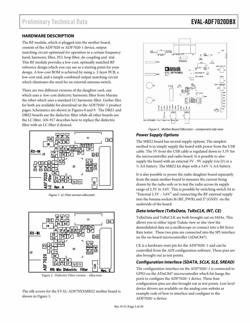
HARDWARE DESCRIPTION The RF module, which is plugged into the mother board, consists of the ADF7020 or ADF7020-1 device, output matching circuit optimized for operation in a certain frequency band, harmonic filter, PLL loop filter, de-coupling and xtal. This RF module provides a low-cost, optimally matched RF reference design which you can use as a starting point for your design. A low-cost BOM is achieved by using a 2-layer PCB, a low-cost xtal, and a simple combined output matching circuit which eliminates the need for an external antenna switch.
There are two different versions of the daughter card, one which uses a low-cost dielectric harmonic filter from Murata the other which uses a standard LC harmonic filter. Gerber files for both are available for download on the ADF7020/-1 product pages. Schematics are shown in Figures 8 and 9. The DBZ1 and DBZ2 boards use the dielectric filter while all other boards use the LC filter. AN-917 describes how to replace the dielectric filter with an LC filter if desired.
Figure 1: .LC Filter version-silkscreen
Figure 2. Dielectric Filter version – silkscreen
The silk screen for the EVAL-ADF70XXMBZ2 mother board is shown in Figure 3.
Figure 3. . Mother Board Silkscreen – component side view
Power Supply Options The MBZ2 board has several supply options. The simplest method is to simply supply the board with power from the USB cable. The 5V from the USB cable is regulated down to 3.3V for the microcontroller and radio board. It is possible to also supply the board with an external 5V - 9V supply (via J3) or a ½ AA battery. The MBZ2 kit ships with a 3.6V ½ AA battery.
It is also possible to power the radio daughter board separately from the main mother board to measure the current being drawn by the radio only or to test the radio across its supply range of 2.3V to 3.6V. This is possible by switching switch S4 to “External 2.3V – 3.6V” and connecting the RF external supply into the banana sockets J6 (RF_PWR) and J7 (GND) on the underside of the board.
Data Interface (TxRxData, TxRxCLK, INT, CE) TxRxData and TxRxCLK are both brought out on SMAs. This allows you to either input Txdata view or else view the demodulated data on a oscilloscope or connect into a Bit Error Rate tester. These two pins are connected into the SPI interface on the on-board microcontroller (ADuC847).
CE is a hardware reset pin for the ADF7020/-1 and can be controlled from the ADI configuration software. These pins are also brought out as test points.
Configuration Interface (SDATA, SCLK, SLE, SREAD) The configuration interface on the ADF7020/-1 is connected to GPIO on the ADuC847 microcontroller which bit-bangs the ports to configure the ADF7020/-1 device. These four configuration pins are also brought out as test points. Low level device drivers are available on the analog.com website as example code of how to interface and configure to the ADF7020/-x device.
EVAL-ADF7020-XDBX Preliminary Technical Data
Rev. Pr D | Page 4 of 29
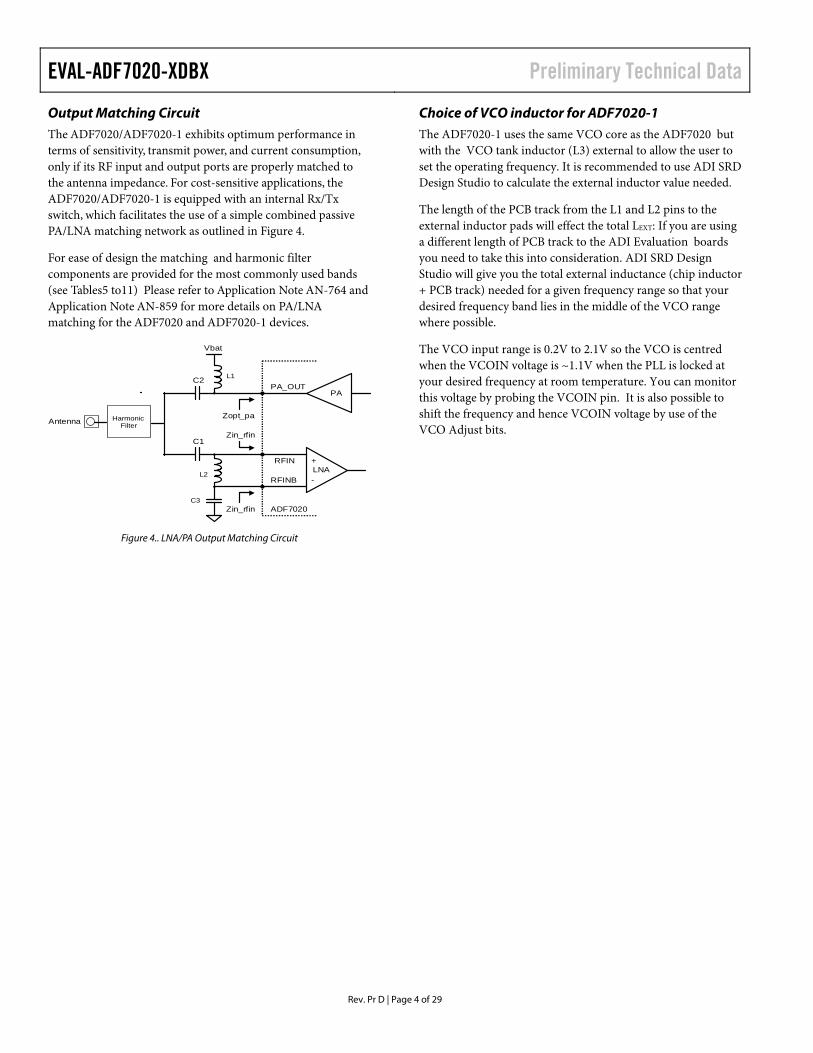
Output Matching Circuit The ADF7020/ADF7020-1 exhibits optimum performance in terms of sensitivity, transmit power, and current consumption, only if its RF input and output ports are properly matched to the antenna impedance. For cost-sensitive applications, the ADF7020/ADF7020-1 is equipped with an internal Rx/Tx switch, which facilitates the use of a simple combined passive PA/LNA matching network as outlined in Figure 4.
For ease of design the matching and harmonic filter components are provided for the most commonly used bands (see Tables5 to11) Please refer to Application Note AN-764 and Application Note AN-859 for more details on PA/LNA matching for the ADF7020 and ADF7020-1 devices.
LNA+
-
PA
ADF7020
PA_OUT
RFIN
RFINB
Vbat
C1
C2
Zopt_pa
Zin_rfin
Zin_rfin
Antenna
L1
L2
C3
HarmonicFilter
Figure 4.. LNA/PA Output Matching Circuit
Choice of VCO inductor for ADF7020-1 The ADF7020-1 uses the same VCO core as the ADF7020 but with the VCO tank inductor (L3) external to allow the user to set the operating frequency. It is recommended to use ADI SRD Design Studio to calculate the external inductor value needed.
The length of the PCB track from the L1 and L2 pins to the external inductor pads will effect the total LEXT: If you are using a different length of PCB track to the ADI Evaluation boards you need to take this into consideration. ADI SRD Design Studio will give you the total external inductance (chip inductor + PCB track) needed for a given frequency range so that your desired frequency band lies in the middle of the VCO range where possible.
The VCO input range is 0.2V to 2.1V so the VCO is centred when the VCOIN voltage is ~1.1V when the PLL is locked at your desired frequency at room temperature. You can monitor this voltage by probing the VCOIN pin. It is also possible to shift the frequency and hence VCOIN voltage by use of the VCO Adjust bits.

Preliminary Technical Data EVAL-ADF7020DBX
Rev. Pr D | Page 5 of 29
ADF7XXX CONFIGURATION SOFTWARE DESCRIPTION Before using the MBZ2 board you should run the “ADF7xxx_ ADIismLINK Install” which contains the relevant USB drivers and setup files for the EVAL-ADF70XXMBZ2. This needs to be done before plugging in the hardware. See Installing USB Drivers section for details.
The ADF7020 /-1 configuration software and the network demo software, ADIismLINK, are also installed as part of the install process. You should check the Analog Devices Website periodically for updates. http://www.analog.com/srd
Once the programs have installed, run ADF7020Rev2_3.exe (or later) from the Analog Devices folder in the Start menu. The window shown below should appear – you will need a screen resolution of 1024 x 768 to use the program.
This is the main window and is divided up into several sections some of which have their own sub-windows which are indicated by a raised button. For example in the PLL Options section, you enter the sub-window by clicking on the “Synth Settings…” button. The green and red toggle buttons turn a feature on or off. You can use the software in stand-alone
mode, that is with the hardware unconnected to calculate register values for example. In this mode the USB button at the bottom of screen should read ‘Connect USB’ and should not be clicked. However in most cases you will want to use the software to control the ADF7020/-1 device. After opening the software, simply click on ‘Connect USB’. Once the software has connected to the target board, the button should change to “Disconnect USB”. The USB comms is now initiated and you should be able to communicate with the device using the software. The software also supports the EVAL-ADF70XXMBZ which uses the parallel port interface.
The software eases the programming challenge by allowing you to input your desired RF frequency, modulation scheme, data-rate etc. and then auto-calculating the ADF7020/-1 register settings based on these inputs. The calculated register settings are displayed in the “Update Registers” panel.
For direct programming of the ADF7020/-1 , click on the “Manual Register Edit” button. This allows you to enter Hex values into individual registers. This is useful for debugging the register settings that you will use in your program code.
Figure 5. Software Front Panel Display
EVAL-ADF7020-XDBX Preliminary Technical Data
Rev. Pr D | Page 6 of 29
GETTING STARTED WITH THE ADF7020/-1 The evaluation performed will be specific to each application, but this section will enable users to familiarise themselves with the features of the ADF7020/ADF7020-1.
Before plugging in the hardware please run “ADF7xxx_ ADIismLINK Install”, which contains the necessary USB drivers and dlls! Note if you have installed ADIismLINK Rev1.0 previously you should also run “purge_ ADIism_ LINK.bat” to remove the old USB setup from the registry.
Initial Hardware Setup As described in the Hardware Description section, the evaluation board is divided into two; an RF module containing the ADF7020/-1 and a mother-board which accepts the RF module and contains the power supply block, analog microcontroller, USB bridge and some I/O pins. You need to mount the RF module onto the mother-board, ensuring correct alignment by having the drill-holes in the module above the supports on the mother board.
There are various power supply options on the board, including the option to power the RF separately to measure RF_IDD and also operate the radio over its full voltage range from 2.3V to 3.6V. The simplest way to power the board is to simply connect the USB cable which provides 5V from the host pc. This 5V is then regulated down to 3.3V for the radio and microcontroller.
Communicating to the Hardware and simple debug To allow register programming of the ADF7020/-1, click on ‘Connect USB’. Once the software has connected to the target hardware, the button should change to “Disconnect USB”.
You will now be able to communicate with the device. To check this you should click on the Readback button and select silicon revision. If you are communicating with the target board and the radio module is plugged in, you should readback a valid code which is then displayed on the top-right of the front panel.
Other useful debug modes to check before proceeding onto the main Tx and Rx evaluation are checking CLKOUT operation on a oscilloscope. By default the CLKOUT frequency should be XTAL/8. You can change this value in the software. Another useful debug point is the voltage on the Regulator pins. This should be approximately 2.2V, when CE is active. You can check this by probing the top of C5 (VREG4 pin) on the RF module.
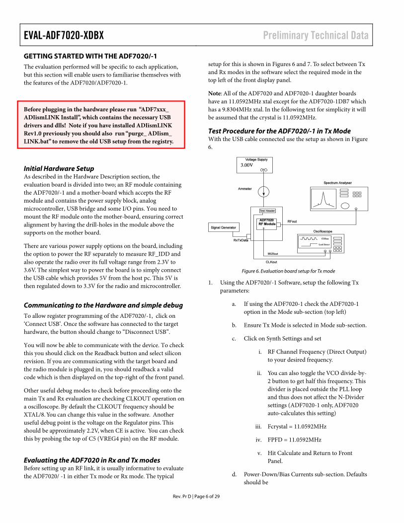
Evaluating the ADF7020 in Rx and Tx modes Before setting up an RF link, it is usually informative to evaluate the ADF7020/ -1 in either Tx mode or Rx mode. The typical
setup for this is shown in Figures 6 and 7. To select between Tx and Rx modes in the software select the required mode in the top left of the front display panel.
Note: All of the ADF7020 and ADF7020-1 daughter boards have an 11.0592MHz xtal except for the ADF7020-1DB7 which has a 9.8304MHz xtal. In the following text for simplicity it will be assumed that the crystal is 11.0592MHz.
Test Procedure for the ADF7020/-1 in Tx Mode With the USB cable connected use the setup as shown in Figure 6.
Figure 6. Evaluation board setup for Tx mode
1. Using the ADF7020/-1 Software, setup the following Tx parameters:
a. If using the ADF7020-1 check the ADF7020-1 option in the Mode sub-section (top left)
b. Ensure Tx Mode is selected in Mode sub-section.
c. Click on Synth Settings and set
i. RF Channel Frequency (Direct Output) to your desired frequency.
ii. You can also toggle the VCO divide-by-2 button to get half this frequency. This divider is placed outside the PLL loop and thus does not affect the N-Divider settings (ADF7020-1 only, ADF7020 auto-calculates this setting)
iii. Fcrystal = 11.0592MHz
iv. FPFD = 11.0592MHz
v. Hit Calculate and Return to Front Panel.
d. Power-Down/Bias Currents sub-section. Defaults should be
Preliminary Technical Data EVAL-ADF7020DBX
Rev. Pr D | Page 7 of 29
rystal oscillator (OSC) ON
e. Mod ns
ar change the power
2. Hit the Program R on on the Software
ely y
4. e Synth Settings sub-window and change the
5. ise is measured by narrowing the span
r
6. n
7. he TxDATA pin and
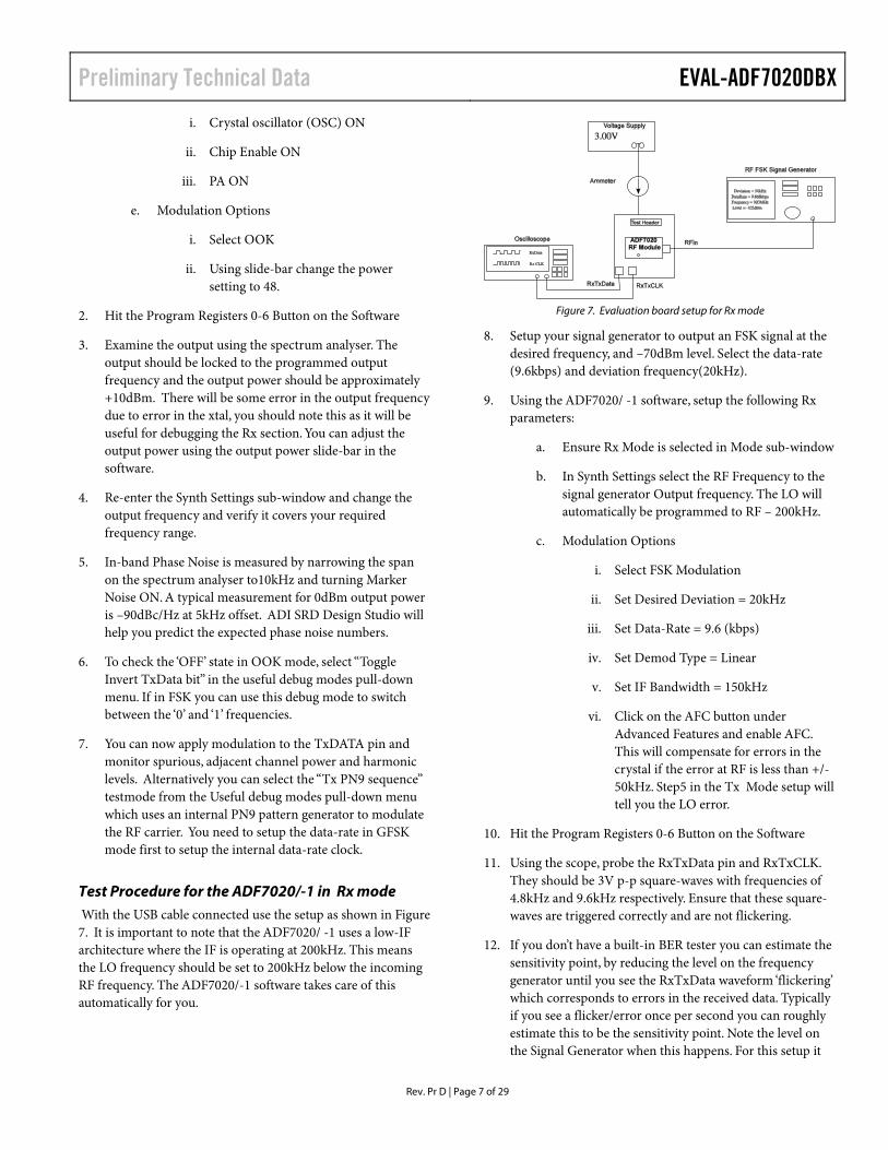
Test Procedure for the ADF7020/-1 in Rx mode igure
g
i. C
ii. Chip Enable ON
iii. PA ON
ulation Optio
i. Select OOK
ii. Using slide-bsetting to 48.
egisters 0-6 Butt
3. Examine the output using the spectrum analyser. The output should be locked to the programmed output frequency and the output power should be approximat+10dBm. There will be some error in the output frequencdue to error in the xtal, you should note this as it will be useful for debugging the Rx section. You can adjust the output power using the output power slide-bar in the software.
Re-enter thoutput frequency and verify it covers your required frequency range.
In-band Phase Noon the spectrum analyser to10kHz and turning Marker Noise ON. A typical measurement for 0dBm output poweis –90dBc/Hz at 5kHz offset. ADI SRD Design Studio will help you predict the expected phase noise numbers.
To check the ‘OFF’ state in OOK mode, select “ToggleInvert TxData bit” in the useful debug modes pull-dowmenu. If in FSK you can use this debug mode to switch between the ‘0’ and ‘1’ frequencies.
You can now apply modulation to tmonitor spurious, adjacent channel power and harmonic levels. Alternatively you can select the “Tx PN9 sequence”testmode from the Useful debug modes pull-down menu which uses an internal PN9 pattern generator to modulate the RF carrier. You need to setup the data-rate in GFSK mode first to setup the internal data-rate clock.
With the USB cable connected use the setup as shown in F7. It is important to note that the ADF7020/ -1 uses a low-IF architecture where the IF is operating at 200kHz. This means the LO frequency should be set to 200kHz below the incominRF frequency. The ADF7020/-1 software takes care of this automatically for you.
Figure 7. Evaluation board setup for Rx mode
8. Setup your signal generator to output an FSK signal at the desired frequency, and –70dBm level. Select the data-rate (9.6kbps) and deviation frequency(20kHz).
9. Using the ADF7020/ -1 software, setup the following Rx parameters:
a. Ensure Rx Mode is selected in Mode sub-window
b. In Synth Settings select the RF Frequency to the signal generator Output frequency. The LO will automatically be programmed to RF – 200kHz.
c. Modulation Options
i. Select FSK Modulation
ii. Set Desired Deviation = 20kHz
iii. Set Data-Rate = 9.6 (kbps)
iv. Set Demod Type = Linear
v. Set IF Bandwidth = 150kHz
vi. Click on the AFC button under Advanced Features and enable AFC. This will compensate for errors in the crystal if the error at RF is less than +/-50kHz. Step5 in the Tx Mode setup will tell you the LO error.
10. Hit the Program Registers 0-6 Button on the Software
11. Using the scope, probe the RxTxData pin and RxTxCLK. They should be 3V p-p square-waves with frequencies of 4.8kHz and 9.6kHz respectively. Ensure that these square-waves are triggered correctly and are not flickering.
12. If you don’t have a built-in BER tester you can estimate the sensitivity point, by reducing the level on the frequency generator until you see the RxTxData waveform ‘flickering’ which corresponds to errors in the received data. Typically if you see a flicker/error once per second you can roughly estimate this to be the sensitivity point. Note the level on the Signal Generator when this happens. For this setup it

EVAL-ADF7020-XDBX Preliminary Technical Data
Rev. Pr D | Page 8 of 29
should be –103dBm +/- 2dBm.
13. Change the demodulator type to correlator in the software and click Update All. Measure the sensitivity again. It should now be better than –108dBm. If using a more accurate Bit Error Rate tester you should measure close to -110.5dBm for a 10E-3 Error rate in correlator mode.
Readback Function It is possible to enable the on-chip ADC on the ADF7020/ -1 and readback a selection of parameters, including battery voltage, temperature(from the on-board temperature sensor), Frequency Error, External voltage and RSSI.
To activate this feature, click on the Readback Toggle button. In the sub-window select the type of readback required. The appropriate value should be displayed on the screen. To check the readback functionality select “Silicon Revision Readback”. Valid codes for the ADF7020 are 0x2007 & 0x2008. Valid readback codes for the ADF7020-1 are 0x2017 & 0x2018.
In Tx mode the ADC is powered-off by default to save power, so in order to readback correctly you need to enable the ADC. This can be done by clicking the status button in the ADC Status section to “ON” before clicking the Readback button. Since the ADC is used in Rx mode for the AGC function, the ADC is powered-on by default in this mode. Thus in Rx mode, valid battery voltage, temperature, frequency error and external voltage readback data can only be retrieved when AGC is disabled. This can be done by manually setting bit 19 (Gain Control) in register 9 (AGC register) low. In practical cases the user would typically do a battery voltage readback in Tx mode or in low-power measure mode. Low-power measure mode is entered by simply bringing CE high, enabling the ADC in Register8, selecting the desired readback value in Register7 and performing the readback
SETTING UP AN RF LINK USING ADIISMLINK
The ADIismLINK software is the simplest way to setup an RF Link. This allows you to perform several functions:
• Setup a wireless star-network and send back sensor data (temperature/accelerometer or user defined) to the basestation to be displayed or logged on the pc.
• transmit simple text messages from Base Station node to remote nodes and vice versa.
• Run a Packet Error Rate (PER) test to test link quality
• Perform range tests without the need for a laptop by powering both boards off a 3.6V battery and displaying the messages on the on-board LEDs.
• Develop user applications on top of the example PHY/MAC layer (Frequency hopping and duty-cycle MAC options)
ADIismLINK can be run on the EVAL-ADF70XXMBZ2 boards and is installed in the Analog Devices folder when you run “ADF7xxx_ADIismLINK Install”.
Preliminary Technical Data EVAL-ADF7020DBX
Rev. Pr D | Page 9 of 29
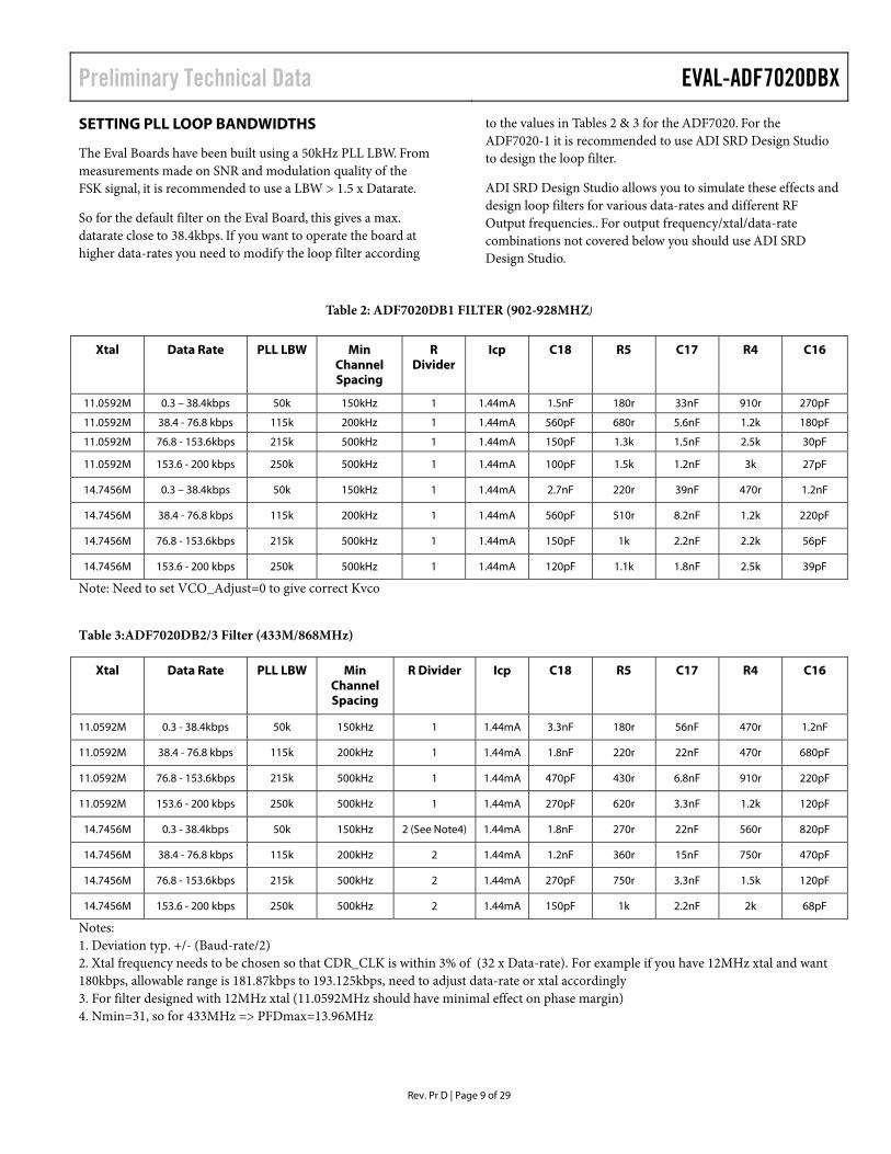
SETTING PLL LOOP BANDWIDTHS
The Eval Boards have been built using a 50kHz PLL LBW. From measurements made on SNR and modulation quality of the FSK signal, it is recommended to use a LBW > 1.5 x Datarate.
So for the default filter on the Eval Board, this gives a max. datarate close to 38.4kbps. If you want to operate the board at higher data-rates you need to modify the loop filter according
to the values in Tables 2 & 3 for the ADF7020. For the ADF7020-1 it is recommended to use ADI SRD Design Studio to design the loop filter.
ADI SRD Design Studio allows you to simulate these effects and design loop filters for various data-rates and different RF Output frequencies.. For output frequency/xtal/data-rate combinations not covered below you should use ADI SRD Design Studio.
Table 2: ADF7020DB1 FILTER (902-928MHZ)
Note: Need to set VCO_Adjust=0 to give correct Kvco
Table 3:ADF7020DB2/3 Filter (433M/868MHz)
Notes: 1. Deviation typ. +/- (Baud-rate/2) 2. Xtal frequency needs to be chosen so that CDR_CLK is within 3% of (32 x Data-rate). For example if you have 12MHz xtal and want 180kbps, allowable range is 181.87kbps to 193.125kbps, need to adjust data-rate or xtal accordingly 3. For filter designed with 12MHz xtal (11.0592MHz should have minimal effect on phase margin) 4. Nmin=31, so for 433MHz => PFDmax=13.96MHz
Xtal Data Rate PLL LBW Min Channel Spacing
R Divider
Icp C18 R5 C17 R4 C16
11.0592M 0.3 – 38.4kbps 50k 150kHz 1 1.44mA 1.5nF 180r 33nF 910r 270pF
11.0592M 38.4 - 76.8 kbps 115k 200kHz 1 1.44mA 560pF 680r 5.6nF 1.2k 180pF
11.0592M 76.8 - 153.6kbps 215k 500kHz 1 1.44mA 150pF 1.3k 1.5nF 2.5k 30pF
11.0592M 153.6 - 200 kbps 250k 500kHz 1 1.44mA 100pF 1.5k 1.2nF 3k 27pF
14.7456M 0.3 – 38.4kbps 50k 150kHz 1 1.44mA 2.7nF 220r 39nF 470r 1.2nF
14.7456M 38.4 - 76.8 kbps 115k 200kHz 1 1.44mA 560pF 510r 8.2nF 1.2k 220pF
14.7456M 76.8 - 153.6kbps 215k 500kHz 1 1.44mA 150pF 1k 2.2nF 2.2k 56pF
14.7456M 153.6 - 200 kbps 250k 500kHz 1 1.44mA 120pF 1.1k 1.8nF 2.5k 39pF
Xtal Data Rate PLL LBW Min Channel Spacing
R Divider Icp C18 R5 C17 R4 C16
11.0592M 0.3 - 38.4kbps 50k 150kHz 1 1.44mA 3.3nF 180r 56nF 470r 1.2nF
11.0592M 38.4 - 76.8 kbps 115k 200kHz 1 1.44mA 1.8nF 220r 22nF 470r 680pF
11.0592M 76.8 - 153.6kbps 215k 500kHz 1 1.44mA 470pF 430r 6.8nF 910r 220pF
11.0592M 153.6 - 200 kbps 250k 500kHz 1 1.44mA 270pF 620r 3.3nF 1.2k 120pF
14.7456M 0.3 - 38.4kbps 50k 150kHz 2 (See Note4) 1.44mA 1.8nF 270r 22nF 560r 820pF
14.7456M 38.4 - 76.8 kbps 115k 200kHz 2 1.44mA 1.2nF 360r 15nF 750r 470pF
14.7456M 76.8 - 153.6kbps 215k 500kHz 2 1.44mA 270pF 750r 3.3nF 1.5k 120pF
14.7456M 153.6 - 200 kbps 250k 500kHz 2 1.44mA 150pF 1k 2.2nF 2k 68pF
EVAL-ADF7020-XDBX Preliminary Technical Data
Rev. Pr D | Page 10 of 29
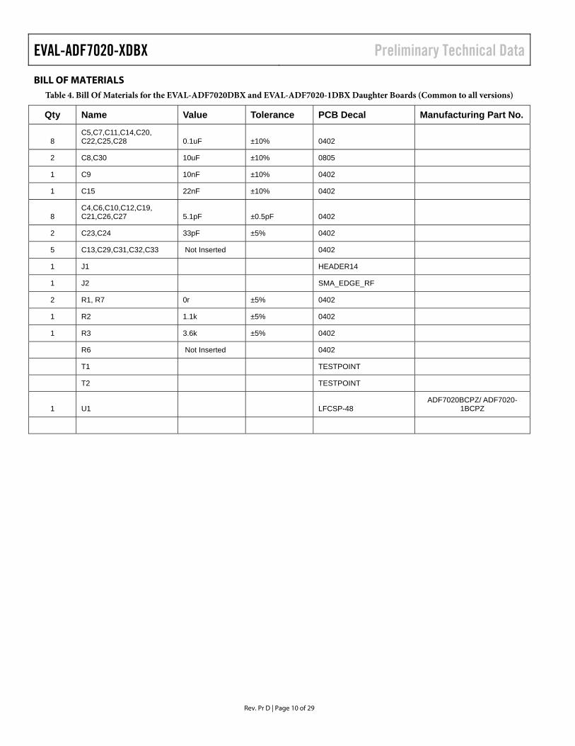
BILL OF MATERIALSTable 4. Bill Of Materials for the EVAL-ADF7020DBX and EVAL-ADF7020-1DBX Daughter Boards (Common to all versions)
Qty Name Value Tolerance PCB Decal Manufacturing Part No.
8 C5,C7,C11,C14,C20, C22,C25,C28 0.1uF ±10% 0402
2 C8,C30 10uF ±10% 0805
1 C9 10nF ±10% 0402
1 C15 22nF ±10% 0402
8 C4,C6,C10,C12,C19, C21,C26,C27 5.1pF ±0.5pF 0402
2 C23,C24 33pF ±5% 0402
5 C13,C29,C31,C32,C33 Not Inserted 0402
1 J1 HEADER14
1 J2 SMA_EDGE_RF
2 R1, R7 0r ±5% 0402
1 R2 1.1k ±5% 0402
1 R3 3.6k ±5% 0402
R6 Not Inserted 0402
T1 TESTPOINT
T2 TESTPOINT
1 U1 LFCSP-48 ADF7020BCPZ/ ADF7020-
1BCPZ

Preliminary Technical Data EVAL-ADF7020DBX
Rev. Pr D | Page 11 of 29
Table 5. Bill Of Materials for components specific to EVAL-ADF7020DB1 Daughter Board
Qty Name Value Tolerance PCB Decal Manufacturing Part No.
Matching
1 C1 2.7pF 0402 GRM1555C1H2R7CZ01D
1 C2 8.2pF 0402 GRM1555C1H8R2CZ01D
1 C3 3.0pF 0402 GRM1555C1H3R0CZ01D
1 L1 4.3nH 0402 Coilcraft 0402CS-4N3X_JLW
1 L2 8.7nH 0402 Coilcraft 0402CS-8N7X_JLW
VCO Inductor
L3 Not inserted 0402
PLL Loop Filter
1 R4 910r ±5% 0402
1 R5 180r ±5% 0402
1 C16 270pF ±10% 0402
1 C17 33nF ±10% 0402
1 C18 1.5nF ±10% 0402
XTAL
1 Y1 11.0592MHz ±30ppm / 20pF HC49_4H_SMX
Harmonic Filter
1 Y2 LFL18924MTC1A05 Murata LFL18924MTC1A05
EVAL-ADF7020-XDBX Preliminary Technical Data
Rev. Pr D | Page 12 of 29
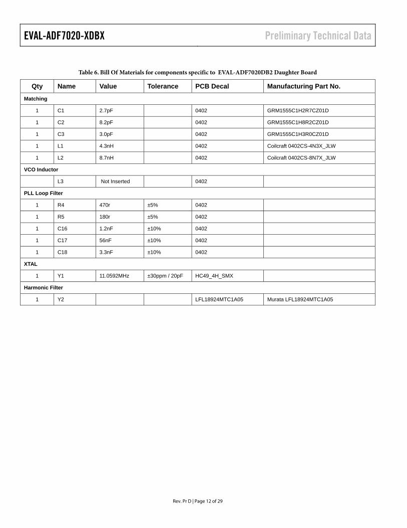
Table 6. Bill Of Materials for components specific to EVAL-ADF7020DB2 Daughter Board
Qty Name Value Tolerance PCB Decal Manufacturing Part No.
Matching
1 C1 2.7pF 0402 GRM1555C1H2R7CZ01D
1 C2 8.2pF 0402 GRM1555C1H8R2CZ01D
1 C3 3.0pF 0402 GRM1555C1H3R0CZ01D
1 L1 4.3nH 0402 Coilcraft 0402CS-4N3X_JLW
1 L2 8.7nH 0402 Coilcraft 0402CS-8N7X_JLW
VCO Inductor
L3 Not Inserted 0402
PLL Loop Filter
1 R4 470r ±5% 0402
1 R5 180r ±5% 0402
1 C16 1.2nF ±10% 0402
1 C17 56nF ±10% 0402
1 C18 3.3nF ±10% 0402
XTAL
1 Y1 11.0592MHz ±30ppm / 20pF HC49_4H_SMX
Harmonic Filter
1 Y2 LFL18924MTC1A05 Murata LFL18924MTC1A05
Preliminary Technical Data EVAL-ADF7020DBX
Rev. Pr D | Page 13 of 29
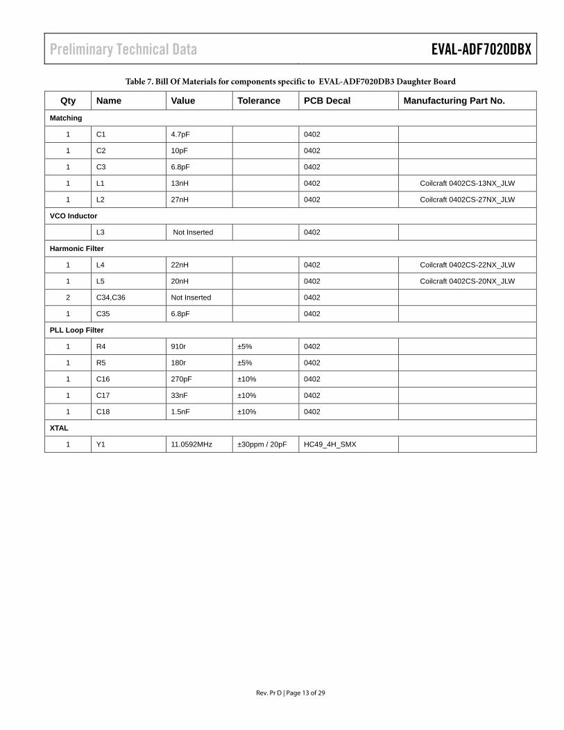
Table 7. Bill Of Materials for components specific to EVAL-ADF7020DB3 Daughter Board
Qty Name Value Tolerance PCB Decal Manufacturing Part No.
Matching
1 C1 4.7pF 0402
1 C2 10pF 0402
1 C3 6.8pF 0402
1 L1 13nH 0402 Coilcraft 0402CS-13NX_JLW
1 L2 27nH 0402 Coilcraft 0402CS-27NX_JLW
VCO Inductor
L3 Not Inserted 0402
Harmonic Filter
1 L4 22nH 0402 Coilcraft 0402CS-22NX_JLW
1 L5 20nH 0402 Coilcraft 0402CS-20NX_JLW
2 C34,C36 Not Inserted 0402
1 C35 6.8pF 0402
PLL Loop Filter
1 R4 910r ±5% 0402
1 R5 180r ±5% 0402
1 C16 270pF ±10% 0402
1 C17 33nF ±10% 0402
1 C18 1.5nF ±10% 0402
XTAL
1 Y1 11.0592MHz ±30ppm / 20pF HC49_4H_SMX

EVAL-ADF7020-XDBX Preliminary Technical Data
Rev. Pr D | Page 14 of 29
Table 8. Bill Of Materials for components specific to EVAL-ADF7020-1DB4 Daughter Board.
Qty Name Value Tolerance PCB Decal Manufacturing Part No.
Matching
1 C1 4.7pF 0402
1 C2 8.2pF 0402
1 C3 4.7pF 0402
1 L1 18nH 0402 Coilcraft 0402CS-18NX_JLW
1 L2 36nH 0402 Coilcraft 0402CS-36NX_JLW
VCO Tank Inductor
1 L3 6.2nH 2% 0402 Coilcraft 0402CS-6N2X_GLU
Harmonic Filter
1 L4 27nH 0402 Coilcraft 0402CS-27NX_JLW
1 L5 30nH 0402 Coilcraft 0402CS-30NX_JLW
1 C35 5.6pF 0402
2 C34,C36 Not Inserted 0402
Loop Filter
1 R4 1.2k ±5% 0402
1 R5 560r ±5% 0402
1 C16 390pF ±10% 0402
1 C17 15nF ±10% 0402
1 C18 1000pF ±10% 0402
1 Y1 11.0592MHz ±30ppm / 20pF HC49_4H_SMX
Preliminary Technical Data EVAL-ADF7020DBX
Rev. Pr D | Page 15 of 29
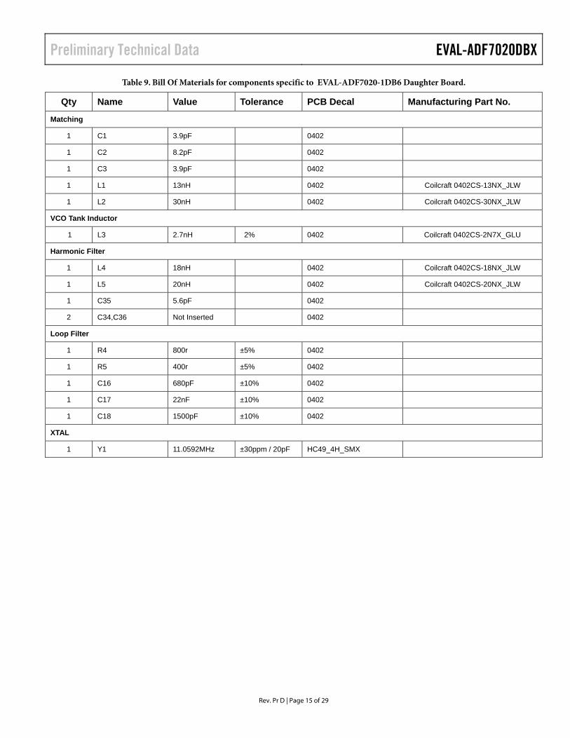
Table 9. Bill Of Materials for components specific to EVAL-ADF7020-1DB6 Daughter Board.
Qty Name Value Tolerance PCB Decal Manufacturing Part No.
Matching
1 C1 3.9pF 0402
1 C2 8.2pF 0402
1 C3 3.9pF 0402
1 L1 13nH 0402 Coilcraft 0402CS-13NX_JLW
1 L2 30nH 0402 Coilcraft 0402CS-30NX_JLW
VCO Tank Inductor
1 L3 2.7nH 2% 0402 Coilcraft 0402CS-2N7X_GLU
Harmonic Filter
1 L4 18nH 0402 Coilcraft 0402CS-18NX_JLW
1 L5 20nH 0402 Coilcraft 0402CS-20NX_JLW
1 C35 5.6pF 0402
2 C34,C36 Not Inserted 0402
Loop Filter
1 R4 800r ±5% 0402
1 R5 400r ±5% 0402
1 C16 680pF ±10% 0402
1 C17 22nF ±10% 0402
1 C18 1500pF ±10% 0402
XTAL
1 Y1 11.0592MHz ±30ppm / 20pF HC49_4H_SMX
EVAL-ADF7020-XDBX Preliminary Technical Data
Rev. Pr D | Page 16 of 29
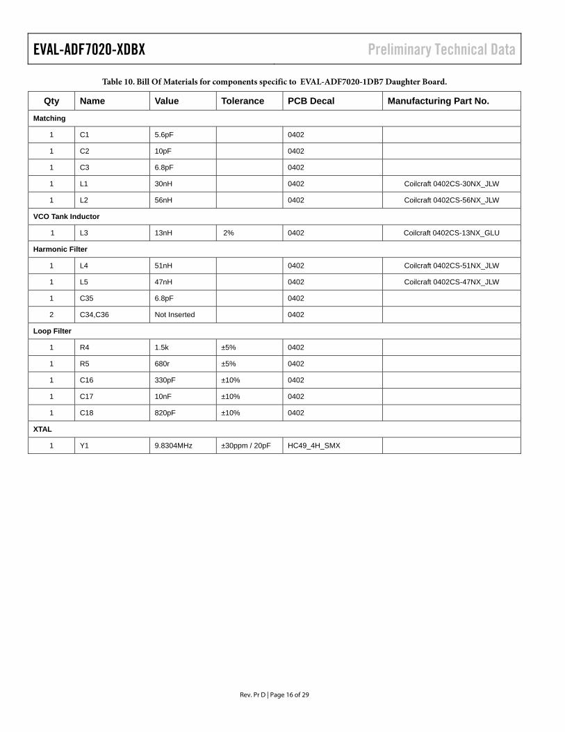
Table 10. Bill Of Materials for components specific to EVAL-ADF7020-1DB7 Daughter Board.
Qty Name Value Tolerance PCB Decal Manufacturing Part No.
Matching
1 C1 5.6pF 0402
1 C2 10pF 0402
1 C3 6.8pF 0402
1 L1 30nH 0402 Coilcraft 0402CS-30NX_JLW
1 L2 56nH 0402 Coilcraft 0402CS-56NX_JLW
VCO Tank Inductor
1 L3 13nH 2% 0402 Coilcraft 0402CS-13NX_GLU
Harmonic Filter
1 L4 51nH 0402 Coilcraft 0402CS-51NX_JLW
1 L5 47nH 0402 Coilcraft 0402CS-47NX_JLW
1 C35 6.8pF 0402
2 C34,C36 Not Inserted 0402
Loop Filter
1 R4 1.5k ±5% 0402
1 R5 680r ±5% 0402
1 C16 330pF ±10% 0402
1 C17 10nF ±10% 0402
1 C18 820pF ±10% 0402
XTAL
1 Y1 9.8304MHz ±30ppm / 20pF HC49_4H_SMX
Preliminary Technical Data EVAL-ADF7020DBX
Rev. Pr D | Page 17 of 29
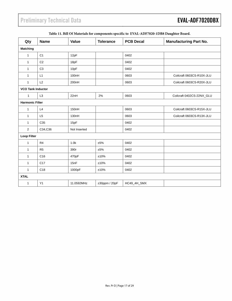
Table 11. Bill Of Materials for components specific to EVAL-ADF7020-1DB8 Daughter Board.
Qty Name Value Tolerance PCB Decal Manufacturing Part No.
Matching
1 C1 12pF 0402
1 C2 18pF 0402
1 C3 10pF 0402
1 L1 100nH 0603 Coilcraft 0603CS-R10X-JLU
1 L2 200nH 0603 Coilcraft 0603CS-R20X-JLU
VCO Tank Inductor
1 L3 22nH 2% 0603 Coilcraft 0402CS-22NX_GLU
Harmonic Filter
1 L4 150nH 0603 Coilcraft 0603CS-R15X-JLU
1 L5 130nH 0603 Coilcraft 0603CS-R13X-JLU
1 C35 15pF 0402
2 C34,C36 Not Inserted 0402
Loop Filter
1 R4 1.0k ±5% 0402
1 R5 390r ±5% 0402
1 C16 470pF ±10% 0402
1 C17 15nF ±10% 0402
1 C18 1000pF ±10% 0402
XTAL
1 Y1 11.0592MHz ±30ppm / 20pF HC49_4H_SMX

EVAL-ADF7020-XDBX Preliminary Technical Data
Rev. Pr D | Page 18 of 29
INSTALLING THE USB DRIVERS FOR THE EVAL-ADF70XXMBZ2 BOARD System Requirements
• Microsoft Windows 2000 or XP
• One available USB port (preferably USB2) Driver files The files required to install the UDB driver are:
• CyUSB.sys – the Cypress generic USB driver
• ADF70XXDK2.inf – the setup information file
• ADF70XXDK2.spt – the EZ-USB firmware (the last three digits of the filename represent the version)
Make sure you have these files available before plugging the board in for the first time.
Installing The software “ADF7xxx_ADIismLINK Install” should be downloaded from the CD or analog.com website and installed on your pc before plugging in the hardware. This zip file contains the relevant USB drivers and firmware necessary for operation of the EVAL-ADF70XXMBZ2 board. Note if you have installed ADIismLINK Rev1.0 previously you should run “purge_ADIismLINK.bat” to remove the old USB setup from the registry.
1. Windows 2000
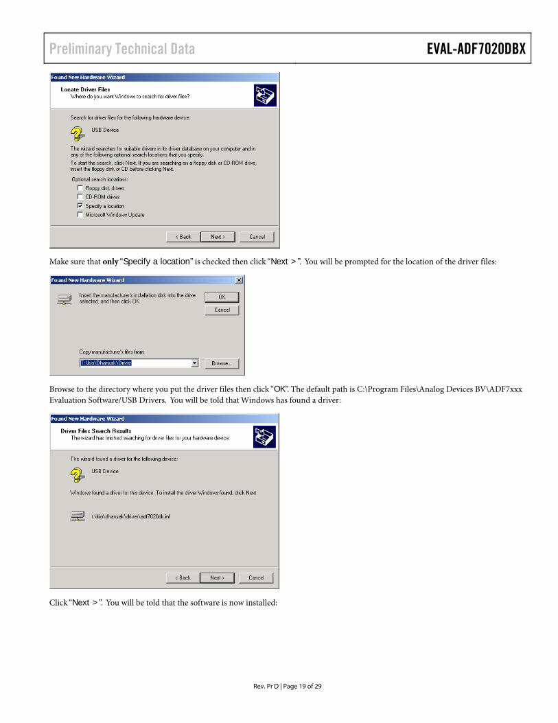
Plug in the ADF7020 development board, the “Found New Hardware Wizard” will appear after a while, click “Next >”:
Choose “Search for a suitable driver for my device (recommended)” and click “Next >”. You will be asked where Windows should look for the driver files:
Preliminary Technical Data EVAL-ADF7020DBX
Rev. Pr D | Page 19 of 29
Make sure that only “Specify a location” is checked then click “Next >”. You will be prompted for the location of the driver files:
Browse to the directory where you put the driver files then click “OK”. The default path is C:\Program Files\Analog Devices BV\ADF7xxx Evaluation Software/USB Drivers. You will be told that Windows has found a driver:
Click “Next >”. You will be told that the software is now installed:

EVAL-ADF7020-XDBX Preliminary Technical Data
Rev. Pr D | Page 20 of 29
Click “Finish”. The EZ-USB firmware will now be loaded and the development will appear as a new device, Windows should find the driver for it automatically.
2. Windows XP
Plug in the ADF7020 development board, the “Found New Hardware Wizard” will appear after a while:
Choose “Install from a list of specific location (Advanced)” and click “Next >”. You will be asked where Windows should look for the driver files:
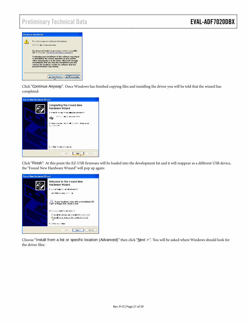
Choose “Search for the best driver in these locations”, make sure “Search removable media” is not selected and that “Include this location in the search” is selected. Browse to the directory where you put the driver files then click “Next >”. You will be informed that the driver has not passed Windows testing:
Preliminary Technical Data EVAL-ADF7020DBX
Rev. Pr D | Page 21 of 29
Click “Continue Anyway”. Once Windows has finished copying files and installing the driver you will be told that the wizard has completed:
Click “Finish”. At this point the EZ-USB firmware will be loaded into the development kit and it will reappear as a different USB device, the “Found New Hardware Wizard” will pop up again:
Choose “Install from a list or specific location (Advanced)” then click “Next >”. You will be asked where Windows should look for the driver files:

EVAL-ADF7020-XDBX Preliminary Technical Data
Rev. Pr D | Page 22 of 29
As before, choose “Search for the best driver in these locations” and “Include this location in the search”. Click “Next >”. You will be reminded that the driver has not passed Windows testing:
Click “Continue Anyway”. Once Windows has finished copying files and installing the driver you will be told that the wizard has completed:
Click “Finish”. You may be prompted to restart your computer:
If this appears you should restart the computer before trying to use any of the software that depends on the USB driver (ADF7020, ADF7012, ADF7025, ADF7021 .exes or ADF70xxHost).
Preliminary Technical Data EVAL-ADF7020DBX
Rev. Pr D | Page 23 of 29
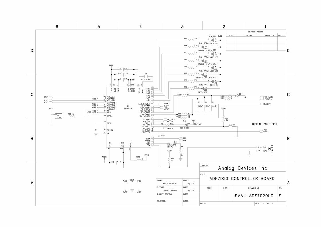
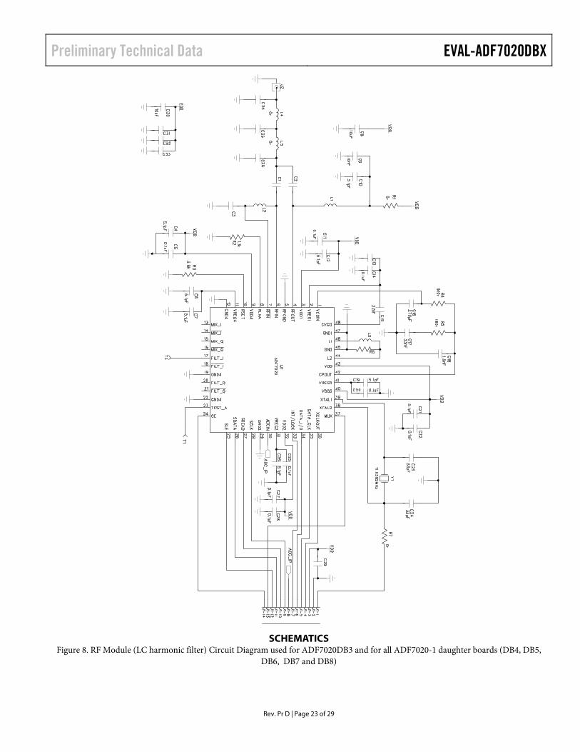
SCHEMATICS Figure 8. RF Module (LC harmonic filter) Circuit Diagram used for ADF7020DB3 and for all ADF7020-1 daughter boards (DB4, DB5,
DB6, DB7 and DB8)
EVAL-ADF7020-XDBX Preliminary Technical Data
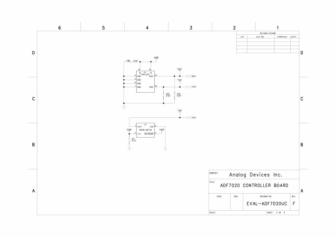
Rev. Pr D | Page 24 of 29
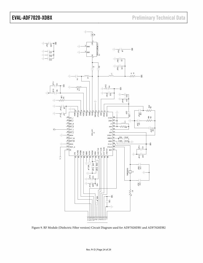
Figure 9. RF Module (Dielectric Filter version) Circuit Diagram used for ADF7020DB1 and ADF7020DB2