ad711 precision, low cost, high speed, bifet op amp …€¦ · precision, low cost, high speed,...
TRANSCRIPT

REV. E
Information furnished by Analog Devices is believed to be accurate andreliable. However, no responsibility is assumed by Analog Devices for itsuse, nor for any infringements of patents or other rights of third parties thatmay result from its use. No license is granted by implication or otherwiseunder any patent or patent rights of Analog Devices.
aAD711
One Technology Way, P.O. Box 9106, Norwood, MA 02062-9106, U.S.A.
Tel: 781/329-4700 www.analog.com
Fax: 781/326-8703 © Analog Devices, Inc., 2002
Precision, Low Cost,High Speed, BiFET Op Amp
FEATURES
Enhanced Replacement for LF411 and TL081
AC PERFORMANCE
Settles to �0.01% in 1.0 �s
16 V/�s min Slew Rate (AD711J)
3 MHz min Unity Gain Bandwidth (AD711J)
DC PERFORMANCE
0.25 mV max Offset Voltage: (AD711C)
3 �V/�C max Drift: (AD711C)
200 V/mV min Open-Loop Gain (AD711K)
4 �V p-p max Noise, 0.1 Hz to 10 Hz (AD711C)
Available in Plastic Mini-DIP, Plastic SOIC, Hermetic
Cerdip, and Hermetic Metal Can Packages
MIL-STD-883B Parts Available
Available in Tape and Reel in Accordance with
EIA-481A Standard
Surface Mount (SOIC)
Dual Version: AD712
PRODUCT DESCRIPTIONThe AD711 is a high speed, precision monolithic operationalamplifier offering high performance at very modest prices. Itsvery low offset voltage and offset voltage drift are the results ofadvanced laser wafer trimming technology. These performancebenefits allow the user to easily upgrade existing designs that useolder precision BiFETs and, in many cases, bipolar op amps.
The superior ac and dc performance of this op amp makes itsuitable for active filter applications. With a slew rate of 16 V/msand a settling time of 1 ms to ±0.01%, the AD711 is ideal as abuffer for 12-bit D/A and A/D Converters and as a high-speedintegrator. The settling time is unmatched by any similar ICamplifier.
The combination of excellent noise performance and low inputcurrent also make the AD711 useful for photo diode preamps.Common-mode rejection of 88 dB and open loop gain of400 V/mV ensure 12-bit performance even in high-speed unitygain buffer circuits.
The AD711 is pinned out in a standard op amp configurationand is available in seven performance grades. The AD711J andAD711K are rated over the commercial temperature range of0∞C to 70∞C. The AD711A, AD711B and AD711C are ratedover the industrial temperature range of –40∞C to +85∞C. TheAD711S and AD711T are rated over the military temperaturerange of –40∞C to +125∞C and are available processed to MIL-STD-883B, REV. E.
Extended reliability PLUS screening is available, specified overthe commercial and industrial temperature ranges. PLUSscreening includes 168 hour burn-in, as well as other environ-mental and physical tests.
The AD711 is available in an 8-pin plastic mini-DIP, smalloutline, cerdip, TO-99 metal can, or in chip form.
PRODUCT HIGHLIGHTS1. The AD711 offers excellent overall performance at very
competitive prices.
2. Analog Devices’ advanced processing technology and 100%testing guarantee a low input offset voltage (0.25 mV max,C grade, 2 mV max, J grade). Input offset voltage is specifiedin the warmed-up condition. Analog Devices’ laser waferdrift trimming process reduces input offset voltage drifts to3 mV/∞C max on the AD711C.
3. Along with precision dc performance, the AD711 offersexcellent dynamic response. It settles to ±0.01% in 1 ms andhas a 100% tested minimum slew rate of 16 V/ms. Thus thisdevice is ideal for applications such as DAC and ADCbuffers which require a combination of superior ac and dcperformance.
4. The AD711 has a guaranteed and tested maximum voltagenoise of 4 mV p-p, 0.1 to 10 Hz (AD711C).
5. Analog Devices’ well-matched, ion-implanted JFETs ensurea guaranteed input bias current (at either input) of 25 pAmax (AD711C) and an input offset current of 10 pA max(AD711C). Both input bias current and input offset currentare guaranteed in the warmed-up condition.
CONNECTION DIAGRAMS
10k�
VOS TRIM–15V
NCOFFSET
NULL
INVERTINGINPUT
NONINVERTING
INPUT
OFFSETNULL
OUTPUT
–VS
+VS
NC = NO CONNECT
AD711
NOTEPIN 4 CONNECTED TO CASE
8
7
6
5
1
2
3
4
NC = NO CONNECT
OFFSETNULL NC
OUTPUT
AD711
INVERTINGINPUT
NONINVERTINGINPUT
–VS
+VS
OFFSETNULL

REV. E–2–
AD711–SPECIFICATIONS (VS = �15 V @ TA = 25�C, unless otherwise noted.)
J/A/S K/B/T CParameter Min Typ Max Min Typ Max Min Typ Max Unit
INPUT OFFSET VOLTAGE1
Initial Offset 0.3 2/1/1 0.2 0.5 0.10 0.25 mVTMIN to TMAX 3/2/2 1.0 0.45 mVvs. Temp 7 20/20/20 5 10 2 5 mV/∞Cvs. Supply 76 95 80 100 86 110 dB
TMIN to TMAX 76/76/76 80 86 dBLong-Term Stability 15 15 15 mV/Month
INPUT BIAS CURRENT2
VCM = 0 V 15 50 15 50 15 25 pAVCM = 0 V @ TMAX 1.1/3.2/51 1.1/3.2/51 1.6 nAVCM = ±10 V 20 100 20 100 20 50 pA
INPUT OFFSET CURRENTVCM = 0 V 10 25 5 25 5 10 pAVCM = 0 V @ TMAX 0.6/1.6/26 0.6/1.6/26 0.65 nA
FREQUENCY RESPONSESmall Signal Bandwidth 3.0 4.0 3.4 4.0 3.4 4.0 MHzFull Power Response 200 200 200 kHzSlew Rate 16 20 18 20 18 20 V/msSettling Time to 0.01% 1.0 1.2 1.0 1.2 1.0 1.2 msTotal Harmonic Distortion 0.0003 0.0003 0.0003 %
INPUT IMPEDANCEDifferential 3 ¥ 1012�5.5 3 ¥ 1012�5.5 3 ¥ 1012�5.5 W�pFCommon Mode 3 ¥ 1012�5.5 3 ¥ 1012�5.5 3 ¥ 1012�5.5 W�pF
INPUT VOLTAGE RANGEDifferential3 ±20 ±20 ±20 VCommon-Mode Voltage4 +14.5, –11.5 +14.5, –11.5 +14.5, –11.5
TMIN to TMAX –VS + 4 +VS – 2 –VS + 4 +VS – 2 –VS + 4 +V – 2 VCommon-ModeRejection Ratio
VCM = ±10 V 76 88 80 88 86 94 dBTMIN to TMAX 76/76/76 84 80 84 86 90 dB
VCM = ±11 V 70 84 76 84 76 90 dBTMIN to TMAX 70/70/70 80 74 80 74 84 dB
INPUT VOLTAGE NOISE 2 2 2 4 mV p-p45 45 45 nV/÷Hz22 22 22 nV/÷Hz18 18 18 nV/÷Hz16 16 16 nV/÷Hz
INPUT CURRENT NOISE 0.01 0.01 0.01 pA/÷Hz
OPEN-LOOP GAIN 150 400 200 400 200 400 V/mV100/100/100 100 100 V/mV
OUTPUTCHARACTERISTICS
Voltage +13, –12.5 +13.9, –13.3 +13, –12.5 +13.9, –13.3 +13, –12.5 +13.9, –13.3 V±12/±12/±12 +13.8, –13.1 ±12 +13.8, –13.1 ±12 +13.8, –13.1 V
Current 25 25 25 mA
POWER SUPPLYRated Performance ±15 ±15 ±15 VOperating Range ±4.5 ±18 ±4.5 ±18 ±4.5 ±18 VQuiescent Current 2.5 3.4 2.5 3.0 2.5 2.8 mA
NOTES1Input Offset Voltage specifications are guaranteed after 5 minutes of operation at TA = 25∞C.2Bias Current specifications are guaranteed maximum at either input after 5 minutes of operation at TA = 25∞C. For higher temperatures, the current doubles every 10∞C.3Defined as voltage between inputs, such that neither exceeds ±10 V from ground.4Typically exceeding –14.1 V negative common-mode voltage on either input results in an output phase reversal.
Specifications subject to change without notice.
REV. E
AD711
–3–
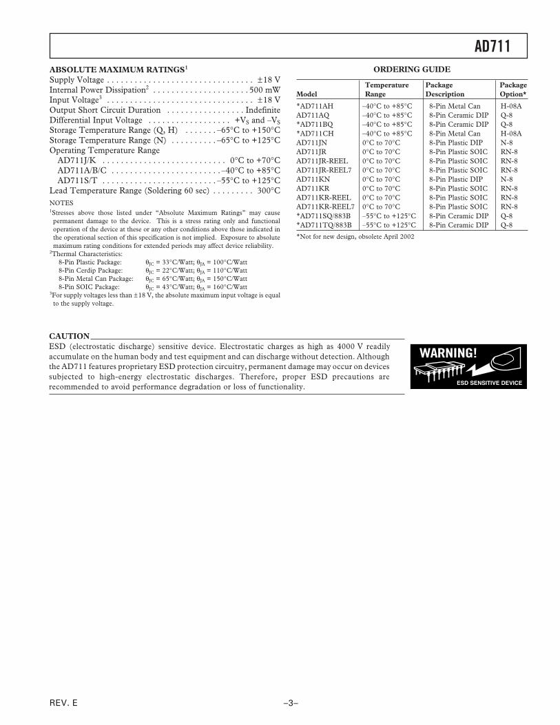
ABSOLUTE MAXIMUM RATINGS1
Supply Voltage . . . . . . . . . . . . . . . . . . . . . . . . . . . . . . . . ±18 VInternal Power Dissipation2 . . . . . . . . . . . . . . . . . . . . . 500 mWInput Voltage3 . . . . . . . . . . . . . . . . . . . . . . . . . . . . . . . . ±18 VOutput Short Circuit Duration . . . . . . . . . . . . . . . . . IndefiniteDifferential Input Voltage . . . . . . . . . . . . . . . . . . +VS and –VS
Storage Temperature Range (Q, H) . . . . . . . –65∞C to +150∞CStorage Temperature Range (N) . . . . . . . . . . –65∞C to +125∞COperating Temperature Range
AD711J/K . . . . . . . . . . . . . . . . . . . . . . . . . . . 0∞C to +70∞CAD711A/B/C . . . . . . . . . . . . . . . . . . . . . . . . –40∞C to +85∞CAD711S/T . . . . . . . . . . . . . . . . . . . . . . . . . –55∞C to +125∞C
Lead Temperature Range (Soldering 60 sec) . . . . . . . . . 300∞CNOTES1Stresses above those listed under “Absolute Maximum Ratings” may cause
permanent damage to the device. This is a stress rating only and functionaloperation of the device at these or any other conditions above those indicated inthe operational section of this specification is not implied. Exposure to absolutemaximum rating conditions for extended periods may affect device reliability.
2Thermal Characteristics:8-Pin Plastic Package: qJC = 33∞C/Watt; qJA = 100∞C/Watt8-Pin Cerdip Package: qJC = 22∞C/Watt; qJA = 110∞C/Watt8-Pin Metal Can Package: qJC = 65∞C/Watt; qJA = 150∞C/Watt8-Pin SOIC Package: qJC = 43∞C/Watt; qJA = 160∞C/Watt
3For supply voltages less than ±18 V, the absolute maximum input voltage is equalto the supply voltage.
ORDERING GUIDE
Temperature Package PackageModel Range Description Option*
*AD711AH –40∞C to +85∞C 8-Pin Metal Can H-08AAD711AQ –40∞C to +85∞C 8-Pin Ceramic DIP Q-8*AD711BQ –40∞C to +85∞C 8-Pin Ceramic DIP Q-8*AD711CH –40∞C to +85∞C 8-Pin Metal Can H-08AAD711JN 0∞C to 70∞C 8-Pin Plastic DIP N-8AD711JR 0∞C to 70∞C 8-Pin Plastic SOIC RN-8AD711JR-REEL 0∞C to 70∞C 8-Pin Plastic SOIC RN-8AD711JR-REEL7 0∞C to 70∞C 8-Pin Plastic SOIC RN-8AD711KN 0∞C to 70∞C 8-Pin Plastic DIP N-8AD711KR 0∞C to 70∞C 8-Pin Plastic SOIC RN-8AD711KR-REEL 0∞C to 70∞C 8-Pin Plastic SOIC RN-8AD711KR-REEL7 0∞C to 70∞C 8-Pin Plastic SOIC RN-8*AD711SQ/883B –55∞C to +125∞C 8-Pin Ceramic DIP Q-8*AD711TQ/883B –55∞C to +125∞C 8-Pin Ceramic DIP Q-8
*Not for new design, obsolete April 2002
WARNING!
ESD SENSITIVE DEVICE
CAUTIONESD (electrostatic discharge) sensitive device. Electrostatic charges as high as 4000 V readilyaccumulate on the human body and test equipment and can discharge without detection. Althoughthe AD711 features proprietary ESD protection circuitry, permanent damage may occur on devicessubjected to high-energy electrostatic discharges. Therefore, proper ESD precautions arerecommended to avoid performance degradation or loss of functionality.

REV. E
AD711–Typical Performance Characteristics
–4–
SUPPLY VOLTAGE – �Volts
OU
TP
UT
VO
LTA
GE
SW
ING
– V
olt
s
00 5 10
10
5
15
20
15 20
RL = 2k�
25�C
+VOUT
–VOUT
TPC 2. Output Voltage Swing vs.Supply Voltage
TEMPERATURE – C
INP
UT
BIA
S C
UR
RE
NT
(V
CM
= 0
) –
Am
ps
10–12
–60 –40 –20 0 20 40 60 80 100 120 140
10–11
10–10
10–9
10–8
10–7
10–6
TPC 5. Input Bias Current vs. Tem-perature
AMBIENT TEMPERATURE – C
SH
OR
T C
IRC
UIT
CU
RR
EN
T L
IMIT
– m
A
–6010
–40 –20 0 20 40 60 80 100 120 140
12
14
16
18
20
22
24
26
–OUTPUT CURRENT
+OUTPUT CURRENT
TPC 8. Short Circuit Current Limitvs. Temperature
SUPPLY VOLTAGE – �Volts
INP
UT
VO
LTA
GE
SW
ING
– V
olt
s
00 5 10
10
5
15
20
15 20
RL = 2k�
25�C
TPC 1. Input Voltage Swing vs.Supply Voltage
SUPPLY VOLTAGE – �Volts
QU
IES
CE
NT
CU
RR
EN
T –
mA
1.750 5 10 15 20
2.00
2.25
2.50
2.75
TPC 4. Quiescent Current vs. Sup-ply Voltage
COMMON MODE VOLTAGE – Volts
INP
UT
BIA
S C
UR
RE
NT
– p
A
0–10
50
25
75
100
MAX J GRADE LIMIT
–5 0 5 10
VS = �15V25�C
TPC 7. Input Bias Current vs. Com-mon Mode Voltage
LOAD RESISTANCE – �
OU
TP
UT
VO
LTA
GE
SW
ING
– V
olt
s p
-p
010
15
100 1k 10k
20
25
30
10
5
�15V SUPPLIES
TPC 3. Output Voltage Swing vs.Load Resistance
FREQUENCY – Hz
OU
TP
UT
IMP
ED
AN
CE
– �
0.011k
AVCL = 1
10k 100k 1M 10M
0.01
1
10
100
TPC 6. Output Impedance vs. Fre-quency
TEMPERATURE – C
UN
ITY
GA
IN B
AN
DW
IDT
HT
– M
Hz
–603.0
–40 –20 0 20 40 60 80 100 120 140
3.5
4.0
4.5
5.0
TPC 9. Unity Gain Bandwidth vs.Temperature

REV. E –5–
AD711
SUPPLY MODULATION FREQUENCY – Hz
PO
WE
R S
UP
PLY
RE
JEC
TIO
N –
dB
010
20
40
60
80
100
110
100 1k 10k 10k1
–SUPPLY
+SUPPLY
VS = �15 SUPPLIESWITH 1V p-p SINEWAVE 25 C
TPC 12. Power Supply Rejectionvs. Frequency
SETTLING TIME – �s
OU
TP
UT
SW
ING
FR
IM 0
V T
O �
Volt
s0.5
–10
–8
–6
–4
–2
0
2
2
4
6
8
0.6 0.7 0.8 0.9 1.0
ERROR 1% 0.1% 0.01%
1% 0.1% 0.01%
TPC 15. Output Swing and Errorvs. Settling Time
INPUT ERROR SIGNAL – mV(AT SUMMING JUNCTION)
SL
EW
RA
TE
– V
��s
00
100 200 300 400
5
10
15
20
25
500 600 700 800 900
TPC 18. Slew Rate vs. InputError Signal
SUPPLY VOLTAGE – �Volts
OP
EN
-LO
OP
GA
IN –
dB
095
5 10 15 20
100
105
110
115
120
125RL = 2k�
25�C
TPC 11. Open-Loop Gain vs.Supply Voltage
INPUT FREQUENCY – Hz
0
5
10
30
10M100k 1M
15
20
25
OU
TP
UT
VO
LTA
GE
– V
olt
s p
-p
RL = 2k�
25 CVS = �15V
TPC 14. Large Signal FrequencyResponse
FREQUENCY – Hz
11
10
10
INP
UT
NO
ISE
VO
LTA
GE
– n
V/
Hz
100
1k
100 1k 10k 100k
TPC 17. Input Noise VoltageSpectral Density
FREQUENCY – Hz
OP
EN
LO
OP
GA
IN –
dB
10–20
100 1k 10k 100k 1M
0
20
40
60
10M
80
100
GAIN
RL = 2k�
C = 100pF
PHASE
–20
0
20
40
60
80
100
PH
AS
E M
AR
GIN
– D
egre
es
TPC 10. Open-Loop Gain andPhase Margin vs. Frequency
FREQUENCY – Hz
CM
R –
dB
100
010
20
100
VS = �15VVCM = 1V p-p 25 C
40
60
80
1k 10k 100k 1M
TPC 13. Common Mode Rejectionvs. Frequency
FREQUENCY – Hz
TH
D –
dB
–130100
–120
–110
–100
–90
–80
–70
1k 10k 100k
3V RMSRL = 2k�
CL = 100pF
TPC 16. Total Harmonic Distor-tion vs. Frequency

REV. E
AD711
–6–
TPC 21. Offset Null Configurations
TPC 22c. Unity Gain FollowerPulse Response (Small Signal)
TPC 23c. Unity Gain Inverter PulseResponse (Small Signal)
TPC 20. T.H.D. Test Circuit
TPC 22b. Unity Gain FollowerPulse Response (Large Signal)
TPC 23b. Unity Gain InverterPulse Response (Large Signal)
TEMPERATURE – C
SL
EW
RA
TE
– V
/�s
–60 –40 –20 0 20 40 60 80 100 120 140
20
25
15
16
17
18
19
21
22
23
24
TPC 19. Slew Rate vs. Temperature
RL2k�
VOUTVIN
+VS
–VS
0.1�F
CL100pF
0.1�F
SQUARE WAVEINPUT
AD711
TPC 22a. Unity Gain Follower
RL2k�
VOUT
VIN
+VS
–VS
0.1�F
CL100pF
0.1�F
SQUARE WAVEINPUT
5k�
AD711
5k�
TPC 23a. Unity Gain Inverter
2k�
OUTPUT
+VS
–VS
0.1�F
100pF0.1�F
AD711INPUT
+VS
–VS
0.1�F
AD711
10k�
0.1�F 1.3Mk�
+VS
–VS
0.1�F
AD711
10k�
0.1�F

REV. E
AD711
–7–
OPTIMIZING SETTLING TIMEMost bipolar high-speed D/A converters have current outputs;therefore, for most applications, an external op amp is requiredfor current-to-voltage conversion. The settling time of theconverter/op amp combination depends on the settling time ofthe DAC and output amplifier. A good approximation is:
tS Total = (tS DAC )2 + (tS AMP )2 (1)
The settling time of an op amp DAC buffer will vary with thenoise gain of the circuit, the DAC output capacitance, and withthe amount of external compensation capacitance across theDAC output scaling resistor.
Settling time for a bipolar DAC is typically 100 ns to 500 ns.Previously, conventional op amps have required much longersettling times than have typical state-of-the-art DACs; therefore,the amplifier settling time has been the major limitation to ahigh-speed voltage-output D-to-A function. The introductionof the AD711/712 family of op amps with their 1 ms (to ±0.01%of final value) settling time now permits the full high-speedcapabilities of most modern DACs to be realized.
In addition to a significant improvement in settling time, thelow offset voltage, low offset voltage drift, and high open-loopgain of the AD711 family assures 12-bit accuracy over the fulloperating temperature range.
The excellent high-speed performance of the AD711 is shownin the oscilloscope photos of Figure 2. Measurements were takenusing a low input capacitance amplifier connected directly to thesumming junction of the AD711 – both photos show the worstcase situation: a full-scale input transition. The DAC’s 4 kW[10 kW�8 kW = 4.4 kW] output impedance together with a 10 kWfeedback resistor produce an op amp noise gain of 3.25. Thecurrent output from the DAC produces a 10 V step at the opamp output (0 to –10 V Figure 2a, –10 V to 0 V Figure 2b.)
Therefore, with an ideal op amp, settling to ±1/2 LSB (±0.01%)requires that 375 mV or less appears at the summing junction.This means that the error between the input and output (thatvoltage which appears at the AD711 summing junction) mustbe less than 375 mV. As shown in Figure 2, the total settling timefor the AD711/AD565 combination is 1.2 microseconds.
OUTPUT–10V TO +10V
+15V0.1�F
10pF
0.1�F
AD711K
DACIOUT = 4 �IREF � CODE
0.5mA
IREF
20k�
19.95k�
R1100�
BIPOLAROFFSET ADJUST
IO
DACOUT
10VSPAN
–15V
20VSPAN
5k�
5k�
5k�
10V
MSB LSB
REFOUT VCC
REFIN
REFGND
R2100�GAIN
ADJUST
0.1�F
AD565A
BIPOLAROFF
9.95k�
–VEE0.1�F
POWERGND
Figure 1. ±10 V Voltage Output Bipolar DAC
Figure 2. Settling Characteristics for AD711 with AD565A
a. (Full-Scale Negative Transition) b. (Full-Scale Positive Transition)

REV. E
AD711
–8–
OP AMP SETTLING TIME—A MATHEMATICAL MODELThe design of the AD711 gives careful attention to optimizingindividual circuit components; in addition, a careful tradeoff wasmade: the gain bandwidth product (4 MHz) and slew rate(20 V/ms) were chosen to be high enough to provide very fastsettling time but not too high to cause a significant reduction inphase margin (and therefore stability). Thus designed, the AD711settles to ±0.01%, with a 10 V output step, in under 1 ms, whileretaining the ability to drive a 100 pF load capacitance whenoperating as a unity gain follower.
If an op amp is modeled as an ideal integrator with a unity gaincrossover frequency of wo/2p, Equation 1 will accurately describethe small signal behavior of the circuit of Figure 3a, consisting ofan op amp connected as an I-to-V converter at the output of abipolar or CMOS DAC. This equation would completely describethe output of the system if not for the op amp’s finite slew rateand other nonlinear effects.
VO
IIN= –R
R(Cf = CX )wo
s2 + GN
wo+ RCf
ÊËÁ
ˆ¯̃s +1 (3)
where:
wo2p
=op amp’s unity gain frequency
GN = “noise” gain of circuit
1+ RRO
ÊËÁ
ˆ¯̃
This equation may then be solved for Cf:
Cf = 2 -GN
Rwo+
2 RCXwo + (1-GN )Rwo
(3)
In these equations, capacitor CX is the total capacitor appearingthe inverting terminal of the op amp. When modeling a DACbuffer application, the Norton equivalent circuit of Figure 3acan be used directly; capacitance CX is the total capacitance ofthe output of the DAC plus the input capacitance of the op amp(since the two are in parallel).
AD711
CXROIO
CF
R
RL CL
VOUT
Figure 3a. Simplified Model of the AD711 Used as aCurrent-Out DAC Buffer
When RO and IO are replaced with their Thevenin VIN and RIN
equivalents, the general purpose inverting amplifier of Figure 26bis created. Note that when using this general model, capacitanceCX is either the input capacitance of the op amp if a simple inverting
op amp is being simulated or it is the combined capacitance ofthe DAC output and the op amp input if the DAC buffer isbeing modeled.
AD711
CX
RIN
CF
R
RL CL
VOUT
VIN
Figure 3b. Simplified Model of the AD711Used as an Inverter
In either case, the capacitance CX causes the system to go froma one-pole to a two-pole response; this additional pole increasessettling time by introducing peaking or ringing in the op ampoutput. Since the value of CX can be estimated with reasonableaccuracy, Equation 2 can be used to choose a small capacitor,CF, to cancel the input pole and optimize amplifier response.Figure 4 is a graphical solution of Equation 2 for the AD711with R = 4 kW.
CF
00 10
CX
10
20
30
40
50
60
20 30 40 50 60
GN = 4.0
GN = 1.0
GN = 1.5
GN = 2.0
GN = 3.0
Figure 4. Value of Capacitor CF vs. Value of CX
The photos of Figures 5a and 5b show the dynamic response ofthe AD711 in the settling test circuit of Figure 6.
The input of the settling time fixture is driven by a flat-top pulsegenerator. The error signal output from the false summing nodeof A1 is clamped, amplified by A2 and then clamped again. Theerror signal is thus clamped twice: once to prevent overloadingamplifier A2 and then a second time to avoid overloading theoscilloscope preamp. The Tektronix oscilloscope preamp type7A26 was carefully chosen because it does not overload withthese input levels. Amplifier A2 needs to be a very high speedFET-input op amp; it provides a gain of 10, amplifying the errorsignal output of A1.

REV. E
AD711
–9–
Figure 5a. Settling Characteristics 0 to +10 V StepUpper Trace: Output of AD711 Under Test (5 V/Div)Lower Trace: Amplified Error Voltage (0.01%/Div)
Figure 5b. Settling Characteristics 0 to –10 V StepUpper Trace: Output of AD711 Under Test (5 V/Div)Lower Trace: Amplified Error Voltage (0.01%/Div)
GUARDINGThe low input bias current (15 pA) and low noise characteristicsof the AD711 BiFET op amp make it suitable for electrometerapplications such as photo diode preamplifiers and picoampere
5pF
AD3554
VERROR � 5
+15V
5k�
–15V
0.47�F
HP2835
TEXTRONIX 7A26OSCILLOSCOPE
PREAMPINPUT SELECTION
1M� 20pF
0.1�F
AD711
+15V–15V
0.1�F
VOUT
10pF
HP2835
10k�
0.2-0.0pF
1.1k�10k�
5-18pF
10k�
200k�
4.99k� 4.99k�
VIN
DATADYNAMICS
5109
(OREQUIVALENTFLAT TOPPULSEGENERATOR)
0.47�F
205�
Figure 6. Settling Time Test Circuit
current-to-voltage converters. The use of a guarding techniquesuch as that shown in Figure 7, in printed circuit board layoutand construction is critical to minimize leakage currents. Theguard ring is connected to a low impedance potential at thesame level as the inputs. High impedance signal lines shouldnot be extended for any unnecessary length on the printedcircuit board.
1
8
7
6
5
4
3
2 6
5
7
8
23
1
4
Figure 7. Board Layout for Guarding Inputs
D/A CONVERTER APPLICATIONSThe AD711 is an excellent output amplifier for CMOS DACs.It can be used to perform both 2-quadrant and 4-quadrantoperation. The output impedance of a DAC using an invertedR-2R ladder approaches R for codes containing many 1s, 3Rfor codes containing a single 1, and for codes containing allzero, the output impedance is infinite.
For example, the output resistance of the AD7545 will modu-late between 11 kW and 33 kW. Therefore, with the DAC’sinternal feedback resistance of 11 kW, the noise gain will varyfrom 2 to 4/3. This changing noise gain modulates the effect ofthe input offset voltage of the amplifier, resulting in nonlinearDAC amplifier performance.
The AD711K with guaranteed 500 mV offset voltage minimizesthis effect to achieve 12-bit performance.

REV. E
AD711
–10–
AD711K
CF
VOUT
0.1�F
0.1�F
–15
+15C1
33pF
R2*
OUT1RFBVDD
VREF
DGND AGNDR1*
VIN
ANALOGCOMMON
GAINADJUST
DB11-DB0
VDD
AD7545
*FOR VALUES R1 AND R2,REFER TO TABLE 1
Figure 8. Unipolar Binary Operation
R1 and R2 calibrate the zero offset and gain error of the DAC.Specific values for these resistors depend upon the grade ofAD7545 and are shown below.
Table I. Recommended Trim Resistor Values vs. Gradesof the AD7545 for VDD = 5 V
TRIMRESISTOR JN/AQ/SD KN/BQ/TD LN/CQ/UD GLN/GCQ/GUD
R1 500 W 200 W 100 W 20 WR2 150 W 68 W 33 W 6.8 W
NOISE CHARACTERISTICSThe random nature of noise, particularly in the 1/f region, makesit difficult to specify in practical terms. At the same time,designers of precision instrumentation require certain guaranteedmaximum noise levels to realize the full accuracy of their equipment.
The AD711C grade is specified at a maximum level of 4.0 mV p-p,in a 0.1 Hz to 10 Hz bandwidth. Each AD711C receives a 100%noise test for two 10-second intervals; devices with any excursionin excess of 4.0 mV are rejected. The screened lot is then submittedto Quality Control for verification on an AQL basis.
All other grades of the AD711 are sample-tested on an AQLbasis to a limit of 6 mV p-p, 0.1 to 10 Hz.
DRIVING THE ANALOG INPUT OF AN A/D CONVERTERAn op amp driving the analog input of an A/D converter, suchas that shown in Figure 11, must be capable of maintaining aconstant output voltage under dynamically changing load conditions.In successive-approximation converters, the input current is
compared to a series of switched trial currents. The comparisonpoint is diode clamped but may deviate several hundred millivoltsresulting in high frequency modulation of A/D input current.
Figures 10a and 10b show the settling time characteristics of theAD711 when used as a DAC output buffer for the AD7545.
a. Full-Scale Positive b. Full-Scale NegativeTransition Transition
Figure 10. Settling Characteristics for AD711 with AD7545
compared to a series of switched trial currents. The comparisonpoint is diode clamped but may deviate several hundred milli-volts resulting in high frequency modulation of A/D inputcurrent. The output impedance of a feedback amplifier is madeartificially low by the loop gain. At high frequencies, where theloop gain is low, the amplifier output impedance can approachits open loop value. Most IC amplifiers exhibit a minimum openloop output impedance of 25 W due to current limiting resistors.A few hundred microamps reflected from the change in con-verter loading can introduce errors in instantaneous input
Figures 8 and 9 show the AD711 and AD7545 (12-bit CMOSDAC) configured for unipolar binary (2-quadrant multiplication)or bipolar (4-quadrant multiplication) operation. Capacitor C1provides phase compensation to reduce overshoot and ringing.
+15V0.1�F
0.1�F
AD711K
–15V
R310k�1%
+15V0.1�F
0.1�F
AD711K
–15V
R520k�1%
R420k�
1%R2*
C133pF
OUT1RFBVDD
VREF
DGNDAGNDR1*
VIN
GAINADJUST
DB11-DB0
VDD
VOUT
AD7545
12
DATA INPUT ANALOGCOMMON
*FOR VALUES R1 AND R2,REFER TO TABLE 1
Figure 9. Bipolar Operation
+15V0.1�F
0.1�F
AD711
–15V
R2100�
GAINADJUST
12/8
R1100�
OFFSETADJUST
CS
AO
R/C
CE
REF IN
REF OUT
BIP OFF
10VIN
20VIN
ANA COM
STS
HIGHBITS
MIDDLEBITS
LOWBITS
+5V
+15V
–15V
DIG COM
AD574
�10VANALOG
INPUT
ANALOG COM
Figure 11. AD711 as ADC Unity Gain Buffer

REV. E
AD711
–11–
DRIVING A LARGE CAPACITIVE LOADThe circuit in Figure 13 employs a 100 W isolation resistor whichenables the amplifier to drive capacitive loads exceeding 1500 pF;the resistor effectively isolates the high frequency feedback fromthe load and stabilizes the circuit. Low frequency feedback isreturned to the amplifier summing junction via the low passfilter formed by the 100 W series resistor and the load capaci-tance, CL. Figure 14 shows a typical transient response forthis connection.
RL
INPUT
+VS
–VS
0.1�F
CL0.1�FTYPICAL CAPACITANCE
LIMIT FOR VARIOUSLOAD RESISTORS
RL CL UP TO2k� 1500pF10k� 1500pF20k� 1000pF
4.99k� AD711100�
30pF
4.99k�
OUTPUT
Figure 13. Circuit for Driving a Large Capacitive Load
Figure 14. Transient Response RL = 2 kW, CL = 500 pF
ACTIVE FILTER APPLICATIONSIn active filter applications using op amps, the dc accuracy of theamplifier is critical to optimal filter performance. The amplifier’soffset voltage and bias current contribute to output error. Offsetvoltage will be passed by the filter and may be amplified to produceexcessive output offset. For low frequency applications requiring
large value input resistors, bias currents flowing through theseresistors will also generate an offset voltage.
In addition, at higher frequencies, an op amp’s dynamics mustbe carefully considered. Here, slew rate, bandwidth, and open-loopgain play a major role in op amp selection. The slew rate mustbe fast as well as symmetrical to minimize distortion. The amplifier’sbandwidth in conjunction with the filter’s gain will dictate thefrequency response of the filter.
The use of a high performance amplifier such a s the AD711will minimize both dc and ac errors in all active filter applica-tions.
SECOND ORDER LOW PASS FILTERFigure 15 depicts the AD711 configured as a second orderButterworth low pass filter. With the values as shown, the cornerfrequency will be 20 kHz; however, the wide bandwidth of theAD711 permits a corner frequency as high as several hundredkilohertz. Equations for component selection are shown below.
R1 = R2 = user selected (typical values: 10 kW – 100 kW) (4)
C1=
1.414(2 p)( f cutoff )(R1)
, C2 =0.707
(2 p)( f cutoff )(R1) (5)
Where:
C1 and C2 are in farads.
VOUT
+15V
–15V
0.1�F
0.1�F
AD711VINC2
280pF
R220k�
R120k�
C1560pF
Figure 15. Second Order Low Pass Filter
An important property of filters is their out-of-band rejection.The simple 20 kHz low pass filter shown in Figure 15, might beused to condition a signal contaminated with clock pulses orsampling glitches which have considerable energy content athigh frequencies.
The low output impedance and high bandwidth of the AD711minimize high frequency feedthrough as shown in Figure 16.
The upper trace is that of another low-cost BiFET op ampshowing 17 dB more feedthrough at 5 MHz.
Figure 16.
voltage. If the A/D conversion speed is not excessive and thebandwidth of the amplifier is sufficient, the amplifier’s outputwill return to the nominal value before the converter makes itscomparison. However, many amplifiers have relatively narrowbandwidth yielding slow recovery from output transients. TheAD711 is ideally suited to drive high speed A/D converters sinceit offers both wide bandwidth and high open-loop gain.
a. Source Current = 2 mA b. Sink Current = 1 mA
Figure 12. ADC Input Unity Gain Buffer Recovery Times

REV. E
AD711
–12–
+15V
–15V
0.1�F
0.1�F
A1AD711
VIN
VOUT
+15V
–15V
0.1�F
0.1�F
A2AD711
A
*
B
*
C
*
D
*
0.001�F
4.9395E–15 5.9276E–15 5.9276E–15 4.9395E–15
2800� 6190� 6490� 6190�
0.001�F100k�
124k�
2800�
*SEE TEXT4.99k�
4.99k�
Figure 17. 9-Pole Chebychev Filter
+15V
–15V
0.1�F
0.1�F
1/2AD712
1/2AD712 0.001�F
0.001�F
R
1k�
4.99k�R: 24.9k� FOR 4.9395E–15
29.4k� FOR 5.9276E–15
Figure 18. FDNR for 9-Pole Chebychev Filter Figure 19. High Frequency Response for 9-PoleChebychev Filter
9-POLE CHEBYCHEV FILTERFigure 17 shows the AD711 and its dual counterpart, the AD712,as a 9-pole Chebychev filter using active frequency dependentnegative resistors (FDNR). With a cutoff frequency of 50 kHzand better than 90 dB rejection, it may be used as an anti-aliasingfilter for a 12-bit data acquisition system with 100 kHz throughput.
As shown in Figure 17, the filter is comprised of four FDNRs (A,B, C, D) having values of 4.9395 � 10–15 and 5.9276 �10–15 farad-seconds. Each FDNR active network provides a
2-pole response; for a total of 8 poles. The 9th pole consists of a0.001 mF capacitor and a 124 kW resistor at Pin 3 of amplifier A2.Figure 18 depicts the circuits for each FDNR with the properselection of R. To achieve optimal performance, the 0.001 mFcapacitors must be selected for 1% or better matching and allresistors should have 1% or better tolerance.

REV. E
AD711
–13–
OUTLINE DIMENSIONS
8-Lead Metal Can [TO-99](H-8)
Dimensions shown in inches and (millimeters)
0.2500 (6.35) MIN
0.5000 (12.70)MIN0.1850 (4.70)
0.1650 (4.19)
REFERENCE PLANE
0.0500 (1.27) MAX
0.0190 (0.48)0.0160 (0.41)
0.0210 (0.53)0.0160 (0.41)0.0400 (1.02)
0.0100 (0.25)
0.0400 (1.02) MAX
BASE & SEATING PLANE
0.0340 (0.86)0.0280 (0.71)
0.0450 (1.14)0.0270 (0.69)
0.1600 (4.06)0.1400 (3.56)
0.1000 (2.54) BSC
6
2 8
7
5
4
3
1
0.2000(5.08)BSC
0.1000(2.54)BSC
45 BSC
0.37
00 (
9.40
)0.
3350
(8.
51)
0.33
50 (
8.51
)0.
3050
(7.
75)
CONTROLLING DIMENSIONS ARE IN INCHES; MILLIMETERS DIMENSIONS(IN PARENTHESES) ARE ROUNDED-OFF EQUIVALENTS FORREFERENCE ONLY AND ARE NOT APPROPRIATE FOR USE IN DESIGN
COMPLIANT TO JEDEC STANDARDS MO-002AK
8-Lead Ceramic Dip – Glass Hermetic Seal [CERDIP](Q-8)
Dimensions shown in inches and (millimeters)
1 4
8 5
0.310 (7.87)0.220 (5.59)PIN 1
0.005 (0.13)MIN
0.055 (1.40)MAX
0.100 (2.54) BSC
15 0
0.320 (8.13)0.290 (7.37)
0.015 (0.38)0.008 (0.20)
SEATINGPLANE
0.200 (5.08)MAX
0.405 (10.29) MAX
0.150 (3.81)MIN
0.200 (5.08)0.125 (3.18)
0.023 (0.58)0.014 (0.36)
0.070 (1.78)0.030 (0.76)
0.060 (1.52)0.015 (0.38)
CONTROLLING DIMENSIONS ARE IN INCH; MILLIMETERS DIMENSIONS(IN PARENTHESES) ARE ROUNDED-OFF MILLIMETER EQUIVALENTS FORREFERENCE ONLY AND ARE NOT APPROPRIATE FOR USE IN DESIGN
8-Lead Plastic Dual-in-Line Package [PDIP](N-8)
Dimensions shown in inches and (millimeters)
SEATINGPLANE
0.015(0.38)MIN
0.180(4.57)MAX
0.150 (3.81)0.130 (3.30)0.110 (2.79) 0.060 (1.52)
0.050 (1.27)0.045 (1.14)
8
1 4
5 0.295 (7.49)0.285 (7.24)0.275 (6.98)
0.100 (2.54)BSC
0.375 (9.53)0.365 (9.27)0.355 (9.02)
0.150 (3.81)0.135 (3.43)0.120 (3.05)
0.015 (0.38)0.010 (0.25)0.008 (0.20)
0.325 (8.26)0.310 (7.87)0.300 (7.62)
0.022 (0.56)0.018 (0.46)0.014 (0.36)
CONTROLLING DIMENSIONS ARE IN INCHES; MILLIMETERS DIMENSIONS(IN PARENTHESES)
COMPLIANT TO JEDEC STANDARDS MO-095AA
8-Lead Standard Small Outline Package [SOIC]Narrow Body
(RN-8)Dimensions shown in millimeters and (inches)
0.25 (0.0098)0.19 (0.0075)
1.27 (0.0500)0.41 (0.0160)
0.50 (0.0196)0.25 (0.0099)
� 45�
8�0�
1.75 (0.0688)1.35 (0.0532)
SEATINGPLANE
0.25 (0.0098)0.10 (0.0040)
8 5
41
5.00 (0.1968)4.80 (0.1890)
4.00 (0.1574)3.80 (0.1497)
1.27 (0.0500)BSC
6.20 (0.2440)5.80 (0.2284)
0.51 (0.0201)0.33 (0.0130)COPLANARITY
0.10
CONTROLLING DIMENSIONS ARE IN MILLIMETERS; INCH DIMENSIONS(IN PARENTHESES) ARE ROUNDED-OFF MILLIMETER EQUIVALENTS FORREFERENCE ONLY AND ARE NOT APPROPRIATE FOR USE IN DESIGN
COMPLIANT TO JEDEC STANDARDS MS-012AA

REV. E
AD711
–14–
Revision HistoryLocation Page
10/02—Data Sheet changed from REV. D to REV. E.
Edits to ABSOLUTE MAXIMUM RATINGS . . . . . . . . . . . . . . . . . . . . . . . . . . . . . . . . . . . . . . . . . . . . . . . . . . . . . . . . . . . . . . . . . 310/02—Data Sheet changed from REV. C to REV. D.
Edits to CONNECTION DIAGRAMS . . . . . . . . . . . . . . . . . . . . . . . . . . . . . . . . . . . . . . . . . . . . . . . . . . . . . . . . . . . . . . . . . . . . . . . 1
Updated OUTLINE DIMENSIONS . . . . . . . . . . . . . . . . . . . . . . . . . . . . . . . . . . . . . . . . . . . . . . . . . . . . . . . . . . . . . . . . . . . . . . . 13
5/02—Data Sheet changed from REV. B to REV. C.
Change from Small Outline Package (R-8) . . . . . . . . . . . . . . . . . . . . . . . . . . . . . . . . . . . . . . . . . . . . . . . . . . . . . . . . . . . . . . . . . . . 13
Edits to ORDERING GUIDE . . . . . . . . . . . . . . . . . . . . . . . . . . . . . . . . . . . . . . . . . . . . . . . . . . . . . . . . . . . . . . . . . . . . . . . . . . . . . . 3
Deleted METALLIZATION PHOTOGRAPH . . . . . . . . . . . . . . . . . . . . . . . . . . . . . . . . . . . . . . . . . . . . . . . . . . . . . . . . . . . . . . . . . 3

–15–

–16–
C00
832–
0–10
/02(
E)
PR
INT
ED
IN U
.S.A
.