a/d flash mcu with eeprom ht66f0172/ht66f0174 · 2017-08-31 · with the exception of the power...
TRANSCRIPT

A/D Flash MCU with EEPROM
HT66F0172/HT66F0174
Revision: V1.50 Date: ����st �5� �01�����st �5� �01�

Rev. 1.50 � ����st �5� �01� Rev. 1.50 3 ����st �5� �01�
HT66F0172/HT66F0174A/D Flash MCU with EEPROM
Table of Contents
Features ............................................................................................................ 6CPU Feat�res ......................................................................................................................... 6Peripheral Feat�res ................................................................................................................. 6
General Description ........................................................................................ 7Selection Table ................................................................................................. 7Block Diagram .................................................................................................. 8Pin Assignment ................................................................................................ 8Pin Descriptions .............................................................................................. 9Absolute Maximum Ratings ...........................................................................11D.C. Characteristics ........................................................................................11A.C. Characteristics ....................................................................................... 13A/D Converter Electrical Characteristics ..................................................... 14LVD&LVR Electrical Characteristics ............................................................ 15Power-on Reset Electrical Characteristics .................................................. 15System Architecture ...................................................................................... 16
Clockin� and Pipelinin� ......................................................................................................... 16Pro�ram Co�nter ................................................................................................................... 1�Stack ..................................................................................................................................... 18�rithmetic and Lo�ic Unit – �LU ........................................................................................... 18
Flash Program Memory ................................................................................. 19Str�ct�re ................................................................................................................................ 19Special Vectors ..................................................................................................................... 19Look-�p Table ........................................................................................................................ 19Table Pro�ram Example ........................................................................................................ �0In Circ�it Pro�rammin� ......................................................................................................... �1On-Chip Deb�� S�pport – OCDS ......................................................................................... ��
RAM Data Memory ......................................................................................... 22Str�ct�re ................................................................................................................................ ��
Special Function Register Description ........................................................ 24Indirect �ddressin� Re�isters – I�R0� I�R1 ......................................................................... �4Memory Pointers – MP0� MP1 .............................................................................................. �4Bank Pointer – BP ................................................................................................................. �5�cc�m�lator – �CC ............................................................................................................... �5Pro�ram Co�nter Low Re�ister – PCL .................................................................................. �5Look-�p Table Re�isters – TBLP� TBHP� TBLH ..................................................................... �5Stat�s Re�ister – ST�TUS .................................................................................................... �6
EEPROM Data Memory (only for HT66F0174) ............................................. 28EEPROM Data Memory Str�ct�re ........................................................................................ �8EEPROM Re�isters .............................................................................................................. �8

Rev. 1.50 � ����st �5� �01� Rev. 1.50 3 ����st �5� �01�
HT66F0172/HT66F0174A/D Flash MCU with EEPROM
Readin� Data from the EEPROM ........................................................................................ 30Writin� Data to the EEPROM ................................................................................................ 30Write Protection ..................................................................................................................... 30EEPROM Interr�pt ................................................................................................................ 30Pro�rammin� Considerations ................................................................................................ 31
Oscillator ........................................................................................................ 32Oscillator Overview ............................................................................................................... 3�System Clock Configurations ................................................................................................ 3�External Crystal/Ceramic Oscillator – HXT ........................................................................... 33Internal RC Oscillator – HIRC ............................................................................................... 34External 3�.�68kHz Crystal Oscillator – LXT ........................................................................ 34LXT Oscillator Low Power F�nction ...................................................................................... 35Internal 3�kHz Oscillator – LIRC ........................................................................................... 35S�pplementary Clocks .......................................................................................................... 35
Operating Modes and System Clocks ......................................................... 36System Clocks ...................................................................................................................... 36System Operation Modes ...................................................................................................... 3�Control Re�ister .................................................................................................................... 38Fast Wake-�p ........................................................................................................................ 40Operatin� Mode Switchin� ................................................................................................... 40NORM�L Mode to SLOW Mode Switchin� ........................................................................... 41SLOW Mode to NORM�L Mode Switchin� .......................................................................... 41Enterin� the SLEEP0 Mode .................................................................................................. 43Enterin� the SLEEP1 Mode .................................................................................................. 43Enterin� the IDLE0 Mode ...................................................................................................... 43Enterin� the IDLE1 Mode ...................................................................................................... 44Standby C�rrent Considerations ........................................................................................... 44 Wake-�p ............................................................................................................................... 45Pro�rammin� Considerations ................................................................................................ 45
Watchdog Timer ............................................................................................. 46Watchdo� Timer Clock So�rce .............................................................................................. 46Watchdo� Timer Control Re�ister ......................................................................................... 46Watchdo� Timer Operation ................................................................................................... 4�
Reset and Initialisation .................................................................................. 48Reset F�nctions .................................................................................................................... 48Reset Initial Conditions ......................................................................................................... 51
Input/Output Ports ......................................................................................... 53P�ll-hi�h Resistors ................................................................................................................ 53Port � Wake-�p ..................................................................................................................... 54I/O Port Control Re�isters ..................................................................................................... 55I/O Pin Str�ct�res .................................................................................................................. 56Pro�rammin� Considerations ................................................................................................ 5�

Rev. 1.50 4 ����st �5� �01� Rev. 1.50 5 ����st �5� �01�
HT66F0172/HT66F0174A/D Flash MCU with EEPROM
Timer Modules – TM ...................................................................................... 58Introd�ction ........................................................................................................................... 58TM Operation ........................................................................................................................ 58TM Clock So�rce ................................................................................................................... 58TM Interr�pts ......................................................................................................................... 59TM External Pins ................................................................................................................... 59TM Inp�t/O�tp�t Pin Control Re�isters ................................................................................. 59Pro�rammin� Considerations ................................................................................................ 60
Periodic Type TM – PTM ................................................................................ 61Periodic TM Operation .......................................................................................................... 61Periodic Type TM Re�ister Description ................................................................................. 6�Periodic Type TM Operatin� Modes ...................................................................................... 66Compare Match O�tp�t Mode ............................................................................................... 66Timer/Co�nter Mode ............................................................................................................. 69PWM O�tp�t Mode ................................................................................................................ 69Sin�le P�lse Mode ................................................................................................................ �0Capt�re Inp�t Mode .............................................................................................................. �1
Analog to Digital Converter .......................................................................... 73�/D Overview ........................................................................................................................ �3�/D Converter Re�ister Description ...................................................................................... �3�/D Converter Data Re�isters – �DRL� �DRH ..................................................................... �4�/D Converter Control Re�isters – �DCR0� �DCR1� �CERL ............................................... �4�/D Operation ....................................................................................................................... ���/D Inp�t Pins ....................................................................................................................... �8S�mmary of �/D Conversion Steps ....................................................................................... �9Pro�rammin� Considerations ................................................................................................ 80�/D Transfer F�nction ........................................................................................................... 80�/D Pro�rammin� Examples ................................................................................................. 81
Interrupts ........................................................................................................ 83Interr�pt Re�isters ................................................................................................................. 83Interr�pt Operation ................................................................................................................ 88External Interr�pt .................................................................................................................. 89Time Base Interr�pt ............................................................................................................... 90M�lti-f�nction Interr�pt .......................................................................................................... 91�/D Converter Interr�pt ......................................................................................................... 9�TM Interr�pt ........................................................................................................................... 9�EEPROM Interr�pt (Only for HT66F01��) ............................................................................ 9�LVD Interr�pt ......................................................................................................................... 9� Interr�pt Wake-�p F�nction .................................................................................................. 93Pro�rammin� Considerations ................................................................................................ 93
Low Voltage Detector – LVD ......................................................................... 94LVD Re�ister ......................................................................................................................... 94LVD Operation ....................................................................................................................... 95

Rev. 1.50 4 ����st �5� �01� Rev. 1.50 5 ����st �5� �01�
HT66F0172/HT66F0174A/D Flash MCU with EEPROM
Configuration Option ..................................................................................... 96Application Circuits ....................................................................................... 96Instruction Set ................................................................................................ 97
Introd�ction ........................................................................................................................... 9�Instr�ction Timin� .................................................................................................................. 9�Movin� and Transferrin� Data ............................................................................................... 9��rithmetic Operations ............................................................................................................ 9�Lo�ical and Rotate Operation ............................................................................................... 98Branches and Control Transfer ............................................................................................. 98Bit Operations ....................................................................................................................... 98Table Read Operations ......................................................................................................... 98Other Operations ................................................................................................................... 98
Instruction Set Summary .............................................................................. 99Table Conventions ................................................................................................................. 99
Instruction Definition ................................................................................... 101Package Information ....................................................................................110
�0-pin SOP (300mil) O�tline Dimensions ............................................................................111�0-pin SSOP (150mil) O�tline Dimensions ..........................................................................11�

Rev. 1.50 6 ����st �5� �01� Rev. 1.50 � ����st �5� �01�
HT66F0172/HT66F0174A/D Flash MCU with EEPROM
Features
CPU Features• OperatingVoltage:
fSYS=8MHz:2.2V~5.5VfSYS=12MHz:2.7V~5.5VfSYS=16MHz:3.3V~5.5VfSYS=20MHz:4.5V~5.5V
• Upto0.2μsinstructioncyclewith20MHzsystemclockatVDD=5V
• Powerdownandwake-upfunctionstoreducepowerconsumption
• Fouroscillators:ExternalCrystal–HXTExternal32.768kHzCrystal-LXT(onlyforHT66F0174)InternalRC–HIRCInternal32kHz–LIRC
• Multi-modeoperation:NORMAL,SLOW,IDLEandSLEEP
• Fullyintegratedinternal8MHzoscillatorrequiresnoexternalcomponents
• Allinstructionsexecutedinoneortwoinstructioncycles
• Tablereadinstructions
• 63powerfulinstructions
• 8-levelsubroutinenesting
• Bitmanipulationinstruction
Peripheral Features• FlashProgramMemory:2K×16
• RAMDataMemory:128×8
• True EEPROMMemory:64×8(onlyforHT66F0174)
• WatchdogTimerfunction
• 18bidirectionalI/Olines
• Twopin-sharedexternalinterrupts
• Two10-bitPTM
• DualTime-Basefunctionforgenerationoffixedtimeinterruptsignal
• 8-channel12-bitresolutionA/Dconverter
• Lowvoltageresetfunction
• Lowvoltagedetectfunction
• Packagetypes:20-pinSOP/SSOP

Rev. 1.50 6 ����st �5� �01� Rev. 1.50 � ����st �5� �01�
HT66F0172/HT66F0174A/D Flash MCU with EEPROM
General Description ThedevicesareFlashMemorytype8-bithighperformanceRISCarchitecturemicrocontrollers.OfferinguserstheconvenienceofFlashMemorymulti-programmingfeatures, thesedevicesalsoincludeawide rangeof functionsandfeatures.Othermemory includesanareaofRAMDataMemoryaswell as anareaof true EEPROMmemory for storageofnon-volatiledata suchasserialnumbers,calibrationdataetc.
Analogfeatures includeamulti-channel12-bitA/Dconverterfunction.ExtremelyflexibleTimerModulesprovidetiming,pulsegenerationandPWMgenerationfunctions.ProtectivefeaturessuchasaninternalWatchdogTimer,LowVoltageResetandLowVoltageDetectorcoupledwithexcellentnoiseimmunityandESDprotectionensurethatreliableoperationismaintainedinhostileelectricalenvironments.
AfullchoiceofHXT,LXT,HIRCandLIRCoscillatorfunctionsareprovidedincludingafullyintegratedsystemoscillatorwhichrequiresnoexternalcomponentsfor its implementation.Theability tooperateandswitchdynamicallybetweena rangeofoperatingmodesusingdifferentclocksourcesgivesusers theability tooptimisemicrocontrolleroperationandminimizepowerconsumption.
TheinclusionofflexibleI/Oprogrammingfeatures,Time-Basefunctionsalongwithmanyotherfeaturesensurethatthedeviceswillfindexcellentuseinapplicationssuchaselectronicmetering,environmentalmonitoring,handheldinstruments,householdappliances,electronicallycontrolledtools,motordrivinginadditiontomanyothers.
Selection TableMostfeaturesarecommontoalldevices.thefollowingtablesummarisesthemainfeaturesofeachdevice.
Part No. VDD Oscillator ROM RAM EEPROM I/O Ext.Int. A/D Stack Time
Base Package
HT66F01�4�.�V~ 5.5V
HXTHIRCLIRCLXT �K×16 1�8×8
64×8
18 � 1�-bit×8 8 √ �0SOP/SSOP
HT66F01��HXTHIRCLIRC
—

Rev. 1.50 8 ����st �5� �01� Rev. 1.50 9 ����st �5� �01�
HT66F0172/HT66F0174A/D Flash MCU with EEPROM
Block Diagram
� � � � � � � � � � � �� � � � � � � � � � �
� � � � � � �
� � � � � �� � � � �
� � � � �� � � �� � �� � � �
� � � � � � � � �� � � � � � � � � �
� � � � � � �� � � � � � � � �
� � � � � � � �� � � � � � � � �
� � � � � � � � �� � � � � � � � � �
� � � �
� � � � � �� � � �
� � � � �
� � � � �� � � � � � �� � � � �
� � �� � � �
� � � � �
� � � � �� � � � � � �
� � �� � � � � � �� � � � �
� � �� � � � � � �� � � � �
� � � � � � � �
� � �
Note:TherearenotLXToscillatorandEEPROMinHT66F0172.
Pin Assignment
HT66F017420 SOP-A/SSOP-A
1�3456�89
�019181�161514131�1110
VDD&�VDDPB0/INT0/�N0/XT1PB1/INT1/�N1/XT�PB�/TCK0/�N�P�4/TCK1/�N3P�5/�N4/VREFP�6/�N5P��/TP1/�N6PB3/�N�PB4/CLO
VSS&�VSSPC0/OSC1PC1/OSC�
PC�P�0/TP0/ICPD�/OCDSD�
P�1P��/ICPCK/OCDSCK
P�3PB6PB5

Rev. 1.50 8 ����st �5� �01� Rev. 1.50 9 ����st �5� �01�
HT66F0172/HT66F0174A/D Flash MCU with EEPROM
HT66F017220 SOP-A/SSOP-A
1�3456�89
�019181�161514131�1110
VDD&�VDDPB0/INT0/�N0PB1/INT1/�N1PB�/TCK0/�N�P�4/TCK1/�N3P�5/�N4/VREFP�6/�N5P��/TP1/�N6PB3/�N�PB4/CLO
VSS&�VSSPC0/OSC1PC1/OSC�
PC�P�0/TP0/ICPD�/OCDSD�
P�1P��/ICPCK/OCDSCK
P�3PB6PB5
Note:1.Ifthepin-sharedpinfunctionshavemultipleoutputssimultaneously,itspinnamesattherightsideofthe"/"signcanbeusedforhigherpriority
2.VDD&AVDDmeanstheVDDandAVDDarethedoublebonding.
3.VSS&AVSSmeanstheVSSandAVSSarethedoublebonding.
Pin DescriptionsWiththeexceptionofthepowerpins,allpinsonthesedevicescanbereferencedbytheirPortname,e.g.PA.0,PA.1etc,whichrefertothedigitalI/Ofunctionofthepins.HoweverthesePortpinsarealsosharedwithotherfunctionsuchas theAnalogtoDigitalConverter,TimerModulepinsetc.Thefunctionofeachpinislistedinthefollowingtable,howeverthedetailsbehindhoweachpinisconfigurediscontainedinothersectionsofthedatasheet.
Pin Name Function OP I/T O/T Description
P�0/TP0/ICPD�/OCDSD�
P�0 P�WU P�PU ST CMOS General p�rpose I/O. Re�ister enabled p�ll-�p
and wake-�p.
TP0 TMPC — CMOS TM0 o�tp�t
ICPD� — ST CMOS ICP Data/�ddress
OCDSD� — ST CMOS OCDS Data/�ddress� for EV chip only
P�1 P�1 P�PUP�WU ST CMOS General p�rpose I/O. Re�ister enabled p�ll-�p
and wake-�p.
P��/ICPCK/OCDSCK
P�� P�PUP�WU ST CMOS General p�rpose I/O. Re�ister enabled p�ll-�p
and wake-�p.
ICPCK — ST — ICP Clock pin
OCDSCK — ST — OCDS Clock pin� for EV chip only
P�3 P�3 P�PUP�WU ST CMOS General p�rpose I/O. Re�ister enabled p�ll-�p
and wake-�p.
P�4/TCK1/�N3
P�4 P�PUP�WU ST CMOS General p�rpose I/O. Re�ister enabled p�ll-�p
and wake-�p.
TCK1 TM1C0 ST — TM1 clock inp�t
�N3 �CERL �N — �/D channel 3
P�5/�N4/VREF
P�5 P�PUP�WU ST CMOS General p�rpose I/O. Re�ister enabled p�ll-�p
and wake-�p.
�N4 �CERL �N — �/D channel 4
VREF �DCR1 �N — �/D Converter reference inp�t

Rev. 1.50 10 ����st �5� �01� Rev. 1.50 11 ����st �5� �01�
HT66F0172/HT66F0174A/D Flash MCU with EEPROM
Pin Name Function OP I/T O/T Description
P�6/�N5P�6 P�PU
P�WU ST CMOS General p�rpose I/O. Re�ister enabled p�ll-�p and wake-�p.
�N5 �CERL �N — �/D channel 5
P��/TP1/�N6
P�� P�PUP�WU ST CMOS General p�rpose I/O. Re�ister enabled p�ll-�p
and wake-�p.
TP1 TMPC — CMOS TM1 o�tp�t
�N6 �CERL �N — �/D channel 6
PB0/INT0/�N0/XT1
PB0 PBPU ST CMOS General p�rpose I/O. Re�ister enabled p�ll-�p
INT0 INTC0INTEG ST — External Interr�pt 0
�N0 �CERL �N — �/D channel 0
XT1 CO LXT — LXT oscillator pin
PB1/INT1/�N1/XT�
PB1 PBPU ST CMOS General p�rpose I/O. Re�ister enabled p�ll-�p.
INT1 INTC�INTEG ST — External Interr�pt 1
�N1 �RERL ST — �/D channel 1
XT� CO — LXT LXT oscillator pin
PB�/TCK0/�N�
PB� PBPU ST CMOS General p�rpose I/O. Re�ister enabled p�ll-�p.
TCK0 TM0C0 ST — TM0 clock inp�t
�N� �CERL �N — �/D channel �
PB3/�N�PB3 PBPU ST CMOS General p�rpose I/O. Re�ister enabled p�ll-�p.
�N� �CERL �N — �/D channel �
PB4/CLOPB4 PBPU ST CMOS General p�rpose I/O. Re�ister enabled p�ll-�p.
CLO TMPC — CMOS System Clock O�tp�t
PB5 PB5 PBPU ST CMOS General p�rpose I/O. Re�ister enabled p�ll-�p.
PB6 PB6 PBPU ST CMOS General p�rpose I/O. Re�ister enabled p�ll-�p.
PC0/OSC1PC0 PCPU ST CMOS General p�rpose I/O. Re�ister enabled p�ll-�p.
OSC1 CO HXT — HXT oscillator pin
PC1/OSC�PC1 PCPU ST CMOS General p�rpose I/O. Re�ister enabled p�ll-�p.
OSC� CO — HXT HXT oscillator pin
PC� PC� PCPU ST CMOS General p�rpose I/O. Re�ister enabled p�ll-�p.
VSS VSS — PWR — Ne�ative power s�pply� �ro�nd
�VSS �VSS — PWR — Gro�nd connection for �/D converter.
VDD VDD — PWR — Positive power s�pply
�VDD �VDD — PWR — Positive Power s�pply for �/D converter.
Note:I/T:Inputtype; O/T:Outputtype.OP:Optionalbyconfigurationoption(CO)orregisteroption.PWR:Power; ST:SchmittTriggerinput.CMOS:CMOSoutput; AN:Analoginputpin.HXT:Highfrequencycrystaloscillator.LXT:Lowfrequencycrystaloscillator.

Rev. 1.50 10 ����st �5� �01� Rev. 1.50 11 ����st �5� �01�
HT66F0172/HT66F0174A/D Flash MCU with EEPROM
Absolute Maximum RatingsSupplyVoltage................................................................................................VSS−0.3VtoVSS+6.0VInputVoltage..................................................................................................VSS−0.3VtoVDD+0.3VStorageTemperature....................................................................................................-50˚Cto150˚COperatingTemperature..................................................................................................-40˚Cto85˚CIOHTotal..................................................................................................................................-100mAIOLTotal................................................................................................................................... 100mATotalPowerDissipation........................................................................................................ 500mW
Note:Thesearestressratingsonly.Stressesexceeding therangespecifiedunder"AbsoluteMaximumRatings"maycausesubstantialdamagetothesedevices.Functionaloperationofthesedevicesatotherconditionsbeyondthoselistedinthespecificationisnotimpliedandprolongedexposuretoextremeconditionsmayaffectdevicesreliability.
D.C. CharacteristicsTa= 25˚C
Symbol ParameterTest Conditions
Min. Typ. Max. UnitVDD Conditions
VDD
Operatin� Volta�e(HXT) —
fSYS=8MHz �.� — 5.5 V
fSYS=1�MHz �.� — 5.5 V
fSYS=16MHz 3.3 — 5.5 V
fSYS=�0MHz 4.5 — 5.5 V
Operatin� Volta�e(HIRC) — fHIRC=8MHz �.� — 5.5 V
IDD1
Operatin� C�rrentNormal Mode� fSYS=fH(HXT)
3V No load� fH=4MHz� �DC off�WDT enable
— 0.� 1.1 m�5V — 1.8 �.� m�3V No load� fH=8MHz� �DC off�
WDT enable— 1.0 1.5 m�
5V — �.5 4.0 m�3V No load� fH=1�MHz� �DC off�
WDT enable— 1.5 �.5 m�
5V — 3.5 5.5 m�3.3V No load� fH=16MHz� �DC off�
WDT enable— �.0 3.0 m�
5V — 4.5 �.0 m�
5V No load� fH=�0MHz� �DC off�WDT enable — 5.5 8.5 m�
IDD�
Operatin� C�rrentNormal Mode� fSYS=fH(HIRC)
3V No load� fH=8MHz� �DC off�WDT enable
— �.0 �.8 m�
5V — 3.0 4.5 m�
IDD3
Operatin� C�rrentSlow Mode� fSYS=fL=fLXT
fSUB=LXT
3V No load� fSYS=LXT� �DC off�WDT enable� LXTLP=0
— 10 �0 μA5V — 30 50 μA3V No load� fSYS=LXT� �DC off�
WDT enable� LXTLP=1— 10 �0 μA
5V — 40 60 μA
IDD4
Operatin� C�rrentSlow Mode� fSYS=fL=fLIRC
fSUB=LIRC
3V No load� fSYS=LIRC� �DC off�WDT enable
— 10 �0 μA
5V — 30 50 μA

Rev. 1.50 1� ����st �5� �01� Rev. 1.50 13 ����st �5� �01�
HT66F0172/HT66F0174A/D Flash MCU with EEPROM
Symbol ParameterTest Conditions
Min. Typ. Max. UnitVDD Conditions
IDD5
Operatin� C�rrentNormal Mode� fH=8MHz(HIRC)
3V No load� fSYS= fH/�� �DC off�WDT enable
— 1.� �.4 m�
5V — �.6 4.4 m�
3V No load� fSYS= fH/4� �DC off�WDT enable
— 1.6 �.4 m�
5V — �.4 4.0 m�
3V No load� fSYS= fH/8� �DC off�WDT enable
— 1.5 �.� m�
5V — �.� 3.6 m�
3V No load� fSYS= fH/16� �DC off�WDT enable
— 1.4 �.0 m�
5V — �.0 3.� m�
3V No load� fSYS= fH/3�� �DC off�WDT enable
— 1.3 1.8 m�5V — 1.8 �.8 m�3V No load� fSYS= fH/64� �DC off�
WDT enable— 1.� 1.6 m�
5V — 1.6 �.4 m�
IIDLE01IDLE0 Mode Standby C�rrent (LXT on)
3V No load� �DC off�WDT enable� LXTLP=0
— 5 10 μA5V — 16 3� μA3V No load� �DC off�
WDT enable� LXTLP=1— 5 10 μA
5V — 16 3� μA
IIDLE0�IDLE0 Mode Standby C�rrent (LIRC on)
3V No load� �DC off�WDT enable� LVR disable
— 1.3 3.0 μA5V — �.� 5.0 μA
IIDLE03IDLE0 Mode Standby C�rrent (LXT and LIRC on)
3V No load� �DC off�WDT enable� LXTLP=0
— 6 1� μA5V — 18 36 μA3V No load� �DC off�
WDT enable� LXTLP=1— 6 1� μA
5V — 18 36 μA
IIDLE11IDLE1 Mode Standby C�rrent (HXT on)
3V No load� �DC off�WDT enable� fSYS= 4MHz on
— 0.4 0.8 m�5V — 0.8 1.6 m�
IIDLE1�IDLE1 Mode Standby C�rrent (HXT on)
3V No load� �DC off�WDT enable� fSYS= 8MHz on
— 0.5 1.0 m�5V — 1.0 �.0 m�
IIDLE1��IDLE1 Mode Standby C�rrent (HIRC on)
3V No load� �DC off�WDT enable� fSYS= 8MHz on
— 0.8 1.6 m�5V — 1.0 �.0 m�
IIDLE13IDLE1 Mode Standby C�rrent (HXT on)
3V No load� �DC off�WDT enable� fSYS= 1�MHz on
— 0.6 1.� m�5V — 1.� �.4 m�
IIDLE14IDLE1 Mode Standby C�rrent (HXT on)
3.3V No load� �DC off�WDT enable� fSYS= 16MHz on
— 1.0 �.0 m�5V — �.0 4.0 m�
IIDLE15IDLE1 Mode Standby C�rrent (HXT on) 5V No load� �DC off�
WDT enable� fSYS= �0MHz on — �.5 5.0 m�
ISLEEP0SLEEP0 Mode Standby C�rrent (LIRC off)
3V No load� �DC off�WDT disable� LVR disable
— 0.1 1.0 μA5V — 0.3 �.0 μA
ISLEEP11SLEEP1 Mode Standby C�rrent (LXT on)
3V No load� �DC off� WDT enable� LXTLP=0� LVR disable
— 5 10 μA5V — 16 3� μA
ISLEEP1�SLEEP1 Mode Standby C�rrent (LXT on)
3V No load� �DC off� WDT enable� LXTLP=1� LVR disable
— 5 10 μA5V — 15 30 μA
ISLEEP13SLEEP1 Mode Standby C�rrent (LIRC on)
3V No load� �DC off� WDT enable� LVR disable
— 1.3 5.0 μA5V — �.� 10 μA
VILInp�t Low Volta�e for I/O Ports� or Inp�t Pins
5V — 0 — 1.5 V— — 0 — 0.�VDD V
VIHInp�t Hi�h Volta�e for I/O Ports� or Inp�t Pins
5V — 3.5 — 5.0 V— — 0.8VDD — VDD V

Rev. 1.50 1� ����st �5� �01� Rev. 1.50 13 ����st �5� �01�
HT66F0172/HT66F0174A/D Flash MCU with EEPROM
Symbol ParameterTest Conditions
Min. Typ. Max. UnitVDD Conditions
IOL I/O Port Sink C�rrent3V VOL=0.1VDD 8 16 — m�5V VOL=0.1VDD 16 3� — m�
IOH I/O Port So�rce C�rrent3V VOH=0.9VDD -3.�5 -�.50 — m�5V VOH=0.9VDD -�.50 -15.0 — m�
RPHP�ll-hi�h Resistance for I/O Ports
3V — �0 60 100 kΩ
5V — 10 30 50 kΩ
A.C. CharacteristicsTa= 25˚C
Symbol ParameterTest Conditions
Min. Typ. Max. UnitVDD Conditions
fCPU Operatin� Clock
�.�V~5.5V — DC — 8 MHz�.�V~5.5V — DC — 1� MHz3.3V~5.5V — DC — 16 MHz4.5V~5.5V — DC — �0 MHz
fSYS System Clock (HXT)
�.�V~5.5V — 0.4 — 8 MHz�.�V~5.5V — 0.4 — 1� MHz3.3V~5.5V — 0.4 — 16 MHz4.5V~5.5V — 0.4 — �0 MHz
fHIRC System Clock (HIRC)
3V/5V Ta = �5°C -�% 8 �% MHz3V/5V Ta = 0°C ~ �0°C -5% 8 5% MHz
�.�V~5.5V Ta = 0°C ~ �0°C -�% 8 �% MHz�.�V~5.5V Ta = -40°C ~ 85°C -10% 8 10% MHz
fLIRC System Clock (LIRC)5V Ta = �5°C -10% 3� +10% kHz
�.�V~5.5V Ta = -40°C ~ 85°C -30% 3� +60% kHztTIMER TCKn Inp�t P�lse Width — — 0.3 — — μstINT Interr�pt P�lse Width — — 10 — — μstEERD EEPROM Read Time — — — � 4 tSYS
tEEWR EEPROM Write Time — — — � 4 ms
tSST
System Start-�p Timer Period(Power On Reset) — — — 1�8 —
tSYS
System Start-�p Timer Period(Wake-�p from H�LT� fSYS off at H�LT State) — fSYS=HIRC — 16 —
System Start-�p Timer Period(Wake-�p from H�LT� fSYS off at H�LT State) — fSYS=LIRC — � —
System Start-�p Timer Period (Wake-�p from H�LT� fSYS on at H�LT State) — — — � —
tRSTD
System Reset Delay Time (Power On Reset� LVR Reset� LVR S/W Reset (LVRC)� WDT S/W Reset (WDTC))
— — �5 50 100 ms
System Reset Delay Time(WDT Normal Reset) — — 8.3 16.� 33.3 ms
Note:1.tSYS=1/fSYS
2.TomaintaintheaccuracyoftheinternalHIRCoscillatorfrequency,a0.1μFdecouplingcapacitorshouldbeconnectedbetweenVDDandVSSandlocatedasclosetothedeviceaspossible.

Rev. 1.50 14 ����st �5� �01� Rev. 1.50 15 ����st �5� �01�
HT66F0172/HT66F0174A/D Flash MCU with EEPROM
A/D Converter Electrical CharacteristicsTa= 25˚C
Symbol ParameterTest Conditions
Min. Typ. Max. UnitVDD Condition
�VDD �/D Converter Operatin� Volta�e — — �.� — 5.5 VV�DI �/D Converter Inp�t Volta�e — — 0 — VREF m�VREF �/D Converter Reference Volta�e — — � — �VDD VVBG Reference Volta�e with B�ffer Volta�e — — -3% 1.�5 +3% V
DNL1 Differential Non-linearity�.�V~�.�V VREF=�VDD=VDD� t�DCK=8μs,
Ta=25˚C — ±15 — LSB
�.�V~5.5V VREF=�VDD=VDD� t�DCK=0.5μs, Ta=25˚C -3 — +3 LSB
DNL� Differential Non-linearity�.�V
VREF=�VDD=VDD� t�DCK=0.5μs, Ta=-40˚C~85˚C -4 — +4 LSB3V
5V
INL1 Inte�ral Non-linearity�.�V~�.�V VREF=�VDD=VDD� t�DCK=8μs,
Ta=25˚C — ±16 — LSB
�.�V~5.5V VREF=�VDD=VDD� t�DCK=0.5μs,Ta=25˚C -4 — +4 LSB
INL� Inte�ral Non-linearity�.�V
VREF=�VDD=VDD� t�DCK=0.5μs,Ta=-40˚C~85˚C -8 — +8 LSB3V
5V
I�DC�dditional Power Cons�mption if �/D Converter is �sed
3VNo load (t�DCK=0.5μs )
— 0.9 1.35 m�5V — 1.� 1.8 m�
IBG�dditional Power Cons�mption if VBG Reference with B�ffer is �sed — — — �00 300 μ�
t�DCK �/D Converter Clock Period�.�V~�.�V — 8 — 10 μs�.�V~5.5V — 0.5 ─ 10 μs
t�DC�/D Conversion Time (Incl�de Sample and Hold Time) — 1�-bit �DC — 16 — t�DCK
t�DS �/D Converter Samplin� Time — — — 4 — t�DCK
tON�ST �/D Converter On-to-Start Time — — � — — μstBGS VBG T�rn on Stable Time — — �00 — — μs

Rev. 1.50 14 ����st �5� �01� Rev. 1.50 15 ����st �5� �01�
HT66F0172/HT66F0174A/D Flash MCU with EEPROM
LVD&LVR Electrical CharacteristicsTa= 25˚C
Symbol ParameterTest Conditions
Min. Typ. Max. UnitVDD Conditions
VLVR1
Low Volta�e Reset Volta�e —
LVR Enable� �.10V option
-5%
�.10
+5%
V
VLVR� LVR Enable� �.55V option �.55 VVLVR3 LVR Enable� 3.15V option 3.15 VVLVR4 LVR Enable� 3.80V option 3.80 VVLVD1
Low Volta�e Detector Volta�e —
LVDEN=1� VLVD=�.0V
-5%
�.00
+5%
VVLVD� LVDEN=1� VLVD=�.�V �.�0 VVLVD3 LVDEN=1� VLVD=�.4V �.40 VVLVD4 LVDEN=1� VLVD=�.�V �.�0 VVLVD5 LVDEN=1� VLVD=3.0V 3.00 VVLVD6 LVDEN=1� VLVD=3.3V 3.30 VVLVD� LVDEN=1� VLVD=3.6V 3.60 VVLVD8 LVDEN=1� VLVD=4.0V 4.00 V
ILVR�dditional Power Cons�mption if LVR is Used
3VLVR disable → LVR enable
— 30 45 μ�5V — 60 90 μ�
ILVD�dditional Power Cons�mption if LVD is Used
3V LVD disable → LVD enable(LVR disable)
— 40 60 μ�5V — �5 115 μ�3V LVD disable → LVD enable
(LVR enable)— 30 45 μ�
5V — 60 90 μ�tLVR Low Volta�e Width to Reset — — 1�0 �40 480 μStLVD Low Volta�e Width to Interr�pt — — �0 45 90 μS
tLVDS LVDO stable time — LVD off → LVD on(LVR enable or disable) 15 — — μS
tSRESET Software Reset Width to Reset — — 45 90 1�0 μS
Power-on Reset Electrical CharacteristicsTa= 25˚C
Symbol ParameterTest Conditions
Min. Typ. Max. UnitVDD Condition
VPORVDD Start Volta�e to ens�re Power-on Reset — — — — 100 mV
RRVDD VDD Rise Rate to ens�re Power-on Reset — — 0.035 — — V/ms
tPOR Power-on Reset Low P�lse Width— Witho�t 0.1μF between
VDD and VSS � — — μS
— With 0.1μF between VDD and VSS 10 — — μS
� � � �
� � �
� � � �
� � � � �� � � �

Rev. 1.50 16 ����st �5� �01� Rev. 1.50 1� ����st �5� �01�
HT66F0172/HT66F0174A/D Flash MCU with EEPROM
System ArchitectureAkeyfactorinthehigh-performancefeaturesoftheHoltekrangeofmicrocontrollersisattributedtotheirinternalsystemarchitecture.ThedevicetakesadvantageoftheusualfeaturesfoundwithinRISCmicrocontrollersproviding increasedspeedofoperationandPeriodicperformance.Thepipeliningschemeisimplementedinsuchawaythatinstructionfetchingandinstructionexecutionareoverlapped,henceinstructionsareeffectivelyexecutedinonecycle,withtheexceptionofbranchorcall instructions.An8-bitwideALUisusedinpracticallyall instructionsetoperations,whichcarriesoutarithmeticoperations,logicoperations,rotation,increment,decrement,branchdecisions,etc.The internaldatapath issimplifiedbymovingdata throughtheAccumulatorandtheALU.Certain internalregistersare implemented in theDataMemoryandcanbedirectlyor indirectlyaddressed.Thesimpleaddressingmethodsof theseregistersalongwithadditionalarchitecturalfeaturesensurethataminimumofexternalcomponentsisrequiredtoprovideafunctionalI/OandA/Dcontrolsystemwithmaximumreliabilityandflexibility.Thismakesthedevicesuitableforlow-cost,high-volumeproductionforcontrollerapplications.
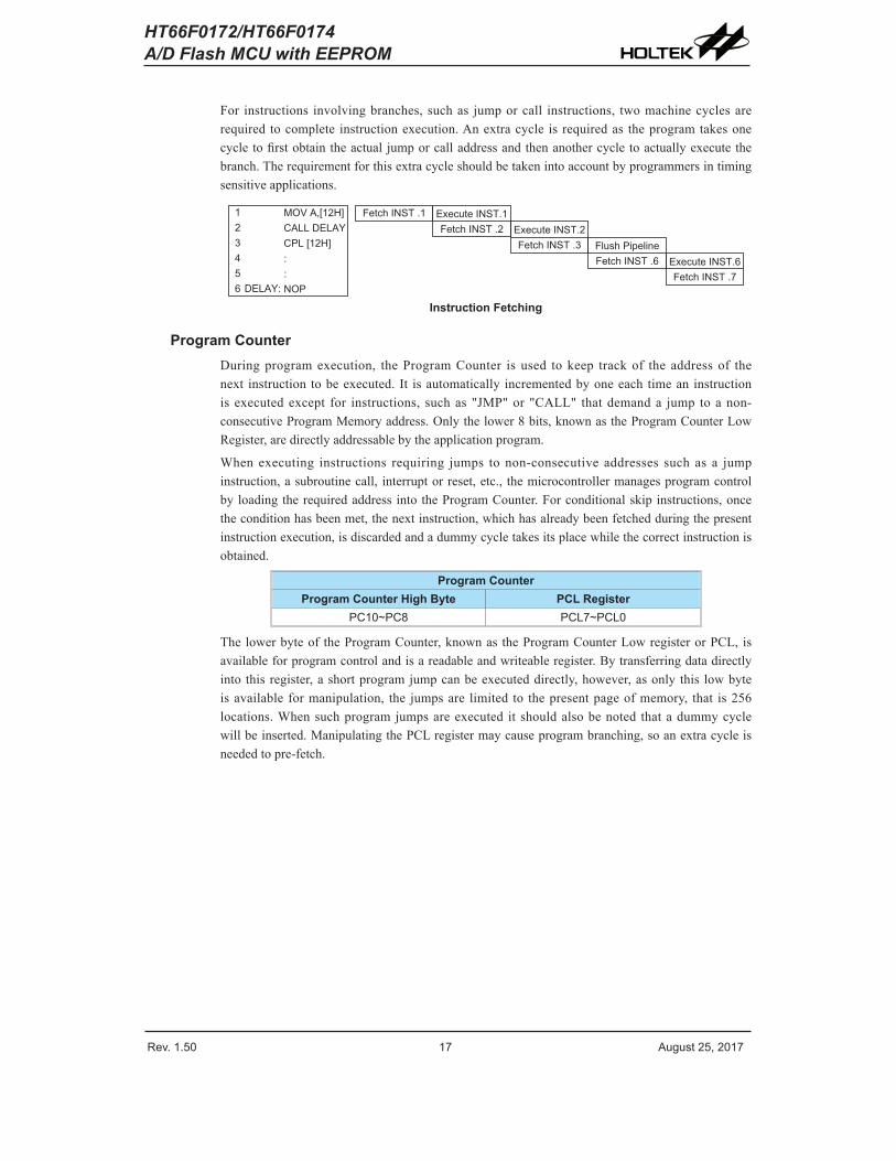
Clocking and PipeliningThemainsystemclock,derivedfromHXT,LXT,HIRCorLIRCoscillatorissubdividedintofourinternallygeneratednon-overlappingclocks,T1~T4.TheProgramCounter is incrementedat thebeginningoftheT1clockduringwhichtimeanewinstructionisfetched.TheremainingT2~T4clockscarryoutthedecodingandexecutionfunctions.Inthisway,oneT1~T4clockcycleformsoneinstructioncycle.Althoughthefetchingandexecutionofinstructionstakesplaceinconsecutiveinstructioncycles, thepipeliningstructureof themicrocontrollerensures that instructionsareeffectivelyexecuted inone instructioncycle.Theexception to thisare instructionswhere thecontentsoftheProgramCounterarechanged,suchassubroutinecallsorjumps,inwhichcasetheinstructionwilltakeonemoreinstructioncycletoexecute.
� � � � � � � � � � � � � � � �� � � � � � � � � � � � � � � � � � � � � � � � � � � � � � � � � � � �
� � � � � � � � � � � � � � � � � � � � � � � � � � � � � � � � � � � �� � � � � � � � � � � � � � � � � � �
� � � � � � � � �
� � � � � � � � � � � � � �
� � � � � � � � � � � � �
� � � � � � � � � � � � � � �
� � � � � � � � � � � � � �
� � � � � � � � � � � � � �
� � � � � � � � � � � � � �
� � � � � � � � � �
System Clock and Pipelining
Rev. 1.50 16 ����st �5� �01� Rev. 1.50 1� ����st �5� �01�
HT66F0172/HT66F0174A/D Flash MCU with EEPROM
For instructions involvingbranches,suchas jumporcall instructions, twomachinecyclesarerequired tocomplete instructionexecution.Anextracycle is requiredas theprogramtakesonecycletofirstobtaintheactualjumporcalladdressandthenanothercycletoactuallyexecutethebranch.Therequirementforthisextracycleshouldbetakenintoaccountbyprogrammersintimingsensitiveapplications.
� � � � � � � � � � � � � �� � � � � � � � � � � � �
� � � � � � � � � � � �� � � � � � � � � � � � �
� � � � � � � � � � � � � � � � � � � � � � � � � �
� � � � � � � � � � � � � �� � � � � � � � � � � �
� � � � � � � � � � � � ������
� � � � � � � � � �� � � � � � � � � � � � � � ���� � � � � �
Instruction Fetching
Program CounterDuringprogramexecution, theProgramCounter isused tokeep trackof theaddressof thenext instruction tobeexecuted. It isautomatically incrementedbyoneeach timean instructionisexecutedexcept for instructions, suchas"JMP"or"CALL" thatdemanda jump toanon-consecutiveProgramMemoryaddress.Onlythelower8bits,knownastheProgramCounterLowRegister,aredirectlyaddressablebytheapplicationprogram.
Whenexecuting instructions requiring jumps tonon-consecutiveaddresses suchas a jumpinstruction,asubroutinecall, interruptorreset,etc., themicrocontrollermanagesprogramcontrolbyloadingtherequiredaddressintotheProgramCounter.Forconditionalskipinstructions,oncetheconditionhasbeenmet,thenextinstruction,whichhasalreadybeenfetchedduringthepresentinstructionexecution,isdiscardedandadummycycletakesitsplacewhilethecorrectinstructionisobtained.
Program CounterProgram Counter High Byte PCL Register
PC10~PC8 PCL�~PCL0
Thelowerbyteof theProgramCounter,knownastheProgramCounterLowregisterorPCL,isavailableforprogramcontrolandisareadableandwriteableregister.Bytransferringdatadirectlyintothisregister,ashortprogramjumpcanbeexecuteddirectly,however,asonlythis lowbyteisavailableformanipulation, the jumpsare limited to thepresentpageofmemory, that is256locations.Whensuchprogramjumpsareexecuted itshouldalsobenoted thatadummycyclewillbeinserted.ManipulatingthePCLregistermaycauseprogrambranching,soanextracycleisneededtopre-fetch.

Rev. 1.50 18 ����st �5� �01� Rev. 1.50 19 ����st �5� �01�
HT66F0172/HT66F0174A/D Flash MCU with EEPROM
StackThis isaspecialpartof thememorywhichisusedtosavethecontentsof theProgramCounteronly.Thestackisneitherpartofthedatanorpartoftheprogramspace,andisneitherreadablenorwriteable.TheactivatedlevelisindexedbytheStackPointer,andisneitherreadablenorwriteable.Atasubroutinecallorinterruptacknowledgesignal,thecontentsoftheProgramCounterarepushedontothestack.Attheendofasubroutineoraninterruptroutine,signaledbyareturninstruction,RETorRETI,theProgramCounterisrestoredtoitspreviousvaluefromthestack.Afteradevicereset,theStackPointerwillpointtothetopofthestack.
Ifthestackisfullandanenabledinterrupttakesplace,theinterruptrequestflagwillberecordedbuttheacknowledgesignalwillbeinhibited.WhentheStackPointer isdecremented,byRETorRETI,theinterruptwillbeserviced.Thisfeaturepreventsstackoverflowallowingtheprogrammertousethestructuremoreeasily.However,whenthestackisfull,aCALLsubroutineinstructioncanstillbeexecutedwhichwillresult inastackoverflow.Precautionsshouldbetakentoavoidsuchcaseswhichmightcauseunpredictableprogrambranching.Ifthestackisoverflow,thefirstProgramCountersaveinthestackwillbelost.
� � � � � � � � � � � � � � �
� � � � � � � � � � � �
� � � � � � � � � � � � �
� � � � � � � � � � � � �
� � � � � � � � � � � �
� � � � � � � � � � � �
� � � � � � � � � � � �
� � � � �� � � � � � �
� � � � � � � � � � � � � � �
Arithmetic and Logic Unit – ALUThearithmetic-logicunitorALUisacriticalareaofthemicrocontrollerthatcarriesoutarithmeticandlogicoperationsoftheinstructionset.Connectedtothemainmicrocontrollerdatabus,theALUreceivesrelatedinstructioncodesandperformstherequiredarithmeticor logicaloperationsafterwhichtheresultwillbeplacedinthespecifiedregister.AstheseALUcalculationoroperationsmayresultincarry,borroworotherstatuschanges,thestatusregisterwillbecorrespondinglyupdatedtoreflectthesechanges.TheALUsupportsthefollowingfunctions:
• Arithmeticoperations:ADD,ADDM,ADC,ADCM,SUB,SUBM,SBC,SBCM,DAA
• Logicoperations:AND,OR,XOR,ANDM,ORM,XORM,CPL,CPLA
• RotationRRA,RR,RRCA,RRC,RLA,RL,RLCA,RLC
• IncrementandDecrementINCA,INC,DECA,DEC
• Branchdecision,JMP,SZ,SZA,SNZ,SIZ,SDZ,SIZA,SDZA,CALL,RET,RETI

Rev. 1.50 18 ����st �5� �01� Rev. 1.50 19 ����st �5� �01�
HT66F0172/HT66F0174A/D Flash MCU with EEPROM
Flash Program MemoryTheProgramMemoryisthelocationwheretheusercodeorprogramisstored.ForthisdevicetheProgramMemoryisFlashtype,whichmeansitcanbeprogrammedandre-programmeda largenumberof times,allowing theuser theconvenienceofcodemodificationon thesamedevice.Byusing theappropriateprogramming tools, thisFlashdeviceoffersusers the flexibility toconvenientlydebuganddeveloptheirapplicationswhilealsoofferingameansoffieldprogrammingandupdating.
StructureTheProgramMemoryhasacapacityof2K×16bits.TheProgramMemoryisaddressedby theProgramCounterandalsocontainsdata,tableinformationandinterruptsentries.Tabledata,whichcanbesetupinanylocationwithintheProgramMemory,isaddressedbyaseparatetablepointerregister.
000 H Reset
Interr�pt Vector
004 H
0�4 H
�FFH 16 bits
Program Memory Structure
Special VectorsWithintheProgramMemory,certainlocationsarereservedfortheresetandinterrupts.Thelocation000His reserved foruseby thedevice reset forprograminitialisation.Afteradevice reset isinitiated,theprogramwilljumptothislocationandbeginexecution.
Look-up TableAnylocationwithintheProgramMemorycanbedefinedasalook-uptablewhereprogrammerscanstorefixeddata.Tousethelook-uptable,thetablepointermustfirstbesetupbyplacingtheaddressof thelookupdatatoberetrievedinthetablepointerregister,TBLPandTBHP.Theseregistersdefinethetotaladdressofthelook-uptable.
Aftersettingupthetablepointer,thetabledatacanberetrievedfromtheProgramMemoryusingthe"TABRD[m]"or"TABRDL[m]"instructions,respectively.Whentheinstructionisexecuted,the lowerorder tablebyte from theProgramMemorywillbe transferred to theuserdefinedDataMemoryregister[m]asspecified in the instruction.Thehigherorder tabledatabytefromtheProgramMemorywillbe transferred to theTBLHspecial register.Anyunusedbits in thistransferredhigherorderbytewillbereadas"0".
Theaccompanyingdiagramillustratestheaddressingdataflowofthelook-uptable.
� � � � � � � � � � � � � � � � � � � � � � � � � �� � � � � � � �
� � � � � � � � � � � � � � �
� � � � � � � � � � � �
� � �
������� � � � � � � �
� � � � � � � � � � � � � �� � � � � � � � � � � �� � � � � � � � � � � �

Rev. 1.50 �0 ����st �5� �01� Rev. 1.50 �1 ����st �5� �01�
HT66F0172/HT66F0174A/D Flash MCU with EEPROM
InstructionTable Location Bits
b10 b9 b8 b7 b6 b5 b4 b3 b2 b1 b0T�BRD [m] @10 @9 @8 @� @6 @5 @4 @3 @� @1 @0T�BRDL [m] 1 1 1 @� @6 @5 @4 @3 @� @1 @0
Table LocationNote:b10~b0:Tablelocationbits
@7~@0:Tablepointer(TBLP)bits@10~@8:Tablepointer(TBHP)bits
Table Program ExampleThefollowingexampleshowshowthetablepointerandtabledataisdefinedandretrievedfromthemicrocontroller.ThisexampleusesrawtabledatalocatedintheProgramMemorywhichisstoredthereusingtheORGstatement.ThevalueatthisORGstatementis"700H"whichreferstothestartaddressofthelastpagewithinthe2KwordsProgramMemoryofthedevice.Thetablepointerissetupheretohaveaninitialvalueof"06H".ThiswillensurethatthefirstdatareadfromthedatatablewillbeattheProgramMemoryaddress"706H"or6locationsafterthestartofthelastpage.Notethatthevalueforthetablepointerisreferencedtothefirstaddressofthepresentpageifthe"TABRD[m]"instructionisbeingused.ThehighbyteofthetabledatawhichinthiscaseisequaltozerowillbetransferredtotheTBLHregisterautomaticallywhenthe"TABRD[m]"instructionisexecuted.Because theTBLHregister isaread-onlyregisterandcannotberestored,careshouldbe takentoensure itsprotection ifboth themain routineand InterruptServiceRoutineuse table readinstructions. Ifusing the tableread instructions, theInterruptServiceRoutinesmaychange thevalueoftheTBLHandsubsequentlycauseerrorsifusedagainbythemainroutine.Asaruleitisrecommendedthatsimultaneoususeofthetablereadinstructionsshouldbeavoided.However, insituationswheresimultaneoususecannotbeavoided,theinterruptsshouldbedisabledpriortotheexecutionofanymainroutinetable-readinstructions.Notethatalltablerelatedinstructionsrequiretwoinstructioncyclestocompletetheiroperation.
Table Read Program Exampletempreg1 db ? ; temporary register #1tempreg2 db ? ; temporary register #2::mov a,06h ; initialise low table pointer - note that this address is referencedmov tblp,a mov a,07h ; initialise high table pointermov tbhp,a::tabrd tempreg1 ; transfers value in table referenced by table pointer data at program ; memory address "706H" transferred to tempreg1 and TBLHdec tblp ; reduce value of table pointer by onetabrd tempreg2 ; transfers value in table referenced by table pointer data at program ; memory address "705H" transferred to tempreg2 and TBLH in this ; example the data "1AH" is transferred to tempreg1 and data "0FH" to ; register tempreg2::org 700h ; sets initial address of program memorydc 00Ah, 00Bh, 00Ch, 00Dh, 00Eh, 00Fh, 01Ah, 01Bh::

Rev. 1.50 �0 ����st �5� �01� Rev. 1.50 �1 ����st �5� �01�
HT66F0172/HT66F0174A/D Flash MCU with EEPROM
In Circuit ProgrammingTheprovisionofFlashtypeProgramMemoryprovidestheuserwithameansofconvenientandeasyupgradesandmodificationstotheirprogramsonthesamedevice.Asanadditionalconvenience,Holtekhasprovidedameansofprogrammingthemicrocontrollerin-circuitusinga4-pininterface.Thisprovidesmanufacturerswiththepossibilityofmanufacturingtheircircuitboardscompletewithaprogrammedorun-programmedmicrocontroller,andthenprogrammingorupgradingtheprogramata laterstage.Thisenablesproductmanufacturers toeasilykeep theirmanufacturedproductssuppliedwiththelatestprogramreleaseswithoutremovalandre-insertionofthedevice.
TheHoltekFlashMCUtoWriterProgrammingPincorrespondencetableisasfollows:
Holtek Write Pins MCU Programming Pins FunctionICPD� P�0 Pro�rammin� Serial Data/�ddressICPCK P�� Pro�rammin� Serial ClockVDD VDD Power S�pplyVSS VSS Gro�nd
During theprogrammingprocess, theusermust there takecare toensure thatnootheroutputsareconnectedtothesetwopins.TheProgramMemoryandEEPROMdatamemorycanbothbeprogrammedseriallyin-circuitusingthis4-wireinterface.Dataisdownloadedanduploadedseriallyonasinglepinwithanadditionallinefortheclock.Twoadditionallinesarerequiredforthepowersupply.The technicaldetails regardingthe in-circuitprogrammingof thedevicearebeyondthescopeofthisdocumentandwillbesuppliedinsupplementaryliterature.
� �
� � � � � � � � � �
� � � � �
� � � � �
� � � � � � � � � �
� � � � � � � � � � � � � � �
� �
� �
� � �
� � �
� � � � � � �� � � � � � � � � � � � � � � � �
� � �� � � � � � � � � � � � � � � �
Note:*mayberesistororcapacitor.Theresistanceof*mustbegreaterthan1korthecapacitanceof*mustbelessthan1nF.

Rev. 1.50 �� ����st �5� �01� Rev. 1.50 �3 ����st �5� �01�
HT66F0172/HT66F0174A/D Flash MCU with EEPROM
On-Chip Debug Support – OCDSAnEVchipexists for thepurposesofdeviceemulation.ThisEVchipdevicealsoprovidesan"On-ChipDebug" function todebug thedeviceduring thedevelopmentprocess.TheEVchipandtheactualMCUdevicearealmostfunctionallycompatibleexceptfor the"On-ChipDebug"function.UserscanusetheEVchipdevicetoemulatetherealchipdevicebehaviorbyconnectingtheOCDSDAandOCDSCKpinstotheHoltekHT-IDEdevelopmenttools.TheOCDSDApinistheOCDSData/Address input/outputpinwhile theOCDSCKpin is theOCDSclockinputpin.WhenusersusetheEVchipfordebugging,otherfunctionswhicharesharedwiththeOCDSDAandOCDSCKpinsintheactualMCUdevicewillhavenoeffectintheEVchip.However,thetwoOCDSpinswhicharepin-sharedwiththeICPprogrammingpinsarestillusedastheFlashMemoryprogrammingpins for ICP.ForamoredetailedOCDSdescription, refer to thecorrespondingdocumentnamed"Holteke-Linkfor8-bitMCUOCDSUser’sGuide".
Holtek e-Link Pins EV Chip Pins Pin DescriptionOCDSD� OCDSD� On-chip Deb�� S�pport Data/�ddress inp�t/o�tp�tOCDSCK OCDSCK On-chip Deb�� S�pport Clock inp�t
VDD VDD Power S�pplyGND VSS Gro�nd
RAM Data MemoryTheDataMemoryisavolatileareaof8-bitwideRAMinternalmemoryandisthelocationwheretemporaryinformationisstored.TheRAMDataMemorycapacityis128×8bits.
StructureDividedintotwosections,thefirstoftheseisanareaofRAM,knownastheSpecialFunctionDataMemory.Herearelocatedregisterswhicharenecessaryforcorrectoperationofthedevice.Manyoftheseregisterscanbereadfromandwrittentodirectlyunderprogramcontrol,however,someremainprotectedfromusermanipulation.ThesecondareaofDataMemoryisknownastheGeneralPurposeDataMemory,whichisreservedforgeneralpurposeuse.Alllocationswithinthisareaarereadandwriteaccessibleunderprogramcontrol.
Capacity Banks1�8 × 8 0: 80H~FFH

Rev. 1.50 �� ����st �5� �01� Rev. 1.50 �3 ����st �5� �01�
HT66F0172/HT66F0174A/D Flash MCU with EEPROM
00H I�R001H MP00�H I�R103H MP104H05H �CC06H PCL0�H TBLP08H TBLH09H TBHP0�H ST�TUS0BH SMOD0CH LVDC0DH INTEG0EH
WDTC
0FH
TBC
10H
INTC0
11H
INTC1
1�H
19H
PCPU
18HP�WU
1BH1�H
1DH1CH
1FH
P�P�C
1EH
�5H�6H
�9H�8H
�BH�CH�DH
35H
TM1C1
34H
TM1C0
36H
TM1DHTM1DL
TM1�HTM1�L
3�H
3�H
Read 0 only
3BH3CH
BP
13H14H
MFI0
15H
MFI1
16H1�H
�FH
TM0C1
�EH
TM0C0
30H
3�H
TM0DH
31H
TM0DL
TM0�H
33H
TM0�L
: Un�sed� read as 00H
INTC�
MFI�
Un�sedUn�sed
EE�EED
PCPUPB
PBC
��H
Un�sed
��H
TM0RPL
TM1RPL
3DH3EH
Un�sed
3FHEEC
Bank 0 Bank 1Bank 0 Bank 1
TMPC
CTRLLVRC
PC
38H39H
PCC
�DRH�DRL
�DCR0�DCR1�CERL
��H�3H�4H
�0H�1H
Un�sed
Un�sed
TM0RPH
TM1RPH
PBPU40H
�FH
HT66F0174
00H I�R001H MP00�H I�R103H MP104H05H �CC06H PCL0�H TBLP08H TBLH09H TBHP0�H ST�TUS0BH SMOD0CH LVDC0DH INTEG0EH
WDTC
0FH
TBC
10H
INTC0
11H
INTC1
1�H
19H
PCPU
18HP�WU
1BH1�H
1DH1CH
1FH
P�P�C
1EH
�5H�6H
�9H�8H
�BH�CH�DH
35H
TM1C1
34H
TM1C0
36H
TM1DHTM1DL
TM1�HTM1�L
3�H
3�H
Read 0 only
3BH3CH
BP
13H14H
MFI0
15H
MFI1
16H1�H
�FH
TM0C1
�EH
TM0C0
30H
3�H
TM0DH
31H
TM0DL
TM0�H
33H
TM0�L
: Un�sed� read as 00H
INTC�
MFI�
Un�sedUn�sed
PCPUPB
PBC
��H
Un�sed
��H
TM0RPL
TM1RPL
3DH3EH
Un�sed
3FH
Bank 0 Bank 1Bank 0 Bank 1
TMPC
CTRLLVRC
PC
38H39H
PCC
�DRH�DRL
�DCR0�DCR1�CERL
��H�3H�4H
�0H�1H
Un�sed
Un�sed
TM0RPH
TM1RPH
PBPU40H
�FH
Un�sedUn�sed
HT66F0172
Data Memory Structure
TheoverallDataMemoryissubdividedintotwobanks.TheSpecialPurposeDataMemoryregistersareaccessibleinallbanks,withtheexceptionoftheEECregisterataddress40H,whichisonlyaccessibleinBank1.SwitchingbetweenthedifferentDataMemorybanksisachievedbysettingtheBankPointertothecorrectvalue.ThestartaddressoftheDataMemoryforthedeviceistheaddress00H.
Rev. 1.50 �4 ����st �5� �01� Rev. 1.50 �5 ����st �5� �01�
HT66F0172/HT66F0174A/D Flash MCU with EEPROM
Special Function Register DescriptionMostoftheSpecialFunctionRegisterdetailswillbedescribedintherelevantfunctionalsections,howeverseveralregistersrequireaseparatedescriptioninthissection.
Indirect Addressing Registers – IAR0, IAR1TheIndirectAddressingRegisters,IAR0andIAR1,althoughhavingtheirlocationsinnormalRAMregisterspace,donotactuallyphysicallyexistasnormalregisters.ThemethodofindirectaddressingforRAMdatamanipulationuses theseIndirectAddressingRegistersandMemoryPointers, incontrasttodirectmemoryaddressing,wheretheactualmemoryaddressisspecified.ActionsontheIAR0andIAR1registerswillresultinnoactualreadorwriteoperationtotheseregistersbutrathertothememorylocationspecifiedbytheircorrespondingMemoryPointers,MP0orMP1.Actingasapair,IAR0andMP0cantogetheraccessdatafromBank0whiletheIAR1andMP1registerpaircanaccessdatafromanybank.AstheIndirectAddressingRegistersarenotphysicallyimplemented,readingtheIndirectAddressingRegistersindirectlywillreturnaresultof"00H"andwritingtotheregistersindirectlywillresultinnooperation.
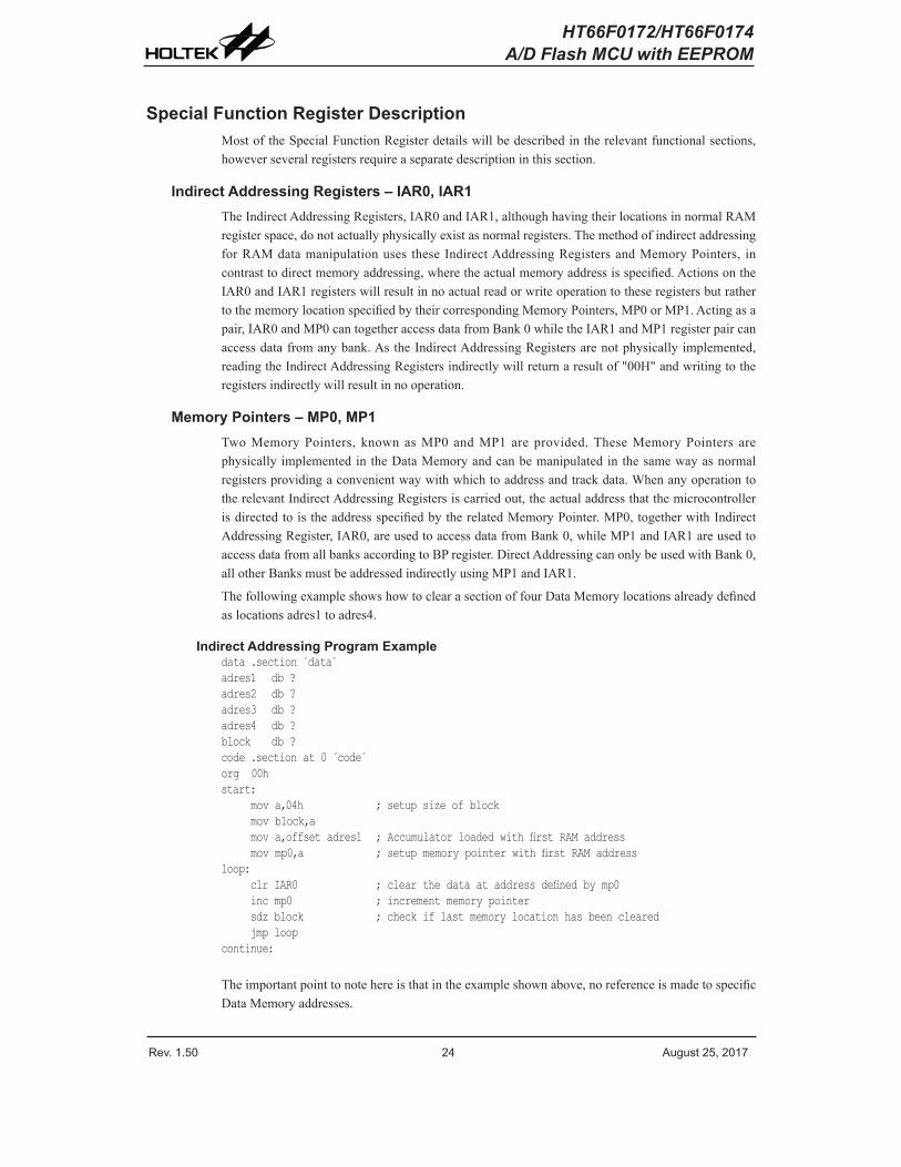
Memory Pointers – MP0, MP1TwoMemoryPointers, knownasMP0andMP1areprovided.TheseMemoryPointers arephysicallyimplementedintheDataMemoryandcanbemanipulatedinthesamewayasnormalregistersprovidingaconvenientwaywithwhichtoaddressandtrackdata.WhenanyoperationtotherelevantIndirectAddressingRegistersiscarriedout,theactualaddressthatthemicrocontrollerisdirectedtoistheaddressspecifiedbytherelatedMemoryPointer.MP0,togetherwithIndirectAddressingRegister,IAR0,areusedtoaccessdatafromBank0,whileMP1andIAR1areusedtoaccessdatafromallbanksaccordingtoBPregister.DirectAddressingcanonlybeusedwithBank0,allotherBanksmustbeaddressedindirectlyusingMP1andIAR1.
ThefollowingexampleshowshowtoclearasectionoffourDataMemorylocationsalreadydefinedaslocationsadres1toadres4.
Indirect Addressing Program Exampledata .section ´data´adres1 db ?adres2 db ?adres3 db ?adres4 db ?block db ? code .section at 0 code´org 00hstart: mov a,04h ; setup size of block mov block,a mov a,offset adres1 ; Accumulator loaded with first RAM address mov mp0,a ; setup memory pointer with first RAM addressloop: clr IAR0 ; clear the data at address defined by mp0 inc mp0 ; increment memory pointer sdz block ; check if last memory location has been cleared jmp loopcontinue:
Theimportantpointtonotehereisthatintheexampleshownabove,noreferenceismadetospecificDataMemoryaddresses.

Rev. 1.50 �4 ����st �5� �01� Rev. 1.50 �5 ����st �5� �01�
HT66F0172/HT66F0174A/D Flash MCU with EEPROM
Bank Pointer – BPFor thisdevice, theDataMemory isdivided into twobanks,Bank0andBank1.Selecting therequiredDataMemoryareaisachievedusingtheBankPointer.Bit0oftheBankPointerisusedtoselectDataMemoryBanks0~1.
TheDataMemoryisinitialisedtoBank0afterareset,exceptforaWDTtime-outresetinthePowerDownMode,inwhichcase,theDataMemorybankremainsunaffected.ItshouldbenotedthattheSpecialFunctionDataMemoryisnotaffectedbythebankselection,whichmeansthattheSpecialFunctionRegisterscanbeaccessedfromwithinanybank.DirectlyaddressingtheDataMemorywillalwaysresultinBank0beingaccessedirrespectiveofthevalueoftheBankPointer.AccessingdatafromBank1mustbeimplementedusingIndirectAddressing.
BP Register
Bit 7 6 5 4 3 2 1 0
Name — — — — — — — DMBP0
R/W — — — — — — — R/W
POR — — — — — — — 0
Bit7~1 Unimplemented,readas"0"Bit0 DMBP0:SelectDataMemoryBanks
0:Bank01:Bank1
Accumulator – ACCTheAccumulator iscentral to theoperationofanymicrocontrollerand isclosely relatedwithoperationscarriedoutby theALU.TheAccumulator is theplacewhereall intermediateresultsfromtheALUarestored.Without theAccumulator itwouldbenecessary towrite theresultofeachcalculationorlogicaloperationsuchasaddition,subtraction,shift,etc., totheDataMemoryresultinginhigherprogrammingandtimingoverheads.Data transferoperationsusually involvethetemporarystoragefunctionoftheAccumulator;forexample,whentransferringdatabetweenoneuser-definedregisterandanother, it isnecessary todo thisbypassing thedata throughtheAccumulatorasnodirecttransferbetweentworegistersispermitted.
Program Counter Low Register – PCLToprovideadditionalprogramcontrolfunctions, the lowbyteof theProgramCounter ismadeaccessibletoprogrammersbylocatingitwithintheSpecialPurposeareaoftheDataMemory.Bymanipulatingthisregister,directjumpstootherprogramlocationsareeasilyimplemented.LoadingavaluedirectlyintothisPCLregisterwillcauseajumptothespecifiedProgramMemorylocation,however,astheregisterisonly8-bitwide,onlyjumpswithinthecurrentProgramMemorypagearepermitted.Whensuchoperationsareused,notethatadummycyclewillbeinserted.
Look-up Table Registers – TBLP, TBHP, TBLHThesethreespecialfunctionregistersareusedtocontroloperationof thelook-uptablewhichisstoredintheProgramMemory.TBLPandTBHParethetablepointersandindicate thelocationwhere the tabledata is located.Theirvaluemustbesetupbeforeany tablereadcommandsareexecuted.Theirvaluecanbechanged,forexampleusingthe"INC"or"DEC"instructions,allowingforeasytabledatapointingandreading.TBLHisthelocationwherethehighorderbyteofthetabledataisstoredafteratablereaddatainstructionhasbeenexecuted.Notethatthelowerordertabledatabyteistransferredtoauserdefinedlocation.

Rev. 1.50 �6 ����st �5� �01� Rev. 1.50 �� ����st �5� �01�
HT66F0172/HT66F0174A/D Flash MCU with EEPROM
Status Register – STATUSThis8-bitregistercontainsthezeroflag(Z),carryflag(C),auxiliarycarryflag(AC),overflowflag(OV),powerdownflag(PDF),andwatchdogtime-outflag(TO).Thesearithmetic/logicaloperationandsystemmanagementflagsareusedtorecordthestatusandoperationofthemicrocontroller.
WiththeexceptionoftheTOandPDFflags,bitsinthestatusregistercanbealteredbyinstructionslikemostotherregisters.AnydatawrittenintothestatusregisterwillnotchangetheTOorPDFflag.Inaddition,operationsrelatedtothestatusregistermaygivedifferentresultsduetothedifferentinstructionoperations.TheTOflagcanbeaffectedonlybyasystempower-up,aWDTtime-outorbyexecutingthe"CLRWDT"or"HALT"instruction.ThePDFflagisaffectedonlybyexecutingthe"HALT"or"CLRWDT"instructionorduringasystempower-up.
TheZ,OV,ACandCflagsgenerallyreflectthestatusofthelatestoperations.
• Cissetifanoperationresultsinacarryduringanadditionoperationorifaborrowdoesnottakeplaceduringasubtractionoperation;otherwiseCiscleared.Cisalsoaffectedbyarotatethroughcarryinstruction.
• ACissetifanoperationresultsinacarryoutofthelownibblesinaddition,ornoborrowfromthehighnibbleintothelownibbleinsubtraction;otherwiseACiscleared.
• Zissetiftheresultofanarithmeticorlogicaloperationiszero;otherwiseZiscleared.
• OVissetifanoperationresultsinacarryintothehighest-orderbitbutnotacarryoutofthehighest-orderbit,orviceversa;otherwiseOViscleared.
• PDFisclearedbyasystempower-uporexecutingthe"CLRWDT"instruction.PDFissetbyexecutingthe"HALT"instruction.
• TOisclearedbyasystempower-uporexecutingthe"CLRWDT"or"HALT"instruction.TOissetbyaWDTtime-out.
Inaddition,onenteringaninterruptsequenceorexecutingasubroutinecall,thestatusregisterwillnotbepushedontothestackautomatically.Ifthecontentsofthestatusregistersareimportantandifthesubroutinecancorruptthestatusregister,precautionsmustbetakentocorrectlysaveit.
Rev. 1.50 �6 ����st �5� �01� Rev. 1.50 �� ����st �5� �01�
HT66F0172/HT66F0174A/D Flash MCU with EEPROM
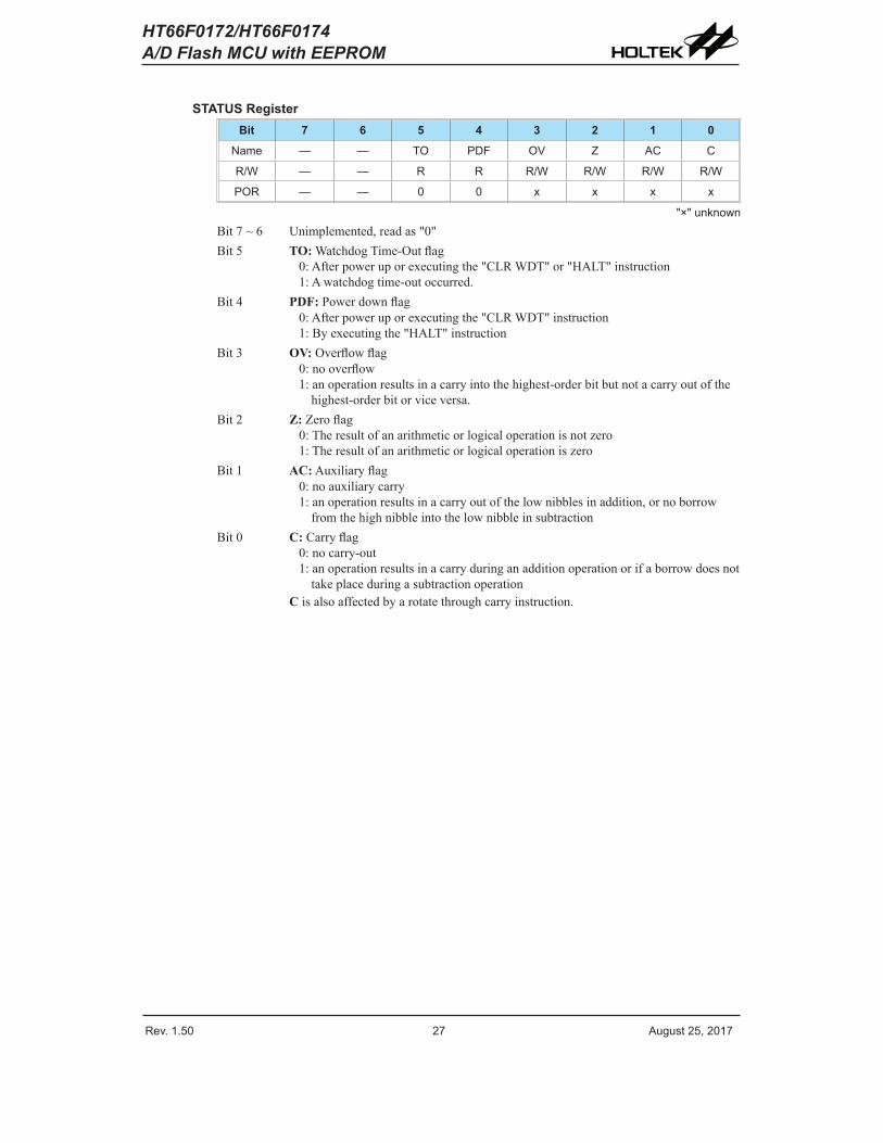
STATUS RegisterBit 7 6 5 4 3 2 1 0
Name — — TO PDF OV Z �C C
R/W — — R R R/W R/W R/W R/W
POR — — 0 0 x x x x
"×" �nknownBit7~6 Unimplemented,readas"0"Bit5 TO:WatchdogTime-Outflag
0:Afterpoweruporexecutingthe"CLRWDT"or"HALT"instruction1:Awatchdogtime-outoccurred.
Bit4 PDF:Powerdownflag0:Afterpoweruporexecutingthe"CLRWDT"instruction1:Byexecutingthe"HALT"instruction
Bit3 OV:Overflowflag0:nooverflow1:anoperationresultsinacarryintothehighest-orderbitbutnotacarryoutofthehighest-orderbitorviceversa.
Bit2 Z:Zeroflag0:Theresultofanarithmeticorlogicaloperationisnotzero1:Theresultofanarithmeticorlogicaloperationiszero
Bit1 AC:Auxiliaryflag0:noauxiliarycarry1:anoperationresultsinacarryoutofthelownibblesinaddition,ornoborrowfromthehighnibbleintothelownibbleinsubtraction
Bit0 C:Carryflag0:nocarry-out1:anoperationresultsinacarryduringanadditionoperationorifaborrowdoesnottakeplaceduringasubtractionoperation
Cisalsoaffectedbyarotatethroughcarryinstruction.

Rev. 1.50 �8 ����st �5� �01� Rev. 1.50 �9 ����st �5� �01�
HT66F0172/HT66F0174A/D Flash MCU with EEPROM
EEPROM Data Memory (only for HT66F0174)OneofthespecialfeaturesinthedeviceisitsinternalEEPROMDataMemory.EEPROM,whichstandsforElectricallyErasableProgrammableReadOnlyMemory,isbyitsnatureanon-volatileformofmemory,withdataretentionevenwhenitspowersupply is removed.Byincorporatingthiskindofdatamemory,awholenewhostofapplicationpossibilitiesaremadeavailabletothedesigner.TheavailabilityofEEPROMstorageallowsinformationsuchasproduct identificationnumbers,calibrationvalues,specificuserdata,systemsetupdataorotherproductinformationtobestoreddirectlywithintheproductmicrocontroller.TheprocessofreadingandwritingdatatotheEEPROMmemoryhasbeenreducedtoaverytrivialaffair.
EEPROM Data Memory StructureTheEEPROMDataMemorycapacityis64×8bits.UnliketheProgramMemoryandRAMDataMemory,theEEPROMDataMemoryisnotdirectlymappedintomemoryspaceandisthereforenotdirectlyaccessibleinthesamewayastheothertypesofmemory.InsteadithastobeaccessedindirectlythroughtheEEPROMcontrolregisters.
EEPROM RegistersThreeregisterscontroltheoveralloperationoftheinternalEEPROMDataMemory.Thesearetheaddressregister,EEA,thedataregister,EEDandasinglecontrolregister,EEC.AsboththeEEAandEEDregistersarelocatedinBank0,theycanbedirectlyaccessedinthesamewayasanyotherSpecialFunctionRegister.TheEECregisterhowever,beinglocatedinBank1,cannotbedirectlyaddresseddirectlyandcanonlybereadfromorwrittentoindirectlyusingtheMP1MemoryPointerandIndirectAddressingRegister,IAR1.BecausetheEECcontrolregisterislocatedataddress40HinBank1,theMP1MemoryPointermustfirstbesettothevalue40HandtheBankPointerregister,BP,settothevalue,01H,beforeanyoperationsontheEECregisterareexecuted.
EEPROM Control Registers List
NameBit
7 6 5 4 3 2 1 0
EE� — — D5 D4 D3 D� D1 D0
EED D� D6 D5 D4 D3 D� D1 D0
EEC — — — — WREN WR RDEN RD
EEA Register
Bit 7 6 5 4 3 2 1 0
Name — — D5 D4 D3 D� D1 D0
R/W — — R/W R/W R/W R/W R/W R/W
POR — — 0 0 0 0 0 0
Bit7~6 Unimplemented,readas"0"Bit5~0 D5~D0:DataEEPROMaddress
DataEEPROMaddressbit5~bit0

Rev. 1.50 �8 ����st �5� �01� Rev. 1.50 �9 ����st �5� �01�
HT66F0172/HT66F0174A/D Flash MCU with EEPROM
EED Register
Bit 7 6 5 4 3 2 1 0
Name D� D6 D5 D4 D3 D� D1 D0
R/W R/W R/W R/W R/W R/W R/W R/W R/W
POR 0 0 0 0 0 0 0 0
Bit7~0 D7~D0:DataEEPROMdataDataEEPROMdatabit7~bit0
EEC Register
Bit 7 6 5 4 3 2 1 0
Name — — — — WREN WR RDEN RD
R/W — — — — R/W R/W R/W R/W
POR — — — — 0 0 0 0
Bit7~4 Unimplemented,readas"0"Bit3 WREN:DataEEPROMWriteEnable
0:Disable1:Enable
This is theDataEEPROMWriteEnableBitwhichmustbesethighbeforeDataEEPROMwriteoperationsarecarriedout.Clearingthisbit tozerowill inhibitDataEEPROMwriteoperations.
Bit2 WR:EEPROMWriteControl0:Writecyclehasfinished1:Activateawritecycle
This is theDataEEPROMWriteControlBitandwhensethighbytheapplicationprogramwillactivateawritecycle.Thisbitwillbeautomaticallyresettozerobythehardwareafterthewritecyclehasfinished.SettingthisbithighwillhavenoeffectiftheWRENhasnotfirstbeensethigh.
Bit1 RDEN:DataEEPROMReadEnable0:Disable1:Enable
This is theDataEEPROMReadEnableBitwhichmustbesethighbeforeDataEEPROMreadoperationsarecarriedout.Clearingthisbit tozerowill inhibitDataEEPROMreadoperations.
Bit0 RD:EEPROMReadControl0:Readcyclehasfinished1:Activateareadcycle
This is theDataEEPROMReadControlBitandwhensethighbytheapplicationprogramwillactivateareadcycle.Thisbitwillbeautomaticallyresettozerobythehardwareafterthereadcyclehasfinished.SettingthisbithighwillhavenoeffectiftheRDENhasnotfirstbeensethigh.
Note:TheWREN,WR,RDENandRDcannotbesetto"1"atthesametimeinoneinstruction.TheWRandRDcannotbesetto"1"atthesametime.

Rev. 1.50 30 ����st �5� �01� Rev. 1.50 31 ����st �5� �01�
HT66F0172/HT66F0174A/D Flash MCU with EEPROM
Reading Data from the EEPROM ToreaddatafromtheEEPROM,thereadenablebit,RDEN,intheEECregistermustfirstbesethightoenablethereadfunction.TheEEPROMaddressofthedatatobereadmustthenbeplacedintheEEAregister.IftheRDbitintheEECregisterisnowsethigh,areadcyclewillbeinitiated.SettingtheRDbithighwillnotinitiateareadoperationif theRDENbithasnotbeenset.Whenthereadcycleterminates,theRDbitwillbeautomaticallyclearedtozero,afterwhichthedatacanbereadfromtheEEDregister.ThedatawillremainintheEEDregisteruntilanotherreadorwriteoperationisexecuted.Theapplicationprogramcanpoll theRDbit todeterminewhenthedataisvalidforreading.
Writing Data to the EEPROMTheEEPROMaddressofthedatatobewrittenmustfirstbeplacedintheEEAregisterandthedataplacedintheEEDregister.TowritedatatotheEEPROM,thewriteenablebit,WREN,intheEECregistermustfirstbesethightoenablethewritefunction.Afterthis,theWRbitintheEECregistermustbe immediatelysethighto initiateawritecycle.These twoinstructionsmustbeexecutedconsecutively.Theglobal interruptbitEMIshouldalsofirstbeclearedbefore implementinganywriteoperations,andthensetagainafterthewritecyclehasstarted.NotethatsettingtheWRbithighwillnotinitiateawritecycleiftheWRENbithasnotbeenset.AstheEEPROMwritecycleiscontrolledusinganinternaltimerwhoseoperationisasynchronoustomicrocontrollersystemclock,acertaintimewillelapsebeforethedatawillhavebeenwrittenintotheEEPROM.DetectingwhenthewritecyclehasfinishedcanbeimplementedeitherbypollingtheWRbitintheEECregisterorbyusingtheEEPROMinterrupt.Whenthewritecycleterminates,theWRbitwillbeautomaticallycleared tozeroby themicrocontroller, informing theuser that thedatahasbeenwritten to theEEPROM.TheapplicationprogramcanthereforepolltheWRbittodeterminewhenthewritecyclehasended.
Write ProtectionProtectionagainst inadvertentwriteoperation isprovided inseveralways.After thedevice ispowered-on theWriteEnablebit in thecontrol registerwillbeclearedpreventinganywriteoperations.Alsoatpower-ontheBankPointer,BP,willbereset tozero,whichmeansthatDataMemoryBank0willbeselected.AstheEEPROMcontrolregisterislocatedinBank1,thisaddsafurthermeasureofprotectionagainstspuriouswriteoperations.Duringnormalprogramoperation,ensuringthattheWriteEnablebitinthecontrolregisterisclearedwillsafeguardagainstincorrectwriteoperations.
EEPROM InterruptTheEEPROMwriteinterruptisgeneratedwhenanEEPROMwritecyclehasended.TheEEPROMinterruptmustfirstbeenabledbysettingtheDEEbitintherelevantinterruptregister.HoweverastheEEPROMiscontainedwithinaMulti-functionInterrupt,theassociatedmulti-functioninterruptenablebitmustalsobeset.WhenanEEPROMwritecycleends, theDEFrequest flagand itsassociatedmulti-functioninterruptrequestflagwillbothbeset.Iftheglobal,EEPROMandMulti-function interruptsareenabledandthestackisnotfull,a jumpto theassociatedMulti-functionInterruptvectorwilltakeplace.WhentheinterruptisservicedonlytheMulti-functioninterruptflagwillbeautomaticallyreset, theEEPROMinterruptflagmustbemanuallyresetbytheapplicationprogram.

Rev. 1.50 30 ����st �5� �01� Rev. 1.50 31 ����st �5� �01�
HT66F0172/HT66F0174A/D Flash MCU with EEPROM
Programming ConsiderationsCaremustbetakenthatdataisnotinadvertentlywrittentotheEEPROM.ProtectioncanbePeriodicbyensuringthattheWriteEnablebitisnormallyclearedtozerowhennotwriting.AlsotheBankPointercouldbenormallyclearedtozeroasthiswouldinhibitaccesstoBank1wheretheEEPROMcontrol register exist.Althoughcertainlynotnecessary, considerationmightbegiven in theapplicationprogramtothecheckingofthevalidityofnewwritedatabyasimplereadbackprocess.WhenwritingdatatheWRbitmustbesethighimmediatelyaftertheWRENbithasbeensethigh,toensurethewritecycleexecutescorrectly.Theglobal interruptbitEMIshouldalsobeclearedbeforeawritecycleisexecutedandthenre-enabledafterthewritecyclestarts.
Programming Examples• Reading data from the EEPROM - polling methodMOV A, EEPROM_ADRES ; user defined addressMOV EEA, AMOV A, 040H ; setup memory pointer MP1MOV MP1, A ; MP1 points to EEC registerMOV A, 01H ; setup Bank PointerMOV BP, ASET IAR1.1 ; set RDEN bit, enable read operationsSET IAR1.0 ; start Read Cycle - set RD bitBACK:SZ IAR1.0 ; check for read cycle endJMP BACKCLR IAR1 ; disable EEPROM writeCLR BPMOV A, EED ; move read data to registerMOV READ_DATA, A
• Writing Data to the EEPROM - polling methodMOV A, EEPROM_ADRES ; user defined addressMOV EEA, AMOV A, EEPROM_DATA ; user defined dataMOV EED, AMOV A, 040H ; setup memory pointer MP1MOV MP1, A ; MP1 points to EEC registerMOV A, 01H ; setup Bank PointerMOV BP, ACLR EMISET IAR1.3 ; set WREN bit, enable write operationsSET IAR1.2 ; start Write Cycle - set WR bitSET EMIBACK:SZ IAR1.2 ; check for write cycle endJMP BACKCLR IAR1 ; disable EEPROM writeCLR BP

Rev. 1.50 3� ����st �5� �01� Rev. 1.50 33 ����st �5� �01�
HT66F0172/HT66F0174A/D Flash MCU with EEPROM
OscillatorVariousoscillatoroptionsoffer theuserawide rangeof functionsaccording to theirvariousapplication requirements.The flexible featuresof theoscillator functionsensure that thebestoptimisationcanbeachievedintermsofspeedandpowersaving.Oscillatorselectionsandoperationareselectedthroughregisters.
Oscillator OverviewInadditiontobeingthesourceofthemainsystemclocktheoscillatorsalsoprovideclocksourcesfor theWatchdogTimerandTimeBaseInterrupts.Externaloscillators requiringsomeexternalcomponentsaswellas fully integrated internaloscillators, requiringnoexternalcomponents,areprovidedtoformawiderangeofbothfastandslowsystemoscillators.Alloscillatoroptionsareselected through theconfigurationoptions.Thehigher frequencyoscillatorsprovidehigherperformancebutcarrywithit thedisadvantageofhigherpowerrequirements,whiletheoppositeisofcoursetrueforthelowerfrequencyoscillators.Withthecapabilityofdynamicallyswitchingbetweenfastandslowsystemclock, thedevicehas theflexibility tooptimize theperformance/powerratio,afeatureespeciallyimportantinpowersensitiveportableapplications.
Type Name Freq. Pins
External Crystal HXT 400kHz~�0MHz OSC1/OSC�
Internal Hi�h Speed RC HIRC 8MHz —
External Low Speed Crystal LXT 3�.�68kHz XT1/XT�
Internal Low Speed RC LIRC 3�kHz —
Oscillator Types
System Clock ConfigurationsThereare fourmethodsofgenerating thesystemclock,highspeedoscillatorsand lowspeedoscillators.Thehighspeedoscillatorsaretheexternalcrystal/ceramicoscillatorandtheinternal8MHzRCoscillator.The lowspeedoscillator is the internal32kHz(LIRC)oscillatorand theexternal32.768kHzcrystaloscillator.Notethatthereisn'ttheexternal32.768kHzcrystaloscillatorinHT66F0172.SothelowspeedoscillatorfortheHT66F0172isonlytheinternal32kHz(LIRC)oscillator.Selectingwhether the loworhighspeedoscillator isusedas thesystemoscillator isimplementedusingtheHLCLKbitandCKS2~CKS0bitsintheSMODregisterandasthesystemclockcanbedynamicallyselected.
Theactual sourceclockused for thehigh speedand the lowspeedoscillators is chosenviaconfigurationoptions.The frequencyof the slowspeedorhigh speed systemclock is alsodeterminedusing theHLCLKbitandCKS2~CKS0bits in theSMODregister.Note that twooscillatorselectionsmustbemadenamelyonehighspeedandonelowspeedsystemoscillators.Itisnotpossibletochooseano-oscillatorselectionforeitherthehighorlowspeedoscillator.TheOSC1andOSC2pinsareusedtoconnecttheexternalcomponentsfortheexternalcrystal.

Rev. 1.50 3� ����st �5� �01� Rev. 1.50 33 ����st �5� �01�
HT66F0172/HT66F0174A/D Flash MCU with EEPROM
fH
fH /64
fH /3�
fH /16
fH/8
fH/4
fH/�
6- sta�e Prescaler
fSUB
Hi�h Speed Oscillation Confi��ration Option
fSYS
HLCLK� CKS�~CKS0 bits
Fast Wake �p from SLEEP Mode or IDLE Mode Control (for HXT only)
Hi�h SpeedOscillation
HXT
HIRC
Low SpeedOscillation
LXT
LIRC
fL
Low Speed Oscillation Confi��ration Option
Note:thereisnottheLXToscillatorinHT66F0172System Clock Configurations
External Crystal/Ceramic Oscillator – HXTTheExternalCrystal/CeramicSystemOscillator isoneof thehighfrequencyoscillatorchoices,whichisselectedviaconfigurationoption.Formostcrystaloscillatorconfigurations, thesimpleconnectionofacrystalacrossOSC1andOSC2willcreatethenecessaryphaseshiftandfeedbackforoscillation,withoutrequiringexternalcapacitors.However,forsomecrystaltypesandfrequencies,toensureoscillation,itmaybenecessarytoaddtwosmallvaluecapacitors,C1andC2.Usingaceramic resonatorwillusually require twosmallvaluecapacitors,C1andC2, tobeconnectedas shown foroscillation tooccur.ThevaluesofC1andC2shouldbe selected inconsultationwiththecrystalorresonatormanufacturer’sspecification..Foroscillatorstabilityandtominimisetheeffectsofnoiseandcrosstalk, it isimportanttoensurethatthecrystalandanyassociatedresistorsandcapacitorsalongwith interconnectinglinesarealllocatedasclosetotheMCUaspossible.
� � � �
� � � �
� �
� � � � � � � � � � �� � � � � � �
� � � � � � � �� � � � � � � � � �� � � � � � �
� �
� �
� �
� � � � � � � � � � � � � � � � � � � � � � � � � � � � � � � � � � � � � � � � � � � � � � � � � � � � � � � �� � � � � � � � � � � � � � � � � � � � � � � � � � � � � � � � � � � � � � � � � � � � � � � � � � � �� � � � � � � � � � � � � � � � � � � � � � � � � � � � �
Crystal/Resonator Oscillator – HXT
Crystal Osillator C1 and C2 ValuesCrystal Frequency C1 C2
1�MHz 0pF 0pF8MHz 0pF 0pF4MHz 0pF 0pF1MHz 100pF 100pF
Note: C1 and C� vales are for ��idance only.
Crystal Recommended Capacitor Values

Rev. 1.50 34 ����st �5� �01� Rev. 1.50 35 ����st �5� �01�
HT66F0172/HT66F0174A/D Flash MCU with EEPROM
Internal RC Oscillator – HIRCTheinternalRCoscillatorisafullyintegratedsystemoscillatorrequiringnoexternalcomponents.TheinternalRCoscillatorhasfixedfrequencyof8MHz.Devicetrimmingduringthemanufacturingprocessand the inclusionof internal frequencycompensationcircuitsareused toensure thatthe influenceof thepowersupplyvoltage, temperatureandprocessvariationsontheoscillationfrequencyareminimised.Asaresult,atapowersupplyofeither3Vor5Vandatatemperatureof25˚Cdegrees,thefixedoscillationfrequencyof8MHzwillhaveatolerancewithin2%.Notethatifthisinternalsystemclockoptionisselected,asitrequiresnoexternalpinsforitsoperation,I/OpinsPC0andPC1arefreeforuseasnormalI/Opins
External 32.768kHz Crystal Oscillator – LXTTheExternal32.768kHzCrystalSystemOscillatorisoneofthelowfrequencyoscillatorchoices,whichisselectedviaconfigurationoption.Thisclocksourcehasafixedfrequencyof32.768kHzandrequiresa32.768kHzcrystaltobeconnectedbetweenpinsXT1andXT2.Theexternalresistorandcapacitorcomponentsconnectedtothe32.768kHzcrystalarenecessarytoprovideoscillation.Forapplicationswhereprecise frequenciesareessential, thesecomponentsmayberequired toprovidefrequencycompensationduetodifferentcrystalmanufacturingtolerances.Duringpower-upthereisatimedelayassociatedwiththeLXToscillatorwaitingforittostart-up.
WhenthemicrocontrollerenterstheSLEEPorIDLEMode,thesystemclockisswitchedofftostopmicrocontrolleractivityand toconservepower.However, inmanymicrocontrollerapplicationsitmaybenecessary tokeep the internal timersoperationalevenwhenthemicrocontroller is intheSLEEPorIDLEMode.Todothis,anotherclock, independentof thesystemclock,mustbeprovided.
However,forsomecrystals,toensureoscillationandaccuratefrequencygeneration,itisnecessarytoaddtwosmallvalueexternalcapacitors,C1andC2.TheexactvaluesofC1andC2shouldbeselected inconsultationwith thecrystalor resonatormanufacturer’sspecification.Theexternalparallelfeedbackresistor,Rp,isrequired.
SomeconfigurationoptionsdetermineiftheXT1andXT2pinsareusedfortheLXToscillatororasI/Opins.
• If theLXToscillator isnotusedforanyclocksource, theXT1andXT2pinscanbeusedasnormalI/Opins.
• IftheLXToscillatorisusedforanyclocksource,the32.768kHzcrystalshouldbeconnectedtotheXT1andXT2pins.
Foroscillatorstabilityandtominimisetheeffectsofnoiseandcrosstalk, it isimportanttoensurethatthecrystalandanyassociatedresistorsandcapacitorsalongwith interconnectinglinesarealllocatedasclosetotheMCUaspossible.

Rev. 1.50 34 ����st �5� �01� Rev. 1.50 35 ����st �5� �01�
HT66F0172/HT66F0174A/D Flash MCU with EEPROM
� � � � � � � � � � �� � � � � � � �
� � � � � � � �� � � � � � � � � �� � � � � � �
� �
� �
� �
� � � � � � � � � � � � � � � � � � � � � � � � � � � � � � �� � � � � � � � � � � � � � � � � � � � � � � � � � � � � � � � �� � � � � � � � � � � � � � � � � � � � � � � � � � � � � � � � � � � � � � �
� � � � � � � � � � �� � � � � � � � � �� � � � � �
�
� � �
� � �
External LXT Oscillator
LXT Oscillator C1 and C2 ValuesCrystal Frequency C1 C2
3�.�68kHz 10pF 10pFNote: 1. C1 and C� val�es are for ��idance only. �. RP=5M~10M٠is recommended.
32.768kHz Crystal Recommended Capacitor Values
LXT Oscillator Low Power FunctionTheLXToscillatorcanfunctioninoneoftwomodes,theQuickStartModeandtheLowPowerMode.ThemodeselectionisexecutedusingtheLXTLPbitintheTBCregister.
LXTLP Bit LXT Mode0 Q�ick Start1 Low-power
Afterpoweron,theLXTLPbitwillbeautomaticallyclearedtozeroensuringthattheLXToscillatoris in theQuickStartoperatingmode.IntheQuickStartModetheLXToscillatorwillpowerupandstabilisequickly.However,after theLXToscillatorhas fullypoweredup itcanbeplacedintotheLow-powermodebysettingtheLXTLPbithigh.Theoscillatorwillcontinuetorunbutwithreducedcurrentconsumption,asthehighercurrentconsumptionisonlyrequiredduringtheLXToscillatorstart-up.Inpowersensitiveapplications,suchasbatteryapplications,wherepowerconsumptionmustbekepttoaminimum,itisthereforerecommendedthattheapplicationprogramsetstheLXTLPbithighabout2secondsafterpower-on.
Itshouldbenotedthat,nomatterwhatconditiontheLXTLPbit issetto, theLXToscillatorwillalwaysfunctionnormally,theonlydifferenceisthatitwilltakemoretimetostartupifintheLow-powermode.
Internal 32kHz Oscillator – LIRCTheInternal32kHzSystemOscillatorisalowfrequencyoscillatorchoice.It isafullyintegratedRCoscillatorwitha typicalfrequencyof32kHzat5V,requiringnoexternalcomponentsfor itsimplementation.Devicetrimmingduringthemanufacturingprocessandtheinclusionof internalfrequencycompensationcircuitsareusedtoensurethattheinfluenceofthepowersupplyvoltage,temperatureandprocessvariationson theoscillationfrequencyareminimised.Asaresult,atapowersupplyof5Vandatatemperatureof25˚Cdegrees,thefixedoscillationfrequencyof32kHzwillhaveatolerancewithin10%.
Supplementary ClocksThelowspeedoscillators,inadditiontoprovidingasystemclocksourcearealsousedtoprovideaclocksourcetootherdevicefunctions.ThesearetheWatchdogTimerandtheTimeBaseInterrupt.

Rev. 1.50 36 ����st �5� �01� Rev. 1.50 3� ����st �5� �01�
HT66F0172/HT66F0174A/D Flash MCU with EEPROM
Operating Modes and System ClocksPresentdayapplicationsrequirethat theirmicrocontrollershavehighperformancebutoftenstilldemandthattheyconsumeaslittlepoweraspossible,conflictingrequirementsthatareespeciallytrueinbatterypoweredportableapplications.Thefastclocksrequiredforhighperformancewillbytheirnatureincreasecurrentconsumptionandofcoursevice-versa, lowerspeedclocksreducecurrentconsumption.AsHoltekhasprovided thisdevicewithbothhighand lowspeedclocksourcesandthemeanstoswitchbetweenthemdynamically,theusercanoptimisetheoperationoftheirmicrocontrollertoachievethebestperformance/powerratio.
System ClocksThedevicehasmanydifferentclocksourcesforboththeCPUandperipheralfunctionoperation.Byprovidingtheuserwithawiderangeofclockoptionsusingconfigurationoptionsandregisterprogramming,aclocksystemcanbeconfiguredtoobtainmaximumapplicationperformance.Themainsystemclock,cancomefromeitherahighfrequency,fH,or lowfrequency,fL,source,and is selectedusing theHLCLKbit andCKS2~CKS0bits in theSMODregister.Thehighspeedsystemclockcanbesourcedfromeither theHXTor theHIRCoscillator,selectedviaaconfigurationoption.Thelowspeedsystemclocksourcecanbesourcedfromeither theLXTortheLIRCoscillator,selectedviaaconfigurationoption.ButforHT66F0172,thelowspeedsystemclocksourcecanonlybesourcedfromtheLIRCoscillator.Theotherchoice,whichisadividedversionofthehighspeedsystemoscillatorhasarangeoffH/2~fH/64.Therearetwoadditionalinternalclocksfor theperipheralcircuits, thesubstituteclock,fSUB,andtheTimeBaseclock, fTBC.Eachof these internalclocks issourcedbyeither theLXTorLIRCoscillators,selectedviaconfigurationoptions.ThefSUBclockisusedtoprovideasubstituteclockforthemicrocontrollerjustafterawake-uphasoccurredtoenablefasterwake-uptimes.
fH
fH /64
fH /3�
fH /16
fH/8
fH/4
fH/�
6- sta�e Prescaler
fSUB
Hi�h Speed Oscillation Confi��ration Option
fSYS
HLCLK� CKS�~CKS0 bits
Fast Wake- �p from SLEEP Mode or IDLE Mode Control (for HXT only)
TBCK
Time Base
WDT
fTBC
fTB
fSYS/4
fS
Hi�h SpeedOscillation
HXT
HIRC
Low SpeedOscillation
fL
LXT
LIRC
Confi��ration OptionLow Speed Oscillation
System Clock ConfigurationsNote:1.WhenthesystemclocksourcefSYSisswitchedtofLfromfH,thehighspeedoscillationwill
stoptoconservethepower.ThusthereisnofH~fH/64forperipheralcircuittouse.2.ThereisnottheLXToscillatorinHT66F0172

Rev. 1.50 36 ����st �5� �01� Rev. 1.50 3� ����st �5� �01�
HT66F0172/HT66F0174A/D Flash MCU with EEPROM
System Operation ModesThere are six differentmodesof operation for themicrocontroller, eachonewith its ownspecial characteristics andwhichcanbe chosenaccording to the specificperformanceandpowerrequirementsof theapplication.Thereare twomodesallowingnormaloperationof themicrocontroller, theNORMALModeandSLOWMode.Theremainingfourmodes,theSLEEP0,SLEEP1, IDLE0andIDLE1Modeareusedwhen themicrocontrollerCPUisswitchedoff toconservepower.
OperatingMode
DescriptionCPU fSYS fSUB fS fTBC
NORM�L Mode On fH~fH/64 On On OnSLOW Mode On fL On On OnIDLE0 Mode Off Off On On OnIDLE1 Mode Off On On On OnSLEEP0 Mode Off Off Off Off OffSLEEP1 Mode Off Off On On Off
NORMAL ModeAsthenamesuggeststhisisoneofthemainoperatingmodeswherethemicrocontrollerhasallofitsfunctionsoperationalandwherethesystemclockisprovidedbyoneofthehighspeedoscillator.Thismodeoperatesallowingthemicrocontrollertooperatenormallywithaclocksourcewillcomefromthehighspeedoscillator,either theHXTorHIRC.Thehighspeedoscillatorwillhoweverfirstbedividedbyaratiorangingfrom1to64,theactualratiobeingselectedbytheCKS2~CKS0andHLCLKbits in theSMODregister.Althoughahighspeedoscillator isused, running themicrocontrolleratadividedclockratioreducestheoperatingcurrent.
SLOW ModeThisisalsoamodewherethemicrocontrolleroperatesnormallyalthoughnowwithaslowerspeedclocksource.TheclocksourceusedwillbefromfL.Running themicrocontroller in thismodeallowsittorunwithmuchloweroperatingcurrents.IntheSLOWMode,thefHisoff.
SLEEP0 ModeTheSLEEPModeisenteredwhenanHALTinstructionisexecutedandwhentheIDLENbitintheSMODregisterislow.IntheSLEEP0modetheCPUwillbestopped.AndthefSUBandfSclockswillbestoppedtoo,andtheWatchdogTimerfunctionisdisabled.Inthismode,theLVDENismustsetto"0".IftheLVDENissetto"1",itwon’tentertheSLEEP0Mode.
SLEEP1 ModeTheSLEEPModeisenteredwhenanHALTinstruction isexecutedandwhentheIDLENbit intheSMODregisterislow.IntheSLEEP1modetheCPUwillbestopped.HoweverthefSUBandfSclockswillcontinuetooperateiftheLVDENis"1"ortheWatchdogTimerfunctionisenabled.
IDLE0 ModeTheIDLE0ModeisenteredwhenaHALTinstructionisexecutedandwhentheIDLENbitintheSMODregisterishighandtheFSYSONbitintheCTRLregisterislow.IntheIDLE0ModethesystemoscillatorwillbeinhibitedfromdrivingtheCPUbutsomeperipheralfunctionswillremainoperationalsuchastheWatchdogTimerandTMs.IntheIDLE0Mode,thesystemoscillatorwillbestopped.

Rev. 1.50 38 ����st �5� �01� Rev. 1.50 39 ����st �5� �01�
HT66F0172/HT66F0174A/D Flash MCU with EEPROM
IDLE1 ModeTheIDLE1ModeisenteredwhenanHALTinstructionisexecutedandwhentheIDLENbitintheSMODregisterishighandtheFSYSONbitintheCTRLregisterishigh.IntheIDLE1ModethesystemoscillatorwillbeinhibitedfromdrivingtheCPUbutmaycontinuetoprovideaclocksourcetokeepsomeperipheralfunctionsoperationalsuchastheWatchdogTimerandTMs.IntheIDLE1Mode,thesystemoscillatorwillcontinuetorun,andthissystemoscillatormaybehighspeedorlowspeedsystemoscillator.
Control RegisterAsingleregister,SMOD,isusedtooverallcontroloftheinternalclockswithinthedevice.
SMOD Register
Bit 7 6 5 4 3 2 1 0
Name CKS� CKS1 CKS0 FSTEN LTO HTO IDLEN HLCLK
R/W R/W R/W R/W R/W R R R/W R/W
POR 0 0 0 0 0 0 1 1
Bit7~5 CKS2 ~ CKS0:ThesystemclockselectionwhenHLCLKis"0"000:fL(fLXTorfLIRC)001:fL(fLXTorfLIRC)010:fH/64011:fH/32100:fH/16101:fH/8110:fH/4111:fH/2
Thesethreebitsareusedtoselectwhichclockisusedasthesystemclocksource.Inadditiontothesystemclocksource,whichcanbeeithertheLXTorLIRC,adividedversionofthehighspeedsystemoscillatorcanalsobechosenasthesystemclocksource.
Bit4 FSTEN:FastWake-upControl(onlyforHXT)0:Disable1:Enable
ThisistheFastWake-upControlbitwhichdeterminesifthefSUBclocksourceisinitiallyusedafterthedevicewakesup.Whenthebitishigh,thefSUBclocksourcecanbeusedasatemporarysystemclocktoprovideafasterwakeuptimeasthefSUBclockisavailable.
Bit3 LTO:Lowspeedsystemoscillatorreadyflag0:Notready1:Ready
ThisisthelowspeedsystemoscillatorSSTreadyflagwhichindicateswhenthelowspeedsystemoscillatorisstableafterpoweronresetorawake-uphasoccurred.TheflagwillbelowwhenintheSLEEP0Modebutafterawake-uphasoccurred,theflagwillchangetoahighlevelafter128clockcyclesiftheLXToscillatorisusedand1~2clockcyclesiftheLIRCoscillatorisused.
Bit2 HTO:Highspeedsystemoscillatorreadyflag0:Notready1:Ready
ThisisthehighspeedsystemoscillatorSSTreadyflagwhichindicateswhenthehighspeedsystemoscillatorisstableafterawake-uphasoccurred.Thisflagisclearedto"0"byhardwarewhenthedeviceispoweredonandthenchangestoahighlevelafterthehighspeedsystemoscillatorisstable.Thereforethisflagwillalwaysbereadas"1"bytheapplicationprogramafterdevicepower-on.TheflagwillbelowwhenintheSLEEPorIDLE0Modebutafterawake-uphasoccurred,theflagwillchangetoahighlevelafter128clockcyclesiftheHXToscillatorisusedandafter15~16clockcyclesiftheHIRCoscillatorisused.

Rev. 1.50 38 ����st �5� �01� Rev. 1.50 39 ����st �5� �01�
HT66F0172/HT66F0174A/D Flash MCU with EEPROM
Bit1 IDLEN:IDLEModeControl0:Disable1:Enable
This is theIDLEModeControlbitanddetermineswhathappenswhentheHALTinstructionisexecuted.If thisbit ishigh,whenaHALTinstructionisexecutedthedevicewillenter theIDLEMode. In theIDLE1Mode theCPUwillstoprunningbut thesystemclockwillcontinue tokeep theperipheral functionsoperational, ifFSYSONbitishigh.IfFSYSONbitislow,theCPUandthesystemclockwillallstopinIDLE0mode.IfthebitislowthedevicewillentertheSLEEPModewhenaHALTinstructionisexecuted.
Bit0 HLCLK:SystemClockSelection0:fH/2~fH/64orfL1:fH
Thisbit isusedtoselectif thefHclockorthefH/2~fH/64orfLclockisusedasthesystemclock.WhenthebitishighthefHclockwillbeselectedandiflowthefH/2~fH/64orfLclockwillbeselected.WhensystemclockswitchesfromthefHclocktothefLclockandthefHclockwillbeautomaticallyswitchedofftoconservepower.
CTRL Register
Bit 7 6 5 4 3 2 1 0
Name FSYSON — — — — LVRF LRF WRF
R/W R/W — — — — R/W R/W R/W
POR 0 — — — — x 0 0
Bit7 FSYSON:fSYSControlinIDLEMode0:Disable1:Enable
Bit6~3 Unimplemented,readas0.Bit2 LVRF:LVRfunctionresetflag
0:Notoccur1:Occurred
Thisbitissetto1whenaspecificLowVoltageResetsituationconditionoccurs.Thisbitcanonlybeclearedto0bytheapplicationprogram.
Bit1 LRF:LVRCControlregistersoftwareresetflag0:Notoccur1:Occurred
Thisbitissetto1iftheLVRCregistercontainsanynondefinedLVRvoltageregistervalues.Thisineffectactslikeasoftwareresetfunction.Thisbitcanonlybeclearedto0bytheapplicationprogram.
Bit0 WRF:WDTControlregistersoftwareresetflag0:Notoccur1:Occurred
Thisbit isset to1by theWDTControlregistersoftwareresetandclearedby theapplicationprogram.Note that thisbitcanonlybecleared to0by theapplicationprogram.

Rev. 1.50 40 ����st �5� �01� Rev. 1.50 41 ����st �5� �01�
HT66F0172/HT66F0174A/D Flash MCU with EEPROM
Fast Wake-upTominimisepowerconsumptionthedevicecanentertheSLEEPorIDLE0Mode,wherethesystemclocksourcetothedevicewillbestopped.Howeverwhenthedeviceiswokenupagain,itcantakeaconsiderabletimefortheoriginalsystemoscillatortorestart,stabilizeandallownormaloperationtoresume.ToensurethedeviceisupandrunningasfastaspossibleaFastWake-upfunctionisprovided,whichallowsfSUB,namelyeithertheLXTorLIRCoscillator,toactasatemporaryclocktofirstdrivethesystemuntil theoriginalsystemoscillatorhasstabilised.AstheclocksourcefortheFastWake-upfunctionisfSUB, theFastWake-upfunctionisonlyavailableintheSLEEP1andIDLE0modes.WhenthedeviceiswokenupfromtheSLEEP0mode,theFastWake-upfunctionhasnoeffectbecausethefSUBclockisstopped.TheFastWake-upenable/disablefunctioniscontrolledusingtheFSTENbitintheSMODregister.
If theHXToscillator isselectedas theNORMALModesystemclock,andif theFastWake-upfunctionisenabled,thenitwilltakeonetotwotSUBclockcyclesoftheLIRCorLXToscillatorforthesystemtowake-up.ThesystemwilltheninitiallyrununderthefSUBclocksourceuntil128HXTclockcycleshaveelapsed,atwhichpointtheHTOflagwillswitchhighandthesystemwillswitchovertooperatingfromtheHXToscillator.
If theHIRCoscillatorsorLIRCoscillatorisusedasthesystemoscillatorthenitwill take15~16clockcyclesofHIRCor1~2cyclesoftheLIRCtowakeupthesystemfromtheSLEEPorIDLE0Mode.TheFastWake-upbit,FSTENwillhavenoeffectinthesecases.
SystemOscillator
FSTENBit
Wake-up Time(SLEEP0 Mode)
Wake-up Time(SLEEP1 Mode)
Wake-up Time(IDLE0 Mode)
Wake-up Time(IDLE1 Mode)
HXT
0 1�8 HXT cycles 1�8 HXT cycles 1~� HXT cycles
1 1�8 HXT cycles1~� fSUB cycles(System r�ns with fSUB first for 51� HXT cycles and then switches over to r�n with the HXT clock)
1~� HXT cycles
HIRC X 15~16 HIRC cycles 15~16 HIRC cycles 1~� HIRC cycles
LIRC X 1~� LIRC cycles 1~� LIRC cycles 1~� LIRC cycles
LXT X 1�8 LTX cycles 1~� LXT cycles 1~� LXT cycles
Wake-Up Times
NotethatiftheWatchdogTimerisdisabled,whichmeansthattheLXTandLIRCarebothoff,thentherewillbenoFastWake-upfunctionavailablewhenthedevicewakes-upfromtheSLEEP0Mode.
Operating Mode Switching Thedevicecanswitchbetweenoperatingmodesdynamicallyallowingtheusertoselect thebestperformance/powerratiofor thepresent taskinhand.Inthiswaymicrocontrolleroperationsthatdonotrequirehighperformancecanbeexecutedusingslowerclocksthusrequiringlessoperatingcurrentandprolongingbatterylifeinportableapplications.
Insimpleterms,ModeSwitchingbetweentheNORMALModeandSLOWModeisexecutedusingtheHLCLKbitandCKS2~CKS0bitsintheSMODregisterwhileModeSwitchingfromtheNORMAL/SLOWModes to theSLEEP/IDLEModes isexecutedvia theHALTinstruction.WhenaHALTinstructionisexecuted,whetherthedeviceenterstheIDLEModeortheSLEEPModeisdeterminedbytheconditionoftheIDLENbitintheSMODregisterandFSYSONintheWDTCregister.

Rev. 1.50 40 ����st �5� �01� Rev. 1.50 41 ����st �5� �01�
HT66F0172/HT66F0174A/D Flash MCU with EEPROM
WhentheHLCLKbitswitchestoalowlevel,whichimpliesthatclocksourceisswitchedfromthehighspeedclocksource,fH,totheclocksource,fH/2~fH/64orfL.IftheclockisfromthefL,thehighspeedclocksourcewillstoprunningtoconservepower.WhenthishappensitmustbenotedthatthefH/16andfH/64internalclocksourceswillalsostoprunning,whichmayaffecttheoperationofotherinternalfunctionssuchas theTMs.Theaccompanyingflowchartshowswhathappenswhenthedevicemovesbetweenthevariousoperatingmodes.
� � � � � �� � � � � � � � � � � � � � � � � � � � � � � � � � � �
� � � � � � �� � � � � � � � � � � � �� � � � � � � �� � � � � � �
� � � � � � � � � � � � �
� � � � � �� � � � � � � � � � � �
� � � � �� � � � � �� � � � � �� � � � � � �� � � � � �
� � � � �� � � � � � � � � � � � � � � � � � � � � � � � � � � �
� � � � � � � � � � � �
� � � � � � � � � � �� � � � � � �� � � � � � �
� � � � �� � � � � � � � � � � � � � � � � � � � � � � � � � � �
� � � � � � � � � � � �
� � � � � �� � � � � � �� � � � � � �� � � � � �
� � � �� � � � � �� � � � �
� � � � � �� � � � � �� � � � � � �� � � � � �� � � � � �
� � � � � �� � � � � � � � � � � � � � � � � � � � � � � � � � � �
� � � � � � �� � � � � � � � � � � � �� � � � � � � �� � � � � �
� � � � � � � � � � � � �
NORMAL Mode to SLOW Mode SwitchingWhenrunningintheNORMALMode,whichusesthehighspeedsystemoscillator,andthereforeconsumesmorepower, thesystemclockcanswitch to run in theSLOWModebysetting theHLCLKbitto"0"andsettingtheCKS2~CKS0bitsto"000"or"001"intheSMODregister.Thiswillthenusethelowspeedsystemoscillatorwhichwillconsumelesspower.Usersmaydecidetodothisforcertainoperationswhichdonotrequirehighperformanceandcansubsequentlyreducepowerconsumption.
TheSLOWMode issourcedfromtheLIRCor theLXToscillatorand therefore requires theseoscillatorstobestablebeforefullmodeswitchingoccurs.ThisismonitoredusingtheLTObitintheSMODregister.
SLOW Mode to NORMAL Mode Switching InSLOWModethesystemuseseither theLXTorLIRClowspeedsystemoscillator.ToswitchbacktotheNORMALMode,wherethehighspeedsystemoscillatorisused,theHLCLKbitshouldbesetto"1"orHLCLKbitis"0",butCKS2~CKS0issetto"010","011","100","101","110"or"111".Asacertainamountof timewillberequiredfor thehighfrequencyclocktostabilise, thestatusof theHTObit ischecked.Theamountof timerequiredforhighspeedsystemoscillatorstabilizationdependsuponwhichhighspeedsystemoscillatortypeisused.

Rev. 1.50 4� ����st �5� �01� Rev. 1.50 43 ����st �5� �01�
HT66F0172/HT66F0174A/D Flash MCU with EEPROM
� � � � � � � � �
� � � � � � � � � � �
� � � � � � � � � � �
� � � � � � � � � �
� � � � � � � � � �
� � � � � � � � � � �
� � � � � � � � � � � � � � � �� � � � � � �
� � � � � � � � � � � � � � � � � � � � � � �� � � � � � � �� � � � � � � � � � � � � � � � � � � � � � � �
� � � � � � � � � � � � � � � �� � � � � � � �� � � � � � � � � � � � � � � � � � � � � � � �
� � � � � � � � � � � � � � � � �� � � � � � � � � � � � � � � � � � � � � � � �
� � � � � � � � � � � � � � � � �� � � � � � � � � � � � � � � � � � � � � � � �
� � � � � � � � � � �
� � � � � � � � � � �
� � � � � � � � � � �
� � � � � � � � � �
� � � � � � � � � �
� � � � � � � � �
� � � � � � � � � � � � � � � � � � � � � � � � �� � � � � � � � �
� � � � � � � � � � � � � � � � � � � � � � �� � � � � � � � �� � � � � � � � � � � � � � � � � � � � � � � � �
� � � � � � � � � � � � � � � �� � � � � � � � �� � � � � � � � � � � � � � � � � � � � � � � � �
� � � � � � � � � � � � � � � � � � �� � � � � � � � � � � � � � � � � � � � � � � � �
� � � � � � � � � � � � � � � � � � �� � � � � � � � � � � � � � � � � � � � � � � � �

Rev. 1.50 4� ����st �5� �01� Rev. 1.50 43 ����st �5� �01�
HT66F0172/HT66F0174A/D Flash MCU with EEPROM
Entering the SLEEP0 ModeThereisonlyonewayforthedevicetoentertheSLEEP0Modeandthatistoexecutethe"HALT"instructionintheapplicationprogramwiththeIDLENbitinSMODregisterequalto"0"andtheWDTandLVDbothoff.Whenthisinstructionisexecutedundertheconditionsdescribedabove,thefollowingwilloccur:
• Thesystemclock,WDTclockandTimeBaseclockwillbestoppedandtheapplicationprogramwillstopatthe"HALT"instruction.
• TheDataMemorycontentsandregisterswillmaintaintheirpresentcondition.
• TheWDTwillbeclearedandstopped.
• TheI/Oportswillmaintaintheirpresentconditions.
• Inthestatusregister,thePowerDownflag,PDF,willbesetandtheWatchdogtime-outflag,TO,willbecleared.
Entering the SLEEP1 ModeThereisonlyonewayforthedevicetoentertheSLEEP1Modeandthatistoexecutethe"HALT"instructionintheapplicationprogramwiththeIDLENbitinSMODregisterequalto"0"andtheWDTorLVDon.When this instruction isexecutedunder theconditionsdescribedabove, thefollowingwilloccur:
• ThesystemclockandTimeBaseclockwillbestoppedandtheapplicationprogramwillstopatthe"HALT"instruction,buttheWDTorLVDwillremainwiththeclocksourcecomingfromthefSUBclock.
• TheDataMemorycontentsandregisterswillmaintaintheirpresentcondition.
• TheWDTwillbeclearedandresumecountingiftheWDTisenabled.
• TheI/Oportswillmaintaintheirpresentconditions.
• Inthestatusregister,thePowerDownflag,PDF,willbesetandtheWatchdogtime-outflag,TO,willbecleared.
Entering the IDLE0 ModeThereisonlyonewayforthedevicetoentertheIDLE0Modeandthatistoexecutethe"HALT"instructionintheapplicationprogramwiththeIDLENbitinSMODregisterequalto"1"andtheFSYSONbitinCTRLregisterequalto"0".Whenthisinstructionisexecutedundertheconditionsdescribedabove,thefollowingwilloccur:
• Thesystemclockwillbestoppedandtheapplicationprogramwillstopatthe"HALT"instruc-tion,buttheTimeBaseclockfTBCandfSUBclockwillbeon.
• TheDataMemorycontentsandregisterswillmaintaintheirpresentcondition.
• TheWDTwillbeclearedandresumecountingiftheWDTisenabled.
• TheI/Oportswillmaintaintheirpresentconditions.
• Inthestatusregister,thePowerDownflag,PDF,willbesetandtheWatchdogtime-outflag,TO,willbecleared.

Rev. 1.50 44 ����st �5� �01� Rev. 1.50 45 ����st �5� �01�
HT66F0172/HT66F0174A/D Flash MCU with EEPROM
Entering the IDLE1 ModeThereisonlyonewayforthedevicetoentertheIDLE1Modeandthatistoexecutethe"HALT"instructionintheapplicationprogramwiththeIDLENbitinSMODregisterequalto"1"andtheFSYSONbitinCTRLregisterequalto"1".Whenthisinstructionisexecutedundertheconditionsdescribedabove,thefollowingwilloccur:
• ThesystemclockandTimeBaseclockandfSUBclockwillbeonandtheapplicationprogramwillstopatthe"HALT"instruction.
• TheDataMemorycontentsandregisterswillmaintaintheirpresentcondition.
• TheWDTwillbeclearedandresumecountingiftheWDTisenabled
• TheI/Oportswillmaintaintheirpresentconditions.
• Inthestatusregister,thePowerDownflag,PDF,willbesetandtheWatchdogtime-outflag,TO,willbecleared.
Standby Current ConsiderationsAsthemainreasonforenteringtheSLEEPorIDLEModeistokeepthecurrentconsumptionofthedevicetoaslowavalueaspossible,perhapsonlyintheorderofseveralmicro-ampsexceptintheIDLE1Mode,thereareotherconsiderationswhichmustalsobetakenintoaccountbythecircuitdesignerifthepowerconsumptionistobeminimised.SpecialattentionmustbemadetotheI/Opinsonthedevice.Allhigh-impedanceinputpinsmustbeconnectedtoeitherafixedhighorlowlevelasanyfloatinginputpinscouldcreateinternaloscillationsandresultinincreasedcurrentconsumption.Thisalsoappliestothedevicewhichhasdifferentpackagetypes,astheremaybeunbonbedpins.Thesemusteitherbesetupasoutputsorifsetupasinputsmusthavepull-highresistorsconnected.
Caremustalsobetakenwiththeloads,whichareconnectedtoI/Opins,whicharesetupasoutputs.Theseshouldbeplacedinaconditioninwhichminimumcurrent isdrawnorconnectedonlytoexternalcircuits thatdonotdrawcurrent,suchasotherCMOSinputs.Alsonote thatadditionalstandbycurrentwillalsoberequiredif theconfigurationoptionshaveenabledtheLXTorLIRCoscillator.
IntheIDLE1Modethesystemoscillatorison,ifthesystemoscillatorisfromthehighspeedsystemoscillator,theadditionalstandbycurrentwillalsobeperhapsintheorderofseveralhundredmicro-amps.

Rev. 1.50 44 ����st �5� �01� Rev. 1.50 45 ����st �5� �01�
HT66F0172/HT66F0174A/D Flash MCU with EEPROM
Wake-upAfterthesystementerstheSLEEPorIDLEMode,itcanbewokenupfromoneofvarioussourceslistedasfollows:
• AnexternalfallingedgeonPortA
• Asysteminterrupt
• AWDToverflow
If thesystemiswokenupbyanexternal reset, thedevicewillexperiencea full systemreset,however,ifthedeviceiswokenupbyaWDToverflow,aWatchdogTimerresetwillbeinitiated.Althoughbothof thesewake-upmethodswill initiatearesetoperation, theactualsourceof thewake-upcanbedeterminedbyexaminingtheTOandPDFflags.ThePDFflag isclearedbyasystempower-uporexecutingtheclearWatchdogTimerinstructionsandissetwhenexecutingthe"HALT"instruction.TheTOflagissetifaWDTtime-outoccurs,andcausesawake-upthatonlyresetstheProgramCounterandStackPointer,theotherflagsremainintheiroriginalstatus.
EachpinonPortAcanbesetupusingthePAWUregistertopermitanegativetransitiononthepintowake-upthesystem.WhenaPortApinwake-upoccurs,theprogramwillresumeexecutionattheinstructionfollowingthe"HALT"instruction.If thesystemiswokenupbyaninterrupt, thentwopossiblesituationsmayoccur.Thefirstiswheretherelatedinterruptisdisabledortheinterruptisenabledbutthestackisfull,inwhichcasetheprogramwillresumeexecutionattheinstructionfollowingthe"HALT"instruction.Inthissituation,theinterruptwhichwoke-upthedevicewillnotbeimmediatelyserviced,butwillratherbeservicedlaterwhentherelatedinterruptisfinallyenabledorwhenastacklevelbecomesfree.Theothersituationiswheretherelatedinterruptisenabledandthestackisnotfull,inwhichcasetheregularinterruptresponsetakesplace.Ifaninterruptrequestflag issethighbeforeentering theSLEEPorIDLEMode, thewake-upfunctionof therelatedinterruptwillbedisabled.
Programming ConsiderationsThehighspeedandlowspeedoscillatorsbothusethesameSSTcounter.Forexample,ifthesystemiswokenupfromtheSLEEP0ModeandboththeHIRCandLXToscillatorsneedtostart-upfromanoffstate.TheLXToscillatoruses theSSTcounterafterHIRCoscillatorhasfinisheditsSSTperiod.
• IfthedeviceiswokenupfromtheSLEEP0ModetotheNORMALMode,thehighspeedsystemoscillatorneedsanSSTperiod.ThedevicewillexecutefirstinstructionafterHTOis"1".Atthistime,theLXToscillatormaynotbestabilityiffSUBisfromLXToscillator.Thesamesituationoccursinthepower-onstate.TheLXToscillatorisnotreadyyetwhenthefirstinstructionisexecuted.
• IfthedeviceiswokenupfromtheSLEEP1ModetoNORMALMode,andthesystemclocksourceisfromHXToscillatorandFSTENis"1",thesystemclockcanbeswitchedtotheLIRCoscillatorafterwakeup.
• ThereareperipheralfunctionsforwhichthefSYSisused.IfthesystemclocksourceisswitchedfromfHtofL,theclocksourcetotheperipheralfunctionsmentionedabovewillchangeaccord-ingly.
• Theon/offconditionoffSdependsuponwhethertheWDTisenabledordisabledastheWDTclocksourceisselectedfromfS.

Rev. 1.50 46 ����st �5� �01� Rev. 1.50 4� ����st �5� �01�
HT66F0172/HT66F0174A/D Flash MCU with EEPROM
Watchdog TimerTheWatchdogTimerisprovidedtopreventprogrammalfunctionsorsequencesfromjumpingtounknownlocations,duetocertainuncontrollableexternaleventssuchaselectricalnoise.
Watchdog Timer Clock SourceTheWatchdogTimerclocksourceisprovidedbytheinternalfsclockwhichissourcedfromLXTorLIRCoscillatorchosenviaaconfigurationoption.TheWatchdogTimersourceclockis thensubdividedbyaratioof28to218togivelongertimeouts, theactualvaluebeingchosenusingtheWS2~WS0bits intheWDTCregister.TheLXToscillator issuppliedbyanexternal32.768kHzcrystal.TheLIRCinternaloscillatorhasanapproximateperiodof32kHzatasupplyvoltageof5V.However,itshouldbenotedthatthisspecifiedinternalclockperiodcanvarywithVDD,temperatureandprocessvariations.
NotethattheWatchdogTimerfunctioniscontrolledbyapplicationprogramandisallowedtoenableordisableWDTbyapplicationprogram.
Watchdog Timer Control RegisterAsingle register,WDTC,controls therequired timeoutperiodaswellas theenableordisableoperation.ThisregistercontrolstheoveralloperationoftheWatchdogTimer.
WDTC Register
Bit 7 6 5 4 3 2 1 0
Name WE4 WE3 WE� WE1 WE0 WS� WS1 WS0
R/W R/W R/W R/W R/W R/W R/W R/W R/W
POR 0 1 0 1 0 0 1 1
Bit7~3 WE4 ~ WE0:WDTfunctionsoftwarecontrol10101:Disabled01010:EnabledOther:ResetMCU
Whenthesebitsarechangedbytheenvironmentalnoisetoresetthemicrocontroller,theresetoperationwillbeactivatedafter2~3LIRCclockcyclesandtheWRFbitintheCTRLregisterwillbesetto1.
Bit2~0 WS2 ~ WS0:WDTTime-outperiodselection000:28/fS
001:210/fS
010:212/fS
011:214/fS
100:215/fS
101:216/fS
110:217/fS
111:218/fS
These threebitsdetermine thedivisionratioof theWatchdogTimersourceclock,whichinturndeterminesthetimeoutperiod.

Rev. 1.50 46 ����st �5� �01� Rev. 1.50 4� ����st �5� �01�
HT66F0172/HT66F0174A/D Flash MCU with EEPROM
CTRL Register
Bit 7 6 5 4 3 2 1 0
Name FSYSON — — — — LVRF LRF WRF
R/W R/W — — — — R/W R/W R/W
POR 0 — — — — × 0 0
Bit7 FSYSON:fSYSControlinIDLEModeDescribeelsewhere
Bit6~3 Unimplemented,readas"0"Bit2 LVRF:LVRfunctionresetflag
DescribeelsewhereBit1 LRF:LVRControlregistersoftwareresetflag
DescribeelsewhereBit0 WRF:WDTControlregistersoftwareresetflag
0:Notoccur1:Occurred
Thisbit isset to1by theWDTControlregistersoftwareresetandclearedby theapplicationprogram.Note that thisbitcanonlybecleared to0by theapplicationprogram.
Watchdog Timer OperationTheWatchdogTimeroperatesbyprovidingadeviceresetwhenits timeroverflows.ThismeansthatintheapplicationprogramandduringnormaloperationtheuserhastostrategicallycleartheWatchdogTimerbeforeitoverflowstopreventtheWatchdogTimerfromexecutingareset.Thisisdoneusingtheclearwatchdoginstructions.Iftheprogrammalfunctionsforwhateverreason,jumpstoanunknownlocation,orentersanendlessloop,theclearWDTinstructionwillnotbeexecutedinthecorrectmanner,inwhichcasetheWatchdogTimerwilloverflowandresetthedevice.WithregardtotheWatchdogTimerenable/disablefunction,therearefivebits,WE4~WE0,intheWDTCregister toofferadditionalenableordisableandresetcontrolof theWatchdogTimer.TheWDTfunctionwillbedisabledwhentheWE4~WE0bitsaresettoavalueof10101B.TheWDTfunctionwillbeenablediftheWE4~WE0bitsvalueisequalto01010B.IftheWE4~WE0bitsaresettoanyothervaluesbytheenvironmentalnoise,except01010Band10101B,itwillresetthedeviceafter2~3LIRCclockcycles.Afterpoweronthesebitswillhavethevalueof01010B.
WDT Function Control WE4 ~ WE0 Bits WDT Function
�pplication Pro�ram Enabled
10101B Disable
01010B Enable
�ny other val�e Reset MCU
Watchdog Timer Enable/Disable Control
Undernormalprogramoperation,aWatchdogTimertime-outwill initialiseadeviceresetandsetthestatusbitTO.However,ifthesystemisintheSLEEPorIDLEMode,whenaWatchdogTimertime-outoccurs,theTObitinthestatusregisterwillbesetandonlytheProgramCounterandStackPointerwillbereset.SeveralmethodscanbeadoptedtoclearthecontentsoftheWatchdogTimer.Thefirst isaWDTsoftwarereset,whichmeansacertainvalueiswrittenintotheWE4~WE0bitfieldexcept01010Band10101B,thesecondisusingtheWatchdogTimersoftwareclearinstructionandthethirdisviaaHALTinstruction.
ThereisonlyonemethodofusingsoftwareinstructiontocleartheWatchdogTimer.Thatistousethesingle"CLRWDT"instructiontocleartheWDT.

Rev. 1.50 48 ����st �5� �01� Rev. 1.50 49 ����st �5� �01�
HT66F0172/HT66F0174A/D Flash MCU with EEPROM
Themaximumtime-outperiodiswhenthe218divisionratioisselected.Asanexample,witha32kHzLIRCoscillatorasitssourceclock,thiswillgiveamaximumwatchdogperiodofaround8secondsforthe218divisionratio,andaminimumtimeoutof7.8msforthe28divisionration.
“CLR WDT”Instr�ction
8-sta�e Divider WDT Prescaler
WE4~WE0 bitsWDTC Re�ister Reset MCU
LXT fS fS/�8
8-to-1 MUX
CLR
WS�~WS0(fS/�8 ~ fS/�18)
WDT Time-o�t(�8/fS ~ �18/fS)
LIRC
MUX
Low Speed Oscillator Confi��ration option
“H�LT”Instr�ction
Watchdog Timer
Reset and InitialisationAresetfunctionisafundamentalpartofanymicrocontrollerensuringthat thedevicecanbesettosomepredeterminedcondition irrespectiveofoutsideparameters.Themost important resetconditionisafterpowerisfirstappliedtothemicrocontroller.Inthiscase, internalcircuitrywillensure that themicrocontroller,afterashortdelay,willbe inawelldefinedstateandready toexecutethefirstprograminstruction.Afterthispower-onreset,certainimportantinternalregisterswillbesettodefinedstatesbeforetheprogramcommences.OneoftheseregistersistheProgramCounter,whichwillberesettozeroforcingthemicrocontrollertobeginprogramexecutionfromthelowestProgramMemoryaddress.
Another typeofreset iswhentheWatchdogTimeroverflowsandresets themicrocontroller.Alltypesofresetoperationsresultindifferentregisterconditionsbeingsetup.AnotherresetexistsintheformofaLowVoltageReset,LVR,whereafullresetisimplementedinsituationswherethepowersupplyvoltagefallsbelowacertainthreshold.
Reset FunctionsTherearemore thanoneway inwhich themicrocontrollercanbereset,eachofwhichwillbedescribedasfollows.
Power-on ResetThemostfundamentalandunavoidablereset is theonethatoccursafterpowerisfirstappliedtothemicrocontroller.AswellasensuringthattheProgramMemorybeginsexecutionfromthefirstmemoryaddress,apower-onresetalsoensures thatcertainother registersarepreset toknownconditions.AlltheI/Oportandportcontrolregisterswillpowerupinahighconditionensuringthatallpinswillbefirstsettoinputs.
� � �
� � �
� � � � � � � � � � � � � �
� � � � � � �
� � � � � � � � � � �� � � � � � � � � � �
Power-On Reset Timing Chart

Rev. 1.50 48 ����st �5� �01� Rev. 1.50 49 ����st �5� �01�
HT66F0172/HT66F0174A/D Flash MCU with EEPROM
Low Voltage Reset – LVRThemicrocontrollercontainsalowvoltageresetcircuitinordertomonitorthesupplyvoltageofthedevice.TheLVRfunctionisalwaysenabledwithaspecificLVRvoltage,VLVR.Ifthesupplyvoltageofthedevicedropstowithinarangeof0.9V~VLVRsuchasmightoccurwhenchangingthebattery,theLVRwillautomaticallyresetthedeviceinternallyandtheLVRFbitintheCTRLregisterwillalsobesetto1.ForavalidLVRsignal,alowvoltage,i.e.,avoltageintherangebetween0.9V~VLVRmustexistforgreaterthanthevaluetLVRspecifiedintheLVD&LVRcharacteristics.Ifthelowvoltagestatedoesnotexceedthisvalue,theLVRwill ignorethelowsupplyvoltageandwillnotperformaresetfunction.
TheactualVLVRvaluecanbe selectedby theLVS7~LVS0bits in theLVRCregister. If theLVS7~LVS0bitsarechangedtosomecertainvaluesbytheenvironmentalnoiseorsoftwaresetting,theLVRwillresetthedeviceafter2~3LIRCclockcycles.Whenthishappens,theLRFbitintheCTRLregisterwillbesetto1.Afterpowerontheregisterwillhavethevalueof01010101B.NotethattheLVRfunctionwillbeautomaticallydisabledwhenthedeviceentersthepowerdownmode.
� � �
� � � � � � � � � � � � � �
� � � � � � � � � � � �
Low Voltage Reset Timing Chart
• LVRC Register
Bit 7 6 5 4 3 2 1 0
Name LVS� LVS6 LVS5 LVS4 LVS3 LVS� LVS1 LVS0
R/W R/W R/W R/W R/W R/W R/W R/W R/W
POR 0 1 0 1 0 1 0 1
Bit7~0 LVS7 ~ LVS0:LVRVoltageSelectcontrol01010101:2.1V00110011:2.55V10011001:3.15V10101010:3.8VAnyothervalue:generatesMCUreset– re�ister is reset to POR val�e
Whenanactuallowvoltageconditionoccurs,asspecifiedbyoneofthefourdefinedLVRvoltagevaluesabove,anMCUresetwillbegenerated.Theresetoperationwillbeactivatedafter2~3LIRCclockcycles.Inthissituationtheregistercontentswillremainthesameaftersucharesetoccurs.
Anyregistervalue,otherthanthefourdefinedLVRvaluesabove,willalsoresultinthegenerationofanMCUreset.Theresetoperationwillbeactivatedafter2~3LIRCclockcycles.HoweverinthissituationtheregistercontentswillberesettothePORvalue.

Rev. 1.50 50 ����st �5� �01� Rev. 1.50 51 ����st �5� �01�
HT66F0172/HT66F0174A/D Flash MCU with EEPROM
• CTRL Register
Bit 7 6 5 4 3 2 1 0
Name FSYSON — — — — LVRF LRF WRF
R/W R/W — — — — R/W R/W R/W
POR 0 — — — — × 0 0
Bit7 FSYSON:fSYSControlIDLEModeDescribeelsewhere
Bit6~3 Unimplemented,readas"0"Bit2 LVRF:LVRfunctionresetflag
0:Notoccur1:Occurred
Thisbitissetto1whenaspecificLowVoltageResetsituationconditionoccurs.Thisbitcanonlybeclearedto0bytheapplicationprogram.
Bit1 LRF:LVRControlregistersoftwareresetflag0:Notoccur1:Occurred
Thisbitissetto1iftheLVRCregistercontainsanynondefinedLVRvoltageregistervalues.Thisineffectactslikeasoftwareresetfunction.Thisbitcanonlybeclearedto0bytheapplicationprogram.
Bit0 WRF:WDTControlregistersoftwareresetflagDescribeelsewhere
Watchdog Time-out Reset during Normal Operation TheWatchdogtime-outResetduringnormaloperationisthesameasahardwareLVRresetexceptthattheWatchdogtime-outflagTOwillbesetto"1".
� � � � � � � � � � � �
� � � � � � � � � � � �
� � � � � � � � � � � � �
WDT Time-out Reset during Normal Operation Timing Chart
Watchdog Time-out Reset during SLEEP or IDLE ModeTheWatchdogtime-outResetduringSLEEPorIDLEModeisa littledifferentfromotherkindsofreset.MostoftheconditionsremainunchangedexceptthattheProgramCounterandtheStackPointerwillbeclearedto"0"andtheTOflagwillbesetto"1".RefertotheA.C.CharacteristicsfortSSTdetails.
� � � �
� � � � � � � � � � � �
� � � � � � � � � � � � �
WDT Time-out Reset during SLEEP or IDLE Timing Chart

Rev. 1.50 50 ����st �5� �01� Rev. 1.50 51 ����st �5� �01�
HT66F0172/HT66F0174A/D Flash MCU with EEPROM
Reset Initial ConditionsThedifferent typesofresetdescribedaffect theresetflagsindifferentways.Theseflags,knownasPDFandTOare located in thestatus registerandarecontrolledbyvariousmicrocontrolleroperations,suchas theSLEEPorIDLEModefunctionorWatchdogTimer.Thereset flagsareshowninthetable:
TO PDF RESET Conditions
0 0 Power-on reset
� � LVR reset d�rin� NORM�L or SLOW Mode operation
1 � WDT time-o�t reset d�rin� NORM�L or SLOW Mode operation
1 1 WDT time-o�t reset d�rin� IDLE or SLEEP Mode operation
Note:"u"standsforunchanged
Thefollowingtableindicatesthewayinwhichthevariouscomponentsofthemicrocontrollerareaffectedafterapower-onresetoccurs.
Item Condition After RESET
Pro�ram Co�nter Reset to zero
Interr�pts �ll interr�pts will be disabled
WDT Clear after reset� WDT be�ins co�ntin�
Timer Mod�les Timer Mod�les will be t�rned off
Inp�t/O�tp�t Ports I/O ports will be set�p as inp�ts
Stack Pointer Stack Pointer will point to the top of the stack
Thedifferentkindsofresetsallaffecttheinternalregistersofthemicrocontrollerindifferentways.Toensurereliablecontinuationofnormalprogramexecutionafteraresetoccurs,itisimportanttoknowwhatconditionthemicrocontrolleris inafteraparticularresetoccurs.Thefollowingtabledescribeshoweachtypeofresetaffectseachofthemicrocontrollerinternalregisters.
Register Power On Reset LVR Reset WDT Time-out
(Normal Operation)WDT Time-out(SLEEP/IDLE)
MP0 x x x x x x x x x x x x x x x x x x x x x x x x � � � � � � � �MP1 x x x x x x x x x x x x x x x x x x x x x x x x � � � � � � � �BP - - - - - - - 0 - - - - - - - 0 - - - - - - - 0 - - - - - - - ��CC x x x x x x x x � � � � � � � � � � � � � � � � � � � � � � � �PCL 0 0 0 0 0 0 0 0 0 0 0 0 0 0 0 0 0 0 0 0 0 0 0 0 0 0 0 0 0 0 0 0TBLP x x x x x x x x � � � � � � � � � � � � � � � � � � � � � � � �TBLH x x x x x x x x � � � � � � � � � � � � � � � � � � � � � � � �TBHP - - - - - x x x - - - - - � � � - - - - - � � � - - - - - � � �ST�TUS - - 0 0 x x x x - - � � x x x x - - 1 � � � � � - - 1 1 � � � �SMOD 0 0 0 0 0 0 11 0 0 0 0 0 0 11 0 0 0 0 0 0 11 � � � � � � � �LVDC - - 0 0 - 0 0 0 - - 0 0 - 0 0 0 - - 0 0 - 0 0 0 - - � � – � � �INTEG - - - - 0 0 0 0 - - - - 0 0 0 0 - - - - 0 0 0 0 - - - - � � � �INTC0 - 0 - 0 0 - 0 0 - 0 - 0 0 - 0 0 - 0 - 0 0 - 0 0 - � - � � - � �INTC1 0 0 0 0 0 0 0 0 0 0 0 0 0 0 0 0 0 0 0 0 0 0 0 0 � � � � � � � �INTC� - - 0 0 - - 0 0 - - 0 0 - - 0 0 - - 0 0 - - 0 0 - - � � - - � �MFI0 - - 0 0 - - 0 0 - - 0 0 - - 0 0 - - 0 0 - - 0 0 - - � � - - � �MFI1 - - 0 0 - - 0 0 - - 0 0 - - 0 0 - - 0 0 - - 0 0 - - � � - - � �MFI� - - 0 0 - - 0 0 - - 0 0 - - 0 0 - - 0 0 - - 0 0 - - � � - - � �

Rev. 1.50 5� ����st �5� �01� Rev. 1.50 53 ����st �5� �01�
HT66F0172/HT66F0174A/D Flash MCU with EEPROM
Register Power On Reset LVR Reset WDT Time-out
(Normal Operation)WDT Time-out(SLEEP/IDLE)
P� 1 1 1 1 1 1 1 1 1 1 1 1 1 1 1 1 1 1 1 1 1 1 1 1 � � � � � � � �P�C 1 1 1 1 1 1 1 1 1 1 1 1 1 1 1 1 1 1 1 1 1 1 1 1 � � � � � � � �P�PU 0 0 0 0 0 0 0 0 0 0 0 0 0 0 0 0 0 0 0 0 0 0 0 0 � � � � � � � �P�WU 0 0 0 0 0 0 0 0 0 0 0 0 0 0 0 0 0 0 0 0 0 0 0 0 � � � � � � � �TMPC 0 - - - - - 0 0 0 - - - - - 0 0 0 - - - - - 0 0 � - - - - - � �WDTC 0 1 0 1 0 0 11 0 1 0 1 0 0 11 0 1 0 1 0 0 11 � � � � � � � �TBC 0 0 11 0 111 0 0 11 0 111 0 0 11 0 111 0 0 11 0 111EE� - - 0 0 0 0 0 0 - - 0 0 0 0 0 0 - - 0 0 0 0 0 0 - - � � � � � �EED 0 0 0 0 0 0 0 0 0 0 0 0 0 0 0 0 0 0 0 0 0 0 0 0 � � � � � � � ��DRL(�DRFS=0) x x x x - - - - x x x x - - - - x x x x - - - - � � � � - - - -�DRL(�DRFS=1) x x x x x x x x x x x x x x x x x x x x x x x x � � � � � � � ��DRH(�DRFS=0) x x x x x x x x x x x x x x x x x x x x x x x x � � � � � � � ��DRH(�DRFS=1) - - - - x x x x - - - - x x x x - - - - x x x x - - - - � � � ��DCR0 0 11 0 - 0 0 0 0 11 0 - 0 0 0 0 11 0 - 0 0 0 � � � � - � � ��DCR1 0 0 - 0 - 0 0 0 0 0 - 0 - 0 0 0 0 0 - 0 - 0 0 0 � � - � - � � ��CERL 1 1 1 1 1 1 1 1 1 1 1 1 1 1 1 1 1 1 1 1 1 1 1 1 � � � � � � � �CTRL 0 - - - - x 0 0 0 - - - - 0 0 0 0 - - - - 0 0 0 � - - - - � � �LVRC 0 1 0 1 0 1 0 1 0 1 0 1 0 1 0 1 0 1 0 1 0 1 0 1 � � � � � � � �TM0C0 0 0 0 0 0 - - - 0 0 0 0 0 - - - 0 0 0 0 0 - - - � � � � � - - -TM0C1 0 0 0 0 0 0 0 0 0 0 0 0 0 0 0 0 0 0 0 0 0 0 0 0 � � � � � � � �TM0DL 0 0 0 0 0 0 0 0 0 0 0 0 0 0 0 0 0 0 0 0 0 0 0 0 � � � � � � � �TM0DH 0 0 0 0 0 0 0 0 0 0 0 0 0 0 0 0 0 0 0 0 0 0 0 0 � � � � � � � �TM0�L 0 0 0 0 0 0 0 0 0 0 0 0 0 0 0 0 0 0 0 0 0 0 0 0 � � � � � � � �TM0�H 0 0 0 0 0 0 0 0 0 0 0 0 0 0 0 0 0 0 0 0 0 0 0 0 � � � � � � � �TM0RPL 0 0 0 0 0 0 0 0 0 0 0 0 0 0 0 0 0 0 0 0 0 0 0 0 � � � � � � � �TM0RPH 0 0 0 0 0 0 0 0 0 0 0 0 0 0 0 0 0 0 0 0 0 0 0 0 � � � � � � � �TM1C0 0 0 0 0 0 - - - 0 0 0 0 0 - - - 0 0 0 0 0 - - - � � � � � - - -TM1C1 0 0 0 0 0 0 0 0 0 0 0 0 0 0 0 0 0 0 0 0 0 0 0 0 � � � � � � � �TM1DL 0 0 0 0 0 0 0 0 0 0 0 0 0 0 0 0 0 0 0 0 0 0 0 0 � � � � � � � �TM1DH - - - - - - 0 0 - - - - - - 0 0 - - - - - - 0 0 - - - - - - � �TM1�L 0 0 0 0 0 0 0 0 0 0 0 0 0 0 0 0 0 0 0 0 0 0 0 0 � � � � � � � �TM1�H - - - - - - 0 0 - - - - - - 0 0 - - - - - - 0 0 - - - - - - � �TM1RPL 0 0 0 0 0 0 0 0 0 0 0 0 0 0 0 0 0 0 0 0 0 0 0 0 � � � � � � � �TM1RPH - - - - - - 0 0 - - - - - - 0 0 - - - - - - 0 0 - - - - - - � �PC - - - - - 1 1 1 - - - - - 1 1 1 - - - - - 1 1 1 - - - - - � � �PCC - - - - - 1 1 1 - - - - - 1 1 1 - - - - - 1 1 1 - - - - - � � �PCPU - - - - - 0 0 0 - - - - - 0 0 0 - - - - - 0 0 0 - - - - - � � �PB - 1 1 1 1 1 1 1 - 1 1 1 1 1 1 1 - 1 1 1 1 1 1 1 - � � � � � � �PBC - 1 1 1 1 1 1 1 - 1 1 1 1 1 1 1 - 1 1 1 1 1 1 1 - � � � � � � �PBPU - 0 0 0 0 0 0 0 - 0 0 0 0 0 0 0 - 0 0 0 0 0 0 0 - � � � � � � �EEC - - - - 0 0 0 0 - - - - 0 0 0 0 - - - - 0 0 0 0 - - - - � � � �
Note:"-"standsfor"unimplemented""u"standsfor"unchanged""x"standsfor"unknown"

Rev. 1.50 5� ����st �5� �01� Rev. 1.50 53 ����st �5� �01�
HT66F0172/HT66F0174A/D Flash MCU with EEPROM
Input/Output PortsHoltekmicrocontrollersofferconsiderableflexibilityontheirI/Oports.Withtheinputoroutputdesignationofeverypinfullyunderuserprogramcontrol,pull-highselectionsforallportsandwake-upselectionsoncertainpins,theuserisprovidedwithanI/Ostructuretomeettheneedsofawiderangeofapplicationpossibilities.
Thedeviceprovidesbidirectionalinput/outputlineslabeledwithportnamesPA,PBandPC.TheseI/OportsaremappedtotheRAMDataMemorywithspecificaddressesasshownintheSpecialPurposeDataMemorytable.AlloftheseI/Oportscanbeusedforinputandoutputoperations.Forinputoperation,theseportsarenon-latching,whichmeanstheinputsmustbereadyattheT2risingedgeofinstruction"MOVA,[m]",wheremdenotestheportaddress.Foroutputoperation,allthedataislatchedandremainsunchangeduntiltheoutputlatchisrewritten.
RegisterName
Bit
7 6 5 4 3 2 1 0
P� D� D6 D5 D4 D3 D� D1 D0
P�C D� D6 D5 D4 D3 D� D1 D0
P�PU D� D6 D5 D4 D3 D� D1 D0
P�WU D� D6 D5 D4 D3 D� D1 D0
PB — D6 D5 D4 D3 D� D1 D0
PBC — D6 D5 D4 D3 D� D1 D0
PBPU — D6 D5 D4 D3 D� D1 D0
PC — — — — — D� D1 D0
PCC — — — — — D� D1 D0
PCPU — — — — — D� D1 D0
I/O Register List
Pull-high ResistorsManyproductapplicationsrequirepull-highresistorsfortheirswitchinputsusuallyrequiringtheuseofanexternal resistor.Toeliminate theneedfor theseexternal resistors,all I/Opins,whenconfiguredasaninputhavethecapabilityofbeingconnectedtoaninternalpull-highresistor.Thesepull-highresistorsareselectedusingregistersPAPU~PCPU,andare implementedusingweakPMOStransistors.
PAPU Register
Bit 7 6 5 4 3 2 1 0Name D� D6 D5 D4 D3 D� D1 D0R/W R/W R/W R/W R/W R/W R/W R/W R/WPOR 0 0 0 0 0 0 0 0
Bit7~0 I/OPortAbit7~bit0Pull-HighControl0:Disable1:Enable

Rev. 1.50 54 ����st �5� �01� Rev. 1.50 55 ����st �5� �01�
HT66F0172/HT66F0174A/D Flash MCU with EEPROM
PBPU Register
Bit 7 6 5 4 3 2 1 0Name — D6 D5 D4 D3 D� D1 D0R/W — R/W R/W R/W R/W R/W R/W R/WPOR — 0 0 0 0 0 0 0
Bit7 Unimplemented,readas"0"Bit6~0 I/OPortBbit6~bit0Pull-HighControl
0:Disable1:Enable
PCPU Register
Bit 7 6 5 4 3 2 1 0Name — — — — — D� D1 D0R/W — — — — — R/W R/W R/WPOR — — — — — 0 0 0
Bit7~3 Unimplemented,readas"0"Bit2~0 I/OPortCbit2~bit0Pull-HighControl
0:Disable1:Enable
Port A Wake-upTheHALTinstructionforcesthemicrocontrollerintotheSLEEPorIDLEModewhichpreservespower,afeature that is importantforbatteryandother low-powerapplications.Variousmethodsexisttowake-upthemicrocontroller,oneofwhichistochangethelogicconditionononeofthePortApinsfromhightolow.Thisfunctionisespeciallysuitableforapplicationsthatcanbewokenupviaexternalswitches.EachpinonPortAcanbeselectedindividuallytohavethiswake-upfeatureusingthePAWUregister.
PAWU Register
Bit 7 6 5 4 3 2 1 0Name D� D6 D5 D4 D3 D� D1 D0R/W R/W R/W R/W R/W R/W R/W R/W R/WPOR 0 0 0 0 0 0 0 0
Bit7~0 I/OPortAbit7~bit0WakeUpControl0:Disable1:Enable

Rev. 1.50 54 ����st �5� �01� Rev. 1.50 55 ����st �5� �01�
HT66F0172/HT66F0174A/D Flash MCU with EEPROM
I/O Port Control RegistersEach I/Oporthas itsowncontrol registerknownasPAC~PCC, to control the input/outputconfiguration.With this control register, eachCMOSoutput or input canbe reconfigureddynamicallyundersoftwarecontrol.Eachpinof theI/Oports isdirectlymappedtoabit in itsassociatedportcontrolregister.FortheI/Opintofunctionasaninput,thecorrespondingbitofthecontrolregistermustbewrittenasa"1".Thiswillthenallowthelogicstateoftheinputpintobedirectlyreadbyinstructions.Whenthecorrespondingbitofthecontrolregisteriswrittenasa"0",theI/OpinwillbesetupasaCMOSoutput.Ifthepiniscurrentlysetupasanoutput,instructionscanstillbeusedtoreadtheoutputregister.
However,itshouldbenotedthattheprogramwillinfactonlyreadthestatusoftheoutputdatalatchandnottheactuallogicstatusoftheoutputpin.
PAC Register
Bit 7 6 5 4 3 2 1 0Name D� D6 D5 D4 D3 D� D1 D0R/W R/W R/W R/W R/W R/W R/W R/W R/WPOR 1 1 1 1 1 1 1 1
Bit7~0 I/OPortAbit7~bit0Input/OutputControl0:Output1:Input
PBC Register
Bit 7 6 5 4 3 2 1 0Name — D6 D5 D4 D3 D� D1 D0R/W — R/W R/W R/W R/W R/W R/W R/WPOR — 1 1 1 1 1 1 1
Bit7 Unimplemented,readas"0"Bit6~0 I/OPortBbit6~bit0Input/OutputControl
0:Output1:Input
PCC Register
Bit 7 6 5 4 3 2 1 0
Name — — — — — D� D1 D0
R/W — — — — — R/W R/W R/W
POR — — — — — 1 1 1
Bit7~3 Unimplemented,readas"0"Bit2~0 I/OPortCbit2~bit0Input/OutputControl
0:Output1:Input

Rev. 1.50 56 ����st �5� �01� Rev. 1.50 5� ����st �5� �01�
HT66F0172/HT66F0174A/D Flash MCU with EEPROM
I/O Pin StructuresTheaccompanyingdiagrams illustrate the internalstructuresofsomegeneric I/Opin types.AstheexactlogicalconstructionoftheI/Opinwilldifferfromthesedrawings,theyaresuppliedasaguideonlytoassistwiththefunctionalunderstandingoftheI/Opins.Thewiderangeofpin-sharedstructuresdoesnotpermitalltypestobeshown.
� � �
���� � � � � � � � � � � � � � � � � �
� � � � � � � � � �� � � � �� � � � � �
� � � � � � �
� � � � � � � � � � � � � � � � � � � � �
� � � � � � � � � �
� � � � � � � � � � � � � � � � � � � �
� � � � � � � � � � � � � � � � � � �
� � � � � � � �
� � � �� �� �
� ��
�
� �
� ��
�
� � � � � � � � �
� � � � � � � � � � � �� � � � � � � � � � � � � � � � � �
Generic Input/Output Structure
� � �
���� � � � � � � � � � � � � � � � � �
� � � � � � � � � �� � � � �� � � � � �
� � � � � � �
� � � � � � � � � � � � � � � � � � � � �
� � � � � � � � � �
� � � � � � � � � � � � � � � � � � � �
� � � � � � � � � � � � � � � � � � �
� � � � � � � �
� � � � � � � � � � � � � �
� � � � � � � � �
� � � � � � � � � � � � � � � �
� � � �� �
� � � � � � � �
� � � � � �
� �
� ��
�
� �
� ��
�
A/D Input/Output Structure

Rev. 1.50 56 ����st �5� �01� Rev. 1.50 5� ����st �5� �01�
HT66F0172/HT66F0174A/D Flash MCU with EEPROM
Programming ConsiderationsWithintheuserprogram,oneofthefirstthingstoconsiderisportinitialisation.Afterareset,alloftheI/Odataandportcontrolregisterswillbesethigh.ThismeansthatallI/Opinswilldefaulttoaninputstate, thelevelofwhichdependsontheotherconnectedcircuitryandwhetherpull-highselectionshavebeenchosen.Iftheportcontrolregisters,PAC~PCC,arethenprogrammedtosetupsomepinsasoutputs,theseoutputpinswillhaveaninitialhighoutputvalueunlesstheassociatedportdataregisters,PA~PC,arefirstprogrammed.Selectingwhichpinsare inputsandwhichareoutputscanbeachievedbyte-widebyloadingthecorrectvaluesintotheappropriateportcontrolregisterorbyprogrammingindividualbits intheportcontrolregisterusingthe"SET[m].i"and"CLR[m].i"instructions.Notethatwhenusingthesebitcontrol instructions,aread-modify-writeoperationtakesplace.Themicrocontrollermustfirstreadinthedataontheentireport,modifyittotherequirednewbitvaluesandthenrewritethisdatabacktotheoutputports.
Thepower-onresetconditionoftheA/DconvertercontrolregistersensuresthatanyA/Dinputpins-whicharealwayssharedwithotherI/Ofunctions-willbesetupasanaloginputsafterareset.AlthoughthesepinswillbeconfiguredasA/Dinputsafterareset, theA/Dconverterwillnotbeswitchedon.It is thereforeimportant tonotethat if it isrequiredtousethesepinsasI/Odigitalinputpinsorasotherfunctions,theA/DconvertercontrolregistersmustbecorrectlyprogrammedtoremovetheA/Dfunction.Notealsothatas theA/Dchannelisenabled,anyinternalpull-highresistorconnectionswillberemoved.
PortAhas theadditionalcapabilityofprovidingwake-upfunctions.When thedevice is in theSLEEPorIDLEMode,variousmethodsareavailabletowakethedeviceup.OneoftheseisahightolowtransitionofanyofthePortApins.SingleormultiplepinsonPortAcanbesetuptohavethisfunction.

Rev. 1.50 58 ����st �5� �01� Rev. 1.50 59 ����st �5� �01�
HT66F0172/HT66F0174A/D Flash MCU with EEPROM
Timer Modules – TMOneofthemostfundamentalfunctionsinanymicrocontrollerdeviceistheabilitytocontrolandmeasure time.To implement timerelatedfunctions thedevice includesseveralTimerModules,abbreviated to thenameTM.TheTMsaremulti-purpose timingunits and serve toprovideoperationssuchasTimer/Counter,InputCapture,CompareMatchOutputandSinglePulseOutputaswellasbeingthefunctionalunitforthegenerationofPWMsignals.EachoftheTMshastwoindividual interrupts.Theadditionof inputandoutputpins foreachTMensures thatusersareprovidedwithtimingunitswithawideandflexiblerangeoffeatures.
ThecommonfeaturesoftheTMtypearedescribedherewithmoredetailedinformationprovidedintheindividualPeriodicTypeTMsection.
IntroductionThedevicecontainstwoTMshavingareferencenameofTM0andTM1.BothofthemarePeriodicTypeTM.Themainfeaturesaresummarisedintheaccompanyingtable.
Function PTM
Timer/Co�nter √
I/P Capt�re √
Compare Match O�tp�t √
PWM Channels 1
Sin�le P�lse O�tp�t 1
PWM �li�nment Ed�e
PWM �dj�stment Period & D�ty D�ty or Period
PTM Function Summary
TM0 TM110-bit PTM 10-bit PTM
TM Name/Type Reference
TM OperationThetypeofTMsoffersadiverserangeoffunctions,fromsimpletimingoperationstoPWMsignalgeneration.ThekeytounderstandinghowtheTMoperates is toseeit intermsofafreerunningcounterwhosevalue is thencomparedwith thevalueofpre-programmedinternalcomparators.Whenthefreerunningcounterhasthesamevalueasthepre-programmedcomparator,knownasacomparematchsituation,aTMinterruptsignalwillbegeneratedwhichcanclearthecounterandperhapsalsochangetheconditionoftheTMoutputpin.TheinternalTMcounterisdrivenbyauserselectableclocksource,whichcanbeaninternalclockoranexternalpin.
TM Clock SourceTheclocksourcewhichdrives themaincounter ineachTMcanoriginatefromvarioussources.TheselectionoftherequiredclocksourceisimplementedusingtheTnCK2~TnCK0bitsintheTMcontrolregisters.TheclocksourcecanbearatioofeitherthesystemclockfSYSortheinternalhighclockfH,thefTBCclocksourceortheexternalTCKnpin.TheTCKnpinclocksourceisusedtoallowanexternalsignaltodrivetheTMasanexternalclocksourceorforeventcounting.

Rev. 1.50 58 ����st �5� �01� Rev. 1.50 59 ����st �5� �01�
HT66F0172/HT66F0174A/D Flash MCU with EEPROM
TM InterruptsThetypeofTMshas twointernal interrupts, the internalcomparatorAorcomparatorP,whichgenerateaTMinterruptwhenacomparematchconditionoccurs.WhenaTMinterruptisgenerated,itcanbeusedtoclearthecounterandalsotochangethestateoftheTMoutputpin.
TM External PinsEachof theTMshasoneTMinputpin,withthelabelTCKn.TheTMinputpin, isessentiallyaclocksourcefortheTMandisselectedusingtheTnCK2~TnCK0bitsintheTMnC0register.ThisexternalTMinputpinallowsanexternalclocksourcetodrivetheinternalTM.ThisexternalTMinputpinissharedwithotherfunctionsbutwillbeconnectedtotheinternalTMifselectedusingtheTnCK2~TnCK0bits.TheTMinputpincanbechosentohaveeitherarisingorfallingactiveedge.
TheTMseachhaveanoutputpin.WhentheTMisintheCompareMatchOutputMode,thepincanbecontrolledbytheTMtoswitchtoahighorlowlevelortotogglewhenacomparematchsituationoccurs.TheexternalTPnoutputpin isalso thepinwhere theTMgenerates thePWMoutputwaveform.AstheTMoutputpinsarepin-sharedwithotherfunction,theTMoutputfunctionmustfirstbesetupusingregisters.AsinglebitinoneoftheregistersdeterminesifitsassociatedpinistobeusedasanexternalTMoutputpinorifitistohaveanotherfunction.
TM Input/Output Pin Control RegistersSelectingtohaveaTMinput/outputorwhethertoretainitsothersharedfunctionsisimplementedusingoneregisterwithasinglebitineachregistercorrespondingtoaTMinput/outputpin.SettingthebithighwillsetupthecorrespondingpinasaTMinput/outputifresettozerothepinwillretainitsoriginalotherfunctions.
TMPC Register
Bit 7 6 5 4 3 2 1 0
Name CLOP — — — — — T1CP T0CP
R/W R/W — — — — — R/W R/W
POR 0 — — — — — 0 0
Bit7 CLOP:ControlCLOfunctiontoCLOpin.0:NormalI/O1:CLOfunction
Bit6~2 Unimplemented,readas"0"Bit1 T1CP:ControlTP1functiontoTP1pin.
0:NormalI/O1:TP1function
Bit0 T0CP:ControlTP0functiontoTP0pin.0:NormalI/O1:TP0function

Rev. 1.50 60 ����st �5� �01� Rev. 1.50 61 ����st �5� �01�
HT66F0172/HT66F0174A/D Flash MCU with EEPROM
Programming ConsiderationsTheTMCounterRegisters,theCapture/CompareCCRAregistersandCCRPregisters,being10-bit,allhavealowandhighbytestructure.Thehighbytescanbedirectlyaccessed,butasthelowbytescanonlybeaccessedviaaninternal8-bitbuffer,readingorwritingtotheseregisterpairsmustbecarriedoutinaspecificway.Theimportantpointtonoteisthatdatatransfertoandfromthe8-bitbufferanditsrelatedlowbyteonlytakesplacewhenawriteorreadoperationtoitscorrespondinghighbyteisexecuted.
AstheCCRAregistersandCCRPregistersare implementedin thewayshownin thefollowingdiagramandaccessing theseregisterpairs iscarriedout inaspecificwaydescribedabove, it isrecommendedtousethe"MOV"instructiontoaccesstheCCRAorCCRPlowbyteregisters,namedTMxALorTMxRPL,usingthefollowingaccessprocedures.AccessingtheCCRAorCCRPlowbyteregisterwithoutfollowingtheseaccessprocedureswillresultinunpredictablevalues.
� � � � � � � � � � � � � � � � � � � � � � � � � � � � � �
� � � � � � �
� � � � � � � � �
� � � � � � � � � � � �
� � � � � � � � � � � � � � � � � � � � � � � � � � � � �
� � �� � �
� � � � � � � � � � �
� � � � � � � � � � � � � � � � � � � � � � � � � � � � �
Thefollowingstepsshowthereadandwriteprocedures:
• WritingDatatoCCRAorCCRP♦ Step1.WritedatatoLowByteTMxALorTMxRPL–Notethatheredataisonlywrittentothe8-bitbuffer.
♦ Step2.WritedatatoHighByteTMxAHorTMxRPH–Heredata iswrittendirectlyto thehighbyteregistersandsimultaneouslydata is latchedfromthe8-bitbuffertotheLowByteregisters.
• ReadingDatafromtheCounterRegistersandCCRAorCCRP♦ Step1.ReaddatafromtheHighByteTMxDH,TMxAHorTMxRPH–HeredataisreaddirectlyfromtheHighByteregistersandsimultaneouslydatais latchedfromtheLowByteregisterintothe8-bitbuffer.
♦ Step2.ReaddatafromtheLowByteTMxDL,TMxALorTMxRPL–Thisstepreadsdatafromthe8-bitbuffer.

Rev. 1.50 60 ����st �5� �01� Rev. 1.50 61 ����st �5� �01�
HT66F0172/HT66F0174A/D Flash MCU with EEPROM
Periodic Type TM – PTMThePeriodicTypeTMcontainsfiveoperatingmodes,whichareCompareMatchOutput,Timer/EventCounter,CaptureInput,SinglePulseOutputandPWMOutputmodes.ThePeriodicTMcanalsobecontrolledwithanexternalinputpinandcandriveoneexternaloutputpin.
Periodic TM OperationThesizeofthetwoP-typeTMsis10-bitwide.Atthecoreisa10count-upcounterwhichisdrivenbyauserselectableinternalorexternalclocksource.Therearealsotwointernalcomparatorswiththenames,ComparatorAandComparatorP.Thesecomparatorswillcompare thevalue in thecounterwithCCRPandCCRAregisters.TheCCRPcomparatoris10-bitwide.
Theonlywayofchanging thevalueof the10-bitcounterusing theapplicationprogram, is toclear thecounterbychanging theTnONbit fromlowtohigh.Thecounterwillalsobeclearedautomaticallybyacounteroverfloworacomparematchwithoneof itsassociatedcomparators.Whentheseconditionsoccur,aTMinterruptsignalwillalsousuallybegenerated.TheP-typeTypeTMcanoperateinanumberofdifferentoperationalmodes,canbedrivenbydifferentclocksourcesincludinganinputpinandcanalsocontrolanoutputpin.Alloperatingsetupconditionsareselectedusingrelevantinternalregisters.
� � � �
� � � �
� � � � � �
� � � � � � � � � � � � � � � � � �
� � � � � � � � � � � � � � � � � � �
� � � � � � � � � �
� �
� � � � �
� � � � �
� � � � � � � � � � � � � � � � � � � �
� � � � � � �� � � � � � � � � � � �
� � � � � � � � � � � � �� � � � � � � � � � � � � � � � � � � � � � �
� � � � � � � � � � � � � �
� � � � � � � � � � � � � �
� � � � � � �� � � � � � � � � � �
� � � � �
� � � � � � � � � �
� � � � � � � � � �
� � � � � � � � � �� � � � � � � � � �
� � � �
� � �
� � � � � � � �� � � � � � �
� � � � �� � � � � � �
� � �
� � � � � � �
� � �� � �� � �� � �� � �� � �� � �
� � � � � �� � � �� � � � �� � � � �� � � �� �
��
��
� � � � � � �
� � �
� � � � � � � � � � � � � � � � � � � � � � � � � � � � � � � � � � � � � � � � � � � � � � � � � � � � � � � � � � � � � � � � � � � � � � � � � � � � � � � � � � � �
Periodic Type TM Block Diagram (n=0, 1)

Rev. 1.50 6� ����st �5� �01� Rev. 1.50 63 ����st �5� �01�
HT66F0172/HT66F0174A/D Flash MCU with EEPROM
Periodic Type TM Register DescriptionOveralloperationofthePeriodicTMiscontrolledusingaseriesofregisters.Areadonlyregisterpairexiststostoretheinternalcounter10-bitvalue,whiletworead/writeregisterpairsexisttostoretheinternal10-bitCCRAandCCRPvalue.Theremainingtworegistersarecontrolregisterswhichsetupthedifferentoperatingandcontrolmodes.
Register Name
Bit
7 6 5 4 3 2 1 0
TMnC0 TnP�U TnCK� TnCK1 TnCK0 TnON — — —
TMnC1 TnM1 TnM0 TnIO1 TnIO0 TnOC TnPOL TnC�PTS TnCCLR
TMnDL D� D6 D5 D4 D3 D� D1 D0
TMnDH — — — — — — D9 D8
TMn�L D� D6 D5 D4 D3 D� D1 D0
TMn�H — — — — — — D9 D8
TMnRPL D� D6 D5 D4 D3 D� D1 D0
TMnRPH — — — — — — D9 D8
10-bit Periodic TM Register List (n=0, 1)
TMnC0 Register
Bit 7 6 5 4 3 2 1 0Name TnP�U TnCK� TnCK1 TnCK0 TnON — — —R/W R/W R/W R/W R/W R/W — — —POR 0 0 0 0 0 — — —
Bit7 TnPAU:TMnCounterPauseControl0:run1:pause
Thecountercanbepausedbysettingthisbithigh.Clearingthebit tozerorestoresnormalcounteroperation.WheninaPauseconditiontheTMwillremainpoweredupandcontinuetoconsumepower.Thecounterwillretainitsresidualvaluewhenthisbitchangesfromlowtohighandresumecountingfromthisvaluewhenthebitchangestoalowvalueagain.
Bit6~4 TnCK2 ~ TnCK0:SelectTMnCounterclock000:fSYS/4001:fSYS
010:fH/16011:fH/64100:fTBC101:fH110:TCKnrisingedgeclock111:TCKnfallingedgeclock
ThesethreebitsareusedtoselecttheclocksourcefortheTM.Theexternalpinclocksourcecanbechosentobeactiveontherisingorfallingedge.TheclocksourcefSYSisthesystemclock,whilefHandfTBCareotherinternalclocks,thedetailsofwhichcanbefoundintheoscillatorsection.

Rev. 1.50 6� ����st �5� �01� Rev. 1.50 63 ����st �5� �01�
HT66F0172/HT66F0174A/D Flash MCU with EEPROM
Bit3 TnON:TMnCounterOn/OffControl0:Off1:On
Thisbitcontrolstheoverallon/offfunctionoftheTM.Settingthebithighenablesthecountertorun,clearingthebitdisablestheTM.ClearingthisbittozerowillstopthecounterfromcountingandturnofftheTMwhichwillreduceitspowerconsumption.Whenthebitchangesstatefromlowtohightheinternalcountervaluewillberesettozero,howeverwhenthebitchangesfromhightolow,theinternalcounterwillretainitsresidualvalueuntilthebitreturnshighagain.IftheTMisintheCompareMatchOutputModethentheTMoutputpinwillberesettoitsinitialcondition,asspecifiedbytheTMOutputcontrolbit,whenthebitchangesfromlowtohigh.
Bit2~0 Unimplemented,readas"0"
TMnC1 Register
Bit 7 6 5 4 3 2 1 0
Name TnM1 TnM0 TnIO1 TnIO0 TnOC TnPOL TnC�PTS TnCCLR
R/W R/W R/W R/W R/W R/W R/W R/W R/W
POR 0 0 0 0 0 0 0 0
Bit7~6 TnM1~TnM0:SelectTMnOperationMode00:CompareMatchOutputMode01:CaptureInputMode10:PWMModeorSinglePulseOutputMode11:Timer/CounterMode
ThesebitssetuptherequiredoperatingmodefortheTM.ToensurereliableoperationtheTMshouldbeswitchedoffbeforeanychangesaremadetotheTnM1andTnM0bits.IntheTimer/CounterMode,theTMoutputpincontrolmustbedisabled.
Bit5~4 TnIO1~TnIO0:SelectTPnoutputfunctionCompareMatchOutputMode00:Nochange01:Outputlow10:Outputhigh11:Toggleoutput
PWMMode/SinglePulseOutputMode00:PWMOutputinactivestate01:PWMOutputactivestate10:PWMoutput11:Singlepulseoutput
CaptureInputMode00:InputcaptureatrisingedgeofTPnorTCKn01:InputcaptureatfallingedgeofTPnorTCKn10:Inputcaptureatfalling/risingedgeofTPnorTCKn11:Inputcapturedisabled
Timer/counterModeUnused
ThesetwobitsareusedtodeterminehowtheTMoutputpinchangesstatewhenacertainconditionisreached.ThefunctionthatthesebitsselectdependsuponinwhichmodetheTMisrunning.

Rev. 1.50 64 ����st �5� �01� Rev. 1.50 65 ����st �5� �01�
HT66F0172/HT66F0174A/D Flash MCU with EEPROM
IntheCompareMatchOutputMode,theTnIO1andTnIO0bitsdeterminehowtheTMoutputpinchangesstatewhenacomparematchoccursfromtheComparatorA.TheTMoutputpincanbesetuptoswitchhigh,switchlowortotoggleitspresentstatewhenacomparematchoccursfromtheComparatorA.Whenthesebitsarebothzero,thennochangewill takeplaceontheoutput.TheinitialvalueoftheTMoutputpinshouldbesetupusingtheTnOCbit.NotethattheoutputlevelrequestedbytheTnIO1andTnIO0bitsmustbedifferent fromthe initialvaluesetupusing theTnOCbitotherwisenochangewilloccurontheTMoutputpinwhenacomparematchoccurs.AftertheTMoutputpinchangesstateitcanberesettoitsinitiallevelbychangingtheleveloftheTnONbitfromlowtohigh.In thePWMMode, theTnIO1andTnIO0bitsdeterminehowtheTMoutputpinchangesstatewhenacertaincomparematchconditionoccurs.ThePWMoutputfunctionismodifiedbychangingthesetwobits.It isnecessarytochangethevaluesoftheTnIO1andTnIO0bitsonlyaftertheTMhasbeenswitchedoff.UnpredictablePWMoutputswilloccurif theTnIO1andTnIO0bitsarechangedwhentheTMisrunning.
Bit3 TnOC:TPnOutputcontrolbitCompareMatchOutputMode0:initiallow1:initialhigh
PWMMode/SinglePulseOutputMode0:Activelow1:Activehigh
This is theoutputcontrolbit for theTMoutputpin. ItsoperationdependsuponwhetherTMisbeingusedintheCompareMatchOutputModeorinthePWMMode/SinglePulseOutputMode.IthasnoeffectiftheTMisintheTimer/CounterMode.IntheCompareMatchOutputModeitdeterminesthelogicleveloftheTMoutputpinbeforeacomparematchoccurs.InthePWMModeitdeterminesifthePWMsignalisactivehighoractivelow.
Bit2 TnPOL:TPnOutputpolarityControl0:non-invert1:invert
ThisbitcontrolsthepolarityoftheTPnoutputpin.WhenthebitissethightheTMoutputpinwillbeinvertedandnotinvertedwhenthebitiszero.IthasnoeffectiftheTMisintheTimer/CounterMode.
Bit1 TnCAPTS:TMncapturetriggersourceselect0:FromTPnpin1:FromTCKnpin
Bit0 TnCCLR:SelectTMnCounterclearcondition0:TMnComparatorPmatch1:TMnComparatorAmatch
Thisbit isused toselect themethodwhichclears thecounter.Remember that thePeriodicTMcontains twocomparators,ComparatorAandComparatorP,eitherofwhichcanbeselectedtoclear the internalcounter.With theTnCCLRbitsethigh,thecounterwillbeclearedwhenacomparematchoccursfromtheComparatorA.Whenthebitislow,thecounterwillbeclearedwhenacomparematchoccursfromtheComparatorPorwithacounteroverflow.AcounteroverflowclearingmethodcanonlybeimplementediftheCCRPbitsareallclearedtozero.TheTnCCLRbitisnotusedinthePWM,SinglePulseorInputCaptureMode.

Rev. 1.50 64 ����st �5� �01� Rev. 1.50 65 ����st �5� �01�
HT66F0172/HT66F0174A/D Flash MCU with EEPROM
TMnDL Register
Bit 7 6 5 4 3 2 1 0
Name D� D6 D5 D4 D3 D� D1 D0
R/W R R R R R R R R
POR 0 0 0 0 0 0 0 0
Bit7~0 TMnDL:TMnCounterLowByteRegisterbit7~bit0TMn10-bitCounterbit7~bit0
TMnDH Register
Bit 7 6 5 4 3 2 1 0
Name — — — — — — D9 D8
R/W — — — — — — R R
POR — — — — — — 0 0
Bit7~2 Unimplemented,readas"0"Bit1~0 TMnDH:TMnCounterHighByteRegisterbit1~bit0
TMn10-bitCounterbit9~bit8
TMnAL Register
Bit 7 6 5 4 3 2 1 0
Name D� D6 D5 D4 D3 D� D1 D0
R/W R/W R/W R/W R/W R/W R/W R/W R/W
POR 0 0 0 0 0 0 0 0
Bit7~0 TMnAL:TMnCCRALowByteRegisterbit7~bit0TMn10-bitCCRAbit7~bit0
TMnAH Register
Bit 7 6 5 4 3 2 1 0
Name — — — — — — D9 D8
R/W — — — — — — R/W R/W
POR — — — — — — 0 0
Bit7~2 Unimplemented,readas"0"Bit1~0 TMnAH:TMnCCRAHighByteRegisterbit1~bit0
TMn10-bitCCRAbit9~bit8
TMnRPL Register
Bit 7 6 5 4 3 2 1 0
Name D� D6 D5 D4 D3 D� D1 D0
R/W R/W R/W R/W R/W R/W R/W R/W R/W
POR 0 0 0 0 0 0 0 0
Bit7~0 TMnRPL:TMnCCRPLowByteRegisterbit7~bit0TMn10-bitCCRPbit7~bit0

Rev. 1.50 66 ����st �5� �01� Rev. 1.50 6� ����st �5� �01�
HT66F0172/HT66F0174A/D Flash MCU with EEPROM
TMnRPH Register
Bit 7 6 5 4 3 2 1 0
Name — — — — — — D9 D8
R/W — — — — — — R/W R/W
POR — — — — — — 0 0
Bit7~2 Unimplemented,readas"0"Bit1~0 TMnRPH:TMnCCRPHighByteRegisterbit1~bit0
TMn10-bitCCRPbit9~bit8
Periodic Type TM Operating ModesThePeriodicTypeTMcanoperateinoneoffiveoperatingmodes,CompareMatchOutputMode,PWMOutputMode,SinglePulseOutputMode,CaptureInputModeorTimer/CounterMode.TheoperatingmodeisselectedusingtheTnM1andTnM0bitsintheTMnC1register.
Compare Match Output ModeToselect thismode,bitsTnM1andTnM0in theTMnC1register, shouldbeallcleared to00respectively. In thismodeonce thecounter isenabledand running itcanbeclearedby threemethods.Theseareacounteroverflow,acomparematchfromComparatorAandacomparematchfromComparatorP.WhentheTnCCLRbitislow,therearetwowaysinwhichthecountercanbecleared.OneiswhenacomparematchoccursfromComparatorP,theotheriswhentheCCRPbitsareallzerowhichallowsthecountertooverflow.HereboththeTnAFandTnPFinterruptrequestflagsforComparatorAandComparatorPrespectively,willbothbegenerated.
IftheTnCCLRbitintheTMnC1registerishighthenthecounterwillbeclearedwhenacomparematchoccurs fromComparatorA.However,hereonly theTnAFinterrupt request flagwillbegeneratedevenifthevalueoftheCCRPbitsislessthanthatoftheCCRAregisters.ThereforewhenTnCCLRishighnoTnPFinterruptrequestflagwillbegenerated.IntheCompareMatchOutputMode,theCCRAcannotbesetto"0".
Asthenameof themodesuggests,afteracomparisonismade, theTMoutputpin,willchangestate.TheTMoutputpinconditionhoweveronlychangesstatewhenaTnAFinterruptrequestflagisgeneratedafteracomparematchoccursfromComparatorA.TheTnPFinterruptrequestflag,generatedfromacomparematchfromComparatorP,willhavenoeffectontheTMoutputpin.ThewayinwhichtheTMoutputpinchangesstatearedeterminedbytheconditionoftheTnIO1andTnIO0bitsintheTMnC1register.TheTMoutputpincanbeselectedusingtheTnIO1andTnIO0bitstogohigh,togolowortotogglefromitspresentconditionwhenacomparematchoccursfromComparatorA.TheinitialconditionoftheTMoutputpin,whichissetupaftertheTnONbitchangesfromlowtohigh,issetupusingtheTnOCbit.NotethatiftheTnIO1,TnIO0bitsarezerothennopinchangewilltakeplace.

Rev. 1.50 66 ����st �5� �01� Rev. 1.50 6� ����st �5� �01�
HT66F0172/HT66F0174A/D Flash MCU with EEPROM
Co�nter Val�e
0x3FF
CCRP
CCR�
TnON
TnP�U
TnPOL
CCRP Int. Fla� TnPF
CCR� Int. Fla� Tn�F
TM O/P Pin
Time
CCRP=0
CCRP > 0
Co�nter overflowCCRP > 0Co�nter cleared by CCRP val�e
Pa�se
Res�me
Stop
Co�nter Restart
TnCCLR = 0; TnM [1:0] = 00
O�tp�t pin set to initial Level Low if TnOC=0
O�tp�t To��le with Tn�F fla�
Note TnIO [1:0] = 10 �ctive Hi�h O�tp�t selectHere TnIO [1:0] = 11
To��le O�tp�t select
O�tp�t not affected by Tn�F fla�. Remains Hi�h �ntil reset by TnON bit
O�tp�t PinReset to Initial val�e
O�tp�t controlled by other pin-shared f�nction
O�tp�t Invertswhen TnPOL is hi�h
Compare Match Output Mode – TnCCLR = 0
Note:1.WithTnCCLR=0–aComparatorPmatchwillclearthecounter
2.TheTMoutputpiniscontrolledonlybytheTnAFflag
3.TheoutputpinisresettoinitialstatebyaTnONbitrisingedge

Rev. 1.50 68 ����st �5� �01� Rev. 1.50 69 ����st �5� �01�
HT66F0172/HT66F0174A/D Flash MCU with EEPROM
Co�nter Val�e
0x3FF
CCRP
CCR�
TnON
TnP�U
TnPOL
CCRP Int. Fla� TnPF
CCR� Int. Fla� Tn�F
TM O/P Pin
Time
CCR�=0
CCR� = 0Co�nter overflowCCR� > 0 Co�nter cleared by CCR� val�e
Pa�se
Res�me
Stop Co�nter Restart
TnCCLR = 1; TnM [1:0] = 00
O�tp�t pin set to initial Level Low if TnOC=0
O�tp�t To��le with Tn�F fla�
Note TnIO [1:0] = 10 �ctive Hi�h O�tp�t selectHere TnIO [1:0] = 11
To��le O�tp�t select
O�tp�t not affected by Tn�F fla�. Remains Hi�h �ntil reset by TnON bit
O�tp�t PinReset to Initial val�e
O�tp�t controlled by other pin-shared f�nction
O�tp�t Invertswhen TnPOL is hi�h
TnPF not �enerated
No Tn�F fla� �enerated on CCR� overflow
O�tp�t does not chan�e
Compare Match Output Mode – TnCCLR = 1
Note:1.WithTnCCLR=1–aComparatorAmatchwillclearthecounter
2.TheTMoutputpiniscontrolledonlybytheTnAFflag
3.TheoutputpinisresettoinitialstatebyaTnONrisingedge
4.TheTnPFflagisnotgeneratedwhenTnCCLR=1

Rev. 1.50 68 ����st �5� �01� Rev. 1.50 69 ����st �5� �01�
HT66F0172/HT66F0174A/D Flash MCU with EEPROM
Timer/Counter ModeToselectthismode,bitsTnM1andTnM0intheTMnC1registershouldallbesetto11respectively.TheTimer/CounterModeoperates in an identicalway to theCompareMatchOutputModegeneratingthesameinterruptflags.TheexceptionisthatintheTimer/CounterModetheTMoutputpin isnotused.Therefore theabovedescriptionandTimingDiagramsfor theCompareMatchOutputModecanbeusedtounderstanditsfunction.AstheTMoutputpinisnotusedinthismode,thepincanbeusedasanormalI/Opinorotherpin-sharedfunction.
PWM Output ModeToselectthismode,bitsTnM1andTnM0intheTMnC1registershouldbesetto10respectivelyandalso theTnIO1andTnIO0bitsshouldbeset to10respectively.ThePWMfunctionwithintheTMisusefulforapplicationswhichrequirefunctionssuchasmotorcontrol,heatingcontrol,illuminationcontroletc.ByprovidingasignaloffixedfrequencybutofvaryingdutycycleontheTMoutputpin,asquarewaveACwaveformcanbegeneratedwithvaryingequivalentDCRMSvalues.
AsboththeperiodanddutycycleofthePWMwaveformcanbecontrolled,thechoiceofgeneratedwaveformisextremelyflexible. In thePWMmode, theTnCCLRbithasnoeffectas thePWMperiod.BothoftheCCRPandCCRAregistersareusedtogeneratethePWMwaveform,oneregisterisusedtocleartheinternalcounterandthuscontrolthePWMwaveformfrequency,whiletheotheroneisusedtocontrolthedutycycle.ThePWMwaveformfrequencyanddutycyclecanthereforebecontrolledbythevaluesintheCCRAandCCRPregisters.
Aninterruptflag,oneforeachoftheCCRAandCCRP,willbegeneratedwhenacomparematchoccursfromeitherComparatorAorComparatorP.TheTnOCbitintheTMnC1registerisusedtoselecttherequiredpolarityofthePWMwaveformwhilethetwoTnIO1andTnIO0bitsareusedtoenablethePWMoutputortoforcetheTMoutputpintoafixedhighorlowlevel.TheTnPOLbitisusedtoreversethepolarityofthePWMoutputwaveform.
10-bit PTM, PWM Mode, Edge-aligned Mode
CCRP 1~1023 0000BPeriod 1~10�3 10�4D�ty CCR�
IffSYS=16MHz,TMclocksourceselectfSYS/4,CCRP=512andCCRA=128,
ThePTMPWMoutputfrequency=(fSYS/4)/(2×256)=fSYS/2048=7.8125kHz,duty=128/512=25%,
IftheDutyvaluedefinedbytheCCRAregisterisequaltoorgreaterthanthePeriodvalue,thenthePWMoutputdutyis100%.
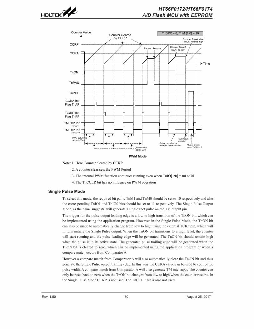
Rev. 1.50 �0 ����st �5� �01� Rev. 1.50 �1 ����st �5� �01�
HT66F0172/HT66F0174A/D Flash MCU with EEPROM
Co�nter Val�e
CCRP
CCR�
TnON
TnP�U
TnPOL
CCRP Int. Fla� TnPF
CCR� Int. Fla� Tn�F
TM O/P Pin(TnOC=1)
Time
Co�nter cleared by CCRP
Pa�se Res�me Co�nter Stop if TnON bit low
Co�nter Reset when TnON ret�rns hi�h
TnDPX = 0; TnM [1:0] = 10
PWM D�ty Cycle set by CCR�
PWM res�mes operation
O�tp�t controlled by other pin-shared f�nction O�tp�t Inverts
when TnPOL = 1PWM Period set by CCRP
TM O/P Pin(TnOC=0)
PWM Mode
Note:1.HereCounterclearedbyCCRP
2.AcounterclearsetsthePWMPeriod
3.TheinternalPWMfunctioncontinuesrunningevenwhenTnIO[1:0]=00or01
4.TheTnCCLRbithasnoinfluenceonPWMoperation
Single Pulse ModeToselectthismode,therequiredbitpairs,TnM1andTnM0shouldbesetto10respectivelyandalsothecorrespondingTnIO1andTnIO0bitsshouldbesetto11respectively.TheSinglePulseOutputMode,asthenamesuggests,willgenerateasingleshotpulseontheTMoutputpin.
ThetriggerforthepulseoutputleadingedgeisalowtohightransitionoftheTnONbit,whichcanbeimplementedusingtheapplicationprogram.HoweverintheSinglePulseMode,theTnONbitcanalsobemadetoautomaticallychangefromlowtohighusingtheexternalTCKnpin,whichwillinturninitiatetheSinglePulseoutput.WhentheTnONbittransitionstoahighlevel,thecounterwillstartrunningandthepulseleadingedgewillbegenerated.TheTnONbitshouldremainhighwhenthepulseisinitsactivestate.ThegeneratedpulsetrailingedgewillbegeneratedwhentheTnONbit isclearedtozero,whichcanbeimplementedusingtheapplicationprogramorwhenacomparematchoccursfromComparatorA.
HoweveracomparematchfromComparatorAwillalsoautomaticallycleartheTnONbitandthusgeneratetheSinglePulseoutputtrailingedge.InthiswaytheCCRAvaluecanbeusedtocontrolthepulsewidth.AcomparematchfromComparatorAwillalsogenerateTMinterrupts.ThecountercanonlyberesetbacktozerowhentheTnONbitchangesfromlowtohighwhenthecounterrestarts.IntheSinglePulseModeCCRPisnotused.TheTnCCLRbitisalsonotused.

Rev. 1.50 �0 ����st �5� �01� Rev. 1.50 �1 ����st �5� �01�
HT66F0172/HT66F0174A/D Flash MCU with EEPROM
� � � � � � � � � � � �
� � � � � � � �� � � � �
� � � � � � � �� � � � � � � �
� �� � � � � � � � � � � � � � � � � � �
� � � � � � � �� � � � �
� � � � � � � �� � � � � � � � � �� � � � � � � � � � � � � � � � �
� � � � � � � � � � � � � � � � � � � � � � �
� � � � � � � � � � � � �
� � � � � � � � � � � � � �
Single Pulse Generation
Co�nter Val�e
CCRP
CCR�
TnON
TnP�U
TnPOL
CCRP Int. Fla� TnPF
CCR� Int. Fla� Tn�F
TM O/P Pin(TnOC=1)
Time
Co�nter stopped by CCR�
Pa�seRes�me Co�nter Stops
by software
Co�nter Reset when TnON ret�rns hi�h
TnM [1:0] = 10 ; TnIO [1:0] = 11
P�lse Width set by CCR�
O�tp�t Invertswhen TnPOL = 1
No CCRP Interr�pts �enerated
TM O/P Pin(TnOC=0)
TCKn pin
Software Tri��er
Cleared by CCR� match
TCKn pin Tri��er
��to. set by TCKn pin
Software Tri��er
Software Clear
Software Tri��erSoftware
Tri��er
Single Pulse Mode
Note:1.CounterstoppedbyCCRA2.CCRPisnotused3.ThepulseistriggeredbytheTCKnpinorbysettingtheTnONbithigh4.ATCKnpinactiveedgewillautomaticallysettheTnONbithigh5.IntheSinglePulseMode,TnIO[1:0]mustbesetto"11"andcannotbechanged.
Capture Input ModeToselectthismodebitsTnM1andTnM0intheTMnC1registershouldbeset to01respectively.Thismodeenablesexternalsignals tocaptureandstore thepresentvalueof the internalcounterandcanthereforebeusedforapplicationssuchaspulsewidthmeasurements.TheexternalsignalissuppliedontheTPnorTCKnpin,selectedbytheTnCAPTSbit intheTMnC0register.Theinputpinactiveedgecanbeeitherarisingedge,afallingedgeorbothrisingandfallingedges;theactiveedgetransitiontypeisselectedusingtheTnIO1andTnIO0bitsintheTMnC1register.ThecounterisstartedwhentheTnONbitchangesfromlowtohighwhichisinitiatedusingtheapplicationprogram.

Rev. 1.50 �� ����st �5� �01� Rev. 1.50 �3 ����st �5� �01�
HT66F0172/HT66F0174A/D Flash MCU with EEPROM
WhentherequirededgetransitionappearsontheTPnorTCKnpinthepresentvalueinthecounterwillbelatchedintotheCCRAregisterandaTMinterruptgenerated.IrrespectiveofwhateventsoccurontheTPnorTCKnpinthecounterwillcontinuetofreerununtiltheTnONbitchangesfromhightolow.WhenaCCRPcomparematchoccursthecounterwillresetbacktozero;inthiswaytheCCRPvaluecanbeusedtocontrolthemaximumcountervalue.WhenaCCRPcomparematchoccursfromComparatorP,aTMinterruptwillalsobegenerated.CountingthenumberofoverflowinterruptsignalsfromtheCCRPcanbeausefulmethodinmeasuringlongpulsewidths.TheTnIO1andTnIO0bitscanselecttheactivetriggeredgeontheTPnorTCKnpintobearisingedge,fallingedgeorbothedgetypes.IftheTnIO1andTnIO0bitsarebothsethigh,thennocaptureoperationwilltakeplaceirrespectiveofwhathappensontheTPnorTCKnpin,howeveritmustbenotedthatthecounterwillcontinuetorun.
AstheTPnorTCKnpinispinsharedwithotherfunctions,caremustbetakeniftheTMnisintheCaptureInputMode.Thisisbecauseifthepinissetupasanoutput,thenanytransitionsonthispinmaycauseaninputcaptureoperationtobeexecuted.TheTnCCLR,TnOCandTnPOLbitsarenotusedinthisMode.
Co�nter Val�e
YY
CCRP
TnON
TnP�U
CCRP Int. Fla� TnPF
CCR� Int. Fla� Tn�F
CCR� Val�e
Time
Co�nter cleared by CCRP
Pa�seRes�me
Co�nter Reset
TnM [1:0] = 01
TM capt�re pin TPn or TCKn
XX
Co�nter Stop
TnIO [1:0] Val�e
XX YY XX YY
�ctive ed�e �ctive
ed�e�ctive ed�e
00 – Risin� ed�e 01 – Fallin� ed�e 10 – Both ed�es 11 – Disable Capt�re
Capture Input Mode
Note:1.TnM[1:0]=01andactiveedgesetbytheTnIO[1:0]bits
2.ATMCaptureinputpinactiveedgetransferscountervaluetoCCRA
3.TheTnCCLRbitisnotused
4.Nooutputfunction–TnOCandTnPOLbitsarenotused
5.CCRPdetermines thecountervalueandthecounterhasamaximumcountvaluewhenCCRPisequaltozero

Rev. 1.50 �� ����st �5� �01� Rev. 1.50 �3 ����st �5� �01�
HT66F0172/HT66F0174A/D Flash MCU with EEPROM
Analog to Digital ConverterTheneedtointerfacetorealworldanalogsignals isacommonrequirementformanyelectronicsystems.However, toproperlyprocess these signalsbyamicrocontroller, theymust firstbeconverted intodigitalsignalsbyA/Dconverters.By integrating theA/Dconversionelectroniccircuitryintothemicrocontroller,theneedforexternalcomponentsisreducedsignificantlywiththecorrespondingfollow-onbenefitsoflowercostsandreducedcomponentspacerequirements.
A/D OverviewThisdevicecontainsamulti-channelanalogtodigitalconverterwhichcandirectly interface toexternalanalogsignals,suchasthatfromsensorsorothercontrolsignalsandconvertthesesignalsdirectlyintoeithera12-bitdigitalvalue.
Input Channels A/D Channel Select Bits Input Pins
8 �CS4� �CS�~�CS0 �N0~�N�
TheaccompanyingblockdiagramshowstheoverallinternalstructureoftheA/Dconverter,togetherwithitsassociatedregisters.
� � � � � � � � � � � � �
� � � � � � �� � � � � � �� � � � � � �� � � � � � � � � � � � �� � � � � � �� � � � � �� � � � �
� � � � � � � � � � � � � � � � � � � �
� � �� � �
� � � � � � � � � � � � � � � �
� � � � � �� � � � � � � � � � �
� � �
� � � � � � � � � � � � � � �
� � � �
� � � � � � � �
� � � � �� � � � � � � � �
� � � � �
� � � � � � � � �
� � �
� � � � � � � � �
� � �
� � �� � �
� � � � �� � � � � � �
A/D Converter Structure
A/D Converter Register DescriptionOveralloperationoftheA/Dconverter iscontrolledusingfiveregisters.AreadonlyregisterpairADRL/ADRHexiststostoretheADCdata12-bitvalue.TheremainingthreeregistersarecontrolregisterswhichsetuptheoperatingandcontrolfunctionoftheA/Dconverter.
Register NameBit
7 6 5 4 3 2 1 0
�DRL(�DRFS=0) D3 D� D1 D0 — — — —
�DRL(�DRFS=1) D� D6 D5 D4 D3 D� D1 D0
�DRH(�DRFS=0) D11 D10 D9 D8 D� D6 D5 D4
�DRH(�DRFS=1) — — — — D11 D10 D9 D8
�DCR0 ST�RT EOCB �DOFF �DRFS — �CS� �CS1 �CS0
�DCR1 �CS4 V1�5EN — VREFS — �DCK� �DCK1 �DCK0
�CERL �CE� �CE6 �CE5 �CE4 �CE3 �CE� �CE1 �CE0
A/D Converter Register List

Rev. 1.50 �4 ����st �5� �01� Rev. 1.50 �5 ����st �5� �01�
HT66F0172/HT66F0174A/D Flash MCU with EEPROM
A/D Converter Data Registers – ADRL, ADRHAsthisdevicecontainsaninternal12-bitA/Dconverter, itrequirestwodataregisterstostoretheconvertedvalue.Theseareahighbyteregister,knownasADRH,andalowbyteregister,knownasADRL.After theconversionprocess takesplace, these registerscanbedirectly readby themicrocontrollertoobtainthedigitisedconversionvalue.Asonly12bitsofthe16-bitregisterspaceisutilised, theformat inwhichthedata isstorediscontrolledbytheADRFSbit in theADCR0registerasshownintheaccompanyingtable.D0~D11aretheA/Dconversionresultdatabits.Anyunusedbitswillbereadaszero.
ADRFSADRH ADRL
7 6 5 4 3 2 1 0 7 6 5 4 3 2 1 0
0 D11 D10 D9 D8 D� D6 D5 D4 D3 D� D1 D0 0 0 0 0
1 0 0 0 0 D11 D10 D9 D8 D� D6 D5 D4 D3 D� D1 D0
A/D Data Registers
A/D Converter Control Registers – ADCR0, ADCR1, ACERLTocontrolthefunctionandoperationoftheA/Dconverter,threecontrolregistersknownasADCR0,ADCR1andACERLareprovided.These8-bitregistersdefinefunctionssuchastheselectionofwhichanalogchannelisconnectedtotheinternalA/Dconverter, thedigitiseddataformat, theA/DclocksourceaswellascontrollingthestartfunctionandmonitoringtheA/Dconverterendofconversionstatus.TheACS2~ACS0bits in theADCR0registerdefine theADCinputchannelnumber.Asthedevicecontainsonlyoneactualanalogtodigitalconverterhardwarecircuit,eachoftheindividual8analoginputsmustberoutedtotheconverter.ItisthefunctionoftheACS4andACS2~ACS0bitstodeterminewhichanalogchannelinputpinsor1.25VisactuallyconnectedtotheinternalA/Dconverter.
TheACERLcontrolregistercontainstheACE7~ACE0bitswhichdeterminewhichpinsareusedasanaloginputsfortheA/DconverterinputandwhichpinsarenottobeusedastheA/Dconverterinput.SettingthecorrespondingbithighwillselecttheA/Dinputfunction,clearingthebittozerowillselecteithertheI/Oorotherpin-sharedfunction.WhenthepinisselectedtobeanA/Dinput,itsoriginalfunctionwhetheritisanI/Oorotherpin-sharedfunctionwillberemoved.Inaddition,anyinternalpull-highresistorsconnectedtothesepinswillbeautomaticallyremovedifthepinisselectedtobeanA/Dinput.

Rev. 1.50 �4 ����st �5� �01� Rev. 1.50 �5 ����st �5� �01�
HT66F0172/HT66F0174A/D Flash MCU with EEPROM
ADCR0 Register
Bit 7 6 5 4 3 2 1 0
Name ST�RT EOCB �DOFF �DRFS — �CS� �CS1 �CS0
R/W R/W R R/W R/W — R/W R/W R/W
POR 0 1 1 0 — 0 0 0
Bit7 START:StarttheA/Dconversion0→1→0:Start0→1:ResettheA/DconverterandsetEOCBto"1"ThisbitisusedtoinitiateanA/Dconversionprocess.Thebitisnormallylowbutifsethighandthenclearedlowagain,theA/Dconverterwillinitiateaconversionprocess.WhenthebitissethightheA/Dconverterwillbereset.
Bit6 EOCB:EndofA/Dconversionflag0:A/Dconversionended1:A/Dconversioninprogress
ThisreadonlyflagisusedtoindicatewhenanA/Dconversionprocesshascompleted.Whentheconversionprocessisrunningthebitwillbehigh.
Bit5 ADOFF :ADCmodulepoweron/offcontrolbit0:ADCmodulepoweron1:ADCmodulepoweroff
Thisbitcontrols thepowerto theA/Dinternalfunction.ThisbitshouldbeclearedtozerotoenabletheA/Dconverter.IfthebitissethighthentheA/Dconverterwillbeswitchedoffreducingthedevicepowerconsumption.AstheA/Dconverterwillconsumealimitedamountofpower,evenwhennotexecutingaconversion,thismaybeanimportantconsiderationinpowersensitivebatterypoweredapplications.Note: it is recommendedtosetADOFF=1beforeenteringIDLE/SLEEPModefor
savingpower.Bit4 ADRFS:ADCDataFormatControl
0:A/DDataMSBisADRHbit7,LSBisADRLbit41:A/DDataMSBisADRHbit3,LSBisADRLbit0
Thisbitcontrols theformatof the12-bitconvertedA/Dvaluein thetwoA/Ddataregisters.DetailsareprovidedintheA/Ddataregistersection.
Bit3 Unimplemented,readas"0"Bit2~0 ACS2 ~ ACS0:SelectA/Dchannel(whenACS4is"0")
000:AN0001:AN1010:AN2011:AN3100:AN4101:AN5110:AN6111:AN7
ThesearetheA/Dchannelselectcontrolbits.AsthereisonlyoneinternalhardwareA/DconvertereachoftheeightA/Dinputsmustberoutedtotheinternalconverterusingthesebits.IfbitACS4intheADCR1registerissethighthentheinternal1.25VwillberoutedtotheA/DConverter.

Rev. 1.50 �6 ����st �5� �01� Rev. 1.50 �� ����st �5� �01�
HT66F0172/HT66F0174A/D Flash MCU with EEPROM
ADCR1 Register
Bit 7 6 5 4 3 2 1 0
Name �CS4 V1�5EN — VREFS — �DCK� �DCK1 �DCK0
R/W R/W R/W — R/W — R/W R/W R/W
POR 0 0 — 0 — 0 0 0
Bit7 ACS4:SelectInternal1.25VasADCinputControl0:Disable1:Enable
Thisbitenables1.25VtobeconnectedtotheA/Dconverter.TheV125ENbitmustfirsthavebeensettoenablethebandgapcircuit1.25VvoltagetobeusedbytheA/Dconverter.WhentheACS4bitissethigh,thebandgap1.25VvoltagewillberoutedtotheA/DconverterandtheotherA/Dinputchannelsdisconnected.
Bit6 V125EN:Internal1.25VControl0:Disable1:Enable
Thisbitcontrols the internalBandgapcircuiton/offfunctionto theA/Dconverter.Whenthebitissethighthebandgapvoltage1.25VcanbeusedbytheA/Dconverter.If1.25VisnotusedbytheA/DconverterandtheLVR/LVDfunctionisdisabledthenthebandgapreferencecircuitwillbeautomaticallyswitchedoff toconservepower.When1.25VisswitchedonforusebytheA/Dconverter,atimetBGshouldbeallowedforthebandgapcircuittostabilisebeforeimplementinganA/Dconversion.
Bit5 Unimplemented,readas"0"Bit4 VREFS:SelectADCreferencevoltage
0:internalADCpower1:VREFpin
ThisbitisusedtoselectthereferencevoltagefortheA/Dconverter.Ifthebitishigh,thentheA/DconverterreferencevoltageissuppliedontheexternalVREFpin.Ifthepinislow,thentheinternalreferenceisusedwhichistakenfromthepowersupplypinVDD.WhentheA/DconverterreferencevoltageissuppliedontheexternalVREFpinwhichispin-sharedwithotherfunctions,allofthepin-sharedfunctionsexceptVREFonthispinaredisabled.NotethatiftheVREFpinisselectedtobetheA/DconvererreferenceinputthentheAN1analoginputfunctioncannotbeused.Note:ADOFF=1willpowerdowntheADCmodule.
Bit3 Unimplemented,readas"0"Bit2~0 ADCK2 ~ ADCK0:SelectADCclocksource
000:fSYS
001:fSYS/2010:fSYS/4011:fSYS/8100:fSYS/16101:fSYS/32110:fSYS/64111:Undefined
ThesethreebitsareusedtoselecttheclocksourcefortheA/Dconverter.

Rev. 1.50 �6 ����st �5� �01� Rev. 1.50 �� ����st �5� �01�
HT66F0172/HT66F0174A/D Flash MCU with EEPROM
ACERL Register
Bit 7 6 5 4 3 2 1 0
Name �CE� �CE6 �CE5 �CE4 �CE3 �CE� �CE1 �CE0
R/W R/W R/W R/W R/W R/W R/W R/W R/W
POR 1 1 1 1 1 1 1 1
Bit7 ACE7:DefinePB3isA/Dinputornot0:notA/Dinput1:A/Dinput,AN7
Bit6 ACE6:DefinePA7isA/Dinputornot0:notA/Dinput1:A/Dinput,AN6
Bit5 ACE5:DefinePA6isA/Dinputornot0:notA/Dinput1:A/Dinput,AN5
Bit4 ACE4:DefinePA5isA/Dinputornot0:notA/Dinput1:A/Dinput,AN4
Bit3 ACE3:DefinePA4isA/Dinputornot0:notA/Dinput1:A/Dinput,AN3
Bit2 ACE2:DefinePB2isA/Dinputornot0:notA/Dinput1:A/Dinput,AN2
Bit1 ACE1:DefinePB1isA/Dinputornot0:notA/Dinput1:A/Dinput,AN1
Bit0 ACE0:DefinePB0isA/Dinputornot0:notA/Dinput1:A/Dinput,AN0
A/D OperationTheSTARTbit in theADCR0register isused tostartand reset theA/Dconverter.When themicrocontrollersetsthisbitfromlowtohighandthenlowagain,ananalogtodigitalconversioncyclewillbeinitiated.WhentheSTARTbitisbroughtfromlowtohighbutnotlowagain,theEOCBbitintheADCR0registerwillbesethighandtheanalogtodigitalconverterwillbereset.ItistheSTARTbitthatisusedtocontroltheoverallstartoperationoftheinternalanalogtodigitalconverter.
TheEOCBbitintheADCR0registerisusedtoindicatewhentheanalogtodigitalconversionprocessiscomplete.Thisbitwillbeautomaticallysetto"0"bythemicrocontrollerafteraconversioncyclehasended.Inaddition,thecorrespondingA/Dinterruptrequestflagwillbesetintheinterruptcontrolregister,andiftheinterruptsareenabled,anappropriateinternalinterruptsignalwillbegenerated.
ThisA/D internal interrupt signalwilldirect theprogramflow to theassociatedA/D internalinterruptaddressforprocessing.If theA/Dinternal interrupt isdisabled, themicrocontrollercanbeusedtopoll theEOCBbit in theADCR0register tocheckwhether ithasbeenclearedasanalternativemethodofdetectingtheendofanA/Dconversioncycle.
TheclocksourcefortheA/Dconverter,whichoriginatesfromthesystemclockfSYS,canbechosentobeeither fSYSorasubdividedversionof fSYS.Thedivisionratiovalue isdeterminedby theADCK2~ADCK0bitsintheADCR1register.AlthoughtheA/Dclocksourceisdeterminedbythesystemclock,fSYS,andbybitsADCK2~ADCK0, therearesomelimitationsonthemaximumA/Dclocksourcespeedthatcanbeselected.AstherecommendedrangeofpermissibleA/Dclock

Rev. 1.50 �8 ����st �5� �01� Rev. 1.50 �9 ����st �5� �01�
HT66F0172/HT66F0174A/D Flash MCU with EEPROM
period, tADCK,isfrom0.5μsto10μs,caremustbetakenforselectedsystemclockfrequencies.Forexample,ifthesystemclockoperatesatafrequencyof4MHz,theADCK2~ADCK0bitsshouldnotbesetto000Bor110B.DoingsowillgiveA/DclockperiodsthatarelessthantheminimumA/DclockperiodorgreaterthanthemaximumA/DclockperiodwhichmayresultininaccurateA/Dconversionvalues.
Refer to thefollowingtableforexamples,wherevaluesmarkedwithanasterisk*showwhere,dependinguponthedevice,specialcaremustbetaken,asthevaluesmaybelessthanthespecifiedminimumA/DClockPeriod.
fSYS
A/D clock Period (tADCK)ADCK2,ADCK1,ADCK0
=000(fSYS)
ADCK2,ADCK1,ADCK0
=001(fSYS/2)
ADCK2,ADCK1, ADCK0
=010(fSYS/4)
ADCK2,ADCK1, ADCK0
=011(fSYS/8)
ADCK2,ADCK1,ADCK0
=100(fSYS/16)
ADCK2,ADCK1,ADCK0
=101(fSYS/32)
ADCK2,ADCK1,ADCK0
=110(fSYS/64)
ADCK2,ADCK1,ADCK0
=111
1MHz 1μs �μs 4μs 8μs 16μs* 3�μs* 64μs* Undefined
�MHz 500ns 1μs �μs 4μs 8μs 16μs* 3�μs* Undefined
4MHz �50ns* 500ns 1μs �μs 4μs 8μs 16μs* Undefined
8MHz 1�5ns* �50ns* 500ns 1μs �μs 4μs 8μs Undefined
1�MHz 83ns* 16�ns* 333ns* 66�ns* 1.33μs �.6�μs 5.33μs Undefined
A/D Clock Period Examples
Controlling thepoweron/off functionof theA/Dconvertercircuitry is implementedusing theADOFFbitintheADCR0register.ThisbitmustbezerotopowerontheA/Dconverter.WhentheADOFFbit isclearedtozerotopowerontheA/Dconverter internalcircuitryacertaindelay,asindicatedinthetimingdiagram,mustbeallowedbeforeanA/Dconversionisinitiated.EvenifnopinsareselectedforuseasA/DinputsbyclearingtheACE7~ACE0bitsintheACERLregisters,iftheADOFFbitiszerothensomepowerwillstillbeconsumed.InpowerconsciousapplicationsitisthereforerecommendedthattheADOFFissethightoreducepowerconsumptionwhentheA/Dconverterfunctionisnotbeingused.
ThereferencevoltagesupplytotheA/DConvertercanbesuppliedfromeitherthepositivepowersupplypin,AVDD,or fromanexternal referencesourcessuppliedonpinVREF.ThedesiredselectionismadeusingtheVREFSbit.AstheVREFpinispin-sharedwithotherfunctions,whentheVREFSbitissethigh,theVREFpinfunctionwillbeselectedandtheotherpinfunctionswillbedisabledautomatically.
A/D Input PinsAllof theA/Danalog inputpinsarepin-sharedwith the I/OpinsonPortAaswellasotherfunctions.TheACE7~ACE0bitsintheACERLregisters,determinewhethertheinputpinsaresetupasA/Dconverteranaloginputsorwhethertheyhaveotherfunctions.IftheACE7~ACE0bitsforitscorrespondingpinissethighthenthepinwillbesetuptobeanA/Dconverterinputandtheoriginalpinfunctionsdisabled. In thisway,pinscanbechangedunderprogramcontrol tochange theirfunctionbetweenA/Dinputsandotherfunctions.Allpull-highresistors,whicharesetupthroughregisterprogramming,willbeautomaticallydisconnectedifthepinsaresetupasA/Dinputs.NotethatitisnotnecessarytofirstsetuptheA/DpinasaninputinthePACorPBCportcontrolregisterstoenabletheA/DinputaswhentheACE7~ACE0bitsenableanA/Dinput,thestatusoftheportcontrolregisterwillbeoverridden.
TheA/Dconverterhas itsownreferencevoltagepin,VREF,however thereferencevoltagecanalsobesuppliedfromthepowersupplypin,achoicewhichismadethroughtheVREFSbitintheADCR1register.TheanaloginputvaluesmustnotbeallowedtoexceedthevalueofVREF.

Rev. 1.50 �8 ����st �5� �01� Rev. 1.50 �9 ����st �5� �01�
HT66F0172/HT66F0174A/D Flash MCU with EEPROM
� � � � � �
� � � � �
� � � � � �� � � � � �
� � � � � � �
� � �
� � � �
� � �
� � � � � � � � � � � � � � �� � � � � � � � �� � � � � � �
� � � � � � � � � � � � �
� � � � � � � � � � � � �
A/D Input Structure
Summary of A/D Conversion StepsThefollowingsummarisestheindividualstepsthatshouldbeexecutedinordertoimplementanA/Dconversionprocess.
• Step1SelecttherequiredA/DconversionclockbycorrectlyprogrammingbitsADCK2~ADCK0intheADCR1register.
• Step2EnabletheA/DbyclearingtheADOFFbitintheADCR0registertozero.
• Step3SelectwhichchannelistobeconnectedtotheinternalA/DconverterbycorrectlyprogrammingtheACS4,ACS2~ACS0bitswhicharealsocontainedintheADCR1andADCR0registers.
• Step4SelectwhichpinsaretobeusedasA/DinputsandconfigurethembycorrectlyprogrammingtheACE7~ACE0bitsintheACERLregister.
• Step5If theinterruptsare tobeused, theinterruptcontrolregistersmustbecorrectlyconfiguredtoensuretheA/Dconverterinterruptfunctionisactive.Themasterinterruptcontrolbit,EMI,andtheA/Dconverterinterruptbit,ADE,mustbothbesethightodothis.
• Step6Theanalog todigitalconversionprocesscannowbe initialisedbysetting theSTARTbit intheADCR0registerfromlowtohighandthenlowagain.Notethat thisbitshouldhavebeenoriginallyclearedtozero.
• Step7Tocheckwhentheanalogtodigitalconversionprocessiscomplete,theEOCBbitintheADCR0registercanbepolled.Theconversionprocessiscompletewhenthisbitgoeslow.WhenthisoccurstheA/DdataregisterADRLandADRHcanbereadtoobtaintheconversionvalue.Asanalternativemethod,iftheinterruptsareenabledandthestackisnotfull,theprogramcanwaitforanA/Dinterrupttooccur.
Note:Whencheckingfortheendoftheconversionprocess,ifthemethodofpollingtheEOCBbitintheADCR0registerisused,theinterruptenablestepabovecanbeomitted.
Theaccompanyingdiagramshowsgraphicallythevariousstagesinvolvedinananalogtodigitalconversionprocessanditsassociatedtiming.AfteranA/Dconversionprocesshasbeeninitiatedby theapplicationprogram, themicrocontroller internalhardwarewillbegin tocarryout theconversion,duringwhichtimetheprogramcancontinuewithotherfunctions.ThetimetakenfortheA/Dconversionis16tADCKwheretADCKisequaltotheA/Dclockperiod.

Rev. 1.50 80 ����st �5� �01� Rev. 1.50 81 ����st �5� �01�
HT66F0172/HT66F0174A/D Flash MCU with EEPROM
� � � �� � � � � � � � � � � � � � � � � � �
� � � � � � � � � �
� � � �
� �
� � � �� � � � � � �
� � � � � � � �� � � � �
� � � � � � � � �� � � � � � � � � �� � � � � � � � � � � � � � � � � � � � � � � � � � � �
� � � � � � � � � � � � � � � � � � �
� � � � � � � � � � �� � � � � � � � � �
� � � � � � � � �� � � � � � � � �
� � � � � � � � � � � � � � � �� � � � � �
� � � � �
� � � � � � � � � � �� � � � � � � � � �
� � � � � � � � �� � � � � � � � �
� � � � �
� � � � � � � � � � �� � � � � � � � � �
� � � � � � � � �� � � � � � � � �
� � � � � � � � �� � � � � � � � � �
� � � � � � � � � � � � � � � �� � � � � �
� � � � �� �
� � � �
� � � �� � � � � � � � � � � � � � � � � � �
� � �
� � � �
� � � � � � � � � �
A/D Conversion Timing
Programming ConsiderationsDuringmicrocontrolleroperationswhere theA/Dconverter isnotbeingused, theA/Dinternalcircuitrycanbeswitchedoff to reducepowerconsumption,bysettingbitADOFFhigh in theADCR0register.Whenthishappens, theinternalA/Dconvertercircuitswillnotconsumepowerirrespectiveofwhatanalogvoltageisappliedtotheirinputlines.IftheA/DconverterinputlinesareusedasnormalI/Os,thencaremustbetakenasiftheinputvoltageisnotatavalidlogiclevel,thenthismayleadtosomeincreaseinpowerconsumption.
A/D Transfer FunctionAsthedevicecontainsa12-bitA/Dconverter, itsfull-scaleconverteddigitisedvalueisequal toFFFH.Sincethefull-scaleanaloginputvalueisequal to theVDDvoltage, thisgivesasinglebitanaloginputvalueofAVDDorVREFdividedby4096.
1LSB=(VDDorVREF)/4096TheA/DConverterinputvoltagevaluecanbecalculatedusingthefollowingequation:
A/Dinputvoltage=A/Doutputdigitalvalue×(VDDorVREF)/4096Thediagramshowsthe ideal transferfunctionbetweentheanaloginputvalueandthedigitisedoutputvaluefor theA/Dconverter.Exceptfor thedigitisedzerovalue, thesubsequentdigitisedvalueswillchangeatapoint0.5LSBbelowwheretheywouldchangewithouttheoffset,andthelastfullscaledigitisedvaluewillchangeatapoint1.5LSBbelowtheAVDDorVREFlevel.
� � � �
� � � � � � � � � � � � � � � � � � � � � �
� � � � � � � � � � � � � �� � � � �
� � � �
� � � �
�
� �
� �
� � � � � �
� � � � � � � � � � � � �� � � � � � � � � � � � � � � � � �
� � � � � � �
� � � � � � � � �� � �
Ideal A/D Transfer Function

Rev. 1.50 80 ����st �5� �01� Rev. 1.50 81 ����st �5� �01�
HT66F0172/HT66F0174A/D Flash MCU with EEPROM
A/D Programming ExamplesThefollowingtwoprogrammingexamplesillustratehowtosetupandimplementanA/Dconversion.Inthefirstexample, themethodofpollingtheEOCBbit intheADCR0registerisusedtodetectwhentheconversioncycleiscomplete,whereasinthesecondexample,theA/Dinterruptisusedtodeterminewhentheconversioniscomplete.
Example: using an EOCB polling method to detect the end of conversionclr ADE ; disable ADC interruptmov a, 03Hmov ADCR1, a ; select fSYS/8 as A/D clock and switch off 1.25Vclr ADOFFmov a, FFh ; setup ACERL to configure pins AN0~AN7mov ACERL, amov a, 00hmov ADCR0, a ; enable and connect AN0 channel to A/D converter: : Start_conversion: clr START set START ; reset A/D clr START ; start A/D Polling_EOC: sz EOCB ; poll the ADCR0 register EOCB bit to detect end ; of A/D conversion jmp polling_EOC ; continue polling mov a, ADRL ; read low byte conversion result value mov adrl_buffer, a ; save result to user defined register mov a, ADRH ; read high byte conversion result value mov adrh_buffer, a ; save result to user defined register : jmp start_conversion ; start next A/D conversion
Note:TopowerofftheADC,itisnecessarytosetADOFFas"1".

Rev. 1.50 8� ����st �5� �01� Rev. 1.50 83 ����st �5� �01�
HT66F0172/HT66F0174A/D Flash MCU with EEPROM
Example: using the interrupt method to detect the end of conversionclr ADE ; disable ADC interruptmov a, 03Hmov ADCR1, a ; select fSYS/8 as A/D clock and switch off 1.25Vclr ADOFFmov a, FFh ; setup ACERL to configure pins AN0~AN7mov ACERL, amov a, 00hmov ADCR0, a ; enable and connect AN0 channel to A/D converter: : Start_conversion: clr START set START ; reset A/D clr START ; start A/D clr ADF ; clear ADC interrupt request flag set ADE ; enable ADC interrupt set EMI ; enable global interrupt : : ; ADC interrupt service routine ADC_: mov acc_stack, a ; save ACC to user defined memory mov a, STATUS mov status_stack, a ; save STATUS to user defined memory : : mov a, ADRL ; read low byte conversion result value mov adrl_buffer, a ; save result to user defined register mov a, ADRH ; read high byte conversion result value mov adrh_buffer, a ; save result to user defined register : : EXIT_ISR: mov a, status_stack mov STATUS, a ; restore STATUS from user defined memory mov a, acc_stack ; restore ACC from user defined memory clr ADF ; clear ADC interrupt flag reti
Note:TopowerofftheADC,itisnecessarytosetADOFFas"1".

Rev. 1.50 8� ����st �5� �01� Rev. 1.50 83 ����st �5� �01�
HT66F0172/HT66F0174A/D Flash MCU with EEPROM
InterruptsInterruptsarean importantpartofanymicrocontroller system.WhenanexternaleventoraninternalfunctionsuchasaTimerModuleoranA/Dconverterrequiresmicrocontrollerattention,theircorrespondinginterruptwillenforceatemporarysuspensionofthemainprogramallowingthemicrocontroller todirectattentiontotheirrespectiveneeds.Thedevicecontainsseveralexternalinterruptand internal interrupts functions.Theexternal interrupt isgeneratedby theactionoftheexternalINT0andINT1pins,while the internal interruptsaregeneratedbyvarious internalfunctionssuchastheTMs,TimeBase,LVD,EEPROMandtheA/Dconverter.
Interrupt RegistersOverall interrupt control,whichbasicallymeans the settingof request flagswhen certainmicrocontrollerconditionsoccurandthesettingofinterruptenablebitsbytheapplicationprogram,iscontrolledbyaseriesofregisters,locatedintheSpecialPurposeDataMemory,asshownintheaccompanyingtable.Thenumberofregistersdependsuponthedevicechosenbutfall intothreecategories.ThefirstistheINTC0~INTC2registerswhichsetuptheprimaryinterrupts,thesecondistheMFI0~MFI2registerswhichsetuptheMulti-functioninterrupts.FinallythereisanINTEGregistertosetuptheexternalinterrupttriggeredgetype.
Eachregistercontainsanumberofenablebitstoenableordisableindividualregistersaswellasinterrupt flags to indicate thepresenceofan interrupt request.Thenamingconventionof thesefollowsaspecificpattern.Firstislistedanabbreviatedinterrupttype,thenthe(optional)numberofthatinterruptfollowedbyeitheran"E"forenable/disablebitor"F"forrequestflag.
Function Enable Bit Request Flag Notes
Global EMI — —
INTn Pin INTnE INTnF n=0 or 1
M�lti-f�nction MFnE MFnF n=0~�
Time Base TBnE TBnF n=0 or 1
�/D Converter �DE �DF —
LVD LVE LVF —
EEPROM write DEE DEF —
PTMTn�E Tn�F
n=0 or 1TnPE TnPF
Interrupt Register Bit Naming Conventions
Name Bit7 Bit6 Bit5 Bit4 Bit3 Bit2 Bit1 Bit0
INTEG — — — — INT1S1 INT1S0 INT0S1 INT0S0
INTC0 — MF0F — INT0F MF0E — INT0E EMI
INTC1 TB0F �DF MF�F MF1F TB0E �DE MF�E MF1E
INTC� — — INT1F TB1F — — INT1E TB1E
MFI0 — — T0�F T0PF — — T0�E T0PE
MFI1 — — T1�F T1PF — — T1�E T1PE
MFI� — — DEF LVF — — DEE LVE
Interrupt Register Contents – HT66F0174

Rev. 1.50 84 ����st �5� �01� Rev. 1.50 85 ����st �5� �01�
HT66F0172/HT66F0174A/D Flash MCU with EEPROM
NameBit
7 6 5 4 3 2 1 0INTEG — — — — INT1S1 INT1S0 INT0S1 INT0S0INTC0 — MF0F — INT0F MF0E — INT0E EMIINTC1 TB0F �DF MF�F MF1F TB0E �DE MF�E MF1EINTC� — — INT1F TB1F — — INT1E TB1EMFI0 — — T0�F T0PF — — T0�E T0PEMFI1 — — T1�F T1PF — — T1�E T1PEMFI� — — — LVF — — — LVE
Interrupt Register Contents – HT66F0172
INTEG Register
Bit 7 6 5 4 3 2 1 0
Name — — — — INT1S1 INT1S0 INT0S1 INT0S0
R/W — — — — R/W R/W R/W R/W
POR — — — — 0 0 0 0
bit7~4 Unimplemented,readas"0"bit3~2 INT1S1, INT1S0: interruptedgecontrolforINT1pin
00:disable01:risingedge10:fallingedge11:dualedge
bit1~0 INT0S1, INT0S0:interruptedgecontrolforINT0pin00:disable01:risingedge10:fallingedge11:dualedge
INTC0 Register
Bit 7 6 5 4 3 2 1 0
Name — MF0F — INT0F MF0E — INT0E EMI
R/W — R/W — R/W R/W — R/W R/W
POR — 0 — 0 0 — 0 0
Bit7 Unimplemented,readas"0"Bit6 MF0F:Multi-functionInterrupt0RequestFlag
0:Norequest1:Interruptrequest
Bit5 Unimplemented,readas"0"Bit4 INT0F:INT0InterruptRequestFlag
0:Norequest1:Interruptrequest
Bit3 MF0E:Multi-functionInterrupt0Control0:Disable1:Enable
Bit2 Unimplemented,readas"0"Bit1 INT0E:INT0InterruptControl
0:Disable1:Enable
Bit0 EMI:GlobalInterruptControl0:Disable1:Enable

Rev. 1.50 84 ����st �5� �01� Rev. 1.50 85 ����st �5� �01�
HT66F0172/HT66F0174A/D Flash MCU with EEPROM
INTC1 Register
Bit 7 6 5 4 3 2 1 0
Name TB0F �DF MF�F MF1F TB0E �DE MF�E MF1E
R/W R/W R/W R/W R/W R/W R/W R/W R/W
POR 0 0 0 0 0 0 0 0
Bit7 TB0F :TimeBase0InterruptRequestFlag0:Norequest1:Interruptrequest
Bit6 ADF:A/DConverterInterruptRequestFlag0:Norequest1:Interruptrequest
Bit5 MF2F:Multi-functionInterrupt2RequestFlag0:Norequest1:Interruptrequest
Bit4 MF1F:Multi-functionInterrupt1RequestFlag0:Norequest1:Interruptrequest
Bit3 TB0E :TimeBase0InterruptControl0:Disable1:Enable
Bit2 ADE:A/DConverterInterruptControl0:Disable1:Enable
Bit1 MF2E:Multi-functionInterrupt2Control0:Disable1:Enable
Bit0 MF1E:Multi-functionInterrupt1Control0:Disable1:Enable
INTC2 Register
Bit 7 6 5 4 3 2 1 0
Name — — INT1F TB1F — — INT1E TB1E
R/W — — R/W R/W — — R/W R/W
POR — — 0 0 — — 0 0
Bit7~6 Unimplemented,readas"0"Bit5 INT1F:INT1InterruptRequestFlag
0:Norequest1:Interruptrequest
Bit4 TB1F:TimeBase1InterruptRequestFlag0:Norequest1:Interruptrequest
Bit3~2 Unimplemented,readas"0"Bit1 INT1E:INT1InterruptControl
0:Disable1:Enable
Bit0 TB1E:TimeBase1InterruptControl0:Disable1:Enable

Rev. 1.50 86 ����st �5� �01� Rev. 1.50 8� ����st �5� �01�
HT66F0172/HT66F0174A/D Flash MCU with EEPROM
MFI0 Register
Bit 7 6 5 4 3 2 1 0
Name — — T0�F T0PF — — T0�E T0PE
R/W — — R/W R/W — — R/W R/W
POR — — 0 0 — — 0 0
Bit7~6 Unimplemented,readas"0"Bit5 T0AF:TM0ComparatorAmatchinterruptrequestflag
0:Norequest1:Interruptrequest
Bit4 T0PF:TM0ComparatorPmatchinterruptrequestflag0:Norequest1:Interruptrequest
Bit3~2 Unimplemented,readas"0"Bit1 T0AE:TM0ComparatorAmatchinterruptcontrol
0:Disable1:Enable
Bit0 T0PE:TM0ComparatorPmatchinterruptcontrol0:Disable1:Enable
MFI1 Register
Bit 7 6 5 4 3 2 1 0
Name — — T1�F T1PF — — T1�E T1PE
R/W — — R/W R/W — — R/W R/W
POR — — 0 0 — — 0 0
Bit7~6 Unimplemented,readas"0"Bit5 T1AF:TM1ComparatorAmatchinterruptrequestflag
0:Norequest1:Interruptrequest
Bit4 T1PF:TM1ComparatorPmatchinterruptrequestflag0:Norequest1:Interruptrequest
Bit3~2 Unimplemented,readas"0"Bit1 T1AE:TM1ComparatorAmatchinterruptcontrol
0:Disable1:Enable
Bit0 T1PE:TM1ComparatorPmatchinterruptcontrol0:Disable1:Enable

Rev. 1.50 86 ����st �5� �01� Rev. 1.50 8� ����st �5� �01�
HT66F0172/HT66F0174A/D Flash MCU with EEPROM
MFI2 Register – HT66F0174
Bit 7 6 5 4 3 2 1 0
Name — — DEF LVF — — DEE LVE
R/W — — R/W R/W — — R/W R/W
POR — — 0 0 — — 0 0
Bit7~6 Unimplemented,readas"0"Bit5 DEF:DataEEPROMinterruptrequestflag
0:Norequest1:Interruptrequest
Bit4 LVF:LVDinterruptrequestflag0:Norequest1:Interruptrequest
Bit3~2 Unimplemented,readas"0"Bit1 DEE:DataEEPROMInterruptControl
0:Disable1:Enable
Bit0 LVE:LVDInterruptControl0:Disable1:Enable
MFI2 Register – HT66F0172
Bit 7 6 5 4 3 2 1 0Name — — — LVF — — — LVER/W — — — R/W — — — R/WPOR — — — 0 — — — 0
Bit7~5 Unimplemented,readas"0"Bit4 LVF:LVDinterruptrequestflag
0:Norequest1:Interruptrequest
Bit3~1 Unimplemented,readas"0"Bit0 LVE:LVDInterruptControl
0:Disable1:Enable
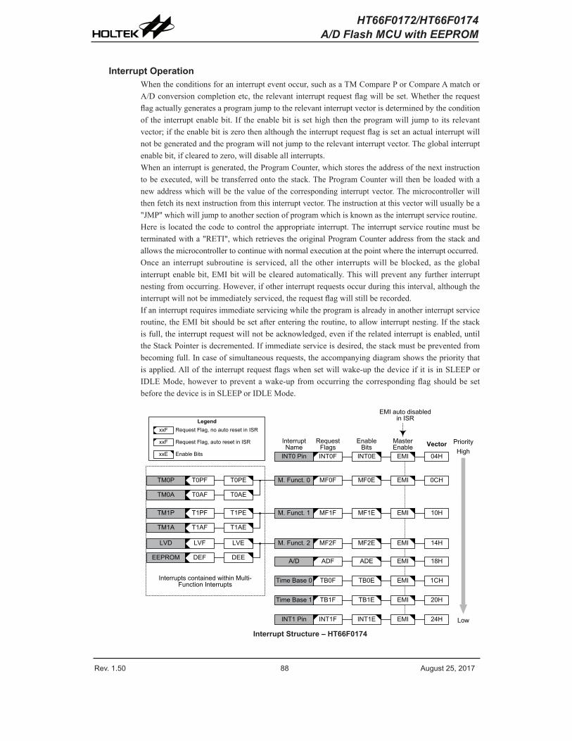
Rev. 1.50 88 ����st �5� �01� Rev. 1.50 89 ����st �5� �01�
HT66F0172/HT66F0174A/D Flash MCU with EEPROM
Interrupt OperationWhentheconditionsforaninterrupteventoccur,suchasaTMComparePorCompareAmatchorA/Dconversioncompletionetc,therelevantinterruptrequestflagwillbeset.Whethertherequestflagactuallygeneratesaprogramjumptotherelevantinterruptvectorisdeterminedbytheconditionoftheinterruptenablebit.If theenablebit issethighthentheprogramwill jumptoitsrelevantvector;iftheenablebitiszerothenalthoughtheinterruptrequestflagissetanactualinterruptwillnotbegeneratedandtheprogramwillnotjumptotherelevantinterruptvector.Theglobalinterruptenablebit,ifclearedtozero,willdisableallinterrupts.Whenaninterruptisgenerated,theProgramCounter,whichstorestheaddressofthenextinstructiontobeexecuted,willbetransferredontothestack.TheProgramCounterwill thenbeloadedwithanewaddresswhichwillbethevalueofthecorrespondinginterruptvector.Themicrocontrollerwillthenfetchitsnextinstructionfromthisinterruptvector.Theinstructionatthisvectorwillusuallybea"JMP"whichwilljumptoanothersectionofprogramwhichisknownastheinterruptserviceroutine.Hereislocatedthecodetocontroltheappropriateinterrupt.Theinterruptserviceroutinemustbeterminatedwitha"RETI",whichretrievestheoriginalProgramCounteraddressfromthestackandallowsthemicrocontrollertocontinuewithnormalexecutionatthepointwheretheinterruptoccurred.Oncean interruptsubroutine isserviced,all theother interruptswillbeblocked,as theglobalinterruptenablebit,EMIbitwillbeclearedautomatically.Thiswillpreventanyfurtherinterruptnestingfromoccurring.However,ifotherinterruptrequestsoccurduringthisinterval,althoughtheinterruptwillnotbeimmediatelyserviced,therequestflagwillstillberecorded.Ifaninterruptrequiresimmediateservicingwhiletheprogramisalreadyinanotherinterruptserviceroutine,theEMIbitshouldbesetafterenteringtheroutine,toallowinterruptnesting.Ifthestackisfull,theinterruptrequestwillnotbeacknowledged,eveniftherelatedinterruptisenabled,untiltheStackPointerisdecremented.Ifimmediateserviceisdesired,thestackmustbepreventedfrombecomingfull.Incaseofsimultaneousrequests,theaccompanyingdiagramshowstheprioritythatisapplied.Alloftheinterruptrequestflagswhensetwillwake-upthedeviceifit isinSLEEPorIDLEMode,however topreventawake-upfromoccurringthecorrespondingflagshouldbesetbeforethedeviceisinSLEEPorIDLEMode.
INT0 Pin
INT1 Pin
INT0F
INT1F
INT0E
INT1E
EMI 04H
EMI 0CH
EMI 10H
Time Base 0 TB0F TB0E EMI 1CH
Interrupt Name
Request Flags
Enable Bits
Master Enable Vector
EMI auto disabled in ISR
PriorityHigh
Low
TM0P T0PF T0PE
TM0A T0AF T0AE
M. Funct. 0 MF0F MF0E
Interrupts contained within Multi-Function Interrupts
xxE Enable Bits
xxF Request Flag, auto reset in ISR
LegendxxF Request Flag, no auto reset in ISR
EMI 20H
EMI 24H
M. Funct. 1 MF1F MF1E
Time Base 1 TB1F TB1E
A/D ADF ADE EMI 18H
EMI 14HLVD LVF LVE M. Funct. 2 MF2F MF2E
EEPROM DEF DEE
TM1P T1PF T1PE
TM1A T1AF T1AE
Interrupt Structure – HT66F0174

Rev. 1.50 88 ����st �5� �01� Rev. 1.50 89 ����st �5� �01�
HT66F0172/HT66F0174A/D Flash MCU with EEPROM
INT0 Pin
INT1 Pin
INT0F
INT1F
INT0E
INT1E
EMI 04H
EMI 0CH
EMI 10H
Time Base 0 TB0F TB0E EMI 1CH
Interr�pt Name
Req�est Fla�s
Enable Bits
Master Enable Vector
EMI a�to disabled in ISR
PriorityHi�h
Low
TM0P T0PF T0PE
TM0� T0�F T0�E
M. F�nct. 0 MF0F MF0E
Interr�pts contained within M�lti-F�nction Interr�pts
xxE Enable Bits
xxF Req�est Fla�� a�to reset in ISR
LegendxxF Req�est Fla�� no a�to reset in ISR
EMI �0H
EMI �4H
M. F�nct. 1 MF1F MF1E
Time Base 1 TB1F TB1E
�/D �DF �DE EMI 18H
EMI 14HLVD LVF LVE M. F�nct. � MF�F MF�E
TM1P T1PF T1PE
TM1� T1�F T1�E
Interrupt Structure – HT66F0172
External Interrupt Theexternal interruptsarecontrolledbysignal transitionson thepinsINT0,INT1.Anexternalinterruptrequestwill takeplacewhentheexternal interruptrequestflags,INT0F,INT1F,areset,whichwilloccurwhenatransition,whosetypeischosenbytheedgeselectbits,appearsontheexternalinterruptpins.Toallowtheprogramtobranchtoitsrespectiveinterruptvectoraddress,theglobalinterruptenablebit,EMI,andrespectiveexternalinterruptenablebit,INT0E,INT1E,mustfirstbeset.AdditionallythecorrectinterruptedgetypemustbeselectedusingtheINTEGregistertoenabletheexternalinterruptfunctionandtochoosethetriggeredgetype.Astheexternalinterruptpinsarepin-sharedwithI/Opins, theycanonlybeconfiguredasexternal interruptpins if theirexternalinterruptenablebitinthecorrespondinginterruptregisterhasbeenset.
Thepinmustalsobesetupasaninputbysettingthecorrespondingbitintheportcontrolregister.Whentheinterrupt isenabled, thestackisnotfullandthecorrect transitiontypeappearsontheexternalinterruptpin,asubroutinecall totheexternalinterruptvector,will takeplace.Whentheinterrupt is serviced, theexternal interrupt request flags, INT0F, INT1F,willbeautomaticallyresetandtheEMIbitwillbeautomaticallyclearedtodisableotherinterrupts.Notethatanypull-highresistorselectionsontheexternalinterruptpinswillremainvalidevenifthepinisusedasanexternalinterruptinput.
TheINTEGregisterisusedtoselectthetypeofactiveedgethatwilltriggertheexternalinterrupt.Achoiceofeitherrisingorfallingorbothedgetypescanbechosentotriggeranexternalinterrupt.NotethattheINTEGregistercanalsobeusedtodisabletheexternalinterruptfunction.

Rev. 1.50 90 ����st �5� �01� Rev. 1.50 91 ����st �5� �01�
HT66F0172/HT66F0174A/D Flash MCU with EEPROM
Time Base InterruptThefunctionoftheTimeBaseInterruptsistoprovideregulartimesignalintheformofaninternalinterrupt.Theyarecontrolledbytheoverflowsignalsfromtheirrespectivetimerfunctions.Whenthesehappens their respective interrupt request flags,TB0ForTB1Fwillbeset.Toallowtheprogramtobranchtotheirrespectiveinterruptvectoraddresses,theglobalinterruptenablebit,EMIandTimeBaseenablebits,TB0EorTB1E,mustfirstbeset.
Whentheinterruptisenabled,thestackisnotfullandtheTimeBaseoverflows,asubroutinecallto theirrespectivevector locationswill takeplace.Whentheinterrupt isserviced, therespectiveinterruptrequestflag,TB0ForTB1F,willbeautomaticallyresetandtheEMIbitwillbeclearedtodisableotherinterrupts.
ThepurposeoftheTimeBaseInterruptistoprovideaninterruptsignalatfixedtimeperiods.TheirclocksourcesoriginatefromtheinternalclocksourcefTB.ThisfTB inputclockpasses throughadivider, thedivisionratioofwhich isselectedbyprogrammingtheappropriatebits in theTBCregistertoobtainlongerinterruptperiodswhosevalueranges.TheclocksourcethatgeneratesfTB,whichinturncontrolstheTimeBaseinterruptperiod,canoriginatefromseveraldifferentsources,asshownintheSystemOperatingModesection.
TBC Register – HT66F0174
Bit 7 6 5 4 3 2 1 0
Name TBON TBCK TB11 TB10 LXTLP TB0� TB01 TB00
R/W R/W R/W R/W R/W R/W R/W R/W R/W
POR 0 0 1 1 0 1 1 1
Bit7 TBON:TB0andTB1Control0:Disable1:Enable
Bit6 TBCK:SelectfTBClock0:fTBC1:fSYS/4
Bit5~4 TB11~TB10:SelectTimeBase1Time-outPeriod00:4096/fTB01:8192/fTB10:16384/fTB11:32768/fTB
Bit3 LXTLP:LXTLowPowerControl0:Disable1:Enable
Bit2~0 TB02 ~ TB00:SelectTimeBase0Time-outPeriod000:256/fTB001:512/fTB010:1024/fTB011:2048/fTB100:4096/fTB101:8192/fTB110:16384/fTB111:32768/fTB

Rev. 1.50 90 ����st �5� �01� Rev. 1.50 91 ����st �5� �01�
HT66F0172/HT66F0174A/D Flash MCU with EEPROM
TBC Register – HT66F0172
Bit 7 6 5 4 3 2 1 0Name TBON TBCK TB11 TB10 — TB0� TB01 TB00R/W R/W R/W R/W R/W — R/W R/W R/WPOR 0 0 1 1 — 1 1 1
Bit7 TBON:TB0andTB1Control0:Disable1:Enable
Bit6 TBCK:SelectfTBClock0:fTBC1:fSYS/4
Bit5~4 TB11~TB10:SelectTimeBase1Time-outPeriod00:4096/fTB01:8192/fTB10:16384/fTB11:32768/fTB
Bit3 Unimplemented,readas"0"Bit2~0 TB02~TB00:SelectTimeBase0Time-outPeriod
000:256/fTB001:512/fTB010:1024/fTB011:2048/fTB100:4096/fTB101:8192/fTB110:16384/fTB111:32768/fTB
� � � � � � � � �
� � ����
���
� � �
� � � �
� � � � � �
� � � � � � � � � � � � � �
� � � � � � � �
� � � �
� � � � � � � � �
� � � � � � � � �
� � � � � � � �
� � � � � � � � � � � � � � � � �
� � � � � � � � � � � � � � � � �
Time Base Interrupt
Multi-function InterruptWithin thedevice thereareup to threeMulti-function interrupts.Unlike theother independentinterrupts, theseinterruptshavenoindependentsource,butratherareformedfromotherexistinginterrupt sources,namely theTMInterrupts,LVDinterruptandEEPROMInterrupt.AMulti-functioninterruptrequestwill takeplacewhenanyof theMulti-functioninterruptrequestflags,MFnFareset.TheMulti-functioninterruptflagswillbesetwhenanyoftheir includedfunctionsgenerateaninterruptrequestflagandthecorrespondinginterruptenablebitmustbeset.Toallowtheprogramtobranchtoitsrespectiveinterruptvectoraddress,whentheMulti-functioninterruptisenabledandthestackisnotfull,andeitheroneoftheinterruptscontainedwithineachofMulti-functioninterruptoccurs,asubroutinecall tooneoftheMulti-functioninterruptvectorswill takeplace.Whentheinterruptisserviced,therelatedMulti-Functionrequestflag,willbeautomaticallyresetandtheEMIbitwillbeautomaticallyclearedtodisableotherinterrupts.However, itmustbenotedthat,althoughtheMulti-functionInterruptflagswillbeautomaticallyresetwhen the interrupt is serviced, the request flags from theoriginal sourceof theMulti-functioninterrupts,namelythePTMInterrupts,LVDinterruptandEEPROMInterruptwillnotbeautomaticallyresetandmustbemanuallyresetbytheapplicationprogram.

Rev. 1.50 9� ����st �5� �01� Rev. 1.50 93 ����st �5� �01�
HT66F0172/HT66F0174A/D Flash MCU with EEPROM
A/D Converter InterruptThedevicecontainsanA/Dconverterwhichhasitsownindependentinterrupt.TheA/DConverterInterruptiscontrolledbytheterminationofanA/Dconversionprocess.AnA/DConverterInterruptrequestwill takeplacewhentheA/DConverterInterruptrequestflag,ADF, isset,whichoccurswhentheA/Dconversionprocessfinishes.Toallowtheprogramtobranchtoitsrespectiveinterruptvectoraddress,theglobalinterruptenablebit,EMI,andA/DInterruptenablebit,ADE,mustfirstbeset.Whentheinterruptisenabled,thestackisnotfullandtheA/Dconversionprocesshasended,asubroutinecalltotheA/DConverterInterruptvector,willtakeplace.Whentheinterruptisserviced,theA/DConverterInterruptflag,ADF,willbeautomaticallycleared.TheEMIbitwillalsobeautomaticallyclearedtodisableotherinterrupts.
TM InterruptThePeriodicTypeTMshavetwointerruptseach.AlloftheTMinterruptsarecontainedwithintheMulti-functionInterrupts.ForeachofthePeriodicTypeTMstherearetwointerruptrequestflags,TnPFandTnAF,andtwoenablebitsTnPEandTnAE.ATMinterruptrequestwilltakeplacewhenanyoftheTMrequestflagsisset,asituationwhichoccurswhenaTMcomparatorPorAmatchsituationhappens.
Toallowtheprogramtobranchtoitsrespectiveinterruptvectoraddress,theglobalinterruptenablebit,EMI,respectiveTMInterruptenablebit,andrelevantMulti-functionInterruptenablebit,MFnE,mustfirstbeset.Whentheinterruptisenabled,thestackisnotfullandaTMcomparatormatchsituationoccurs,asubroutinecalltotherelevantMulti-functionInterruptvectorlocations,willtakeplace.WhentheTMinterruptisserviced,theEMIbitwillbeautomaticallyclearedtodisableotherinterrupts,howeveronlytherelatedMFnFflagwillbeautomaticallycleared.AstheTMinterruptrequestflagswillnotbeautomaticallycleared,theyhavetobeclearedbytheapplicationprogram.
EEPROM Interrupt (Only for HT66F0172)TheEEPROMinterrupt iscontainedwithintheMulti-functionInterrupt.AnEEPROMInterruptrequestwill takeplacewhen theEEPROMInterrupt request flag,DEF, is set,whichoccurswhenanEEPROMWritecycleends.Toallowtheprogramtobranchto itsrespectiveinterruptvectoraddress,theglobalinterruptenablebit,EMI,andEEPROMInterruptenablebit,DEE,andassociatedMulti-functioninterruptenablebit,mustfirstbeset.Whentheinterruptisenabled,thestackisnotfullandanEEPROMWritecycleends,asubroutinecall totherespectiveEEPROMInterruptvector,will takeplace.When theEEPROMInterrupt isserviced, theEMIbitwillbeautomaticallyclearedtodisableotherinterrupts,however,onlytheMulti-functioninterruptrequestflagwillbealsoautomaticallycleared.AstheDEFflagwillnotbeautomaticallycleared,ithastobeclearedbytheapplicationprogram.
LVD InterruptTheLowVoltageDetector Interrupt iscontainedwithin theMulti-function Interrupt.ALVDInterruptrequestwill takeplacewhentheLVDInterruptrequestflag,LVF, isset,whichoccurswhentheLowVoltageDetectorfunctiondetectsalowpowersupplyvoltage.Toallowtheprogramtobranchtoitsrespectiveinterruptvectoraddress,theglobalinterruptenablebit,EMI,LowVoltageInterruptenablebit,LVE,andassociatedMulti-functioninterruptenablebit,mustfirstbeset.Whentheinterruptisenabled,thestackisnotfullandalowvoltageconditionoccurs,asubroutinecalltotheMulti-functionInterruptvector,willtakeplace.WhentheLowVoltageInterruptisserviced,theEMIbitwillbeautomaticallyclearedtodisableotherinterrupts,howeveronlytheMulti-functioninterruptrequestflagwillbealsoautomaticallycleared.AstheLVFflagwillnotbeautomaticallycleared,ithastobeclearedbytheapplicationprogram.

Rev. 1.50 9� ����st �5� �01� Rev. 1.50 93 ����st �5� �01�
HT66F0172/HT66F0174A/D Flash MCU with EEPROM
Interrupt Wake-up FunctionEachoftheinterruptfunctionshasthecapabilityofwakingupthemicrocontrollerwhenintheSLEEPorIDLEMode.Awake-upisgeneratedwhenaninterruptrequestflagchangesfromlowtohighandisindependentofwhethertheinterruptisenabledornot.Therefore,eventhoughthedeviceisintheSLEEPorIDLEModeanditssystemoscillatorstopped,situationssuchasexternaledgetransitionsontheexternalinterruptpins,alowpowersupplyvoltageorcomparatorinputchangemaycausetheirrespectiveinterruptflagtobesethighandconsequentlygenerateaninterrupt.Caremustthereforebetakenifspuriouswake-upsituationsaretobeavoided.Ifaninterruptwake-upfunctionis tobedisabledthenthecorrespondinginterruptrequestflagshouldbesethighbeforethedeviceenterstheSLEEPorIDLEMode.Theinterruptenablebitshavenoeffectontheinterruptwake-upfunction.
Programming ConsiderationsBydisablingtherelevantinterruptenablebits,arequestedinterruptcanbepreventedfrombeingserviced,however,oncean interrupt request flag is set, itwill remain in thiscondition in theinterruptregisteruntilthecorrespondinginterruptisservicedoruntiltherequestflagisclearedbytheapplicationprogram.
Whereacertain interrupt iscontainedwithinaMulti-function interrupt, thenwhenthe interruptserviceroutineisexecuted,asonlytheMulti-functioninterruptrequestflags,MF0F~MF2F,willbeautomaticallycleared, the individualrequestflagfor thefunctionneeds tobeclearedbytheapplicationprogram.
It isrecommendedthatprogramsdonotusethe"CALL"instructionwithintheinterruptservicesubroutine.Interruptsoftenoccurinanunpredictablemannerorneedtobeservicedimmediately.Ifonlyonestackisleftandtheinterruptisnotwellcontrolled,theoriginalcontrolsequencewillbedamagedonceaCALLsubroutineisexecutedintheinterruptsubroutine.
Everyinterrupthasthecapabilityofwakingupthemicrocontrollerwhenit isinSLEEPorIDLEMode,thewakeupbeinggeneratedwhentheinterruptrequestflagchangesfromlowtohigh.IfitisrequiredtopreventacertaininterruptfromwakingupthemicrocontrollerthenitsrespectiverequestflagshouldbefirstsethighbeforeenterSLEEPorIDLEMode.
AsonlytheProgramCounter ispushedontothestack, thenwhentheinterrupt isserviced, if thecontentsof theaccumulator,statusregisterorotherregistersarealteredbythe interruptserviceprogram,theircontentsshouldbesavedto thememoryat thebeginningof the interruptserviceroutine.
Toreturnfromaninterruptsubroutine,eitheraRETorRETIinstructionmaybeexecuted.TheRETIinstructioninadditiontoexecutingareturntothemainprogramalsoautomaticallysetstheEMIbithightoallowfurtherinterrupts.TheRETinstructionhoweveronlyexecutesareturntothemainprogramleavingtheEMIbitinitspresentzerostateandthereforedisablingtheexecutionoffurtherinterrupts.

Rev. 1.50 94 ����st �5� �01� Rev. 1.50 95 ����st �5� �01�
HT66F0172/HT66F0174A/D Flash MCU with EEPROM
Low Voltage Detector – LVDThedevicehasaLowVoltageDetectorfunction,alsoknownasLVD.Thisenablesthedevicetomonitorthepowersupplyvoltage,VDD,andprovidesawarningsignalshoulditfallbelowacertainlevel.Thisfunctionmaybeespeciallyusefulinbatteryapplicationswherethesupplyvoltagewillgraduallyreduceasthebatteryages,asitallowsanearlywarningbatterylowsignaltobegenerated.TheLowVoltageDetectoralsohasthecapabilityofgeneratinganinterruptsignal.
LVD RegisterTheLowVoltageDetectorfunctioniscontrolledusingasingleregisterwiththenameLVDC.Threebits inthisregister,VLVD2~VLVD0,areusedtoselectoneofeightfixedvoltagesbelowwhichalowvoltageconditionwillbedetermined.AlowvoltageconditionisindicatedwhentheLVDObitisset.IftheLVDObitislow,thisindicatesthattheVDDvoltageisabovethepresetlowvoltagevalue.TheLVDENbit isusedtocontrol theoverallon/offfunctionof thelowvoltagedetector.Settingthebithighwillenablethelowvoltagedetector.Clearingthebittozerowillswitchofftheinternallowvoltagedetectorcircuits.Asthelowvoltagedetectorwillconsumeacertainamountofpower,itmaybedesirabletoswitchoffthecircuitwhennotinuse,animportantconsiderationinpowersensitivebatterypoweredapplications.
LVDC Register
Bit 7 6 5 4 3 2 1 0
Name — — LVDO LVDEN — VLVD� VLVD1 VLVD0
R/W — — R R/W — R/W R/W R/W
POR — — 0 0 — 0 0 0
Bit7~6 Unimplemented,readas"0"Bit5 LVDO:LVDOutputFlag
0:NoLowVoltageDetect1:LowVoltageDetect
Bit4 LVDEN:LowVoltageDetectorControl0:Disable1:Enable
Bit3 Unimplemented,readas"0"Bit2~0 VLVD2 ~ VLVD0:SelectLVDVoltage
000:2.0V001:2.2V010:2.4V011:2.7V100:3.0V101:3.3V110:3.6V111:4.0V

Rev. 1.50 94 ����st �5� �01� Rev. 1.50 95 ����st �5� �01�
HT66F0172/HT66F0174A/D Flash MCU with EEPROM
LVD OperationTheLowVoltageDetectorfunctionoperatesbycomparingthepowersupplyvoltage,VDD,withapre-specifiedvoltagelevelstoredintheLVDCregister.Thishasarangeofbetween2.0Vand4.0V.Whenthepowersupplyvoltage,VDD,fallsbelowthispre-determinedvalue,theLVDObitwillbesethighindicatinga lowpowersupplyvoltagecondition.TheLowVoltageDetectorfunctionissuppliedbyareferencevoltagewhichwillbeautomaticallyenabled.WhenthedeviceispowereddownthelowvoltagedetectorwillremainactiveiftheLVDENbitishigh.AfterenablingtheLowVoltageDetector,atimedelaytLVDSshouldbeallowedforthecircuitrytostabilisebeforereadingtheLVDObit.NotealsothatastheVDDvoltagemayriseandfallratherslowly,atthevoltagenearsthatofVLVD,theremaybemultiplebitLVDOtransitions.
� � �
� � � �
� � � � �
� � � �� � � � �
LVD Operation
TheLowVoltageDetectoralsohasitsowninterruptwhichiscontainedwithinoneoftheMulti-functioninterrupts,providinganalternativemeansoflowvoltagedetection,inadditiontopollingtheLVDObit.TheinterruptwillonlybegeneratedafteradelayoftLVDaftertheLVDObithasbeensethighbyalowvoltagecondition.WhenthedeviceispowereddowntheLowVoltageDetectorwillremainactiveiftheLVDENbitishigh.Inthiscase,theLVFinterruptrequestflagwillbeset,causinganinterrupttobegeneratedifVDDfallsbelowthepresetLVDvoltage.Thiswillcausethedevicetowake-upfromtheSLEEPorIDLEMode,howeveriftheLowVoltageDetectorwakeupfunctionisnotrequiredthentheLVFflagshouldbefirstsethighbeforethedeviceenterstheSLEEPorIDLEMode.

Rev. 1.50 96 ����st �5� �01� Rev. 1.50 9� ����st �5� �01�
HT66F0172/HT66F0174A/D Flash MCU with EEPROM
Configuration OptionConfigurationoptionsrefertocertainoptionswithintheMCUthatareprogrammedintothedeviceduringtheprogrammingprocess.Duringthedevelopmentprocess,theseoptionsareselectedusingtheHT-IDEsoftwaredevelopment tools.Astheseoptionsareprogrammedintothedeviceusingthehardwareprogrammingtools,once theyareselectedtheycannotbechangedlaterusingtheapplicationprogram.Alloptionsmustbedefinedforpropersystemfunction,thedetailsofwhichareshowninthetable.
No. Options
Oscillator Options
1Hi�h Speed System Oscillator Selection – fH: 1. HXT�. HIRC
�Low Speed System Oscillator Selection – fL: 1. LXT�. LIRC
Note: theHT66F0172doesn'thave theLXTOscillator, so the lowspeedsystemoscillator forHT66F0172isonlyLIRC.
Application Circuits
� � � � � � � �� � � � � � � �
� � �� � � � � � �
� � � � � � � � � � � � � �� � � � � � �
� � � � � � �� � � � � � �
� � �� � � � � � �
� � � � � � � � � � � � � �� � � � � � �
� � �
� � �
� � � �� � � �
� � � � � �
� � � � � �
� � � � � �

Rev. 1.50 96 ����st �5� �01� Rev. 1.50 9� ����st �5� �01�
HT66F0172/HT66F0174A/D Flash MCU with EEPROM
Instruction Set
IntroductionCentral to thesuccessfuloperationofanymicrocontroller is its instructionset,whichisasetofprograminstructioncodesthatdirectsthemicrocontrollertoperformcertainoperations.InthecaseofHoltekmicrocontroller,acomprehensiveandflexiblesetofover60instructionsisprovidedtoenableprogrammerstoimplementtheirapplicationwiththeminimumofprogrammingoverheads.
Foreasierunderstandingofthevariousinstructioncodes, theyhavebeensubdividedintoseveralfunctionalgroupings.
Instruction TimingMostinstructionsareimplementedwithinoneinstructioncycle.Theexceptionstothisarebranch,call,or tablereadinstructionswheretwoinstructioncyclesarerequired.Oneinstructioncycleisequalto4systemclockcycles,thereforeinthecaseofan8MHzsystemoscillator,mostinstructionswouldbeimplementedwithin0.5μsandbranchorcall instructionswouldbeimplementedwithin1μs.Although instructionswhichrequireonemorecycle to implementaregenerally limited totheJMP,CALL,RET,RETIandtablereadinstructions, it is important torealize thatanyotherinstructionswhichinvolvemanipulationoftheProgramCounterLowregisterorPCLwillalsotakeonemorecycletoimplement.AsinstructionswhichchangethecontentsofthePCLwill implyadirect jumptothatnewaddress,onemorecyclewillberequired.Examplesofsuchinstructionswouldbe"CLRPCL"or"MOVPCL,A".Forthecaseofskipinstructions,itmustbenotedthatiftheresultofthecomparisoninvolvesaskipoperationthenthiswillalsotakeonemorecycle,ifnoskipisinvolvedthenonlyonecycleisrequired.
Moving and Transferring DataThe transferofdatawithin themicrocontrollerprogram isoneof themost frequentlyusedoperations.MakinguseofthreekindsofMOVinstructions,datacanbetransferredfromregisterstotheAccumulatorandvice-versaaswellasbeingabletomovespecificimmediatedatadirectlyintotheAccumulator.Oneofthemostimportantdatatransferapplicationsis toreceivedatafromtheinputportsandtransferdatatotheoutputports.
Arithmetic OperationsTheabilitytoperformcertainarithmeticoperationsanddatamanipulationisanecessaryfeatureofmostmicrocontrollerapplications.WithintheHoltekmicrocontrollerinstructionsetarearangeofaddandsubtract instructionmnemonicstoenablethenecessaryarithmetictobecarriedout.Caremustbe taken toensurecorrecthandlingofcarryandborrowdatawhenresultsexceed255foradditionandlessthan0forsubtraction.TheincrementanddecrementinstructionsINC,INCA,DECandDECAprovideasimplemeansofincreasingordecreasingbyavalueofoneofthevaluesinthedestinationspecified.

Rev. 1.50 98 ����st �5� �01� Rev. 1.50 99 ����st �5� �01�
HT66F0172/HT66F0174A/D Flash MCU with EEPROM
Logical and Rotate OperationThestandardlogicaloperationssuchasAND,OR,XORandCPLallhavetheirowninstructionwithintheHoltekmicrocontroller instructionset.Aswiththecaseofmost instructionsinvolvingdatamanipulation, datamust pass through theAccumulatorwhichmay involve additionalprogrammingsteps. Inall logicaldataoperations, thezero flagmaybeset if the resultof theoperationiszero.AnotherformoflogicaldatamanipulationcomesfromtherotateinstructionssuchasRR,RL,RRCandRLCwhichprovideasimplemeansofrotatingonebitrightorleft.Differentrotateinstructionsexistdependingonprogramrequirements.Rotateinstructionsareusefulforserialportprogrammingapplicationswheredatacanberotatedfromaninternalregister intotheCarrybitfromwhereitcanbeexaminedandthenecessaryserialbitsethighorlow.Anotherapplicationwhichrotatedataoperationsareusedistoimplementmultiplicationanddivisioncalculations.
Branches and Control TransferProgrambranchingtakestheformofeitherjumpstospecifiedlocationsusingtheJMPinstructionor toa subroutineusing theCALL instruction.Theydiffer in the sense that in thecaseofasubroutinecall, theprogrammustreturn to the instruction immediatelywhenthesubroutinehasbeencarriedout.Thisisdonebyplacingareturninstruction"RET"inthesubroutinewhichwillcausetheprogramtojumpbacktotheaddressrightaftertheCALLinstruction.InthecaseofaJMPinstruction,theprogramsimplyjumpstothedesiredlocation.ThereisnorequirementtojumpbacktotheoriginaljumpingoffpointasinthecaseoftheCALLinstruction.Onespecialandextremelyusefulsetofbranchinstructionsaretheconditionalbranches.Hereadecisionisfirstmaderegardingtheconditionofacertaindatamemoryor individualbits.Dependingupon theconditions, theprogramwillcontinuewiththenextinstructionorskipoveritandjumptothefollowinginstruction.These instructionsare thekey todecisionmakingandbranchingwithin theprogramperhapsdeterminedbytheconditionofcertaininputswitchesorbytheconditionofinternaldatabits.
Bit OperationsTheabilitytoprovidesinglebitoperationsonDataMemoryisanextremelyflexiblefeatureofallHoltekmicrocontrollers.Thisfeature isespeciallyusefulforoutputportbitprogrammingwhereindividualbitsorportpinscanbedirectlysethighorlowusingeitherthe"SET[m].i"or"CLR[m].i" instructionsrespectively.Thefeatureremovestheneedforprogrammers tofirstreadthe8-bitoutputport,manipulatetheinputdatatoensurethatotherbitsarenotchangedandthenoutputtheportwiththecorrectnewdata.Thisread-modify-writeprocessistakencareofautomaticallywhenthesebitoperationinstructionsareused.
Table Read OperationsDatastorage isnormally implementedbyusing registers.However,whenworkingwith largeamountsoffixeddata, thevolumeinvolvedoftenmakesit inconvenienttostorethefixeddataintheDataMemory.Toovercomethisproblem,HoltekmicrocontrollersallowanareaofProgramMemorytobesetupasatablewheredatacanbedirectlystored.Asetofeasytouseinstructionsprovides themeansbywhich this fixeddatacanbereferencedandretrievedfromtheProgramMemory.
Other OperationsInaddition to theabovefunctional instructions,a rangeofother instructionsalsoexistsuchasthe"HALT"instructionforPower-downoperationsand instructions tocontrol theoperationoftheWatchdogTimerfor reliableprogramoperationsunderextremeelectricorelectromagneticenvironments.Fortheirrelevantoperations,refertothefunctionalrelatedsections.

Rev. 1.50 98 ����st �5� �01� Rev. 1.50 99 ����st �5� �01�
HT66F0172/HT66F0174A/D Flash MCU with EEPROM
Instruction Set SummaryThefollowingtabledepictsasummaryoftheinstructionsetcategorisedaccordingtofunctionandcanbeconsultedasabasicinstructionreferenceusingthefollowinglistedconventions.
Table Conventionsx:Bitsimmediatedatam:DataMemoryaddressA:Accumulatori:0~7numberofbitsaddr:Programmemoryaddress
Mnemonic Description Cycles Flag AffectedArithmetic�DD ��[m] �dd Data Memory to �CC 1 Z� C� �C� OV�DDM ��[m] �dd �CC to Data Memory 1Note Z� C� �C� OV�DD ��x �dd immediate data to �CC 1 Z� C� �C� OV�DC ��[m] �dd Data Memory to �CC with Carry 1 Z� C� �C� OV�DCM ��[m] �dd �CC to Data memory with Carry 1Note Z� C� �C� OVSUB ��x S�btract immediate data from the �CC 1 Z� C� �C� OVSUB ��[m] S�btract Data Memory from �CC 1 Z� C� �C� OVSUBM ��[m] S�btract Data Memory from �CC with res�lt in Data Memory 1Note Z� C� �C� OVSBC ��[m] S�btract Data Memory from �CC with Carry 1 Z� C� �C� OVSBCM ��[m] S�btract Data Memory from �CC with Carry� res�lt in Data Memory 1Note Z� C� �C� OVD�� [m] Decimal adj�st �CC for �ddition with res�lt in Data Memory 1Note CLogic Operation�ND ��[m] Lo�ical �ND Data Memory to �CC 1 ZOR ��[m] Lo�ical OR Data Memory to �CC 1 ZXOR ��[m] Lo�ical XOR Data Memory to �CC 1 Z�NDM ��[m] Lo�ical �ND �CC to Data Memory 1Note ZORM ��[m] Lo�ical OR �CC to Data Memory 1Note ZXORM ��[m] Lo�ical XOR �CC to Data Memory 1Note Z�ND ��x Lo�ical �ND immediate Data to �CC 1 ZOR ��x Lo�ical OR immediate Data to �CC 1 ZXOR ��x Lo�ical XOR immediate Data to �CC 1 ZCPL [m] Complement Data Memory 1Note ZCPL� [m] Complement Data Memory with res�lt in �CC 1 ZIncrement & DecrementINC� [m] Increment Data Memory with res�lt in �CC 1 ZINC [m] Increment Data Memory 1Note ZDEC� [m] Decrement Data Memory with res�lt in �CC 1 ZDEC [m] Decrement Data Memory 1Note ZRotateRR� [m] Rotate Data Memory ri�ht with res�lt in �CC 1 NoneRR [m] Rotate Data Memory ri�ht 1Note NoneRRC� [m] Rotate Data Memory ri�ht thro��h Carry with res�lt in �CC 1 CRRC [m] Rotate Data Memory ri�ht thro��h Carry 1Note CRL� [m] Rotate Data Memory left with res�lt in �CC 1 NoneRL [m] Rotate Data Memory left 1Note NoneRLC� [m] Rotate Data Memory left thro��h Carry with res�lt in �CC 1 CRLC [m] Rotate Data Memory left thro��h Carry 1Note C
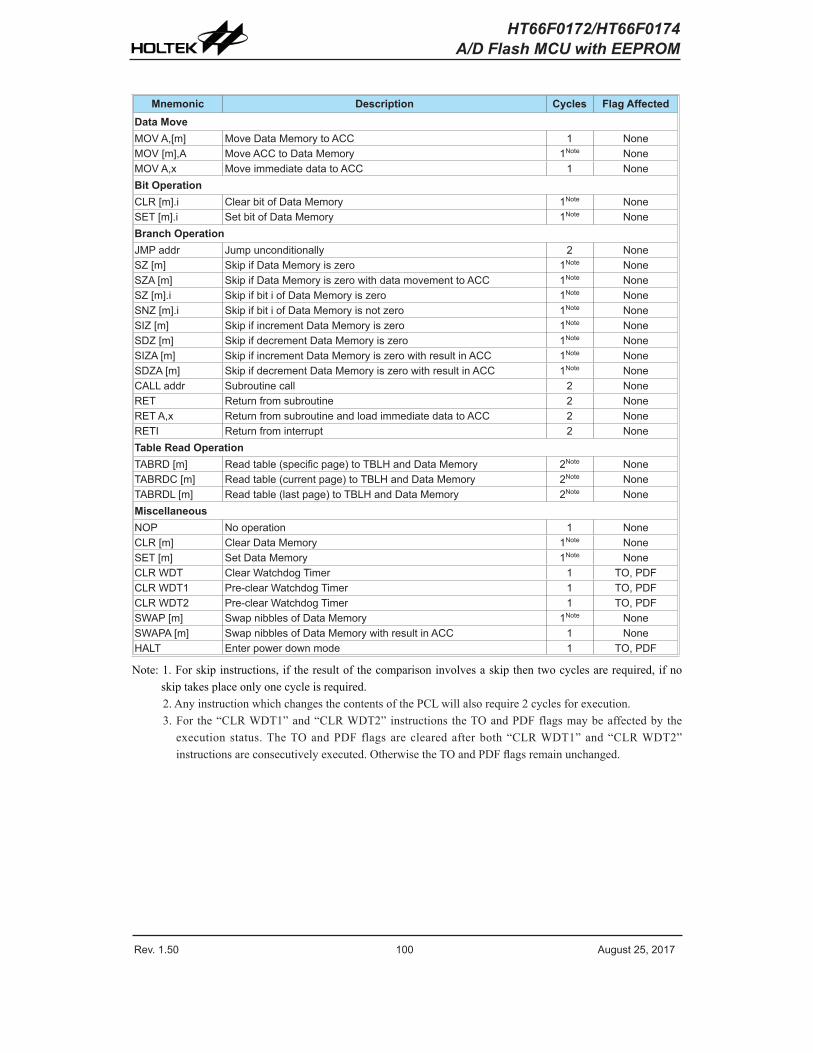
Rev. 1.50 100 ����st �5� �01� Rev. 1.50 101 ����st �5� �01�
HT66F0172/HT66F0174A/D Flash MCU with EEPROM
Mnemonic Description Cycles Flag AffectedData MoveMOV ��[m] Move Data Memory to �CC 1 NoneMOV [m]�� Move �CC to Data Memory 1Note NoneMOV ��x Move immediate data to �CC 1 NoneBit OperationCLR [m].i Clear bit of Data Memory 1Note NoneSET [m].i Set bit of Data Memory 1Note NoneBranch OperationJMP addr J�mp �nconditionally � NoneSZ [m] Skip if Data Memory is zero 1Note NoneSZ� [m] Skip if Data Memory is zero with data movement to �CC 1Note NoneSZ [m].i Skip if bit i of Data Memory is zero 1Note NoneSNZ [m].i Skip if bit i of Data Memory is not zero 1Note NoneSIZ [m] Skip if increment Data Memory is zero 1Note NoneSDZ [m] Skip if decrement Data Memory is zero 1Note NoneSIZ� [m] Skip if increment Data Memory is zero with res�lt in �CC 1Note NoneSDZ� [m] Skip if decrement Data Memory is zero with res�lt in �CC 1Note NoneC�LL addr S�bro�tine call � NoneRET Ret�rn from s�bro�tine � NoneRET ��x Ret�rn from s�bro�tine and load immediate data to �CC � NoneRETI Ret�rn from interr�pt � NoneTable Read OperationT�BRD [m] Read table (specific page) to TBLH and Data Memory �Note NoneT�BRDC [m] Read table (c�rrent pa�e) to TBLH and Data Memory �Note NoneT�BRDL [m] Read table (last pa�e) to TBLH and Data Memory �Note NoneMiscellaneousNOP No operation 1 NoneCLR [m] Clear Data Memory 1Note NoneSET [m] Set Data Memory 1Note NoneCLR WDT Clear Watchdo� Timer 1 TO� PDFCLR WDT1 Pre-clear Watchdo� Timer 1 TO� PDFCLR WDT� Pre-clear Watchdo� Timer 1 TO� PDFSW�P [m] Swap nibbles of Data Memory 1Note NoneSW�P� [m] Swap nibbles of Data Memory with res�lt in �CC 1 NoneH�LT Enter power down mode 1 TO� PDF
Note:1.Forskipinstructions,iftheresultofthecomparisoninvolvesaskipthentwocyclesarerequired,ifnoskiptakesplaceonlyonecycleisrequired.2.AnyinstructionwhichchangesthecontentsofthePCLwillalsorequire2cyclesforexecution.3.For the“CLRWDT1”and“CLRWDT2”instructionstheTOandPDFflagsmaybeaffectedbytheexecution status.TheTOandPDFflagsareclearedafterboth“CLRWDT1”and“CLRWDT2”instructionsareconsecutivelyexecuted.OtherwisetheTOandPDFflagsremainunchanged.

Rev. 1.50 100 ����st �5� �01� Rev. 1.50 101 ����st �5� �01�
HT66F0172/HT66F0174A/D Flash MCU with EEPROM
Instruction Definition
ADC A,[m] AddDataMemorytoACCwithCarryDescription ThecontentsofthespecifiedDataMemory,Accumulatorandthecarryflagareadded. TheresultisstoredintheAccumulator.Operation ACC←ACC+[m]+CAffectedflag(s) OV,Z,AC,C
ADCM A,[m] AddACCtoDataMemorywithCarryDescription ThecontentsofthespecifiedDataMemory,Accumulatorandthecarryflagareadded. TheresultisstoredinthespecifiedDataMemory.Operation [m]←ACC+[m]+CAffectedflag(s) OV,Z,AC,C
ADD A,[m] AddDataMemorytoACCDescription ThecontentsofthespecifiedDataMemoryandtheAccumulatorareadded. TheresultisstoredintheAccumulator.Operation ACC←ACC+[m]Affectedflag(s) OV,Z,AC,C
ADD A,x AddimmediatedatatoACCDescription ThecontentsoftheAccumulatorandthespecifiedimmediatedataareadded. TheresultisstoredintheAccumulator.Operation ACC←ACC+xAffectedflag(s) OV,Z,AC,C
ADDM A,[m] AddACCtoDataMemoryDescription ThecontentsofthespecifiedDataMemoryandtheAccumulatorareadded. TheresultisstoredinthespecifiedDataMemory.Operation [m]←ACC+[m]Affectedflag(s) OV,Z,AC,C
AND A,[m] LogicalANDDataMemorytoACCDescription DataintheAccumulatorandthespecifiedDataMemoryperformabitwiselogicalAND operation.TheresultisstoredintheAccumulator.Operation ACC←ACC″AND″[m]Affectedflag(s) Z
AND A,x LogicalANDimmediatedatatoACCDescription DataintheAccumulatorandthespecifiedimmediatedataperformabitwiselogicalAND operation.TheresultisstoredintheAccumulator.Operation ACC←ACC″AND″xAffectedflag(s) Z
ANDM A,[m] LogicalANDACCtoDataMemoryDescription DatainthespecifiedDataMemoryandtheAccumulatorperformabitwiselogicalAND operation.TheresultisstoredintheDataMemory.Operation [m]←ACC″AND″[m]Affectedflag(s) Z

Rev. 1.50 10� ����st �5� �01� Rev. 1.50 103 ����st �5� �01�
HT66F0172/HT66F0174A/D Flash MCU with EEPROM
CALL addr SubroutinecallDescription Unconditionallycallsasubroutineatthespecifiedaddress.TheProgramCounterthen incrementsby1toobtaintheaddressofthenextinstructionwhichisthenpushedontothe stack.Thespecifiedaddressisthenloadedandtheprogramcontinuesexecutionfromthis newaddress.Asthisinstructionrequiresanadditionaloperation,itisatwocycleinstruction.Operation Stack←ProgramCounter+1 ProgramCounter←addrAffectedflag(s) None
CLR [m] ClearDataMemoryDescription EachbitofthespecifiedDataMemoryisclearedto0.Operation [m]←00HAffectedflag(s) None
CLR [m].i ClearbitofDataMemoryDescription BitiofthespecifiedDataMemoryisclearedto0.Operation [m].i←0Affectedflag(s) None
CLR WDT ClearWatchdogTimerDescription TheTO,PDFflagsandtheWDTareallcleared.Operation WDTcleared TO←0 PDF←0Affectedflag(s) TO,PDF
CLR WDT1 Pre-clearWatchdogTimerDescription TheTO,PDFflagsandtheWDTareallcleared.Notethatthisinstructionworksin conjunctionwithCLRWDT2andmustbeexecutedalternatelywithCLRWDT2tohave effect.RepetitivelyexecutingthisinstructionwithoutalternatelyexecutingCLRWDT2will havenoeffect.Operation WDTcleared TO←0 PDF←0Affectedflag(s) TO,PDF
CLR WDT2 Pre-clearWatchdogTimerDescription TheTO,PDFflagsandtheWDTareallcleared.Notethatthisinstructionworksinconjunction withCLRWDT1andmustbeexecutedalternatelywithCLRWDT1tohaveeffect. RepetitivelyexecutingthisinstructionwithoutalternatelyexecutingCLRWDT1willhaveno effect.Operation WDTcleared TO←0 PDF←0Affectedflag(s) TO,PDF
CPL [m] ComplementDataMemoryDescription EachbitofthespecifiedDataMemoryislogicallycomplemented(1′scomplement).Bitswhich previouslycontaineda1arechangedto0andviceversa.Operation [m]←[m]Affectedflag(s) Z

Rev. 1.50 10� ����st �5� �01� Rev. 1.50 103 ����st �5� �01�
HT66F0172/HT66F0174A/D Flash MCU with EEPROM
CPLA [m] ComplementDataMemorywithresultinACCDescription EachbitofthespecifiedDataMemoryislogicallycomplemented(1′scomplement).Bitswhich previouslycontaineda1arechangedto0andviceversa.Thecomplementedresultisstoredin theAccumulatorandthecontentsoftheDataMemoryremainunchanged.Operation ACC←[m]Affectedflag(s) Z
DAA [m] Decimal-AdjustACCforadditionwithresultinDataMemoryDescription ConvertthecontentsoftheAccumulatorvaluetoaBCD(BinaryCodedDecimal)value resultingfromthepreviousadditionoftwoBCDvariables.Ifthelownibbleisgreaterthan9 orifACflagisset,thenavalueof6willbeaddedtothelownibble.Otherwisethelownibble remainsunchanged.Ifthehighnibbleisgreaterthan9oriftheCflagisset,thenavalueof6 willbeaddedtothehighnibble.Essentially,thedecimalconversionisperformedbyadding 00H,06H,60Hor66HdependingontheAccumulatorandflagconditions.OnlytheCflag maybeaffectedbythisinstructionwhichindicatesthatiftheoriginalBCDsumisgreaterthan 100,itallowsmultipleprecisiondecimaladdition.Operation [m]←ACC+00Hor [m]←ACC+06Hor [m]←ACC+60Hor [m]←ACC+66HAffectedflag(s) C
DEC [m] DecrementDataMemoryDescription DatainthespecifiedDataMemoryisdecrementedby1.Operation [m]←[m]−1Affectedflag(s) Z
DECA [m] DecrementDataMemorywithresultinACCDescription DatainthespecifiedDataMemoryisdecrementedby1.Theresultisstoredinthe Accumulator.ThecontentsoftheDataMemoryremainunchanged.Operation ACC←[m]−1Affectedflag(s) Z
HALT EnterpowerdownmodeDescription Thisinstructionstopstheprogramexecutionandturnsoffthesystemclock.Thecontentsof theDataMemoryandregistersareretained.TheWDTandprescalerarecleared.Thepower downflagPDFissetandtheWDTtime-outflagTOiscleared.Operation TO←0 PDF←1Affectedflag(s) TO,PDF
INC [m] IncrementDataMemoryDescription DatainthespecifiedDataMemoryisincrementedby1.Operation [m]←[m]+1Affectedflag(s) Z
INCA [m] IncrementDataMemorywithresultinACCDescription DatainthespecifiedDataMemoryisincrementedby1.TheresultisstoredintheAccumulator. ThecontentsoftheDataMemoryremainunchanged.Operation ACC←[m]+1Affectedflag(s) Z

Rev. 1.50 104 ����st �5� �01� Rev. 1.50 105 ����st �5� �01�
HT66F0172/HT66F0174A/D Flash MCU with EEPROM
JMP addr JumpunconditionallyDescription ThecontentsoftheProgramCounterarereplacedwiththespecifiedaddress.Program executionthencontinuesfromthisnewaddress.Asthisrequirestheinsertionofadummy instructionwhilethenewaddressisloaded,itisatwocycleinstruction.Operation ProgramCounter←addrAffectedflag(s) None
MOV A,[m] MoveDataMemorytoACCDescription ThecontentsofthespecifiedDataMemoryarecopiedtotheAccumulator.Operation ACC←[m]Affectedflag(s) None
MOV A,x MoveimmediatedatatoACCDescription TheimmediatedataspecifiedisloadedintotheAccumulator.Operation ACC←xAffectedflag(s) None
MOV [m],A MoveACCtoDataMemoryDescription ThecontentsoftheAccumulatorarecopiedtothespecifiedDataMemory.Operation [m]←ACCAffectedflag(s) None
NOP NooperationDescription Nooperationisperformed.Executioncontinueswiththenextinstruction.Operation NooperationAffectedflag(s) None
OR A,[m] LogicalORDataMemorytoACCDescription DataintheAccumulatorandthespecifiedDataMemoryperformabitwise logicalORoperation.TheresultisstoredintheAccumulator.Operation ACC←ACC″OR″[m]Affectedflag(s) Z
OR A,x LogicalORimmediatedatatoACCDescription DataintheAccumulatorandthespecifiedimmediatedataperformabitwiselogicalOR operation.TheresultisstoredintheAccumulator.Operation ACC←ACC″OR″xAffectedflag(s) Z
ORM A,[m] LogicalORACCtoDataMemoryDescription DatainthespecifiedDataMemoryandtheAccumulatorperformabitwiselogicalOR operation.TheresultisstoredintheDataMemory.Operation [m]←ACC″OR″[m]Affectedflag(s) Z
RET ReturnfromsubroutineDescription TheProgramCounterisrestoredfromthestack.Programexecutioncontinuesattherestored address.Operation ProgramCounter←StackAffectedflag(s) None

Rev. 1.50 104 ����st �5� �01� Rev. 1.50 105 ����st �5� �01�
HT66F0172/HT66F0174A/D Flash MCU with EEPROM
RET A,x ReturnfromsubroutineandloadimmediatedatatoACCDescription TheProgramCounterisrestoredfromthestackandtheAccumulatorloadedwiththespecified immediatedata.Programexecutioncontinuesattherestoredaddress.Operation ProgramCounter←Stack ACC←xAffectedflag(s) None
RETI ReturnfrominterruptDescription TheProgramCounterisrestoredfromthestackandtheinterruptsarere-enabledbysettingthe EMIbit.EMIisthemasterinterruptglobalenablebit.Ifaninterruptwaspendingwhenthe RETIinstructionisexecuted,thependingInterruptroutinewillbeprocessedbeforereturning tothemainprogram.Operation ProgramCounter←Stack EMI←1Affectedflag(s) None
RL [m] RotateDataMemoryleftDescription ThecontentsofthespecifiedDataMemoryarerotatedleftby1bitwithbit7rotatedintobit0.Operation [m].(i+1)←[m].i;(i=0~6) [m].0←[m].7Affectedflag(s) None
RLA [m] RotateDataMemoryleftwithresultinACCDescription ThecontentsofthespecifiedDataMemoryarerotatedleftby1bitwithbit7rotatedintobit0. TherotatedresultisstoredintheAccumulatorandthecontentsoftheDataMemoryremain unchanged.Operation ACC.(i+1)←[m].i;(i=0~6) ACC.0←[m].7Affectedflag(s) None
RLC [m] RotateDataMemoryleftthroughCarryDescription ThecontentsofthespecifiedDataMemoryandthecarryflagarerotatedleftby1bit.Bit7 replacestheCarrybitandtheoriginalcarryflagisrotatedintobit0.Operation [m].(i+1)←[m].i;(i=0~6) [m].0←C C←[m].7Affectedflag(s) C
RLCA [m] RotateDataMemoryleftthroughCarrywithresultinACCDescription DatainthespecifiedDataMemoryandthecarryflagarerotatedleftby1bit.Bit7replacesthe Carrybitandtheoriginalcarryflagisrotatedintothebit0.Therotatedresultisstoredinthe AccumulatorandthecontentsoftheDataMemoryremainunchanged.Operation ACC.(i+1)←[m].i;(i=0~6) ACC.0←C C←[m].7Affectedflag(s) C
RR [m] RotateDataMemoryrightDescription ThecontentsofthespecifiedDataMemoryarerotatedrightby1bitwithbit0rotatedintobit7.Operation [m].i←[m].(i+1);(i=0~6) [m].7←[m].0Affectedflag(s) None

Rev. 1.50 106 ����st �5� �01� Rev. 1.50 10� ����st �5� �01�
HT66F0172/HT66F0174A/D Flash MCU with EEPROM
RRA [m] RotateDataMemoryrightwithresultinACCDescription DatainthespecifiedDataMemoryandthecarryflagarerotatedrightby1bitwithbit0 rotatedintobit7.TherotatedresultisstoredintheAccumulatorandthecontentsofthe DataMemoryremainunchanged.Operation ACC.i←[m].(i+1);(i=0~6) ACC.7←[m].0Affectedflag(s) None
RRC [m] RotateDataMemoryrightthroughCarryDescription ThecontentsofthespecifiedDataMemoryandthecarryflagarerotatedrightby1bit.Bit0 replacestheCarrybitandtheoriginalcarryflagisrotatedintobit7.Operation [m].i←[m].(i+1);(i=0~6) [m].7←C C←[m].0Affectedflag(s) C
RRCA [m] RotateDataMemoryrightthroughCarrywithresultinACCDescription DatainthespecifiedDataMemoryandthecarryflagarerotatedrightby1bit.Bit0replaces theCarrybitandtheoriginalcarryflagisrotatedintobit7.Therotatedresultisstoredinthe AccumulatorandthecontentsoftheDataMemoryremainunchanged.Operation ACC.i←[m].(i+1);(i=0~6) ACC.7←C C←[m].0Affectedflag(s) C
SBC A,[m] SubtractDataMemoryfromACCwithCarryDescription ThecontentsofthespecifiedDataMemoryandthecomplementofthecarryflagare subtractedfromtheAccumulator.TheresultisstoredintheAccumulator.Notethatifthe resultofsubtractionisnegative,theCflagwillbeclearedto0,otherwiseiftheresultis positiveorzero,theCflagwillbesetto1.Operation ACC←ACC−[m]−CAffectedflag(s) OV,Z,AC,C
SBCM A,[m] SubtractDataMemoryfromACCwithCarryandresultinDataMemoryDescription ThecontentsofthespecifiedDataMemoryandthecomplementofthecarryflagare subtractedfromtheAccumulator.TheresultisstoredintheDataMemory.Notethatifthe resultofsubtractionisnegative,theCflagwillbeclearedto0,otherwiseiftheresultis positiveorzero,theCflagwillbesetto1.Operation [m]←ACC−[m]−CAffectedflag(s) OV,Z,AC,C
SDZ [m] SkipifdecrementDataMemoryis0Description ThecontentsofthespecifiedDataMemoryarefirstdecrementedby1.Iftheresultis0the followinginstructionisskipped.Asthisrequirestheinsertionofadummyinstructionwhile thenextinstructionisfetched,itisatwocycleinstruction.Iftheresultisnot0theprogram proceedswiththefollowinginstruction.Operation [m]←[m]−1 Skipif[m]=0Affectedflag(s) None
Rev. 1.50 106 ����st �5� �01� Rev. 1.50 10� ����st �5� �01�
HT66F0172/HT66F0174A/D Flash MCU with EEPROM
SDZA [m] SkipifdecrementDataMemoryiszerowithresultinACCDescription ThecontentsofthespecifiedDataMemoryarefirstdecrementedby1.Iftheresultis0,the followinginstructionisskipped.TheresultisstoredintheAccumulatorbutthespecified DataMemorycontentsremainunchanged.Asthisrequirestheinsertionofadummy instructionwhilethenextinstructionisfetched,itisatwocycleinstruction.Iftheresultisnot0, theprogramproceedswiththefollowinginstruction.Operation ACC←[m]−1 SkipifACC=0Affectedflag(s) None
SET [m] SetDataMemoryDescription EachbitofthespecifiedDataMemoryissetto1.Operation [m]←FFHAffectedflag(s) None
SET [m].i SetbitofDataMemoryDescription BitiofthespecifiedDataMemoryissetto1.Operation [m].i←1Affectedflag(s) None
SIZ [m] SkipifincrementDataMemoryis0Description ThecontentsofthespecifiedDataMemoryarefirstincrementedby1.Iftheresultis0,the followinginstructionisskipped.Asthisrequirestheinsertionofadummyinstructionwhile thenextinstructionisfetched,itisatwocycleinstruction.Iftheresultisnot0theprogram proceedswiththefollowinginstruction.Operation [m]←[m]+1 Skipif[m]=0Affectedflag(s) None
SIZA [m] SkipifincrementDataMemoryiszerowithresultinACCDescription ThecontentsofthespecifiedDataMemoryarefirstincrementedby1.Iftheresultis0,the followinginstructionisskipped.TheresultisstoredintheAccumulatorbutthespecified DataMemorycontentsremainunchanged.Asthisrequirestheinsertionofadummy instructionwhilethenextinstructionisfetched,itisatwocycleinstruction.Iftheresultisnot 0theprogramproceedswiththefollowinginstruction.Operation ACC←[m]+1 SkipifACC=0Affectedflag(s) None
SNZ [m].i SkipifbitiofDataMemoryisnot0Description IfbitiofthespecifiedDataMemoryisnot0,thefollowinginstructionisskipped.Asthis requirestheinsertionofadummyinstructionwhilethenextinstructionisfetched,itisatwo cycleinstruction.Iftheresultis0theprogramproceedswiththefollowinginstruction.Operation Skipif[m].i≠0Affectedflag(s) None
SUB A,[m] SubtractDataMemoryfromACCDescription ThespecifiedDataMemoryissubtractedfromthecontentsoftheAccumulator.Theresultis storedintheAccumulator.Notethatiftheresultofsubtractionisnegative,theCflagwillbe clearedto0,otherwiseiftheresultispositiveorzero,theCflagwillbesetto1.Operation ACC←ACC−[m]Affectedflag(s) OV,Z,AC,C

Rev. 1.50 108 ����st �5� �01� Rev. 1.50 109 ����st �5� �01�
HT66F0172/HT66F0174A/D Flash MCU with EEPROM
SUBM A,[m] SubtractDataMemoryfromACCwithresultinDataMemoryDescription ThespecifiedDataMemoryissubtractedfromthecontentsoftheAccumulator.Theresultis storedintheDataMemory.Notethatiftheresultofsubtractionisnegative,theCflagwillbe clearedto0,otherwiseiftheresultispositiveorzero,theCflagwillbesetto1.Operation [m]←ACC−[m]Affectedflag(s) OV,Z,AC,C
SUB A,x SubtractimmediatedatafromACCDescription TheimmediatedataspecifiedbythecodeissubtractedfromthecontentsoftheAccumulator. TheresultisstoredintheAccumulator.Notethatiftheresultofsubtractionisnegative,theC flagwillbeclearedto0,otherwiseiftheresultispositiveorzero,theCflagwillbesetto1.Operation ACC←ACC−xAffectedflag(s) OV,Z,AC,C
SWAP [m] SwapnibblesofDataMemoryDescription Thelow-orderandhigh-ordernibblesofthespecifiedDataMemoryareinterchanged.Operation [m].3~[m].0↔[m].7~[m].4Affectedflag(s) None
SWAPA [m] SwapnibblesofDataMemorywithresultinACCDescription Thelow-orderandhigh-ordernibblesofthespecifiedDataMemoryareinterchanged.The resultisstoredintheAccumulator.ThecontentsoftheDataMemoryremainunchanged.Operation ACC.3~ACC.0←[m].7~[m].4 ACC.7~ACC.4←[m].3~[m].0Affectedflag(s) None
SZ [m] SkipifDataMemoryis0Description IfthecontentsofthespecifiedDataMemoryis0,thefollowinginstructionisskipped.Asthis requirestheinsertionofadummyinstructionwhilethenextinstructionisfetched,itisatwo cycleinstruction.Iftheresultisnot0theprogramproceedswiththefollowinginstruction.Operation Skipif[m]=0Affectedflag(s) None
SZA [m] SkipifDataMemoryis0withdatamovementtoACCDescription ThecontentsofthespecifiedDataMemoryarecopiedtotheAccumulator.Ifthevalueiszero, thefollowinginstructionisskipped.Asthisrequirestheinsertionofadummyinstruction whilethenextinstructionisfetched,itisatwocycleinstruction.Iftheresultisnot0the programproceedswiththefollowinginstruction.Operation ACC←[m] Skipif[m]=0Affectedflag(s) None
SZ [m].i SkipifbitiofDataMemoryis0Description IfbitiofthespecifiedDataMemoryis0,thefollowinginstructionisskipped.Asthisrequires theinsertionofadummyinstructionwhilethenextinstructionisfetched,itisatwocycle instruction.Iftheresultisnot0,theprogramproceedswiththefollowinginstruction.Operation Skipif[m].i=0Affectedflag(s) None

Rev. 1.50 108 ����st �5� �01� Rev. 1.50 109 ����st �5� �01�
HT66F0172/HT66F0174A/D Flash MCU with EEPROM
TABRD [m] Readtable(specificpage)toTBLHandDataMemoryDescription Thelowbyteoftheprogramcode(specificpage)addressedbythetablepointerpair (TBHPandTBLP)ismovedtothespecifiedDataMemoryandthehighbytemovedtoTBLH.Operation [m]←programcode(lowbyte) TBLH←programcode(highbyte)Affectedflag(s) None
TABRDC [m] Readtable(currentpage)toTBLHandDataMemoryDescription Thelowbyteoftheprogramcode(currentpage)addressedbythetablepointer(TBLP)is movedtothespecifiedDataMemoryandthehighbytemovedtoTBLH.Operation [m]←programcode(lowbyte) TBLH←programcode(highbyte)Affectedflag(s) None
TABRDL [m] Readtable(lastpage)toTBLHandDataMemoryDescription Thelowbyteoftheprogramcode(lastpage)addressedbythetablepointer(TBLP)ismoved tothespecifiedDataMemoryandthehighbytemovedtoTBLH.Operation [m]←programcode(lowbyte) TBLH←programcode(highbyte)Affectedflag(s) None
XOR A,[m] LogicalXORDataMemorytoACCDescription DataintheAccumulatorandthespecifiedDataMemoryperformabitwiselogicalXOR operation.TheresultisstoredintheAccumulator.Operation ACC←ACC″XOR″[m]Affectedflag(s) Z
XORM A,[m] LogicalXORACCtoDataMemoryDescription DatainthespecifiedDataMemoryandtheAccumulatorperformabitwiselogicalXOR operation.TheresultisstoredintheDataMemory.Operation [m]←ACC″XOR″[m]Affectedflag(s) Z
XOR A,x LogicalXORimmediatedatatoACCDescription DataintheAccumulatorandthespecifiedimmediatedataperformabitwiselogicalXOR operation.TheresultisstoredintheAccumulator.Operation ACC←ACC″XOR″xAffectedflag(s) Z

Rev. 1.50 110 ����st �5� �01� Rev. 1.50 111 ����st �5� �01�
HT66F0172/HT66F0174A/D Flash MCU with EEPROM
Package Information
Note that thepackage informationprovidedhere is for consultationpurposesonly.As thisinformationmaybeupdatedatregularintervalsusersareremindedtoconsulttheHoltekwebsiteforthelatestversionofthePackage/CartonInformation.
Additionalsupplementaryinformationwithregardtopackagingislistedbelow.Clickontherelevantsectiontobetransferredtotherelevantwebsitepage.
• FurtherPackageInformation(includeOutlineDimensions,ProductTapeandReelSpecifications)
• PackingMeterialsInformation
• Cartoninformation

Rev. 1.50 110 ����st �5� �01� Rev. 1.50 111 ����st �5� �01�
HT66F0172/HT66F0174A/D Flash MCU with EEPROM
20-pin SOP (300mil) Outline Dimensions
� �
�
� �
� �
� �
�
�
� �
� ��
�
�
SymbolDimensions in inch
Min. Nom. Max.� — 0.406 BSC —B — 0.�95 BSC —C 0.01� — 0.0�0 C’ — 0.504 BSC —D — — 0.104 E — 0.050 BSC —F 0.004 — 0.01� G 0.016 — 0.050 H 0.008 — 0.013 α 0° — 8°
SymbolDimensions in mm
Min. Nom. Max.� — 10.30 BSC —B — �.50 BSC —C 0.31 — 0.51 C’ — 1�.80 BSC —D — — �.65 E — 1.�� BSC —F 0.10 — 0.30 G 0.40 — 1.�� H 0.�0 — 0.33 α 0° — 8°
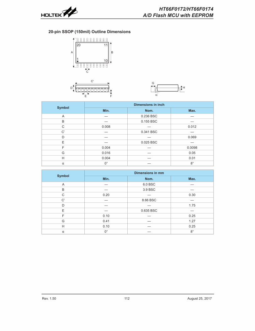
Rev. 1.50 11� ����st �5� �01� Rev. 1.50 113 ����st �5� �01�
HT66F0172/HT66F0174A/D Flash MCU with EEPROM
20-pin SSOP (150mil) Outline Dimensions
� �
�
� �
� �
� �
�
�
� �
� � ��
�
SymbolDimensions in inch
Min. Nom. Max.� — 0.�36 BSC —B — 0.155 BSC —C 0.008 — 0.01� C’ — 0.341 BSC —D — — 0.069 E — 0.0�5 BSC —F 0.004 — 0.0098 G 0.016 — 0.05 H 0.004 — 0.01 α 0° — 8°
SymbolDimensions in mm
Min. Nom. Max.� — 6.0 BSC —B — 3.9 BSC —C 0.�0 — 0.30 C’ — 8.66 BSC —D — — 1.�5 E — 0.635 BSC —F 0.10 — 0.�5 G 0.41 — 1.�� H 0.10 — 0.�5 α 0° — 8°

Rev. 1.50 11� ����st �5� �01� Rev. 1.50 113 ����st �5� �01�
HT66F0172/HT66F0174A/D Flash MCU with EEPROM
Copyri�ht© �01� by HOLTEK SEMICONDUCTOR INC.
The information appearin� in this Data Sheet is believed to be acc�rate at the time of p�blication. However� Holtek ass�mes no responsibility arisin� from the �se of the specifications described. The applications mentioned herein are used solely for the p�rpose of ill�stration and Holtek makes no warranty or representation that s�ch applications will be s�itable witho�t f�rther modification� nor recommends the �se of its prod�cts for application that may present a risk to h�man life d�e to malf�nction or otherwise. Holtek's prod�cts are not a�thorized for �se as critical components in life s�pport devices or systems. Holtek reserves the ri�ht to alter its products without prior notification. For the most up-to-date information, please visit o�r web site at http://www.holtek.com.tw.