achievements and results annual report 2002 · 2020-04-27 · warfare agents. • assembly and...
TRANSCRIPT

Achievements and ResultsAnnual Report 2002

Modern work places atFraunhofer ISIT: employee in the cleanroom environment.

Achievements and ResultsAnnual Report 2002

Preface............................................. 6
Profile of the InstituteBrief Portrait .................................... 12
Main Fields of Activity ...................... 14
Offers for Research and ServiceService Offers .................................. 24
Customers ....................................... 26
Innovation Catalogue ...................... 28
Representative Figures ................. 30
The Fraunhofer-Gesellschaft at a Glance ..................................... 32
Representative Results of Work
IC-TechnologySuper Junction Devices for High Voltage PowerMOS ................. 34
Passive Components: High Precision Chip-Capacitors forGHz-Application Passive ................... 36
Patterning of Magnetic Hard Disks with Ion-Projection ......... 38
Microsystems TechnologyStudy on Bistable Thermomechanical Drives ................ 40
Glass Flow Process GFP -A Novel Micromachining Technology for Structuring Borosilicate Glass Substrates ............ 42
Silicon Etching of Deep Trenches with High Aspect Ratio .................... 44
Access to Microsystem Production - Co-operation within EUROPRACTICE .................... 45
IC-DesignDesign-Kit for Microsystem Designers ..................... 46
Biotechnical MicrosystemsElectrical Manipulation of DNA Molecules ................................ 48
Portable Monitoring Systems forProtein Detection ............................. 50
Module IntegrationLow-Profile and Flexible Electronic Assemblies Using Ultra-Thin Silicon ............................. 52
Business Opportunities for Advanced Packaging in Europe ........ 57
Integrated Power SystemsHearing-Aids with Rechargeable Power Supply (HARPOS) .................. 60
Important Names, Data, Events
Lecturing Assignments at Universities .................................. 64
Memberships in Coordinationboardsand Committees ............................... 64
Cooperation with Institutes andUniversities ...................................... 64
Trade Fairs and Exhibitions ............... 65
Miscellaneous Events ....................... 65
Scientific PublicationsJournal Papers and Contributions to Conferences .......... 66
Talks and Poster Presentations ..........66
Doctoral Theses ............................. 68
Diploma Theses ............................. 68
Patents ........................................... 68
General View on Projects ............. 69
Contact and Further Information ................................... 71
Imprint ........................................... 71
Achievements and Results Annual Report 2002

6 Fraunhofer ISIT Achievements and Results – Annual Report 2002
Fraunhofer ISIT, a chrystalisation point for differentcompanies in Itzehoe: (from front to rear: Prokon,IZET, Fraunhofer ISIT, SMI, Solid Energy and Condias.
New production hall for SolidEnergy and Condias.
New spin-off companies in Itzehoe play a majorrole in this context, in cases where it has beencontractually agreed that a large part of theirproduct development work will take place incooperation with ISIT.
In 2002 important landmarks were achieved forISIT and the high-technology location ofItzehoe. During the summer a new productionhall for the companies Solid Energy andCondias in the direct vicinity of the FraunhoferISIT was completed and officially opened byeconomics minister Dr. Bernd Rohwer and member of parliament Dietrich Austermann.
The new building complex includes a productionhall of 1,875 square meters and a connectedtwo-story administration wing providing600 square meters of office space. The cost of the building totalled 1.8 millioneuros. A further 5.4 million euros was investedin additional hall infrastructure and productionfacilities, of which 3.7 million euros were raisedby Solid Energy and 1.8 million euros byCondias. In the medium term these companieswill together create 75 jobs.
Both firms are without doubt among the biggest and technically most advanced newspin-off companies of the Fraunhofer-Gesell-
schaft in recent years. Condias, which was established by the Fraunhofer Institute forSurface Engineering and Thin Films,Braunschweig, has installed a production unitfor the manufacture of conductive diamond coatings in the new hall, from where it suppliesits customers. These diamond coatings find usein a wide range of applications, such as in theenvironmental sector, where they are employedin the ecologically beneficial processing of substances that are otherwise difficult to dispose of safely. Solid Energy, a business spin-off from the ISIT, intends to build a production line in the hall to make lithium batteries for the telecommunications market.
Solid Energy is highly regarded in the state ofSchleswig-Holstein as an example of successfultechnology transfer. In November the companywas presented with the Schmidt-RömhildTechnology Award 2002 by economics ministerDr. Bernd Rohwer. This award was inauguratedby Lübeck-based publishing house Schmidt-Römhild to honor pioneering developments bysmall firms in Schleswig-Holstein.
But the opening of the new production hall wasnot the only event to generate optimism, and itwas also good to see the resumption of buil-ding work at the neighboring firm SMI GmbH.
Preface
8 Fraunhofer ISIT Achievements and Results – Annual Report 2002
The construction of a new silicon chip factoryhad been halted in spring 2001 owing to thegeneral recession in the semiconductor industry.Now the management of Philips has decided to resume the planned activities. As a first stepthe development and administration building is being completed. The work is now almostfinished.
Naturally, an applied research institute such as ISIT can only occupy a firm long-term position in the market if it is able to produce asteady stream of innovative ideas and tech-
Fraunhofer ISIT Achievements and Results – Annual Report 2002 9
Impressions of the opening of the new factory building forSolid Energy and Condias right next to the Fraunhofer ISITon June 24, 2002.Founded Condias: Dr. Matthias Fryda, Dr. Thorsten Matthée;ISIT-curator Dietrich Austermann;take care for music: Iris Kramer and Hròlfur Vagnsson.
Be glad about two new companies in Itzehoe: Dr. Ingo Hussla head of IZET, Condias founder Dr. Matthias Fryda and Dr. Thorsten Matthée, mayor ofItzehoe Harald Brommer, ISIT-curator and member of parliament Dietrich Austermann, minister of economic affairs in Schleswig-Holstein Dr. Bernd Rohwer, Prof. Anton Heuberger head of ISIT and Solid Energy founder Dr. Gerold Neumann.

10 Fraunhofer ISIT Achievements and Results – Annual Report 2002
nologies. Without this capability the appealing technological concept of ISIT, based on its close links to production, would be ineffective.Adequate application-oriented basic research is therefore required which covers a time-frame of between five and ten years. The result of this advance research must, however, be to create products as quickly aspossible and to transfer them to industrial use.In the absence of such a strategy, advance research can become indistinct from basic research of no entrepreneurial value. The major subject areas of long-term advanceresearch currently pursued by ISIT are as follows:
• Power electronics: New integration techniques for power components used in mains-operated applications with a blocking ability of up to
Preface
1
IC-Technology
FriedrichDr. Zwicker
SecretaryGreiff, Rosemann,
Wiegandt
MANAGEMENT
Managing DirectorProf. Dr. Heuberger
Member of Institute ManagementDr. Windbracke
Design / SimulationEichholz
2
MicrosystemTechnology
Dr. WagnerDr. Reimer
Administration
Finder
TASKS
Planning of R&D areas in co-operation with Universities: Dr. Bernt
Marketing: Dr. DuddePublic Relations: Wacker
Building and Installation: Dr. KrullmannQuality Management: Dr. Petzold
4
Packaging,Module
Integration
Pape
3
BiotechnicalSystems
Dr. Hintsche
ISIT Organigram
5
IntegratedPower Systems
Dr. Gulde
1200 V. The aim here is to develop monoli-thic integration techniques in silicon in orderto supply the foreseeable high-volume new markets with miniaturized components atacceptable cost.
• Microsystem technology: Development of improved surface micromechanics which can be integratedwith CMOS, mainly with the objective of realizing the next generations of mirror arrays(for example, large array fields with1,000 positions for fiber-optic technology, or more-robust mirror systems for use in portable systems, such as GPS in mobile phones).
• Biosensor systems: Development of a wafer-scale biocoating technology on thebasis of inkjet printing for the manufactureof application-specific biosensors. The application goals pursued by ISIT,

together with its spin-off firm eBiochipSystems GmbH, focus on special subjects inmedical engineering, food monitoring andthe development of measuring systems for the continuous detection biological warfare agents.
• Assembly and interconnection technology:Further development of wafer-scale packaging techniques incorporating 'balling'technologies, serving as the basis to set up a service company in this field in Itzehoe.The main aim here is to make a contribution towards the successful return of advanced AVT techniques from the FarEast to Europe.
• Lithium batteries: Development of lithium-polymer cells which are specially optimized for traction applications (42 V on-board supply system and hybrid drives). The basis for this is the development
and deployment of new coating systemsincorporating lithium-manganese-oxide spinels.
This summarizes an ambitious R&D programwhich, if successful, will without doubt attractconsiderable demand form industry.
Apart from the perpetual issues of financing,the quality of staff and their ability to contribu-te innovative ideas is of decisive importance. That ISIT and its staff possess this ability isimpressively confirmed by the work conductedup until today by the Institute. I would like to take the opportunity at this point to thank allstaff for their commitment and sunstantial efforts.
Fraunhofer ISIT Achievements and Results – Annual Report 2002 11
Anton Heuberger
Prof. Anton Heuberger, Dietrich Austermann (from left).
Solid Energy GmbH was honoured with the Schmidt-Römhild TechnologyAward 2002.
Dr. Gerold Neumann, mangagingdirector of Solid Energy.


Fraunhofer ISIT Achievements and Results – Annual Report 2002 13
The Fraunhofer-Institut für Siliziumtechnologie(ISIT), Itzehoe, works on design, developmentand production of microelectronic componentsas well as on microsensors, microactuators andother components for microsystems technology.All devices of this kind can be delivered eitherbeing prototypes or customer specific series.
Among the Fraunhofer institutes working onmicroelectronics ISIT is concentrating upon thedevelopment of new process technologies forsemiconductor silicon based components andmicrosystems.
In cooperation with the adjacent Innovations-zentrum (IZET) ISIT also aims at creating new jobswithin the high-tech field.
The institute is running a professional semicon-ductor production line together with the companyVishay Semiconductor Itzehoe GmbH. This line isused for the production of microelectronic devices(PowerMOS) and microsystems by Vishay as wellas for R&D projects for new components andtechnological processes by ISIT.
In view of its current and future production anddevelopment activities, especially for automotiveindustries, ISIT is establishing a quality manage-ment system which is going to be ISO 9001 certified in spring 2003.
Further services offered by the institute are theanalysis and development of technology pertai-ning to the quality and reliability of electronicassemblies as well as packaging and mountingtechnology for microsystems, sensors and multichip modules. A focal point of work in thisfield involves new packaging techniques forlarge-area microsystems.
A new activity is the development of advancedpower-supply components for electronic systems.
The complete institute staff consists of about150 employees.
Brief Portrait
Chemical-mechanical polishing (CMP),a process step for microelectronic andmicrosystem applications.

14 Fraunhofer ISIT Achievements and Results – Annual Report 2002
RF chip capacitors with solder bump termination, in size 500 µm by 1000 µm.

IC-Technology
The IC-Technology department is focused on the development and fabrication of active andpassive silicon based devices.
In the field of active devices IGBTs, PowerMOSand diodes are of special importance. Here, ISIT can rely on a qualified core technology forpower devices provided by our industrial partner.Customer specific development of power devices is supported by simulation, design andelectrical characterisation.
Further, ISIT has many years of experience indeveloping advanced CMOS processes with appropriate simulation and circuit design capability.
Passive components like chip-capacitors, -resistors and -coils are another field of ISIT activities. Evaluation of new materials and itsintegration in complete processes is one important topic for passive IC develpoment.
In addition ISIT offers customer specific waferprocessing in small and medium quantities basedon standard IC and MST technology. This includes the development of new single processes and process modules for all relevantfields of semiconductor technology.
Chemical-Mechanical Polishing
Planarisation by means of chemical-mechanicalpolishing (CMP) is a key process for the fabrication of advanced ICs. The institute’s CMPapplication lab is equipped with CMP clustertools, single- and double-sided polishers andpost-CMP cleaners for substrate diameters of upto 300 mm and offers services on all aspects ofCMP development like
• Testing of CMP equipment• Development of CMP processes for
- dielectrics (oxide, low-k materials, ...)- metals (tungsten, copper, ...)- silicon
• Testing of polishing slurries and pads• Post-CMP cleaning• CMP-related measurement• Custom-specific CMP services for device
manufacturing
In the field of CMP ISIT co-operates closely with equipment and pad/slurry manufacturers,production CMP users and the wafer industry.
Dr. Gerfried Zwicker+ 49 (0) 48 21 / 17-43 [email protected]
Main fields of Activity
Fraunhofer ISIT Achievements and Results – Annual Report 2002 15
Test structures for the development of new CMP processes.
Wet chemistry section.

Main fields of Activity
16 Fraunhofer ISIT Achievements and Results – Annual Report 2002
IC-Design
Besides the main tasks of designing and testingmixed-signal ASICs, mainly in co-operation within-house departments for microsystem develop-ment, the IC-Design department offers thedesign of micromechanical and microoptical elements using analogue HDL for modelling andIC-layout and IC-verification tools.
State of the art IC-Design, FEM and mathematicssoftware is used. For test purposes laboratoriesequipped with hardware for electrical measure-ments in time and frequency domain and formechanical and optical standard tests are available.
Over the years a number of helpful designtoolshave been developed to accelerate the design-flow from the idea to masklayout. Those toolsare part of special MEMS-design-kits to supportthe designer using micromechanical processes,including features like DRC, HDLA-models, cross-section viewer, layout generators and easy-to-handle user interfaces to mechanicalsimulators.
Jörg Eichholz+ 49 (0) 48 21 / 17 - 45 [email protected]
MEMS wafer on RF probe station.

Microsystems – MEMS
The MEMS department focuses on the appli-cation specific development of physical, optical,fluidic, and RF-MEMS components and the integration to microsystems. We have access tothe 6-inch silicon frontend technology of the in-house industrial semiconductor production. In addition, qualified MEMS processes are offeredin a foundry service, e.g. wet etching and deepRIE of silicon, thick resist lithography, grey-scalelithography, electroplating, epitaxial polysilicon,SOI-micromachining, glass micromachining, replication technologies, wafer bonding and chemical-mechanical polishing. In the EURO-PRACTICE frame we provide design-house servicealso for external MEMS foundry processes. The MEMS department works in close collabo-ration with the ASIC-Design and the packagingdepartments in order to offer integrated micro-system solutions.
The physical sensor work focuses mainly on auto-motive applications, especially sensors for angularrate, acceleration, pressure and air flow. Theoptical MEMS activities are driven by applicationsfor optical communication and measuring sys-tems. Examples are fiber-optic switching systems,laser scanners, digital micromirror arrays, spectro-meters, and also passive optical components, e.g.refractive and diffractive microlenses. RF-MEMScomponents, such as RF-switches, tunable capa-citors and micro-relays are developed for wirelesscommunication applications. Examples of fluidicmicrosystems are pneumatic microvalves, sensor-controlled micro-pipettes and micropumps.
Dr. Bernd Wagner+ 49 (0) 48 21 / 17 - 42 [email protected]
Dr. Klaus Reimer+ 49 (0) 48 21 / 17 - 45 [email protected]
Fraunhofer ISIT Achievements and Results – Annual Report 2002 17
Automated sensor controlled micro pipetting system formicro titer plates.

Biotechnical Microsystems
The department Biotechnical Microsystems isfocusing its activities in the field of electrical biosensor technologies. Our activities aim at thedesign and construction of novel sensing arraysin miniaturized formats. The development ofultramicroelectrodes arrays enable novel bio-sensor constructions and the evaluation of highlysensitive and new approaches of selective detecting principles, e.g. the redox recycling ofELISA based assay products and impedance spectroscopy.
The integration of the transducers made in silicon technology and microfluidic systems withelectrical manipulation of biomolecules opensnew applications in biochemical assays, medicaldiagnostics and environmental analytics.
Sub-µm-electrode arrays have been developed asthe widely applicable eBiochip technology platform for different analytic approaches. Incombination with microfluidic components on chip and miniaturized or integrated electronicsthese components form the basis of smart portableanalytical systems. There are low density highlysensitive array chips with external electrical readout and fully integrated electronic biochips withmedium density, which have been developedtogether with industrial partners.
The department Biotechnical Microsystems offersR&D and services in the multi-channel sensorarray technology as an attractive feature for fullyelectrical nucleic acid and protein chips. Also anovel micromachined glucose sensor enableslong term online monitoring of human body fluids. For highly sensitive continuos monitoringthe electrical chips have been combined with themagnetic beads technology.
The eBiochips may be used as parts of ”lab-on-chips” and micro-total analysis systems. For market activities a spin off company (www.ebiochipsystems.com) have been positionedto improve the way of biochemical and molecularbiological analysis and to manufacture theeBiochiop TM measuring devices and analyticsystems.
Dr. Rainer Hintsche+ 49 (0) 48 21/ 17-42 [email protected]
Main fields of Activity
18 Fraunhofer ISIT Achievements and Results – Annual Report 2002
1 2 3

Foundry Service
The technological services of ISIT extend from the development of single proccess steps andsingle devices to the set-up of complete micro-systems. In close cooperation with the industrialpartners Vishay and SMI, Fraunhofer ISIT is alsooffering serial production of microsystem deviceswith advanced silicon production technologies.For this foundry services ISIT assures ists custo-mers strict confidentiality concerning productionprocesses and products. The same methods ofquality control and qualification are applied thatwere introduced into the ISIT for the qualifiedand certified running Vishay production. Formicrosystem foundry production all technologiesare available on 6‘‘ wafers that were developedand introduced by ISIT. These are especially:• Bulk Micromachining,• Surface Micromachining,• Metal Surface Micromachining,• High Aspect Ration Microforming,• CMOS and DMOS Technologies.
Dr. Ralf Dudde+ 49 (0) 48 21 / 17-42 [email protected]
Wolfgang Pilz+ 49 (0) 48 21 / 17-42 [email protected]
Fraunhofer ISIT Achievements and Results – Annual Report 2002 19
Digital micro mirror (1),different retroreflectors inpolycarbonat coated withaluminium (2, 4 and 6),nickel coil on top of aKOH etched cavity (3),nickel-master for replica-tion of retroreflectors (5).
4 5 6
Devices for UV-laserablation and polishingthe cornea surfaces ofhuman eyes.

Main fields of Activity
20 Fraunhofer ISIT Achievements and Results – Annual Report 2002
Transponder modules with ultra-thin solder flip chip attach.
Power module with 90 µm thindiodes and IGBTs manufacturedin cooperation with DanfossSilicon Power GmbH, Schleswig.

Fraunhofer ISIT Achievements and Results – Annual Report 2002 21
Assembly and Packaging Technology forMicrosystems, Sensors and Multichip Modules
In advanced packaging technology ISIT focuseson wafer level packaging (WLP) and direct chipattach techniques for multichip modules (MCMs)and for MEMS components. For WLP a 150 mmwafer pilot line for small to medium volume runshas been established with following features:under bump metallization, BCB passivation, solder balling, grinding, backsite metallization,parameter test and dicing. The bonding of baredice and microsensors is realised by applyingchip-on-board (COB) and especially flip-chiptechnology, where bare ICs are mounted andsimultaneously interconnected face down ontothe substrate. The processes available at ISITinclude wafer preparation with chemical deposition of NiAu, different bumping techniques(printed solder bumps, Au stud bumps), wafergrinding, wafer dicing, flip-chip placement andinter-connection by adhesive joining or soldering.Furthermore, ISIT deals with mounting and packaging technology of power electronic components and modules.
Standard processes for hermetic package sealingare available, e.g. metallic packages are sealed bylaser welding in inert gas atmosphere.
Furthermore, ISIT works on wafer level encap-sulation of MEMS devices using glass frit andmetallic seal bonding. Automatic equipment facilitates to enable the production of demonstration series under industrial conditions.
Karin Pape+ 49 (0) 48 21 / 17-42 [email protected]
Thomas Harder+ 49 (0) 48 21 / [email protected]
Quality and Reliability of Microelectronic Assemblies
The main competence is attributed to the evaluation of the manufacturing quality and thereliability of microelectronic assemblies andmodules including the as-delivered quality ofcomponents and circuit boards. Methods aredestructive metallographic as well as nondestructive (e.g. x-ray) principles. The evaluationof the long-time behaviour of the assemblies isbased on the matrix of requirements using modelcalculations, environmental and load tests up tofailure analyses. For optimisation of manufacturingprocesses the institute applies process modelsand fabricates samples on in-line equipmentincluding mass production as well as reworksystems. Furthermore, in the field of thermalmanagement and reliability ISIT works on customer specific power modules.
Karin Pape+ 49 (0) 48 21 / 17-42 [email protected]
Dr. Thomas Ahrens+49(0)4821 / [email protected]
Customer specific test wafer forpackaging process assessment.

Integrated Power Systems
The increasing demand for portable systems callsfor new types of rechargeable batteries. Besideshigh energy density and long service life, safetyand environmental compatibility also play animportant role. For these requirements ISIT offersa new concept of battery based on lithium ions,which has been developed by ISIT. The new bat-teries contain a solid-state electrolyte. The highenergy density typical for lithium systems is in noway compromised. As the materials used are suf-ficiently inert, there is no need for the usual ela-borate leakproof metal casing. The raw materialsare available in paste form, and the batteries areproduced using inexpensive thick-film technolo-gies. They can be laid down on rigid or flexiblesubstrates, but it is also possible to extrude thepastes as films which can be laminated to formflexible foil batteries requiring no substrate. Alarge number of shapes can be created by cut-ting and rolling; the battery is then sealed andencapsulated in metallized plastic.
Dr. Peter Gulde+ 49 (0) 48 21 / 17-46 06email: [email protected]
Main fields of Activity
22 Fraunhofer ISIT Achievements and Results – Annual Report 2002
Lithium polymer rechargeablebatteries: low weight, scalable,powerful, flexible in design.

Equipment
For the ISIT activities at Itzehoe, a complete150/200 mm silicon technology line in a cleanroom area of 2000 m2 (Class 1) including a combined mini-environment- and SMIF-conceptfor 0.5 µm CMOS technology and microsystemstechnology is used. The equipment was chosenin accordance to the latest state-of-the-art insemiconductor industry. For specific processes ofmicrosystems and multichip module technologyan additional clean room area of 450 m2 (class100) with appropriate equipment is used. A seperate 200 m2 clean room laboratory was setup for chemical mechanical polishing (CMP) andpost CMP cleaning processes.
Additionally, a laboratory area of 1500 m2 is utilised for the development of chemical, bio-logical and thermal processes, for electrical,mechanical and thermomechanical characteri-sation of components and systems, for assemblyand packaging and for multichip module technology.
For the production of lithium solid polymer cells in the capacity range of 100 – 2000 mAh apilot line has been established. A complete testenvironment for batteries is available.
Both for the simulation and the design of components and systems different commercialsoftware tools are installed on our in-house computer network.
Fraunhofer ISIT Achievements and Results – Annual Report 2002 23
Wide field stepper for MEMS lithography.
ISIT cleanroom: lithography area.

Hermetically sealed wafer carriers for the clean transportof 300 mm wafers.

Service Offers
Microelectronic components andmicrosystems are used in a multitudeof products.
The institute offers its service to differentbranches of industry and cooperateswith small and medium sized firms aswell as with big companies.
From single components to completesystems ISIT offers design, simulationand manufacturing to their customers.The customers specifies the field ofapplication of the desired productsand the profile of requirements.
The execution of the tasks is accom-plished in close cooperation with the client. After the realisation ofdemonstration models and prototypes,the technology developed within theproject will be transferred to thecustomer. Confidentiality of results andexchanged intellectual property isensured.
The services of ISIT are very profitablefor small- and medium-sized enter-prises which cannot afford the bigcapital investments of a technologicalinfrastructure. They can utilise thecompetence of the institute for development, testing and introductionof necessary technological innovations.
The close cooperation of ISIT with thenearby Innovationszentrum Itzehoe(IZET) allows additional services forstart-ups and young companies: IZET provides office and laboratoryareas, supports the finding of productsneeded by the market, helps in preparing marketing strategies andinforms about financial support.
The auditorium and lecture rooms ofISIT cover an area of circa 1000 m2
and are available for conferences,workshops and other events for up to 400 participants.
Service Offers of ISIT in Detail
Studies for development of applica-tion-specific sensors, actuators, opticaland mechanical components, micro-systems, MCMs as well as for thebasics of future integration technolo-gies.
Contract research for the developmentof demonstrators to verify the feasibili-ty of components and systems.
Production of prototypes of integratedsubsystems for the development ofsystems and products.
Design and manufacturing of com-ponents and assemblies in pilot- andcustomer specific series by ISIT.
Design of components and systemsutilising industrial foundries (analogue/mixed-signal ASICs and microsystems).
Transfer of the developed technolo-gies, components and subsystems to industrial technology suppliers for theproduction phase or the manufactu-ring in ISIT following industrial quality standards, respectively.
Development of production tools andprocess technologies for the fabrica-tion of semiconductors and microsy-stems in co-operation with equipment manufacturers.
Development of individual processesfor the production of integrated circu-its and microsystems.
Integration of semiconductor compo-nents with biological materials.
Module integration of microelectronicsystems and preparation of sampleseries for MCM and Chip-Size packa-ges (CSP).
Mounting and packaging technologiesfor microsystems, sensors and MCMs.
Evaluation of quality and reliability ofmicroelectronic assemblies and powermodules.
Failure and process analysis in solde-ring technology.
Consulting and support for setting uptechnological production facilities.
Technology-oriented seminars with practical training sessions andcustomer specific in-house courses.
Offers for Research and Service
Fraunhofer ISIT Achievements and Results – Annual Report 2002 25
Ultra-thin flip chipassembly on flexiblesubstrate.

Customers
ISIT cooperates with companies of different sectors and sizes.In the following some companies are presented as a reference:
Braun AG, Kronberg
CamLine, Petershausen
Cavendish Kinetics B. V., LA´s-Hertogenbosch,Netherland
Condias GmbH, Itzehoe
Conti Temic, Ottobrunn
Corning FrequencyControl GmbH & Co. KG, Neckarbischofsheim
Daimler Benz Aerospace,Bremen
DancoTech A/S, Ballerup, Denmark
Danfoss Lighting Controls,Nordborg, Denmark
Danfoss Drives, Graasten, Denmark
Danfoss Silicon PowerGmbH, Schleswig
Datacon, Radfeld/Tirol, Austria
Degussa AG, Hanau
Disetronic MedicalSystems AG, Burgdorf, Switzerland
Drägerwerk AG, Lübeck
Dräger Electronics GmbH, Lübeck
H. C. Starck, Leverkusen
Hella KG, Lippstadt
IBM-SpeichersystemeGmbH, Mainz
IC-Haus GmbH, Bodenheim
ICT, München
IDB Technologies, North Somerset, UK
IMS, Wien, Austria
Incoatec, Geesthacht
Infineon TechnologiesGmbH, München
ISiltec GmbH, Erlangen
JLS Designs, Somerset, UK
Judex Datasystems A/S, Aalborg, Denmark
Kapsch, Wien, Austria
Kember Assiciates, Bristol, United Kingdom
KID Systeme, Buxtehude
Kolbenschmidt Pierburg AG,Neuss
Kugler GmbH, Salem
Kuhnke GmbH, Malente
LEICA, Jena
Offers for Research and Service
ABB, Heidelberg
Alcatel Kirk, Ballerup, Denmark
AlcatelVacuumTechnology, Annecy, France
Alcatel, Stuttgart
APPLIED MATERIALS Santa Clara, USA
Astrium, München
Atotech DeutschlandGmbH, Berlin
Basler Vision Technologies,Ahrensburg
Bayer AG, Leverkusen
Beiersdorf AG, Hamburg
BioGaia Fermentation AB, Lund, Sweden
Biotronik GmbH, Berlin
BodenseewerkGerätetechnik, Überlingen
Borg Instruments, Remchingen
Bosch, Reutlingen
Bullith Batteries AG,München
Bundesanstalt für Materialforschungund -prüfung, Berlin
26 Fraunhofer ISIT Achievements and Results – Annual Report 2002
EADS, Ottobrunn
EADS, Ulm
eBiochip Systems GmbH,Itzehoe
Elmos Semiconductor AG,Dortmund
Epcos AG, München
Eppendorf-Netheler-HinzGmbH, Hamburg
ESW-EXTEL Systems GmbH,Wedel
EVGroup, Schärding, Austria
Excenga TechnologiesGmbH, Pfronten
EZL, Limburg
Flextronics International, Althofen, Austria
Fresnel Optics, Apolda
Fuba GmbH, Gittelde
GALAB Products,Geesthacht
GKSS, Geesthacht
HeidelbergerDruckmaschinen, Kiel
Heidenhain, Traunreut
HC Planartechnik GmbH, Dortmund

Fraunhofer ISIT Achievements and Results – Annual Report 2002 27
OK Media Disc ServiceGmbH & Co.KG, Nortorf
Orga KartensystemeGmbH, Flintbeck
Oticon, A/S, Hellerup, Denmark
PAV Card GmbH, Lütjensee
Pohlmann & Partner GmbH,Quickborn
Perkin ElmerOptoelectronics, Wiesbaden
Pharmacia & Upjoh AB(Pharmacia), Strängnäs, Sweden
Philips Semiconductors,Gratkorn
Philips Semiconductors, Hamburg
QinetiQ Ltd, Worcestershire, UK
Quintenz Hybridtechnik, Neuried bei München
Raytheon Anschütz GmbH,Kiel
Robert Bosch GmbH,Salzgitter
RWTH, Aachen
SAES Getters S.p.A., Lainate/Milan, Italy
Scana HolographyCompany GmbH,Schenefeld
Schott, Landshut
Sentech InstrumentsGmbH, Berlin
SEF Roboter GmbH,Scharnebek
SensLab GmbH, Leipzig
SensoNor, Horten, Norway
Sentech Instruments GmbH,Berlin
Siemens AG, Bocholt
Siemens AG, ZentraleTechnik, Erlangen
Siemens AG, München
Siemens VDO Automotive AG, Karben
SMA Regelsysteme GmbH,Niestetal
SMI GmbH, Itzehoe
Smith Meter GmbH, Ellerbeck
Solid Energy GmbH, Itzehoe
Sparkolor, Inc., Santa Clara, USA
ST Microelectronics,Mailand, Italy
SÜSS Microtec AG, Garching
Technolas, München
Technovision GmbH,Feldkirchen
Tesa AG, Hamburg
Thales Avionics, Valence, France
Thales, Paris, France
Thomsen Bioscience, Aalborg, Denmark
Trioptics GmbH, Wedel
Tronic´s, Grenoble, France
VDMA FachgemeinschaftFluidtechnik, Frankfurt
Vega, Schiltach
Vishay, Holon, Israel
Vishay SemiconductorGmbH, Itzehoe
Wabco Fahrzeugbremsen,Hannover
Peter Wolters CMP SystemeGmbH, Rendsburg
Woowon Technology, Korea
W. S. I. Wafer ServiceInternational, Evry Cedex, Paris, France
YAGEO EUROPE GmbH,Elmshorn
Litef, Freiburg
Mair Elektronik GmbH, Neufahrn
Max Stegmann GmbH, Donaueschingen
MED – EL, Innsbruck, Austria
microParts GmbH, Dortmund
Miele & Cie., Gütersloh
Motorola GmbH, Flensburg
MRT – Micro-Resist-Technology, Berlin
MST Systemtechnik GmbH,Donauworth
m-u-t GmbH, Wedel
Nanophotonics AG, Mainz
NanoPierce CardTechnologies GmbH,Hohenbrunn
Nokia Research Center,Nokia Group, Helsinki, Finland
November AG, Erlangen
Novo Nordisk A/S (NOVO), Bagsvaerd, Denmark
NU-Tech GmbH, Neumünster

28 Fraunhofer ISIT Achievements and Results – Annual Report 2002
Product / Service Market Contact Person
Testing of semiconductor Semiconductor equipment Dr. Gerfried Zwickermanufacturing manufacturers + 49 (0) 48 21 / 17-43 09, [email protected]
Chemical-mechanical Semiconductor device Dr. Gerfried Zwickerpolishing (CMP), planarization manufacturers + 49 (0) 48 21 / 17-43 09, [email protected]
Wafer polishing, single Si substrates for device manufacturers Dr. Gerfried Zwickerand double side + 49 (0) 48 21 / 17-43 09, [email protected]
IC processes CMOS, PowerMOS, IGBTs Semiconductor industry IC-users Detlef Friedrich+ 49 (0) 48 21 / 17-43 01, [email protected]
Single processes and process Semiconductor industry Detlef Friedrichmodule development semiconductor equipment manufacturers + 49 (0) 48 21 / 17-43 01, [email protected]
Customer specific processing Semiconductor industry Detlef Friedrichsemiconductor equipment manufacturers + 49 (0) 48 21 / 17-43 01, [email protected]
PowerMOS devices Electronic industry Dr. Ralf Dudde+ 49 (0) 48 21 / 17-42 12, [email protected]
Plasma source development Semiconductor equipment Christoph Huthmanufacturers +49 (0) 48 21 17-46 28, [email protected]
Plasma diagnostics Semiconductor equipment Joachim Janesmanufacturers + 49 (0) 48 21/17-46 04, [email protected]
Etching and deposition process control Semiconductor industry Joachim Janes+ 49 (0) 48 21/17-46 04, [email protected]
Ion projection lithography Semiconductor industry Dr. Wilhelm Brüngeropen stencil mask technology + 49 (0) 48 21 / 17-42 28, [email protected] resist processes
E-beam circuit testing and e-beam Semiconductor industry Dr. Wilhelm Brüngerinduced deposition + 49 (0) 48 21 / 17-42 28, [email protected]
Inertial sensors Motorvehicle technology, Dr. Bernd Wagnernavigation systems, measurements + 49 (0) 48 21 / 17-42 23, [email protected]
Design for commercial Micro sensors and actuators Dr. Bernd WagnerMST processes + 49 (0) 48 21 / 17-42 23, [email protected]
Microvalves for gases and liquids Analytic, medical technology Hans Joachim Quenzermeasurement + 49 (0 ) 48 21 / 17-45 24, [email protected]
Microoptical scanner Biomedical technology, Ulrich Hofmannoptical measurement industry, + 49 (0) 48 21 / 17-45 29, [email protected]
Microoptical components Optical measurement Dr. Klaus Reimer+ 49 (0) 4821/17-4506, [email protected]
Mastering and replication of Microoptics, microfluidics Dr. Klaus Reimermicro structures in plastic + 49 (0) 48 21 / 17-45 06, [email protected]
Innovation Catalogue
ISIT offers its customers various pro-ducts and services already developedfor market introduction. The followingtable presents a summary of the
essential products and services. Beyondthat the utilisation of patents andlicences is included in the service.
Offers for Research and Service
Product / Service Market Contact Person
Design and test of analogue and Measurement, automatic Jörg Eichholzmixed-signal ASICs control industry + 49 (0) 48 21 / 17-45 37, [email protected]
Design Kits MST foundries Jörg Eichholz+ 49 (0) 48 21 / 17-45 37, [email protected]
RF-MEMS Telecommunication Dr. Bernd Wagner+ 49 (0) 4821/17-4223, [email protected]
MST Design and behavioural Measurement, automatic Jörg Eichholzmodelling control industry + 49 (0) 48 21 / 17-45 37, [email protected]
Electrodeposition of Surface micromachining Martin Wittmicrostructures + 49 (0) 48 21 / 17-45 41, [email protected]
Digital micromirror devices Communication technology Dr. Klaus Reimer+ 49 (0) 48 21 / 17-45 06, [email protected]
Electrical protein and DNA chips Biotechnology, medical diagnostics, Dr. Rainer Hintscheenvironmental analysis + 49 (0) 48 21 / 17-42 21, [email protected]
Electrical biochip technology Biotechnology, related electronics, Dr. Rainer Hintschemedical diagnostics, environmental analysis, + 49 (0) 48 21 / 17-42 21, [email protected]
Systemintegration Smart card industry Wolfgang Pilz+49 (0) 48 21 / 17-42 22, [email protected]
Secondary lithium batteries based Mobile electronic equipment, Dr. Peter Guldeon solid state ionic conductors medical applications, automotive, +49 (0) 48 21 / 17-46 06, [email protected]
smart cards, labels, tags
Battery test service, electrical parameters, Mobile electronic equipment Dr. Peter Guldeclimate impact, reliability, quality medical applications, +49 (0) 48 21 / 17-46 06, [email protected]
automotive, smart cards, labels, tags
Quality and reliability of electronic Microelectronic and Karin Papeassemblies (http://www.isit.fhg.de) power electronic industry + 49 (0) 48 21 / 17-42 29, [email protected]
Material and damage analysis Microelectronic and Dr. Thomas Ahrenspower electronic industry + 49 (0) 48 21 / 17-46 05, [email protected]
Thermal measurement and simulation Microelectronic and Dr. M. H. Poechpower electronic industry + 49 (0) 48 21 / 17-46 07, [email protected]
Packaging for microsystems, sensors, Microelectronic, sensoric and Karin Papemultichip modules (http://www.isit.fhg.de) medical industry + 49 (0) 48 21 / 17-42 29, [email protected]
Wafer level and ultra thin Microelectronic, sensoric and Wolfgang ReinertSi packaging medical industry + 49 (0) 48 21 / 17-46 17, [email protected]
Direct chip attach using flip chip techniques Microelectronic, sensoric and Thomas Harder,medical industry + 49 (0) 4821/17-4620, [email protected]
Fraunhofer ISIT Achievements and Results – Annual Report 2002 29
Salaries & wages 37 %Other positions 7%
Subcontracting 11 %
Rent, leasing costs 21 %
FhG-Allocations 3 %
Maintenance 2 %
External R&D and license-fee 7 %
Consumables 12%
30 Fraunhofer ISIT Achievements and Results – Annual Report 2002
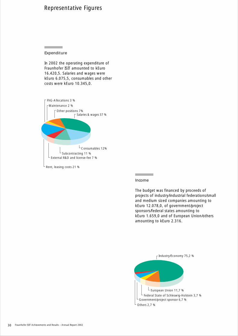
Expenditure
In 2002 the operating expenditure ofFraunhofer ISIT amounted to kEuro16.420,5. Salaries and wages werekEuro 6.075,5, consumables and othercosts were kEuro 10.345,0.
Representative Figures
Others 2,7 %
Government/project sponsor 6,7 %Federal State of Schleswig-Holstein 3,7 %
European Union 11,7 %
Industry/Economy 75,2 %
Income
The budget was financed by proceeds of projects of industry/industrial federations/smalland medium sized companies amounting tokEuro 12.078,0, of government/project sponsors/federal states amounting to kEuro 1.659,0 and of European Union/othersamounting to kEuro 2.316.

Fraunhofer ISIT Achievements and Results – Annual Report 2002 31
StrategicInvestments
OperatingInvestments
Project relatedInvestments
1.5001.0005000
Project related InvestmentsOperating InvestmentsStrategic Investments
Scientists
Graduated/technical staff
Administrationstaff
External scientists
Scientific assistance
Apprentice
0 5 10 15 20 25 30 35 40 45 50
Capital Investment
In 2002 the institutional budget ofcapital investment was kEuro 1.705,9.The amount of operating investmentwas kEuro 519,3, project relatedinvestments were amounted tokEuro 1.186,6.
Staff Developement
In 2002, on annnual average the staff constisted of 95 employees. 47were employed as scientific personnel, 36 as graduated/technical personneland 12 worked within organisationand administration. 1 scientists, 20 scientific assistents and7 apprentice supported the staff asexternal assistance.
32 Fraunhofer ISIT Achievements and Results – Annual Report 2002
RostockItzehoe
Bremen
Hamburg
Berlin
CottbusTeltow
Golm
Magdeburg
Halle
Dresden
ChemnitzJena
Ilmenau
WürzburgErlangen
Nürnberg
Wertheim
Braunschweig
Hannover
OberhausenDortmund
SchmallenbergDuisburg
AachenSankt Augustin
Euskirchen
Frankfurt
Darmstadt
St. Ingbert
Saarbrücken
Kaiserslautern
PfinztalKarlsruhe
Stuttgart
Freiburg
Efringen–Kirchen
Freisingen
München
Holzkirchen
Paderborn
Locations of the Research Establishments
The Fraunhofer-Gesellschaft
The Fraunhofer-Gesellschaft undertakes appliedresearch of direct utility to private and publicenterprise and of wide benefit to society. Its services are solicited by customers and contractual partners in industry, the service sectorand public administration. The organization alsoaccepts commissions and funding from Germanfederal and Länder ministries and governmentdepartments to participate in future-orientedresearch projects with the aim of finding innovative solutions to issues concerning theindustrial economy and demands faced by society in general.
By developing technological innovations andnovel systems solutions for their customers, the Fraunhofer Institutes help to reinforce the competitive strength of the economy in theirlocal region, and throughout Germany andEurope. Through their work, they aim to promotethe economic development of industrial society,paying particular regard to social and environ-mental concerns. As an employer, theFraunhofer-Gesellschaft offers a platform thatenables its staff to acquire the necessary profes-sional and personal qualifications to assume positions of responsibility within their Institute, inindustry and in other scientific domains.
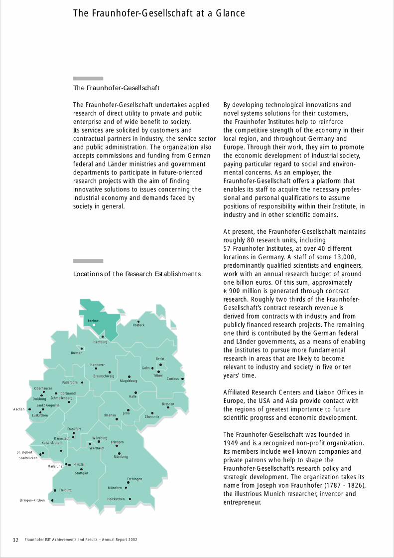
At present, the Fraunhofer-Gesellschaft maintainsroughly 80 research units, including57 Fraunhofer Institutes, at over 40 differentlocations in Germany. A staff of some 13,000,predominantly qualified scientists and engineers,work with an annual research budget of aroundone billion euros. Of this sum, approximatelyF 900 million is generated through contract research. Roughly two thirds of the Fraunhofer-Gesellschaft’s contract research revenue is derived from contracts with industry and frompublicly financed research projects. The remainingone third is contributed by the German federaland Länder governments, as a means of enablingthe Institutes to pursue more fundamental research in areas that are likely to become relevant to industry and society in five or tenyears’ time.
Affiliated Research Centers and Liaison Offices inEurope, the USA and Asia provide contact withthe regions of greatest importance to futurescientific progress and economic development.
The Fraunhofer-Gesellschaft was founded in1949 and is a recognized non-profit organization.Its members include well-known companies andprivate patrons who help to shape theFraunhofer-Gesellschaft’s research policy andstrategic development. The organization takes itsname from Joseph von Fraunhofer (1787 - 1826),the illustrious Munich researcher, inventor andentrepreneur.
The Fraunhofer-Gesellschaft at a Glance

Representative Results of Work

Super Junction Devices for High VoltagePowerMOS
Most of power switching applications in the voltage range up to 200 V are covered byPowerMOS transistors. The conduction loss andthus the On-resistance of a PowerMOS transistorincreases with higher blocking voltage require-ments. Under blocking conditions, a lower driftzone doping concentration is necessary to allowthe space charge region to expand without elec-trical break down. But the lowering of thedoping concentration also increases the driftzone resistance and therefore increases the con-duction losses.
In order to overcome this physical effect and toincrease the possible voltage range forPowerMOS transistors the so called “SuperJunction” (SJ) device was proposed. The principleis based on charge compensation by vertical p-doped columns realized in a n-doped drift zoneas shown in figure 1. Under blocking conditionthe entire volume in-between the p-bopedcolumns has to be fully depleted. By this appro-ach it is possible to increase the concentration ofthe n-doped drift zone without lowering themaximum break down voltage. Here the criticalparameters are the depth and distance as well asthe doping concentration of the p-dopedcolumns. By appropriate adjustment of thoseparameters it is possible to increase the concen-tration of the drift zone by e.g. a factor of ten.
This means Super Junction PowerMOS transistorsshowing improved conduction behaviour withlower On-resistance.
Up to now there is only one type of SJ-device(CoolMOS) available at the market. The technological approach is based on multi epitaxial Si growth for the built up of the p-doped columns.In contrast ISIT is developing an alternativemethod for the realisation of the p-dopedcolumns which is based on dopant outdiffusionfrom a boron glass deposited along the egdes ofdeep trenches.
In order to demonstrate the blocking capabilityof a SJ-device simulations have been carried outfor different depths of the p-doped regions.From the simulated diode characteristics shownin figure 2 it is obvious that PowerMOS applica-tion a trench depth (p-column) of 60 µm is requi-red with a drift zone concentration of 1015 cm-3.
Representative Results of Work:IC Technology
34 Fraunhofer ISIT Achievements and Results – Annual Report 2002
Deep trenchp column
MOS trench
n drift zone
n+ substrate
voltage [V]
curr
ent
[A] -9
1200 1000 800 600 400 200 0
-10
-11
-12
-13
100 µm 60 µm 40 µm 20 µm
Figure 1: Schematic of a Super Junction trench PowerMOS transistorwith p-doped columns within the n-doped drift zone.
Figure 2:Calculated diode characteristics for a substrate concentrationof 1015 cm-3 and trench depths of 20 µm, 40 µm, 60 µm and 100 µm respectively. Compared to a planar p-n junction,the breakdown voltage increases from approx. 270 V toabout 1000 V at a trench depth of 100 µm.

Compared to standard devices the bulk concen-tration level is one order of magnitude higher. Incase of PowerMOS transistors this would result in significant lower On-resistance.
To fabricate Super Junction structures, deep silicon trenches with smallest possible openingshave to be provided. For this purpose, the so called Bosch-process, which is mainly used forMEMS applications, was optimized. For trenchopenings in the micron range, depths up to60 µm were achieved. The side wall roughnessand the CD-loss both are less than 30 nm and100 nm, respectively. This roughness is removedby an oxidation step with subsequent wet etch inbuffered oxide etch.
The required boron concentration of the p-dopedcolumns is in the range of 1016 cm-3. The commonly used technique to achieve this dopingconcentration is ion implantation. However, ionimplantation is not recommended since thetrench side walls have to be doped also which becomes critical in case of high aspect ratio trenches. In order to realize the required dopinglevel a highly doped boron glas based on BBr3 orboron nitride was deposited on an oxide which iscovering the side walls of the trenches. Since theboron glas behaves as an unlimited doping sourcespecial diffusion processes were needed in orderto reach the specified doping concentration of
1016 cm-3 for the p-columns by outdiffusion. Thedoping profiles for the p-doped columns aredisplayed in figure 3. The profiles have beenmeasured by spreading resistance probe for different outdiffusion temperatures in the rangeof 1000 °C - 1200 °C. By appropriate adjustmentof the thermal budget for the outdiffusion process the required doping profile can be tailored.
The filling of the trenches is realized by Poly-Sideposition with a LPCVD process. As depicted infigure 4 conformal step coverage and excellentfilling behaviour have been achieved even fortrench depths of 60 µm.
In a next step first SJ-devices will be fabricatedfor design rule verification. The geometrical rules like pitch and depths of the trenches haveto be correlated with doping profiles of p-columns and drift zone in order to reach thecharge compensation requirement for a specifiedbreakdown voltage.
Fraunhofer ISIT Achievements and Results – Annual Report 2002 35
depth [µm]
con
cen
trat
ion
[1/
cm3 ]
51,0E+13
43210
1,0E+14
1,0E+15
1,0E+16
1,0E+17
1,0E+18
1,0E+191100 ºC
1000 ºC
1200 ºC
1150 ºC
Figure 3:Doping profiles measured by preading resistance probefor different outdiffusion temperatures.
Figure 4: Filling of 60 µm deep and 2 µmwide trenches with poly-silicon.20 µm

Representative Results of Work:IC Technology
36 Fraunhofer ISIT Achievements and Results – Annual Report 2002
Figure 2Top view of chip capacitors 20 mils by40 mils in size. The outer terminationis defined by solder bumps.

Fraunhofer ISIT Achievements and Results – Annual Report 2002 37
Passive Components: High precision chip-capacitors for GHz-application
The implementation of resistors or capacitors intostandard IC-processes is quite common and beingused since many years. In typical IC-processesresistors and capacitors are defined by dopedpoly-Si or diffusion regions and intermetal orinterpoly-Si dielectrics, respectively. The tolerancevalues are mainly related to the layer thicknessuniformities and the geometrical pattern transferprecision by lithography and etch structuring. Instandard IC-processes the tolerances of passivedevices are typically in the 5 - 10 % range.
The special capacitors discussed here are focusedon RF-applications for e.g. mobile phones andcontactless smard cards. Here the use of highprecision and high Q-value capacitors is mandatoryfor antenna impedance matching in order toavoid costly trimming of the device. Also, highself resonant frequency SRF is a further require-ment by minimizing L-C parasitics with advancedassembly techniques.
a solderable Cu-layer on top. The low-k passivationis specified for low pin-hole density and preventionof lateral solder diffusion along the capacitancetop plate. The outer termination of the device isrealized by solder bumps based on solder pasteprinting and reflow. The capacitor is designed forupside down flip chip assembly on printed circuitboards. With geometrical dimension of 20 by40 mils (approx. 500 x 1000 µm) a capacitancerange of 0.2 pF up to 180 pF have been reached.For smart card applications the devices are thin-ned down to 150 µm compared to a standard thickness of 320 µm. The typical appearance ofcapacitor devices with solder bump termination is illustrated in figure 2.
For practical application the capacitance stabilityversus frequency as well as a high Q- and SRF-value are of most importance. Especially thecapacitance value shows an excellent stability upto 3 GHz, compared to other leading RF-devices.The performance of the Q-value is excellent also, reaching more than 20 at a frequency of3 GHz. The RF-capacitor performance in terms ofcapacitance stability and Q-value versus frequencyis displayed in figure 3.
The fabrication of chip–capacitors for RF-appli-cations is based on standard semiconductor processes. Compared to other technologies chipcapacitors are beneficial in term of cost efficientfabrication methods, high reproducibility withtight tolerances and flexible for product variations.
SolderPassivationConductorDielectric
Figure 1:Cross sectional drawing of a chipcapacitor with solder bumps.
Frequency (Hz)
CapacitanceQ-Value
Cap
acit
ance
(p
F) 9,0
0,0E+00
Q-V
alu
e
8,8
8,6
8,4
8,2
8,0
1,0E+09 2,0E+09 3,0E+09
1
10
100
1000
10000
Figure 3Characteristic of capacitance and Q-value versus fre-quency for a RF chipcapacitor with nominal 8.5 pF.
The device principle is shown in the cross sectionaldrawing of figure 1. The base plate of the capaci-tor is defined by a highly doped Si-substrate withSiO2 as the dielectric layer on top. Depending onthe capacitance value used the oxide thickness isvaried in the range of 50 - 2500 nm with a min-max tolerance of +-1 %. The top plate of thecapacitor consists out of a 3 layer metal stack with

Patterning of Magnetic Hard Disks with Ion-Projection
The rapid increase of areal storage densities in magnetic hard disk drives may in future belimited by the thermal instability of small magnetic domains which is known as super-paramagnetism. Storage media featuring magnetically independent bit cells consistingof prepatterned single magnetic domains would allow to further postpone this limitation.
Patterning of these nano magnetic dots by usingion irradiation of an ion projection system wasthe aim of a research activity between companies:IBM, IMS-Vienna, Leica-Jena, together with research institutions: IMS-Chips Stuttgart andFraunhofer-ISIT.
Representative Results of Work:IC Technology
38 Fraunhofer ISIT Achievements and Results – Annual Report 2002
stencil mask 1” disk
4x ion-opticalreduction
Ar+ beam
ion source
Figure 2:Ion projection direct structuring (IPDS)for patterned magnetic media.
Figure 1:IBM microdrive disk.
Co/Pt multilayer thin films with strong perpen-dicular anisotropy and out-of-plane coercivities of5-11 kOe were magnetically altered in areas oflocal ion beam interaction. The ion irradiationswere performed by ion projection through siliconstencil masks fabricated by silicon on insulator(SOI) membrane technology. The ion projector atISIT was operated at 73 keV ion energy and witha 8.7-fold demagnification. Different ion species(He, Ne, Ar, Xe) have been used. Magneticislands smaller than 100 nm in diameter wereresolved in the Co/Pt films by means of magneticforce microscopy.
Monte-Carlo simulations of the intermixing process with the T-dyn software code resulted in

the required ion doses to create predefined losses of Co at the Co/Pt multilayer interfaces.The amount of these Co vacancies is responsiblefor the reduction of coercivity giving the necessarymagnetic contrast. The simulation predicted thatthe intermixing efficiency of 73 keV Ar+ ions is100 times stronger compared to 73 keV He+ ions.This has been confirmed by experiment and subsequent evaluation of the Co/Pt films by meansof magnetic force microscopy.
Using the ion projection technique concentricdata tracks including head positioning servoinformations were patterned onto a 1” glass disk as used in the IBM microdrive™ which was coated with Co/Pt multilayers. In a single
exposure step multiple tracks within an exposurefield of 17,5 mm in diameter were structured by 4 x 10¹³ Ar+/cm2 at 45 keV using a 4 - folddemagnification.
The high intermixing efficiency of Ar+ or Xe+ ionsand the high speed parallel pattern transfer of ion projection give a significant advantagewith respect to machine throughput which willbe mandatory for an economic mass fabricationprocess for prepatterned magnetic media.
This work has been supported by the GermanMinistry of Education, Science, Research, and Technology (BMBF) under grant number13 N 7837.
Fraunhofer ISIT Achievements and Results – Annual Report 2002 39
depth / arb.un.
ato
ms
200
1000
0
73 keV Ar→3.Layer
2000
3000
4000
5000
6000
7000
8000
40 60 80 100
73 keV Ar→7.Layer
Dose 0
Dose 6 x 1013 cm-2
PtCo
ion energy (keV)
do
se (
ion
s / c
m2 )
0
1E13
H
1E14
1E15
1E16
1E17
100 200
He
Ne
Ar
XeAu
Figure 3:T-Dyn simulation of ion intermixing of 10 Å platinum / 3 Åcobalt sandwich layers. Plotted are the atom dstributions ofthe 3rd and 7th sandwich layer after bombardment with adose of 6 x 10¹³ A+/cm2 at 73 keV energy. The number ofatoms correspond to an atomic mono layer within an area of500 nm2.
Figure 4:Ion doses for different ion species and energies leading to thesame degree of ion intermixing, revealed by T-dyn simulations.The intermixing is defined by the cobalt-concentration at the5th interlayer (in the middle of the stack, 82 Å below the surface) beeing reduced to 80 %.
Figure 5:Magnetic force microscopyof IPDS exposed tracks onmicrodrive disk. 45 keVargon ions; exposure dose4x1013 ions/cm2.
1¨µm
90 nm

Study on Bistable Thermomechanical Drives
Since the introduction of thermomechanical drives to MEMS in 1988 different applicationshave been proposed. Thermally driven microactators have been realised up to now normallyfor the construction of micro devices whichrequires a maximum of force. Typical examplesare micro valves and micro switches. Beside the simple construction and process integration, the generation of highmechanical forces and large actuation distancesare great advantages of these kind of micro actuators. Despite of the big advantages of thermoelectrically drives, the specific restrictionsof this kind of driving principles inhibits veryoften their use.
Since these devices consumes an electrical powerof at least 200 mW (micro switch) up to 1000 mW(micro valves) in the “on” stage, those devicescould be used only in some applications. Due tothe large thermal energy dissipation array arrange-ments and small area devices could be not realised.
A bistable approach can overcome these limits. In these concepts only during the short switchingperiod the power is necessary. In our concept the bistable behaviour is achieved by using anadditional actuator which clamps the switchingdevice in the on stage. (Project: MELODICT funded by the EC, project number: IST-1999-10945)The use of two actuators in one µ-relay offersthe opportunity to combine both, large strokelength and high contact forces. The arrangementof the two actuators allows the construction ofµ-relay which could be fixed in two stable stageswithout further power consumption. Thereforethe µ-relay requires only electrical power duringthe switching cycle.
The complete relay consists of two thermally driven actuator, the first actuator moves horizontally over the surface while the secondactuator moves perpendicular to the surface upand down. Both actuator are arranged in a way,that the lateral actuator can be moved under the activated vertical actuator and can be clamped by the vertical actuator when this actuator moves downwards.
The electrical contacts are located beside the vertical actuator and can be closed by the clamped lateral actuator. (z-actuator figure 1).
For switching the µ-relay into the on stage, bothactuators will be activated. Therefore the centralplate of the lateral actuator will be moved underthe central plate of the vertical actuator (figure 2).
For complete closing the electrical contacts thevertical actuator will be switched off and movesdownwards to the substrate and clamps the lateral actuator on the contacts. Finally the lateralactuator can be also switched off (figure 3).
For switching into the off state also both actuators will be first activated but switching offwill start with the lateral actuator. The movementof the lateral actuator into the initial positionopens also the electrical contacts.
Representative Results of Work:Microsystems Technology
40 Fraunhofer ISIT Achievements and Results – Annual Report 2002
Figure. 2:Centre area of a µ-relay. The complete µ-relay consist of two actuators, the firstactuator moves laterally over the substrate surface, the second actuatormoves vertically up and down.

Due to the use of two actuator relatively largestrokes of the relay can be combined with a highcontact forces. For the calculations a modelbased on the model of a double side clampedbridge was used. Using the lateral actuator arelay stroke of up to 60 - 70 µm has been measured, while contact forces which are generated by the vertical actuator of 10 - 15 mNper contact are achieved. The required chip area for realising both micro actuators is about0.5 mm x 2.5 mm, and therefore as small as the smallest electrostatically driven µ-relays.Depending from the accurate dimensions of the relay switching time faster than 25 ms and apower consumption of lower than 200 - 300 mWduring switching are possible. The electricalpower is only required during switching.
Fraunhofer ISIT Achievements and Results – Annual Report 2002 41
clamping actuatorsignal lineslateral actuatorheater
Figure 1:3D-view of the µ-relay. The complete µ-relay consist of twoactuators, the first actuator moves laterally over the substratesurface, the second actuator moves vertically up and down.Both actuators are thermally driven by a heater locatedunder the nickel structures. The µ-relay is here shown in theon-state.
Figure. 3: The picture shows a clamped lateralactuator by the vertical one. In thisexample the lateral contacts are closedby the actuator.

Glass Flow Process GFPA Novel Micromachining Technology forStructuring Borosilicate Glass Substrates
For the manufacturing of microstructured glasssubstrates a novel clean room compatible micromachining process technology has beendeveloped. With this Glass Flow Process (GFP),which is based on viscous deformation at temperature above the glass transition temperature Tg, any surface topography available on a silicon substrate, like e.g. micro-fluidic channel structures (figure 1), can be moulded into bondable alkali-borosilicate glasses.Beside complete replication of silicon structuresinto glass this technique allows also the fabrica-tion of optical micro lens arrays with high aspectratios and minimal spacings (figure 2).
The GFP technology is based on standard MEMSprocesses (figure 3). First a pattern is etched into silicon using deep reactive ion etching(DRIE). Then an alkali-borosilicate substrate(Schott BOROFLOAT®33) is hermetically sealed tothe silicon preform by anodic bonding undervacuum. The bonding process is followed by anannealing step in an atmospheric furnace system.The temperature for this GFP step is typically well above the glass transition temperature of Tg = 525°C. Thus, the viscosity of the glass isdrastically lowered. The pressure difference leadsto slumping of glass material into the silicon cavity(figure 4) until the cavity is completely filled so
the original silicon topography is moulded intoglass. The minimum feature size as well as thestructure height is hereby limited only by the previous silicon structuring process. Finally thesilicon wafer is removed by wet etching and thebackside of glass substrate is mechanically planarized.
If the slumping process is stopped before reachingthe bottom of the cavity, the resulting shape ofthe glass surface is spherical and can be used asa microlens. These lenses can be fabricated withhigh aspect ratios and central heights up to200 µm without costly and time consuming dry etching of glass substrates. This contactlessforming process results in a very low surfaceroughness. The resulting lens profiles are cha-racterised by line scan measurements and show aslight elliptical deviation in the outer region ofthe lenses. All relevant optical parameters aresummarized in table 1.
Introducing this GFP technology to MEMS processing enables the deep structuring of glass
Representative Results of Work:Microsystems Technology
42 Fraunhofer ISIT Achievements and Results – Annual Report 2002
Figure 1: Microfluidic channel structures in boro-silicate glass: substrate with step heightof 150 µm and minimum channelwidth of 20 µm.
Table 1: GFP microlens specification.
lens material alkali-borosilicate glass(Pyrex, Borofloat)
refractive index n n = 1,473
lens radius rL
lens height hL
lens profileminimal spacing
5 ... 5000 µmup to 500 µmspherical, parabolic10 µm
optical transmission 325 ... 2600 nm
focal length uniformity ∆fsurface roughness rmslens abberationlateral adjustment accuracy
< 2,5 %< 2,5 nm< λ/2< 1 µm

substrates and opens up a wide range of newapplications. Since whole glass substrates can befabricated by this new technique completemicrooptical stacks can be mounted by anodicbonding of silicon and microstructured glasswafers. New types of optical packaging solutions or complete stacked microoptics can berealised in this new process.
Fraunhofer ISIT Achievements and Results – Annual Report 2002 43
Figure 2: With GFP technology the highvolume manufacturing of densemicro lens arrays with highaspect ratios is possible (lens radius rL = 270 µm, lens height hL = 65 µm).
MEM
S Pr
oce
ss
GlassFlow Process
Resist OxideSi Substrate
LithographyRIE Oxide
Si HRIE
AnodicBonding
Si GrindingTMAH Wet Etch
Figure 3: All GFP technolgy steps are basedon standard MEMS processes.
TGFP
Pi < Pa
Si
Glass
Pa
Glass
Si
Pa
TGFP
Figure 4: Schematic (left) and actual SEM picture (right) before and after the thermal treatmentof the bonded glass-silicon stack. The glass forming takes place at temperatures wellabove Tg, where the viscosity of the borofloatglass is drastically lowered. The pressuredifference between silicon cavity (vacuum) and oven atmosphere (~1 bar) leads to acontinuous movement of the glass material: the interfacial glass surface slumps intothe silicon cavity.

Silicon Etching of Deep Trenches with High Aspect Ratio
The utilisation of deep silicon etching in MEMSand IC-Technology becomes more and moreimportant for various device purposes. For MEMSdeep reactive ion etching (DRIE) is already beenused mainly for surface mechanical applicationsin the field of sensoric, actuatoric and micro-optical components. Also for IC-Technology newdevice architectures are taking advantage ofdeep trenches for e.g. lateral isolation, trenchpower devices, passive components and DRAMapplications. Typical requirements for the etchingof deep trenches in Silicon are ranging from tens-up to hundreds of microns. The use of conven-tional Silicon dry etch processes based on chlori-ne or bromine chemistry attain nearly verticalstructures, however the achieved etch rates aretypically in the order of 200 nm/min only. Thoseetch rates are insufficient for deep trench etchingin mass production.
Applying dry etch processes using fluorine chemistry etch rates in the range of microns perminute are reached. Here, the etch process suffers from low selectivity against resist and silicon oxide at room temperature. The well-knownBosch-process is characterized by alternating etchand polymer deposition cycles. Both, high etchrates and high selectivities against the maskinglayers were achieved in this case.
In standard MEMS applications the so calledBosch-process is utilized to generate structureswith dimensions of several tens of microns. For this purpose the process induced sidewall
roughness of about 200 nm and a CD-loss in therange of microns is tolerable. For more advancedapplications with structures in the micron andsub-micron range, those CD-variations are notacceptable. Aiming at these dimensions ISITimproved the Bosch-process for high aspect ratiodeep trench etching in the sub-µm regime. Fortrench openings in the µm-range we achieve aside wall roughness and a CD-loss of less than30 nm and 100 nm, respectively. In the sub-µmrange the losses are less than 20 nm. Moreover,we enabled the control of the side wall slopefrom nearly vertical to a conical profile, which isimportant for trench filling purposes.
The work performed at ISIT demonstrates thepossibility to etch trenches with aspect ratios upto 60:1. Figure 1 shows trenches of 1 µm and2 µm widths with vertical and conical profilesetched with an improved Bosch-process. Especially DRIE for trenches with dimensionsdown to 0.4 µm has to be highlighed as shownin figure 2. It has to be mentioned that specialetching strategies are required to achieve thoseexcellent results. In our experiments the criticaldimension was limited by lithografic resolution. Itis expected that the etch process has the potenti-al to be used for further down scaling of geome-trical dimensions.
With the availability of a DRIE process for highaspect ratio Silicon structuring in the sub-µmrange a powerful tool for the development ofnew device architectures is provided.
Representative Results of Work:Microsystems Technology
44 Fraunhofer ISIT Achievements and Results – Annual Report 2002
Figure 1: DRIE for Silicontrenches of 1 µmand 2 µm widthswith vertical andconical profiles.
Figure 2:DRIE for Silicontrenches of 0.4 µm,0.5 µm and 0.6 µmwidths with aspectrations up to 60:1.
1 µm
2 µmvertical
2 µmconical
0.4 µm0.5 µm
0.6 µm

Access to Microsystem Production, Co-operation within EUROPRACTICE
New products based on microsystem technologies(MST) lead to an annual growth rate of the MSTmarket that is comparable to the growth rate ofthe world-wide semiconductor market (on average15-20 % p.a.). Since the overall MST market stillamounts to approx. 10-15 % of the semiconductorturnover, this high growth rate makes Microsys-tems to a very promising market. Additionally, inmore and more areas MST is becoming a majorenabling technology that is decisive for the intro-duction of new and advanced products and servi-ces. The actual development of MST markets willbe determined by how accessible that technologywill be to the user community, how well thesetechniques can be transferred into new productsand how many engineers are skilled and expe-rienced enough to apply these new techniques.
Since several years the European Union is supporting the transfer of MST developmentsinto actual new products and services. Togetherwith Bosch and HLPlanar ISIT is partner in theproject AMICUS to offer manufacturing servicesfor new Microsystems.
Within AMICUS the following activities have started:• Providing a market- and product-oriented
access to Microsystems technology. A definedroute from first prototypes to a product isgiven and the customer is accompanied onthis way. Standardised technologies and processes are offered for product developmentwithin a reasonable time. Hence, small andmedium-sized enterprises can rely on well-proven processes and may concentrate on thefunctionality and application of their devices.
• Adding new developments in the productionprocesses to the existing services. Ongoingprojects as well as new users can profit fromthese adjustments by reaching a higher accuracy and quality level of their systems.
• Supporting users in the development of complete systems beyond the underlying functionality of the device. The knowledge of
the EUROPRACTICE partners helps the customers to expedite the market introductionof their products and to adjust their develop-ments to dedicated applications.
• Using established process steps for the generation of a new standardised processsequence. Once a standard flow is established,new products can be developed and intro-duced to the markets.
The AMICUS project and the work of ISIT as acompetence centre in sensor technologies isaiming to accelerate the uptake of existing andemerging microsystem technologies in new marketareas by combining existing MST manufacturingand application Know How. Meanwhile ISIT couldrealise several new contracts for technical studies,MST prototyping and production transfer. In2002 the AMICUS activities during fairs andworkshops have lead to five new contracts.Several promising contract negotiations are stillongoing and will finally lead to additional projects. Also customer support starting fromapplication knowledge in the field of physicalsensors that is organised within ISIT in the EUROPRACTICE part of a competence center hasalready initiated several new industrial projects.
Fraunhofer ISIT Achievements and Results – Annual Report 2002 45
Maintenance at semiconductor process equipment.

Representative Results of Work:IC-Design
46 Fraunhofer ISIT Achievements and Results – Annual Report 2002
Figure 1:Graphical user interface (GUI) of the cross-section viewerintegrated in the realized design-kit.

Fraunhofer ISIT Achievements and Results – Annual Report 2002 47
Design-Kit for Microsystem Designers
Modern design of ICs is established since twodecades in a way that designers use design-kits,distributed by the IC-fab of choice, to realize theelectronics. The design-kit is a software add onwritten for one of the IC-design software packages,that includes specific data of the technologiesthe IC-fab offers. In the beginning there wereonly the technology file with the names of thelayers, the design rules for the DRC and theparameters of the models. Nowadays design-kitsare more complex, often the complete enviro-ment of the IC-design software is adapted andincludes design examples, all kinds of documen-tations (.html or .pdf), tutorials for beginners,parameterized cells, and a set of verification tools.
With the first MST-fabs the idea to provide sucha tool available for MST-designers is covered toaccelerate the design and lower the hurdles forfirst-time users. The development of such adesign-kit is part of the European project MEM-SOI2 (IST-2001-33443) for the MST-fab Tronic’s inFrance for their optical SOI technology.
The tool is fully integrated within the designenvironment of CADENCE‚ and includes a variatyof special add ons which accelerate the design-
flow from idea to final maskdesign. The design-kit simplifies a couple of design steps with amore intuitive graphical user interface based onthe specific technological process. A cross-sectionviewer allows a general insight into the processto check the functionality of the particular device.
A number of parameterized layout cells (p-cell)like bars, massive and perforated blocks, roundplates are available to create the design in anextremely flexible way. In a further step those special p-cells will include additional informationthat allows an easy-to-use interaction betweenthe design environment and the mechanicalFEM-simulator (ANSYS). Based on the processrelated material properties (youngs modulus,density, ...) and the geometrical data of the masklayout a software-interface has been realizedwhich allows users to perform a stress and modalanalysis with ANSYS‚ by simply click on a singlebutton.
Due to the fact that the design-kit is directly integrated within the CADENCE environment byusing its own programming language SKILL, theentire size of the software package is minimizedto a couple of 100 kBytes only. Professional licen-sing and user-friendly installation is included, too.
Figure 2:Layout data from Cadence cansimply be imported into Ansysin order to run FEM analyses.
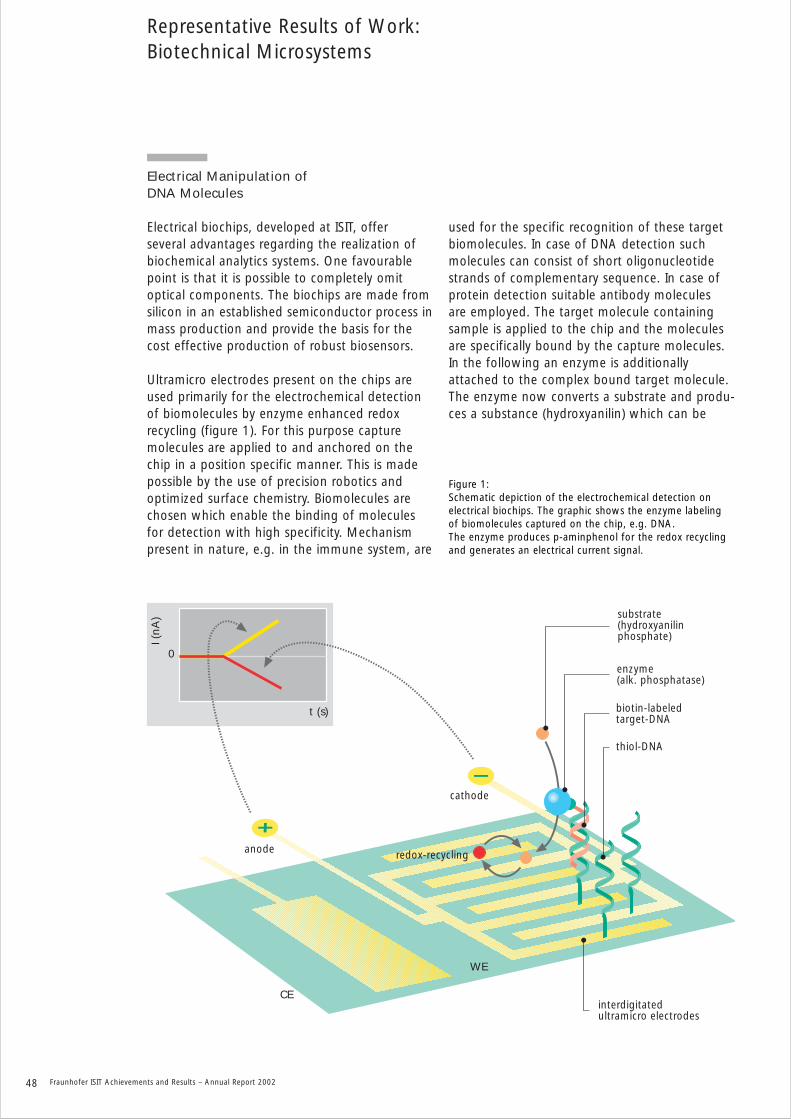
Electrical Manipulation of DNA Molecules
Electrical biochips, developed at ISIT, offer several advantages regarding the realization ofbiochemical analytics systems. One favourablepoint is that it is possible to completely omitoptical components. The biochips are made fromsilicon in an established semiconductor process inmass production and provide the basis for thecost effective production of robust biosensors.
Ultramicro electrodes present on the chips areused primarily for the electrochemical detectionof biomolecules by enzyme enhanced redox recycling (figure 1). For this purpose capturemolecules are applied to and anchored on thechip in a position specific manner. This is madepossible by the use of precision robotics andoptimized surface chemistry. Biomolecules arechosen which enable the binding of moleculesfor detection with high specificity. Mechanismpresent in nature, e.g. in the immune system, are
used for the specific recognition of these targetbiomolecules. In case of DNA detection suchmolecules can consist of short oligonucleotidestrands of complementary sequence. In case ofprotein detection suitable antibody molecules are employed. The target molecule containingsample is applied to the chip and the moleculesare specifically bound by the capture molecules.In the following an enzyme is additionally attached to the complex bound target molecule.The enzyme now converts a substrate and produ-ces a substance (hydroxyanilin) which can be
Representative Results of Work:Biotechnical Microsystems
48 Fraunhofer ISIT Achievements and Results – Annual Report 2002
0
t (s)
I (n
A)
biotin-labeledtarget-DNA
substrate(hydroxyanilinphosphate)
enzyme(alk. phosphatase)
thiol-DNA
interdigitatedultramicro electrodes
anode
cathode
CE
WE
redox-recycling
Figure 1: Schematic depiction of the electrochemical detection onelectrical biochips. The graphic shows the enzyme labeling of biomolecules captured on the chip, e.g. DNA. The enzyme produces p-aminphenol for the redox recyclingand generates an electrical current signal.

detected in a highly sensitive electrochemicalreaction. The signal consist of an electrical current detectable by specialized electronics anddirectly suitable for computer compatible signalanalysis and evaluation. Here the interdigitatedstructure of the embedded gold electrodes onthe chip is a requirement for the sensitive detec-tion.
Beside the electrochemical detection principle the presence of electrodes on the silicon chipsenable additional new possibilities to activelycontrol the detection of biomolecules. These possibilities are based on the fact that some ofthe detected biomolecules are charged particles.DNA molecules as well as proteins exhibit a surface charge due to their composition andstructure. This charge can be used to manipulatethe molecules by applied electrical fields. DNA isnegatively charged and directed electrical fieldsmove the molecules toward the chip surface. Thisprocedure increases the local concentration ofDNA and therefore reduces the time needed forspecific binding (hybridization) and enhances thesensitivity in a given time frame. Vice versa acontrolled repulsion can be effective for enhan-cing the specificity (stringency) of the bindingreaction. Alternating electrical fields are used toprevent the generation of electrical double layers(figure 2). Both methods of attraction and repul-sion allow to speed up the sensitive detection ofbiomolecules with electrical biochips and make itmore specific as it would be possible with otherpassive biosensor systems.
Fraunhofer ISIT Achievements and Results – Annual Report 2002 49
25%
0 Hz 1 Hz 10 Hz 100 Hz 1000 Hz
20%
15%
10%
5%
0%
30 seconds electr. field
60 seconds electr. field
rel.
flu
ore
scen
ce in
ten
sity
Figure 2: Fluorescence detection of manipulation of DNA by applyingalternating electrical fields. Two preset potentials are appliedalternating between the interdigital electrodes and the frequency of switching the potentials is being varied. Thealternating field enables the effective attraction of fluore-scence labeled DNA toward the electrodes.
The outlined technology was developed in the scope of the BMBF joint project SIBANAT. The project won the ”Jack Raper Award forOutstanding Technology Directions Paper” in2003.
Two preset potentials are applied alternating between the interdigital electrodes and the frequency of switching the potentials is beingvaried. The alternating field enables the effectiveattraction of fluorescence labeled DNA towardthe electrodes.

Portable Monitoring Systems for Protein Detection
ISIT continous to develop the electrical biochiptechnology platform for different applications inbiotechnology, medicine and the food industry.The available eBiochip devices are suitable tospecific DNA- and RNA-identification as well asto the protein identification. Proteins have to bedetected directly with high sensitive immunologi-cal methods because even smallest amounts ofbioweapon toxins are lethal for humans.
Due to the principle and functionality of theeBiochip it is possible not only to realize devicesfor specific identification of molecular species butalso to develop devices for monitoring air and
water for contamination (alarm function). Here acombination with magnetic bead technology isused.
The heart of the device is the electrical biochip. It is produced in silicon semiconductor technologyat ISIT and exhibits embedded interdigitatedmicro electrode arrays made in gold, which areshaped like fingers of two hands entangled intoeach other (figure 2).
For the specific detection of proteins a commonmethod called ELISA (Enzyme Linked Immuno-sorbent Assay is applied. Performing thismeasurement, biological capture molecules calledantibodies are fixed to microscopically small paramagnetic plastic beads.
Then those antibody-loaded beads are transportedin aqueous dispersion to the eBiochip device andcollected with the help of a controllable magneton the chip surface. If target molecules are present in a sample, which is subsequentlybrought in contact with the beads, they will bindto the specific antibodies. The following electrochemical detection is based on the redox-
Representative Results of Work:Biotechnical Microsystems
50 Fraunhofer ISIT Achievements and Results – Annual Report 2002
Figure 1: Mounted elec-trical biochip.

Fraunhofer ISIT Achievements and Results – Annual Report 2002 51
recycling of hydroxyanilin, which is produced bya label enzyme, which is only bound if a target-capture complex was formed. After the removalof the magnet and the flushing of used beads thebiochips can be used for new rounds of detec-tion cycles with fresh antibody-loaded beads.This procedure enables a semi-continuous identi-fication and monitoring (alarm function) of toxins
using a chip for more than two weeks.Due to the high sensitivity of the detection principle the eBiochip device was able to reachdetection limits in the femtomolar range. A concentration of 0,5 - 10 ng/ml of several bioweapon toxins e.g. staphylococcus enteroto-xin type B (SEB), botolinum toxin type A has beendetected as can be seen below.
Figure 2: Details of interdigitated embed-ded electrodes of 0,7 µm width.
ng/ml SEB
curr
ent
slo
pe
[nA
/min
]
30
20
25
15
10
5
0 1 3 100
Figure 3: Sensitivity range of electricalmonitoring of SEB.

Low-Profile and Flexible Electronic AssembliesUsing Ultra-Thin Silicon
Today there is a strong trend towards thin andflexible packages which is driven by differentindustrial applications e.g. smart cards and electronic labels. Furthermore, several technicalapproaches for ultra-thin chip stacking leading to3D assemblies are followed, see table 1. The motivation to use ultra-thin silicon is low-pro-file assemblies, flexible (bendable) assemblies and the enhancement of device performance e.g.in power electronics. In the European IST ProjectFLEX-SI (”Ultra-thin packaging solutions usingthin silicon”, IST-99-10205) the eight partnersPhilips Semiconductors (A), W.S.I. (F), Datacon (A), Nokia (FIN), Oticon (DK), PAV CARD(D), Helsinki University of Technology (FIN) andFraunhofer ISIT (D) were working together on anindustrial approach of low-profile packaging with ultra-thin flexible Si chips with a thickness < 50 µm. The basic approach of the FLEX-SIProject is to adapt and optimise existing industrialprocesses and equipment for the use of ultra-thinsilicon instead of introducing totally different
processes which are not compatible to the presentinfrastructure. With this approach, the FLEX-SIProject has provided a complete flow of industrialprocesses for ultra-thin silicon packaging fromthe initial end-user wafers to functional systemswith low-profile modules.
Main results have been achieved in the following areas:• wafer thinning to 50 µm rest thickness
with complete de-stressing,• electrical testing of ultra-thin wafers
under static bending stress,• handling and shipping of ultra-thin wafers,• ultra-thin chip stacking for chip-on-chip
applications,• low-profile flip chip with pre-applied
no-flow underfill,• integrated module board (IMB)
technique with ultra-thin chips,• functional demonstrators working in
their system environment.
Representative Results of Work:Module Integration
52 Fraunhofer ISIT Achievements and Results – Annual Report 2002
Figure 1:Handling of ultra-thinwafer: wafer bow(left), film-frame carrier (right).

Handling concept for of ultra-thin wafersBased on the experience gained in the FLEX-SIProject is the use of flexible carrier based handling recommended. Here, standard filmframe carriers with selected UV adhesive tapes with reduced residual adhesion can beused. Figure 1 shows the bow of a 50 µm ultra-thin wafer without support and an ultra-thin wafer mounted on tape. To minimizehandling of bare ultra-thin wafers, the wafersshould be mounted on the film frame carrierdirectly after ultra-thinning at the thinning site.This can be done by an automated handler to avoid any hands-on steps. We recommendthat the dicing of the ultra-thin wafers is alsoperfomed at the thinning site as there are severaladvantages:
• know-how and experience in dicing of ultra-thin wafers but also in inspection of the dicingquality is available
• qualified UV exposure directly after the dicing• robust shipping and handling (low stress on
chip level)• defined interface for automated equipment• defined quality gateTwo important limitations of this concept shouldbe mentioned:• If a further processing of ultra-thin wafers is
necessary, e.g. implantation and backsidemetallization in power electronics, a rigid carrier concept is beneficial.
• Following the FLEX-SI handling concept, especially when the ultra-thin wafers are dicedat the thinning site, the user cannot performelectrical testing on wafer level after the thinning. Special testing equipment for dicedwafers on film frame carrier is available, butdoes not provide the performance of standardwafer tester (e.g. speed, backside contact).
Fraunhofer ISIT Achievements and Results – Annual Report 2002 53
Figure 2:8" wafer with 50 µm thickness(Philips Mifare®) afterdicing in ISIT.
Table 1:Technology drivers forultra-thin silicon.
• RF ID systems(smart cards, labels, tags)
• Portable systems(telecom, video, ...)
• Computer(memory modules)
• Mechatronics, MEMS,sensors
• Power electronics
Applications Technologies
• Flip chip on flex• Isoplanar interconnection• Chip embedding
(chip-in-board)• Chip stacking and
´folded´ stacks• Vertical integration• Chip-on-bent surface• Power modules
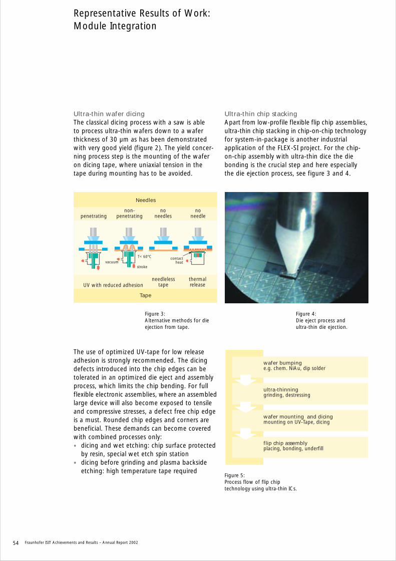
Ultra-thin wafer dicingThe classical dicing process with a saw is able to process ultra-thin wafers down to a waferthickness of 30 µm as has been demonstratedwith very good yield (figure 2). The yield concer-ning process step is the mounting of the waferon dicing tape, where uniaxial tension in thetape during mounting has to be avoided.
Ultra-thin chip stackingApart from low-profile flexible flip chip assemblies,ultra-thin chip stacking in chip-on-chip technologyfor system-in-package is another industrial application of the FLEX-SI project. For the chip-on-chip assembly with ultra-thin dice the diebonding is the crucial step and here especiallythe die ejection process, see figure 3 and 4.
Representative Results of Work:Module Integration
54 Fraunhofer ISIT Achievements and Results – Annual Report 2002
The use of optimized UV-tape for low releaseadhesion is strongly recommended. The dicingdefects introduced into the chip edges can betolerated in an optimized die eject and assemblyprocess, which limits the chip bending. For fullflexible electronic assemblies, where an assembledlarge device will also become exposed to tensileand compressive stresses, a defect free chip edgeis a must. Rounded chip edges and corners arebeneficial. These demands can become coveredwith combined processes only:• dicing and wet etching: chip surface protected
by resin, special wet etch spin station • dicing before grinding and plasma backside
etching: high temperature tape required
wafer bumpinge.g. chem. NiAu, dip solder
ultra-thinninggrinding, destressing
wafer mounting and dicingmounting on UV-Tape, dicing
flip chip assemblyplacing, bonding, underfill
UV with reduced adhesionneedleless
tapethermalrelease
penetratingnon-
penetratingno
needles
Tape
vacuumT< 60ºC
stroke
Needles
noneedle
contactheat
Figure 3:Alternative methods for dieejection from tape.
Figure 4:Die eject process and ultra-thin die ejection.
Figure 5: Process flow of flip chip technology using ultra-thin ICs.
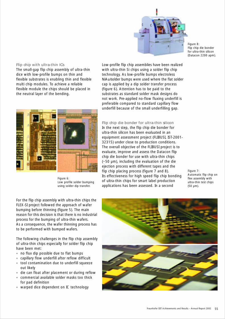
Flip chip with ultra-thin ICsThe small-gap flip chip assembly of ultra-thindice with low-profile bumps on thin and flexible substrates is enabling thin and flexiblemulti chip modules. To achieve a reliable flexible module the chips should be placed in the neutral layer of the bending.
Low-profile flip chip assemblies have been realizedwith ultra-thin Si chips using a solder flip chiptechnology. As low-profile bumps electrolessNiAu/solder bumps were used where the flat soldercap is applied by a dip solder transfer process(figure 6). Attention has to be paid to the substrates as standard solder mask designs donot work. Pre-applied no-flow fluxing underfill ispreferable compared to standard capillary flowunderfill because of the small underfilling gap.
Flip chip die bonder for ultra-thin siliconIn the next step, the flip chip die bonder forultra-thin silicon has been evaluated in an equipment assessment project (FLIBUSI, IST-2001-32315) under close to production conditions. The overall objective of the FLIBUSI project is toevaluate, improve and assess the Datacon flipchip die bonder for use with ultra-thin chips (~50 µm), including the evaluation of the dieejection process with different tapes and the flip chip placing process (figure 7 and 8). Its effectiveness for high speed flip chip bondingof ultra-thin chips for smart label productionapplications has been assessed. In a second
Fraunhofer ISIT Achievements and Results – Annual Report 2002 55
Figure 6: Low profile solder bumpingusing solder dip transfer.
Figure 7:Automatic flip chip onflex assembly withultra-thin test chips(50 µm).
For the flip chip assembly with ultra-thin chips theFLEX-SI project followed the approach of waferbumping before thinning (figure 5). The main reason for this decision is that there is no industrialprocess for the bumping of ultra-thin wafers. As a consequence, the wafer thinning process hasto be performed with bumped wafers.
The following challenges in the flip chip assemblyof ultra-thin chips especially for solder flip chiphave been met:• no flux dip possible due to flat bumps• capillary flow underfill after reflow difficult• tool contamination due to underfill squeeze
out likely• die can float after placement or during reflow• commercial available solder masks too thick
for pad definition• warped dice dependent on IC technology
Figure 8: Flip chip die bonderfor ultra-thin silicon(Datacon 2200 apm).

application, a solder die bond with ultra-thinchips for power modules is investigated. Figure 9shows the direct bonded copper (DBC) substrateassembled with ultra-thin power semiconductorsafter large wire bonding. The performance of theequipment has been evaluated under close toproduction conditions and assessed in terms ofprocess quality, yield, MTBF, MTTR, uptime,throughput and Cost of Ownership. As mainresult of the FLIBUSI project, it can be stated thatultra-thin die assembly technology is ready forproduction offering high speed processes (6000 uph for flip chip), high placement accuracy(< 10 µm/3 σ) and high yield (> 99 %), figure 10.The availability of automate equipment which is able to work with ultra-thin wafers resp. chipsis a key requirement for the wide industrial use of thinned silicon in different applicationsincluding identification systems, power electronics,
mobile telecommunication, computers, consumerelectronics and medical technology. The maingoal of the assessment project therefore is toenable enhanced use and performance of ultra-thin silicon by providing automated indus-trial equipment for chip and flip chip placementon substrates.
56 Fraunhofer ISIT Achievements and Results – Annual Report 2002
Figure 9: DBC substrate withultra-thin chips.
Figure 10:Placement accuracy offlip chip die bonderwith ultra-thin chips. Die number
x/y
off
set
(µm
)
(i) Chip placement accuracy X/Y15
10
5
0
-50
-10
-15
Y
X
Upper spec limit (3 s)
Lower spec limit (3 s)
SX = 1.50 µm
SY = 2.12 µm
Die number
Ro
tati
on
(m
º) 150
125
100
75
50
25
0
-25
-50
-75
-100
-125
-150
ST = 28,01mº
Theta
(ii) Rotation placement accuracy (0)

Business Opportunities for AdvancedPackaging in Europe
Together with three Partners (IZET Innovations-zentrum Itzehoe, Germany, MTA Marketing &Technologies Avancees, France and PP ProvencePromotion, France) ISIT developes a businessstudy about European packaging activities. This study is part of the project “Federating aPackaging and Interconnection TranseuropeanIndustrial Activity, PATRIA“ supported by theEuropean Commission (IST-2001-38482).
Vision The global aim of PATRIA is to help pave the wayfor the resurgence of industrial scale advancedpackaging and interconnection services in Europetargeting very advanced technologies, in close-ness to European semiconductor manufacturers,smart card industry and MEMS facilities.
Aims The aim of this study is to develop and to validatea plan for business opportunities in industrialscale advanced packaging and interconnectionservices in Europe, targeting very advanced tech-nologies, in closeness to the European semicon-ductor manufacturers, smart card industry andMEMS facilities and situated within a consumermarket of soon 500 million people with theexpected EU expansion toward Eastern Europe.
PATRIA validates this work, representing a dynamicspringboard to regain packaging business andindustrial activity, today lost to Asian vendors,through the consolidation of a plan for businessopportunities, building on emerging operations,attracting and federating industrial users, entre-preneurs and investors. PATRIA implements a modelof federation of the existing operations and incubation of sub-critical initiatives, stemmingfrom the existing research, commercial, industrial,political and governmental resources, in order toallow to reach the critical mass of what is conside-red as a capital intensive and competitive business.
Business Initiative Group ”BIG”A Business Initiative Group (BIG) has been set upconsisting of a ”who is who” in the field, which
is to convene on a number of occasions to allowhigh level decision makers to interact, discuss,and network toward realising new initiatives forEurope in advanced packaging and interconnection.Any organisation with hands on business in packa-ging, interconnection and assembly can join. TheBIG group will be operated in two phases: 1. devising a realistic strategy based on the
European position and capabilities in terms oftechnology, market needs, available resourcesand funding;
2. implementing this strategy.
The BIG group brings together a core of personsholding strategy and management positions within the European research, manufacture andfinancial and communities. Involved in the packa-ging, interconnection and assembly processes,primarily as users, or as innovative suppliers too,they contribute in two ways:• feed the study by their experience, vision of
the markets and technologies • hopefully become active players by imple-
menting part of the plan for business releasedwithin PATRIA, along with other BIG membersor by contracting alliances and partnershipswith other organisations.
That's the PATRIA ultimate objective: synergizethe wills of BIG members into new business.
Fraunhofer ISIT Achievements and Results – Annual Report 2002 57
Representative Results of Work:Module Integration
PATRIA´s choice ofAdvanced Packaging & Interconnection technologiesfor semiconductors, smart cards and MEMS
Single chipIC packaging
miniaturised SMT packages(Chip-Scale-Package, CSP)
incl. • wafer bumping for flip chip assembly • flip chip in package, • wafer-level CSP with ballingfocus: wafer-level chip sizepackage (WL-CSP)
Hybrid integratedmulti chip packaging
multi chip module (MCM) / systemin package (SIP):
• MCM/SIP for ICs with discrete or integrated passives • MCM/SIP for MEMS with ICs, passives • multi chip smart card module

Project ResultsThe continuous technical progress and pricedecrease of silicon integrated circuits, smart cardsand MEMS, in the direction of advanced systemintegration approaches, is accompanying the pervasion of consumer, computer and telecomproducts. Less known and visible is the considerable pressure that the IC technical progress - in term of physical volume, number ofinputs and outputs, power dissipation, operatingspeed - puts on the techniques and industrialoperations of packaging, interconnecting and assembling these ICs into cost-effective,small and affordable sub-assemblies. PATRIAaddresses this specific need, delivering a practicalaction plan for solid and sustainable industrialsupply of advanced packaging and intercon-nection solutions for the European industry in Europe federating the important stakeholdersin this area.
The important issues are:• Packaging and interconnection is becoming
more and more a crucial part of componentsand system industries (e.g. key to Bluetooth modules efficiency, costreduction & system business viability)
• System on a Chip issues can be (are) manytimes approached by system in a packagesolutions (e.g. Pentium, to quote only afamous one)
• Advanced packaging is difficult to outsourceto distant and low engineering suppliers
• The viability of an European business modelfor advanced packaging solutions (BGA, CSP, ...) has been demonstrated byAtlantis or Pac Tech
• This is usually considered as a very capitalintensive environment with rather low margins
• Interest in advanced packaging is combinedwith semiconductor industry cycles (of busi-ness and also of enthusiasm) and high indu-strial mobility (Moore's law, new fabs, globalscenarios, ...)
Representative Results of Work:Module Integration
58 Fraunhofer ISIT Achievements and Results – Annual Report 2002
Customer specific chip-size-packages with solderballs and BCB passivationbefore dicing.


rechargeable battery with graphite as anodematerial. An outstanding result is the cycle stabi-lity of the titanate system shown in figure 2. Butalso the low self discharge rate (reversible andirresversible) and the stability with respect todeep discharge are remarkable.
Hearing-Aids with Rechargeable Power Supply (HARPOS)
The number of people depending on hearing-aids is steadily growing due to the increasingnumber of (a) elderly people in our society and (b) younger people suffering from hardness of hearing due to strong noise exposure by modernentertainment tools and events. Conventionalhearing-aids are powered typically by primarycells that have to be exchanged at least once aweek. Improvement in the ease of use of hearing-aids is achieved by using rechargeablebatteries. Another important aspect is that hearing-aids are stigmatized to a certain degree.Therefore the number of totally implantable hearing-aids is growing. Fraunhofer-ISIT has started in the beginning of 2002 a EU-fundedproject with the Danish manufacturer of externalhearing-aids Oticon and an Austrian manu-facturer of cochlear implants Med-El. TheUniversity of Linkoeping is also involved in theproject.
The challenge in this project is to adapt thelithium polymer technology developed by ISIT tothe needs in hearing-aids applications. Basis ofthis technology is that all components of the battery are made from foils allowing for indivi-diually shaped batteries (figure 1). ISIT is supportedin this project by the Bullith Batteries AG, a start-up company located at Munich and licenceeof the ISIT battery technology. The developmentactivity in this project has to adress to safety, reliability, energy density, lifetime and an appropriate housing technology for the verysmall battery cells required in hearing-aids. The batteries are realized in the so-called “bi-cell“geometry shown in figure 2.
The basic battery data elaborated from this set-up are as follows:
The system with lithiumtitanate as anode materialhas been selected for both applications for theexternal as well as for the implantable systemdue to its robustness even though it has a smallerspecific capacity than the standard lithium
Representative Results of Work:Integrated Power Sytems
60 Fraunhofer ISIT Achievements and Results – Annual Report 2002
POLYMER BATTERY SYSTEM
AnodeCathodeSeparatorVoltage
Li4Ti5O12/PolymerLiCoO2/PolymerLi1.3Al0.3Ti1.7(PO4)3/Polymer2,3 V
RESULTS
Fading (2mAh/cm2)
DC-impedance(at 100 mHz)
Irr. capacity loss (37 °C)
Deep discharge (short)
Self discharge
< 10 % / 2000 cycles at C-rate (37 °C)
< 5 Ω
< 7 % / year
tolerance 45 h at minimum
< 4 % / month
No. of Cycles
Rel
ativ
e C
apac
ity
[%]
(i=26mA, C-Rate, 37ºC)
100
2000150010005000
80
60
40
20
0
Figure 3: Cycling of lithium polymercells with lithiumtitanate asanode material. Charging anddischarging were carried outat C-rate at 37°C. After morethan 2000 cycles the capacityloss is below 10 %.

Fraunhofer ISIT Achievements and Results – Annual Report 2002 61
Current collectorCathode (LiCoO2)SeperatorAnode (Li4Ti5O12)Current collector
Figure 1: Foils for electrodes,current collectors and the housing arethe basic materialsfor the production ofLithium polymerrechargeablebatteries.
Cross section
Figure 2: Set-up of lithium polymer cells.


Important Names, Data, EventsAnnual Report 2002

64 Fraunhofer ISIT Achievements and Results – Annual Report 2002
Lecturing Assignments at Universities
H. Bernt:Halbleitertechnologie I und II, Technische Fakultät der Christian-Albrechts-Universität, Kiel
A. Heuberger:Lehrstuhl für Halbleitertechnologie,Christian-Albrechts-Universität, Kiel
Memberships inCoordination Boards and Committees
T. Ahrens:Coordinator of AOI-Anwenderkreis(Automated Optical Inspection)
T. Ahrens:Member of DVS FachausschussLöten
T. Ahrens:Member of DVS FachausschussMikroverbindungstechnik
T. Ahrens:Member of Hamburger Lötzirkel
W. H. Brünger:Member of Steering Committee:Electron, Ion and Photon Beamsand Nanofabrication, EIPBN, USA
W. H. Brünger:Member of VDI Fachausschuss:Maskentechnik, VDI, Düsseldorf
W. H. Brünger:Section Head: Micro and NanoEngineering, MNE 02, Grenoble
J. Eichholz:Member of MEMSTAND WorkshopInternational Steering Committee
T. Harder:Member of European Network˝Adhesives in Electronics˝
A. Heuberger:Advisory Editor of InternationalJournal of SemiconductorManufacturing Technology;Microelectronic Engineering
A. Heuberger:Member of NEXUS Board
A. Heuberger:Member of NEXUS ExcecutiveBoard
A. Heuberger:Member of NEXUS AcademicWorking Group
A. Heuberger:2. Chairman of an InternationalConference on Micro Electro,Opto, Mechanic Systems andComponents
R. Hintsche:National Delegate of COSTNanoscience & TechnologyAdvisory Group (NanoSTAG)
K. Pape:Member of VDI FachausschußAssembly Test, VDI, Frankfurt
K. Pape:Member of BVS, Bonn
K. Pape:Member of FED
H. C. Petzold:Member of NEXUS Executive Board
H. C. Petzold:Co-editor of mst news
M. Reiter:Member of Gf Korr ”ArbeitskreisKorrosionsschutz in der Elektronik”
M. Reiter:Member of ”ArbeitskreisLotpasten”
M. Reiter:Member of ”Arbeitskreis BleifreieVerbindungstechnik in derElektronik„
M. Reiter:Member of ”Industrie-ArbeitskreisKnow-How-Transfer mikrotechni-scher Produktion”
G. Zwicker:Head of Fachgruppe Planarisierung/Fachausschuss Verfahren / Fach-bereich Halbleitertechnologie und -fertigung der GMM des VDE/VDI
Cooperation withInstitutes and Universities
Institut für fluidtechnische Antriebeund Steuerungen, RWTH, Aachen
Institut für Werkstoffe derElektrotechnik, RWTH, Aachen
Aalborg University, Aalborg, Denmark
Hahn-Meitner-Institut, Berlin
Technische Universität Berlin
Technische UniversitätBraunschweig FachbereichElektrotechnik, Institut fürElektrophysik
Technical University of Budapest,Department of ElectronicTechnology, Budapest, Ungarn
Cambridge University, UK
Rutherford Appleton Laboratories,Didicot, UK
Technische Universität Dresden,Institut für Halbleiter- undMikrosystemtechnik
University of Gdansk, Polen
Karl-Franzens University, Graz, Österreich
Ernst-Moritz-Arndt-Universität(EMAU), Greifswald
CEA Leti, Grenoble, France
Max-Planck-Institut fürMikrostrukturphysik, Halle
UniversitätskrankenhausEppendorf, Hamburg
Universität Hamburg, Abteilung fürBiochemie und Molekularbiologie
Fachhochschule Westküste, Heide
University of Technology, Helsinki
Institut für Fügetechnik undWerkstoffprüfung (IFW), Jena
Universität Karlsruhe
Christian-Albrechts-Universität,Technische Fakultät, Kiel
Fachhochschule Kiel
Important Names, Data, Events

Fraunhofer ISIT Achievements and Results – Annual Report 2002 65
IEMN-ISEN, Lille, France
University of Linkoeping, Sweden
City University, London, UK
University of Southern California,Los Angeles, USA
Université catholique de Louvain,Louvain-la-Neuve, Belgium
Fachhochschule Lübeck
CNRS-Université Claude Benard,Lyon, France
Universität, Madrid, Spanien
Technische Universität München
Universität der Bundeswehr,München
SINTEF, Oslo, Norway
Universität Oulu, Finland
Rutherford Appleton LaboratoryOxford, United Kingdom
Universtity of Pavia, Italy
University of Perugia, Italy
Royal Institute of Technology(KTH), Stockholm, Sweden
VDI/VDE-TechnologenzentrumInformationstechnik, Teltow
Fachhochschule Wedel
Technische Universität Wien,Austria
Trade Fairs andExhibitions
Hannover Messe 2002. MP-CC Micro Plastic – Compe-tence Center,April 15 – April 20, 2002,Hannover
Analytica 2002. Instrumental Analysis, LaboratyTechnology and Bio Technologies.18th International Trade Fair andAnalytica Conference, April 23 – April 26, 2002,München
PCIM 2002. International Exhibition and Confe-rence for Power Conversation andIntelligent Motion,May 14 – May 15, 2002, Nürnberg
SMT/ES&S/Hybrid 2002. System Integration in Micro Elec-tronics, Exhibition and Conference,June 18 – June 20, 2002 Nürnberg
Optatec 2002. International Trade Fair for Opticsand Optoelectronics – Applicationand Technology,June 18 – June 21, 2002, Frankfurt
Electronica 2002.20th international Trade Fair forComponents and Assemblies inElectronics,November 12 – November 15, 2002,München
Miscellaneous Events
Der Lötprozess in der Fertigungelektronischer Baugruppen Seminar. March 18 – March 2, 2002,ISIT Itzehoe
8. CMP Users Meeting Forum der Technik, April 19, 2002,Munich
SMT-Rework-Praktikum Seminar. April 24 – April 26, 2002,ISIT Itzehoe
Manuelles Löten von SMT-Bauelementen Seminar. April 24 – April 26, 2002,ISIT Itzehoe
Official event on the occasion ofthe opening of the new factorybuilding for Solid Energy GmbHand Condias GmbH right next tothe Fraunhofer ISITJune 24, 2002, Itzehoe
ISIT-, Vishay-Presentation at Tag der beruflichen Bildungorganized by Berufliche Schule desKreises Steinburg. July 2, 2002,Itzehoe
ISIT-, Vishay-Presentation at Tag der Ausbildung organized by ÜAZ Itzehoe.September 15, 2002, Itzehoe
Mobiles-Rework-PraktikumSeminar. September 25 –September 26, 2002, ISIT Itzehoe
Workshop on Ultra-thin Si Packaging Seminar. September 25 –September 26, 2002, ISIT Itzehoe
Der Lötprozess in der Fertigungelektronischer BaugruppenSeminar. October 7 – October 9,2002, ISIT Itzehoe, 2002,
9. CMP Nutzertreffen3M – Eurpoean Technical Center,October 25, 2002, Neuss
Offical event at MuK Lübeck on the occasion of awarding theSolid Energy GmbH with theSchmidt-Römhild TechnologyAwardNovember 7, 2002, MuK Lübeck
SMT-Rework-PraktikumSeminar. November 20 – November22, 2002, ISIT Itzehoe
Manuelles Löten von SMT-BauelementenSeminar. November 20 – November22, 2002, ISIT Itzehoe

66 Fraunhofer ISIT Achievements and Results – Annual Report 2002
Journal Papers and Contributions toConference
R. Brandes, F. Klaessig, T. Knothe,W. Lortz, F. Menzel, T. Shibasaki,A. Philipossian, G. Zwicker:New Particles for the CMPApplication by Changing thePowder Morphology of FumedSilica. Planarization & CMPTechnical Meeting 2002, JapanSociety of Precision Engineering,San Francisco, July 24, 2002
W. H. Brünger, C. Dzionk, R. Berger, H. Grimm, A. Dietzel,F. Letzkus, R. Springer:Evaluation of Ion Projection usingHeavy Ions suitable for ResistlessPatterning of Thin Magnetic Films.Microelectron. Eng., 61-62, p. 295-300, 2002
W. H. Brünger, J. Eichholz, H. Hanssen, D. Friedrich:Fabrication and ElectricalCharacteristics of CarbonNanotube-based Microcathodes forUse in a Parallel Electron-BeamLithography System. AmericanVacuum Society, B 21(2), March – April2003
A. Dietzel, R. Berger, H. Grimm,C. Schug, W. H. Brünger, C. Dzionk, F. Letzkus, R. Springer,H. Löschner, E. Platzgummer, G. Stengl, S. Anders, Z. Z. Bandic,C. T. Rettner, B. D. Terris, H. Eichhorn, M. Böhm, D. Adam:Resistless Patterning of MagneticStorage Media using Ion ProjectionStructuring. Mat. Res. Soc. Proc.,705, p. 279-289, 2002
A. Dietzel, R. Berger, H. Grimm, W. H. Brünger, C. Dzionk, F. Letzkus, R. Springer, H. Löschner, E. Platzgummer, G. Stengl, Z. Z. Bandic, B. D. Terris:Ion projection direct Structuring forPatterning of Magnetic media. IEEETrans. Magn., 38, p. 1952-1954,2002
R. Dudde, G. Piechotta, R. Hintsche:Microsystems based GlucoseSensor for continuous Monitoringof Blood Glucose Levels. MSTNews, April, 2002
T. Harder:Low-Profile and Flexible ElectronicAssemblies Using Ultra-Thin Silicon– the European FLEX-SI Project.International Conference onAdvanced Packaging and SystemsICAPS, Reno (NV), March 10 –March 13, 2002
T. Harder, W. Reinert:Low-Profile and Flexible ElectronicAssemblies Using Ultra-Thin Silicon– the European FLEX-SI Project.IMAPS/Kluwer book, Foldable Flexand Thinned Silicon MultichipPackaging. (Ed J. Balde), 2002
H. Löschner, G. Stengl, H. Buschbeck, A. Chalupka, G. Lammer, E. Platzgummer, H. Vonach, P. W. H. de Jager, R. Käsmaier, A. Ehrmann, S. Hirscher, A. Wolter, A. Dietzel,R. Berger, H. Grimm, B. D. Terris,W. H. Brünger, D. Adam, M. Böhm, H. Eichhorn, R. Springer, J. Butschke, F. Letzkus, P. Ruchhöft, J. C. Wolfe:Large-Field Ion-Optics forProjection and Proximity Printingand for Mask-less Lithography(ML2). Proc. SPIE-Int. Soc. Opt.Eng., 4688, p. 595-606, 2002
K. Oelsen, R. Eisele, M. H. Poech, D. Thumfart, C. Auradnik:Reliability of Power Modules forMobile Applications. PCIM Europe,October, 2002
M. H. Poech:Schädigungsmechanismen inLötverbindungen bei erhöhterTemperatur. VTE, 14/1, p. 12,Düsseldorf, 2002
Talks and PosterPresentations
T. Ahrens, A. Karilainen, D. Prochota, M. H. Poech:Phasenwachstum und Scherfestig-keit von Lötstellen. Seminar:Elektronische Baugruppen – Aufbau- und Verbindungstechnik,DVS/GMM Tagung, Fellbach,February 6 – February 7, 2002
T. Ahrens:Lötqualität. Seminar: Der Lötprozessin der Fertigung elektronischerBaugruppen, ISIT, Itzehoe, March 18 and October 7, 2002
T. Ahrens:Rework-Strategien. Seminar: Der Lötprozess in der Fertigungelektronischer Baugruppen, ISIT,Itzehoe, March 18, 2002
T. Ahrens:Baugruppen- und Fehlerbewertung.Seminar: Der Lötprozess in derFertigung elektronischer Baugruppen, ISIT, Itzehoe, March 19 and October 8, 2002
T. Ahrens: Metallurgie der Lötstelle. Seminar:Manuelles Löten von SMT-Bauelementen, ISIT, Itzehoe,April 24 and November 20, 2002
T. Ahrens, H. Schimanski:Rework-Stationen für komplexeSMT-Baugruppen. Seminar:Mobiles-Rework-Praktikum, ISIT,Itzehoe, September 25, 2002
T. Ahrens, H. Schimanski:Qualitätsbewertung der Lötverbindungen. Seminar:Mobiles-Rework-Praktikum, ISIT, Itzehoe, September 26, 2002
T. Ahrens:Bleifrei Wellenlöten. Seminar: Der Lötprozess in der Fertigungelektronischer Baugruppen, ISIT,Itzehoe, October 9, 2002
Scientific Publications

68 Fraunhofer ISIT Achievements and Results – Annual Report 2002
Doctoral Theses
P. Merz:Herstellung mikrostrukturierterOberflächen in Glas und Polymerdurch replikative Verfahrens-technologien.Christian-Albrechts-Universität Kiel,Technische Fakultät, November,2002
Diploma Theses
J. Pontow:Prozessintegrierte Reparatur vonminiaturisierten SMD-Bauteilen mitbleifreiem Lot.Fachhochschule Wedel, August,2002
D. Süsselbeck:Entwurf, Simulation und Charak-terisierung elektromagnetischangetriebener MEMS-Scanner.Fachhochschule Münster, October,2002
Patents
T. Ahrens, S. Puls:Aufschmelzeinrichtung fürRöntgeninspektionsanlageDE 10225899.6
F. Bonfati, H. Futscher, G. Neumann:Mit einem Stanzmuster versehendeFolien und Folienverbünde, insbesondere für die Fertigung vonelektrochemischen Bauelementenauf FolienbasisDE 10238354.5
W. Brünger:Verfahren zur Herstellung vonNanostrukturen auf nichtplanarenOberflächenDE 10223223.7
J. Eichholz:Vorrichtung zur Steuerung eines ElektronenstromesDE 10241433.5
J. Eichholz, J. Quenzer, P. Staudt:Verfahren zur Herstellung einerdigitalen Gatterschaltung mit her-abgesetztem QuerstromDE 19819867
J. Eichholz:Verfahren und Schaltungsvor-ichtung zur Ansteuerung einerMehrzahl von SchaltungenDE 10030752
T. Lisec, P. Merz:Sensorchip für einen Differenz-drucksensor mir beidseitigem ÜberlastungsschutzDE 10249238.7
T. Lisec:Anordnung beweglicherPipettenspitzen zum Pipettieren auf unebenen OberflächenDE 10135963.2
M. März, H. Ryssel, K.-H. Pettinger, A. Heuberger:Energiespeicher mit einstellbarerkonstanter AusgangsspannungDE 10138515.3
G. Neumann, H. Futscher:Verfahren zur Herstellung vonbeschichteten Streckmetallen undVerwendung solcher Metalle alsStromableiter in elektrochemischenBauelementenDE 10257186.4
H. J. Quenzer, A. V. Schulz, B. Wagner, P. Merz:Herstellung von segmentiertenSilizium-Glas-Verbund-Substraten,insbesondere zur elektrischen HF-Durchkontaktierung aufWaferebeneDE 10118529.4-33
H. J. Quenzer, W. Reinert:UV-Strahlformungsblende mitGebrauchsspurenDE 10134893.2
H. J. Quenzer, A. V. Schulz:Verbessertes Verfahren zurHerstellung von dicken Glas-schichten für das anodischeBondenDE 10208782.2
B. Wagner: Verfahren zur Strukturierung eines aus glasartigem Materialbestehenden FlächensubstratsDE 10118529C1
R. Wilm, W. Reinert:ChipkarteDE 19641406.7-53
G. Zwicker, M. Fryda, T. Matthée:Neues Verfahren zum Ätzen vonFotoresistDE 10219688.5
Scientific Publications

Fraunhofer ISIT Achievements and Results – Annual Report 2002 69
Overview of Projects
• Erzeugung dreidimensionalerMikrostrukturen, MIKROSTRUK
• Prozesse/ Verfahren für dieHerstellung ultradünner Trench-IGBTs auf sub-100 µm Silizium-Substraten
• Entwicklung einer UBM/BCBTechnologie für wafer levelpackaging
• Optimierung des Stressverhaltensgalvanisch erzeugterNi-Fe-Schichten
• Fabrication of Si-Microstructuresbased on SOI-wafers
• Prozessentwicklung und Unter-stützung bei der Produktion vonPhilips-Wafern
• Weiterentwicklung und Her-stellungskonzept für ultradünnePowerMOS Transistoren undIGBTs
• Halbleiterbauelemente hoherLeistung
• Entwicklung von Super-Junction-Strukturen für Hochvolt-PowerMOS-Anwendungen
• Prozessierung von Wafern mittelsSilizium-Trockenätzen zur Erzeu-gung spezieller Si-Strukturen
• Fabrication of CapacitorStructures
• Herstellung von Nonostrukturenin Siliziumnitrid
• Optische Reflexionsgitter aufTantalpentoxid
• Einsatz der Ionen-Projektions-Lithographie im Fertigungspro-zess für die kontaktlose Struk-turierung planarer magnetischerSpeichermedien
• Ausgasverhalten von e-beam-Lacken
• Arrays of Microguns for Parallele-beam Nanolithography,NANOLITH
• Entwicklung von Post-CMP-Reinigungsprozessen für dieFertigung von zukünftigen integrierten Schaltkreisen in derSi-Technologie
• Evaluierung von Slurries zumchemisch-mechanischen Polierenvon SiO2
• Planarisierung von Glaswafern
• Prozessentwicklung für dieHerstellung von terrasiertenSilizium-Strukturen
• Maskenentwurf für „Integrated Discretes“
• Designkit für Tronic´s
• Untersuchung an mikrome-chanischen Drehraten-Sensoren
• Entwicklung eines mikromecha-nischen Luftmassensensors
• Entwicklung eines in Silizium-technologie hergestellten pneumatischen 3/2-Wege-Mikro-ventils
• European Access to Manufac-turing Service for MEMS on SOIMicromachining Technologies
• Herstellung und Replikation vongroßflächigen 3D-Nano- undMikrostrukturen, NanoFab
• Entwicklung von kapazitiven HF-Schaltern
• Entwicklung und Herstellungvon Flowsensoren
• Musterfertigung von Blenden-karten mit Soft-Blenden
• Fertigung eines Spiegelarraysmit elektrischem Anschluss undBeurteilung der Mikrospiegel-technologie
• Entwicklung eines 4x 4 Arraysvon Zweiachsen-Mikrospiegeln
• Fabrication, Assembly andTesting of a Miniature Two-AxisLaser Scanner and a High VoltageAmplifier
• Micromachined ElectromechanicalDevices for Integrated WirelessCommunication Transceivers,MELODICT
• Herstellung von Nanolicht-quellen zur hochauflösendenInspektion von biologischenProben
• Kostengünstige Herstellung vonMikrosystemen: Verbundtechnikvon Kunststoff und Silizium(MP-CC)
• Entwicklung eines hochdruck-festen Drucksensors
• Herstellung mikrooptischerLinsenarrays aus Glas
• Herstellung mikrooptischerLinserarrays in Polycarbonat
• Electric DNA Chips forBioprocess Control
• Integriertes mikrobiologischesSensorsystem zur Abwasser-analyse
• Silizium-Chipsystem für die biochemische Analysentechnik:Technologische Plattform undSystemintegration Teilvorhaben:Messverhalten und biochemischeAssays
• Silizium-Chipsystem für die biochemische Analysentechnik:Technologische Plattform undSystemintegration, Teilvorhaben:Testchips und Testverhalten
• Entwicklung von Ultramikro-elektrodenarrays und Integrationin ein automatisiertes fluidischesAnalysesystem
• Advanced Insulin Infusion Usinga Control Loop ADICOL
• Nanoskalige elektrische Mess-verfahren für portable Analyse-syteme niedermolekularerVerbindungen
• Aufbau einer technologischenPlattform zur Erregerdiagnostikmit Elektrischen Biochips (BMBF)
• Online Programmierung kom-plexer Biosysteme in rekonfigu-rierbarer bioelektronischerHardware BMBF-VerbundprojektBioPro
• Manufacturing Cluster, EUROPRACTICE AMICUS
• Customer Support and DesignCentre for Physical Measure-ment Systems, EUROPRACTICECCMeSys
• Microactuator CompetenceCentre, EUROPRACTICE IVCCMicro
• Laserlöten von Silizium-Pyrexmittels Glaslot zur Kapselungvon Mikrosensoren
• Mikrosystemtechnik 2000+, µ-Encoder mit zentrischer optischer Abtastung
• Bonden mit Cu-Draht in derLeistungselektronik
• Flip-Chip-Technologie mitgedünnten Siliziumchips für intelligente Etiketten (Smart-Label)
• Chipkartenbestückung mitGrautonblenden
• Ultra-Thin Packaging Solutionsusing Thin Silicon
• Thematic Network “Adhesives inElectronics“
• Flip Chip Die Bonder for Ultra-Thin Silicon
• Alternatives Löten vonMikrobausteinen
• Untersuchung zur Unterfüllungvon Bauteilen mit flächig verteilten Lötanschlüssen in derOberflächenmontagetechnik,CSP Underfill
• Long-term stability of vacuum-encapsulated MEMS devicesusing eutectic wafer bonding,VABOND
• Federating a Packaging andInterconnection TranseuropeanIndustrial Activity, PATRIA
• Stressarme Montage vonSensoren und Mikrooptik –Komponenten mittelsMikroklebtechnik
• Entwicklung eines marktfähigenMicro-Drehgebers zur absolutenWinkelcodierung nach demPrinzip der optischen Abtastung,Centro, BMBF
• Evaluation of packaging concepts for the gyro-sensor,Gyrosil, BMBF
• Fertigung von Testwafern zurJustierung vonBestückungsanlagen
• Bleifreies Wellenlöten, EUREKA
• Herstellung porenarmerWeichlötverbindungen
• Reflow und Wellenlöten mitbleifreien Loten
• Zuverlässigkeit mikrotechnischerLötverbindungen
• Die elektronische Baugruppe derZukunft
• Stressoptimierte Montage undGehäusetechnik für mikrome-chanisch hergestellte Silizium-Drehratensensoren
• Festkörper-Lithiumakkumulatoren
• Entwicklung von hochzyklenfe-sten Li – Festkörper – Polymer-akkumulatoren mit einstellbarer,konstanter Ausgangsspannung
• Hearing – aids with rechargeablepower supply, HARPOS
General View on Projects

Imprint
Editor Claus Wacker
Layout / SettingAnne Brodmeier, Hamburg
LithographyTypoDesign GmbH, Hamburg
PrintingBeisnerdruck GmbH & Co. KG, Buchholz/Nordheide
Photographs:Datacon: p. 55 topFocus Digital Imagaging, Itzehoe: p. 6 topBernd Müller, Augsburg: pp. 12, 15 left, 24, IBM: p. 38Photo Company Itzehoe: Title, pp. 6 bottom, 7, 8, 9, 11,15 right, 16, 17, 19 top, 20 top, 21, 22, 23, 45, 56, 59,61,62/63
all other pictures ISIT
Contact
Please contact us for further information. We would be glad to answer your questions.
Fraunhofer-Institutfür Siliziumtechnologie ItzehoeFraunhoferstraße 125524 ItzehoeTelephone +49(0) 4821 / 17-4211 (Secretary)Fax +49(0) 4821 / 17-4250e-mail [email protected]://www.isit.fhg.de
Press and Public RelationsClaus WackerTelephone +49 (0) 48 21 / 17-42 14email [email protected]
