abstract title of document: design and packaging of an
TRANSCRIPT

ABSTRACT
Title of Document: DESIGN AND PACKAGING OF AN IRON-
GALLIUM (GALFENOL) NANOWIRE ACOUSTIC SENSOR FOR UNDERWATER APPLICATIONS
Rupal Jain, Master of Science, 2007 Directed By: Associate Professor F. Patrick McCluskey,
Department of Mechanical Engineering
A novel acoustic sensor incorporating cilia-like nanowires made of magnetostrictive iron-
gallium (Galfenol) alloy has been designed and fabricated using micromachining
techniques. The sensor and its package design are analogous to the structural design and
the transduction process of a human-ear cochlea. The nanowires are sandwiched between
a flexible membrane and a fixed membrane similar to the cilia between basilar and
tectorial membranes in the cochlea. The stress induced in the nanowires due to the
motion of the flexible membrane in response to acoustic waves results in a change in the
magnetic flux in the nanowires. These changes in the magnetic flux are converted into
electrical voltage changes by a GMR (giant magnetoresistive) sensor. As the acoustic
sensor is designed for underwater applications, packaging is a key issue for the effective
working of this sensor. A good package should provide a suitably protective environment
to the sensor, while allowing sound waves to reach the sensing element with a minimal
attenuation. In this thesis, design efforts aimed at producing this MEMS bio-inspired
acoustic transducer have been detailed along with the process sequence for its fabrication.
Package materials including encapsulants and filler fluids have been identified based on

their acoustic performance in water by conducting several experiments to compare their
impedance and attenuation characteristics and moisture absorption properties.
Preliminary test results of the sensor without nanowires demonstrate the process is
practical for constructing a nanowire based acoustic sensor, yielding potential benefits for
SONAR applications and hearing implants.

DESIGN AND PACKAGING OF AN IRON-GALLIUM (GALFENOL) NANOWIRE ACOUSTIC SENSOR FOR UNDERWATER APPLICATIONS
By
Rupal Jain
Thesis submitted to the Faculty of the Graduate School of the University of Maryland, College Park, in partial fulfillment
of the requirements for the degree of Master of Science
2007 Advisory Committee: Associate Professor F. Patrick McCluskey, Chair/Advisor Professor Alison B. Flatau, Co-Advisor Professor Michael Pecht

© Copyright by Rupal Jain
2007

ii
ACKNOWLEDGEMENTS
I would like to thank my advisor, Dr. Patrick McCluskey, for giving me the opportunity
to work on this project, his support and guidance to complete this thesis is highly
appreciated. I am also grateful to my co-advisor, Dr. Alison Flatau for her support,
direction and mentorship. Her vision and constant encouragement were the biggest
motivating factors for this work. I thank the committee member, Dr. Michael Pecht for
his time and effort in evaluating my master’s thesis work. Thanks to Dr. Keith Herold for
giving me the opportunity to start my graduate study at UMD.
I am equally indebted to my research colleague Chaitanya Mudivarthi with whom I spent
a lot of time together while carrying out some of the experiments in this thesis. His
friendship, support, and technical guidance are greatly valued. Special thanks to my other
research colleague, Patrick Downey, who has always been there contributing valuable
ideas and helping me understand them. Also, I would like to thank my other colleagues
Supratik Datta, Dr. Jin Yoo, Dr. Suok Min Na, Atul Jayasimha for their technical
guidance and companionship. All of their feedback and advice has been instrumental in
shaping down the work in this project. Also thanks to Matthew James Parsons and Holly
Schurter who have recently joined our group for being so nice and supportive.
All my lab buddies at CALCE made it a convivial place to work. In particular, I would
like to express my gratitude to Pedro Quintero, Rui Wu, Tim Oberc, Anshul Shrivastava,
Lauren Everhart, Leah Pike, Adam McClure, Sony Matthew, Vidyu Challa, Bhanu Sood,
for their friendship, support, and numerous contributions in the form of discussions. My

iii
sincere thanks to Dr. Elisabeth Smela and her research group members Mario Uradenta
and Marc Dandin for introducing me to MEMS and helping me with the equipments in
the cleanroom. I would also like to thank Dr. Ichiro Takeuchi, Jason Hattrick-simpers,
Dwight Hunter, Dr. Peng Zhao, Kyu Jang for allowing to use the sputtering machine in
their lab and also for helping me in the deposition process and characterization. Special
thanks to Tom Loughran, Jonathan Hummel, and John Abrahams for their technical
guidance and help in the cleanroom. Their immense patience is greatly appreciated. Also,
thanks to Howard Grosenbacher for his help in the machine shop.
I wish to thank my family for their endless love, support and encouragement and taking
pride in me and my work. My heartfelt thanks to my sister Richa and her husband Nikhil
for their optimism and belief in me and for their constant encouragement through times
good and bad. I would like to acknowledge my friend Anurag Tripathi for his continuous
support along the way.
Finally, thanks to Ronald Disabatino for sharing the ideas and thoughts with me while
starting to work on this project. Thanks to Prof. Beth Stadler and Patrick McGary at
University of Minnesota for their collaboration in making nanowires. Last but not the
least I would like to acknowledge the support of program officer, Jan F. Lindberg, Office
of Naval Research through MURI Grant # N000140610530 and Grant # N000140310954
(ONR 321, Sensors, Sources, & Arrays) for funding this project.

iv
Table of Contents Acknowledgements............................................................................................................. ii List of Figures ..................................................................................................................... v List of Tables ................................................................................................................... viii 1. INTRODUCTION ...................................................................................................... 1
1.1. Applications ........................................................................................................ 1 1.2. Ear: A natural acoustic sensor............................................................................. 3
1.2.1. Overview of cochlear biomechanics ........................................................... 3 1.3. Different types of acoustic sensors ..................................................................... 7 1.4. Proposed sensor ................................................................................................ 11 1.5. Background on Magnetostriction...................................................................... 14
1.5.1. Magnetostrictive materials........................................................................ 18 1.5.2. Nanowire Fabrication................................................................................ 20
1.6. Organization of this thesis ................................................................................ 23 2. DESIGN – ANALOGY TO HUMAN-EAR COCHLEA ............................................. 25
2.1. Design and Operation ....................................................................................... 28 2.1.1. Key components of the sensor .................................................................. 33
2.1.1.1. Flexible and fixed membrane: Basilar and Tectorial membrane ...... 33 2.1.1.1.1. Material selection........................................................................... 34
2.1.1.2. Magnetic Flux Path ........................................................................... 36 2.1.1.2.1. GMR Sensor................................................................................... 37 2.1.1.2.2. Material selection........................................................................... 39
2.1.1.3. Packaging Challenges ....................................................................... 41 2.1.1.3.1. Material Selection .......................................................................... 42
2.1.2. Electromagnetic interference effects......................................................... 47 3. PROCESS SEQUENCE ........................................................................................... 48 4. EXPERIMENTAL TESTING .................................................................................. 67
4.1. Membrane testing.............................................................................................. 67 4.1.1. Test Procedure using Laser Vibrometer ................................................... 68
4.2. Magnetic flux path ............................................................................................ 72 4.2.1. Test Procedure using MFM ...................................................................... 75
4.3. Acoustic Testing of the Packaging Materials ................................................... 82 4.3.1. Acoustic test setup and procedure............................................................. 84
4.4. Moisture Absorption Test ................................................................................. 86 4.5. Testing of packaged device............................................................................... 88
5. CONCLUSION......................................................................................................... 92 My Contributions .......................................................................................................... 94 Suggested future study .................................................................................................. 96
APPENDIX A: Masks ...................................................................................................... 97 REFERENCES ................................................................................................................. 98

v
List of Figures Figure 1.1 Acoustic wave spectrum with specific applications (ordinate shows frequencies in Hz) [1] ......................................................................................................... 1 Figure 1.2 Principle of SONAR.......................................................................................... 2 Figure 1.3 Structure of the human ear [9]........................................................................... 4 Figure 1.4 Structure of the Cochlea [9] .............................................................................. 5 Figure 1.5 Structure of the organ of Corti [9]..................................................................... 5 Figure 1.6 The mechanism of hearing [9]........................................................................... 6 Figure 1.7 Silicon micro-fishbone structure as artificial basilar membrane microphone [13]...................................................................................................................................... 8 Figure 1.8 Cross-sectional view of the device without the fluid [15]................................. 8 Figure 1.9 Picture of the final device with the top electrode die bonded and wirebonded into a package. This device had been filled with silicone oil [15]...................................... 9 Figure 1.10 Cross-sectional view of the silicon nitride microphone by Scheeper et al. [16]........................................................................................................................................... 10 Figure 1.11 Cross-sectional view of the PZT hydrophone [17]........................................ 10 Figure 1.12 Human-ear stereocilia [19] (left), cilia bundles from a lizard fish [20] (right)........................................................................................................................................... 12 Figure 1.13 FeGa (Galfenol) nanowires ........................................................................... 13 Figure 1.14 The rotation and movement of magnetic domains causes a physical length change in the material (Joule’s effect). (b) Independence of strain on polarity of applied field [22]............................................................................................................................ 15 Figure 1.15 Schematic illustrating actuation behavior in magnetostrictive materials (Joule’s effect) with the help of rotation of magnets [23] ................................................ 16 Figure 1.16 Actuator characterization curves of Magnetostriction vs Magnetic field for 18.4% gallium Galfenol for various stress levels [22]...................................................... 16 Figure 1.17 Schematic illustrating sensing behavior in magnetostrictive materials with the help of rotation of magnets. The stress applied to a magnetostrictive material changes its magnetic flux density (Villari effect) [23] ........................................................................ 17 Figure 1.18 Magneto-mechanical sensor characterization curves of a 19% gallium Galfenol [24]..................................................................................................................... 17 Figure 1.19 Magnetostriction versus Gallium content in single crystal Galfenol [26]..... 19 Figure 1.20 The nanowire fabrication process [30] .......................................................... 22 Figure 1.21 Nanowires coupled with Co bias layer and multi-layered GMR sensor [30] 23 Figure 2.1 Schematic of the cross-section of the human-ear cochlea (http://www.vimm.it/cochlea/cochleapages/theory/hydro/hydro.htm)............................. 26 Figure 2.2 Schematic of the (a) front, (b) side cross-section of the iron-gallium nanowire acoustic sensor .................................................................................................................. 27 Figure 2.3 Representation of the 3-D view of uncoiled biological cochlea [35].............. 31 Figure 2.4 Schematic of a 3-D view of the Galfenol nanowire acoustic sensor............... 31 Figure 2.5 GMR “Guitar” chip on a PCB, SEM of the GMR “Guitar” chip, and the wheatstone bridge at the bottom (Pictures courtesy Patrick Downey [43])...................... 38 Figure 2.6 Nickel patterned in shape of a ring on silicon and silicon dioxide substrate .. 40 Figure 2.7 Supermalloy patterned in shape of a ring on silicon nitride substrate............. 41 Figure 2.8 Challenges associated with packaging of the nanowire acoustic sensor for use in underwater applications ................................................................................................ 42

vi
Figure 2.9 SYLGARD-184: two part silicone elastomer consisting of silicone resin and curing agent....................................................................................................................... 44 Figure 2.10 An illustration of the SAM testing setup for determining the acoustic wave speed in PDMS ................................................................................................................. 45 Figure 2.11 An SAM output of the reflection trace through PDMS. Reflection A and B marked correspond to those labeled in Figure 2.10 .......................................................... 45 Figure 3.1 The cross-sectional view A-A’ are shown in the process sequence for the fabrication of nanowire based acoustic sensor.................................................................. 48 Figure 3.2 The etched channel and the partially etched oxide to bury nickel into it. The figures show the features for 1 mm x 1 mm and 3 mm x 3 mm membrane dimensions .. 51 Figure 3.3 A thicker layer of nickel peeled-off at thicknesses greater than 2000 Å......... 52 Figure 3.4 The etched channel and the nickel ring in the partially etched silicon oxide.. 54 Figure 3.5 The etched channel and the supermalloy ring in the partially etched silicon nitride. ............................................................................................................................... 54 Figure 3.6 (a) View of the device when silicon has been etched from the top. Nanowires were not yet attached. (b) The wafer show devices with 1 mm x 1 mm, 2 mm x 2 mm, and 3 mm x 3 mm membrane dimensions ........................................................................ 59 Figure 3.7 Prototype sensor after attaching Galfenol nanowires..................................... 61 Figure 3.8 Membrane released after back side etching of silicon. The bottom view of membrane shows the etched channel and the dicing lines. The back side of the membrane is not smooth as expected during DRIE. The red background is SPR 220 photoresist not yet stripped away .............................................................................................................. 62 Figure 3.9 SEM image of the flexible membrane of silicon supported on two sides ....... 62 Figure 3.10 Top view of the sensor after assembling with GMR..................................... 64 Figure 3.11 Polycarbonate mold for the PDMS package ................................................. 64 Figure 3.12 Sensor enclosed in PDMS package filled with silicone oil (GMR sensor as not been attached) ............................................................................................................. 66 Figure 4.1 A zoomed in image of the membrane held on the wooden frame supported on a vice (left). The amount of light scattered back from the reflective nickel layer on the membrane surface was sufficient for good signal analysis in the Laser Vibrometer (right)........................................................................................................................................... 69 Figure 4.2 The frame with the flexible membrane was held on a vice and a loud speaker was used to generate sound waves for measuring the acoustic response of the membrane with a Laser Vibrometer on the right................................................................................ 69 Figure 4.3 Experimental results showing magnitude of (a) Velocity and (b) Displacement response of the membrane vs. frequency of the sound waves .......................................... 70 Figure 4.4 (a) Transfer function between membrane and device output (b) Plot (a) with FEA velocity frequency response function predictions superimposed............................. 71 Figure 4.5 Testing of nickel thin film with GMR sensor using (proposed) nanowires .... 72 Figure 4.6 Nickel deposited on a polycarbonate substrate shaped in a ring structure ...... 73 Figure 4.7 A drive coil and a pick-up coil were wounded across nickel film deposited on a polycarbonate substrate to observe the effect of magnetic field on nickel flux path. GMR chip was also placed in contact with the nickel film to take the readings. ............. 74 Figure 4.8 SEM image of nickel burnt due to excessive heat generated by the current carrying coil ...................................................................................................................... 75 Figure 4.9 Nickel rings deposited on an oxide and bare silicon substrate........................ 76

vii
Figure 4.10 MFM setup (left). Schematic of MFM mapping the magnetic domains of the sample surface (right) ....................................................................................................... 76 Figure 4.11 Topography and phase information at one location on the surface of nickel thin film. Magnetic domain walls are parallel to each other but oriented at an angle from the horizontal .................................................................................................................... 77 Figure 4.12 Topography and phase information at another location on the surface of nickel thin film. Here magnetic domain walls are also parallel to each other but oriented horizontally ....................................................................................................................... 78 Figure 4.13 Topography and phase information at the surface of nickel thin film with applied magnetic field. Magnetic domain walls look different from the one observed without any applied magnetic field................................................................................... 79 Figure 4.14 Topography and phase information at the surface of nickel thin film after thermal annealing. Magnetic domain walls appear in a finger print pattern .................... 80 Figure 4.15 Topography and phase information at the surface of nickel thin film after thermal annealing with externally applied magnetic field. Magnetic domain walls look different from the one without any magnetic field ........................................................... 81 Figure 4.16 Topography and phase information at the surface of nickel thin film deposited on a silicon substrate after thermal annealing. No magnetic domain walls can be observed in the phase data which indicated that the nickel film was no longer magnetic due to the formation of nickel silicide .............................................................................. 82 Figure 4.17 Schematic of the arrangement of acoustic test setup with a reference and a packaged microphone. The microphone was used to perform the function of nanowires 83 Figure 4.18 Reference microphone and packaged microphone inside water ................... 84 Figure 4.19 (a) Acoustic test setup. (b) Flowchart for performing the steps of the acoustic test ..................................................................................................................................... 85 Figure 4.20 Results from the acoustic testing (Loss vs. frequency) for different types of packages............................................................................................................................ 86 Figure 4.21 Several of the PDMS cylinders used for the moisture absorption test .......... 87 Figure 4.22 Moisture absorption test for PDMS vs. Polyurethane immersed in water at 85ºC monitored for seven days ......................................................................................... 88 Figure 4.23 Packaged device held on the vice placed inside the water tank .................... 89 Figure 4.24 Packaged device held on the vice placed inside the water tank with laser on. A swath could be seen due to reflection of laser in water ................................................ 89 Figure 4.25 Flow chart showing the experiment setup for measuring the response of the packaged device inside water............................................................................................ 90 Figure 4.26 Transfer function between packaged membrane and device output in water 91

viii
List of Tables Table 1-1 Unit system and conversion factors for magnetic quantities............................ 18 Table 2-1 Estimated residual stress and Young’s modulus [15] ...................................... 34 Table 2-2 Estimated eigen-frequency with membrane dimensions.................................. 35 Table 2-3 Material Properties for Investigated Materials ................................................. 46

1
1. INTRODUCTION
Acoustic sensors are used in a wide variety of applications from hearing aids to sonar to
medical imaging to materials characterization. Figure 1.1 shows the potential applications
at various frequencies across the acoustic wave spectrum.
1012
1011
1010
109
108
107
106
105
104
103
102
101
100
10-1
10-2
10-3
thermoelastically generated phonons
SAW signal processors
volcanoes
earthquake waves
severe weather
SONAR
human hearing
bat SONAR
ultrasonic cleaners
medical ultrasound
acoustic microscopes
SAW: surface acoustic wave sensorultrasonic non-destructive materials evaluation (NDT, NDE)
electromagnetic acoustic transducer (EMAT)APM: acoustic plate mode sensor
Figure 1.1 Acoustic wave spectrum with specific applications (ordinate shows frequencies in Hz) [1]
1.1. Applications One of the principle applications of acoustic sensors is SONAR (sound navigation and
ranging), which is used to determine the distance and the direction of a remote object by
transmitting sound waves and collecting and interpreting the reflected waves (Figure 1.2).
SONAR is primarily used for underwater applications. The frequencies used in sonar
systems are typically either infrasonic or ultrasonic. To trace objects under water, it is
difficult to use alternative methods like LIDAR or RADAR. This is because, in the case
of LIDAR, light quickly fades in the water making it difficult to trace underwater objects.
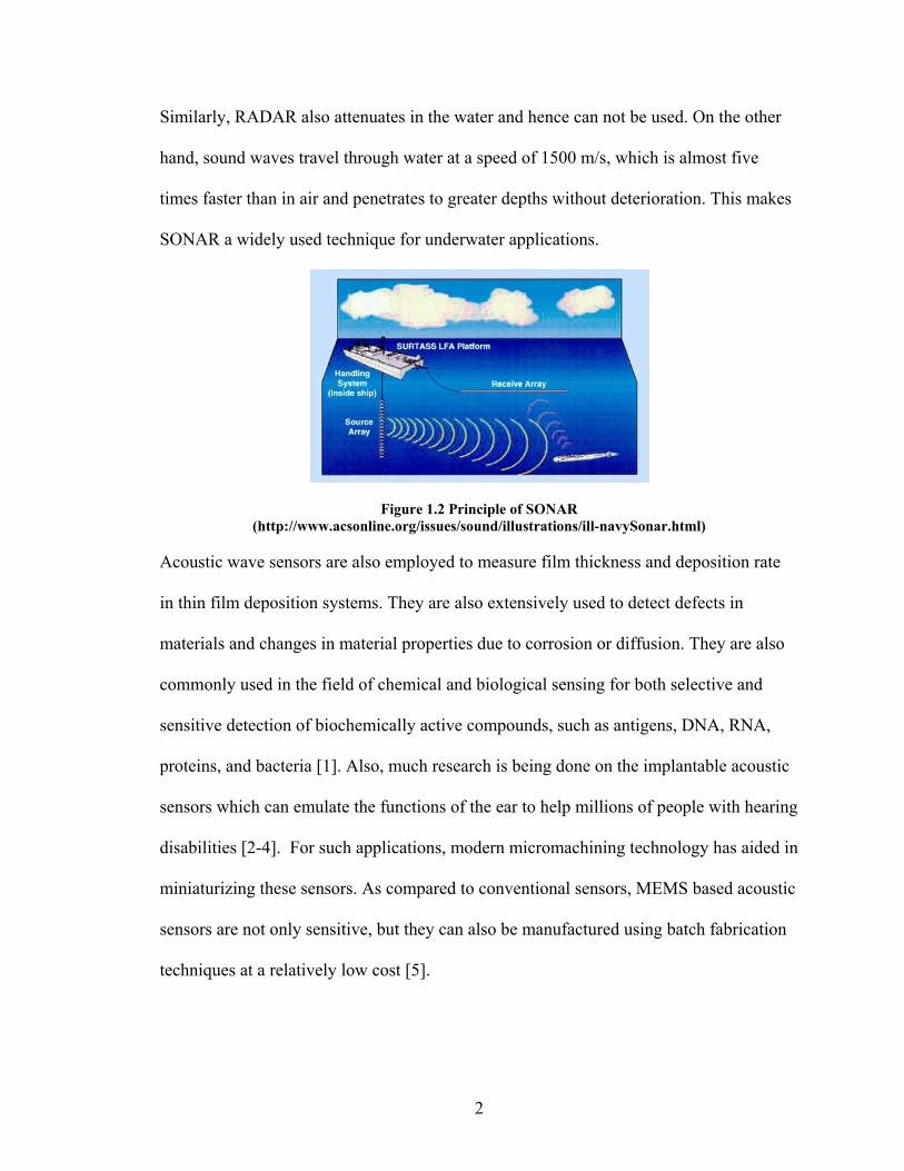
2
Similarly, RADAR also attenuates in the water and hence can not be used. On the other
hand, sound waves travel through water at a speed of 1500 m/s, which is almost five
times faster than in air and penetrates to greater depths without deterioration. This makes
SONAR a widely used technique for underwater applications.
Figure 1.2 Principle of SONAR (http://www.acsonline.org/issues/sound/illustrations/ill-navySonar.html)
Acoustic wave sensors are also employed to measure film thickness and deposition rate
in thin film deposition systems. They are also extensively used to detect defects in
materials and changes in material properties due to corrosion or diffusion. They are also
commonly used in the field of chemical and biological sensing for both selective and
sensitive detection of biochemically active compounds, such as antigens, DNA, RNA,
proteins, and bacteria [1]. Also, much research is being done on the implantable acoustic
sensors which can emulate the functions of the ear to help millions of people with hearing
disabilities [2-4]. For such applications, modern micromachining technology has aided in
miniaturizing these sensors. As compared to conventional sensors, MEMS based acoustic
sensors are not only sensitive, but they can also be manufactured using batch fabrication
techniques at a relatively low cost [5].

3
The goal of this thesis was to develop a nanowire-based acoustic sensor for underwater
applications. The design of the sensor was inspired by the structure, packaging, and
transduction mechanism of the human-ear cochlea. The sensor was fabricated using
micromachining techniques, incorporating nanowires that mimic stereocilia in the
human-ear cochlea [6]. The sensor has been designed to operate primarily for underwater
applications.
1.2. Ear: A natural acoustic sensor The human ear is a broadband acoustic sensor with a wide frequency range (20 Hz – 20
kHz). The human ear as a natural acoustic sensor has an incredible sensitivity in the
audible frequency range [7]. It can resolve about 1500 separate pitches with 16,000-
20,000 hair cells and can differentiate between sound waves whose frequencies differ by
as little as 1 Hz [8]. A brief overview of the human-ear structure and its operation is
given in the section 1.2.1. More detailed versions can be found in the literature [9-11].
1.2.1. Overview of cochlear biomechanics Structure: Figure 1.3 is a schematic of the structure of the human ear. The human ear can
be divided into three parts: the external ear comprising the pinna and the acoustic meatus.
It focuses sound vibrations to the tympanic membrane commonly called the ear drum, at
the beginning of the middle ear and aids in determining the location of an acoustic source.
The middle ear comprises three tiny bones collectively called auditory ossicles: the
malleus, the incus and the innermost bone called the stapes, which is in contact with the
oval window of the fluid chamber containing cochlear fluid. Its function is to transform
air-born vibrations impinging on the tympanic membrane into acoustic oscillations of the

4
fluid filling the cochlear duct of the inner ear. In other words, the middle ear bones act as
an impedance matching system between the environment and the cochlea. The inner ear
consists of two functional units: one is the vestibule and the semicircular canals
containing the sensory organs of postural equilibrium and the other is the cochlea, which
contains the sensory organ of hearing.
Figure 1.3 Structure of the human ear [9]
Figure 1.4 shows the schematic of the inner structure of the cochlea. The cochlea is a
spiral shaped organ consisting mainly of three ducts: scala tympani, scala media
(cochlear duct), and scala vestibuli, separated by Reissner’s membrane and the basilar
membrane respectively. The cochlear duct is filled with endolymph, while the scala
vestibuli and the scala tympani are filled with perilymph. They meet each other through
an opening at the apex of the cochlea, called the helicotrema. The basilar membrane in
the organ of Corti (Figure 1.5) of the cochlea has different acoustic impedances along its
length which enable it to spatially resolve different frequencies. While the higher
frequency acoustic waves excite the basilar membrane near the base of the cochlea, the
lower frequency waves excite it near the apex. The basilar membrane has sensory hair

5
cells on top of it. Each of these hair cells has hair-like stereocilia projecting from their
apical ends. When the stereocilia are deflected under the fixed tectorial membrane due to
the motion of the flexible basilar membrane, the hair cells are stimulated, which then
send nerve impulses via the vestibulocochlear nerve to the brain stem.
Figure 1.4 Structure of the Cochlea [9]
Figure 1.5 Structure of the organ of Corti [9]
Hearing: Figure 1.6 shows the schematic of how sound waves travel from air through the
ear and generate nerve impulses responsible for hearing. The acoustic waves enter the
outer ear and pass through the external auditory canal to reach the tympanic membrane.
This leads the tympanic membrane and the auditory ossicles to vibrate. This results in

6
stapes motion against the oval window and creates pressure waves in the perilymph of the
scala vestibuli of the cochlea. These waves are then transmitted across Reissner's
membrane into the endolymph of the cochlear duct. Vibrations in the scala vestibuli also
continue to travel around the apex of the cochlea through the helicotrema and transfer the
motion into the perilymph of the scala tympani. Higher frequencies do not propagate to
the helicotrema but are transmitted through the endolymph in the cochlea duct to the
perilymph in the scala tympani. As a result, the basilar membrane vibrates due to the
pressure difference across it. This results in an amplified response at a position along its
length where the impedance results in a resonant frequency corresponding to the
frequency of the incident wave. The motion of the basilar membrane deforms cilia on top
of it by shearing them against the fixed tectorial membrane resulting in the stimulation of
the hair-cells of the organ of Corti. These hair-cells then fire nerve impulses that travel
along the cochlear nerve (a branch of the auditory nerve) to the brain, where they are
interpreted as sound. In the meantime, the sound wave in the scala tympani causes the
round window to bulge outward and dampen the wave in the perilymph.
Figure 1.6 The mechanism of hearing [9]

7
1.3. Different types of acoustic sensors Many practical devices have been fabricated at the microscale to mimic the cochlear
function. Some of them are reported in this thesis as examples. Haronian and Macdonald
(1996) [12] proposed an array of silicon beams of gradually varying lengths to mimic the
basilar membrane. Their idea was to utilize the silicon beams of different resonant
frequencies to mechanically filter the acoustic input into discrete frequency bands and
produce corresponding electrical output signals that could be further used for speech
recognition, sound localization etc. The beams had a width of 1µm, height of 10 µm, and
lengths between 0.37 mm and 7 mm, with resonance frequencies between about 100 Hz
and 20 kHz. However, no kind of fluid coupling for transduction of sound waves existed
in their structure.
Ando et al. (1998) [13] described a fish-bone structure to make an artificial basilar
membrane microphone operated in air shown in Figure 1.7. The fishbone structure was
formed of 7 µm thick polysilicon beams of different lengths resting on a core backbone
of the same material. This backbone was used to transfer vibrations along the device to
the lateral beam resonators of individual frequencies, simulating the cochlea’s fluid
channel function. However, the input transverse beam unlike cochlear fluid was too stiff
to vibrate properly to the acoustic input signal.

8
Figure 1.7 Silicon micro-fishbone structure as artificial basilar membrane microphone [13]
Hemmert et al. (2003) [14] proposed a two duct fluid-filled MEMS-based mechanical
cochlea. A 3.5 cm long, 1-3 µm thick, and 1-2 mm wide membrane similar to the basilar
membrane was built using SU-8 polymer. Filtered water was used as the filler fluid. The
authors used the impulse response at two very closely spaced locations to demonstrate the
existence of a traveling wave and demonstrated up to 30π phase accumulation.
White and Grosh (2005) [15] reported on another two duct fluid filled MEMS cochlea
design with a tapered basilar membrane made of silicon nitride beams embedded in a
polymer. Silicon nitride was used for beams to reduce the residual stress in them. The
width of the beam array varied between 10 and 20 µm with beams spaced 2 to 4 µm
apart. The membrane had 32 capacitors spaced along its length to get the vibration of
individual beams in response to the different frequencies of sound ranging from 100 Hz
to 10 kHz.
Figure 1.8 Cross-sectional view of the device without the fluid [15]

9
Figure 1.9 Picture of the final device with the top electrode die bonded and wirebonded into a package. This device had been filled with silicone oil [15]
A few examples of micromachined microphones as well as hydrophones in the literature
are also listed here. These sensors are not biologically inspired and emphasis is paid to
the sensing mechanism and fabrication approach. Scheeper et al. (1993) [16] designed
and fabricated a microphone, which could operate up to the frequency of 20 kHz. Figure
1.10 shows the cross-sectional view of the microphone. The microphone consisted of two
wafers: a diaphragm and a backplate wafer joined together by gold-gold
thermocompression bonding. The diaphragm wafer consisted of a 1.95 mm diameter and
0.5 µm thick silicon nitride membrane coated with gold electrodes and the backplate
wafer consisted of the gold circuitry for capacitive sensing. The microphone required an
external power supply, since it was a condenser microphone. The sensitivity approached
-33 dB re 1 V/Pa for this microphone.

10
Figure 1.10 Cross-sectional view of the silicon nitride microphone by Scheeper et al. [16]
Bernstein et al. (1997) [17] fabricated a ferroelectric sonar transducer utilizing a MEMS
sol-gel PZT array to measure the vibration of a silicon membrane. The device (Figure
1.11) consisted of 8x8 arrays and was operated in water in the frequency range of 0.3 to 2
MHz. A 10 µm silicon membrane was formed by an anisotropic wet etching process
using EDP, on top of which PZT was patterned. The authors reported sensitivity of the
device reaching -235 dB re 1 V/µPa.
Figure 1.11 Cross-sectional view of the PZT hydrophone [17]

11
1.4. Proposed sensor As discussed earlier in section 1.3, it can be observed that a majority of existing acoustic
sensors, including cochlear-like sensors, are based on membrane deflection to detect
sound. However, typically in cochlea, both basilar and tectorial membranes are needed to
convert acoustic waves into mechanical stresses in stereocilia. Stresses in the cilia arise as
a result of their shearing against the more rigid tectorial membrane when the basilar
membrane deflects in response to acoustic pressure oscillation. It is the shearing of these
stereocilia that ultimately triggers biochemical reactions that cause hair-cells to send
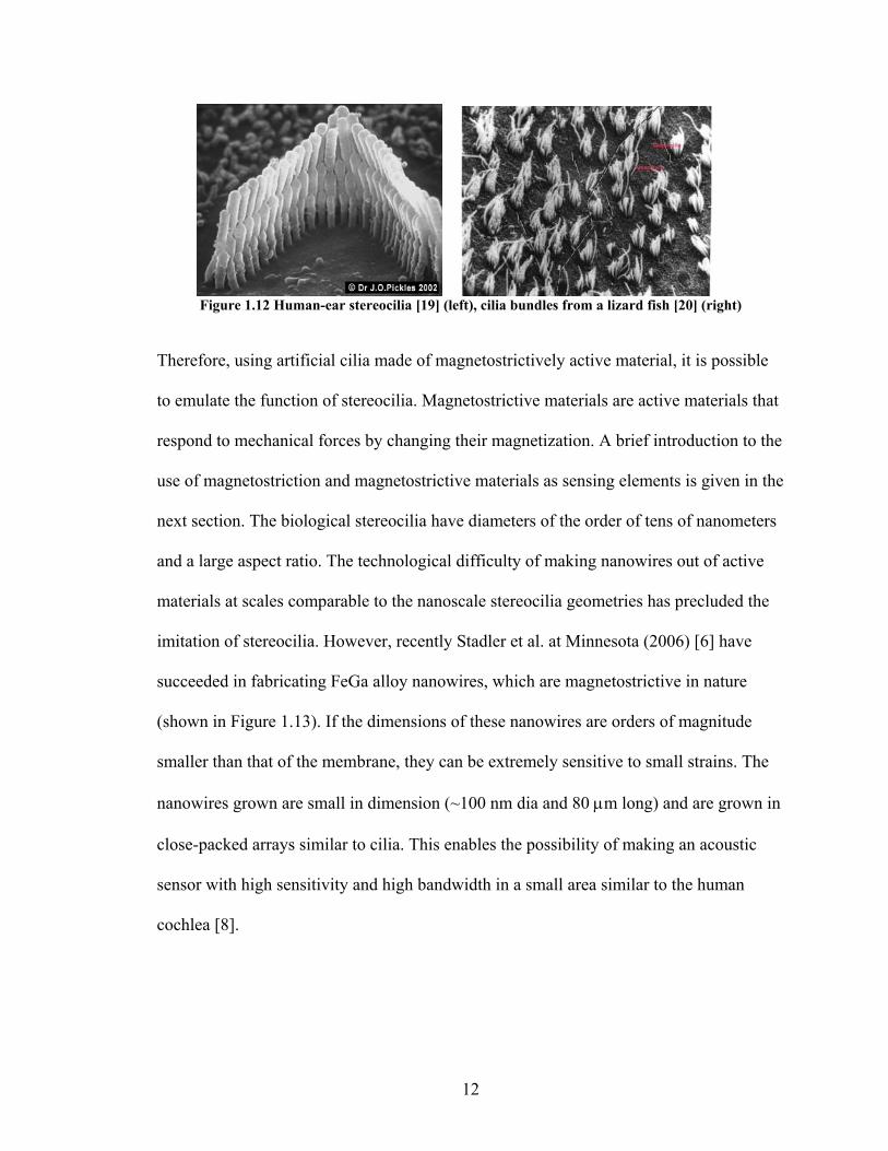
nerve impulses to brain. Figure 1.12 (left) shows the hair-like stereocilia present in
human-ear cochlea.
Also, cilia play an important role in the hearing mechanism of fish and other aquatic
animals. In fish, instead of a cochlea, they have a lateral line, a sense organ which helps
the fish to avoid collisions, locate prey, and orient itself in relation to water currents. The
lateral line is a collection of small mechanical receptors composed of a group of hair cells
called neuromasts located under the skin in fluid-filled canals on the body of all fish [18].
The hair cells are the same sensory cells found in the human-ear cochlea. The ciliary
bundles when stimulated by the sound waves activate the hair cells to transduce
mechanical energy into electrical energy. The electrical signals are carried to the brain
through nerves, which allows fish to perceive sound similar to the principle of hearing in
the human ear. Figure 1.12 (right) shows the cilia bundles from a lizard fish.
12
Figure 1.12 Human-ear stereocilia [19] (left), cilia bundles from a lizard fish [20] (right)
Therefore, using artificial cilia made of magnetostrictively active material, it is possible
to emulate the function of stereocilia. Magnetostrictive materials are active materials that
respond to mechanical forces by changing their magnetization. A brief introduction to the
use of magnetostriction and magnetostrictive materials as sensing elements is given in the
next section. The biological stereocilia have diameters of the order of tens of nanometers
and a large aspect ratio. The technological difficulty of making nanowires out of active
materials at scales comparable to the nanoscale stereocilia geometries has precluded the
imitation of stereocilia. However, recently Stadler et al. at Minnesota (2006) [6] have
succeeded in fabricating FeGa alloy nanowires, which are magnetostrictive in nature
(shown in Figure 1.13). If the dimensions of these nanowires are orders of magnitude
smaller than that of the membrane, they can be extremely sensitive to small strains. The
nanowires grown are small in dimension (~100 nm dia and 80 μm long) and are grown in
close-packed arrays similar to cilia. This enables the possibility of making an acoustic
sensor with high sensitivity and high bandwidth in a small area similar to the human
cochlea [8].

13
Figure 1.13 FeGa (Galfenol) nanowires
The proposed nanowire acoustic sensor was motivated by the architecture of the human-
ear cochlea. It is a micromachined device consisting of an elongated cavity with two fluid
channels and a flexible membrane partition between them, playing the role of the basilar
membrane. The nanowires made of FeGa are to be attached to this flexible membrane on
one side and in contact with the fixed membrane on the other side. As described above,
the nanowires are used to mimic the functionality of the stereocilia and the fixed
membrane is used to emulate the tectorial membrane. The nanowires respond to the
external forces by changing their magnetization, and a magnetic sensor is used to
measure these changes.
Fabrication was the major challenge associated with building this cochlear-like sensor.
Since it is a microscale device, micromachining techniques were employed. Since the
sensor has been primarily designed for underwater applications, its packaging is also
more challenging than that of microelectromechanical devices used in ambient
environments. The inspiration for the external package design of the sensor was also
derived from the structure and the transduction mechanism of the cochlea and the

14
structure of the hearing organ of the fish. The tissues composing the body of the fish have
the same acoustic impedance as that of the water. This allows sound to pass through them
with minimum attenuation and interact with the lateral line in which the ciliary bundles
(analogous to cilia on hair cells in the basilar membrane in the cochlea) are found inside
the fish body [21]. In the human ear, middle ear bones ensure impedance match between
the low impedance acoustic oscillations in the tympanic membrane and the high
impedance fluid in the cochlear duct. Inspired from them, the package was designed to
include an acoustically transparent window minimizing the attenuation of sound passing
through it. For this, the material and fluid medium must be selected such that their
acoustic impedance matches closely to that of sea water in order to minimize the
reflection of incoming sound waves at material interfaces. For this purpose, the acoustic
performance of different package materials filled with fluids has been investigated. These
studies were conducted in water and quantified package and fluid impedance and
attenuation characteristics and moisture absorption properties.
1.5. Background on Magnetostriction Magnetostrictive materials are a special subset of ferromagnetic materials, which can be
broadly defined as materials that undergo a change in physical dimensions when
subjected to a magnetic field and conversely, undergo a change in their magnetization
when subjected to an externally applied stress. The effect was first identified in 1842 by
James Joule. The internal crystal structure of the magnetostrictive material is divided into
domains, each of which is a region of uniform magnetic polarization. In the absence of a
magnetic field or stress, the series of domains have randomly oriented magnetic moments.
When a magnetic field is applied, the boundaries between the domains (domain walls)

15
shift, rotating the domain. Due to the realignment of magnetic domains in the direction of
the field, there is a change in the material's length Δl called magnetostriction, and a
change in the magnetic induction B of the sample. Magnetostrictive materials induce
strain irrespective of the polarity of applied magnetic field. This is known as Joule’s
effect and is used for actuation purposes.
Figure 1.14 The rotation and movement of magnetic domains causes a physical length change in the material (Joule’s effect). (b) Independence of strain on polarity of applied field [22].
It is a common practice to apply compressive pre-stress on the magnetostrictive material
if used for actuation purposes, which can be easily explained using Figure 1.15. When
there is a maximum compressive pre-stress applied, the domains become normal to the
direction of the applied stress and as the field is increased, these domains realign parallel
to the direction of the applied stress and thus maximum magnetostriction, λmax can be
achieved. Figure 1.16 shows a set of magnetostriction versus magnetic field curves (or λ-
H curves) at various levels of mechanical pre-stress. The corresponding positions A, B,
and C from Figure 1.15 can be seen on the graph in Figure 1.16. Point C indicates the
saturation state.

16
H=0
A C
σ
bias
B
λmax
H=0
A C
σ
biasσ
bias
B
λmax
Figure 1.15 Schematic illustrating actuation behavior in magnetostrictive materials (Joule’s effect) with the help of rotation of magnets [23]
Figure 1.16 Actuator characterization curves of Magnetostriction vs Magnetic field for 18.4% gallium Galfenol for various stress levels [22]
Conversely, the magnetic flux density of the material changes when subjected to a
mechanical stress. This is called the Villari effect. The Villari effect is used for sensing
applications. A biased magnetic field is usually applied to the magnetostrictive material
to maximize the change in the magnetic flux density ΔB in response to a given stress
application. This is because the bias field aligns the domains parallel to the direction of
the field resulting in a net magnetization along that direction. When a compressive stress
is applied, the domains re-orient, changing the net magnetization resulting in magnetic
flux density change, ΔB. This is illustrated in Figure 1.17 and Figure 1.18 . It should be
A
B
C

17
noted that in the absence of a biased magnetic field there will not be any initial
magnetization and hence the resulting change in the magnetic flux density due to the
application of stress will be zero.
σ = 0
Hbias
ΔBmax
σ = 0
Hbias
Hbias
ΔBmax
Figure 1.17 Schematic illustrating sensing behavior in magnetostrictive materials with the help of rotation of magnets. The stress applied to a magnetostrictive material changes its magnetic flux
density (Villari effect) [23]
Figure 1.18 Magneto-mechanical sensor characterization curves of a 19% gallium Galfenol [24]
The most common unit systems to define magnetic quantities are either Gaussian /CGS
system or SI system. The table below shows the units and conversion factors for common
magnetic quantities for reference purposes.

18
Table 1-1 Unit system and conversion factors for magnetic quantities Quantity CGS units Conversion factor
CGS ---> SI SI units
Magnetic field strength (H) Oersted (Oe) 79.58 A/m Magnetic flux density (B) Gauss (G) 1 x 10⁻⁴ Tesla (T) Magnetization (M) emu/cc 1 x 10³ A/m Magnetic flux (φ) Maxwell (Mx) 1 x 10⁻⁸ Weber (Wb) Magnetic permeability (µ) Dimensionless 4π x 10-7 H/m
1.5.1. Magnetostrictive materials Nickel and iron are the materials in which magnetostriction was first observed (45 ppm
for nickel, 15 ppm for iron) [22]. Since then, alloys of iron have been discovered that
exhibit a “giant” magnetostrictive effect under relatively small fields. Terfenol-D, a
specially formulated alloy of Terbium, Dysprosium, and Iron is a very popular giant
magnetostrictive material that exhibits a large magnetostriction of 2000 ppm in a field of
2 kOe at room temperature. However, it is brittle, with an ultimate tensile strength of 28
MPa, limiting its application only to uniaxial stresses [25]. Therefore, other alternative
materials are being investigated, which not only show high magnetostriction but are
ductile and machinable.
Galfenol One magnetostrictive material under current investigation is an iron-gallium alloy (Fe1-
xGax) termed Galfenol which appears to be a promising material for a variety of actuator
and sensing applications. It exhibits magnetostriction peaks (~350-400 ppm) at 19 and 27
atomic % gallium at low applied magnetic fields (~100 Oe) and has very low hysteresis
[26]. Figure 1.19 shows saturation magnetostriction values measured for different
stoichiometries of single crystal Galfenol with 10 to 35 atomic % gallium content. In

19
addition to these unique magnetostrictive properties, Galfenol has good mechanical
properties and can be machined. Galfenol’s elastic modulus, permeability, and
piezomagnetic coefficients are quite constant over temperatures ranging from -20°C to
+80°C [26] and it demonstrates high tensile strength (~500 MPa), good machinability,
and good ductility [27, 28]. In addition to the transduction properties of Fe-Ga alloys,
their ability to withstand shock loads and harsh operating environments, and to operate in
both tension and compression, and hence in bending, makes them suitable for a variety of
sensors and actuators including those at the micro and nanoscales [29].
0 5 10 15 20 25 30 35 40
0
50
100
150
200
250
300
350
400
450
3/2
λ 100
(x 1
0-6)
x
Furnace Cooled Quenched Directionally Solidified (Unannealed) Quenched in Brine Furnace Cooled, Multi-phase
Fe100-xGax
H = 15 kOe
Figure 1.19 Magnetostriction versus Gallium content in single crystal Galfenol [26]
Magnetostrictive materials are often used as transducers in acoustic underwater systems
for geophysical surveying and exploration, ocean tomography, mine clearance,
underwater information exchange, and underwater sonar systems. They are also used as
broadband vibration sources in speakers, as well as in laboratory and industrial shakers.
Ultrasonic, high-frequency, high-power magnetostrictive actuators are used in medical,
dental, petrochemical, and sonochemical applications [22]. Sensor systems, such as force,

20
moment and torque meters, based on magnetostrictive transduction are also under use
[23].
Both piezo-electric and magnetostrictive materials demonstrate very high bandwidth
(~100 KHz) making them well suited to high frequency applications such as vibration
control and SONAR. However, piezo-electric materials require very large electric fields
(~5 kV/cm) and may suffer from self-heating problems. On the contrary,
magnetostrictive FeGa alloys posseses some promising properties, such as high tensile
strength (20 times that of typical piezo-electric), lower bias field for actuation, and the
ability to withstand underwater shocks and explosions. These characteristics may enable
the use of these alloys as compact actuators and sensors in harsh and shock prone
environments. In addition, the ability to use small permanent magnets with low hysteresis
limits self-heating, making them potentially better choices for these applications than
piezo-electrics. This is also a direct application of magnetostrictive actuation without any
necessity for stroke amplification and has been very popular with the Navy [23].
1.5.2. Nanowire Fabrication As discussed in section 1.4, Galfenol nanowires in an acoustic sensor mimic the action of
hair-like stereocilia present in human ear and other biological species [6]. Since bending
of these naowires results in simultaneous compression and tension, the net magnetization
change in the nanowire would average to zero if the alloy was uniformly isotropic and the
trends in magnetization change due to tension and compression were similar. However,
the change in the magnetization of a FeGa alloy in compression is significantly larger
than in tension. Therefore, during bending, the response of the galfenol nanowire is

21
dominated by the compression. This has been demonstrated at the bulk level by Downey
et al. [29]. Hence, FeGa nanowires are ideal for artificial cilia applications. Their other
potential applications are in fluid flow sensing and detection of chemical contamination
[30].
The Galfenol nanowires being grown at the University of Minnesota are 20-200 nm in
diameter and about 25-100 µm in length. Figure 1.20 shows the nanowire fabrication
process [30-32]. The fabrication procedure for making nanowires starts with
electropolishing and first anodization of aluminum, thus creating a porous template.
These pores are not straight and uniform and hence this disordered alumina is etched
away with 1.8 wt% chromic and 6 wt% phosphoric acid for 20 min, leaving small
dimples at the aluminum surface. A second anodization is done which creates ordered
pores with uniform diameters and spacing. The remaining aluminum is etched away from
the back side along with the barrier layer with saturated HgCl2 (mercuric chloride)
solution leaving straight through holes in the template. A copper electrode is then
sputtered on the back of the template and FeGa alloy is electrochemically deposited into
the pores. Later, the alumina template is etched back exposing the nanowires.

22
Figure 1.20 The nanowire fabrication process [30]
As discussed in section 1.5, it is important to bias FeGa to use it as a sensor. For this
purpose, research is underway to grow the nanowires with an initial cobalt layer that can
act as a bias layer. Also, as discussed in section 1.4, a magnetic sensor must be used to
measure the change in the magnetization of these nanowires in response to the motion of
the flexible membrane. However, even the smallest sensing area of a commercially
available magnetic sensor (~ 50 μm x 50 μm for GMR – giant magnetoresistive sensor
made by NVE Volatile Inc.) is significantly larger than the nanowire diameter. Also, the
whole GMR sensor is about 4.5 mm x 3 mm in size, which makes it extremely difficult to
use with the micromachined nanowire acoustic sensor. Therefore, attempts to grow
nanowires with the magnetic bias layer (Co), active layer (FeGa) and GMR layer (Cu/Co)
all integrated are underway to completely eliminate the need for a commercial GMR
sensor [33]. With the GMR sensor integrated within the nanowire, it would be possible to
measure the response of each individual nanowire. However, in the work presented in
this thesis, the sensor was designed to be used with a commercial GMR sensor.

23
Figure 1.21 Nanowires coupled with Co bias layer and multi-layered GMR sensor [30]
1.6. Organization of this thesis The organization of this thesis and contributions towards the design, fabrication, and
preliminary testing of the iron-gallium nanowire based acoustic sensor is summarized
below:
Chapter 2: DESIGN – Analogy to Human-Ear Cochlea
This chapter discusses the iron-gallium nanowire acoustic sensor structure and operation
as an analogy to the human-ear cochlea. It includes the challenges related to the
identification of the key components of the sensor and their respective material selection.
There are three main components responsible for the effective operation of the sensor –
magnetic flux path, membrane structures (playing the role of the basilar and tectorial
membrane), and external packaging. Packaging plays an important role as the sensor is
mainly meant for use in underwater applications.

24
Chapter 3: Process Sequence for Fabricating the Sensor
The micromachining processes and techniques and the process sequence used for the
fabrication of the nanowire based acoustic sensor are discussed in detail. This chapter
also includes the limitations and challenges encountered while using these
micromachining techniques for the fabrication of such a miniaturized sensor. Design
efforts and solutions for developing this acoustic transducer have been described in this
chapter.
Chapter 4: Experimental Testing
This chapter focuses on the test setup and procedure for testing the three key components
of the sensor. The first set of experiments tested the response of the device membrane in
air using a Laser Vibrometer. The second experiment involved qualitative magnetic force
microscopy (MFM) testing of a nickel thin film used as a magnetic flux path. The third
experiment was the acoustic testing of the candidate encapsulants and filler fluids. Lastly,
an experiment was performed to test the response of the packaged device in water. The
preliminary testing of the device was done without nanowires as they were not available
at that time. The chapter includes the results and inferences obtained from those
experiments and also discusses the limitations in the measurement techniques and
equipment.
Chapter 5: Conclusions and Contributions
This chapter summarizes the steps involved in the development of the nanowire based
acoustic sensor and the significant contributions made in the work.

25
2. DESIGN – ANALOGY TO HUMAN-EAR COCHLEA Many aspects of the transduction mechanism, design, and packaging of the iron-gallium
nanowire acoustic sensor are analogous to (and are inspired from) those found in the
human-ear cochlea. Figure 2.1 and Figure 2.2 are drawings of the cross-sectional view of
an uncurled human-ear cochlea and the iron-gallium nanowire acoustic sensor,
respectively. The figures indicate the analogy between the biological human-ear cochlea
and its mechanical counterpart – the nanowire acoustic sensor. It can be observed that in
the cochlea there are two fluid channels separated by the basilar membrane. The oval
window and the round window are flexible membranes at one end of the upper and lower
channels, respectively. The oval window facilitates transfer of acoustic pressure
oscillating into the cochlea. The round window facilitates pressure equalization and helps
damp out acoustic oscillations in the chamber. Connecting these two channels is
helicotrema which allows the sound waves to travel from the top to the bottom channel
thereby doubling the pressure difference across the basilar membrane and hence
amplifying its motion. Analogous to this, the nanowire acoustic sensor consists of two
fluid channels with a window on one side of both the channels. While the acoustically
transparent window that allows sound waves to reach the sensor is analogous to the oval
window, the other window that damps the sound waves is analogous to the round window.
An opening on the other side, connecting the two channels, is similar to the helicotrema.
There are two membranes in the cochlea. The one separating the two channels is the
basilar membrane, which moves in response to the sound waves and has stereocilia on
top of it. The other one is the fixed tectorial membrane against which stereocilia shear
when the basilar membrane moves/vibrates. The flexible and fixed membranes in the

26
mechanical sensor play the roles of basilar and tectorial membranes respectively. The
nanowires (often referred to as artificial cilia) in the mechanical sensor not only
dimensionally but also functionally mimic the stereocilia.
A difference in impedances (or impedance mismatch) of two media results in the reduced
sound transmission. The tympanic membrane and the ossicles in the middle ear function
to overcome the mismatch of impedances between air and the cochlear fluids and thus
reduce the resistance to the sound passage. Similarly, the challenge involved in the
nanowire acoustic sensor is to minimize the difference in impedance between sea water
and filler fluid thus minimizing the transmission loss before the sound reaches the
sensing element. The use of acoustically transparent materials and filler fluids in the
sensor allows the sound waves to pass with little attenuation. Mechanical amplification as
is accomplished in the middle ear is not addressed in the current design considerations,
but is encouraged as a consideration for future impedance matching concepts.
Hair cell sectionOval
Window
Fluid at rest
Basilar membrane
Round window
Stapes Fluid circulation through helicotrema
Hair cell sectionOval
Window
Fluid at rest
Basilar membrane
Round window
Stapes Fluid circulation through helicotrema
Cilia
Hair cell sectionOval
Window
Fluid at rest
Basilar membrane
Round window
Stapes Fluid circulation through helicotrema
Hair cell sectionOval
Window
Fluid at rest
Basilar membrane
Round window
Stapes Fluid circulation through helicotrema
CiliaCilia
Tectorial membrane
Hair cell sectionOval
Window
Fluid at rest
Basilar membrane
Round window
Stapes Fluid circulation through helicotrema
Hair cell sectionOval
Window
Fluid at rest
Basilar membrane
Round window
Stapes Fluid circulation through helicotrema
Cilia
Hair cell sectionOval
Window
Fluid at rest
Basilar membrane
Round window
Stapes Fluid circulation through helicotrema
Hair cell sectionOval
Window
Fluid at rest
Basilar membrane
Round window
Stapes Fluid circulation through helicotrema
CiliaCilia
Tectorial membrane
Figure 2.1 Schematic of the cross-section of the human-ear cochlea (http://www.vimm.it/cochlea/cochleapages/theory/hydro/hydro.htm)

27
Tectorial Membrane: Pyrex
Basilar Membrane: Silicon
Nanowires
PDMS
Silicone oilNickelSoundwaves
Sound inlet: oval window
Sound outlet: round window
(a)
(b)
Figure 2.2 Schematic of the (a) front, (b) side cross-section of the iron-gallium nanowire acoustic sensor
Based on the physiology and transduction process of the human-ear cochlea, the acoustic
sensor includes a fluid cavity corresponding to the fluid-filled cochlea. The cavity
consists of a flexible membrane similar to the basilar membrane in the cochlea, which
vibrates in response to sound waves. At the top of the flexible membrane, Galfenol
nanowires analogous to stereocilia are attached. Another membrane fixed in nature and
functionally similar to the tectorial membrane lies above and touches the free end of the
Galfenol nanowires. On interaction with the sound waves, fluid in the cochlea sets in
motion and vibrates the basilar membrane, shearing cilia against the tectorial membrane.
The sheared cilia trigger the hair-cells to fire an electrical signal. Similarly, in the

28
acoustic sensor, the flexible membrane vibrates because of fluid action in response to
sound waves, displacing the nanowires and shearing them against the fixed membrane.
The bending of the magnetostrictive nanowires causes a stress induced change in the
magnetic flux density that could be measured by a magnetic sensor that provides a
corresponding electrical output. It should be noted that there is a difference in the sensing
mechanisms of the ear and the mechanical sensor. Electrochemical reactions triggered in
the hair cells by the moving cilia generate nerve impulses in the ear. However, in the
proposed mechanical device, a magnetic sensor gives a voltage output proportional to the
stress induced change in the magnetic flux density of the nanowires.
2.1. Design and Operation
Device Structure The iron-gallium nanowire acoustic sensor is a MEMS scale and a bio-inspired sensor
that is analogous to the human-ear cochlea. The manufacturing and packaging of the
acoustic sensor is done using micromachining techniques at the wafer level, which is not
only cost-effective but also allows fragile, contamination-sensitive nanowires to be
protected in the ultra-clean environment of the fab. Figure 2.3 and Figure 2.4 show the
three-dimensional view of the cochlea and the acoustic sensor, respectively.
The nanowire acoustic sensor consists of a square flexible membrane of silicon fabricated
with the help of photolithographic techniques on top of which is attached the nanowire
substrate. The dimensions of the membrane were chosen from 1 mm x 1 mm to 3 mm x 3
mm depending on the size of the substrate of nanowires available from Prof. Stadler at

29
the University of Minnesota. The membrane is fixed from two sides and separates the
fluid cavity into two parts similar to the basilar membrane as explained in the previous
section. Use of a low viscosity liquid medium inside the package was preferred in order
to reduce viscous damping of the nanowire motion. The liquid also transports the acoustic
pressure waves coming from the oval window (acoustically transparent window) to the
flexible membrane and hence it must be close in acoustic impedance to the window
material and the sea water to minimize sound reflection. The channel below the
membrane has two open ends; one of them is encapsulated with an acoustic impedance
matching material to allow the sound waves to enter through the package with minimal
attenuation. These sound waves interact with the impedance matched fluid inside the
channels to vibrate the membrane. The other end of the bottom channel connects to the
top channel allowing the flow of sound waves through the fluid. This results in
effectively doubling the pressure difference across the membrane, which results in its
greater displacement. One of the ends of the top channel acts similar to the round window
in the cochlea damping out the sound waves without creating any reflections and echoes
within the sensor cavity. For this purpose, the window must be filled with a material of
low impedance compared to the fluid in the chamber. This can be ensured by introducing
air pockets in the encapsulation material, which will diffuse the acoustic oscillations.
However, in the current design use of such low impedance material has not been
addressed. Nevertheless its use in future designs is recommended. The nanowires were
glued on the flexible membrane with a thin film of photoresist (SU-8). It is difficult to
estimate the thickness of this film of photoresist, which is one of the reasons why it is
encouraged that nanowires be grown directly on nanowires is encouraged to be

30
integrated with the membrane surface in the future design. A fixed membrane (similar to
the tectorial membrane) of either pyrex or silicon is bonded along with the flexible
membrane to a spacer silicon wafer of thickness equal to the length of the nanowires.
This will ensure the nanowires attached to the flexible membrane are in contact with the
fixed membrane at their free end. This is important because it is the bending or shearing
of these nanowires as a result of the wiggling of the flexible membrane in response to the
sound waves that results in a change in the magnetic flux density. The bonding between
the two membranes was achieved by cold welding of pure indium solder at room
temperature creating a hermetic joint.
A commercially available GMR sensor attached to the acoustic sensor measures the
change in the magnetic field due to the bending of nanowires and gives an electrical
output. However, the GMR sensor available was 15 mm x 4 mm in dimension and
therefore, could not be placed in the same fluid cavity as the nanowires. A preliminary
finite element model of the nanowires done by Mudivarthi [34] showed that the GMR
sensor should be placed as close to the nanowires as possible to detect the minute
changes in magnetic flux density resulting from their pressure induced bending. To
permit the GMR sensor to be remotely located while still receiving detectable levels of
magnetic flux density required the deposition of a thin film of material with good
magnetic properties to serve as a closed magnetic flux path between the nanowires and
the GMR sensor. The pressure induced bending of nanowires results in magnetic state
changes which are carried along a flux path to the GMR sensor without significant losses.
Ongoing research to integrate the GMR sensor with the base of the iron-gallium

31
nanowires is being conducted by Prof. Stadler at University of Minnesota as discussed in
section 1.5.2. This would eliminate the use of the large commercially available GMR
sensor and thus help in further miniaturizing the sensor.
Figure 2.3 Representation of the 3-D view of uncoiled biological cochlea [35]
Fixed membrane NanowiresNickel
Acoustic waves
Flexible membraneGMR
PDMS
Silicone oil
Figure 2.4 Schematic of a 3-D view of the Galfenol nanowire acoustic sensor
Device Operation A description of the operation of the device (i.e. how acoustic waves in the ambient
underwater environment are converted to electrical signals by the device) is presented
next. When an acoustic pressure wave impinges on the acoustically transparent window,
part of the wave is reflected and the remaining part is transmitted through the window to

32
the filler liquid inside the sensor. The fraction of the reflected or transmitted acoustic
waves depends on how well matched the impedances of the encapsulation material and
the filler fluid are to the sea water. The closer the impedance of the window and fluid are
to the impedance of sea water, the more acoustically transparent they are to the pressure
wave. The encapsulation material and filler fluid were chosen to maximize energy
transmission to the filler fluid.
As a result of the incoming acoustic waves, the flexible membrane in contact with the
fluid begins to vibrate. The fluid medium inside the closed cavity can result in additional
impedance when it cannot move freely during the vibration. The opening provided at the
end of the channel helps to alleviate this problem by maintaining pressure balance at both
sides of the vibrating membrane similar to helicotrema in the cochlea. In addition, it helps
in doubling the pressure difference across the flexible membrane for greater displacement
of the membrane. Due to this displacement of the flexible membrane, fine nanowires that
are cantilevered normal to the plane of the membrane get sheared back and forth relative
to where the opposite end of the nanowire is pressed against the fixed membrane. The
shearing stress induces change in the magnetic flux density proportional to the bending of
these magnetostrictive iron-gallium nanowires. A magnetic flux path connects the flux
lines from the nanowires to where they can be sensed by a commercially available GMR
sensor to give an electrical voltage output that is proportional to the original acoustic
pressure wave.

33
2.1.1. Key components of the sensor
The structural design of the nanowire acoustic sensor consists of three important
components, which are critical for effective operation. Proper material selection and
testing for all the components is essential before they can be incorporated in the sensor.
This is explained in detail in sections 2.1.1.1- 2.1.1.3.
2.1.1.1. Flexible and fixed membrane: Basilar and Tectorial membrane The flexible membrane in the sensor is functionally similar to the basilar membrane. It is
square shaped, supported on two sides and vibrates as a result of interaction with the
sound waves. The purpose of the flexible membrane is to amplify the vibration of the
nanowires in response to the acoustic waves by virtue of its greater surface area. Early
FEA predictions of the vibration of Galfenol nanowires immersed in a fluid medium [34],
indicated that nanowires attached to a rigid surface would not respond sufficiently to the
acoustic waves to produce a measurable change in the magnetic flux density. Being
nanoscale in dimension, the pressure difference across these nanowires is too small to
deflect them appreciably. When these nanowires are attached to a membrane of greater
surface area, the higher force on the membrane surface leads to its larger deflection. The
larger deflection of the flexible membrane leads to the larger shearing of the nanowires
under the fixed membrane, consequently producing greater change in the magnetic flux
density.

34
2.1.1.1.1. Material selection The membrane is a critical part of the nanowire acoustic sensor. It should not only be
flexible but also be able to withstand the dynamic mechanical loads due to the acoustic
pressure waves. The common materials used for making MEMS membranes are silicon
nitride and silicon oxide thin films. The stoichiometric low pressure chemical-vapor
deposition (LPCVD) nitride thin film has a tensile stress of over 550.75 MPa and 0.3 µm
of an oxide film has a compressive stress about 429.49 MPa [36]. If the thin film of the
membrane is deposited with a resulting high compressive residual stress, the released
membrane will buckle and collapse [37]. On the other hand, high tensile residual stress
renders the membrane mechanically very stiff, resulting in possible rupture [37].
Therefore, a composite laminate membrane of alternating nitride and oxide films can be
made in which the tensile stresses due to the nitride and the compressive stresses due to
the oxide balance each other and result in lower net residual stress.
Table 2-1 Estimated residual stress and Young’s modulus [15]
Materials Residual Stress (MPa) Young’s Modulus (GPa)
Silicon Oxide -429.49 54.59
Silicon Nitride 550.75 270.54
It is difficult to fabricate thick (> 5 μm) composite membranes of silicon nitride and
silicon oxide. Pin-holes defects are generally formed while depositing thicker layers,
which degrade the membrane properties and operation. Thus, instead of making a
composite membrane, silicon was explored as a potential membrane material. Silicon
wafers used in the micromachining process are almost defect-free and do not have any
residual stresses. Silicon can also be reduced to any desired thickness by standard

35
micromachining processes, which is important to tune the dynamic properties of the
membrane.
Finite element modeling
A finite element model developed using Comsol Multiphysics™ 3.3 was used to
determine resonant frequency of membranes of different materials and dimensions.
Mindlin plate theory was used for the eigen-frequency analysis of a clamped-free-
clamped-free square membrane. This analysis allows the dimensions of the membrane for
different materials to be selected to have a desired resonant frequency. The magnitude of
the response of the membrane should be linearly dependent on the pressure of the
acoustic wave and hence it is desirable that its operation range be well below its resonant
frequency. If the membrane operates near the resonance even the slightest pressure wave
could lead to a large response thus making it difficult to know the pressure of the incident
acoustic wave. Table 2-2 shows the response of different membrane materials versus
different sizes of the membrane.
Table 2-2 Estimated eigen-frequency with membrane dimensions
Eigen frequency (Hz) for different membrane materials
Thickness
Membrane dimensions (mm x mm)
Silicon Nitride
2000 Ǻ
Silicon Oxide
1 µm
Silicon oxide
2 µm
Silicon
26 µm
1 x 1 1890 5874 11746 208100
2 x 2 472 1468 2937 52300

36
3 x 3 210 653 1303 20300
5 x 5 75 235 470 8360
10 x 10 28 58 117 2090
From the table it could be inferred that the membrane with smaller thickness should be as
small as possible in size to have a higher resonant frequency. However the membrane
dimensions were chosen to be 1x1 mm2, 2x2 mm2, or 3x3 mm2 based on the constraint of
the currently available nanowire substrate dimensions (2 – 10 mm2). Therefore, a
membrane with greater thickness was selected for proof of concept prototype
development in order to achieve higher resonant frequency.
2.1.1.2. Magnetic Flux Path The magnetic flux path between the nanowires and the GMR sensor serves as a bridge for
the flow of the magnetic flux lines. It increases the sensitivity of the device by directing
the magnetic flux lines to the GMR sensor when the nanowires bend. Various metals and
alloys have been investigated that can serve as a good magnetic flux path. The ideal
material would be one which has a high magnetic permeability to transmit the magnetic
flux lines with minimal losses. Another consideration was to maintain all the magnetic
flux lines in plane and parallel to the sensing axis of the GMR chip (explained in detail in
section 2.1.1.2.1).This is because the out of plane moments lead to flux leakage. As thin
films possess predominantly in-plane moments rather than out of plane moments due to
shape anisotropy, a thin film of the chosen material was deposited to connect the
nanowires and the GMR sensor [38]. Both elliptical and ring shapes were considered for

37
the flux path to avoid sharp corners which might increase the leakage of the magnetic
flux due to excessive flux concentration [38].
2.1.1.2.1. GMR Sensor A giant magnetoresistive sensor (GMR) is a magnetic sensor that exhibits a large change
in resistance in response to a magnetic field. It is a multilayer device having two or more
ferromagnetic layers separated by a nonmagnetic material layer. Electrical resistance of
the multilayer changes depending on the orientations of the magnetizations of the
ferromagnetic layers. The physics behind the GMR phenomena is based on the spin-
dependent scattering of the conduction electrons. The resistance is minimal when the
direction of the magnetic moments of the layers is parallel because the possibility of
electron scattering at the interface of conductor/ferromagnetic layers becomes smaller.
However, if the directions of the magnetizations of the two ferromagnetic layers are
opposite, the electron with opposite spin orientation with respect to the magnetization of
the electrode layer is scattered, resulting in higher electrical resistance [39, 40]. The
characteristic value usually associated with the GMR effect is the percent change in
resistance normalized by the saturated or minimum resistance. In those terms, various
commercial GMR sensors can achieve a change in resistance as large as 10% – 20% [41].
Due to this large change in resistance in response to the magnetic field, this phenomenon
is called giant magnetoresistance. GMR sensors are commonly being used as magnetic
read heads in magnetic data-storage media like hard discs because they help in reducing
the read access time [42]. A Wheatstone bridge is integrated in the GMR chip, which is

38
well suited for the measurement of small changes in its resistance when the magnetic
field changes.
I+
GND
Out-
Out+
I+
GND
Out-
Out+
Figure 2.5 GMR “Guitar” chip on a PCB, SEM of the GMR “Guitar” chip, and the wheatstone bridge at the bottom (Pictures courtesy Patrick Downey [43])
As discussed in section 2.1, Device Structure, a commercially available GMR “Guitar”
sensor (shown in Figure 2.5), has been attached to the nanowire acoustic sensor to
convert the change in the magnetic field due to bending of the nanowires to an electrical
output. The GMR “Guitar” sensor chip currently available from NVE Inc., Eden Prairie,
Minnesota is 15 mm x 4 mm in dimension and was wire bonded to a printed circuit board
Sensing direction
15 mm
4 mm

39
(PCB) in the shape of a guitar by the manufacturer. The sensing axis is along the width of
the GMR sensor chip, according to the data sheet provided. Due to the limitation of the
large size of the GMR chip, it was not possible to place it into the same cavity as the
nanowires. It was therefore placed outside the packaging cavity and connected to the
nanowires through the magnetic flux path.
2.1.1.2.2. Material selection Various potential elements and alloys which possess high magnetic permeability were
considered for the magnetic flux path, including Nickel, Permalloy: 78% Ni-Fe,
Supermalloy: 4% Mo-79% Ni-Fe, and various compositions of Galfenol: Fe1-xGax.
Magnetic nickel-iron alloys are soft magnetic materials generally called permalloy and
they have low magnetocrystalline anisotropy and nearly zero magnetostriction [38]. With
the addition of Mo in permalloy, the magnetic permeability is enhanced and the new
alloy is called supermalloy. This is because with controlled cooling, the addition of Mo
suppresses the formation of the ordered structure after thermal annealing, leading to a
large magnetic permeability [44].
NICKEL
Bulk nickel has a maximum relative magnetic permeability of 600 [45] and nickel thin
film has about 100 [46]. Although, the permeability is not very large, Ni was considered
as the magnetic flux path material because of the availability of well documented
deposition and patterning recipes. Ni film can be deposited easily by sputtering, e-beam
evaporation, or electroplating whereas most other magnetic alloys are difficult to sputter

40
in an ordinary sputtering machine. Also, Ni can be easily patterned with a pre-mixed
etchant using wet-etching. It has a high melting point of 1453°C [47] and therefore, is not
subjected to melting particularly during the bonding of two wafers at high temperature
(1000°C) during the acoustic sensor fabrication.
Figure 2.6 Nickel patterned in shape of a ring on silicon and silicon dioxide substrate
SUPERMALLOY
Supermalloy thin film was also investigated for use as the magnetic flux path between the
GMR and the nanowires as an alternative to nickel thin film. It was reported that bulk
permalloy and supermalloy have very high magnetic permeabilities (μmax,r) of 100,000
and 1,000,000, respectively [48]. The thin films of permalloy and supermalloy have
magnetic permeabilities of 4000 and 8500, respectively [49]. Therefore, it was expected
that permalloy or supermalloy thin film would be more magnetically responsive than
nickel thin film and this would allow the magnetic flux lines to flow without any major
losses during the operation of the sensor. A thin film of supermalloy was deposited using
an AJA DC Magnetron sputtering machine. The target was bought from Kurt J. Lesker.
The film was deposited at a power of 150 W in 5 mT Argon at a base pressure of 9.5x10⁻⁷
T. The film was patterned in the shape of rings (shown in Figure 2.7) using a lift-off
process. Lift-off was used because there is no direct etching recipe available for
permalloy.

41
Figure 2.7 Supermalloy patterned in shape of a ring on silicon nitride substrate
2.1.1.3. Packaging Challenges Packaging plays an especially key role in the effective and reliable operation of the
nanowire acoustic sensor, since it is meant for underwater applications. The schematic in
Figure 2.8 reveals the major challenges associated with packaging the nanowire acoustic
sensor for use in underwater applications. The packaging is not only important to protect
the sensor from the harsh underwater ocean environment but also needs to allow the
sensor’s interaction with the acoustic waves. Sound must be able to penetrate through the
package and excite the fluid and the flexible membrane. In order to allow the nanowires
to move freely and respond to the incoming sound without any obstruction from the
packaging, the encapsulation cannot be made hermetic. At the same time, the package
must permit the output of signals from the sensing element to be measured in the form of
an electrical output. In addition to that, the package should be able to take mechanical
loading due to handling or temperature influences. It must prevent ingression of sea water
and salt ions to prevent the corrosion of Galfenol nanowires and GMR interconnects.
Besides all this, the package needs to be small and compact.

42
MEMS Package
Desired electrical output
Desired sound input
Rejected influences
Moisture, Salt ions
Tolerated influencesHandling, Temp
MEMS PackageMEMS Package
Desired electrical outputDesired electrical output
Desired sound inputDesired sound input
Rejected influences
Moisture, Salt ions
Rejected influences
Moisture, Salt ions
Tolerated influencesHandling, Temp
Tolerated influencesHandling, Temp
Figure 2.8 Challenges associated with packaging of the nanowire acoustic sensor for use in underwater applications
2.1.1.3.1. Material Selection Proper selection of the acoustic window material and the liquid medium containing the
Galfenol nanowires is vital for the effective operation of the sensor. To allow the sound
waves to reach the sensor with minimal losses, both the encapsulant and the liquid are
required to have acoustic impedances that closely match to that of sea water. Any
mismatch in the acoustic impedance will result in loss of signal due to reflection at the
material interfaces. The magnitude of acoustic impedance depends on the density and
acoustic wave speed thorough the encapsulant and the liquid, while in an ear, the
magnitude of acoustic impedance depends on the mass and stiffness of the tympanic
membrane and the frictional resistance offered by the ossicles [9].As the sensor is at the
nanoscale, a MEMS package is required and thus there must also be a well established
micromachining processes for the chosen encapsulation material. Either inorganic or
organic materials can be used for packaging the sensor. A polymer package is preferred
over a hermetic one due to low cost, and ease of manufacture at no loss of reliability or
ability to withstand the anticipated extreme environmental conditions [50].

43
Potential encapsulation materials and fluids were identified on the basis of the closeness
of their acoustic impedance values to that of sea water. The acoustic impedance (Z) is a
function of the material’s density (ρ) and the acoustic wave speed (c) through the material
according to equation (1). The reflection coefficient (R) for an acoustic wave traveling
from one material to another is given by equation (2). If the acoustic impedance of the
two media Z1 and Z2 are equal, then R = 0, which means that the sound wave traveled
from one medium to other without any attenuation.
12
12
ZZZZR
cZ
+−
=
×= ρ
Experimental method A SONIX Scanning Acoustic Microscope (SAM) with a 15-25 MHz transducer was used
to experimentally determine the room temperature acoustic wave speed of each potential
material. The acoustic impedance of the medium was calculated after taking the product
of its density and the acoustic wave speed through the material, as per equation (1).
Several different filler liquids and encapsulation materials were already investigated by
DiSabatino [51] and are listed in Table 2-3. Polyurethane rubber (also called rho-c
rubber) and castor oil have acoustic impedances of 1.56x10⁶ rayl and 1.43x10⁶ rayl
respectively The acoustic impedances of both these materials closely match the sea
water’s impedance 1.56x10⁶ rayl. However, polyurethane rubber lacks the
microfabrication processes essential for the development of a MEMS package. Acoustic
properties of encapsulant, SYLGARD 184 (from Dow Corning) and filler liquid, silicon
(1)
(2)

44
oil (S159-500, Fisher Scientific) were also studied using a SAM in this thesis.
SYLGARD-184, chemically known as PDMS (polydimethylsiloxane) is a two part
silicone elastomer consisting of a base and a curing agent. The two components are
thoroughly mixed using a weight ratio of 10:1, degassed in a vacuum desiccator for an
hour, and cured at 100◦C for 45 min. PDMS has not only predefined micromachining
processes available but it also has the advantage of being transparent in nature, which
aids in alignment with other wafers during the assembly. It is also easy to bond to silicon
and glass substrate using oxygen plasma treatment.
Figure 2.9 SYLGARD-184: two part silicone elastomer consisting of silicone resin and curing agent
The test setup used in the SAM consisted of a PDMS sample of fixed thickness to
determine the acoustic wave speed through it. The sample thickness was measured with
calipers and found to be 2.2 mm thick. The sample was kept in distilled water under the
SAM transducer. Using the pulse echo inspection mode, an acoustic pulse was sent to the
sample and any portion of sound reflected back at each material interface was recorded as
depicted in Figure 2.10. The time (t) between reflections A and B shown in Figure 2.11
was measured and the acoustic wave speed (c) (in m/sec) in the material calculated by
equation (3).

45
t
c )0022.0(2 ×= (3)
PDMS2.2 mm
reflectionssound wave AB
time
dist
ance
PDMS2.2 mm
reflectionssound wave AB
time
dist
ance
Figure 2.10 An illustration of the SAM testing setup for determining the acoustic wave speed in PDMS
Similarly, SAM was used for calculating the acoustic wave speed through silicone oil.
Silicone oil was sealed between a glass bottom slide and a mylar sheet. Two standard
glass slides were used as spacers to maintain a constant thickness of the oil. The time
difference between reflections at the two oil interfaces was measured and used to
calculate the wave speed. Silicone oil was selected because its density is close to PDMS
and chemically, it is similar to and compatible with PDMS [52]. To avoid further
attenuation of the sound pressure at the PDMS-silicone oil interface, it is necessary that
not only their impedances match but also their density and wave speed match
individually.
A BµsA Bµs
Figure 2.11 An SAM output of the reflection trace through PDMS. Reflection A and B marked correspond to those labeled in Figure 2.10

46
Results Table 2-3 Material Properties for Investigated Materials
Material Density
(g/cm3)
Wave Speed
(m/s)
Impedance
(rayl x 106)
Water (20ºC) [53] 1.000 1483.2 1.48
Seawater (20ºC) [53] 1.025 1522.2 1.56
Silicone oil 0.963 1000 0.96
Ethylene Glycol [51] 1.12 1660 1.86
Castor Oil [51] 0.969 1490 1.43
Polyurethane Rubber [51]
(rho-c rubber) 1.04 1500 1.56
Polydimethylsiloxane
(PDMS/Sylgard184) 1.03 1027 1.05
The acoustic impedances of PDMS and silicone oil obtained experimentally using the
SAM closely match each other but are not the closest match with that of sea water (Table
2-3). However, PDMS has the advantage of having well established micromachining
processes and hence it was chosen even considering the small reflection of the sound
pressure at the PDMS-seawater interface (R = 19.54%). Acoustic testing done to evaluate
the performance of these materials with respect to other encapsulant materials and filler
liquid media is described in Chapter 4.

47
2.1.2. Electromagnetic interference effects
An important issue to be addressed in the design of the magnetostrictive nanowire based
acoustic sensor was to minimize the electromagnetic interference (EMI) effects. The
electromagnetic waves can interact with the nanowires, the magnetic flux path, and the
magnetic sensor, thus interfering with the sensor performance. If all three of them are
placed inside a diamagnetic material (like silicon, pyrex), they can be shielded from the
external magnetic fields and EMI. This is because, the internal magnetization of the
diamagnetic materials points in a direction so as to oppose the external magnetic fields.
The sensor design consists of a deep silicon cavity in which nanowires and the magnetic
sensor are placed, which is bonded to the pyrex wafers on both the sides. Both silicon and
pyrex are diamagnetic materials. Water surrounding the packaged sensor is also a
diamagnetic material, which helps in shielding the sensor from the EMI effects. In
addition, PDMS package is also expected to shield the sensor from these external
magnetic field intrusions. Due to the use of these diamagnetic materials and using the
sensor for underwater applications, the effect of EMI is minimized.
All the key components – flexible membrane, magnetic flux path, and impedance
matching materials are tested individually to verify if the material selection was correct.
The experimental setup and the observations for testing the flexible membrane, magnetic
flux path, and the external packaging are discussed in Chapter 4. The process sequence
for the fabrication of the prototype nanowire based acoustic sensor along with its
packaging is discussed in Chapter 3.

48
3. PROCESS SEQUENCE The fabrication of the prototype nanowire acoustic sensor using micromachining
technology was a major challenge. Its fabrication involves sensitive processes, including
fabrication of the membrane, placement of Fe-Ga nanowires, bonding of the lid on the
device, and external packaging of the device. Successful fabrication of the prototype
sensor requires following proper precautions and inspection at each and every step.
Fixed membrane NanowiresNickel
Acoustic waves
Flexible membraneGMR
PDMS
Silicone oil
AA’
View
Fixed membrane NanowiresNickel
Acoustic waves
Flexible membraneGMR
PDMS
Silicone oil
AA’
View
Figure 3.1 The cross-sectional view A-A’ are shown in the process sequence for the fabrication of nanowire based acoustic sensor The fabrication sequence of the nanowire acoustic sensor is discussed below. The real
views and the schematics of the cross-sectional (A-A’) view of the device are included in
the fabrication sequence. The figures are not drawn to scale for better visualization.
Actual size masks (mask 1 – 6) are attached in appendix A. The color code used for
depicting various materials is also included.

49
Color code:
Silicon Nickel/Supermalloy
Silicon dioxide Indium
Pyrex PDMS
Photoresist Silicone oil
1. Start with an oxidized silicon wafer
Wafer: Single crystal, 4” p-type (100), 500 μm in thickness, single side polished (SSP)
silicon wafer coated with 2 μm thick silicon dioxide layer on both sides. The wafer was
thoroughly cleaned with acetone, methanol, and isopropanol, rinsed with DI water, dried,
and heated on the hot plate at 95°C for 90 sec.
2. Etching of oxide
The wafer was spin-coated with HMDS (hexamethyldisilazane) before the deposition of
resist to help the resist adhere to the oxide. Shipley 1813 positive photoresist was spin-
coated on front side of the wafer at 4000 rpm for 40 sec. The wafer was soft-baked on the
hot-plate at 95°C for 60 seconds. The resist was then exposed to UV light using mask 1
in the Oriel aligner and was developed for 30 seconds in Shipley 352 developer.
Exposing the resist to UV light and developing it transfers the pattern defined by mask 1
onto the resist. The wafer was later hard baked for 2 min at 120°C, which makes the
photoresist resistant to etching. The thickness of the photoresist layer was around 1-1.3

50
µm when measured by profilometer. Following the process described above, the bottom
side of the wafer was also spin-coated with the resist. Using an EVG 620 back-side
aligner, the bottom side was patterned with mask 2 and the wafer was hard baked to make
it ready for the oxide etching.
Next exposed oxide on both sides of the wafer was simultaneously etched away using
buffered hydrofluoric acid (BHF is 6:1 HF/NH4F). The unexposed oxide is covered by
the patterned photoresist, which acts as an etch mask and hence protects it during the
etching. This transfers the desired pattern defined in mask 1 to the oxide film. As an
alternative to wet etching in BHF, dry etching could also be used, but it leads to increased
surface roughness. As the subsequent steps require the surface to be smooth, dry etching
was avoided in this step. The resist was then stripped in Microchem’s nano-PG resist-
stripper at 85°C, followed by a rinse in isopropanol and DI water.
3. Partial etching of oxide
As seen from the design of the device, there are two wafers bonded together to make two
channels, one above and the other below the flexible membrane. The bonding of the
wafers was done by fusion bonding. For fusion bonding (done in step 6), it is essential to
have the surface roughness of the bonding surfaces on the order of 10 nm. Since nickel
must be deposited on the front side of the wafer as a magnetic flux path, it was essential
that the nickel layer not protrude out of the plane of the wafer, which could impede the
bonding process at those areas. Thus, a pit was etched in the oxide layer of the same

51
thickness as that of the deposited nickel. This permits the nickel to subsequently be
deposited into the pit and hence should not affect the smoothness of the top surface of the
wafer.
To etch the pit, resist was coated on the front side. The resist was then exposed with mask
3 and developed. The other side of the wafer was also coated with resist to protect the
oxide on this side during wet etching in BHF. After hard baking the resist, the oxide was
partially etched to the depth of 200-220 nm by time-controlled etching. The resist was
then stripped away.
partial etch
etched channel
partial etch
etched channel
Figure 3.2 The etched channel and the partially etched oxide to bury nickel into it. The figures show the features for 1 mm x 1 mm and 3 mm x 3 mm membrane dimensions
4. (i) Sputtering of nickel
A 200 nm layer of nickel film was sputtered on the front side of the wafer using the AJA
sputtering system. The sputtering was done in DC mode at 200 W of power under a
vacuum of 5 x 10⁻³ torr. The deposition rate for nickel was 20 nm/min. Deposition of

52
thicker layers of nickel was also attempted, but resulted in the film flaking-off. Therefore,
the thickness was limited to 2000 Å.
Figure 3.3 A thicker layer of nickel peeled-off at thicknesses greater than 2000 Å (ii) Sputtering of supermalloy
A 200 nm layer of supermalloy film was sputtered on the front side of a silicon nitride
substrate as an alternative to nickel on a second wafer sample. DC magnetron sputtering
of supermalloy was done at 150 W, base pressure of 1.7x10⁻⁷ Torr and argon pressure of
5 mTorr for an hour. The deposition rate was determined as 4.5 nm/min after performing
profilometry on the test samples. The thickness was limited to 200 nm because of the
slower deposition rate.
Before sputtering supermalloy, photoresist was spin-coated on the front side and
patterned with the negative version of mask 4 for a lift-off process. Lift-off was necessary
because there is no pre-established etching recipe available for supermalloy. In a lift-off
process, the photoresist is patterned first using photolithography and subsequently, a film
usually metallic, is deposited on top of it. Later the photoresist is removed with acetone,

53
taking the film over it and leaving only the film that was directly deposited on the
substrate to form the final patterns on the wafer.
After supermalloy was sputtered, the wafer was soaked in acetone for 15 min to
completely dissolve the resist, exposing supermalloy rings. It should be noted that for an
easier lift-off process, as a rule of thumb, the pre-patterned resist should be more than
1μm thicker than the deposited layer of the metal.
5. Etching of nickel
The resist was coated on nickel and exposed using mask 4. After hard baking, nickel was
patterned with a transene nickel pre-mix etch with an etch rate of 0.4 nm/sec. As depicted
in the cross-sectional view, nickel was left buried in the pit.

54
Partial etch
Nickel ring
Etched channel
Figure 3.4 The etched channel and the nickel ring in the partially etched silicon oxide The supermalloy shown in Figure 3.5 was patterned using a lift-off process as described
in step 4.
Figure 3.5 The etched channel and the supermalloy ring in the partially etched silicon nitride. 6. Fusion bonding to a second silicon wafer
Next, a 4” p-type (100), 100 µm thick double side polished (DSP) silicon wafer was
bonded to the original wafer. A thickness of 100 µm was chosen because the available
nanowires are 100 µm in length and hence they will touch the lid that will be placed on
this silicon wafer in the subsequent steps. It is essential that nanowires touch the lid as it
is due to the shearing of these nanowires against the lid (fixed membrane) that a change is
induced in the magnetic flux density.

55
Fusion bonding of this wafer and the wafer from step 5 was performed. No alignment
was necessary when placing the wafers over each other as the 100 μm thick wafer did not
have any patterns on it yet. This eliminated the possibility of getting dust particles on the
surfaces of the wafer to be bonded during aligning. The wafers were cleaned and kept in
direct contact with each other on the working bench. Later they were placed in the wafer
bonder EVG 501 for fusion bonding.
Fusion bonding was a very challenging step as it was difficult to achieve void-free
bonding when there were patterns on one of the bonding sides. A rigorous cleaning
procedure was followed prior to bonding, which is critical to achieve good fusion
bonding. Cleaning of the bare silicon wafer prior to bonding was performed in a standard
1:1 H2S04:H202 Piranha solution to remove the organics, followed by a 1% HF dip to
remove oxides from the surface. In addition, the wafer was activated in oxygen plasma in
a Reactive Ion Etching system (RIE). The wafer was given a 60 sec plasma treatment
with 10 sccm (standard cubic centimeters per minute) O2 flow rate, at a power of 100 W
and 30 mTorr base pressure. The other wafer which has nickel on it could not be cleaned
using the common approaches of either Piranha solution or HF. This is because Piranha
solution etches nickel and HF can etch the oxide on the wafer, which is an etch mask for
making the flexible membrane. Therefore, the wafer was only treated in oxygen plasma
with process parameters similar to the bare silicon wafer. After the plasma treatment, the
activated wafers were immediately rinsed in DI water and spun dry for another 5 min in a
conventional tabletop spin dryer. Finally, wafers were brought into contact while
providing pressure through tweezers moving from the wafer center to the rim to initiate
the bonding wave. No additional force was applied to the wafers. The wafers were kept in

56
the wafer bonder for an hour. A force of 1000 N and a temperature of 400°C were then
applied on the wafer in the wafer bonder. The wafer was later annealed for an hour at
1000°C directly after bonding. This process step is crucial for reliable bonding as it
allows the oxide layers formed as a result of high temperature to diffuse into each other.
Since both nickel and supermalloy have melting points above 1400°C [47], there was no
concern annealing the wafer at such high temperature.
The bond strength was checked by inserting a blade between the two wafers. The wafers
were parted only close to the rim, which indicated a strong bond in the middle where the
actual devices were present.
7. Deposit indium solder
Indium thin film was used as a solder for bonding either a pyrex or a silicon lid on the
device, to act as a fixed membrane. As indium does not have a pre-mix etch, lift-off was
used to pattern it. A thick layer of photoresist was spin-coated on front side of the wafer
and exposed with the negative of mask 5 using the EVG 620 aligner. Thin films of nickel
and indium were then deposited on the front side. Nickel served as the diffusion barrier as
well as the wetting layer during solder bonding. The nickel was 150 nm thick while the
indium was 2 µm thick. Both of them were deposited using a thermal evaporator. During
lift-off, the resist was dissolved in acetone exposing indium solder. Subsequently and

57
similarly, the back side of the wafer was also spin-coated with resist and coated with
Ni/In for lift-off process. The negative of mask 6 was used for patterning the back side.
Indium solder has the advantage of achieving a bond using a cold-welding process at
room temperature. The problem with indium is that it oxidizes quickly which impedes
bonding. The process steps for achieving a strong bond are to clean the indium coated
wafer in dilute hydrochloric acid (10:1 HCl) to remove the oxides and then press the two
wafers together with finger tip force to achieve the bonding. Indium is such a soft metal
that it diffuses well together when pressure is applied. Alternatively, after cleaning the
indium coated wafers, eutectic bonding can also be done by heating the two wafers to a
peak temperature of 180°C, slightly more than the melting point (157°C) of indium with
force applied on the two wafers during reflow. It is expected that this temperature should
not affect the nanowires because the melting point of Galfenol ranges from 1370°C to
1480°C as the percentage of gallium decreases in the alloy from 27% to 17%. Still cold
welding is preferred over eutectic bonding, as it is equally reliable and can be easily
performed at room temperature, while no flux is required.

58
8. Silicon etching on the front side
The silicon wafer was etched from the front side in the STS deep reactive ion etching
(DRIE) system to form the cavity in which the nanowires must be placed. The thick
photoresist SPR 220 7.0 was used as an etch mask. An 11 µm thick resist was coated on
the front side of the bonded wafer, which is sufficient to last during the through-etch of
the silicon wafer. Before etching silicon, the resist was exposed with mask 5 using the
EVG 620 aligner. The wafer was then placed in the STS for DRIE. The etch rate of
silicon was 4 µm/min. The DRIE stops automatically when the silicon oxide layer is
reached. Hence, oxide acts as an etch stop. In Figure 3.6, the etched channel of silicon on
the second wafer is shown. This was patterned for fluid circulation in the device. The
nickel or supermalloy ring can also be partially seen on the surface.
The back side of the wafer was also coated with thick SPR 220 resist (11 µm) over
indium to serve as an etch mask during deep reactive ion etching of the silicon back side.
It was patterned with mask 6 using the EVG 620 aligner.

59
Nickel ring
Etched channel
Flexible membrane
(a)
3x3 2x2 1x1
(b)
Figure 3.6 (a) View of the device when silicon has been etched from the top. Nanowires were not yet attached. (b) The wafer show devices with 1 mm x 1 mm, 2 mm x 2 mm, and 3 mm x 3 mm membrane dimensions 9. Attach Fe-Ga nanowires
The Galfenol nanowires on their substrate were glued onto the nickel or supermalloy
layer using a tiny glob of negative photoresist (SU-8). SU-8 was used because it is
difficult to dissolve in any solvent. Using tweezers, nanowire substrate was carefully
placed in the small cavity on the wafer.

60
10. Bond pyrex/silicon wafer
Some pyrex/silicon lids already pre-coated with Ni/In and diced were placed over the
silicon cavity containing nanowires. These diced lids were manually placed and bonded
on the wafer with the help of a lens, using either a cold welding or eutectic bonding
process, as described in step 7. A handle wafer was then placed over these diced lids by
spin-coating photoresist for the subsequent step of deep silicon etching from the back
side in STS to release the membrane.
The lids were pre-diced because it was not possible to dice the entire device after the
fabrication of the membrane. Water is used as a cooling agent during the process of
dicing which could completely shatter the membrane, because of its high surface tension.

61
Figure 3.7 Prototype sensor after attaching Galfenol nanowires
11. DRIE of silicon to release the membrane
Deep silicon etching was done on the back side in STS DRIE. During early fabrication, a
3 mm x 3 mm and 2 µm thick oxide membrane was fabricated, but the residual
compressive stresses were too high and shattered the membrane completely. Similarly, a
3 mm x 3 mm and 200 nm thick nitride membrane was also ruptured as it was too thin
and large in size to withstand the residual stresses. Additionally, membranes supported
only on two sides have a higher susceptibility to ripping. Therefore, a membrane of
silicon was fabricated in the final device.

62
Etchedchannel
Siliconmembrane
Dicinglines
1x13x3
Figure 3.8 Membrane released after back side etching of silicon. The bottom view of membrane shows the etched channel and the dicing lines. The back side of the membrane is not smooth as expected during DRIE. The red background is SPR 220 photoresist not yet stripped away
Figure 3.9 shows the SEM image of the prototype flexible membrane of silicon with an
opening on one side, which basically left the membrane supported on two sides. The
membrane was 3 mm x 3 mm in area. The side walls obtained after DRIE were straight
(90±3°). As the etched depth of wafer by DRIE can only be controlled by etch rate and
time, it was difficult to figure out the exact thickness of the membrane during etching.
The available profilometer also had limited capability to measure the depth below 160
µm; therefore, SEM (Scanning Electron Microscopy) was used to obtain the thickness of
the membrane, which averaged 26 µm.
SiliconEtched ChannelSilicon Flexible Membrane
Figure 3.9 SEM image of the flexible membrane of silicon supported on two sides

63
12. Bond pyrex/silicon wafer
Dicing lines were patterned on the device during photolithography, which were etched
into grooves during the DRIE of silicon. The masks for the device (shown in appendix A)
contain small etched lines that define the edges of each device. These etched lines were
included in the design as this eliminates the necessity to dice the wafer after etching,
which has the potential to break the membranes. With the method chosen, the device
would easily break free from the substrate along the grooves.
After soaking the device in acetone for 2 days, the devices separated along the dicing
lines and were suspended in the solvent. Precautions must be taken, however not to rinse
these devices with water and blow dry with nitrogen gas. The devices were carefully left
in air for natural drying after taking them out of the acetone.
The last step was to place a lid on the back side to complete fabrication of the sensor.
After cleaning the device with dilute HCl, the back side of the device was bonded to a
pre-diced Ni/In coated lid applying a small uniform pressure on the sides of the device.
This resulted in the final sensor ready to be encapsulated. The process steps for
encapsulating the sensor are described in steps 13-14.

64
A A’
Figure 3.10 Top view of the sensor after assembling with GMR
13. Making a PDMS package
Although micromachining techniques are available for PDMS, the packaging
requirements made it acceptable to cast it in a conventionally machined mold.
Figure 3.11 Polycarbonate mold for the PDMS package The mold was made of polycarbonate (Figure 3.11), which is easy to machine and which
easily releases cured PDMS without leaving any residue. PDMS resin and curing agent
were poured into a weighing boat in the ratio of 10:1. The mixture was mixed well with a
wooden stick for 5 minutes and then placed in a vacuum desiccator to degas for about an
hour, until all bubbles were eliminated. The mixture was then poured into the
polycarbonate mold and cured in a pre-heated oven at 100°C for 45 min.

65
14. Inject silicone oil inside the PDMS package
After releasing the PDMS package from the mold, it was filled to the brim with degassed
silicone oil using a syringe. Then the device was placed (snug-fit) inside the slot provided.
A lid of PDMS was placed over the opening and overmolded with additional PDMS to
get the final packaged sensor. Figure 3.12 shows the sensor enclosed in a PDMS package
filled with silicone oil.

66
PDMSSilicone oil
membranedevice
Figure 3.12 Sensor enclosed in PDMS package filled with silicone oil (GMR sensor as not been attached)
Chapter 4 discusses the testing of the key components - flexible membrane, magnetic flux
path, and external packaging materials for the nanowire acoustic sensor. Each
experimental setup and test procedure has been explained separately along with the
discussion of a detailed set of observations and preliminary results.

67
4. EXPERIMENTAL TESTING
The device is fabricated with all its key components – membrane, magnetic flux path, and
external package, as described in chapter 3. In this chapter, testing of each of those
components individually is described. Since, the elastic and magnetostrictive properties
of FeGa nanowires are still being investigated, the testing of the whole device could not
be performed as part of this thesis research and is left for the future. However, testing of
each individual component has been performed and it was shown that the components
work as intended.
4.1. Membrane testing Testing of a 3 mm x 3 mm membrane was performed using a Scanning Laser Vibrometer
(Polytech PI-OFV056). Laser Vibrometer measurement is based on the Doppler Effect.
When a monochromatic, coherent beam of light is reflected/scattered by a moving object,
the frequency of the reflected beam undergoes a shift relative to that of the incident beam.
This shift in frequency is proportional to the component of the object velocity parallel to
the beam axis. Thus, a Laser Vibrometer can be used to get a direct measurement of the
target velocity. However, the target must be in the direct line of sight of the beam and
should be able to scatter/reflect the beam without significantly reducing its intensity.
Therefore, the device is fabricated without its top and bottom lids. This allows the
membrane to be in the direct line of sight of the laser beam. The laser beam is focused on
the top surface of the membrane because it is a polished surface and hence is reflective.
The other side of the membrane is very rough due to dry etching (DRIE) and was

68
observed to not reflect the beam at all. The front side, apart from being polished also has
a nickel/supermalloy ring on its top, making that portion of the membrane surface even
more reflective. The thickness of the membrane averaged 26 μm. As described in section
2.2.1, this should have its first resonant frequency at 20 kHz.
4.1.1. Test Procedure using Laser Vibrometer The membrane was first tested in the air. For this, it was fixed onto a wooden frame with
a through hole using double sided tape. The membrane was placed on top of the through
hole, which ensured that its motion was not obstructed. The wooden frame with the
membrane attached was held in place using a small vice as shown in Figure 4.1 (left). A
function generator was used in a sine sweep mode (10 Hz – 25 kHz) along with an
amplifier and speaker to generate acoustic waves. The Laser Vibrometer was used to
measure the velocity of the membrane as it vibrated due to these acoustic waves. The
sensitivity of the Laser Vibrometer was set at 5 mm/sec/V and the voltage output from
the vibrometer was read by the computer via a data acquisition system (DAQ). The
flowchart in Figure 4.2 shows the sequence for testing the flexible membrane using the
Laser Vibrometer.

69
Speaker
Laser SpotMembrane
Support
LV optics
LaserNickel
Membrane
LV optics
Laser
Membrane
LV optics
LaserNickel
Membrane
LV optics
Laser
Membrane
Figure 4.1 A zoomed in image of the membrane held on the wooden frame supported on a vice (left). The amount of light scattered back from the reflective nickel layer on the membrane surface was sufficient for good signal analysis in the Laser Vibrometer (right)
Speaker
Membrane
Function generator
Amplifier
DAQ
Computer
Figure 4.2 The frame with the flexible membrane was held on a vice and a loud speaker was used to generate sound waves for measuring the acoustic response of the membrane with a Laser Vibrometer on the right Results
The measured frequency response of the membrane is plotted in Figure 4.3(a). It can be
observed that apart from a peak at ~19.8 kHz (as predicted by FEM), there are also
several peaks at lower frequencies. These peaks could be due to the motion of the whole
device because of the motion of the wooden support.

70
(a) (b)
Figure 4.3 Experimental results showing magnitude of (a) Velocity and (b) Displacement response of the membrane vs. frequency of the sound waves
To corroborate this, the frequency response of the device (with the laser spot off the
membrane) was also measured. It can be observed from the plots in Figure 4.3 that the
lower frequency peaks appear in the frequency responses of both the device and the
membrane whereas the 19.8 kHz peak appears only in the frequency response of the
membrane. This indicates that the lower frequency peaks are in fact not due to the
membrane motion but due to rigid body motion of the whole of the device itself. To
further substantiate this conclusion, the transfer function between the membrane and its
supports was calculated and plotted along with the auto spectral frequency response
calculations from FEA in Figure 4.4. A unique peak corresponding to the resonant
frequency of the membrane can be observed at ~19.8 kHz, which is close to the FEM
predicted value (20 kHz).

71
(a) (b)
Figure 4.4 (a) Transfer function between membrane and device output (b) Plot (a) with FEA velocity frequency response function predictions superimposed
Displacement of the membrane (Δl) as shown in Figure 4.3(b) was on the order of 100
nm. The length of the nanowires (l) was 100 μm. A very basic calculation assuming that
the displacement of the membrane does not buckle the nanowires relates the stress in the
nanowires to the membrane displacement as in equation (1-2).
llΔ
=ε (1)
εσ ×Ε= (2)
Where ε= Strain in the membrane or the nanowires
σ= Stress in the nanowires
Ε= Young’s modulus of bulk Galfenol = 60 GPa
Using the peak sensitivity (20 T/GPa) of macroscale Galfenol samples, this stress level
corresponds to a change in magnetic flux density on the order of 1.2 T, which could have
been achieved if the experiment has been done using nanowires. A change of 1.2 T can

72
be very easily measured by any magnetic sensor. However additionally, device and
nanowire analysis should be completed before making any firm conclusions.
Based on the preliminary results, the device has potential for use in SONAR applications
as well as in devices operating in the audible frequency range. In the case of SONAR
applications, the resonant frequency of the membrane can be tuned to match the
frequency of operation and thereby increase its sensitivity, although this would be
difficult to accurately tune and the increased displacement at resonance would increase
susceptibility to fatigue problems. Since the measurements show a flat frequency
response of the membrane for frequencies less than 20 kHz, it can also be used as an
acoustic sensor in air over the audible frequency range.
4.2. Magnetic flux path To test the effectiveness of the thin film magnetic flux path, an experiment was designed
using nickel thin film on polycarbonate and a GMR sensor as illustrated in Figure 4.5.
3 mm
Nickel
Nanowires (proposed)
GMR sensor
3 mm
Nickel
Nanowires (proposed)
GMR sensor
Silicon oxide
3 mm
Nickel
Nanowires (proposed)
GMR sensor
3 mm
Nickel
Nanowires (proposed)
GMR sensor
Silicon oxide
Figure 4.5 Testing of nickel thin film with GMR sensor using (proposed) nanowires
The experimental setup consisted of a polycarbonate ring machined with an outer
diameter of 36 mm and a width of 3 mm and having one side coated with 26 nm of nickel
film as shown in Figure 4.6. The width of the machined ring was less than the width of

73
the GMR sensitive chip so that the GMR chip could lie completely across its width. The
nickel film on the polycarbonate ring was deposited via e-beam evaporation. The
advantage of using nickel is that it is compatible with polycarbonate and has good
adhesion properties on plastic substrates [54]. Polycarbonate was used as the substrate
because of its insulating characteristics and ability to be easily machined in the form of a
circular ring. It has a high melting temperature (approximately 200°C) [54] relative to
other thermoplastics, hence it can be kept in any deposition equipment without the
problem of melting.
Figure 4.6 Nickel deposited on a polycarbonate substrate shaped in a ring structure
As shown in Figure 4.7, a copper coil was wrapped across the nickel coated
polycarbonate ring at two places, one for the drive coil and, one for the pick-up coil. For
both coils, gage 30 wire was used to obtain 100 turns and a length of 2.5 cm. When
current (I) is passed through the drive coil, the applied magnetic field (H) generated is:
l
NIH = (3)
The magnetic flux lines (φ) flowing through the nickel film induce a current in the
sensing coil by Lenz law, which can be measured.
AB ⋅=φ (4)

74
dtdBNA
dtdNV −=−=φ (5)
∫ ⋅−= dtNAVB (6)
Where N= Number of turns of the drive coil
I= Current passed through the coil
l= length of the coil
φ= Magnetic flux
B= Magnetic flux density
A= Area of cross-section
V= Voltage across the pick-up coil
In addition to the pick-up coil, a GMR sensor was kept in contact with the nickel film to
measure the change in the magnetic flux density (B) of nickel when current was passed
through the drive coil. The GMR is configured as a Wheatstone bridge. A change in
voltage across the bridge is proportional to the magnetic flux density change that induces
a resistance change in the GMR element. The magnetic flux density (B) was calculated
from NVE’s calibration graph that came along with the GMR “Guitar” sensors.
Pick-up coilDrive coil
Nickel ring
GMR
Pick-up coilDrive coil
Nickel ring
GMR
Pick-up coilDrive coil
Nickel ring
GMR
Figure 4.7 A drive coil and a pick-up coil were wounded across nickel film deposited on a polycarbonate substrate to observe the effect of magnetic field on nickel flux path. GMR chip was also placed in contact with the nickel film to take the readings.

75
The test measurements did not yield any indication of a change in field. SEM
examination of the nickel film after the experiment revealed burnt areas of nickel under
the locations of the excitation coil (Figure 4.8). Nickel had even flaked off at those
locations, which is believed to be responsible for the loss of its functionality as a
magnetic flux path.
Figure 4.8 SEM image of nickel burnt due to excessive heat generated by the current carrying coil
4.2.1. Test Procedure using MFM A new experiment was designed in which the performance of nickel as a magnetic flux
path material was assessed using magnetic force microscopy (MFM). A 200 nm thick
nickel film was deposited on an oxide and a bare silicon substrate using e-beam
evaporation. The film was patterned in the shape of a small ring as shown in Figure 4.9
using transene nickel pre-mix etch and the magnetic domain structure was inspected
using MFM.
MFM detects the changes in the resonant frequency of the probe tip cantilever induced by
the magnetic field’s dependence on the separation between tip and sample (Figure 4.10
on right). The probe tip is coated with a thin film of ferromagnetic material (Co-Cr) and
Delaminated nickel

76
when this tip is scanned over a surface, it reveals information about both the topography
and the magnetic properties of the surface, including the magnetic domain structure.
Since it is possible to apply external magnetic fields during the measurement, the field
dependence of domain structures can also be observed. Samples were first tested using
MFM with no external magnetic field and later with an applied magnetic field using a
permanent magnet of strength 143 mT. The field was externally applied to simulate the
magnetic flux density produced due to the bending of the nanowires in response to
interaction with sound waves. Here the experiment with no magnetic field was a control
experiment.
Figure 4.9 Nickel rings deposited on an oxide and bare silicon substrate
Figure 4.10 MFM setup (left). Schematic of MFM mapping the magnetic domains of the sample surface (right)

77
Domain walls were observed when the surface of the nickel was scanned at different
places using MFM without any externally applied magnetic field. The orientation of the
domain walls was dissimilar at different parts of the ring. There was no definite pattern in
their orientation. The set of Figure 4.11 and Figure 4.12 shows the height and phase
information at two different locations on the nickel ring.
Figure 4.11 Topography and phase information at one location on the surface of nickel thin film. Magnetic domain walls are parallel to each other but oriented at an angle from the horizontal

78
Figure 4.12 Topography and phase information at another location on the surface of nickel thin film. Here magnetic domain walls are also parallel to each other but oriented horizontally
MFM scans were then done again on the same nickel ring with an externally applied
magnetic field. A permanent magnet of strength 143 mT was kept below the ring and
magnetic domain wall structure was checked at the same locations. There was no
difference in the height data of the two MFM scans, but there was an evident difference
in the phase data compared with that obtained when no applied magnetic field was
present. This change clearly indicated that nickel thin film is magnetically responsive.
However, these measurements do not reveal any quantitative change in the magnetic
properties of nickel due to the limitations in the scope of the MFM technique. Figure 4.13
shows the height and phase data at the nickel surface with an applied magnetic field.

79
Figure 4.13 Topography and phase information at the surface of nickel thin film with applied magnetic field. Magnetic domain walls look different from the one observed without any applied
magnetic field
Thermal Annealing
The nickel magnetic flux path is embedded between the two silicon wafers during fusion
bonding, discussed in Chapter 3, which means that it goes through a temperature of
1000°C during bonding. Therefore it was imperative to investigate the magnetic
properties of the nickel flux path after annealing at such a high temperature to ensure that
the film does not lose its magnetic properties due to oxidation. Also, thermal annealing
can reduce the level of defects in the material, thus allowing domain walls to move more
easily [55]. It also reduces the internal residual stresses that aid in visualizing the domain
walls [55]. Therefore, thermal annealing of the nickel magnetic flux path was
investigated to observe its effects on the magnetic properties. The same nickel rings
discussed above were thermally annealed in vacuum for an hour at 1000°C in a tube
furnace and then furnace cooled. MFM scans were again conducted on these films with
and without the externally applied magnetic field using the same permanent magnet.

80
Figure 4.14 Topography and phase information at the surface of nickel thin film after thermal annealing. Magnetic domain walls appear in a finger print pattern
Figure 4.14, reveals that both the topography and phase plots have changed after
annealing. The change in the topography can be attributed to the recrystallization and
grain growth [55]. This could also be the reason for the changed domain structure to a
finger-print pattern from the straight striped domains. When a magnetic field was applied,
the MFM scans clearly showed a variation in the phase information while the topography
remained the same as shown in Figure 4.15. This indicated that the nickel flux path was
responding to the magnetic field even after thermal annealing. However, it is difficult to
understand from the measured data if the effect of thermal annealing on the nickel
magnetic flux path was positive or negative. It would be possible to measure this effect if
there were nanowires.

81
Figure 4.15 Topography and phase information at the surface of nickel thin film after thermal annealing with externally applied magnetic field. Magnetic domain walls look different from the one
without any magnetic field
As discussed in section 4.2, a nickel film was deposited on both a silicon dioxide and a
silicon substrate. The thermal annealing results discussed above were observed for nickel
film deposited on the silicon dioxide substrate. The nickel film deposited on a silicon
substrate, annealed at 1000°C in vacuum for an hour and furnace cooled did not reveal
anything in its height or phase information as shown in Figure 4.16. This could be
because nickel and silicon chemically react at such a high temperature to form nickel
silicides [56], which are non-magnetic. Thus, precaution is to be taken not to use a bare
silicon substrate for the nickel magnetic flux path. In the current nanowire based acoustic
sensor, a silicon dioxide substrate is used for the nickel magnetic flux path. Hence it can
be concluded from the MFM tests that nickel film can be used as a magnetic flux path to
carry magnetic state changes to the GMR sensor due to pressure induced bending of
nanowires. However, the quantitative effects of the intensity of the magnetic field and the
thermal annealing of nickel could not be performed and were left for future study.

82
Figure 4.16 Topography and phase information at the surface of nickel thin film deposited on a silicon substrate after thermal annealing. No magnetic domain walls can be observed in the phase
data which indicated that the nickel film was no longer magnetic due to the formation of nickel silicide
4.3. Acoustic Testing of the Packaging Materials The goal of the acoustic testing was to evaluate the acoustic performance of different
combinations of the encapsulant materials and the filler fluids for the nanowire acoustic
sensor. A test package was designed and fabricated incorporating a commercial
microphone from Knowles Acoustics (Part # MR-8406) that was used to perform the
function of nanowires, depicted in a schematic in Figure 4.17 and shown in Figure 4.18.
The microphone was highly waterproof, corrosion resistant and small in dimensions (12.7
mm diameter). The aim of the test package was to compare its performance with a similar
unpackaged reference microphone and thus, select the impedance matching materials for
the final sensor package.

83
Nanowire Array Packaged Microphone
Acoustically transparent material
Fluid medium
WATER
) ) ) ) ) )
) ) ) ) ) )
) ) ) ) ) )
) ) ) ) ) )
Reference Microphone
Nanowire Array Packaged Microphone
Acoustically transparent material
Fluid medium
WATER
) ) ) ) ) )
) ) ) ) ) )
) ) ) ) ) )
) ) ) ) ) )
Reference Microphone
Figure 4.17 Schematic of the arrangement of acoustic test setup with a reference and a packaged microphone. The microphone was used to perform the function of nanowires
Prior work by DiSabatino [51] had included testing of a stainless steel housing but that
was found not to be capable of transmitting sound waves at lower frequencies. A
polyurethane package was then developed [51] and shown to have a good impedance
match with sea water, minimizing the losses at the material interface. Although
polyurethane addresses the key issue of matching impedance with sea water to the best
possible extent, it lacks well established micromachining processes essential to
developing a MEMS package. Therefore packages made of PDMS, which is transparent
and has micromachining techniques available were prepared along with those of
polyurethane to test and compare their acoustic performance. One of the PDMS packages
was filled with castor oil and the other one with silicone oil, while the polyurethane
package was filled with castor oil. Each package containing a microphone was carefully
sealed by overmolding, making sure that all air escaped the cavity.

84
Figure 4.18 Reference microphone and packaged microphone inside water
4.3.1. Acoustic test setup and procedure The acoustic test setup is the one designed earlier [51] shown in Figure 4.19(a). It
consisted of a glass tank filled with water and with an aluminum plate attached to one of
its outer walls. A threaded hole was drilled in this aluminum plate and one end of a
Terfenol-D transducer was inserted into it, while the other end of the transducer was
secured to a cinderblock acting as a counter mass using another aluminum plate. The
transducer has a magnetic coil around it which produces magnetic field when current is
passed through it. A function generator was used to produce a sine wave sweep (10 Hz-
10 kHz) with fixed amplitude, which was amplified to drive the Terfenol-D transducer.
As a result of the change in the magnetic field, the magnetostrictive Terfenol-D rod
vibrates against the wall of the tank generating acoustic waves in the water. The
flowchart in Figure 4.19(b) shows the sequence in which sound waves were generated in
water using an external Terfenol-D transducer.
The packaged and the reference microphones were hung inside the water filled tank close
to the side wall near the transducer at the same height as the transducer. Holding the
Water Reference microphone Packaged microphone

85
microphones far from the side wall where the Terfenol-D transducer is fixed, (e.g. in the
center of the tank) decreased the output from the microphone irrespective of the external
package material. This is because the sound waves generated by the vibration of all four
walls cancel each other at the center resulting in reduced intensity. Data from the
microphones were measured using the oscilloscope connected to the data acquisition
system. The peak to peak voltages (Vpp) from the two microphones were compared at the
set frequency range and loss due to the packaging was calculated using the expression
below.
Function generator
Oscilloscope
Counter mass Transducer Water tank
Voltage supply
Microphone
Amplifier
Function generator
Oscilloscope
Counter mass Transducer Water tank
Voltage supply
Microphone
Amplifier
Oscilloscope
Function Generator
Amplifier
Terfenol-D Transducer
Sound in Water
VPPfrom reference mic
VPPfrom packaged mic
DAQ
Function Generator
Amplifier
Terfenol-D Transducer
Sound in Water
VPPfrom reference mic
VPPfrom packaged mic
⎟⎟⎠
⎞⎜⎜⎝
⎛×=
reference
packaged
VV
dBLoss 10log20][
Oscilloscope
Function Generator
Amplifier
Terfenol-D Transducer
Sound in Water
VPPfrom reference mic
VPPfrom packaged mic
DAQ
Function Generator
Amplifier
Terfenol-D Transducer
Sound in Water
VPPfrom reference mic
VPPfrom packaged mic
⎟⎟⎠
⎞⎜⎜⎝
⎛×=
reference
packaged
VV
dBLoss 10log20][
Figure 4.19 (a) Acoustic test setup. (b) Flowchart for performing the steps of the acoustic test
Results
The graph in Figure 4.20 reveals that the PDMS encapsulated package filled with silicone
oil performed at par with the polyurethane package while offering the advantage of being
10[ ] 20 log packaged
reference
VLoss dB
V⎛ ⎞
= ⎜ ⎟⎜ ⎟⎝ ⎠

86
optically transparent. The average loss for the PDMS package with silicone oil was 2.85
dB with a standard deviation of 2.27 dB. It was also observed that the PDMS package
with silicone oil had lower losses compared to that of the PDMS package with castor oil
especially at lower frequencies. This is likely due to the fact that there is no additional
reflection of the sound waves at the interface of the PDMS encapsulant and the fluid
medium because PDMS and silicone oil both have the same acoustic impedance.
-50
-40
-30
-20
-10
0
10
100 1000 10000
Frequency (hz)
Loss
(dB)
Polyurethane+castor oil PDMS+castor oil
PDMS+silicone oil Stainless steel
Figure 4.20 Results from the acoustic testing (Loss vs. frequency) for different types of packages
4.4. Moisture Absorption Test
Another important packaging consideration was that the package should not absorb or
admit salt water, which has the potential to corrode and destroy the nanowires, magnetic
flux path and the GMR interconnects. To test the moisture absorption properties of
PDMS, ten cylindrical samples of Sylgard 184 were molded as shown in Figure 4.21, and
soaked in a 3.5 wt% salt solution at room temperature for 48 hours. The weights of the
samples before and after soaking were measured with a Mettler Toledo AE1000 mass
balance with a sensitivity of up to 0.01 mg. The average weight gain for the ten samples

87
was 0.032 % with a standard deviation of 0.006 %. This was less than 4% of the moisture
absorption by polyurethane samples which was found to be 0.85% ± 0.025% by
DiSabatino [51]. Another moisture absorption test was conducted at an elevated
temperature of 85ºC for both the PDMS and the polyurethane sample immersed in water
for seven days. It is expected that the diffusion of water through the encapsulants would
increase at such a high temperature. Figure 4.22 shows the percentage change in weight
of PDMS and polyurethane samples as they absorb water. At saturation PDMS gained
0.25% weight, which is much smaller than 3% weight gain by polyurethane sample.
Thus, the results both at room temperature and elevated temperature indicates that PDMS
as an encapsulant material is reliable for use in underwater transducer applications.
Figure 4.21 Several of the PDMS cylinders used for the moisture absorption test

88
Figure 4.22 Moisture absorption test for PDMS vs. Polyurethane immersed in water at 85ºC
monitored for seven days
4.5. Testing of packaged device
The same membrane that was used for testing in air was packaged as described in chapter
3 and attached to the wooden frame held with a vice. The vice was immersed in the water
filled glass tank. The setup for testing the packaged device in water was the same as the
one used for measuring the acoustic response of the packaging material discussed in
section 4.3. A sine wave sweep (2-30 kHz) from the function generator with fixed
amplitude was used to drive the Terfenol-D transducer for generating sound waves in the
water. The response of the packaged device to these acoustic waves was measured using
a Laser Vibrometer.

89
Figure 4.23 Packaged device held on the vice placed inside the water tank
Figure 4.24 Packaged device held on the vice placed inside the water tank with laser on. A swath could be seen due to reflection of laser in water
Measuring the packaged membrane response in water was very challenging as the laser
must pass through multiple layers before it reaches the membrane. These layers include
the glass (container), water, PDMS, and silicone oil. This is possible, in theory, because
all of these materials are transparent. However, when light is incident on any layer, it gets
partly transmitted, partly absorbed, and partly reflected. As the light is absorbed by these
layers, the intensity of the reflected beam drops making measurement difficult. On the
other hand, if the light is reflected at the layer interfaces, there are multiple reflections
besides the desired reflection from the membrane, which corrupts the measurements.
Therefore, to minimize the layers of material through which laser must pass, the laser
beam was passed through the top side of the tank there by eliminating the glass layer.

90
Packaged devicesecured on the vice
Function generator
Amplifier
DAQ
Computer
Terfenol transducer
Laser Vibrometer
Water tank
Packaged devicesecured on the vice
Function generator
Amplifier
DAQ
Computer
Terfenol transducerTerfenol transducer
Laser VibrometerLaser Vibrometer
Water tankWater tank
Figure 4.25 Flow chart showing the experiment setup for measuring the response of the packaged device inside water
The flowchart in Figure 4.25 shows the sequence for testing the packaged device inside
water using the Laser Vibrometer. Again the frequency response was measured at two
points on the device, one on the membrane and the other on the support, to calculate the
transfer function between the support and the membrane. Since, the vice is now in contact
with the glass tank, the lower frequencies (<2 kHz) were avoided because these
vibrations displace the vice and hence shift the point of incidence of the laser beam.

91
Figure 4.26 Transfer function between packaged membrane and device output in water
The transfer function between the device and the membrane is plotted in Figure 4.26. It
can be seen that the data is very noisy owing to the fact that the laser beam has to still
pass through water, PDMS, and silicone oil. It was observed that there were very strong
reflections from the water surface and the PDMS. It was also observed that the reflected
beam was wide spread and very low in intensity. All these factors resulted in the noisy
data. However, it can still be seen that there is a peak at ~20 kHz, which established that
the device (without nanowires) packaged in PDMS and silicone oil is responding to the
acoustic waves.

92
5. CONCLUSION
A novel bio-inspired nanowire based acoustic sensor and its package have been designed
for under-water applications utilizing the magnetostrictive properties of the smart
material Galfenol (Fe100-xGax, where 15<x<28). The sensor and its package mimic the
structural design and the transduction process of a human-ear cochlea and were fabricated
using micromachining techniques. Design efforts aimed at developing this acoustic
transducer have been detailed in this thesis.
A silicon flexible membrane integrated with nanowires and a fixed membrane similar to
the basilar membrane with cilia and the tectorial membrane in cochlea were designed.
Magnetic properties and fabrication of nickel thin film has been studied to serve as a
magnetic flux path between the nanowires and the GMR sensor for reducing flux leakage.
Supermalloy which has better magnetic properties than nickel was also investigated. Its
thin film was successfully deposited and patterned on a silicon nitride wafer, thus making
it possible to utilize its magnetic properties to serve the purpose of a good magnetic flux
path.
A small external package has been fabricated that incorporates impedance matching
materials to allow sound waves to reach the acoustic sensor with minimal attenuation,
while protecting it from the harsh under-water environment. It is also capable of resisting
the ingression of moisture and salt ions that may corrode the Galfenol nanowires and
other circuitry of the sensor. The acoustic impedance of candidate package materials was
measured using scanning acoustic microscopy. Based on these measurements candidate

93
materials were chosen to optimize the impedance match with the seawater. Both PDMS
with silicone oil and polyurethane with castor oil were found to be potential candidates
for use as packaging materials. However, the advantage of PDMS is that it is transparent
and possesses predefined micromachining processes, which would be helpful in
integrating the packaging with the fabrication of the sensor in future. For this reason,
PDMS was chosen to build a prototype package filled with silicone oil for the sensor.
A full process sequence for the fabrication of the sensor and its package is presented.
Particular challenges related to wafer bonding, controlling membrane thickness, attaching
nanowires to the membrane, wafer dicing, and device packaging were emphasized. The
prototype device (without nanowires) was demonstrated to function both in air and in
water. However, it is difficult to draw firm conclusions about sensor performance levels
from the experiment, due to the limitation of the external testing equipment and the lack
of the internal sensing mechanism (i.e. nanowires) in the sensor. Nevertheless, the
fabrication of the miniaturized prototype of the sensor demonstrated that the process is
practical for constructing a nanowire based acoustic sensor.
Device performance should be more conclusively tested when the GMR chip and the
nanowires are integrated into a fully functioning sensor system. Successful operation of
such a device offers particular benefits for SONAR applications and hearing implants,
and will also help in further exploration of this acoustic transduction technology.

94
My Contributions
There are two facets of my contribution to this research project. One is the MEMS based
design of the iron gallium nanowire acoustic sensor based on human ear cochlea and the
other one is the packaging of the sensor for underwater applications. Both the design and
packaging of the sensor are novel and have been developed for the first time.
I have designed an iron gallium nanowire based acoustic sensor that can be potentially
used for SONAR. It is based on the structure design and transduction mechanism of the
human ear cochlea. Micromachining techniques were successfully used to fabricate the
miniaturized prototype sensor. My design of the acoustic sensor is to date the unique of
its kind in the literature by incorporating nanowires mimicking the function of stereocilia.
The design eliminated the nanowires to be frequency selective, which can be an issue
during their fabrication. Experiment could not be performed on the device because
nanowires were not available, but the testing of the basilar membrane in air was a
promising start to the performance of the sensor. With the initial results and analytical
calculations, it is expected that the basilar membrane would generate a stress of 600 MPa,
giving a magnetic flux density change of 1.2 T, which can be easily measured by any
magnetic sensor. This was not possible using nanowires alone in the acoustic sensor.
I have also addressed some important issues of incorporating a magnetic flux path for
carrying the magnetic flux lines from the nanowires to the magnetic sensor with minimal
losses. Experimental results demonstrated that nickel responds to the magnetic field and

95
can be used as a magnetic flux path. I kept the shape of the flux path either circular or
elliptical to reduce the flux losses because of flux concentration at sharp corners.
I have developed the novel means of packaging the nanowire acoustic sensor for
underwater applications that not only allows the sound waves to reach the sensor but also
protects the delicate sensor from harsh underwater environment. I identified and
evaluated the performance of the encapsulant and the fluid to be filled within the
packaging cavity using scanning acoustic microscopy and acoustic testing. Experimental
results helped predict that the sensor (although without nanowires) responds to the
acoustic waves in water after packaging it with PDMS and silicone oil. I did the moisture
absorption test for PDMS versus polyurethane both at room temperature and elevated
temperature of 85ºC. The results indicated that moisture absorption for PDMS was less
than that of the polyurethane. Even the accelerated moisture absorption test done for
seven days showed that PDMS gained only 0.25% of weight compared to 3% weight gain
by polyurethane when immersed in water. This is a very significant result in terms of the
reliability of using PDMS as an encapsulant for packaging the sensor to be used for
underwater applications.

96
Suggested future study 1. Currently the flexible membrane is a square membrane, which needs to be tapered
like the life-size basilar membrane in the cochlea to make it frequency selective.
2. Supermalloy’s magnetic properties need to be experimentally tested to check its
suitability as the magnetic flux path between the nanowires and the GMR sensor.
3. It is also recommended to design the sensor with full mathematical modeling to
obtain its optimal dimensions.
4. GMR chip needs to be integrated at the base of the nanowires, in order to eliminate
the big commercially available GMR sensor and thus reduce the size of the sensor
significantly.
5. Finally, the fabrication and packaging of the sensor needs to be integrated with the
growing of the nanowires and the device should be tested as a whole.

97
APPENDIX A: MASKS
Dicinglines

98
REFERENCES
[1] R. M. White, "Acoustic sensors for physical, chemical and biochemical
applications," in Proceedings of IEEE International Frequency Control Symposium, Pasadena, CA, 1998, pp. 587-594.
[2] T. E. Bell, K. D. Wise, and D. J. Anderson, "A flexible micromachined electrode array for a cochlear prosthesis," in Solid State Sensors and Actuators, Chicago, IL, USA, 1997, pp. 1315-1318.
[3] G. Clark, R. S. C. Cowan, and R. C. Dowell, Cochlear Implantation for Infants and Children, First ed.: Singular, 1997.
[4] J. K. Shallop, A. Peterson, G. W. Facer, L. B. Fabry, and C. L. W. Driscoll, "Cochlear Implants in Five Cases of Auditory Neuropathy: Postoperative Findings and Progress," Triological Society Papers, Laryngoscope, vol. 111, No. 4, pp. 555-562, April 2001.
[5] G. T. Kovacs, Micromachined Transducers Sourcebook, 1 ed.: McGraw-Hill Science/Engineering/Math, 1998.
[6] P. D. McGary, L. Tan, J. Zou, B. J. H. Stadler, P. R. Downey, and A. B. Flatau, "Magnetic nanowires for acoustic sensors (Invited)," Journal of Applied Physics, vol. 99, 08B310, 2006.
[7] H. R. Schiffman, Sensation and Perception: An Integrated Approach. New York: John Wiley and Sons, Inc., 2001.
[8] "Sensitivity of Human Ear," url: http://hyperphysics.phy-astr.gsu.edu/hbase/sound/earsens.html.
[9] "ear, human.," in Encyclopedia Britannica, 2007. [10] A. J. Hudspeth, "Mechanical amplification of stimuli by hair cells," Curr. Opin.
Neurobiol. , No. 7, pp. 480-486, 1997. [11] P. C. Loizou, "Mimicking the human ear," Signal Processing Magazine, IEEE,
vol. 15, No. 5, 1998. [12] D. Haronian and N. C. MacDonald, Microelectromechanics-based frequency
signature sensor, United States, Cornell Research Foundation, Inc. (Ithaca, NY), 5856722 http://www.freepatentsonline.com/5856722.html.
[13] S. Ando, K. Tanaka, and M. Abe, " Fishbone architecture: an equivalent mechanical model of cochleaand its application to sensors and actuators," in International Conference on Solid State Sensors and Actuators, Chicago, IL, USA, 1997, pp. 1027-1030.
[14] W. Hemmert, U. Durig, M. Despont, U. Drechsler, G. Genolet, P. Vettiger, and D. M. Freeman, "A life-sized hydrodynamical, micromechanical inner ear," in Biophysics of the Cochlea: from Molecules to Models, A. W. Gummer, ed., World Scientific, 2002, pp. 409-416.
[15] R. D. White, "Biomimetic trapped fluid microsystems for acoustic testing," Ph.D. thesis. University of Michigan, Ann Arbor, 2005.
[16] P. R. Scheeper, B. Nordstrand, J. O. Gullov, B. Liu, T. Clausen, L. Midjord, and T. Storgaard-Larsen, "A New Measurement Microphone Based on MEMS

99
Technology," Journal of Microelectromechanical systems, vol. 12, No. 6, pp. 880-891, December 2003.
[17] J. Bernstein, S. Finberg, K. Houston, L. Niles, H. D. Chen, L. E. Cross, K. K. Li, and K. Udayakumar, "Micromachined high frequency ferroelectric sonar transducers," IEEE Transactions on Ultrasonics, Ferroelectrics, and Frequency Control, vol. 44, No. 5, pp. 960–969, 1997.
[18] "Lateral line," url: http://en.wikipedia.org/wiki/Lateral_line. [19] "Organ of Corti," url: http://hyperphysics.phy-astr.gsu.edu/hbase/sound/corti.html. [20] "Hair Cell Orientation Patterns in Fish Saccules," url:
http://www.life.umd.edu/biology/popperlab/background/orientation.htm. [21] R. R. Fay and A. N. Popper, Comparative Hearing: Fish and Amphibians, First
ed. New York: Springer, 1998. [22] J. G. Benatar, "FEM implementations of magnetostrictive-based applications,"
M.S. thesis. University of Maryland, College Park, 2005. [23] J. Atulasimha, "Characterization and Modeling of the Magnetomechanical
Behavior of Iron-Gallium Alloys," PhD dissertation. University of Maryland, College Park, 2006.
[24] J. Atulasimha, A. B. Flatau, and R. A. Kellogg, "Sensing Behavior of Varied Stoichiometry Single Crystal Fe-Ga," Journal of Intelligent Material Systems and Structures, vol. 17, No. 2, pp. 97-105, February 1, 2006 2006.
[25] W. D. Armstrong, "Magnetization and magnetostriction processes in Tb(0.27 -
0.30)Dy(0.73 - 0.70)Fe(1.9 - 2.0)," Journal of Applied Physics, vol. 81, No. 5, pp. 2321-2326, 1997.
[26] A. E. Clark, J. B. Restorff, M. Wun-Fogle, T. A. Lograsso, and D. L. Schalgel, "Magnetostrictive properties of body-centered cubic Fe-Ga and Fe-Ga-Al alloys," IEEE Transactions on Magnetics, vol. 36, pp. 3238-3240, 2000.
[27] R. A. Kellogg, A. B. Flatau, A. E. Clark, M. Wun-Fogle, and T. A. Lograsso, "Temperature and stress dependencies of the magnetic and magnetostrictive properties of Fe0.81Ga0.19," Journal of Applied Physics vol. 91, No. 10, pp. 7821-7823, May 15 2002.
[28] R. A. Kellogg, "Development and Modeling of Iron-Gallium Alloys," Ph.D thesis. Iowa State University, Iowa, Ames, 2003.
[29] P. R. Downey and A. B. Flatau, "Magnetoelastic bending of Galfenol for sensor applications," Journal of Applied Physics, vol. 97, No. 10, p. 10R505, 2005.
[30] P. D. McGary, L. Tan, and B. J. H. Stadler, "Engineering Magnetostrictive Heterostructures for Acoustic Cilia," in US Navy Workshop on Acoustic Transduction Materials and Devices, State College, PA, 2007.
[31] P. D. McGary and B. J. H. Stadler, "Electrochemical deposition of Fe1-xGax nanowire arrays," Journal of Applied Physics, vol. 97, 10R503, 2005.
[32] J. Zou, X. Qi, L. Tan, and B.J.H.Stadler, "Nanoporous Silicon with Long-Range-Order using Imprinted Anodic Alumina Etch Masks," Applied Physics Letters, vol. 89, 093106, 2006.
[33] L. Tan and B. J. H. Stadler, "Fabrication and Magnetic Behavior of Co/Cu Multilayered Nanowires," Journal of Materials Research, vol. 21 no.11, pp. 2870-2875, 2006.

100
[34] C. Mudivarthi and A. B. Flatau, "Modeling of fluid-structure interaction for nanoscale acoustic transducer," in US Navy Workshop on Acoustic Transduction Materials and Devices, State College, PA, 2006.
[35] A. Guyton, Textbook of Medical Physiology. Philadelphia: WB Saunders, 1976. [36] W. H. Xu and T. Y. Zhang, "Mechanical characterization of trilayer thin films by
the microbridge testing method," Applied Physics Letters, vol. 83, No. 9, pp. 1731-1733, 2003.
[37] M. Martyniuk, J. Antoszewski, C. A. Musca, J. M. Dell, and L. Faraone, "Stress in low-temperature plasma enhanced chemical vapor deposited silicon nitride thin films," Smart Materials and Structures, vol. 15, pp. S29–S38, 2006.
[38] S. Chikazumi, Physics of Magnetism: John Wiley and Sons, Inc., Library of Congress Catalog Card No 64-14985, 1964.
[39] J. Daughton and Y. Chen, "GMR Materials for Low Field Applications," in IEEE Transactions on Magnetics, 1993, pp. 2705-2710.
[40] J. Daughton, J. Brown, E. Chen, R. Beech, A. Pohm, and W. Kude, "Magnetic Field Sensors Using GMR Multilayer," IEEE Transactions on Magnetics, vol. 30, No. 6, pp. 4608-4610, November 1994.
[41] R. W. Schneider and C. H. Smith, "Low Magnetic Field Sensing with GMR Sensors, Part I: The Theory of Solid-State Magnetic Sensing," in Sensors, 1999.
[42] C. Tsang, R. E. Fontana, T. Lin, D. E. Heim, V. S. Speriosu, B. A. Gurney, and M. L. Williams, "Design, fabrication and testing of spin-valve read heads for high density recording," IEEE Transactions on Magnetics, vol. 30, No. 6, pp. 3801-3806, 1994.
[43] P. Downey, R. Jain, C. Mudivarthi, and A. Flatau, "Nanowire Applications: Characterization and Fabrication of Acoustic Sensors " in ONR MURI Review, Penn State, PA, 2007.
[44] M. M. C. Kazuhiro Hono, National Institute for Materials Science (NIMS), "Ferromagnetic materials," 2006. URL: http://www.nims.jp/apfim/pdf/MMC_Lecture6.pdf.
[45] R. M. Bozorth, Ferromagnetism (I), Chapter 5, pp 102-189. New York: Wiley-IEEE Press, 1993.
[46] H. A. Yang, C. W. Lin, C. Y. Peng, and W. Fang, "On the selective magnetic induction heating of micron scale structures," Journal of Micromechanics and Microengineering, vol. 16, pp. 1314-1320, 2006.
[47] "Thermionics Laboratory Inc.," url: http://www.thermionics.com/download/evaprate.pdf.
[48] E. P. Furlani, Permanent Magnet and Electromechanical Devices: Materials, Analysis, and Applications: Elsevier, 2001.
[49] J. Y. Park, S. H. Han, W. P. Taylor, and M. G. Allen, "Fully integrated micromachined inductors with electroplatedanisotropic magnetic cores," in Thirteenth Annual Conference Proceedings on Applied Power Electronics Conference and Exposition, 1998, pp. 379-385.
[50] L. Warren and J. R. Paterson, "The use of thermal imaging for the development of materials towithstand extreme service conditions," in Dielectric Materials, Fifth International Conference on Measurements and Applications, Canterbury, UK, 1988, pp. 290-292.

101
[51] R. J. DiSabatino, "Packaging of an Iron-Gallium Nanowire Acoustic Sensor," M.S. thesis. University of Maryland, College Park, 2006.
[52] "MSDS Silicone Oil," Catalog No. S159-500. [53] CRC Handbook of Chemistry and Physics. Cleveland, Ohio: CRC Press, 2004. [54] A. Tamburrano and M. S. Sarto, "Electromagnetic characterization of innovative
shielding materials in the frequency range up to 8 gigahertz," International Symposium on Electromagnetic Compatibility, vol. 2, pp. 551-556, Aug 9-13 2004.
[55] D. L. Smith, Thin-film deposition: Principles and Practice. New York: McGraw Hill Inc., 1995.
[56] H. Yang, R. F. Pinizzotto, L. Luo, and F. Namavar, "Microstructural analysis of nickel silicide formed by nickel/silicon-on-oxide annealing," Applied Physics Letters, vol. 62, No. 21, pp. 2694-2696, 1993.