ab14 darlington pair - specjalistyczne testery, · pdf fileab14 darlington pair analog lab ......
TRANSCRIPT

AB14DARLINGTON PAIR
Analog LabExperiment Board
Ver. 1.0
QUALITY POLICY
To be a Global Provider of Innovative and Affordable Electronic Equipments for Technology Training by enhancing Customer Satisfaction based on Research, Modern manufacturing techniques and continuous improvement in Quality of the products and Services with active participation of employees.
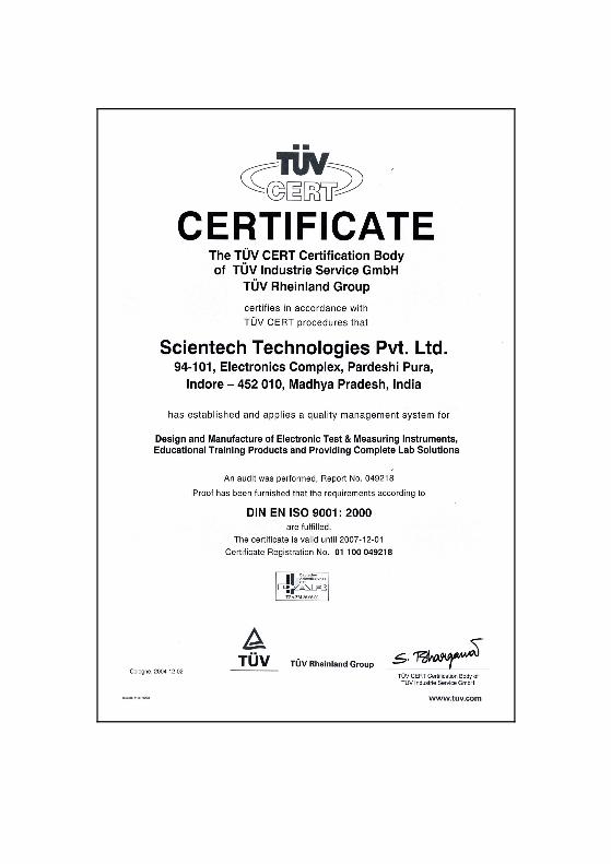
An ISO 9001: 2000 company
94-101, Electronic Complex, Pardesipura INDORE-452010, India.

AB14
Tel.: 91-731-2570301 Fax: 91-731-2555643Email: [email protected] Web: www.scientech.bz
Scientech Technologies Pvt. Ltd. 2
AB14
Scientech Technologies Pvt. Ltd. 3

AB14
DARLINGTON PAIR
AB14
TABLE OF CONTENTS
1. Introduction 4
2. Theory 6
3. Experiments
• Experiment 1 9To calculate the current gain of Darlington pair and β of transistor
• Experiment 2 11To calculate the voltage gain of Darlington pair usingVoltage divider biasing
Datasheet 13
4. Warranty 15
5. List of service Centers 16
6. List of Accessories with AB14 17
7. Notes 18
Scientech Technologies Pvt. Ltd. 4

AB14
INTRODUCTION
AB14 is a compact, ready to use DARLINGTON PAIR experiment board. This board is useful for students to understand the working and operation of Darlington pair configuration. It can be used as stand alone unit with external DC power supply or can be used with SCIENTECH Analog Lab ST2612 which has built in DC power supply, AC power supply, function generator, modulation generator, continuity tester, toggle switches, and potentiometer.
List of Boards :
Model Name
AB01 Diode characteristics (Si, Zener, LED)AB02 Transistor characteristics (CB NPN)AB03 Transistor characteristics (CB PNP)AB04 Transistor characteristics (CE NPN)AB05 Transistor characteristics (CE PNP)AB06 Transistor characteristics (CC NPN)AB07 Transistor characteristics (CC PNP)AB08 FET characteristicsAB09 Rectifier CircuitsAB10 Wheatstone Bridge AB11 Maxwell’s BridgeAB12 De Sauty’s BridgeAB13 Schering BridgeAB15 Common Emitter AmplifierAB16 Common Collector AmplifierAB17 Common Base AmplifierAB18 Cascode AmplifierAB19 RC-Coupled AmplifierAB20 Direct Coupled AmplifierAB21 Class A AmplifierAB22 Class B Amplifier (push pull emitter follower)AB23 Class C Tuned AmplifierAB25 Phase Locked Loop (FM Demodulator & Frequency
Divider / Multiplier)AB28 Multivibrator ( Mono stable / Astable)AB29 F-V and V-F ConverterAB30 V-I and I-V ConverterAB31 Zener Voltage Regulator
Scientech Technologies Pvt. Ltd. 5

AB14
AB32 Transistor Series Voltage RegulatorAB33 Transistor Shunt Voltage RegulatorAB35 DC AmmeterAB39 Instrumentation AmplifierAB41 Differential Amplifier (Transistorized)AB42 Operational Amplifier (Inverting / Non-inverting /
Differentiator)AB43 Operational Amplifier (Adder/Scalar)AB44 Operational Amplifier (Integrator/ Differentiator)AB45 Schmitt Trigger and ComparatorAB49 K Derived FilterAB51 Active filters (Low Pass and High Pass)AB52 Active Band Pass Filter AB53 Notch Filter AB54 Tschebyscheff Filter AB56 Fiber Optic Analog LinkAB57 Owen’s BridgeAB58 Anderson’s BridgeAB59 Maxwell’s Inductance BridgeAB65 Phase Shift OscillatorAB66 Wien Bridge OscillatorsAB67 Colpitt OscillatorAB68 Hartley OscillatorAB80 RLC Series and RLC Parallel Resonance AB81 Kirchoff’s Laws (Kirchoff’s Current Law & Kirchoff’s
Voltage Law)AB82 Thevenin’s and Maximum power Transfer TheoremAB83 Reciprocity and Superposition TheoremAB84 Tellegen’s TheoremAB85 Norton’s theoremAB88 Diode ClipperAB89 Diode ClampersAB90 Two port network parameterAB91 Optical Transducer (Photovoltaic cell)AB92 Optical Transducer (Photoconductive cell/LDR)AB93 Optical Transducer (Phototransistor)AB96 Temperature Transducer (RTD & IC335)AB97 Temperature Transducer (Thermocouple)AB101 DSB Modulator and DemodulatorAB102 SSB Modulator and DemodulatorAB106 FM Modulator and Demodulator
Scientech Technologies Pvt. Ltd. 6

AB14
……… and many more
Scientech Technologies Pvt. Ltd. 7
AB14
THEORY
In recent years, electronics have been integrated into motor speed drives and a variety of switching-type power supplies. This meant that standard discrete components needed to be altered to provide better characteristics. The need for the Darlington pair grew from the limitations of SCRs and triac-type thyristors. Thyristors control current by delaying the turn-on time. The later the pulse is applied to turn them on, the smaller the amount of current they will conduct during each cycle. On the other hand, a transistor uses variable current (0 to saturation), which provides an output current that will be a duplication of the input. This means the transistors will produce an analog signal when an analog signal is provided to its base. The simple bipolar transistor has several limitations including slow switching speeds, low gains, and larger power losses due to the switching process. A family of high-gain transistors called metal-oxide semiconductor field effect transistors (MOSFETs) was produced to address the gain problem, but they did not have the capability of controlling larger currents, so the Darlington pair was designed. The Darlington pair can actually be two discrete transistors that are connected in the driver/output configuration, or they can be a single device that has the two transistors internally connected at the point where it was manufactured as a single package.
For large currents it is standard and good procedure to use a Darlington pair of transistors, rather than a single one, which effectively acts like a single transistor with ß that is the product of the two ßs of the individual transistors.
Darlington transistors are circuits that combine two bipolar transistors in a single device. They provide high current gain (β) and require less space than configurations that use two discrete transistors. In Darlington pairs, transistor collectors are tied together and the emitter of the first transistor is directly coupled to the base of the second transistor. The total gain, which is often 1000 or more, is the product of the gain of the individual transistors. Advantages and Disadvantages :
The key advantage of the Darlington configuration is that the total current gain of the circuit equals the product of the current gain of two devices since its current gain is much higher, Darlington connection can have a very high input impedance and can produce very large outputs current .Darlington connections are used with voltage regulators and power amplifiers. The disadvantage is the larger saturation voltage compared to single transistor configurations. Darlington transistor pairs have more phase
Scientech Technologies Pvt. Ltd. 8

AB14
shift at high frequencies and can become unstable with negative feedback more easily. Darlington transistors also have a higher base-emitter voltage, which is the sum of both base emitter voltages. Figure 1 shown below is a Darlington pair since the emitter current of Q1 is the base current for Q2, the darlington pair has an overall current gain of :
β=β1β2 ……………. (1)Semiconductor manufacturers can put a darlington pair inside a single case like fig 2 known as Darlington transistor ,acts like a single transistor with a very high current gain.
NPN Darlington Pair
Fig. 1
Darlington TransistorFig. 2
Complementary Darlington
Scientech Technologies Pvt. Ltd. 9

AB14
Fig. 3Complementary Darlington is a connection of npn and pnp transistors .the collector current of q1 is the base current of q2. if the pnp transistor has a current gain of β1 and the npn output transistor has a current gain of β2 the complementary Darlington acts like a single pnp transistor with a current gain of β1 β2.The Complementary Darlington is sometimes used is class B push-pull power amplifiers.
Input Current and Input Impedance measurement :
Fig. 4Vin’ is the signal applied with Rs.
Vin is the signal at the input terminal of the Darlington pair with Rs.
Ii is the input current of the Darlington pair which can be measured using the formula
(Vin’-Vin)/Rs ………………(2)
Input Impedance can be measured by
Zin =Vin/Ii ……………..(3)
Note: The range of β for TIP31C lies between 90 to 110.
Scientech Technologies Pvt. Ltd. 10

AB14
EXPERIMENT 1Objective : To calculate the current gain of Darlington pair and β of transistor.
Apparatus required : 1. Analog board AB14.2. DC power supply +12V from external source or ST-2612 Analog
Lab.3. Function Generator ST-4064.4. Oscilloscope.5. Multimeter.6. 2mm patch chords.
Circuit diagram :Circuit used to study the operation of Darlington Pair is shown below :
Fig. 5
Scientech Technologies Pvt. Ltd. 11

AB14
Procedure :• Connect +12V variable dc power supplies at their indicated position
from external source or ST-2612 Analog Lab.
1. Connect +5V dc at Vin’ terminal and connect a patch cord between socket a and socket b.
2. Connect a patch cord between socket e and f.
3. Now measure the dc voltage between base of transistor T1 and using multimeter.
4. Calculate the input current (Ii) by substituting the value in eq.2
5. Now connect +5V directly at the base terminal of transistor T1.
6. Remove the patch cord between socket e and f and connect a multimeter between these sockets to measure the output current (Iout).
7. Calculate the input impedance by using eq.3
8. Calculate the ratio of output current to input current.
9. Ratio of output current to input current gives the overall β of Darlington pair.
10. Individual β of transistors can be calculated by considering the transistors having identical β and substituting in eq.1
Result :
Current Gain of Darlington Pair [Iout / Ii] = ………
Individual β of transistor =.........
Scientech Technologies Pvt. Ltd. 12

AB14
EXPERIMENT 2
Objective : To calculate the voltage gain of Darlington pair using voltage divider
biasing.
Apparatus required :
1. Analog board AB14.
2. DC power supply +12V from
3. Function Generator ST-4064.
4. Oscilloscope.
5. 2mm patch chords.
Circuit diagram :
Circuit used to study the voltage gain of Darlington Pair is shown below :
Fig. 6
Scientech Technologies Pvt. Ltd. 13

AB14
Procedure :
• Connect +12V variable dc power supplies at their indicated position from external source or ST-2612 Analog Lab.
1. Connect a patch cord between socket b and d and also between socket e and f.
2. Connect 1Vp-p, 1 KHz sine wave signal at the input (between points Vin and) of amplifier of AB14 board and observe the same on oscilloscope CH I.
3. Observe the output waveform between points Vout and on oscilloscope CH II.
4. Measure the amplitude of the output waveform on oscilloscope.
5. Calculate the voltage gain Av =Vout/Vin.
Result :
Voltage gain of Darlington pair = ………………………...
Scientech Technologies Pvt. Ltd. 14

AB14
DATASHEET
Scientech Technologies Pvt. Ltd. 15

AB14
Scientech Technologies Pvt. Ltd. 16

AB14
WARRANTY
1. We guarantee the instrument against all manufacturing defects during 24 months from the date of sale by us or through our dealers.
2. The guarantee covers manufacturing defects in respect of indigenous components and material limited to the warranty extended to us by the original manufacturer and defect will be rectified as far as lies within our control.
3. The guarantee will become INVALID.a. If the instrument is not operated as per instruction given in the
instruction manual. b. If the agreed payment terms and other conditions of sale are not
followed.c. If the customer resells the instrument to another party.d. Provided no attempt have been made to service and modify the
instrument.
4. The non-working of the instrument is to be communicated to us immediately giving full details of the complaints and defects noticed specifically mentioning the type and sr. no. of the instrument, date of purchase etc.
5. The repair work will be carried out, provided the instrument is dispatched securely packed and insured with the railways. To and fro charges will be to the account of the customer.
DISPATCH PROCEDURE FOR SERVICE
Should it become necessary to send back the instrument to factory please observe the following procedure :
1. Before dispatching the instrument please write to us giving full details of the fault noticed.
2. After receipt of your letter our repairs dept. will advise you whether it is necessary to send the instrument back to us for repairs or the adjustment is possible in your premises.
Dispatch the instrument (only on the receipt of our advice) securely packed in original packing duly insured and freight paid along with accessories and a copy of the details noticed to us at our factory address.
Scientech Technologies Pvt. Ltd. 17
AB14
LIST OF SERVICE CENTERS
1. Scientech Technologies Pvt. Ltd.90, Electronic Complex Ph : (0731) 5202959Pardesipura, Email : [email protected] INDORE – 452010
2. Scientech Technologies Pvt. Ltd.First Floor, C-19, Ph : (011) 22157370, 22157371F.I.E., Patparganj Industrial Area, Fax : (011) 22157369DELHI – 110092 Email : [email protected]
3. Scientech Technologies Pvt. Ltd.New no.2, Old no.10, 4th street Ph : (044) 42187548, 42187549
Venkateswara nagar, Adyar Fax : (044) 42187549CHENNAI – 600025 Email : [email protected]
4. Scientech Technologies Pvt. Ltd. 202/19, 4th main street Ph : (080) 51285011 Ganganagar, Fax : (080) 51285022 BANGALORE- 560032 Email : [email protected]. Scientech Technologies Pvt. Ltd.
8,1st floor, 123-Hariram Mansion, Ph : (022) 56299457 Dada Saheb Phalke road, Fax : (022) 24168767 Dadar (East), Email : [email protected] MUMBAI –400014 6. Scientech Technologies Pvt. Ltd. 988, Sadashiv Peth, Ph: (020) 24461673 Gyan Prabodhini Lane, Fax: (020) 24482403 PUNE – 411030 Email: [email protected]. Scientech Technologies Pvt. Ltd SPS Apartment, 1st Floor Ph : +913355266800 2, Ahmed Mamoji Street, Email : [email protected]
Behind Jaiswal Hospital, Liluah, HOWRAH-711204 W.B.8. Scientech Technologies Pvt. Ltd Flat No. 205, 2nd Floor, Ph : (040) 55465643 Lakshminarayana Apartments Email : [email protected] ‘C’ wing, Street No. 17, Himaytnagar,
Scientech Technologies Pvt. Ltd. 18

AB14
HYDERABAD- 500029
Scientech Technologies Pvt. Ltd. 19
AB14
LIST OF ACCESSORIES
1. 2mm patch cord (red)................................................................ 1 Nos.
2. 2mm patch cord (blue).............................................................. 2 Nos.
3. 2mm patch cord (black)............................................................ 3 Nos.
Scientech Technologies Pvt. Ltd. 20

AB14
NOTES
Scientech Technologies Pvt. Ltd. 21

AB14
NOTES
Scientech Technologies Pvt. Ltd. 22

AB14
NOTES
Scientech Technologies Pvt. Ltd. 23