a1180, a1181, a1182, and a1183: sensitive two-wire field
TRANSCRIPT

NOTE: For detailed information on purchasing options, contact your local Allegro field applications engineer or sales representative.
Allegro MicroSystems, Inc. reserves the right to make, from time to time, revisions to the anticipated product life cycle plan for a product to accommodate changes in production capabilities, alternative product availabilities, or market demand. The information included herein is believed to be accurate and reliable. However, Allegro MicroSystems, Inc. assumes no respon-sibility for its use; nor for any infringements of patents or other rights of third parties which may result from its use.
Sensitive Two-Wire Field-Programmable Chopper-Stabilized Unipolar Hall-Effect Switches
A1180, A1181, A1182, and A1183
• for the A1180LUA-T use the A1190LUA-T • for the A1180ELHLT-T use the A1190LLHLX-T • for the A1182EUA-T and the A1182LUA-T use the A1192LUA-T • for the A1182ELHLT-T and the A1182LLHLT-T use the A1192LLHLX-T • for the A1183EUA-T and the A1183LUA-T use the A1193LUA-T • for the A1183ELHLT-T and the A1183LLHLT-T use the A1193LLHLX-T
Recommended Substitutions:
Date of status change: October 31, 2011
This device is no longer in production. The device should not be purchased for new design applications. Samples are no longer available.
Discontinued Product
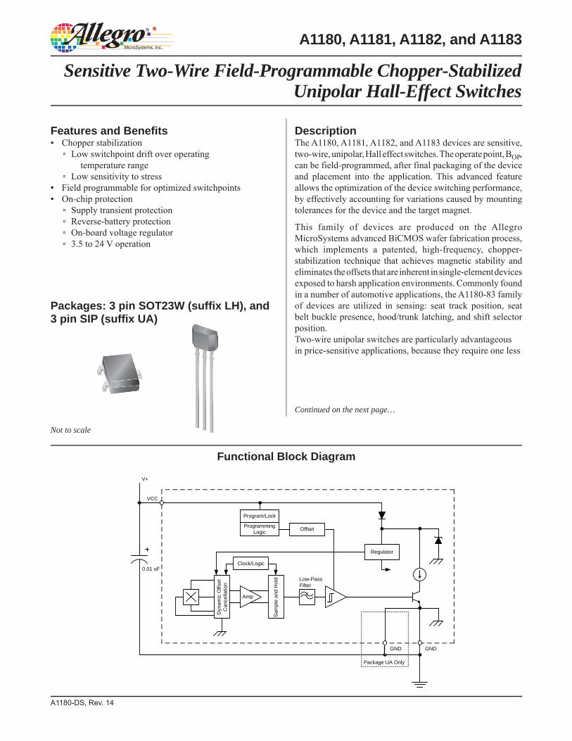
DescriptionThe A1180, A1181, A1182, and A1183 devices are sensitive, two-wire, unipolar, Hall effect switches. The operate point, BOP, can be field-programmed, after final packaging of the device and placement into the application. This advanced feature allows the optimization of the device switching performance, by effectively accounting for variations caused by mounting tolerances for the device and the target magnet.
This family of devices are produced on the Allegro MicroSystems advanced BiCMOS wafer fabrication process, which implements a patented, high-frequency, chopper-stabilization technique that achieves magnetic stability and eliminates the offsets that are inherent in single-element devices exposed to harsh application environments. Commonly found in a number of automotive applications, the A1180-83 family of devices are utilized in sensing: seat track position, seat belt buckle presence, hood/trunk latching, and shift selector position. Two-wire unipolar switches are particularly advantageous in price-sensitive applications, because they require one less
A1180-DS, Rev. 14
Features and Benefits▪ Chopper stabilization
▫ Low switchpoint drift over operating temperature range
▫ Low sensitivity to stress▪ Field programmable for optimized switchpoints▪ On-chip protection
▫ Supply transient protection▫ Reverse-battery protection▫ On-board voltage regulator▫ 3.5 to 24 V operation
Sensitive Two-Wire Field-Programmable Chopper-Stabilized Unipolar Hall-Effect Switches
Continued on the next page…
Functional Block Diagram
Not to scale
Packages: 3 pin SOT23W (suffix LH), and 3 pin SIP (suffix UA)
A1180, A1181, A1182, and A1183
Amp
Regulator
Low-PassFilter
GND
VCC
GND
Package UA Only
0.01 uF
V+
Program/Lock
ProgrammingLogic Offset
Clock/Logic
Dyn
amic
Offs
etC
ance
llatio
n
Sam
ple
and
Hol
d
Sensitive Two-Wire Field-Programmable Chopper-Stabilized Unipolar Hall Effect Switches
A1180, A1181, A1182, and A1183
2Allegro MicroSystems, Inc.115 Northeast CutoffWorcester, Massachusetts 01615-0036 U.S.A.1.508.853.5000; www.allegromicro.com
Selection GuidePart Number Packing1 Mounting Ambient, TA
(°C)Output
South (+) Field2Supply Current at Low
Output, ICC(L) (mA)A1180ELHLT-T3 7-in. reel, 3000 pieces/reel Surface mount
–40 to 85 Low 2 to 5A1180LUA-T4 Bulk, 500 pieces/bag SIP through hole
A1182ELHLT-T4 7-in. reel, 3000 pieces/reel Surface mount–40 to 85
Low
5 to 6.9
A1182EUA-T4 Bulk, 500 pieces/bag SIP through hole
A1182LLHLT-T4 7-in. reel, 3000 pieces/reel Surface mount–40 to 150
A1182LUA-T4 Bulk, 500 pieces/bag SIP through hole
A1183ELHLT-T4 7-in. reel, 3000 pieces/reel Surface mount–40 to 85
HighA1183EUA-T4 Bulk, 500 pieces/bag SIP through hole
A1183LLHLT-T4 7-in. reel, 3000 pieces/reel Surface mount–40 to 150
A1183LUA-T4 Bulk, 500 pieces/bag SIP through hole1Contact Allegro for additional packing options. 2South (+) magnetic fields must be of sufficient strength.3This variant is in production, however, it has been deemed Pre-End of Life. The product is approaching end of life. Within a minimum of 6 months, the device will enter its final, Last Time Buy, order phase. Status change: January 31, 2011. Suggested replacement: A1190LLHLX-T.4Variant is in production but has been determined to be NOT FOR NEW DESIGN. This classification indicates that sale of the variant is currently restricted to existing customer applications. The variant should not be purchased for new design applications because obsolescence in the near future is probable. Samples are no longer available. Status change: January 31, 2011.
wire than the more traditional open-collector output switches. Additionally, the system designer gains inherent diagnostics because output current normally fl ows in either of two narrowly-specifi ed ranges. Any output current level outside of these two ranges is a fault condition. The A1180-83 family of devices also features on-chip transient protection, and a Zener clamp to protect against overvoltage conditions on the supply line.
The output currents of the A1181 and A1183 switch HIGH in the presence of a south polarity magnetic fi eld of suffi cient strength; and switch LOW otherwise, including when there is no signifi cant magnetic fi eld present. The A1180 and A1182 have inverted out-
put current levels: switching LOW in the presence of a south polar-ity magnetic fi eld of suffi cient strength, and HIGH otherwise. The devices also differ in their specifi ed LOW current supply levels.Both devices are offered in two package styles: LH, a SOT-23W miniature low-profi le package for surface-mount applications, and UA, a three-lead ultramini Single Inline Package (SIP) for through-hole mounting. Each package is available in a lead (Pb) free version (suffi x, –T) with 100% matte tin plated leadframe.
Factory-programmed versions are also available. Refer to: A1140, A1141, A1142, A1143, A1145, and A1146.
Absolute Maximum RatingsCharacteristic Symbol Notes Rating Units
Supply Voltage VCC 28 V
Reverse Supply Voltage VRCC –18 V
Magnetic Flux Density B Unlimited G
Operating Ambient Temperature TARange E –40 to 85 ºC
Range L –40 to 150 ºC
Maximum Junction Temperature TJ(max) 165 ºC
Storage Temperature Tstg –65 to 170 ºC
Description (continued)
Sensitive Two-Wire Field-Programmable Chopper-Stabilized Unipolar Hall Effect Switches
A1180, A1181, A1182, and A1183
3Allegro MicroSystems, Inc.115 Northeast CutoffWorcester, Massachusetts 01615-0036 U.S.A.1.508.853.5000; www.allegromicro.com
MAGNETIC CHARACTERISTICS1 over the operating voltage and temperature range, unless otherwise specifi ed
Characteristic Symbol Test Conditions Min. Typ. Max. Units
Programmable Operate Point Range BOPrangeICC = ICC(H) for A1180 and A1182ICC = ICC(L) for A1181 and A1183 60 – 200 G
Initial Operate Point Range BOPinit VCC = 12 V – 33 60 G
Switchpoint Step Size2 BRES VCC = 5 V, TA = 25°C 4 8 12 G
Number of Programming Bits –Switchpoint setting – 5 – Bit
Programming locking – 1 – Bit
Temperature Drift of BOP ∆BOP – – ±20 G
Hysteresis BHYS BHYS = BOP – BRP 5 15 30 G1Relative values of B use the algebraic convention, where positive values indicate south magnetic polarity, and negative values indicate north magnetic polarity; therefore greater B values indicate a stronger south polarity fi eld (or a weaker north polarity fi eld, if present).2The range of values specifi ed for BRES is a maximum, derived from the cumulative programming bit errors.
ELECTRICAL CHARACTERISTICS over the operating voltage and temperature range, unless otherwise specifi ed
Characteristic Symbol Test Conditions Min. Typ. Max. Units
Supply Voltage1 VCC Device powered on 3.5 – 24 V
Supply Current2ICC(L)
B >BOP for A1180; B <BRP for A1181 2 – 5 mA
B >BOP for A1182; B <BRP for A1183 5 – 6.9 mA
ICC(H)B >BOP for A1181, A1183B <BRP for A1180, A1182 12 – 17 mA
Supply Zener Clamp Voltage VZ(supply) ICC = ICC(L)(max) + 3 mA; TA = 25°C 28 – 40 V
Supply Zener Clamp Current IZ(supply) VZ(supply) = 28 V – –ICC(L)(max) + 3 mA
mA
Reverse Supply Current IRCC VRCC = –18 V – – –1.6 mA
Output Slew Rate3 di/dtNo bypass capacitor; capacitance of the oscilloscope performing the measurement = 20 pF
– 36 – mA/μs
Chopping Frequency fC – 200 – kHz
Power-On Time4 tonAfter factory trimming; with and without bypass capacitor (CBYP = 0.01 μF) – – 25 μs
Power-On State5,6 POS ton ≤ ton(max); VCC slew rate ≥ 25 mV/μs – HIGH – –1VCC represents the generated voltage between the VCC pin and the GND pin.2Relative values of B use the algebraic convention, where positive values indicate south magnetic polarity, and negative values indicate north magnetic polarity; therefore greater B values indicate a stronger south polarity fi eld (or a weaker north polarity fi eld, if present). 3Measured without bypass capacitor between VCC and GND. Use of a bypass capacitor results in slower current change. 4Measured with and without bypass capacitor of 0.01 μF. Adding a larger bypass capacitor causes longer Power-On Time.5POS is defi ned as true only with a VCC slew rate of 25 mV / μs or greater. Operation with a VCC slew rate less than 25 mV / μs can permanently harm device performance.6POS is undefi ned for t > ton or BRP < B < BOP .

Sensitive Two-Wire Field-Programmable Chopper-Stabilized Unipolar Hall Effect Switches
A1180, A1181, A1182, and A1183
4Allegro MicroSystems, Inc.115 Northeast CutoffWorcester, Massachusetts 01615-0036 U.S.A.1.508.853.5000; www.allegromicro.com
Characteristic Data
0
2
4
6
8
10
10
12
14
16
18
20
-50 0 50 100 150 2000
2
4
6
8
10
-50 0 50 100 150 200
-50 0 50 100 150 200
-50 0 50 100 150 200 -50 0 50 100 150 200
5
10
15
20
25
30
ICC(L) versus Ambient Temperature at Various Levels of VCC
(A1180, A1181)
Hysteresis versus Ambient Temperature at Various Levels of VCC
(A1180, A1181, A1182, A1183)
ICC(H) versus Ambient Temperature at Various Levels of VCC
(A1180, A1181, A1182, A1183)
Ambient Temperature, TA (°C)
Ambient Temperature, TA (°C)
Ambient Temperature, TA (°C) Ambient Temperature, TA (°C)
I CC
(H) (
mA
)
I CC
(L) (
mA
)A
vera
ge B
OP (G
)
BH
YS (G
)
VCC (V)
3.5
12
24
VCC (V)
3.5
12
24
VCC (V)
3.5
12
24
ICC(L) versus Ambient Temperature at Various Levels of VCC
(A1182, A1183)
Ambient Temperature, TA (°C)
I CC
(L) (
mA
) VCC (V)
3.5
12
24
0
25
50
75
100
125
150
175
200
Average BOP Bits versus Ambient Temperature (A1180, A1181, A1182, A1183)
BOPinit
Bit 1
Bit 2
Bit 3
Bit 4
Bit 5
Sensitive Two-Wire Field-Programmable Chopper-Stabilized Unipolar Hall Effect Switches
A1180, A1181, A1182, and A1183
5Allegro MicroSystems, Inc.115 Northeast CutoffWorcester, Massachusetts 01615-0036 U.S.A.1.508.853.5000; www.allegromicro.com
Device Qualifi cation Program
EMC (Electromagnetic Compatibility) Requirements
Test Name Reference Specifi cationESD – Human Body Model AEC-Q100-002ESD – Machine Model AEC-Q100-003Conducted Transients ISO 7637-2Direct RF Injection ISO 11452-7Bulk Current Injection ISO 11452-4TEM Cell ISO 11452-3
Contact Allegro for information.
Contact your local representative for EMC results.

Sensitive Two-Wire Field-Programmable Chopper-Stabilized Unipolar Hall Effect Switches
A1180, A1181, A1182, and A1183
6Allegro MicroSystems, Inc.115 Northeast CutoffWorcester, Massachusetts 01615-0036 U.S.A.1.508.853.5000; www.allegromicro.com
THERMAL CHARACTERISTICS may require derating at maximum conditions, see application information
Characteristic Symbol Test Conditions* Value Units
Package Thermal Resistance RθJA
Package LH, 1-layer PCB with copper limited to solder pads 228 ºC/W
Package LH, 2-layer PCB with 0.463 in.2 of copper area each side connected by thermal vias 110 ºC/W
Package UA, 1-layer PCB with copper limited to solder pads 165 ºC/W
*Additional thermal information available on Allegro Web site.
6789
2345
10111213141516171819202122232425
20 40 60 80 100 120 140 160 180
Temperature (ºC)
Max
imum
Allo
wab
le V
CC
(V)
Power Derating Curve
(RθJA = 228 ºC/W)1-layer PCB, Package LH
(RθJA = 110 ºC/W)2-layer PCB, Package LH
(RθJA = 165 ºC/W)1-layer PCB, Package UA
VCC(min)
VCC(max)
0100200300400500600700800900
1000110012001300140015001600170018001900
20 40 60 80 100 120 140 160 180Temperature (°C)
Pow
er D
issi
patio
n, P
D (m
W)
Power Dissipation versus Ambient Temperature
(RθJA = 165 ºC/W)
1-layer PCB, Package UA
(RθJA = 228 ºC/W)
1-layer PCB, Package LH
(RθJA = 110 ºC/W)
2-layer PCB, Package LH

Sensitive Two-Wire Field-Programmable Chopper-Stabilized Unipolar Hall Effect Switches
A1180, A1181, A1182, and A1183
7Allegro MicroSystems, Inc.115 Northeast CutoffWorcester, Massachusetts 01615-0036 U.S.A.1.508.853.5000; www.allegromicro.com
Functional Description
BO
PBR
P
BHYS
ICC(H)
I CC
ICC(L)
Sw
itch to Low
Sw
itch
to H
igh
B+B–
I+
0
(A) A1180 and A1182
BO
PBR
P
BHYS
ICC(H)
I CC
ICC(L)
Sw
itch
to H
ighS
witch to Low
B+
I+
B–0
(B) A1181 and A1183
Operation
The output, ICC, of the A1180 and A1182 devices switch low after the magnetic fi eld at the Hall element exceeds the oper-ate point threshold, BOP. When the magnetic fi eld is reduced to below the release point threshold, BRP, the device output goes high. The differences between the magnetic operate and release point is called the hysteresis of the device, BHYS. This built-
in hysteresis allows clean switching of the output even in the presence of external mechanical vibration and electrical noise. The A1181 and A1183 devices switch with opposite polarity for similar BOP and BRP values, in comparison to the A1180 and A1183 (see fi gure 1).
Figure 1. Alternative switching behaviors are available in the A118x device family. On the horizontal axis, the B+ direction indicates increasing south polarity magnetic fi eld strength, and the B– direction indicates decreasing south polarity fi eld strength (including the case of increasing north polarity).

Sensitive Two-Wire Field-Programmable Chopper-Stabilized Unipolar Hall Effect Switches
A1180, A1181, A1182, and A1183
8Allegro MicroSystems, Inc.115 Northeast CutoffWorcester, Massachusetts 01615-0036 U.S.A.1.508.853.5000; www.allegromicro.com
Figure 2. Chopper stabilization circuit (dynamic quadrature offset cancellation)
Amp
Regulator
Clock/Logic
Hall Element
Sam
ple
and
Hol
d
Low-PassFilter
Chopper Stabilization TechniqueA limiting factor for switchpoint accuracy when using Hall effect technology is the small signal voltage developed across the Hall element. This voltage is proportionally small relative to the offset that can be produced at the output of the Hall element device. This makes it diffi cult to process the signal and maintain an accurate, reliable output over the specifi ed temperature and voltage range.
Chopper stabilization is a unique approach used to minimize Hall offset on the chip. The Allegro patented technique, dynamic quadrature offset cancellation, removes key sources of the output drift induced by temperature and package stress. This offset reduction technique is based on a signal modulation-demodula-tion process. The undesired offset signal is separated from the magnetically induced signal in the frequency domain through modulation. The subsequent demodulation acts as a modulation process for the offset causing the magnetically induced signal to recover its original spectrum at base band while the DC offset becomes a high frequency signal. Then, using a low-pass fi lter, the signal passes while the modulated DC offset is suppressed.
The chopper stabilization technique uses a 200 kHz high fre-quency clock. For demodulation process, a sample-and-hold
technique is used, where the sampling is performed at twice the chopper frequency (400KHz). The sampling demodulation process produces higher accuracy and faster signal processing capability. Using this chopper stabilization approach, the chip is desensitized to the effects of temperature and stress. This tech-nique produces devices that have an extremely stable quiescent Hall output voltage, is immune to thermal stress, and has precise recoverability after temperature cycling. This technique is made possible through the use of a BiCMOS process which allows the use of low-offset and low-noise amplifi ers in combination with high-density logic integration and sample-and-hold circuits.
The repeatability of switching with a magnetic fi eld is slightly affected using a chopper technique. The Allegro high frequency chopping approach minimizes the affect of jitter and makes it imperceptible in most applications. Applications that may notice the degradation are those that require the precise sensing of alter-nating magnetic fi elds such as ring magnet speed sensing. For those applications, Allegro recommends the “low jitter” family of digital devices.

Sensitive Two-Wire Field-Programmable Chopper-Stabilized Unipolar Hall Effect Switches
A1180, A1181, A1182, and A1183
9Allegro MicroSystems, Inc.115 Northeast CutoffWorcester, Massachusetts 01615-0036 U.S.A.1.508.853.5000; www.allegromicro.com
Application InformationFor additional general application information, visit the Allegro MicroSystems Web site at www. allegromicro.com.
GND
A118x
VCC
V+
0.01 uF
A
B
BGND
ECU
Package UA OnlyA
B Maximum separation 5 mm
RSENSE
CBYP
Figure 3. Typical application circuit
Typical Application Circuit
The A118x family of devices must be protected by an external bypass capacitor, CBYP, connected between the supply, VCC, and the ground, GND, of the device. CBYP reduces both external noise and the noise generated by the chopper-stabilization func-tion. As shown in fi gure 3, a 0.01 μF capacitor is typical.
Installation of CBYP must ensure that the traces that connect it to the A118x pins are no greater than 5 mm in length.
All high-frequency interferences conducted along the supply lines are passed directly to the load through CBYP, and it serves only to protect the A118x internal circuitry. As a result, the load ECU (electronic control unit) must have suffi cient protection, other than CBYP, installed in parallel with the A118x.
A series resistor on the supply side, RS (not shown), in combi-nation with CBYP, creates a fi lter for EMI pulses. (Additional information on EMC is provided on the Allegro MicroSystems Web site.)
When determining the minimum VCC requirement of the A118x device, the voltage drops across RS and the ECU sense resistor, RSENSE, must be taken into consideration. The typical value for RSENSE is approximately 100 Ω.
Sensitive Two-Wire Field-Programmable Chopper-Stabilized Unipolar Hall Effect Switches
A1180, A1181, A1182, and A1183
10Allegro MicroSystems, Inc.115 Northeast CutoffWorcester, Massachusetts 01615-0036 U.S.A.1.508.853.5000; www.allegromicro.com
Power Derating
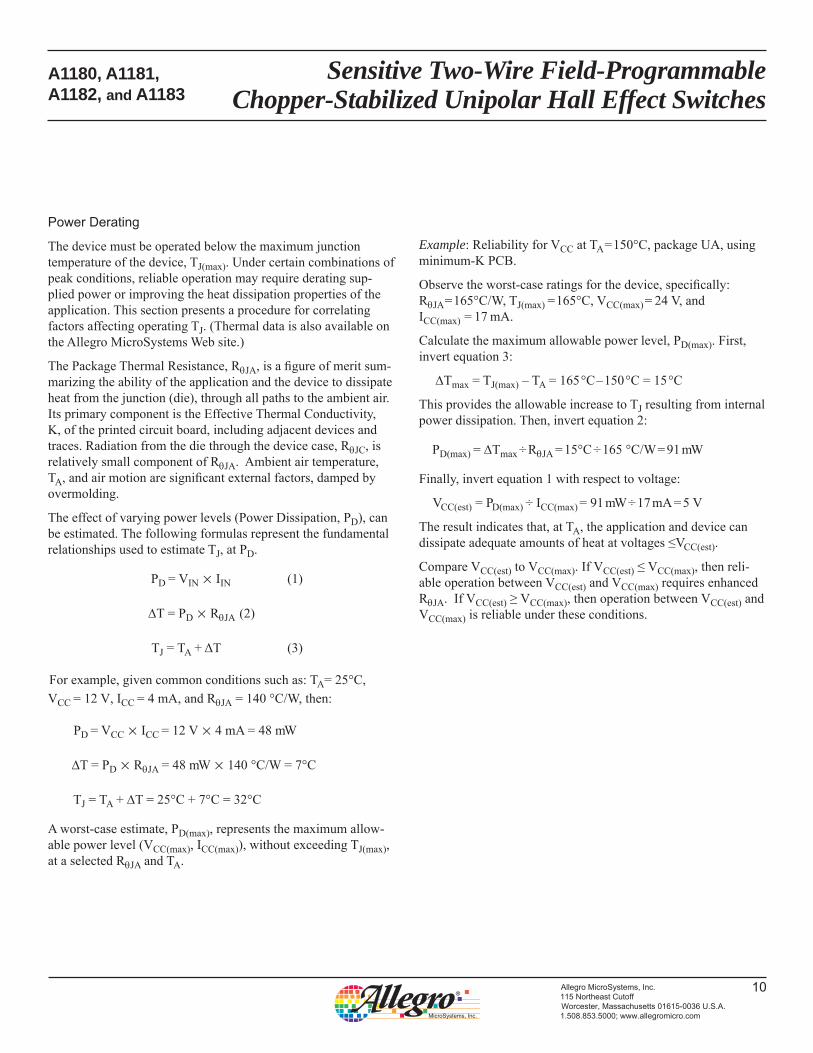
The device must be operated below the maximum junction temperature of the device, TJ(max). Under certain combinations of peak conditions, reliable operation may require derating sup-plied power or improving the heat dissipation properties of the application. This section presents a procedure for correlating factors affecting operating TJ. (Thermal data is also available on the Allegro MicroSystems Web site.)
The Package Thermal Resistance, RJA, is a fi gure of merit sum-marizing the ability of the application and the device to dissipate heat from the junction (die), through all paths to the ambient air. Its primary component is the Effective Thermal Conductivity, K, of the printed circuit board, including adjacent devices and traces. Radiation from the die through the device case, RJC, is relatively small component of RJA. Ambient air temperature, TA, and air motion are signifi cant external factors, damped by overmolding.
The effect of varying power levels (Power Dissipation, PD), can be estimated. The following formulas represent the fundamental relationships used to estimate TJ, at PD.
PD = VIN × IIN (1)
T = PD × RJA (2)
TJ = TA + ΔT (3)
For example, given common conditions such as: TA= 25°C,VCC = 12 V, ICC = 4 mA, and RJA = 140 °C/W, then:
PD = VCC × ICC = 12 V × 4 mA = 48 mW
T = PD × RJA = 48 mW × 140 °C/W = 7°C
TJ = TA + T = 25°C + 7°C = 32°C
A worst-case estimate, PD(max), represents the maximum allow-able power level (VCC(max), ICC(max)), without exceeding TJ(max), at a selected RJA and TA.
Example: Reliability for VCC at TA = 150°C, package UA, using minimum-K PCB.
Observe the worst-case ratings for the device, specifi cally: RJA = 165°C/W, TJ(max) = 165°C, VCC(max) = 24 V, and ICC(max) = 17 mA.
Calculate the maximum allowable power level, PD(max). First, invert equation 3:
Tmax = TJ(max) – TA = 165 °C – 150 °C = 15 °C
This provides the allowable increase to TJ resulting from internal power dissipation. Then, invert equation 2:
PD(max) = Tmax ÷ RJA = 15°C ÷ 165 °C/W = 91 mW
Finally, invert equation 1 with respect to voltage:
VCC(est) = PD(max) ÷ ICC(max) = 91 mW ÷ 17 mA = 5 V
The result indicates that, at TA, the application and device can dissipate adequate amounts of heat at voltages ≤VCC(est).
Compare VCC(est) to VCC(max). If VCC(est) ≤ VCC(max), then reli-able operation between VCC(est) and VCC(max) requires enhanced RJA. If VCC(est) ≥ VCC(max), then operation between VCC(est) and VCC(max) is reliable under these conditions.
Sensitive Two-Wire Field-Programmable Chopper-Stabilized Unipolar Hall Effect Switches
A1180, A1181, A1182, and A1183
11Allegro MicroSystems, Inc.115 Northeast CutoffWorcester, Massachusetts 01615-0036 U.S.A.1.508.853.5000; www.allegromicro.com
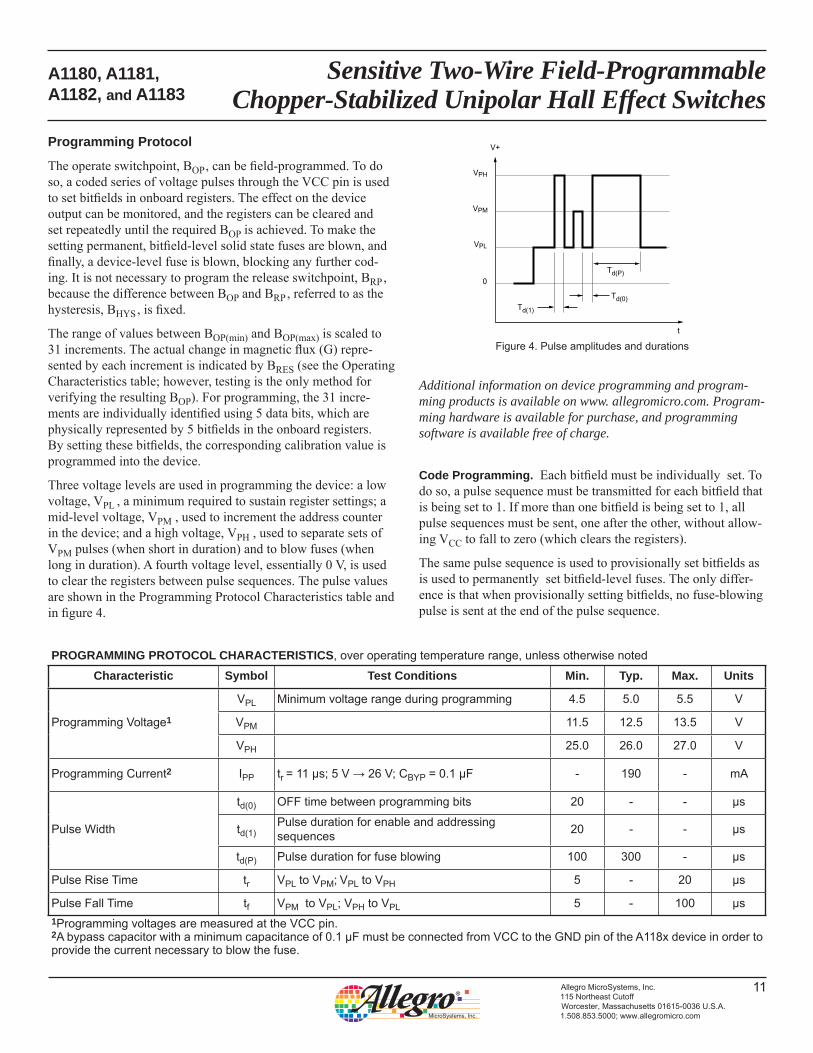
PROGRAMMING PROTOCOL CHARACTERISTICS, over operating temperature range, unless otherwise noted
Characteristic Symbol Test Conditions Min. Typ. Max. Units
Programming Voltage1
VPL Minimum voltage range during programming 4.5 5.0 5.5 V
VPM 11.5 12.5 13.5 V
VPH 25.0 26.0 27.0 V
Programming Current2 IPP tr = 11 μs; 5 V → 26 V; CBYP = 0.1 μF - 190 - mA
Pulse Width
td(0) OFF time between programming bits 20 - - μs
td(1)Pulse duration for enable and addressing sequences 20 - - μs
td(P) Pulse duration for fuse blowing 100 300 - μs
Pulse Rise Time tr VPL to VPM; VPL to VPH 5 - 20 μs
Pulse Fall Time tf VPM to VPL; VPH to VPL 5 - 100 μs1Programming voltages are measured at the VCC pin. 2A bypass capacitor with a minimum capacitance of 0.1 μF must be connected from VCC to the GND pin of the A118x device in order to provide the current necessary to blow the fuse.
VPH
V+
t
VPM
VPL
0
Td(1)
Td(0)
Td(P)
Figure 4. Pulse amplitudes and durations
Additional information on device programming and program-ming products is available on www. allegromicro.com. Program-ming hardware is available for purchase, and programming software is available free of charge.
Programming Protocol
The operate switchpoint, BOP , can be fi eld-programmed. To do so, a coded series of voltage pulses through the VCC pin is used to set bitfi elds in onboard registers. The effect on the device output can be monitored, and the registers can be cleared and set repeatedly until the required BOP is achieved. To make the setting permanent, bitfi eld-level solid state fuses are blown, and fi nally, a device-level fuse is blown, blocking any further cod-ing. It is not necessary to program the release switchpoint, BRP , because the difference between BOP and BRP , referred to as the hysteresis, BHYS , is fi xed.
The range of values between BOP(min) and BOP(max) is scaled to 31 increments. The actual change in magnetic fl ux (G) repre-sented by each increment is indicated by BRES (see the Operating Characteristics table; however, testing is the only method for verifying the resulting BOP). For programming, the 31 incre-ments are individually identifi ed using 5 data bits, which are physically represented by 5 bitfi elds in the onboard registers. By setting these bitfi elds, the corresponding calibration value is programmed into the device.
Three voltage levels are used in programming the device: a low voltage, VPL , a minimum required to sustain register settings; a mid-level voltage, VPM , used to increment the address counter in the device; and a high voltage, VPH , used to separate sets of VPM pulses (when short in duration) and to blow fuses (when long in duration). A fourth voltage level, essentially 0 V, is used to clear the registers between pulse sequences. The pulse values are shown in the Programming Protocol Characteristics table and in fi gure 4.
Code Programming. Each bitfi eld must be individually set. To do so, a pulse sequence must be transmitted for each bitfi eld that is being set to 1. If more than one bitfi eld is being set to 1, all pulse sequences must be sent, one after the other, without allow-ing VCC to fall to zero (which clears the registers).
The same pulse sequence is used to provisionally set bitfi elds as is used to permanently set bitfi eld-level fuses. The only differ-ence is that when provisionally setting bitfi elds, no fuse-blowing pulse is sent at the end of the pulse sequence.

Sensitive Two-Wire Field-Programmable Chopper-Stabilized Unipolar Hall Effect Switches
A1180, A1181, A1182, and A1183
12Allegro MicroSystems, Inc.115 Northeast CutoffWorcester, Massachusetts 01615-0036 U.S.A.1.508.853.5000; www.allegromicro.com
The pulse sequences consist of the following groups of pulses:
1. An enable sequence.2. A bitfi eld address sequence.3. When permanently setting the bitfi eld, a long VPH fuse-blow-
ing pulse. (Note: Blown bit fuses cannot be reset.)4. When permanently setting the bitfi eld, the level of VCC must
be allowed to drop to zero between each pulse sequence, in order to clear all registers. However, when provisionally set-ting bitfi elds, VCC must be maintained at VPL between pulse sequences, in order to maintain the prior bitfi eld settings while preparing to set additional bitfi elds.
Bitfi elds that are not set are evaluated as zeros. The bitfi eld-level fuses for 0 value bitfi elds are never blown. This prevents inad-
vertently setting the bitfi eld to 1. Instead, blowing the device-level fuse protects the 0 bitfi elds from being accidentally set in the future.
When provisionally trying the calibration value, one pulse sequence is used, using decimal values. The sequence for setting the value 510 is shown in fi gure 5.
When permanently setting values, the bitfi elds must be set indi-vidually, and 510 must be programmed as binary 101. Bit 3 is set to 1 (0001002, which is 410), then bit 1 is set to 1 (0000012, which is 110). Bit 2 is ignored, and so remains 0.Two pulse sequences for permanently setting the calibration value 5 are shown in fi gure 6. The fi nal VPH pulse is maintained for a longer period, enough to blow the corresponding bitfi eld-level fuse.
VPH
V+
t
VPM
VPL
0
Encode 001002 (410)
Enable Address
Address
Blow BlowEnable
Encode 000012 (110)
Figure 6. Pulse sequence to permanently encode calibration value 5 (101 binary, or bitfi eld address 3 and bitfi eld address 1).
VPH
V+
t
VPM
VPL
0
Try 510
Enable Address ClearOptional Monitoring
Figure 5. Pulse sequence to provisionally try calibration value 5.
Sensitive Two-Wire Field-Programmable Chopper-Stabilized Unipolar Hall Effect Switches
A1180, A1181, A1182, and A1183
13Allegro MicroSystems, Inc.115 Northeast CutoffWorcester, Massachusetts 01615-0036 U.S.A.1.508.853.5000; www.allegromicro.com
VPH
V+
t
VPM
VPL
0
Address 1Address 2
Address n ( ≤ 31)
Figure 8. Pulse sequence to select addresses
Falling edge of final BOP address digit VPH
V+
t
VPM
VPL
0
Encode Lock Bit
Enable Address Blow
32 pulses
Figure 9. Pulse sequence to encode lock bit
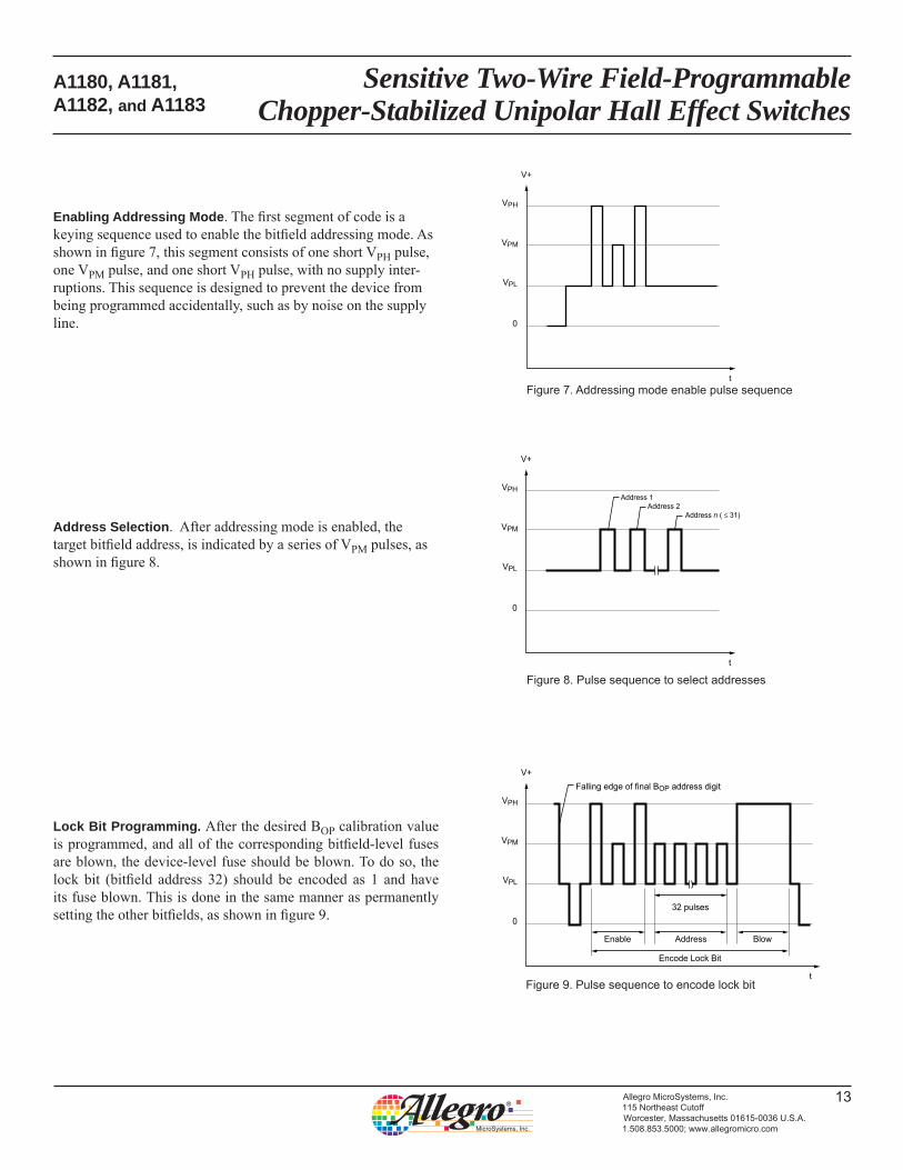
Lock Bit Programming. After the desired BOP calibration value is programmed, and all of the corresponding bitfi eld-level fuses are blown, the device-level fuse should be blown. To do so, the lock bit (bitfi eld address 32) should be encoded as 1 and have its fuse blown. This is done in the same manner as permanently setting the other bitfi elds, as shown in fi gure 9.
Address Selection. After addressing mode is enabled, the target bitfi eld address, is indicated by a series of VPM pulses, as shown in fi gure 8.
Figure 7. Addressing mode enable pulse sequence
VPH
V+
t
VPM
VPL
0
Enabling Addressing Mode. The fi rst segment of code is a keying sequence used to enable the bitfi eld addressing mode. As shown in fi gure 7, this segment consists of one short VPH pulse, one VPM pulse, and one short VPH pulse, with no supply inter-ruptions. This sequence is designed to prevent the device from being programmed accidentally, such as by noise on the supply line.
Sensitive Two-Wire Field-Programmable Chopper-Stabilized Unipolar Hall Effect Switches
A1180, A1181, A1182, and A1183
14Allegro MicroSystems, Inc.115 Northeast CutoffWorcester, Massachusetts 01615-0036 U.S.A.1.508.853.5000; www.allegromicro.com
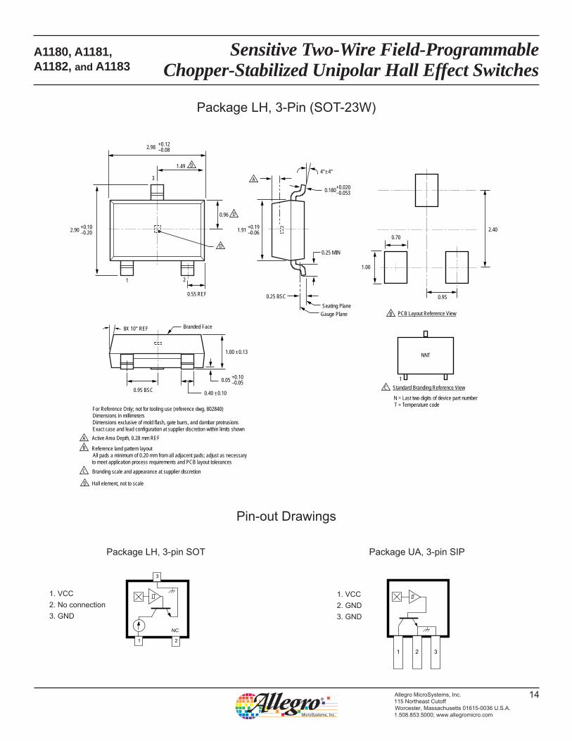
Package LH, 3-Pin (SOT-23W)
Package LH, 3-pin SOT
1. VCC2. No connection3. GND
NC
1 2
3
1 2 3
1. VCC2. GND3. GND
Package UA, 3-pin SIP
Pin-out Drawings
0.55 REF
Gauge PlaneSeating Plane
0.25 BSC
0.95 BSC
0.95
1.00
0.70 2.40
21
A Active Area Depth, 0.28 mm REFB
C
C
B
Reference land pattern layout All pads a minimum of 0.20 mm from all adjacent pads; adjust as necessary to meet application process requirements and PCB layout tolerancesBranding scale and appearance at supplier discretion
A
PCB Layout Reference View
Standard Branding Reference View1
Branded Face
N = Last two digits of device part number T = Temperature code
NNT
2.90 +0.10–0.20
4°±4°
8X 10° REF
0.180+0.020–0.053
0.05 +0.10–0.05
0.25 MIN
1.91 +0.19–0.06
2.98 +0.12–0.08
1.00 ±0.13
0.40 ±0.10
For Reference Only; not for tooling use (reference dwg. 802840)Dimensions in millimetersDimensions exclusive of mold flash, gate burrs, and dambar protrusions Exact case and lead configuration at supplier discretion within limits shown
D Hall element, not to scale
D
D
D1.49
0.96
3

Sensitive Two-Wire Field-Programmable Chopper-Stabilized Unipolar Hall Effect Switches
A1180, A1181, A1182, and A1183
15Allegro MicroSystems, Inc.115 Northeast CutoffWorcester, Massachusetts 01615-0036 U.S.A.1.508.853.5000; www.allegromicro.com
Package UA, 3-Pin SIP
Copyright ©2004-2011, Allegro MicroSystems, Inc.Allegro MicroSystems, Inc. reserves the right to make, from time to time, such de par tures from the detail spec i fi ca tions as may be required to per-
mit improvements in the per for mance, reliability, or manufacturability of its products. Before placing an order, the user is cautioned to verify that the information being relied upon is current.
Allegro’s products are not to be used in life support devices or systems, if a failure of an Allegro product can reasonably be expected to cause the failure of that life support device or system, or to affect the safety or effectiveness of that device or system.
The in for ma tion in clud ed herein is believed to be ac cu rate and reliable. How ev er, Allegro MicroSystems, Inc. assumes no re spon si bil i ty for its use; nor for any in fringe ment of patents or other rights of third parties which may result from its use.
For the latest version of this document, visit our website:www.allegromicro.com
2 31
0.79 REF
1.27 NOM
2.16 MAX
0.51REF
45°
C
45°
B
E
E
E2.04
1.44
Gate burr area
A
BC
Dambar removal protrusion (6X)
A
D
E
D
Branding scale and appearance at supplier discretion
Hall element, not to scale
Active Area Depth, 0.50 mm REF
For Reference Only; not for tooling use (reference DWG-9049)Dimensions in millimetersDimensions exclusive of mold flash, gate burrs, and dambar protrusions Exact case and lead configuration at supplier discretion within limits shown
Standard Branding Reference View
= Supplier emblem N = Last two digits of device part number T = Temperature code
NNT
1
Mold EjectorPin Indent
Branded Face
4.09 +0.08–0.05
0.41 +0.03–0.06
3.02 +0.08–0.05
0.43 +0.05–0.07
15.75 ±0.51
1.52 ±0.05