,a, stc.ange° .ages su.e.s,° -...
TRANSCRIPT

=
VOLUME I OF II
Laboratory Maintenance Instructions
LAUNCH
SATURN V
VEHICLE DIGITAL COMPUTERSimplex Models
NASA Part No. 50M35010
IBM Part No. 6109030
(International Business Machines Corporation)
Contract NAS 8-11561
I
,A, STC.ANGE°.AGESSU.E.S,° I ,=, _t __.i__'_ THE SAME PAGES OF PREVIOUS DATEI /_I_'_ _ 1 Ji%_._I_ _ Insert chonged pages into basicJ _. • nL ._ _'--_._l_'l_-PPl_ publication. Destroy superseded pages.
I---_ _'-- t_O,l_
VOLUME I
GENERAL
""_ _ h i n_ _o n_, _ z a "'ozJtj_• C.. ,?,0,
DESCRIPTION AND THEORY
30 NOVEMBER 1964
CHANGED 4 JANUARY 1965

[ L,sTE ,CT,V,P,0,SI INSERT LATESTCHANGED PAGES. DESTROY SUPERSEDEDPAGES.
TOTAL NUMBER OF PAGES IN VOLUME I IS 226 CONSISTING OF THE FOLLOWING:
Page No. Issue Page No. Issue
*Title .......... 4 Jan 65
*A ............ 4 Jan 65
*i ............. 4 Jan 65
ii Blank ........ Original
iii thru iv ....... Original*v ............. 4 Jan 65
vl Blank ........ Original
vii ........... Originalviii Blank ....... Original
ix ............ Original
x Blank ........ Original
1- 1 ........... Original"1-2 ........... 4 Jan 65
I-3 thru 1-4 ..... Original"1-5 thru 1-7 ..... 4 Jan 65
1- 8 ........... Original
2-1 thru 2-14 .... Original"2-15 .......... 4 Jan 65
2-16 thru 2-33 .... Original
2-34 Blank ...... Original*2-35 .......... 4 Jan 65
2-36 thru 2-51 .... Original*2- 52 thru 2- 53 .... 4 Jan 65
2- 54 .......... Original*2-55 .......... 4 Jan 65
2- 56 .......... Original*2- 57 .......... 4 Jan 65
2- 58 thru 2- 70 . . . Original*2-71 .......... 4 Jan 65
2- 72 thru 2-108... Original"2-109 ......... 4 Jan 65
2-110 thru 2-121 . . Original"2-122 ......... 4 Jan 65
2-123 thru 2-143 . . Original"2-144 ......... 4 Jan 65
2-145 thru 2-159 . . Original"2-160 thru 2-162 . .4 Jan 65
'2-163 thru
2-177 Added .... 4 Jan 65
*2-178 Blank
Added ........ 4 Jan 65
Logic Symbols-1 thru 9 ....... Original
* 10 ........... 4 Jan 65
Glossary-
1 thru 13 ...... Original14 Blank ...... Original
Index-
* 1 ........... 4 Jan 65
2 ........... Original* 3 ........... 4 Jan 65
4 Blank ....... Original
*The asterisk indicates pages changed, added, or deleted b)' the current change.
A Changed 4 January 1965

Volume I
TABLE OF CONTENTS
'._2
Section
II
Title Page
LIST OF ENGINEERING CHANGES ................. vii
LIST OF RELATED MANUAIZ .................... ix
INTRODUCTION AND DESCRIPTION ................ 1-1
1-1.
1-8.1-17.
Introduction ........................... 1-1Structural Description .................... 1-2
1-6Electrical Description . . . .................
THEORY OF OPERATION ....................... 2-1
2-1.
2-4.2-6.2-47.2-52.2-57.2-61.2-62.2-88.2-140.2-192.2-209.2-271.2-303.2-418.2-423.2-430.
Scope and Purpose ....................... 2-1Computer Organization .................... 2-1Functional Organization ................... 2-1Word Organization ....................... 2-10Timing Organization ...................... 2-11Instruction Organization ................... 2-13
Computer Logic Circuits ................... 2-13Timing Element ......................... 2-13Memory Element ........................ 2-32Memory Control Element .................. 2-59Data Control Element ..................... 2-85Program Control Element .................. 2-91Arithmetic Element ................... . . . . 2-117Multiply-Divide Element ................... 2-131Delay Lines ........................... 2-174Voting Element ......................... 2-175Computer Operations ..................... 2-176
Logic Symbols .................. Logic Symbols-1Glossary .......................... Glossary-1Index ............................... Index- 1
-._j
Changed 4 January 1965 i/ii

_ x_ r

Volume I
LIST OF ILLUSTRATIONS
-,..j
Figure Title Page
1-11-2
1-31-4
1-5
1-61-7
1-8
2-12-2
2-3
2-42-5
2-62-7
2-82-92-10
2-112-12
2-13
2-142-152-16
2-17
2-182-192-202-21
2-222-23
2-242-25
2-26
2-272-282-29
2-30
2-3!2-322-33
2-342-35
Computer Assemblies ........................... 1-3Logic Printed Circuit Cables ..................... 1-4
Page Assembly ............................... 1-4Reference Designator Arrangement ................. 1-5
Page Assembly Location Guide .................... 1-7Voltage/Function Listing ........................ 1- 8
Voter Circuits, Block Diagram .................... 1-8Channel Module Arrangement, Block Diagram ......... 1-8
Computer Functional Block Diagram ................ 2-3Data Word Layout ............................ 2-10
Instruction Word Layout ........................ 2-11Computer Timing Organization .................... 2-12
Operation Code Map ........................... 2-14Selecting An Instruction ........................ 2-15
Operand Address ............................. 2-15List of Instructions (5 Sheets) .................... 2-16PIO Addresses (2 Sheets) ........................ 2-21
Clock Generator Block Diagram ................... 2-23
Buffer-Amplifier ............................. 2-24Timing Logic ............................... 2-25Clock Drivers ............................... 2-27
Clock Generator Timing ........................ 2-28
Timing Gate Generator Block Diagram .............. 2-28Control Circuit .............................. 2-28
Shift Register ............................... 2-30Phase Generator ............................. 2-31
TBC Latch ............ , . . . . ................. 2-31Computer Tirning ............................. 2-33Memory Element Block Diagram .................. 2-35Ferrite Core Characteristics ..................... 2-36
6 x 6 Core Plane ............................. 2-37
Core Array Windings .......................... 2-39Memory Module Block Diagram .................. . 2-41
Toroidal Core Array .......................... 2-42Drive Line Assignments ........................ 2-43
Memory Clock Drivers ......................... 2-44
Memory Timing Diagram ................. ...... 2-46El Driver Logic Symbol ........................ 2-47Paired El Drivers ............................ 2-47Y Drive Line Selection ......................... 2-49
X Drive Line Selection ......................... 2-50
Timing Pulse Assignments ...................... 2-51
Inhibit Driver And Winding ....................... 2-52
j
111

Volume I
LIST OF ILLUSTRATIONS (cont)
Figure Title Page
2-362-372-38
2-392-402-412-422-432-442-452-462-472-482-492-502-512-522-532-542-552-562-572-582-592-602-612-622-632-642-652-662-672-682-692-702-712-722-732-742-752-762-772-782-79
Memory Sense Amplifier and Winding ............... 2-53Error Detector Logic Symbol .................... 2-54Temperature Controlled Voltage (TCV) Regulator Logic
Symbol ................................... 2- 55Memory Address Decoding ...................... 2-57Memory Addressing Diagram ..................... 2-58Memory Buffer Register, Typical Latches ............ 2-60Memory Buffer Register Timing Circuits ............. 2-61Memory Address Block Diagram .................. 2-62Lo X Decoder ............................... 2-63Lo Y Deocder ............................... 2-64Hi X Decoder ............................... 2-65Hi Y Decoder ............................... 2-66Syllable Select Latches ......................... 2-68Memory Sync Timing Block Diagram ................ 2-69Memory Sync Timing Circuit ..................... 2-71Memory Read Sync Timing Diagram ................ 2-72Memory Store Sync Timing Diagram ................ 2-73Memory Mode and Module Select Block Diagram ........ 2-75Memory Module Registers ...................... 2-76Memory Module Select Gates ..................... 2-78Memory Module Select Control Circuit .............. 2-79Exclusive Or (XOR) Circuits ..................... 2-80A Memory Parity Check Circuit ................... 2-81Memory Error Monitor Circuit ................... 2-82Memory Buffer Select Latches .................... 2-84Transfer Register (2 Sheets) ..................... 2-86Transfer Register Simplified Block and Timing ........ 2-89Parity Counter .............................. 2-91Parity Counter Timing ......................... 2-92Address Register and Transfer Address Latch ......... 2-94Address Register Timing ....................... 2-95Sector Registers and Control Latches ............... 2-96Data and Instruction Sector Register Timing ........... 2-98Operation Code Register ........................ 2-99Operation Code Register Timing ................... 2-100Operation Decoders (2 Sheets) .................... 2-102Interrupt Control ............................. 2-106Start-Stop Control ............................ 2-107HOP Constant Serializer ........................ 2-109
Automatic HOP Save Circuit Timing ................ 2-111Delay Circuits .............................. 2-112STMD Latch ................................ 2-113Instruction Counter (2 Sheets) .................... 2-114Instruction Counter Timing ...................... 2-116
iv

Volume I
.
LIST OF ILLUSTRATIONS (cont)
,.j
Figure Title Page
2-802-812-822-832-842-852-862-872-882-892-902-912-922-932-942-952-96
2-972-982-992-1002-1012-1022-1032-1042-1052-1062-I072-i082-i092-1102-1112-112
Arithmetic Element Block Diagram ................. 2-118Arithmetic Element (2 Sheets) .................... 2-120Arithmetic Element General Timing ................ 2-122ZER Latch UTR-UACCO Latch Timing .............. 2-124
A/S Circuit, Simplified ........................ 2-126A/S Circuit Truth Table ........................ 2-127LSD-Shift Timing ............................. 2-130MSD-Shfft Block Diagram ....................... 2-132MSD-Shfft Timing ............................ 2-133Table of Delta Values .......................... 2-138
Table of Multiplier Bit Effective Values .............. 2-139Multiply Circuits, Block Diagram .................. 2-142Command Circuit ............................. 2-143
Multiply-Divide Timing Latches ................... 2-144Phase Counter .............................. 2-145
Multiplicand Register, Block Diagram ............... 2-146Multiplier and Product-Quotient Registers, Block
Diagram ................................. 2-147Partial Product Register, Block Diagram ............ 2-147Multiplicand-Divisor Register .................... 2-148Multiplier Quotient and Product-Quotient Registers ...... 2-149Partial Product-Remainder Register (4 Sheets) ......... 2-151Multiply Timing Diagram ....................... 2-155Multiply Computation Cycle Flow Diagram ............ 2-159Sample Restoring Divide Problem .................. 2-162Sample Nonrestoring Divide Problem ............... 2-163Nonrestoring Divide with Signal Shortcut ............. 2-165Truth Table for Second Quotient Bit ................ 2-166Divide Circuit, Block Diagram ................... 2-167Divisor Register, Block Diagram .................. 2-170Quotient and Product- Quotient Registers ............ 2-171Remainder Register, Block Diagram ................ 2-172Delay Line, Simplified Diagram ................... 2-174Voter Circuits ............................... 2-177
Changed 4 January 1965 v/vi


.._2
LIST OF ENGINEERING CHANGES
The following list of Engineering Changes applies to the Breadboard IImodel of the computer. Each letter or pair of letters represents a
different Engineering Change.
EC Number
66109 EM, ER, GE, GM, GZ, HD, KR, KZ, LD through
LH, LJ, LM
66123 HK, KB, LD, NP, PK, PL, PM, SF, SW, WM
66124 AthroughH, JthroughN, P, R, S, T, V, W, Z
AA, AB, AD through AH, AJ through AN, AP,AR, AS, AT, AV, AW, BA through BH, BJ through
BN, BP, BR, BS, BT, BV, BW, BZ, CA, CC
through CH, CJ through CN, CP, CR, CS, CT,CV, CW, CZ, DA through DH, DJ through DN,
DR, DS, DV, DW, DZ, EA, EC through EH, EJthrough EN, EP, ER, ES, ET, EV, EW, EZ,
FA through FH, FJ through FM, FP, FR, FS,FT, FV, FW, FZ, GA through GH, GJ through
GK, GM, GN, GP, GR, GS, ST, GV, GW, GZ,HA through HH, HJ, HK, HL, HN, HP, HR, HT,
HV, HW, HZ, JA through HG, JJ through JM,
JP, JR, JS, JT, JV, JW, JZ, KB, KC, KD, KF,KG, KJ, KL, KM, KN, KR, KS, KT, KV, KW,LA
66125 C, F, K, Z, AH, AK, AN, BB, BC, BF, BG,
BM, BS, BT, CA, CG, CR, CT, DA, DV
66126 K, AF, AM, BF, CG, DH
66127 AD, AF, AH, AK
J
vii/viii

_J
,j

LIST OF RELATED MANUALS
Manual Title
Technical Manual, Laboratory Maintenance Instructions, LaunchVehicle Data Adapter (Simplex Models)
Technical Manual, Checkout Procedures, for Saturn Launch VehicleDigital Computer and Data Adapter
Technical Manual, Laboratory Maintenance Instructions, Saturn VTest Equipment, Vol. I, Vol. II, Vol III
L /x


J
SECTION I
INTRODUCTION AND DESCRIPTION
.....2
-...2
1-1. INTRODUCTION.
1-2. PURPOSE OF MANUAL. This manual contains the laboratory maintenance instruc-tions for breadboard model II of the Launch Vehicle Digital Computer (LVDC), NASA
part number 50M35010, IBM part number 6109030, manufactured by International Busi-ness Machines Corporation, Federal Systems Division, Rockville, Maryland, under con-tract number NAS 8-11561.
1-3. The Launch Vehicle Digital Computer, breadboard H Model is hereafter referredto as the computer.
1-4. This manual is divided into two volumes with descriptive material and supportingdiagrams in volume I and procedural material and reference diagrams in volume II. Theindex and all appendices are included with volume I. Volume I may be used separatelyfor training; volume I and volume II should be used together for maintenance. Thisarrangement increases the handling convenience of the manual.
1-5. Within volume I frequently referred to diagrams are printed only on one side sothat they may be detached and referenced while reading the text. Included in the binder'spocket is a plastic-covered timing diagram. This diagram is a duplicate of the referencedtiming diagram and is supplied as a special aid to the reader.
1-6. PURPOSE OF EQUIPMENT. The computer performs four functions in the SaturnV Launch Vehicle: pre-launch checkout, guidance from launch to parking orbit, orbitalcheckout, and back-up guidance from parking orbit to lunar transfer trajectory. Thebreadboard II model is provided for evaluation only, and will not be used in flight.
1-7. BASIC CHARACTERISTICS. The basic characteristics of the computer are as fol-lows:
TYPE- binary, serial, general purpose, stored program.
ACCURACY -- Add/Subtract: 2-25; Multiply/Divide: 2 -23.
SPEED -- 512,000 bits per second serial; Add: 82 usec; Multiply:328 usec; Divide: 656 usec.
MEMORY -- Ferrite core, random access, 4, 095 locations of 28bits each memory; two self-contained memory modules.
• ARITHMETIC -- Fixed point, 2's complement.
PROGRAMMING -- 18 instruction codes consisting of 10 arithmeticinstructions, 6 program control instructions, 1 input/output in-struction, and 1 store instruction.
ELECTRONICS -- Current-switching diode logic (positive), micro-miniature packaging.
1-1

WORD MAKE-UP -- Data word: Sign + 25 magnitude bits; Instructionword: 4 operation code +9 operand address bits.
TIMING -- 4-clock system, clock repetition rate: 2.048 MC; bit time:
1. 953 microseconds; phase time: 14 bit times; computer cycle: 3phase times.
• INPUT/OUTPUT -- Program controlled, serial.
1-3. STRUCTURAL DESCRIPTION.
1-9. GENERAL. The computer (figure 1-1) measures approximately 29-1/2"x12-1/2"x
10-1/2" and weighs approximately 72-1/2 pounds. Electrical inputs and outputs are sup-plied through eight 55-pin connectors numbered J1 through J8. Directly beneath connec-
tor J8 is a time indicator which records the total operating hours of the computer.
1-10. The connectors are located in the front side of the computer. Connectors J5
through J8 and tile time indicator are adjacent to the right side. Proceeding clockwise,the remaining sides are bottom, left and top, respectively. Orientation may be quickly
established by remembering that the time indicator is located in the bottom right cornerof the front side.
1-11. The computer consists of two major sections, the logic section and the memory
section. The two sections are electrically interconnected by four pluggable printed cir-cuit cables.
1-12. LOGIC SECTION. The logic section consists of a frame assembly, five panel as-
semblies, and a number of page assemblies or "pages". The pages slide into mountinggrooves in the frame assembly and are electrically interconnected by the panel assem-
blies. The panel assemblies, which are mounted on the back of the frame assembly,contain sockets into which the pages are plugged. The panel assemblies are intercon-
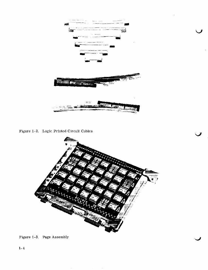
nected by printed circuit cables mounted on terminal blocks. (See figure 1-2.) (The
printed circuit cables and terminal blocks are mounted on the rear of the back panelsand cannot be seen in figure i-i. )
1-13. The panel assemblies are connected to the eight interface connectors by means of
individual wires from the connector pins to the terminal block on the panel assembly.
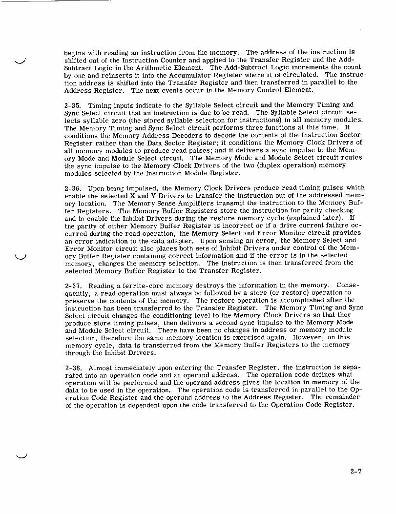
1-14. The page assembly (figure 1-3) has logic components located on both sides, called
A and B. Thirty-six test points, 18 on each side, are available at the top of each page.The test points are found in groups of nine on either side of the "through" pins also found
at lhe top of the page. The "through" pins provide interconnection between the logic cir-cuits on either side of the page.
1-15. MEMORY SECTION. The memory modules are seK-contained assemblies with
memory timing, drive, inhibit, and sensing circuits arranged around the core array.The modules are mounted on the memory plate assembly and electrically connected to
the memory plate assembly by means of a pluggable harness. The printed circuit cablesmentioned earlier then connect the memory to the logic via the memory plate assembly.
1-16. REFERENCE DESIGNATORS. Figure 1-4 illustrates the reference designatorsthat have been assigned to the major assemblies, connectors, and terminal blocks. In
the logic section, the combination of a panel assembly and the attaching pages comprisesa "channel. " Figure 1-5 illustrates where the pages (by part number and logic function)
k.]
r _
k.]
1-2 Changed 4 January 1965

PRINTED CIRCUIT CABLES
MEMORY DISTRIBUTION
BOARD ASSEMBLY
MEMORY ASSEMBLY
'A_ORY SECTION
000O,
ELECTRICALCONNECTORS
PANEL ASSEMBLIES1 THROUGH 5
PAGE ASSEMBLY
!
TIME
INDICATOR
FRAME ASSEMBLY
Figure 1-1. Computer Assemblies
I-3
m
k3
Figure 1-2. Logic Printed Circuit Cables
t
Figure 1-3. Page Assembly
1-4

,,j
EEEE
EEEEE
E
A18
A17
A16
AI5
A14
A13 E6 r
A12 o-
>-
A9 :_ E4
]ABA7 E3
(SPARE)
IA6
"IA5
A4 E2
I A3 El
IA2
"JAI
IJl IJ2 I J3 IJ4
A6 MEMORY PANEL ASSEMBLY (6111323)
J1 J2 J3 J4
E8 A2 A3 A4 A5 A6 A7 A8 A9 AI0
A3 PANEL ASSEMBLY (6108758) E4 ,
E7 AI2 AI3 AI4 AI5 AI6 AI7 AI8 A19 A20r'--_ r'--'1 _ i--'_ l'T'-nr--'n r"-n r"-m r-'-'l
IJ5 J6 J7 J8 |
I-'1 r'-I I"-I I--I i--i r"-i r--i r--! I
I=_.o..II=_.o.Yl P 'I"°_°'_II"°_,u"I ''E3."''ES''E7
A17 r
I IL'--'JL---II II II I J__A3 A. A5A6A7ABA_A,0 ]E61_
E4
All AI2
Z
F CONNECTOR r_ PAGE
• PANEL ASSEMBLY (6108758) E4
[LJ A11 A12 AI3 A14 A15 A16 A17 A18 A19 A20
r _ _ P_I r_l jA_I 5 [_I
A'6r
A15[
AI4[
A13 c
A12[
All[
AI0E
A_["
ABr
A,J-
,,6["
A_J"
A,J"
A3r
A2r
A,J"
FRAME ASSEMBLY
3
"3
J5 J6 J7l J8f_l I'_11'--I r--'l
*PRINTED CIRCUIT CABLES**WIRE BUNDLES
Figure 1-4. Reference Designator Arrangement
Changed 4 January 1965 1-5

have been connected to the panel assemblies. Signals are prefixed with their reference
designators. Thus, if signal ZER were located on the A side of the page in the A10 posi-tion of channel 1, its full title would be A1A10A-ZER.
1-17. ELECTRICAL DESCRIPTION.
1-18. VOLTAGE DISTRIBUTION. All DC power for the computer is supplied by thedata adapter. The voltages and their functions are listed in figure 1-6. Figure 3-2 con-tains the input connector-pin locations for these inputs from the data adapter.
1-19. TRIPLE MODULAR REDUNDANCY (TMR). A failure of virtually any circuit inthe computer, even a momentary failure, could conceivably cause intolerable errors incomputation. To prevent such errors, the computer circuits are redundant in the formof three identical sets, or channels, of logic. Signals from the three channels are fed to
"voter" circuits which sense the majority input. Any differing signal is thereby "out-voted" by two unanimous signals (figure 1-7).
1-20. Each channel is divided into seven aggregates of circuits called modules (figure1-8). Each module has an average of 15 outputs which are voted. Errors from any onemodule are outvoted before they can be passed on to succeeding modules. Thus, it ispossible to have numerous failures without affecting operation, provided that two identicalfailures do not occur simultaneously.
NOTE
The breadboard II model contains only onechannel of logic. Provision is made to hold themissing-channel inputs of the voters to a "tievote", i.e., one "0" and one "1". The existingchannel signal then breaks the tie, and the outputof the voter is always equivalent to the existingchannel input.
1-21. DISAGREEMENT DETECTORS. Since the voter outputs mask errors by providingcorrect outputs, a circuit called a disagreement detector is provided. This circuit pro-vides an output when one of the inputs to a voter differs from the other two.
NOTE
No disagreement detectors are provided Withthe breadboard II model.
1-6 Changed 4 January 1965

_...J
o
!
tD
Changed 4 January 1965 1-7

Voltage Function
V1 Ol thru V1 24
V1 MEM1 thru V1 MEM3
V3 MEM1, V3 MEM2
V3 01 thru V3 10
V4 M1 thru V4 M7
V5 01, V5 02
V5 MEM1, V5 MEM2
+6 volts applied to logic
+6 volts applied to memory
-3 volts applied to memory
-3 volts applied to logic
+6 volts used for module switching
+12 volts applied to logic
+12 volts applied to memory
V5 M1 thru V5 M7
V20 0i, V20 02
V20 AM1, V20 AM2
V2O BM1, V20 BM2
+12 volts used for module switching
+20 volts applied to logic
+20 volts applied to even memory
+20 volts applied to odd memory
Figure 1-6. Voltage/Function Listing
TO DISAGREEMENT DETECTOR
(CHANNEL I) A
(CHANNEL 2) B
(CHANNEL 3) C-
I
l)-
i
q
-4-q_-
m
j VOTER J D
_J VOTER J E
TRUTH TABLE
A B C D,E&F
0 0 0 0
0 0 I 00 I 0 0
0 1 1 11 0 O! 0
1 0 1 11 1 0 1
1 1 1 1
Figure 1-7. Voter Circuits, Block Diagram
i d °°u,C.A""_I I_ l_d I_II_, _CHANNEL
3
Figure 1- 8.
NOTE: VOTER CIRCUIT IS SHOWN AS FOLLOWS --_)--.FOR PURPOSES OF CLARITY, ONLY ONE VOTERINPUT IS SHOWN CONNECTED.
Channel - Module Arrangement, Block Diagram
%J
1-8

x_2
SECTION II
THEORY OF OPERATION
-.M
2-i. SCOPE AND PURPOSE.
2-2. This section describes the operation of the computer. Descriptions containedherein are provided to enable maintenance personnel to understand the operation of thecomputer at the basic logic-block level.
2-3. First, the general organization of the computer is presented to provide a frame-work into which details may be fitted. Next, the logic circuits are divided into "func-tional elements" with each element being described in detail. Finally, the functionalelements are tied together by detailed descriptions of all the computer operations.
2-4. COMPUTER ORGANIZATION.
2-5. The following paragraphs describe the organization of the computer from the as-pects of its functional organization, its word layout and timing, and the instructions itperforms.
2-6. FUNCTIONAL ORGANIZATION
2-7. The LVDC is a general purpose computer which, under control of a stored program,processes data using fixed point, two's complement arithmetic. Data is processed seri-ally in two arithmetic sections which can, if desired, operate concurrently. Addition,subtraction, and logical extractions are performed in one arithmetic section while multi-plication and division are performed in the other.
2-8. The principal storage device is a random access ferrite-core memory with sepa-rate controls for data and instruction addressing. The memory can be operated in eithera simplex or duplex mode. In duplex operation, memory modules are operated in pairswith the same data being stored in each module. Readout errors in one module are cor-rected by using data from its mate to restore the defective location. In simplex opera-tion, each module contains different data which doubles the capacity of the memory.However, simplex operation decreases the reliability of the computer since the abilityto correct readout errors is sacrificed. The memory operating mode is program con-trolled. Temporary storage is provided by static registers composed of latches and byshift registers composed of delay lines and latches.
2-9. The computer is composed of the following eight functional elements:
(1) Timing (5) Program Control
(2) Memory (6) Arithmetic
(3) Memory Control (7) Multiply-Divide
(4) Data Control (8) Voting
2-1

Figure 2-1 is a block diagram of the computer showingthe major parts of eachfunctionalelement (exceptthe Voting Element)andhowthey are interconnected. The heavylineson the diagram showmajor pathsof information flow.
2-10. The Timing Element developsthree levels of standardtiming signals which syn-chronizeand control logic operationsin the remaining sevenelements. Direct outputsof the Timing Element are usedin every functional elementexceptthe Memory Elementwhich generatesits owntiming signals.
2-11. Memory Element. The Memory Element and the Memory Control Element oper-ate together to store the programmed instructions and the constants and data required bythe program. The Memory Element is composed of up to eight memory module assem-blies, each of which contains a ferrite-core array and all the circuits necessary to trans-fer data to and from it. The Memory Control Element determines when a transfer will
occur and selects both the direction of transfer and the memory location to be exercised.Buffer storage for data enroute between the memory and the central computer is also lo-cated in the Memory Control Element.
2-12. In addition to controlling data transfers, the Memory Control Element determinesthe mode (simplex or duplex) in which the memory will operate. In duplex operation,the memory modules are divided into two groups, effectively forming two separate mem-ories with identical contents. The even numbered modules make up the "A" memory andthe odd numbered modules make up the "B" memory. Each module in the A memory ispaired with a module in the B memory which contains the same information. The Mem-
ory Control Element selects both modules of a pair and provides separate buffer storagefor each memory. The two memories are operated simultaneously but the computer usesinformation from only one memory. The Memory Select and Error Monitor circuit de-termines which memory will be used and changes the selection when an error is detectedin the active memory. The Memory Select and Error Monitor circuit continuously sam-ples the drive currents in each memory and checks the parity of each word transferredout of both memories. In simplex operation, each module contains different informationand only one module is selected at a time. The Memory Select and Error Monitor cir-cuit then makes the memory selection follow the selected module so that the B memoryis active when an odd numbered module is selected and the converse. In simplex opera-tion the ability to correct errors is sacrificed.
2-13. Data and constants are stored in the memory in two segments called syllables.Thus, the memory is described as being divided into syllables. One syllable of data istransferred to or from the memory at a time; consequently, two memory cycles arenecessary to transfer a complete data word. Instructions are only half the length of datawords and thus are stored one per syllable. The syllable selection for instructions isstored in the Syllable Select circuit of the Memory Control Element. Timing signalsdetermine whether the stored selection will be used or the selection will be sequenced toread both syllables of a data word.
2-14. When a memory operation is required, the Memory Control Element provides async impulse to the Memory Element. Memory Mode and Module Select circuits direct
the impulse to two memory modules for duplex operation or one module for simplex.Once impulsed, each memory module generates all the timing signals and drive currentsrequired to complete its cycle.
2-15. The Memory Clock Drivers produce either read or store timing pulses, dependingon a control signal from the Memory Timing and Sync Select circuits. The Memory Ad-dress Decoders reduce the address of the desired memory location to selection signalsfor the X and Y memory address drivers of that location in each syllable of the memory.
2-2

L._I__
F
I
I_l
F,
!
m


The Syllable Select circuit determines which syllable will be used. Syllable and addressselection signals are applied to all the modules in the memory. However, only the
module (or modules for duplex) which receive a sync impulse will generate the memoryclocks which cause the module to cycle. When the memory clocks occur, data is trans-ferred in parallel between the Memory Buffer Registers (A-and B) and the selected mem-ory location. All data entering or leaving the memory passes through the _Iemory Buf-
fer Registers enroute to or from the Data Control Element.; .: " ....... -...i
2-16. Data Control Element. Data words and cohstan[s'ent_r the Transfer Register
from the memory in two syllables. Each syllable enters the Transfer Re_ister in paralleland is then serialized and distributed to the Arithmetic EIemel_t, _he,'M.ultiply-Divide
Element or the data adapter. Some special constants are also distr]but6d !o the ProgramControl and Memory Control Elements in serial form.
!
2-17. Data words which are bound for the memory enter the Transfer Register in serial
form; the Transfer Register then divides them into syllables and forwards each syllable
to the Memory Buffer Registers in parallel. At the Memory Buffer Rbgist_rs, a "paritybit" is added to each syllable before it is stored in the memory. The Parity Countermonitors the number of "l's" entering the Transfer Register and assigns odd parity tothe Memory Buffer Registers by controlling the parity bit.
; !
2-18. Another item which enters the Transfer Register serially is the c#ntents of theInstruction Counter. The Instruction Counter controls the normal sequenc{ng of the pro-gram through the memory. Just before a new instruction fs re_lufred', "the _Contents of theInstruction Counter are shifted into the Transfer Register and transferred in parallel tothe Address Register in the Program Control Element. The Address Register then se-lects the memory location of the new instruction.
2-19. When the new instruction is read, it is transferred from the Memory BufferRegisters into the Transfer Register. The instruction is then sepgrat_d into an opera-
tion code and an operand address; the two parts are transferred in 'parallel to the Pro-gram Control Element. The operation code is loaded into the Operation Code Registerand the operand address into the Address Register. The operand address of some in-structions constitutes a special constant which, in addition to the para.ilel transfer, isshifted out of the Transfer Register in serial form: " "_:. -. :_: :- : _ "
2-20. Program Control Element. The Program Control Element stores and decodesthe programmed instructions and in addition, controls sequencing the program throughthe memory. The Operation Code Register and the Address Register store their re-spective parts of the instructions. Outputs of the Operatio n Code Register, and those ofthe Operation Decoders, control the Arithmetic and Multiply-Divide Elements, the Dataand Memory Control Elements and parts of the Program Control Element to perform thecommanded operations.
2-21. The Address Register selects the memory location of the data to be used in thecommanded operation. When the operation is complete, the Address Register is reloadedwith the contents of the Instruction Counter to address the next instruction. The Address
Register is augmented by the Data Module Register and the Instruction Module Register(located in the Memory Control Element) and by the Data Sector Register and the Instruc-tion Sector Register in the Program Control Element.
2-22. The module and sector registers preseiect an area 0f the memory within whichthe program must operate. As implied by the names of the registers, two selections aremade, one for data and one for instructions (the same area may be selected for both).
(
2-4


,..j
The Address Register then selects individual locations within the preselected areas fromwhich data and instructions will be read. Timing signals discriminate between instruc-tion and data addressing. The contents of the module and sector registers are changedupon command of the program.
2-23. It was noted previously that the Program Control Element controls sequencing theprogram through the memory. Actually, the program controls its own sequencing throughthe use of instructions which command the Program Control Element to change the con-tents of the module and sector registers (discussed in the preceding paragraph) and theInstruction Counter.
NOTE
Although the Instruction Counter is logi-cally part of the Program Control Element,it is instrumented in the Arithmetic Ele-ment.
The Instruction Counter stores the address of the next instruction to be operated. Eachtime the computer performs an instruction, the instruction address is incremented byone to develop the address of the following instruction. In this manner, the programsteps sequentially through the area of memory selected by the Instruction Module Regis-ter and the Instruction Sector Register.
2-24. The sequential stepping continues until the program issues an instruction to alterthe sequence or select a different area of the memory to read instructions from. Areaselection is changed by shifting a "HOP constant" out of the Transfer Register which re-loads the module and sector registers. The same constant also reloads the InstructionCounter to select the starting location of the next instruction sequence. The InstructionCounter then begins stepping sequentially through the newly selected memory area be-ginning at the specified starting point.
2-25. The Instruction Counter can also be reloaded without affecting the module andsector registers. This feature permits repeating short program loops and enables thecomputer to make logical choices. When commanded, the computer can examine thecontents of the Accumulator Register for certain conditions and alter the program se-quence if the condition exists. If the condition is not met, sequential stepping continues.
2-26. The Program Control Element also contains two other circuits which can alterthe normal program sequencing, the Start-Stop Control and the Interrupt Control circuits.The Start-Stop Control circuit provides the means to externally control starting and stop-ping the computer and to single-step through its program one instruction at a time. Ap-plication of the HALTV signal results in clearing certain registers to an initial conditionand directs the computer to the first instruction of its program. During power applica-tion, the HALTV signal remains on until power is fully applied to prevent spurious in-structions from being operated. The CSTN signal is manipulated by the test equipmentto step through the program one instruction at a time, on command.
2-27. The Interrupt Control :circuit enables external equipment to break off normal se-quencing of the program and direct it to process data of a higher priority. The InterruptControl circuit allows the instruction in progress at the moment of the interruption tofinish, then forces execution of a command to reload the Instruction Counter and themodule and sector registers.
2-5

2-28. The first few instructions of the newprogram sequencestore the contentsof im-portant registers in order to preserve the conditions existing in the computer at the mom-ent of interruption. Oncethe priority datahasbeenprocessed, the computer can restoretheseconditions andresume operationwhere it left off. The very first item to be storedmust be a "HOP constant"defining the location at which the interrupt occurred. Thisconstantis producedby the HOPConstantSerializer andis used to redirect the programto the point of interruption.
2-29. Arithmetic andMultiply-Divide Elements. The Arithmetic andMultiply-DivideElementsencompassthemachine's total computingability. TheArithmetic Element per-forms addition, subtraction, shifts andlogical extractions, andthe Multiply-Divide El-ementperforms the iterative processesof multiplication and division. Thetwo elementsare independentandcan, if desired, beoperatedconcurrently.
2-30. Oncea multiply or divide operationhasbeenstarted, it runs automatically tocompletionandthe next few instructions of the program are operatedduring its progress.During this time the Arithmetic Element is available for concurrent use. There is, how-ever, a program optionfor multiplication which stopsthe program until the product ofthe multiply is available. Whenusing this option the product is placed in both the Product-QuotientRegister andin the AccumulatorRegister.
2-31. TheAccumulator Register in the Arithmetic Element providesone of the operandsfor all the arithmetic instructions andthe memoryprovides the other. For multiplica-tion anddivision, the accumulatorcontentsandthe operandfrom memoryare simplytransferred into shift registers in the Multiply-Divide Ele,nent for temporary storageduring the iterative process. Theremaining arithmetic operationscombinethe two op-erandsin the Add-SubtractLogic andplacethe result in theAccumulator Register. Theresult can thenbe sensedto control logical decisionsor it canbe transferred to the mem-ory, the Multiply-Divide Element or the dataadapter. The result remains unchangedinthe Accumulator Register after sensingor transfer.
2-32. The Multiply-Divide Logic sensesthe operandseachiteration andforms a partialproductor quotient. Thefinal result is circulated in the Product-QuotientRegister untilanothermultiply or divide operation is initiated, or until the computer is commandedtostore data in the Product-QuotientRegister. Unlike the Accumulator Register which pro-vides data to several destinations, the Product-QuotientRegister hasonly oneoutlet forits contents. All data leavingthe Product-QuotientRegister must pass throughthe Ac-cumulator Register. The Product-QuotientRegister contentsare accessibleto all arith-metic instructions exceptmultiply anddivide.
2-33. TheVoting Elementcomprises the voters anddisagreementdetectors locatedbe-tweenmodulesof the computerandbetweenthe central computerandthe memory. Thevoters resolve differencesbetweenthe outputsof triple redundantcircuits before theoutputsare passedon to succeedingcircuits. Thusthe computer cansustain multiplefailures (butnot identical failures occurring simultaneously)andstill function reliably.Thedisagreementdetectorsmonitor inputs to the voters andprovide outputswhich indi-catewhena failure hasoccurred. Sincefailures are self-correcting, there are no fail-ure indicationsfor noncatastrophicmalfunctionsin the computerlogic exceptthosefromthe disagreementdetectors. TheVoting Element is not shownin fig-ure2-1 becauseit iswidely disseminatedthroughandbetweenthe functional elements.
2-34. Typical Operation. Assume that the computer program has been initiated and isrunning smoothly. The area of the memory in which the program will operate has beenselected and instructions are coming from syllable zero. The memory is operating inthe duplex mode with memory A selected. For descriptive purposes, typical operation
F
%J
2-6
begins with reading an instruction from the memory. The address of the instruction isshifted out of the Instruction Counter and applied to the Transfer Register and the Add-
Subtract Logic in the Arithmetic Element. The Add-Subtract Logic increments the count
by one and reinserts it into the Accumulator Register where it is circulated. The instruc-tion address is shifted into the Transfer Register and then transferred in parallel to the
Address Register. The next events occur in the Memory Control Element.
2-35. Timing inputs indicate to the Syllable Select circuit and the Memory Timing and
Sync Select circuit that an instruction is due to be read. The Syllable Select circuit se-lects syllable zero (the stored syllable selection for instructions) in all memory modules.
The Memory Timing and Sync Select circuit performs three functions at this time. Itconditions the Memory Address Decoders to decode the contents of the Instruction Sector
Register rather than the Data Sector Register; it conditions the Memory Clock Drivers of
all memory modules to produce read pulses; and it delivers a sync impulse to the Mem-
ory Mode and Module Select circuit. The Memory Mode and Module Select circuit routesthe sync impulse to the Memory Clock Drivers of the two (duplex operation) memory
modules selected by the Instruction Module Register.
2-36. Upon being impulsed, the Memory Clock Drivers produce read timing pulses whichenable the selected X and Y Drivers to transfer the instruction out of the addressed mem-
ory location. The Memory Sense Amplifiers transmit the instruction to the Memory Buf-
fer Registers. The Memory Buffer Registers store the instruction for parity checkingand to enable the Inhibit Drivers during the restore memory cycle (explained later). If
the parity of either Memory Buffer Register is incorrect or if a drive current failure oc-
curred during the read operation, the Memory Select and Error Monitor circuit providesan error indication to the data adapter. Upon sensing an error, the Memory Select andError Monitor circuit also places both sets of Inhibit Drivers under control of the Mem-
ory Buffer Register containing correct information and if the error is in the selected
memory, changes the memory selection. The instruction is then transferred from theselected Memory Buffer Register to the Transfer Register.
2-37. Reading a ferrite-core memory destroys the information in the memory. Conse-
quently, a read operation must always be followed by a store (or restore) operation topreserve the contents of the memory. The restore operation is accomplished after theinstruction has been transferred to the Transfer Register. The Memory Timing and Sync
Select circuit changes the conditioning level to the Memory Clock Drivers so that they
produce store timing pulses, then delivers a second sync impulse to the Memory Modeand Module Select circuit. There have been no changes in address or memory module
selection, therefore the same memory location is exercised again. However, on this
memory cycle, data is transferred from the Memory Buffer Registers to the memory
through the Inhibit Drivers.
2-38. Almost immediately upon entering the Transfer Register, the instruction is sepa-
rated into an operation code and an operand address. The operation code defines what
operation will be performed and the operand address gives the location in memory of thedata to be used in the operation. The operation code is transferred in parallel to the Op-eration Code Register and the operand address to the Address Register. The remainder
of the operation is dependent upon the code transferred to the Operation Code Register.
2-7

The code can specify any of three general types of operations: 1) those which requiredata from memory, 2) those which place data into the memory and 3) those which do notuse the memory.
2-39. Assume first that the operation code requires data to be read from the memory.The Syllable Select circuit selects syllable zero, the first syllable of the data word. TheMemory Timing and Sync Select circuit conditions the Memory Address Decoders tocombine and decode the contents of the Address Register and the Data Sector Register; itthen initiates a read cycle in the memory which transfers the first half of the data wordto the Memory Buffer Registers. While in the Memory Buffer Registers, the half-dataword isparity checked, then transferred to the Transfer Register and restored in the mem-ory. The Transfer Register serializes the data by shifting it to the TRS output. The TRSoutput makes the data available to the Arithmetic and Multiply-Divide Elements, the Pro-gram and Memory Control Elements and the data adapter. Outputs from the OperationCode Register and the Operation Decoders determine which element will accept it and howit will be used.
2-40. As the first half of the data word nears the end of the Transfer Register, the Syl-lable Select circuit selects syllable 1 and the Memory Timing and Sync Select circuit in-itiates another read cycle in the memory. This read cycle transfers the second half ofthe data word into the Memory Buffer Registers where it is parity checked. Then, just intime to fall in behind the last bit of the first half data-word, the second half of the dataword is transferred into the Transfer Register. The Transfer Register continues shiftingand the two halves of the data word appear as a continuous serial output on the TRS line.
k.J
NOTE
To obtain the result of a multiply or divide op-eration, the operand address specifies theProduct-Quotient Register. When the Product-Quotient Register is addressed, the memory isinhibited and the product or quotient is shifteddirectly into the Accumulator Register withoutpassing through the Transfer Register.
2-41. When providing a data output, the Transfer Register is synchronized with the Ac-cumulator Register. Thus, the output of the Transfer Register and the contents of theAccumulator Register can be combined bit-for-bit in the Add-Subtract Logic. The re-sults of these operations are placed in the Accumulator Register for recirculation. Asthe last bit of the accumulator contents emerges from the Accumulator Register, timingsignals end the arithmetic processes in the Add-Subtract Logic and the contents of theInstruction Counter begin to emerge from the Accumulator Register. The Add-SubtractLogic increments the instruction count by one and reinserts it in the Accumulator Regis-ter immediately behind the result of the arithmetic operation. Simultaneously, the in-struction count is shifted into the Transfer Register to address the next instruction.
2-42. When the operation code specifies that data is to be transferred into the memory,the basic operations are reversed. Instead of transferring two syllables of data to theTransfer Register which serializes them into a continuous unit, a continuous unit ofserial data is shifted into the Transfer Register which divides it into syllables. The syl-lables are then transferred to the memory in parallel. Shortly after the instruction isloaded into the Operation Code and Address Registers the data word to be stored beginsto emerge from the Accumulator Register. Outputs from the Operation Code Register
2-8

andthe OperationDecodersconditionthe Transfer Register to shift in step with the Ac-cumulator Register andacceptits output. As the dataword enters the first position ofthe Transfer Register, the Parity Countermonitors the numberof "l's" it contains. Atthis point, thefocus movesto the Memory Control Element.
2-43. Timing signals indicate to the Memory Control Element that a data word is due tobe transferred to or from the memory. The operation code specifies that data is goingto the memory by causing the Memory Timing and Sync Select circuit to switch the Read/Store signal to Store. The Syllable Select circuit selects syllable zero as the first sylla-ble to be transferred. The Memory Timing and Sync Select circuit conditions the Mem-ory Address Decoders to enable the X and Y Drivers of the memory location addressedby the Address Register and the Data Sector Register. Just before the last bits of thesyllable enter the Transfer Register, the Memory Timing and Sync Select circuit deliversa sync impulse to the Memory Mode and Module Select circuit. The Memory Mode andModule Select circuit routes the impulse to the Memory Clock Drivers of the selecteddata modules. The Memory Clock Drivers produce read timing pulses, but the datatransferred out of the memory is not sensed because a store, not read, operation hasbeen specified. Since reading the memory is a destructive process, the addressed mem-ory location is left cleared.
2-44. Simultaneous with clearing the memory location, the last bit of the syllable entersthe Transfer Register and the syllable is transferred to the Memory Buffer Registers.The Transfer Register continues shifting and the second syllable of data starts to file intothe Transfer Register. At the Memory Buffer Registers, a "parity bit" is added to thesyllable entering the memory. The parity bit is controlled by the Parity Count circuit sothat each Memory Buffer Register contains an odd number of "l's. " (Bear in mind thatthe Parity Count circuit monitors the number of "l's" in the syllable as it enters theTransfer Register. ) The Memory Timing and Sync Select circuit then impulses the mem-ory again and the first syllable of data enters the memory through the Inhibit Drivers.The second syllable of data enters the memory in the same manner as the first and likethe first includes its own parity bit.
NOTE
It was noted previously that data could bestored in the Product-Quotient Register.When this operation is specified, the mem-ory is inhibited and the accumulator con-tents are shifted directly into the Product-Quotient Register in one intact unit.
2-45. Operations which do not use the memory either shift the contents of the Accumu-lator Register or use the operand address as a constant for controlling the program.Shifting the contents of the Accumulator Register is accomplished by shortening or length-ening its circulation loop. Before the first bits of the accumulator contents begin toemerge, outputs from the Operation Code Register and the Operation Decoders, alongwith control bits from the Address Register, alter the recirculation path of the Accumu-lator Register to affect the shift. When the last bit has been shifted, timing signals re-store the loop to normal to prevent shifting the contents of the Instruction Counter. TheInstruction Counter is then incremented and shifted into the Transfer Register to addressthe next instruction.
2-9

2-46. Amongthe operationswhich donot use the memory are thosewhich makelogicaldecisionsbasedon the contentsof the AccumulatorRegister. As notedpreviously, logicaldecisions are madeby altering the contentsof the Instruction Counter if a specified con-dition exists in the Accumulator Register. If the condition exists, the operand addressof the instruction replaces the existing contents of the Instruction Counter and the nextinstruction begins the new sequence. Logical decisions are implemented by continuouslysampling the accumulator contents part way through the register for the conditions uponwhich decisions are based. Thus, when a logical decision is initiated, most of the ac-cumulator contents have already been sampled and the computer need not wait until thecomplete contents emerge from the register to make the decision. The contents of theInstruction Counter immediately follow the accumulator contents in the Accumulator
Register. Consequently, when the last data bit has been sensed and the decision made,the contents of the Instruction Counter are still only part way through the AccumulatorRegister. If the condition is met, the Accumulator Register is broken just behind thelast bit of the accumulator contents and the operand address is shifted into the Accumu-lator Register from the Transfer Register, replacing the existing instruction count.
k.J
NOTE
Since the memory is not being used, theTransfer Register is not needed to dis-tribute data from it, and therefore is notcleared after the instruction is distributedto the Program Control Element.
If the condition is not met, the Accumulator Register is not broken and the existing con-tents of the Instruction Counter are retained to address the next instruction.
2-47. WORD ORGANIZATION.
2-48. The computer uses a 28-bit word consisting of two 14-bit syllables. Each sylla-ble includes 13 data bits and one parity bit (figure 2-2) and each syllable is stored sepa-rately in the memory. The parity bits are used only to check the accuracy of transfersto and from the memory which leaves a data word 26 bits in length.
BIT
POSITION
NUMERIC
DESIGNATION 13
NON-NUMERIC 14DESIGNATION
,. SYLLABLE 0 J SYLLABLE 1
l1213141slslzlslgI101WlI121;31PARIlI21314 S 6 7 8191101_1_21131PAR_ J
14 15 16 17 18 19 20 21 22 23 24 1 2 3 4 5 6 7
15 16 17 18 19 20 21 22 23 24 25 2 3 4 5 6 7 8
Figure 2-2. Data Word Layout
2-49. The use of the data word is at the discretion of the programmer. Each of the 26bits may be used as an indicator to show the presence or absence of some condition, orthe word may be used as a binary number for arithmetic computations. Binary numbersare represented by a sign bit and 25 magnitude bits; negative numbers are shown in two'scomplement form.
2-50. This manual uses two methods for designating bit positions in the data word.
Where the word represents a binary number, the bits are designated Sign and 1 through25, proceeding toward the least significant digit (LSD). When used in this context, bits
2-10
k.3
"x..j1 through 25 are called "magnitude bits. " When referencing the data word not as a binarynumber, the bits are designated 1 through 26; bit 1 corresponds to Sign and bit 26 corres-ponds to bit 25 of the numeric designations.
2-51. The computer word is also used to store the instructions of the computer program.Instructions are 13 bits in length with one instruction stored in each syllable of the com-puter word. An instruction consists of a 4-bit operation code (OP1-OP4) and a 9-bit ad-dress (A9, A1-A8). Figure 2-3 shows how the instructions are placed in the computerwords.
BIT SYLLABLE 0 SYLLABLE 1POSITION
DESIGNATION
OPERATIONUSE CODE OPERAND ADDRESS CODE
k_;
Figure 2-3. Instruction Word Layout
2- 52. TIMING ORGANIZATION.
2-53. The basic unit of computer timing is called the "computer cycle. " The durationof a computer cycle is approximately 82 microseconds; this is the time required for thecomputer to read, decode and operate its basic instructions. The signals which define acomputer cycle originate in the Phase Generator. A computer cycle corresponds to afull cycle of the Phase Generator which produces three equal-length timing signals called:phase A (PA), phase B (PB) and phase C (PC). Thus, a computer cycle is defined bythree "phase times. "
2-54. The Phase Generator separates the computer cycle into "instruction time" and"operation time. " As the names imply, instruction time is the period in which an in-struction is read and decoded, and operation time is the period in which the operationcommanded by the instruction is performed. Generally, instruction time occurs duringphase A and operation time during phase times B and C.
2-55. Notice the correlation between the organization of timing and word layout. Thecomputer cycle is defined by three phase times and involves three syllables of informa-tion: one syllable for an instruction and two syllables of data for an operand. The cor-relation also extends downward one step. A syllable consists of 14 bits (13 data, 1 parity)and each phase time is divided into 14 equal segments called "list times. " A bit time isthe time each bit of data is stored in one position of a serial storage device before movingon to the next.
2-56. To facilitate several logic operations during each bit time, the bit times are sub-divided into four equal parts called clocks. The clocks are identified by the letters W,X, Y and Z and occur in alphabetical sequence. Figure 2-4 shows the relationships of thevarious levels of timing and gives the time duration of each level. In this manual, tim-ing is given by a letter-number-letter abbreviation of the phase time, bit time and clocktime in descending order of time duration. For example, an event resulting from the Wclock of bit-time 11 during phase A is described as happening at A-11-W time. If onelevel of timing does not apply or has been previously established, that level may bedropped from the abbreviation; i. e., a circuit which operates independent of phase tim-ing may produce an output at every 6-Z time.
2-11

O._.=_
N
Ob_
.r=4
_)
0
_)
-r.d
2-12

=,,.M2- 57. INSTRUCTION ORGANIZATION.
2-58. The computer uses a complement of 18 single address instructions which are com-posed of a 4-bit operation code and a 9-bit operand address. The 4-bit operation codecan select one of 16 different instructions to be executed; this range is extended to 18 bygrouping three instructions under one operation code, then using bits A8 and A9 of theaddress to discriminate between them. Bits A8 and A9 serve no other function for theinstructions which are grouped. Figure 2-5 is a map of the operation codes showing thenames of the instructions assigned to each code. Figure 2-6 shows how addition of eachbit of the operation code narrows the field of selection by de-selecting half the remainingarea of the map. A list of the 18 instructions available is given in figure 2-8 with the op-eration code and a brief description of each.
2-59. The 9-bit operand address, figure 2-7, permits selection of 512 memory addressesfor use as operands or data storage locations. The memory is divided into a number ofsectors, each containing 256 addresses. Address bits A1 through A8 select one of theaddresses within a sector. Bit A9 determines whether the address will be in a sector
previously selected by the program or in a special sector called "residual memory. "Consequently, bit A9 is called the residual bit; residual memory is selected when A9 isa "I."
2-60. Instructions which do not require that data be read from the memory frequentlyuse the operand address for special purposes. These special purposes are pointed out inthe List of Instructions, figure 2-8, where they occur. For example the shift instructions(SHF) always manipulates the contents of the accumulator and thus requires no operandaddress; this frees the operand address for use as shift control. One instruction whichmakes extensive use of its operand address is PIO. A complete breakdown of the PIOaddresses is given in figure 2-9.
_,..M
2-61. COMPUTER LOGIC CIRCUITS.
2-62. TIMING ELEMENT.
2-63. The timing element contains all the circuits which generate timing signals for theoperation of computer logic. (Memory timing circuits are described under the memorycontrol element. ) Basically the timing element consists of an oscillator and three cas-caded frequency dividers: the clock generator (which includes the oscillator), the timing-gate generator, and the phase generator. The oscillator produces the basic timing sig-nal, from which all other timing signals are derived. The clock generator divides itsoscillator output frequency by four to produce a sequence of four clock signals whichrecur each bit time. The clock signals divide each bit time into four parts, enablingseveral logic operations to be performed on each serial data bit. The signals used toidentify bit times are developed by the timing-gate generator. The timing-gate gener-ator divides the clock frequency by seven, producing seven timing gates which, withtheir complements, can be combined to identify fourteen bit times. The phase genera-tor then divides the output frequency of the timing-gate generator by three to define thethree phases of the computer's operation cycle. Several additional signals, embodyingvarious combinations of phase, timing gate, and clock signals are generated by specialtiming circuits.
2-64. CLOCK GENERATOR. The clock generator consists of four parts: an oscillator,a buffer-amplifier, timing logic and clock drivers (figure 2-10). (All parts except theoscillator are triple redundant; therefore, the following description applies to all chan-nels. ) The clock generator produces a repetitive sequence of four clock pulses (W, X,
2-13

OP2
MPY XOR
MPH RSU
TNZ TMI
HOP TRA
OP4
STO DIV
CLA ADD
,_ AND
PIO I_SUB
OP3
INSTRUCTION A8 A9
CDS X 0
SHF 0 I
EXM I I
Figure 2-5. Operation Code Map
2-14

OP1
OPI = I
IMPvI xo,I sToI 0,vIIMPEl RSUI CLA l ADDI
OPI ,OP2,0P3 = I
OP1, OP2 : I
OP2
OP1,0P2,OP3,OP4 = 1
.OP3
Figure 2-6.
NOTE:CLA=]I11
Selecting An Instruction
A8 A7 A6 A5 A4 A3_.A2 A1 A91
LOCATION IN SECTOR R
",...j
Figure 2-7. Operand Address Layout
Y, and Z) which are used to time logic operations in the computer. A special clockcalled BON is generated for driving the delay lines. The logic clocks occur at a repeti-tion rate of 512 KC and the delay-line clock at 2. 048 MC.
2-65. The oscillator produces a 2. 048 MC sine wave which is used, ultimately, to gen-erate all other computer timing signals. The sine wave is amplified and shaped in thebuffer-amplifier which produces a complementary pair of square wave outputs, BO andBON. The BON signal is fed to tl_e delay lines and the BO signal to the timing logicwhere it is frequency divided to generate signals which separate the four clocks.
2-66. The timing logic produces three pairs of signals to separate the clocks. One ofthe signal pairs is at one-half the frequency of BO; the remaining two pairs, 90 degreesapart, are at one-fourth the frequency of BO. Combinations of these signals are appliedto the clock drivers to produce the clocks in the proper sequence. Each clock driverproduces ten outputs; a clock signal for use in the data adapter (WD), a "not clock"(WN), and eight isolated outputs for the actual clock signal (Wl through W8).
2-67. Oscillator. A modified Pierce oscillator is used to generate the 2. 048 MC sinewave which is the basic timing signal for the clock generator. The oscillator containsonly six components and draws all its operating current from the buffer amplifier. Thelow component count and absence of a supply-voltage input greatly enhance the oscil-lator's reliability.
Changed 4 January 1965 2-15

INSTRUC TION
HOP
OPERATION
CODE
4321
0000
DESCRIPTION
Transfers program to memory location specified by
HOP constant and controls simplex/duplex operation
of memory. Operand address specifies memorylocation of HOP constant used to load the registersshown in HOP constant format (below). Full HOP
constant MUST be specified each time. First instruc-tion following HOP comes from new location.
/=</ -+° /++°6£
,,
/M U S S S S M M M U 6 5 4 3 2 I Y S S S S M M
l P 4 3 2 I 3 2 I P L 4 3 2 ! 3 2
i I DN N !
i
MPY
SUB
DIV
0001
0010
0011
Multiplies contents of memory location specified inoperand address by contents of accumulator. Uses24 high order bits of each operand to form 26-bit
product. Product of multiplicand and 12 low orderbits of accumulator is available by addressing 775
with second instruction following MPY; final productis available to fourth instruction following MPY.
Program continues while MPY is in progress; con-current use of accumulator is permitted.
Subtracts contents of memory location specified inoperand address from contents of accumulator.Places remainder in accumulator.
Divides contents of memory location specified byoperand address into contents of accumulator. The
24-bit quotient is available to the 8th instruction
following divide by addressing the P-Q register (775).Program continues while DIV is in progress; concur-
rent use of accumulator is permitted.
%,J
Figure 2-8. List of Instructions (Sheet 1 of 5)
2-16

INSTRUCTION
TNZ
MPH
AND
ADD
TRA
XOR
PIO
STO
OPERAT_NCODE
4321
0100
0101
0110
01 l 1
1000
1001
1010
1011
DESCRIPTION
Conditional transfer. Transfers operand address (A1-
A8) to instruction counter and A9 to syllable selectif accumulator contents are not zero. Next instruc-
tion comes from new syllable and address. If ac-
cumulator is zero, perform next instruction in
sequence.
Multiplies contents of memory location specified in
operand address by contents of accumulator. Uses24 high-order bits of each operand to form 26-bit
product. Holds up program until multiplication iscomplete. Product is available from accumulator or
P-Q register with instruction following MPH.
AND's contents of memory location specified in operandaddress with contents of accumulator. Result is
placed in accumulator.
Adds contents of memory location specified in operandaddress to contents of accumulator. Sum is placedin accumulator.
Unconditional transfer. Transfers operand address(A1-A8) to instruction counter and A9 to syllable
select. Next instruction comes from new syllableand address.
Exclusive - OR contents of memory location specified
in operand address with contents of accumulator, bit-for-bit. When accumulator bit and bit from memoryare different a "1" is placed in the corresponding bit
of the accumulator; if accumulator bit and memory
bit are alike, a "0" is placed in the accumulator.
Process input or output. Operand address specifies
input or output and gives address of data source anddestination. See figure 2-9 for listing of addresses.
Contents of accumulator is stored in memory location
specified by operand address. Contents of accumulatoris unchanged. Data can be stored in P-Q register by
using address 775. A STO instruction with operandaddress 776 or 777 causes contents of multiplicand
register to be stored in memory location 776 or 777as specified. These addresses are used for HOP-save feature.
Figure 2-8. List of Instructions (Sheet 2)
2-17

INSTRUCTION
TMI
RSU
SHF
CDS
OPERATIONCODE
4321
II00
1101
1110A8 = 0A9 = 1
1110A9 = 0
DESCRIPTION
Conditional transfer. Transfer operand address (A1-A8) to instruction counter and A9 to syllable selectif accumulator sign is minus. Next instruction
comes from new syllable and address. If accumulator
sign is plus, perform next instruction in sequence.
Reverse subtract. Contents of accumulator are sub-
tracted from contents of memory location specifiedby operand address. Remainder is placed in ac-cumulator.
Contents of accumulator are shifted MSD or LSD a
maximum of two bit positions as specified by operandaddress. Shift control codes are:
Address Bit Shift
A1 = 1 LSD 1A2 = 1 LSD 2
A5 = 1 MSD 1
A6 = 1 MSD 2
Clears accumulator if all shift control bits are "O's".
Change data sector. Operand address is used as aconstant to load registers indicated below.
/4131211V /
s s s s MM MUl /4 3 2 1 3 2 I
Figure 2-8. List of Instructions (Sheet 3)
2-18

INSTRUC TION
EXM
OPERATIONCODE
4321
111
A8 = 1
A9 = 1
DESCRIPTION
Execute modified. Operand address selects one of 8instructions in residual memory to be the next in-struction executed and modifies its operand address
as shown below prior to execution.
I EXM OPERAND ADDRESS J
I I I:I I:I I I:I
'___, T __RE,LACE,,_A,,A2,A,,o_EXMO_R- .NNEXT.NS,RUCT.ONOR__,T.,,TS__O__EXT,NS_0_T,ONSYL_,_ESELECT_O__EXT,NSTROCT,O_SELECT,OE_DDRESSESFOR NEXT INSTRUCTION
A7 A6 ADD
0 0 600
0 I 640
I 0 700
1 I 740
ATION CODE. A9SELECTS RESIDUAL
MEMORY FOR NEXT
INSTRUCTION
Figure 2-8. List of Instructions (Sheet 4)
2-19

INSTRUCTION
EXM
(cont)
CLA
DESCRIPTION
OPERATION
CODE
4321
1110
A8 =IA9=1
t NEXT INSTRUCTION J
OPERAND ADDRESS l
1 1 1 1:1 1 1 1 1
_A_TOrDATA_ TADDRESS
ORd WITH A3& A4 OF EXM
SELECT DATA SECTORI:OR ONE INSTRUCTIONONLY.
A2 AI A9 DATASECTOR
o o oo 0 I0 1 oo 1 11 0 o1 o II I o1 1 1
EXM operation is diagrammed below.
J NEXT INSTRUCTION J
OPERAND ADDRESS J
:I I:I I:1 I I:I I11
EXM OPERAND I
ADDRESS I
V2-1
I I I IL_ I I
AIAIAIAIAIAIA[AI8171615141312J!I
EFFECTIVE OPERANDADDRESS OF NEXTINSmUCTION
I 1 1 1
0414O515
061607
17 01ES. MEM)
Contents of memory location specified by the operandaddress are transferred to cleared accumulator.
_J
Figure 2-8. List of Instructions (Sheet 5)
2-20

:j
,4
00
<O_
Z0
.otn _
E_0
r_
0
0_0
7
° I<
J
''_'_ 0 0
0
0
0
0 0 _ 0
0
000 000 g
0
,_ L_
t_
0
0
<
L_
_m
o=
0
¢q
o=
0000
0000
0000
d
0
r_
o=0
00
0
o
• 0
oe-i °_,,i
4-_ 4.o
._0 0 0
0000 000
ddZ_
_._N %o 0
mo
o•_ 0 0
_ r..)o
04_r/l
N_0
0
0
0
0
v
0 0"_ _
0
I
0
tll
0
0
• _u _0 m
0
0
dZ
4_0
v
0[/1
0
"tJ
0I,,,,4
40
2-21

Or]
r,_
0 0
o_
0_0_
0000
dZ
r._
o _(.)
x: r.r.1._ _
mr.) N
0_0_
0000
0000
d
_ N
0 0r_
0 0
0000
_._
0
0
_.) _
0000
d
0
d55
0_0_
_d.Z
0z_
_o_
ddZZ
v
0E
2-22

k j
_hm
I!
I
II
BON
TIMING
LOGIC
CLOCKDRIVER
CLOCKDRIV ER
CLOCK
DRIVER
CLOCK
DRIVER
Wl -W8
"_Xl -X8
YI -Y8
Zl -Z8ZNZD
SAME AS ABOVE
for Channel 2
SAME AS ABOVE
For Channel 3
CHANNEL I
CLOCKS
CHANN EL 2CLOCKS
l CHANNEL 3
CLOCKS
IJ
Figure 2-10. Clock Generator Block Diagram
2-68. Buffer-Amplifier. The output from the oscillator feeds the buffer-shaper circuit(BFR SHP) in each section of the buffer-amplifier (figure 2-11). The buffer-shaper con-
verts the oscillator sine wave to a square wave and isolates the oscillator. The output
from the buffer-shaper is fed through two inverter amplifiers in series (IA1 and IA2).These inverters provide level shifting and isolate the buffer-shaper from the load. Theoutput of IA2 is essentially the inverse of the buffer-amplifier output, BO. The voter
inverter (VI) operates as a high speed inverter to produce the BO output. The bufferpower-amplifier (BFR PA) provides the fast transition times and special levels necessary
for BON to drive the delay lines.
2-23

Oscillator
Ou tpu tBON
BO
Figure 2-11. Buffer-Amplifier
2-69. Timing Logic. The timing logic consists of two pairs of latches (figure 2-12)
which frequency divide the BO output of the buffer-amplifier by two and by four. The
first pair is comprised of the S and P latches and the second pair is comprised of the R
and Q latches which are described in a subsequent paragraph.
2-70. The S and P latches form a ring which divides the BO frequency by two. The Slatch changes its state each time BO is a 'T'; the P latch changes state when BO is a"0". (Details of driving the P latch are given in a subsequent paragraph. ) The set and
reset outputs of the S latch are fed through voters to the corresponding inputs of the Platch so that, when BO is a "0", the P latch is driven to the same state as the S latch.
To complete the ring, the P-latch outputs are returned to the S-latch inputs but cross
connected so that the P-latch set and reset outputs feed the S-latch reset and set inputs,respectively. Thus, when BO is a "1", the S latch is driven to the state opposite thatof the P latch. Now it can be shown how the P latch changes state when BO becomes a'_0 ,T"
2-71. Since the state of the S latch is opposite that of the P latch, both P-latch inputgates are disabled. For example, if the S latch were set and the P latch reset, SVN
would disable one gate and P would disable the other. Thus, when BO changes to a "0",the P latch is driven to a double "1" output condition. The double "1" output then per-mits the set gate to open and present a "1" drive to the set input of the P latch. The"1" drive over-rides the double zero drive and sets the P latch. When BO becomes a
"1" again, the S latch is set opposite the P latch and so the process continues with each
latch changing state every complete cycle of BO. Outputs of the P latch are fed throughemitter followers before being used by the clock driver; S-latch outputs are used onlyat the P latch.
2-72. The R and Q latches make up a ring which is identical to the S-P ring except thatboth latches are under control of the P latch and both change state when BO is a "1".
Both R-latch inputs are gated by the set output of the P latch and both Q-latch inputs aregated by the P-latch reset output. Thus, the R latch can change state only when the Platch is set and the Q latch can change state only when the P latch is reset. This action
divides the P-latch output frequency by two, reducing the R- and Q-latch output frequencyto one-fourth that of the BO output. The R and Q latches change state on opposite levels
of a symmetrical signal; thus, their outputs are 90 degrees apart. Outputs of the R andQ latches are fed through emitter followers before being used by the clock drivers. Thetiming logic also contains emitter followers which boost the power of BO before it is
sent to the clock drivers. Power amplification is indicated by adding the letter P to thesignal name.
2-24

-..j
r s mPL,T H
P R LATCH Q LATCH
PN
BO
RN
PP
PN
PPN
QP
Q
QN
QPN
BO
S
PQ
R
I "1" level "0" level
Figure 2-12. Timing Logic
2-73. Since the clocks are used to time logic operations which must then be voted on,the three clock generators must all produce the same clock at the same time. This is
accomplished by synchronizing the three sections of timing logic. Each two-latch ringis synchronized with its counterpart in the other two sections of timing logic by the voter
circuits between the two latches of the ring. For example, the S-P-latch rings aresynchronized in the following manner.
2-74. Assume that, on application of power, two of the S latches come on in the set state
and one in the reset state. Since the output of a voter represents the majority of itsinputs, the voter in the out-of-sync ring indicates that the S latch in that ring is set when
it is not. When BO next goes to a "0", the P latch is set in the normal manner. (Shouldthe P latch already be set, the set input-gate would open and over-ride the double zero
2-25

drive to hold the latch set. ) In the remaining two rings the same process occurs whichresults in all three P latches being set. When BO switches to a "1", the two S latcheswhich were set are reset and the third S latch remains reset. Thus, the S-P-latch ringsare completely synchronized in one full cycle of the BO signal. The Q-R-latch rings aresynchronized in precisely the same manner. Once the P latches are synchronized, theQ and R latches require one full cycle of the P-latch outputs to come in step.
2-75. Clock Drivers. Each redundant section of the clock generator contains fourclock drivers (figure 2-13), one for each of the clocks (W, X, Y and Z). Each clockdriver consists of a nonsaturating inverter (NSI) with four clock gates (CG), a series ofcomplementary emitter followers (CEF) and an inverter (INV). At each clock driver,the four clock-gate outputs feed the nonsaturating inverter input in common; the nonsat-urating inverter then inverts its input and feeds a series of complementary emitter fol-lowers to produce the clock signal. A "1" on the common nonsaturating inverter inputtakes precedence over "O's"; therefore, any clock gate which is enabled holds the clocksignal at "0". Thus, the clock-driver output is a "1" when the clock gates all produce"O's" in coincidence.
2-76. Signals generated by the timing logic and feedback signals from the other clockdrivers are applied to the clock gates in the combinations necessary to produce theclocks in the proper sequence (figure 2-14). The feedback signals also prevent overlapfrom one clock to the next. At each clock driver, the last signal switched to completethe coincidence of "O's" is the feedback signal from the preceding clock. Thus, noclock can become a "1" until after the preceding clock has been switched to "0".
2-77. The first clock gate enabled to break the coincidence of "O's" is the one condi-tioned by BOP and the P latch. The P latch changes state when BO is a "0". Therefore,the clock gate is partially enabled before BOP becomes a "1". Since the R and Q latcheschange state when BO becomes a "1", circuit delays prevent their outputs from enablinga clock gate before BOP. Thus the clocks are controlled by the basic oscillator outputand displacement between the clocks of the three redundant sections is held to a mini-n mm.
2-78. TIMING GATE GENERATOR. The timing gate generator consists of a controlcircuit and a seven-bit modified shift register (figure 2-15). The shift register shiftsits contents serially one place each bit time and various combinations of its outputs aresampled in parallel to identify bit times. Position one of the shift register is gated suchthat initially, it will force the register to all "l's" or all "O's" within seven bit times(gating not shown in figure 2-15). Voters at the outputs of each latch in the registersynchronize the three timing gate generators (for TMR computers) in the same manneras the clock generator timing logic. (See paragraph 2-74. )
2-79. The register shifts toward position seven which is returned to position onethrough the complementing circuit. Thus, the shift register continuously cycles a seriesof seven "O's" followed by seven "l's", repeating itself every fourteen bit times. Therate at which the shift register is cycled is determined by the control circuit which is abinary counter driven by the Y clock.
2-80. Control Circuit. The control circuit consists of a pair of latches interconnectedto form a binary counter (figure 2- 16). The AB latch stores the configuration of the Alatch during W clock and steers the A latch to its complement state on the following Yclock. Thus the A latch is set and reset during alternate bit times. The control circuitsin the three channels are synchronized by the voters at the outputs of the A latches. Thesynchronization takes place in the same manner as synchronization of the clock gener-ator timing logic. (See paragraph 2-74.)
2-26

,,d
00
>- .<, z ,,
_- >- >- >-
m
8a- Q- Z LI- LL.
0 " " X _:
.,(' Z u_ t",
1
a,. a- I.I,- LI-
O a. ,..- >- N
' ZN
.<N N
0 ,, O N
b..i..4
O
o
I
2-27

BOP
PP
QPRP
WF
XF
YF
ZF
"1" level [--J "0" level
Figure 2-14. Clock Generator Timing
Y Clock
ControlCircuit
I
_ Comp'e-II mentingCircuit,,
ShiFt
Register
12
3
4
56
7
I
L .......
-IIIIIIiIiIIl
Figure 2-15. Timing Gate Generator Block Diagram
Figur e 2-16.
w yAB •
Control Circuit
AV
AVN
2-28

2-81. Shift Register. The shift register consists of seven latches connected in series
(figure 2-17). As long as any "l's" exist in latches G2 through GT, gate AI cannot open.
Ultimately, any "l's" in the shift register are shifted into latch G7 to open gate A2 and
reset latch G1. Latch G1 remains reset, cycling "O's" into the shift register until
latches G1 through G7 are all reset. Then gate AI opens, setting latch G1 and effectively
cycling "1's" into the register. Latch GI remains set as long as "O's" are being cycled
out of latch G7. The complementing circuit previously mentioned is actually latch G1
with its driving gates, A1 and A2.
2-82. In this shift register, "rippling" is prevented by the control circuit which gates
inputs to the shift register latches. Adjacent latches are gated set and reset duringopposite halves of the control circuit cycle. Even numbered latches are set during thetime the A latch is set and odd numbered latches are set when the A latch is reset.
Consequently, neither a set nor a reset condition can be propagated through successive
latches on any one shift.
2-83. Identification of Bit Times. The outputs of the timing gate generator are dia-
grammed in figure 2-20. Bit 1 time is identified by the coincidence of signals G1V and
G2VN; however, this identification is valid only during the Y and Z clocks, since G1Vis in transition during the W and X clocks. During the W and X clocks, bit 1 time mustbe identified by the coincidence of signals G2VN, G7VN and AVN. Therefore, three
signals are needed to identify bit times during W and X clocks, whereas only two signalsare needed during Y and Z clocks. Bit times are decoded at the point where they are
used. The combinations of signals used to identify bit times are as follows:
Bit Time W or X Clock Y or Z Clock
*12
34
56
78
910
1112
1314
GTVN, G2VN, AVNG1V G3VN, AV
G2V G4VN, AVN
G3V G5VN, AVG4V G6VN, AVNG5V G7VN, AV
G6V G1V, AVNG7V G2V, AV
G1VN, G3V, AVNG2VN, G4V, AV
G3VN, G5V, AVNG4VN, G6V, AV
G5VN, GTV, AVNG6VN, G1VN, AV
G1V G2VN
G2V G3VNG3V G4VN
G4V G5VNG5V G6VNG6V GTVN
G7V G1V
G1VN, G2VG2VN, G3V
G3VN, G4V
G4VN, G5V
G5VN, G6V
G6VN, GTVG7VN, G1VN
*See paragraph 2-87 for special considerations
2-84. PHASE GENERATOR. The phase generator is a three-step ring counter formedfrom three latches, PA, PB and PC (figure 2- 18). The ring stabilizes itself with one
latch set and two reset; the set condition is then stepped around the ring in alphabetical
sequence each bit 1 time. At W clock of each bit 1 time, the next latch in the sequenceis set; at the following Y clock, the preceding latch is reset. During a W clock when alatch is being set, the reset output of the latch for the previous phase time prevents the
set condition from "rippling" into the third latch of the ring.
2-85. The "anti-ripple" signals also help the ring to reach its normal configuration.
When two latches in the ring are set at the same time, the "anti-ripple" signals prevent
the third latch from being set at W clock of the next bit 1 time. One latch is then reset
at Y clock of each bit 1 time until the normal configuration is reached.
2-29

Figure 2-17.
G2VNG3VNG4VNG5VNG6VNG7VN
AVN-m-W_
G7VAV
W_
AVN -_-'__
AVN _2AV
AVN'---_
A--"71"__ G4V
A'_I _ G4VN
AVN_ A__ G5V
AVN_ G6VN
AVN__ G7V
AV_ G7VN
Shift Register
2-30

Wm
(Bit 1 Time)m
y-
G1V-
W
(Bit 1 Time)---PAV
_ V_
kGI\
PAVN" J
W
(Bit 1 Time)--
PB
I
_ L J Ym
J,_:A_
PBN
PAV
PBV
Pcl.-F2-1_j---7 PCV
L
_AI---t.._..J -_-(_ PCV N
_PCN J
PBVN
PAV N
Figure 2-18. Phase Generator
2-86. The outputs of the phase generator are diagrammed in figure 2-20. The outputs
of the ring counter correspond to the phase times except during bit 1 time where transi-
tion time and overlap occur. To properly identify phase time during any bit 1 time, itis necessary to sense the coincidence of timing signals as follows:
Y or Z Clock
Phase A PAV, PBVN" and
Phase B PBV, PCVN I G1V,Phase C PCV, PAVN., G2VN
W or X Clock
PCV, PBVN "_ and G2VN,
PAV, PCVN _GTVN,PBV, PAVN .2AVN
2-87. SPECIAL TIMING. The TBC latch (figure 2-19) generates a special timingsignal which is used in the add-subtract and multiply-divide elements. The TBC latchis setat B-3-Y time and reset at the following A-1-Y time.
V
G3V
V m
m
PAv-lj]m
TBC
TBCN
Figure 2-19. TBC Latch
2-31

2-88. MEMORY ELEMENT.
2-89. The Memory Element, figure 2-21, provides 4, 096 locations of primary storagein each of up to eight memory modules. The Memory Element may be operated in eithera simplex or duplex mode, as determined by the Memory Control Element. Simplexoperation takes full advantage of the available capacity by storing different informationin each mode. Duplex operation halves the capacity of the memory but increases itsreliability through redundant storage. In duplex operation, the modules function in pairswith each module in a pair containing identical information. Errors detected in onemodule are corrected with the good information from its mate. The even numberedmodules are grouped together to form one independent memory while the odd numberedmodules form another memory with identical contents. Module pairs are split betweenthe two memories, being formed of one odd and one even numbered module.
2- 90. Each memory module operates independently on command from the Memory Con-trol Element. The modules are each divided into sixteen sectors, one of which is des-ignated the "residual" sector. Each sector contains 256 locations, or addresses. Sec-tor selection is identical for each module and address selection is the same for everysector, except the residual sector. Address, sector and ,nodule selections are con-trolled separately in the Memory Control Element. As far as "addressing" in the usualsense is concerned, the Memory Control Element provides only sector and individuallocation addressing signals; they are applied to every module in the Memory Elementand select the same address in each module. The Memory Control Element then com-mands only the selected module (two modules in duplex operation) to operate.
NOTE
In the accompanying diagrams, the sec-ond character of signal names applicableto the memory identifies the module orgroup of modules to which the signalsapply. The small letter "m" indicatesthat a separate signal is developed foreach module in which the module number
(0 through 7) replaces the "m. " Thesmall letter "n" identifies duplex signalsfor which one signal is developed for allthe even numbered modules and another
for the odd numbered modules; in thesesignals the "n" is replaced by a "1" forodd modules and a "2" for even modules.
2-91. Toroidal ferrite cores are the storage medium, utilizing coincident current ad-dressing and destructive readout techniques. A restore cycle follows every read opera-tion to preserve the contents of the memory. Each memory location stores a 28-bitword which is divided into two 14-bit syllables. The Memory Element transfers onesyllable at a time which necessitates four operations (two read cycles and two restorecycles) to transfer a complete word. The computer has random access to stored infor-mation within pre-selected sectors.
2-32

_J
5
o
[]
J
|
0Z
!
•,_ o--_ _
_._ _ .,"_ "_ ._..;
o_
.__
.__
[-.i
0
i
2-33/2-34


'_..ji
MEMORY ELEMENT
III
ADDRESSING
Y X
_1_ tl'--''-'''_
S NSE INHIBIT SENSE
MEMORY BUFFER B
1MEMORY BUFFER A
ELEMENT _',
.._,J Figure 2-21. Memory Element Block Diagram
Changed 4 January 19652-35

2-92. CORE MEMORY FUNDAMENTALS. Figure 2-22 illustrates the properties of a
ferrite core. As shown in the figure, the core can be magnetized in either of two direc-
tions. By establishing that a core "contains" a "1" when magnetized in one direction
and a "0" when magnetized in the opposite direction, the core can be used to store one
"bit" of a binary number. The core is magnetized by passing a d-c current of I/2 throughthe X and Y drive lines in coincidence.
NOTE
I is the current necessary to drive thecore into magnetic saturation. The di-rections of the currents in X and in Y
nmst be additive to operate the core.
The direction of magnetic flux about the core can be reversed by passing the same cur-rents through the drive lines in the opposite direction. Reversing a core in this manner
is called "switching" it. A sense winding, represented by S in the figure, also passes
through the core and lies within its magnetic field. When a core is switched, the result-ing collapse and expansion of its magnetic field causes a pulse of voltage to be induced
in the sense winding. Thus, if a core containing a "1" is switched to a "0", the resultingvoltage pulse in the sense winding can be amplified and used to set a latch, indicating thecore contained a "1" If the core already contained a "0" it would not switch and no volt-age pulse would appear in the sense winding to set the latch.
. :_--,. "1"!/ "_\ Z_-\\ \ , I H l
-I -i/2
.=-..,,o,, 121\ \ Z_;,; _: / / I I
A. FERRITE CORE
"1" STATUS i
ifi
'/I/'I_.
I/2 /MAGI_ETOMOTIVE
IN TERMS OF II
"0" STATUS
B. FERRITE CORE HYSTERESIS LOOP
Figure 2-22. Ferrite Core Characteristics
2-93. This is the method used for reading information from a core memory. It is
called "destructive readout" because after the core is read, it no longer contains the "1"which was sensed from it. The latch into which the "1" was read is a buffer between thecore and the circuits which use the stored information. The "buffer latch" stores the
"1" until it can be transferred into the computer and until the core can be switched back
to its original state. The process of driving a core to a "0" and sensing whether or not
it produced an output is called a "read cycle". Switching the core back to its originalstate is called a "store cycle".
2-36

2-94. The preceding paragraphs dealt with the operation of a single core. However, asingle core can store only one bit of information, while a core memory must store manybits and select each bit on command. This ability can be achieved by arranging coresin rows and columns as shown in figure 2-23. An X drive line passes through all thecores in a column and a Y drive line through all the cores in a row. The cores are heldin place by the wires passing through them; the wires are fastened to a frame and theunit is called a plane. The cores are positioned on the drive lines in a pattern whichputs the magnetic fields of adjacent cores 90 degrees apart; this eliminates interferencebetween cores. The sense winding runs parallel to the Y drive lines and passes throughall the cores in the plane. The sense winding is wound in a pattern which results in can-cellation of "half-select" noise (discussed later).
-i • P • • q' • -
I
!--" "- " --4" " P--='- b,---4 ---'b- *---'b--4 "=-
SENSE A
Y
DRIVE
LINES
SENSE B
k. .2Y
X
DRIVE
LINES
Figure 2-23. 6 x 6 Core Plane
2-37

2-95. If the plane is viewedas the first quadrantof a CartesianCoordinateSystem, theX and Y drive lines represent units along the X andY axes. The location of eachcorecan thenbedefinedby the X andY drive lines which passthrough it. The circuits whichoperatethe planeare controlled so that only oneX andoneY drive line carry current atanygiventime. Only the core at the intersection of the selecteddrive lines receives thecoincidentcurrent necessaryto switch it. Hence, this methodof selectingmemory lo-cations is called "coincident-current addressing". Whena memory location is selectedby coincident-current addressing, onecore alongeachselecteddrive line receives thefull current necessaryto select it. However, there are a numberof other cores alongeachof the selectedlines which receive one-hagthe current of the selectedcore; thesecores are called "hag-selects". Althoughhalf-select cores remain virtually at mag-netic saturation, thosecontaining"l's" will transmit small voltage spikes (called hag-select noise) into the sensewinding. The sensewinding is wired so that half-selectnoise from onecore cancels that from another. Thus half-select noise cannotmaska"0" in the selectedcore.
2-96. Thearrangementof cores into planes facilitates storing andaddressingmanybitsof information, but still falls short of practicality, becauseonly onebit canbeaddressedat a time. Computers operate using "words" which comprise a number of bits, thus thememory must be expanded to store a complete word in each location. The expansion isaccomplished by providing a separate plane for each bit in the word. The planes arestacked one above the other as shown in figure 2-24, to form an "array". Each X driveline is linked to the corresponding lines of the other planes in the array to form one con-tinuous drive line. This drive line passes through the same locations in every plane ofthe array. The Y drive lines are similarly interconnected. Thus, when a pair of drivelines are energized, a core is selected in each and every plane at the correspondingintersection of the X and Y drive lines.
2-97. Each plane has a separate sense winding and buffer latch to allow the bits to besensed individually. But one encounters a problem in attempting to restore the ilfforma-tion back into the memory. As presented up to this point, energizing a pair of drivelines switches all the cores in the addressed location to the same state. There is (thusfar) no provision for storing numbers which contain both "l's" and "O's". Therefore, afourth winding called all "inhibit" winding is wound through each plane to allow bits to bestored individually. The inhibit winding runs parallel to the X drive line and carries thesame current as the drive line but operates only during store cycles. During a storecycle, the drive lines attempt to switch every core in the addressed location to "l's".However, any buffer storage latches containing "O's" energize the inhibit windings in thecorresponding planes. Inhibit current opposes the current in the X drive line and can-cels its effect. Thus, the addressed cores in the inhibited planes feel only the hag-select current of the Y drive line and do not switch. Since the cores in the addressedlocation were all switched to "O's" when they were read, any inhibited cores will simplyremain in the "0" state.
2-98. Associated with the array are a number of special circuits which are required tooperate it. Included in these circuits are the sense amplifiers, some special timing cir-cuits and the circuits which provide power to the drive lines and inhibit windings. Thesecircuits vary widely from system to system and therefore are not included in the descrip-tion of Core Memory Fundamentals. Detailed operation of the circuits used in this sys-tem are described in subsequent paragraphs.
U.J
V
2-38

x..j
SENSE
W NDING
(BIT 1)
INHIBIT
WINDING
(BIT I)
Y
DRIVE
LINE
(IN)
XDRIVE
NE
(IN)
III
IIIII
Y
DRIVE
LINE
(OUT)
X
DRIVE
LINE
(OUT)
Figure 2-24. Core Array Windings
2-39

2-99. MEMORYMODULES. TheMemory Elementis composedof up to eight integralandasynchronousmemory modules, whichoperateunder control of the Memory ControlElement. The modulesare termed "integral" becauseeachmoduleis a completemem-ory in itself. Includedin eachmoduleare a core array andall the circuits required totransfer information to andfrom it. Asynchronousrefers to the fact that the timingsignals which carry a modulethrougha memory cycle are developedwithin the moduleandare not in synchronismwith anyothers in the computer. Wheninformation is to betransferred to or from the Memory Element, the computerdelivers a "sync" impulseto the selectedmodule (or modules), waits a reasonabletime for the moduleto performthe transfer, thencontinuesassumingthat thetransfer is complete. During the memorycycle, the Memory Control Elementprovides signals to the Memory Element which con-trol addressinganddetermine the direction of transfer,
2-100. Figure 2-25 is a block diagramof a memory moduleshowingall the circuits itcomprises. The Memory Clock Drivers (upperleft) receive the sync impulse from thecomputer andconvert it to a series of read or store timing pulses. Thetiming pulsesturn the Memory AddressDrivers andInhibit Drivers onandoff and strobe the SenseAmplifiers at the proper time. There are two memory addressdrivers for eachdriveline in the array. Addressing signals from the Memory Control Element select one Xand one Y drive line by conditioning two X and two Y memory address drivers. Whenthe timing pulses occur, the conditioned memory address drivers pass coincident cur-rent pulses through the selected drive lines to switch the cores in the addressed location.Diode matrices provide isolation between drive lines. A pair of Error Detectors con-tinuously sense X and Y half-select current to indicate addressing errors to error mon-itor circuits in the Memory Control Element. A Temperature Controlled Voltage (TCV)Regulator adjusts the memory address drivers and inhibit drivers to produce the opti-mum current output for the prevailing temperature in the array. A temperature sensingelement attached to the array develops the inputs for the TCV regulator.
2-101. Static control signals from the Memory Control Element determine whetherinformation will be read or stored by conditioning the memory clock drivers to producethe appropriate series of timing pulses. If information is to be read, a series of readpulses is generated causing the memory address drivers to switch all the addressedcores to "O's". Read timing includes a strobe pulse for the sense amplifiers which isdelayed from the drive current to allow for the inductive reactance of the windings throughthe array. If the purpose of the read cycle is to clear the addressed location so that newinformation may be stored in it, the strobe pulse is inhibited and the sense amplifiersproduce no outputs.
2-102. If a store cycle is required, the timing pulses produced by the memory clockdrivers reverse the polarity of the memory address driver outputs. The memory ad-dress drivers then attempt to drive all the addressed cores to "l's"; however, the storepulses are also routed to the inhibit drivers. Any inhibit drivers conditioned by "O's"in the memory buffer register will produce an output opposing the X drive current. In-hibited cores feel only the Y half-select current and therefore, remain in the "0" state.
2-103. Core Array. A memory module is built around a toroidal core array with acapacity for storing 4, 095 28-bit computer words. The core array, figure 2-26, is astack of 14 memory planes 64 cores wide and 128 cores long. Each plane stores twobits of information, one bit from each of the two syllables into which the computer wordis divided. The array is electrically split into two separate 64 x 64 arrays, one foreach syllable. Thus the array itself is described as being divided into syllables and thetwo halves of the array are called "Syllable 0" and "Syllable 1". Each syllable contains4, 095 14-bit locations which are defined by the X and Y drive lines passing through them.
2-40

V
]0I--
b <,0
w
<2>-.__
0i--
8_x_
T
tLU..J
-J
)-
LU
Uz)-
l
X Ii •
e-- !
Oloo_
I t-,,,X
8_g_
Jll
X Im •
v I
I'M I
I
_0v
I X
II
II
iii
,18
Itt
0 o
O_ o_-,,,:_
(D
u4
!
0i....
8_>-_
7 ,,,a
I
2-41

NOTE
Thenormal complementof addressesfora 642array is 4,096, not 4,095. In thiscomputer, a circulating shift register inthe Multiply- Divide Element hasbeenassignedoneof the memory addresses.Consequently,no cores exist in the cor-respondinglocation of the array.
The Y drive lines are connectedbetweensides B andD of the planesandare numberedoctally as shownin figure 2-27. TheX drive lines are connectedbetweensides A andC of the planesandare also assignedoctal numbers. There is a separateset of X drivelines for eachsyllable, thus syllable selectionbecomesa part of the memoryaddressingscheme. Also woundthrougheachplaneare a sensewindingandan inhibit winding. Thesensewindingruns parallel to the Y drive lines andthe inhibit windingparallel to the Xdrive lines.
Figure 2-26. Toroidal Core Array
2-104. Shortpins protruding from all sidesof the planes frames facilitate connectionsto the planes and interconnections between planes. The sense and inhibit windings areconnected to pins at the corners of each plane. The drive lines enter plane 1 and arethen jumpered down to plane 2; after passing through plane 2, they are jumpered downto plane 3, etc. - weaving their way down through the array to exit at plane 14. To
2-42

...J
>-t_
O
._]
>-t_
_J !
.... ?F- .......
8 _'* "° ° _ _ _ _ _ R>- _ ?- ?- _- > >- > >- >- >
CD
g_
!
2-43

reduce congestion at the points where the drive lines are connected to the driving cir-cuits, even numbered drive lines enter and exit on one side (end) of the array and oddnumbered lines enter and exit the opposite side (end). Thus the drive currents in ad-jacent lines flow in opposite directions. The inhibit windings then enter the planes atone end and weave their way back and forth across the planes like the shuttle in a loom.Consequently, inhibit current reverses direction with every pass across the plane so asto always oppose the X drive current during store cycles. Drive current for both X andY is provided by the memory address drivers; the direction of the drive current is con-trolled by the memory clock drivers.
2-105. Memory Clock Drivers. The Memory Clock Drivers generate the timing pulseswhich gate information in and out of the array. During read cycles, the memory clockdrivers gate read current pulses out of the memory address drivers and strobe thememory sense amplifiers at the proper time. During store cycles, the memory clockdrivers gate pulses of store current out of the memory address drivers and turn se-lected inhibit drivers on and off. Included in the memory clock drivers are six memoryclock driver circuits and a variable delay strobe gate. These circuits are connected intwo chains, figure 2-28, one of which produces a series of read timing pulses and theother a store pulse sequence. A common sync-impulse initiates the operation of bothchains, but only one chain operates at a time. The ReaD Memory (RDM) latch in theMemory Control Element determines which chain wi'I1 be activated by each sync impulse.
RDMVN _[---- STRP1 _-_ STRP2STRP3
SYNCV .---
RDMV
RDP1 RDP2
i I I I
NOTE: SEEFIGURE 10-36 FOR DETAILED LOGIC
RDP3
MCL
MCN
STROB
Figure 2-28. Memory Clock Drivers
V
2-44

,
2-106. Operation of the two chains is identical except for the variable delay strobe gatewhich applies only to the read chain. Figure 2-29 shows the timing of both a read cycleand a strobe cycle and includes the control signals for reference. A memory cycle isinitiated when the fall of SYNCV triggers the MCD-1 at the input to the selected chain.Each circuit then triggers the next in the chain which results in the outputs shown in thetiming diagram. The ReaD Pulses (RDP1, 2, 3) control the timing and pulse width ofthe "read current" by timing the memory address drivers on and off. The variable delaystrobe gate produces a delayed output called STROB which enables the memory senseamplifiers at the proper time to sense the outputs of the cores. The STROB output isnormally a "1" level and is momentarily switched to a "0" by the positive transition ofRDP3. The negative output pulse is approximately 460 nanoseconds wide with the lead-ing edge delayed from the leading edge of RDP3 by approximately 400 nanoseconds.When the outputs of the cores are not to be sensed, i.e., when clearing a memory loca-tion to change its contents, the INH. Bit Strobe (INHBSV) signal is enabled. WhenINHBSV is a "1", the variable delay strobe gate produces no output; consequently, thememory sense amplifiers are not enabled and do not sense the core outputs. The delaytime of the strobe pulse (STROB) can be varied during testing by two signals, MarginalCheck Normal (MCN) and MarginalCheck Late (MCL). These signals are man-]-pulatedby the t-est equipment to pr-oduce the followi-_g effects on strobe timing:
MCN MCL
0 0
1 0
1 1
STROB
40 nanoseconds early
Normal
50 nanoseconds late
2-107. If a store cycle is required, the memory clock drivers produce Store Pulses(STRP1, 2, 3) rather than read pulses. Like the read pulses, the store pulses time thememory address drivers on and off, but the store pulses reverse the polarity of thememory address drivers so that "store current" is produced instead of read current.The store pulses also gate the inhibit drivers on and off so that cores which are to con-tain "O's" will not be switched to "l's".
2-108. Memory Address Drivers. The Memory Address Drivers develop the X and Ydrive currents and provide a means for selecting individual drive lines. Forty com-posite circuits called EI drivers, figure 2-30, are divided into two groups, twenty-fourfor X and sixteen for Y, to implement a coincident current addressing scheme. Each
group drives through a diode matrix to maintain isolation between drive lines. Thememory address decoders (Memory Control Element) develop the selection signals whichcondition two X and two Y EI drivers at a time. Then, when enabled by the memoryclock drivers, the selected EI drivers produce coincident pulses of either read or storecurrent in one X and one Y drive line.
2-109. Each EI driver includes a voltage source (E) and a constant current source (I).Inverse selection signals applied to inputs A and B condition both sections to produceoutputs when clocked. However, only one section is clocked at a time. The E clock andI clock inputs are the timing pulses developed in the memory clock drivers; one sectionreceives store pulses and the other read pulses. The addressing scheme determinesthe type clock to be applied to each section. The section receiving a clock input pro-duces a dual output if the selection signals at A and B are "O's".
2-45

RDM
SYNC
Z
CLOCK TIME
RDP1 _"
I--1 USEC.--_
RDP2
RDP3 _/_ \ARRAY OUTPUT
STROB
MEMORY SENSEAMPLIFIERS
STRP1
STRP2
STRP3
Z
CLOCK TIME
NOT TO
_ SCALE
II!
I
II
L/II
,I 1I I
Figure 2-29. Memory Timing Diagram
2-110. The E section produces a positive level of approximately 17 VDC on both itsoutputs for the duration of the clock input. The E output is applied to one end of the
array through a diode matrix; the EDE output is isolated from the E output and allowsthe operation of the voltage source to be monitored by an error detector circuit. The I
section produces a current pulse of approximately 220 milliamperes which, like the volt-age outputs, is timed by the clock input. The current pulse is applied to the same endof the array as the voltage output and, through the isolated output EDI, to the sameerror detector circuit.
2-46

E CLOCK--
TCV--
CR--
EDE
E OUT
I OUT
EDI
Figure 2-30. EI Driver Logic Symbol
2-111. The I section of each EI driver bears two signals, TCV and CRX or CRY, whichare not associated with the E sections. The TCV input adjusts the output of the constant
current source to compensate for temperature variations in the array. A rising TCV
input indicates a decrease in the temperature of the array and increases the currentoutput at the rate of 1.33 milliamperes per degree (C) of temperature change. The CRX
input connects a common current regulating resistor to the constant current source of allthe EI drivers serving X drive lines. A separate resistor connected by CRY is commonto all the Y EI drivers.
2-112. As shown in figure 2-31, the EI drivers operate in pairs. Read pulses control
the voltage source of the EI driver at one end of the drive line and the constant currentsource at the other end; store pulses control the remaining sections of the driver pair.When the read pulses occur, the E section provides a positive voltage source which
draws current through the drive line from the constant current source. Store pulses
place the enabled voltage source at the opposite end of the drive line and therefore re-verse the direction of current flow.
STRP--
SELECTION
RDP--
A A. L/_ A AV V V J V V
_I "; "' L
--RDP
ELECTION
--STRP
Figure 2-31. Paired EI Drivers
2-47

2-113. The fact two EI drivers must be conditioned in order to provide power to onedrive line is used to advantage in instrumenting the selection of addresses. Lookingback at figure 2-27 notice that both the X and the Y drive lines are assigned two digitoctal numbers ranging from 00 through 77. There are two sets of X drive lines, there-fore Y address selection, being the simpler, is described first. The memory addressdecoders provide sixteen signals for use in selecting Y drive lines; eight of these signalsrepresent all the possible values (0 through 7) for the high order bit of the drive linenumbers, the remaining eight signals represent the low order bit. Combinations of onehigh order and one low order signal can select all of the Y drive lines just as the highand low order bits can be combined to number them. The EI drivers lend themselves
readily to such a selection scheme.
2-114. An EI driver is provided for each selection signal, eight high order and eightlow order; one signal conditions each driver. The high order drivers select one end ofthe drive lines and the low order drivers select the other end. Figure 2-32 illustratesthis selection technique and a sample section of the diode matrix which maintains isola-tion between the drive lines. The outputs of each high order EI driver are appliedthrough the diode matrix to a block of eight consecutive drive lines; eight blocks of eightlines each are formed. The opposite end of each line a block is connected (again throughthe diode matrix) to the outputs of a separate low order driver. Each low order driverselects one line in each of the eight blocks. Thus, any high driver can be paired withany low order driver (or the converse) to select any Y drive line. The selection signalsmust be controlled so that one and only one high order and one and only one low ordersignal are enabled for each memory cycle. The error detectors monitor both outputs ofeach EI driver to detect any departure from this requirement.
2-115. The X drive lines are selected in precisely the same manner as the Y drive linesexcept that there is a separate group of high order drivers for each syllable. This ac-counts for the fact that eight more EI drivers are required for X than for Y. Figure 2-33depicts the X drive line selection scheme in simplified form. The X diode matrix isidentical to the Y diode matrix except it is doubled in size to account for the two syl-lables. Note that the high order X EI drivers require two selection inputs while all theothers require only one. The extra input determines syllable selection. The high orderdrivers in each syllable receive a common syllable selection signal.
2-116. The preceding paragraphs described the manner in which one X and one Y driveline are selected to address a memory location with coincident current pulses. In addi-tion, the read and store timing pulses must be assigned to the proper combinations ofE and I sections of the EI drivers so that read pulses always produce read current andstore pulses always produce store current. Since the cores produce usable outputs whenswitched in either direction, the function assigned to each polarity is completely arbi-trary. In practice, the I sections of the high order drivers and the E sections of the loworder drivers are enabled by read pulses; the E sections of the high order drivers andthe I sections of the low order drivers are then enabled by store pulses. Figure 2-34shows which timing pulses are assigned to each set of EI drivers. Note that the voltagesources are turned on before the constant current sources and are turned off after thedrive current has been terminated. This timing arrangement minimizes the effect ofdrive line inductance on the drive current rise time. Assigning the timing pulses tospecific EI drivers establishes the polarity of the read and store functions. Since thememory sense amplifiers are not polarity sensitive, the only polarity remaining to bereckoned with is that of the inhibit drivers.
2-48

'. /
J
AYOON - _'_ I _ ,,.. ,,_, ,,.,,T - vvu',.' _ YO0 • ,,.xvv,,x - _"l
I ilL.! -- I_1
,,-, "XAA. _ ;-.
T r.i - vvvv _ Y02 _ vvvvt_t_At__ m,-ll_l
T _m Y03 , -
L ,., I ..... Y04 .... _ _'
I l'ql - VV'_U I • E/_,/_./V IVIvI
T ,_ - v_,vv : Y05 _-
J. 7_I '"T .._ Zu_u_ • uuvu- -,
,-, _ [ II- _v,_ _ Y07 _
• I_l -- _UUL/ • • VVV_/ - I_1
, i" I_ • Yllrql -- ,v" %./%,/I_,1 •
,T"Ioo '"•_ - O0 : V12 } OOOO - vii"-'
• _ ' YI3 _ vwvv
[_ I oooo '"- UVUV - IvI
v v_./ v - IVl
r ql - VVVV • - I_'f
7" I oooo '"i_li , Y17
AY20N _
AY30 N"_
AYS0 N '-_
AY60N--_
AYTON'-_
D,
L
j,
_AYON
_AY1N
I_AY2N
]- AY3N
AY4 N
I_ AY5N
_LHJ_,
Y
TO DRIVE LINES
Y20 THROUGH
Y77 & ASSOCIATED
DIODES
Figure 2-32. Y Drive Line Selection
2-49

Figure 2- 33.
2-50
SYLOVN --
AX00VN -- _
AX30VN-
AX4OVN--
AX50VN--
, i r :
AX60VN--
AX70V N "_.s-_.-._s
SYLIVN _ '
AX00VN-
x,ovN:
AX20VN -Z_
!
AX30VN- _ I
AX40VN--
AXS0VN-- _I I
I
AX60VN--
X Drive Line Selection
IVN

_x._j
STRPI_
HIY
RDP2_
HIX
STRP1.__ RDP3
ARRAY
T I
LO X
Figure 2- 34.
RDP1
LO Y
STRP2
Timing Pulse Assignments
2-117. Inhibit Drivers. The Inhibit Drivers facilitate storing each bit of an addressed
memory location separately, by preventing cores which are to contain "O's" from beingswitched to "l's". Fourteen inhibit drivers such as the one shown in figure 2-35 are
provided to drive the fourteen planes of the array. During store cycles, inhibit driversconditioned by "O's" in the memory buffer registers develop current pulses equal in
magnitude but opposing the X half-select current. The memory clock drivers time theinhibit drivers on and off so that inhibit current overlaps the X drive current. Thus,
addressed cores in inhibited planes feel only the Y half-select current and are notswitched. The inhibit drivers of each memory module can be conditioned by either the
A or the B memory buffer register; this provides a path over which good informationfrom one memory can be routed to a failing memory during duplex operation to correct
errors.
2-118. The inhibit driver circuit resembles the constant current source in the EI driver,
but with a more complex input stage to provide greater flexibility of control. Two pairs
of signals from the Memory Control Element control each inhibit driver. Each pair ofcontrol signals consists of an input from the A or B memory buffer and a gating signalfrom the buffer select latches. The inhibit drivers of even numbered memory modules
are gated by the Buffer Register A On (BRAO) latch and odd numbered modules by theBRBO latch. An input from the A memory buffer completes one pair and an input from
the B memory buffer completes the other pair at each inhibit driver. In the even num-bered modules, the A memory buffer input is gated by BRAOV and the input from the B
memory buffer by BRAOVN; in the odd numbered modules the A memory buffer input is
gated by BRBOVN and the B input by BRBOV. The inhibit driver assumes that it will beturned on, then if either memory buffer output is a "i" and that memory buffer is "on",
the inhibit driver is disabled. • .........
2-119. Two store pulses, STRP1 and STRP2, are required to turn an inhibit driver on.The STRPI pulse clocks the two AND circuits in the input stage to prevent them from
drawing current during non-memory cycle times. The STRP2 pulse actually turns theinhibit driver on and off. Since the low order X EI drivers are controlled by STRP3,
inhibit current overlaps the X drive current. Unlike the drive current, inhibit current
2-51

always flows in the same direction making a switchable voltage source unnecessary.The inhibit windings are therefore returned directly to the +20 VDC supply. The inhibitdrivers also differ from the EI drivers in that each inhibit driver contains its own cur-
rent regulating resistor. A single resistor can be commoned for the X (and another forthe Y) EI drivers because only one current source is enabled at a time. The inhibit
drivers, on the other hand, may be enabled simultaneously in multiples of up to thirteenand require separate resistors to withstand the added current flow.
V
S._ql. NOTE: ACTUAL WINDINGCONFIGURATIONSHOWN.
Figure 2-35. Inhibit Driver and Winding
2-120. To appreciate the impact of the inhibit driver control scheme on overall memoryoperation, one needs some insight to the working of the BRAOV and BRBOV signals. TheBRAO and BRBO latches are described under the Memory Control Element, however forthe moment some general information will suffice. During simplex operation, memorymodules are selected singularly and only one memory buffer is used, the other remainscleared. However, once BRAO and BRBO are set, they remain set until an error issensed in the corresponding memory. If an error is detected in a selected module, the"buffer register on" signal for the appropriate memory is disabled before the module iscycled again to restore the information. However, the "buffer register on" signal forthe opposite memory may still be enabled since error sensing is not performed when thememory is not selected. Thus, when the restore cycle occurs, the inhibit drivers willsense the cleared memory buffer and force all "O's" into the error location, includingthe parity bit. If both BRAO and BRBO are disabled, the inhibit drivers will ignore bothmemory buffers which gives the same result. When the error location is read again itwill cause a parity error because its contents have even parity and odd parity is required.This feature identifies error locations even for intermittent failures.
2-52 Changed 4 January 1965

2-121. In duplexoperationwhere modulesare selectedin pairs, bothBRAOVandBRBOVare enabledandbothmemory buffers are used. Eachmemorybuffer controlsthe inhibit drivers in onememory, A or B, gatedby BRAOor BRBO. Whenanerror isdetectedin onememory, the appropriate latch is reset as in simplex operation; thereset side of the latch thengatesthe information from the goodmemory buffer into theinhibit drivers of the failing moduleto correct the error location. An error in onemoduleduring duplexoperation doesnot constitutea failure for the computer, thereforethere is noneedto identify the error location.
2-122. Memory Sense Amplifiers. The Memory Sense Amplifiers discriminate between"l's" and "O's" at the outputs of the memory plane sense windings. A separate memorysense amplifier, figure 2-36, is provided for each of the fourteen memory planes; thus,each bit of a memory location is sampled individually. Upon sensing a "1" in the sensewinding, the memory sense amplifier delivers a timed output to set the memory bufferlatch corresponding to the bit which was sensed.
NOTE: ACTUAL WINDINGCONFIGURATIONSHOWN STROB MSA
TOMEMORYBUFFER
Figure 2-36. Memory Sense Amplifier and Windings
2-123. The input stage to the memory sense amplifier is a differential amplifier, thusthe circuit senses both positive and negative "1" outputs from the sense winding equallywell. The dual polarity "l's" result from the 90 degree separation of adjacent cores onthe sense winding. The outputs of the differential amplifier are buffered and coupled toan output-switching stage which is controlled by the input from the variable delay strobe
gate, STROB.
.....i
Changed 4 January 1965 2-53
2-124. The output-switchingstagecontainsa special latching circuit with anemitterfollower output. If a "1" is sensedby the differential amplifier, the latch will be setwhenthe STROBinput goesdown. The emitter follower thenproducesa "1" outputuntilSTROBcomesbackup, disrupting the latch circuit. Thus, the pulse width of the mem-ory senseamplifier outputis determinedby the width of the strobepulse andis not de-pendentuponthe pulsewidth of the core outputs.
2-125. Error Detectors. The Error Detectors monitor the operation of the memoryaddress drivers to provide an auxiliary indication of memory performance during readcycles, when parity checking is performed, and during store cycles when parity check-ing is not possible. Each memory module contains separate error detectors for the Xand Y EI drivers. These error detectors provide outputs to the Memory Control Ele-ment which, along with parity checking circuits, are used in controlling selection of thememory buffer registers. The error detectors indicate the following categories oferrors:
1) Multiple address selection
2) Partial address selection
3) Spurious address selection between memory cycles
2-126. Each error detector circuit, figure 2-37, consists of a current summing network,an error output circuit and a special input circuit for monitoring the current source reg-ulator resistors. The EI driver voltage sources provide special monitoring outputswhich are commoned at the input to the summing network. During normal operation,since only one voltage source is selected at a time, the output level of the summing net-work is insufficient to trigger the error output circuit. If a failure results in the selec-
tion of two or more voltage sources simultaneously, the output level of the summing net-work triggers the error output circuit indicating that parallel memory drive currentpaths are present.
kJ
EDIO-
EDI1- IEDI2-
EDI3-- JEDI4- EDEDI5--
EDI6--l
EDI7--
CR-- I
EDE- __
- ED OUT
Figure 2-37. Error Detector Logic Symbol
2-54
%.2

x._j
2-127. The EI driver constant current sources are monitored in a manner similar tothe voltage sources. Since the Y-coordinate high-order and low-order drivers arenever clocked simultaneously, the monitor outputs of one high-order and one low-orderdriver are commoned. In the X-coordinate, the sensing is provided in a similar mannerexcept that two groups of high-order drivers are used for syllable selection. In thiscase, the monitor output from each driver with the same address in both syllables iscommoned with a low-order driver. The eight groups of commoned outputs for eachcoordinate are used to drive eight groups of current amplifiers commoned in a summingnetwork. During normal operation, since only one current source is selected per co-ordinate, the output level of the summing network is insufficient to trigger the erroroutput circuit. If a failure results in the simultaneous selection of two or more currentsources, multiple selection of current amplifiers at the summing network triggers theerror output circuit, indicating that parallel memory drive current paths are present.
2-128. To detect missing half-select currents, the outputs of current regulator resistorsCRX and CRY are monitored. During normal operation the voltage pulse across each
regulator resistor is sufficient to trigger the special input circuit whose output is con-nected to the EI drive voltage-source summing network. A malfunction that results ina loss of voltage across the current regulator resistor causes the threshold level of thesumming network to rise in a manner similar to that caused by an EI driver voltagesource failure.
2-129. During normal operation, the error detector produces a 'T' output pulse whichoccurs during memory addressing. If the error detector output is a "0" during memoryaddress time or a "1" between memory cycles, an error is propogated. The output ofthe error detector is clocked into the memory select and error monitor circuit in the
Memory Control Element.
2-130. Temperature Controlled Voltage (TCV) Regulator. The switching characteristicsof ferrite cores are subject to change with variations in temperature. The TCV regu-lator, figure 2-38, continuously adjusts the current output of the EI drivers and inhibitdrivers to the optimum value for the temperature in the array. Linear temperaturecompensation is provided over the range of 10 to 70 degrees centigrade.
TCV
Figure 2-38. Temperature Controlled Voltage (TCV) Regulator Logic Symbol
2-131. The TCV regulator consists of a current source which drives a TemperatureSense Element (TSE) mounted on the array, and a buffer amplifier to reTlect the voltage-drop a_ross the sense element. Rising temperatures in the array increase the resist-ance of the TSE. The TCV output varies inversely with the temperature change, rangingfrom approximately +6 VDC at 10 degrees (C) to +4 VDC at 70 degrees (C).
Changed 4 January 1965 2-55

2-132. MEMORY ADDRESSING. The preceding paragraphs have described the roleeach circuit plays in storing and retrieving information from the memory. But thesecircuits have limited use without the ability to specify at random the location of desiredpieces of information in the memory. Random access to the memory's contents facil-itates variation in the programmed instruction sequence and processing similar datawith a common program subroutine. The system for specifying the location of informa-tion in the memory is the addressing scheme.
NOTE
Memory addressing must not, in this com-puter, be confused with the X and Y driveline selection which is merely the imple-mentation of memory addressing. Driveline selection signals are developed bydecoding memory addresses.
2-133. The packaging method used in the Memory Element (separate, individuallycontrolled modules) results in an unusual four part memory addressing scheme. Acomplete memory address specifies a memory module, a syllable within the module,a sector within the syllable and a location within the sector. The syllable selectionapplies to all modules; the sector address applies to both syllables of all modules; andthe location address applies to all sectors of both syllables of all modules. But, thisis not yet a true picture of the memory addressing scheme, because modules are not"addressed" in the usual sense. Instead, a sector address and a location address arecombined in the memory address decoders to develop X-Y coordinate selection signals.These signals, along with syllable selection signals, are applied to the memory addressdrivers of every module. The module is addressed by routing the sync impulse whichinitiates a memory cycle to only the selected module. Module sync selection is de-scribed under the Memory Control Element and the remainder of this discussion islimited to correlating the sector and location addresses to the X-Y coordinates of the
array.
2-134. Two 4-bit registers in the Program Control Element store separate sectoraddresses for instructions and data words. The instruction sector register is usedduring instruction time and the data sector register during operation time. The contentof these registers is changed at intervals in the program by special instructions locatedat appropriate points in the instruction sequence. The sector registers augment a single9-bit address register which selects individual locations within the selected data orinstruction sector. The address register is reloaded twice per computer cycle, onceat the beginning of instruction time and again at the beginning of operation time.
2-135. The memory address decoders combine the contents of the sector and addressregisters in four 3-bit groups to form octal selection signals for the EI drivers. Figure2-39 shows how the two addresses are combined and which set of EI drivers is selected
by each 3-bit group. In the Lo X and Lo Y groups the octal values 0 through 7 selectEI drivers 0 through 7, respectively; in the Hi X and Hi Y groups, the same values se-lect EI drivers 00 through 70, respectively.
2-56

REGISTER SECTOR ADDRESS
ADDRESS REG. A9 (R)
SECTOR REG (IS/DS) 3 2 1 4
EI DRIVERS Hi Y
LOCATION ADDRESS
A8,1A7 A61A51A4 A3 I A21AI
"Hi X Lo Y Lo X
Figure 2-39. Memory Address Decoding
2-136. Notice that bit A9 of the address register overlaps the entire sector registerin the figure. Bit A9 is a special purpose bit which provides the option of addressingdata for one instruction from the residual sector instead of the pre-selected data sector.Because of its purpose, bit A9 is sometimes called the "residual bit". A "1" in bit A9appears to the memory address decoders as though the data sector register containedall "l's"; this over-rides the register's actual contents. The A9 option is NOT availablefor addressing instructions; however, instructions can be read from the residual sectorby selecting it with the instruction sector register. Similarly, the residual sector canbe selected by the data sector register, but this defeats the purpose of the A9 bit.
2-137. Figure 2-40 illustrates the division of a memory array into sectors. Both syl-lables of the array are identically divided because syllable selection is independentlycontrolled and constitutes a separate facet of memory addressing. The sectors in eachsyllable are assigned the octal addresses 0 through 17; sector 17 is designated the resid-ual sector. Each sector is 8 x 32 cores in width and length comprising 256 individuallocations. Sector 07 is expanded in the figure to show the addresses of the locationswithin the sector. Every sector, except the residual sector, is assigned the same setof addresses, 0 through 377. The locations in the residual sector are assigned addresses400 through 777.
2-138. The addresses assigned to the residual sector seem to contradict figure 2-39.But,in the figure, bit A9 is excluded from the Location Address in order to show itscorrelation to the sector register. Thus, addresses 400 through 777 exceed the capacityof the bits which specify the location address. However, each instruction contains a 9-bit operand address and it is convenient to consider all nine bits in describing data ad-dresses. Thus, the addresses in the residual sector become 400 through 777.
2-139. The selection of addressed sectors and of locations within the sectors is accom-
plished by allowing specific portions of the memory address to control groups of EIdrivers. Figure 2-39 gives the correlation between the memory address and the EIdrivers, figure 2-40 relates the EI drivers to sectors and addresses in the array. Asshown in figure 2-39, the sector address controls selection of the Hi Y EI drivers andlimits the range of the Hi X EI driver selection. (If bit 4 of the sector address is a "0",Hi X drivers above 30 cannot be selected, etc.) Thus, the three low order bits of thesector address select identical pairs of sectors along the Y coordinate in each syllable.The syllable selection eliminates one pair of the sectors and bit 4 of the sector addresscompletes the sector selection by determining whether the Hi X EI driver will be se-lected from the upper or the lower half of the range.
. /
Changed 4 January 1965 2-57

HIY
_o_
_o-_
60-
_o_
SYLLABLEO SYLLABLE 1
HIX
OO 1o 20 30 40 50 60 70
I I_'Tll II tl i I III I wllII I _'_TI II II[llllll Illlll IIIIIIIII IIIflll I
O0 10
01 11
02 12
03 13
04 14
05 15
06 16
jiiiiiiiiii iiiiiiiiiiii iiiiiMJiii iliiiiNJi•.'.','.'.'.'.'-'-'.'.'.'_-:-:-:':':':':':':.:.:.:.:.:.:.:.'.":::::::::::::::::::::::::::::::::::::::::::::!iiiiiiii::iiiiiiiii::iiiiiiii01"_i!::iiiiiiii:i:i_iii:i:i:]i]!::::i:i:i:_:_:_:_:_:_:_:_1::::::::::::::::::::
i _EEE]i]iii__ _ ]i]i]i;i;i:iii:i!!iiiii
iii!!iiiiililili!!!iiiiiiiiiiiiiiiiiiiiiiiii iiiiiiiiiiiiiiii!!iiiiiiii!iiii iiiiiiiiiii!ii!!i!iiiiiiil]iii_!_i_i_i_!i!iiii_iiiiiii_i_4_iii!i_iiiiii_i_i!_ii._i_i_ii}i!ii_i_i_i_i_i_iii_i_2i_i_!_!_iiiiiiiiiiii_iiii_i
iiiiiiiiiiii!_!iiiiiiiiiiiiiiiiiiiiilii!iiiiiiiiii!:i:_iiiiiiiiiii!!!ii_]] !_ _i;i_i:i:i:i:i:iii!_iiiiiiiiiii i i i ii i]i ]iii] Ei]i]]EEE]]_]]]i]iii_!_!!iiil
!i!iii!iiiiiiii i iii i i i i iiiiiii] iiiiiiii ii i i!ii iii!i i i!iiii i UiiMiii ii i i i i iii,////_"_,_4,//////_iiii!ii_i_iiiiiiiii_:_iiii_i_i_i_i_i!i!i!_i_z__
o,_ V/////,';;////////, _/../..._.,z__
LOY
HIX
00 10
I I I I I I I t 1 I I I I I I I I I I
0 0 ,12/3 4 5 6 7100 10720C........._ J
I
I 10 II 12113 14 15 16 17110 117
2 20 21 2; 23 24 25 27 120 127
3 30 31 32 37 130 137
4 40 i47 140 147
5 _5_ ........ l 57 50 157
5 60 67 16_ 167
__ 7si ?;_,.. 7oj ,77
2O 3O
I I I I I I I I I I I I I
3OO
377!
0 1 2 3 4 5 6 7 0 I 2 3 4 5 6 7 0 l 2 3 4 5 6 7 0 I 2 3 4 5 6 7
LOX
Figure 2-40. Memory Addressing Diagram MJ
2-58

2-140. MEMORY CONTROL ELEMENT.
2-141. The memory control element provides the timing, decoding, memory selectionand temporary storage operations which are required to properly operate the memoryelement. The memory control element consists of two buffer registers, a timing andsync selection circuit, address decoding circuits, syllable selection circuits, a mem-ory mode and module selection circuit, and an error monitor and memory select circuit.
2-142. BUFFER REGISTERS. The computer memory readout is destructive, i.e., asdata is read from the memory, the applicable memory bits are all driven to "0". Thebuffer registers hold the data read from memory long enough so that it can be read backin, thereby making the memory readout effectively non-destructive.
2-143. In addition to saving the memory from progressive obliteration, the memorybuffer registers feed memory data to the transfer register, and receive data to bestored in memory from the transfer register. The transfer register assumes the roleof a shift register when it is receiving data to be loaded into memory. To function asa shift register, the transfer register makes use of multiple clocks. Therefore, specialtiming is required to lift data from the transfer register as soon as it has been loaded,and before it starts another shift cycle. This tinting is provided by the buffer register
timing circuits which will be discussed later.
2-144. Two buffer registers are provided; one for even-numbered memory elements,and one for odd-numbered memory elements. Each buffer register is composed of 14latches - those in the odd memory buffer are labeled BRB- ; those in the even memorybuffer are labeled BRA-.
2-145. Figure 2-41 shows latches BRB1, 2 and 14 from the odd memory buffer. Thetop two AND gates in each of these latches receive the outputs of the appropriate mem-ory sense amplifiers (M1SA1, etc. ). These are the gates which set data into the bufferregisters during readout.
2-146. The bottom AND gate in each latch (except BRB14) is fed by the correspondinglatch in the transfer register (TR1V, etc. ). The transfer register input is ANDed witha timing signal from the buffer register timing circuits.
2- 147. Latch BRB14 is fed from a circuit called the parity check circuit which will bediscussed later. All the buffer register latches are reset by CBRVN, another signalfrom the buffer register timing circuits.
2-148. The buffer register timing circuits consist of three latches and a gate-invertercircuit (figure 2-42). Latch SBRX is set (on a store command) at the end of phase B(specifically, at phase B, bit 14X time), and is also set at phase C, bit 13X time. Adata word coming into the shift register is handled in two 13-bit segments from bit 2 tobit 14 of phase B, and from bit 1 to bit 13 of phase C. (Bit 14 of each segment is sup-plied by the parity check circuit. )
2-149. Latch SBRX (Set Buffer Register at X time) feeds latch SBRY which, in turn,feeds latch SBRZ. Latches SBR-Y and SBRZ-provide the clock tinting required to matchthe buffer register to the transfer register.
2-59

M1SAI-_
M3SAI"-'L_ _
TR1V-_'--_J_'_ BRB1
_---BRB1N
CBRVN
M1SA2 -_
M3SA2 --_
TR2V_SBRZ
C BRYN
BRB2
BRB2N
MISA14---_
M3SA 14--_
PARVBRB14
BRB14NCBRVN
Note: See figure 10-32 for detailed logic.
Figure 2-41. Memory Buffer Register, Typical Latches
2-150. The gate inverter provides a zero-drive pulse (CBRVN) to reset (clear) all thebuffer registers at every bit 6 time and at phase A, bit 14 time. These reset timeswere selected as being optimal for clearing the buffer registers after all read in andread out cycles.
2-151. MEMORY ADDRESS DECODERS. (Figure 2-43) The Memory Address Decodersprocess memory addressing signals from the Program Control and Data Control Ele-ments into conditioning levels for the memory address drivers in the Memory Element.The memory address decoders consist of four sections, Lo X, Lo Y, Hi X and Hi Y.These decoders reduce the sector and location address of the desired memory locationto a 2-bit octal selection code for each coordinate of the memory array. Figure 2-39shows which parts of the addresses are used in forming each of the codes.
2-60

W1 m
AVN m
G5VN --
G7Vm
PCV--
STO_
A
WI_
AV_
G1VN_
G6VN
PBV
STO_
A -4
¥NSBRY
ZN
SBRYN
WN
GIVN---J_
_"-I _ I_ J-N1-c_._v--I I L__J
PCVN -'-L____J
Note: See figure 10-7 for detailed logic.
Figure 2-42. Memory Buffer Register Timing Circuits
2-61

I
IIIIIIIIIIu
PROGRAM ICONTROL
ELEMENT
INSTRUCTIONSECTOR REG.
DATA SECTOR
REG.
ADDRESSREG. ---_
OP CODE IREG.
IIIIIIII
J DATA
j CONTROLELEMENT
I
TRANSFER JI REG.(BIT 9)
I
I.j
i
IIII
_IFigure 2- 43. Memory
MEMORYADDRESS
DECODERS
Addressing Block Diagram
SYLLABLE
SELECT
g
MEMORY m ]
ELEMENT J
IMEMORY JADDRESSDRIVERS J
II
"I I
2-152. Lo X and Lo Y Decoders. (Figures 2-44 and 2-45) The Lo X and Lo Y Decoders
each combine three binary bits from the address register to form the low-order digits of
the octal selection codes. Both decoders include an AND-Inverter for each of the eightvalues the three address register bits can represent. When the inputs to an AND-In-
verter are all "l's", the inverter produces a "0" output which conditions the appropriateEI driver of each memory module in the Memory Element. Only one AND-Inverter canproduce a "0" at a time, each of the remaining seven AND circuits is disabled by atleast one "0" input.
2-153. Hi X Decoder. (Figure 2-46) The Hi X Decoder combines bits A7 and A8 of the
address register with the most-significant bit of the sector address to form the high-
order bit of the X octal selection code. The sector address bit is determined by theinstruction sector register during instruction time and by the data sector register or
bit A9 of the operand address during operation time. The Hi X decoder consists of eightAND-Inverters, similar to those in the Lo X and Lo Y decoders, and the $4 latch whichrepresents the sector address bit.
2-154. The $4 latch is reloaded each time a new address is transferred into the address
register. The Transfer Address (TA) signal gates instruction addresses into the address
register at bit-time A-7,-and operand addresses at bit-time A-13, of each computer
cycle. Concurrent with each address transfer, TA gates the high-order bit of the ap-propriate sector address into the $4 latch.
V
2-62

A,N--[--,I
A3N _.._..._
AXONA1N'_-_
A3V _
A1V--F-_
A2N --1 A
A3N
NAir-F-
"A3V _._____j
AX5N
A1N'--I-- _
A2V d A [_
A3N -L._J
A1N--F-- _
A2V---t A J_
A3V'_IAX6N
A1v--F-'- _
A v-I A I----1 ' I-Axe"A3N'--L_._
A1V'--'I_ J-----"-I
A2V'_I A J-------J I I---AX7N
A3V _ I I
NOTE: SEE FIGURE 10-16 FOR DETAILED LOGIC
Figure 2-44. Low X Decoder
2-155. Inputs IS4 and DS4 are the high-order bits of the instruction and data sectorregisters, respectively. Input IS4 is sensed at A-7 time (TA and G1V) concurrent withthe instruction address transfer, and DS4 and TR9V are sensed at A-13 time (TA and
G6VN) with the operand address transfer. Since it is sensed during the "transfer ad-
dress" signal, bit A9 must be sensed from the transfer register rather than from theaddress register. If A9 is a "1", the $4 latch is set irrespective of the data sector reg-ister contents. Note that with the $4 latch set, only outputs AX40N, AXSON, AX60N and
AXTON can be enabled; these outputs select the X coordinates of the residual sector.
2-156. During operation of the instruction following an EXM command, special con-siderations govern selection of the data sector. For that instruction, bits A1, A2 and
A9 of the operand address select the data sector, the content of the data sector registeris ignored. The EXMDN signal is applied to gate A2 of the $4 latch to prevent it fromsensing DS4 for the data sector address during the instruction immediately following an
EXM command. Bit A9 of the operand address alone determines the sector address bit.
2-157. Hi Y Decoder. The Hi Y Decoder develops the high-order bit of the Y-coordi-
nate octal selection code from the three least-significant bits of the sector address.Like the Hi X decoder, it selects inputs from the instruction sector register during in-
struction time and inputs from the data sector register during operation time. For EXM
operations, the Hi Y decoder rejects both the instruction and data sector registers toimplement more of the special sector addressing features of this instruction. The Hi Ydecoder consists of the Phase A Delayed (PAD) latch and the nine AND-Inverters shown
in figure 2-47.
2-63

A4N "-_
A6N
AYON A,N ASN AY4N
A6V
V
A4V--r-" _
A5N.--J A _ I I-.-AY1
A6N _ ' '
NA4V"-I" _
I---! ' IA6V -'L____J
A4N --_
ASV--I"A6N
AY2N A5V AY6N
A6V
A4V_
A6NAY3N
A4V --"J_
ASV-1"'A6V
NOTE: SEE FIGURE 10-16 FOR DETAILED LOGIC
Figure 2-45. Lo Y Decoder
2-158. The PAD latch provides the timing signals which discriminate between instruc-tion time and operation time for the Hi Y decoder. The PAD latch is set from A-7-Z
time to A-13-Z time except during EXM operations (discussed later); this period spansthe time during which instruction addressing signals must remain conditioned. The set
output of the PAD latch gates inputs from the instruction sector register into the decoder,and the output of the ninth AND-Inverter, A9PADN, gates inputs from the data sector
register into the decoder. During most instructions, bit A9 and EXMD are both "O's";
under these conditions, A9PADN rises to a "1" gating inputs from the data sector reg-ister into the decoder as soon as the PAD latch is reset at A-13-Z time.
2-159. If the A9 option is used in an operand address to select the residual sector,
A9PADN is disabled and the normal inputs to the decoder are blocked. However, aspecial gate at the input to the AYTON inverter ANDs bit A9 with PADN and EXMDN.
Thus, if it is not instruction addressing time (PADN) and if no EXM operation is under-way (EXMDN), A9 forces selection of the AY70N output, the Y coordinate of the residualsector.
2-160. The Hi Y decoder also implements two of the special sector addressing featuresof EXM operation. First, the instruction following EXM is read from one of four loca-
tions in residual memory. Second, the data sector addressed with the instruction fol-lowing EXM is selected by bits A1, A2 and A9 of the operand address via the Data Sector
Modified (DS1M, DS2M) latches. Selection of the residual sector during instr_ctio_
addressing time is forced in the following manner. The EXMVN signal prevents the PADlatch from being set at A-7-Z time following an EXM instruction; this, in turn, prevents
V
2-64

A8N AX00N
S4N
A7V--J--'_I
S4N"-L___ ]
A7N---J'm_
A_V-I _ I_[_--_x_o_S4N
A7V--I---ml
S4N .-k__. J
A7N_
A8N--J A I__--AX40N
s4--L__ J
A7V --_
s4---k___
TR9V._-- t
J
DS4._L_t
EXMDN--I,,_ I,
G6vT__J
IS4-_I--_1
TA __
S4N
A7N---_
A_v-1 A [__s4---k____J
AX60N
A7V_
A8V_J A J_[_
s4-L__J
AX70NNOTE: SEE FIGURE 10-16 FOR DETAILED LOGIC.
Figure 2-46. High X Decoder
2-65

A9PADN---J-- I
°_'--I A I--DS2--1 IDS3 --J_J
PAD_
-[_A_N 's'--I A I_'S2--1 IIS3--'L_ J
AY70N
Figure 2-47. High Y Decoder
2-66

sensinginputs IS1, IS2andIS3for the instruction sector address. The A9 bit of theEXM instruction is retained in the addressregister whichdisables the A9PADNsignal;this prevents sensingthe datasector register outputs. With PADandA9PADNbothdisabled, the conditionsare the sameas whenusing the A9 optionto select the residualmemory, exceptthe conditionsare nowpresent during instruction addressing time.Selection of the residual sector is completed at the Hi X decoder. The $4 latch is setbecause a "1" in bit A9 is part of the EXM instruction code. The TA signal which resetsthe $4 latch prior to sensing IS4 for the next instruction address is inhibited, leaving the$4 latch set. With the $4 latch set, only the Hi X coordinates of the residual sector canbe selected.
2-161. During operation time of the instruction following EXM, the DS1M and DS2Mlatches select the data sector from sectors 04, 05, 06, 07, 14, 15, 16 and 17. Theselection is limited to these sectors by preventing the Hi Y decoder from decoding thevalues 00 through 30 (see figure 2-40). Bit A9 of the operand address controls the Hi Xselection directly as previously described.
2-162. To prevent decoding the values 00 through 30, the EXMD signal is applied to theA9PADN inverter. Since the PAD latch was not set during instruction time, both PADand A9PADN are "O's". This prevents sensing the output of either sector register, thusall the normal inputs to the decoder are blocked. However, the EXMD signal also gatesthe outputs of the DS1M and DS2M latches into the AY40N through AYTON inverters, en-abling these outputs to be selected. Since inverters AY00N through AY30N have no cor-responding inputs, they remain blocked and the selection is limited as desired. Notethat at the AY70N inverter the EXMDN signal prevents the A9 bit from over-riding theselection made by DS1M and DS2M.
2-163. SYLLABLE SELECT. The Syllable Select circuit determines which syllable ofthe memory will be addressed with each memory cycle. Included in the syllable selectcircuit are the SyLlable Delayed (SLD) latch and the SYLC1 and SYLON-SYL1N latches,figure 2-48. The SLD l_ch performs two syllable select functions. During HOP andtransfer operations, it senses the instruction syllable select bit; during EXM operations,it stores the syllable selection for the instruction following EXM. The SYLC1 latchstores the syllable selection for instructions sensed by the SLD latch. The SYLON-SYL1N latch gates out the instruction syllable selection during instruction time andsequences the selection from syllable zero to syllable one to address both halves of thedata word.
2-164. The SLD latch senses instruction syllable selection from two points in thetransfer register, TR4 and TRI3. The TR13 input is gated at B-9-Z time to sense thesyllable select bit of either a HOP or transfer instruction. The SLD latch is reset atB-8- Z time, just prior to sensing, so that a false input from TR4 will not spoil theselection. If the bit is sensed as a "1", the SLD latch is set. The UTR inputs to theSYLC1 latch determine whether or not the new selection will be used. If the selectionis valid, UTR will become a "1" at B-10-Y time, gating a double line transfer from theSLD latch into the SYLC1 latch at the following X clock time. The SYLC1 latch cannotthen be changed until another HOP or transfer operation is commanded.
2-165. Operation of the SLD latch differs only slightly for EXM operations. Bit A5 ofthe EXM operand address specifies the syllable from which the next instruction will beread; this bit is sensed by the SLD latch from latch TR4 of the transfer register at A14- Ztime. The EXMVN signal prevents sensing TR13, and more important, inhibits re-setting SLD for one computer cycle. At the following instruction time, the SYLON-SYL1N latch gates out the syllable selection of the SLD latch in place of that from theSYLC1 latch. Consequently, the instruction syllable selection is altered for the oneinstruction following an EXM.
2-67

>Iv
Za,..i
I T ' _-1
N I I I I s I I I I I N I I I I
0
qr_
I-.
0liE
lu
0liE
IiliI
I'--
oZ
>I--
a.iI
0 0 0 X X
Q;
_b
Q;
Q;
!C'Q
Q;
Ib_
P_
V
J i
2-68

L_>
2-166. The outputs of the SYLON-SYL1N latch are inverse selection signals (syllable
zero is selected by a "0" on the SYLON signal, etc. ) for the Hi X memory addressdrivers in the Memory Element. The latch is set to select syllable zero at A-13-Y time
to address the first syllable of the data word. If data are being read from the memory
(RD) SYL1N is driven to a "0" at B-6-Z time to select the second syllable of data. If
data are being stored into the memory, syllable one is not addressed until C-6-Z time;this accounts for the difference in timing between read and store operations (see figures
2-51 and 2-52). At the following A-6-Y time, the instruction syllable selection is made.
The latch is already set to select syllable one and is merely reset if syllable zero is tobe selected. The instruction syllable is controlled by the SYLC1 latch or by the SLD
latch is an EXM operation is underway.
2-167. MEMORY SYNC TIMING. (Figure 2-49) The Memory Sync Timing circuit
determines when the Memory Element will be operated and whether information will be
transferred to the Memory Element, or from the Memory Element to the central com-
puter. When a memory operation is required, the memory sync timing circuit applies
a control signal to the Memory Element to establish the direction of transfer, thenissues a sync impulse to start the transfer. The sync impulse is routed through the
memory mode and module select circuit to the selected memory module(s). Includedin the memory sync timing circuit are the Memory OPerate (MOP) gate, the ReaD
Memory (RDM) latch, the ReaD (RD) gate, t--he INHiB---_t Strobe (INHBS) gate and the SINK_d SYNC latches. The SINK latch under control of the MOP, INHBS and RD gates pro-
duces a series of timed outputs which, after buffering through the SYNC latch, become
the "start memory" signals for the memory modules. The RD gate enables certain of
the SINK outputs which are peculiar to read operations; the INHBS gate performs a cor-
responding function for store operations. The MOP gate decodes the conditions underwhich the memory is not operated e.g. operation time of instructions which require no
data, and inhibits the SINK latch when such a condition exists.
TO OTHER MEMORY
CONTROL CIRCUITS
ME OR T MEMOR OPERATION SYNC J SYNCN MODE & YNCCODES TIMING I MODULETIMING INHBS SELECT
|m B g
J MEMORY
j ELEMENT
I MEMORYI CLOCK
I -t DRIVERSID m m D m m _l
v Figure 2-49. Memory Sync Timing Block Diagram
2-69

2-168. Figure 2-50 illustrates the functioning parts of the memory sync timing logicand, in phantom, the circuits they feed. Note first that MOP gates every set input tothe SINK latch; it is applied directly to all of the ANDs except two and is present (afterdouble inversion) at those two in the RD signal. Each of the input ANDs to the MOPinverter represent some condition which prevents the memory from cycling. The TTLVinput identifies selection of memory address 775; since this address specifies the PQregister in the Multiply-Divide Element, therefore the memory is not cycled. Input gateA2 prevents reading the memory during the instruction time following recognition of aninterrupt; this results in the HOP instruction which diverts the program to the interruptprocessing subroutine. Input gate A3 senses that the computer is halted and inhibits thememory to force the first instruction of the program, HOP 000. Once the HOP instruc-tion has been forced, gate A4 prevents all further memory operation until the computeris allowed to run. Gates A5, A6 and A7 decode the following instructions which do notrequire data from the memory:
CDS TMIEXM TNZSHF TRA
2-169. Each input gate for the SINK latch represents a different time (or in some casestimes) when an impulse must be developed for the memory. The SINK latch is reset atevery X clock-time by the XN zero-drive input and is set with the Y or Z clock of thebit times selected by the input gates. Figures 2-51 and 2-52 are timing diagrams whichshow the outputs of the memory sync timing circuit for reading information from thememory and for storing into the memory. Both figures include the outputs of the mem-ory clock drivers for convenience. Each time a transfer to or from the memory isaffected, the SINK latch issues two outputs; the first output initiates a read cycle in thememory, the second initiates a store cycle. During read operations the read cycletransfers information out of the memory and the store cycle restores the information tothe memory location. During store operations the read cycle produces no output andconsequently, clears the memory location by destructive readout. The store cycle thentransfers new information into the memory. The RDM latch is timed to run in step withthe SINK latch so that the memory clock drivers are conditioned to produce read andstore timing pulses on the appropriate alternate SYNC outputs.
2-170. By comparing the two timing diagrams it is apparent that some of the times atwhich SYNC outputs occur are common to both read and store operations, while othersare peculiar to one operation or the other. The SYNC outputs which occur at C-13 timeand at A-3 time are peculiar to store operations. When a store instruction is in pro-gress, the STOVN signal causes INHBS to be a "1"; this conditions the two gates whichproduce the outputs peculiar to store and conditions the RD signal. With the RD signala "0", the two gates producing the outputs peculiar to read operation are disabled. Dur-ing read operation the functions are reversed. The SYNC latch provides an inverse out-put to the memory mode and module select circuit of the proper time duration to changethe inputs to the memory modules.
2-171. MEMORY MODE AND MODULE SELECT CIRCUIT. The Memory Mode andModule Select Circuit selects either individual memory modules (simplex) or pairs ofmemory modules (duplex) under direction of signals from the Program Control Element.Separate selection of data and instruction modules is provided.
2-70

IIIIIIIIII
ou. wLI..j ,.,J
F
i _i_!_ !N i I I NF--II I_ > _ t
_1
_ _ __ g o
'' 'oJ_0.,_ _-0
>
_o _ __- o _._o o o
A
i
z__ >
o
_£
o
a
r
i
. _;,._o._


u
r_
--x'-
Z_
>-
e_m
I
U
0
v=q
tt_
I_q
2-72


[
<[I
uH-_uZ_
o
o_
0Z
-,"'4
-,,--I
0
o
c4t_
!
,,-4
2-73

2-172. The memory mode and module select circuit consists of the Memory ModuleRegisters, the Memory Module Select Control Circuit and the Memory Module SelectGates (figure 2- 53). The memory module registers, under command of the Program Con-trol Element, decode certain bits of the HOP constant and the CDS operand address todetermine what modules will be selected for data and instructions. The Memory Module
Select Control Circuit provides the proper timing to select either data or instructionsfrom the modules selected in the memory module registers. In addition, the memorymodule select control circuit provides proper signals for simplex or duplex operation.Outputs from both the memory module registers and the memory module select controlcircuit are fed to the Memory Module Select gates which decode them to select the ap-propriate modules.
2-173. Memory Module Registers. (See figure 2-54.) These are two memory moduleregisters, one for data (DM), and one for instructions (IM). The data module registermonitors the HOP constant and the CDS operand address (CDSV) under command of theprogram control element (DSS). Briefly, the data module register senses four bits, 1for mode and 3 for module selection. The mode bit is sensed first, then bits 1, 2 and 3of the module selection code.
2-174. At bit time six, the mode bit is sensed (figure 2-54) and, if a "1", drives tratchoutput DUPDN to a "0", indicating duplex operation. If the mode bit is a "0", the tratchwill be driven to DM1 = "0", which for the moment, establishes only that the mode is notduplex (DUPDN = "1"). At bit Lime seven, the first module selection bit is sensed. Ifit is a "0" the tratch remains set to DM1 = "0" or more pertinently, DM0 = "1". If thefirst module selection bit is a "1", the tratch is driven to DM0 = "0" (DM1 = "1"). Tosummarize, if a duplex mode is called for, DUPDN will be a "0" and both DM0 and DM1will be "l's". Otherwise the tratch will indicate the status of the low order bit, DM0 orDM1.
NOTE
A command for duplex operation could beoverridden by a "1" in the first moduleselection bit. Therefore, if duplex op-eration is required, the first module se-lection bit must be a "0".
2-175. Latches DM2 and DM3 (figure 2-54) sense the remaining two module selectionbits in straightforward fashion. Both latches are cleared one bit time before theirrespective module selection bits are sensed. If the bits are "l's", their respectivelatches will be set.
2-176. The operation of the instruction module register is the same as the data moduleregister, except that the bits appear and are sensed in the following order: bit 2, bit 3,mode bit and bit 1.
2-177. Memory Module Select Control Circuit. (See figure 2-56.) Instructions are readfrom memory essentially during phase A and data is read during phases B and C. Thetiming which discriminates between instruction and data module selection is provided bytwo latches, the read instruction latch (REI) and the read data latch (RED), both part ofthe memory module selection circuit.
2-74

MEMORY MODULE SELECT
CONTROL CIRCUIT
TIMING J INSTRUC- I
TION/DATA l
1SELECT i :
DSS
CDSV
ISS
HOPV
DATA
MODULEREG I STER
IN STRUC-
TIONMODULE
REG ISTER
DMO, 1
ri DATAMODULE
q SELECT
RED
REI
IMO[_I q MODULETIONsELEcTINSTRUC-I
I
DMAN, BN Lw
IMANI BN ...
DM2, 3
Figure 2- 53.
MEMORY MODULE
REGISTERS
IM2,3
Memory Mode and Module Select Block Diagram
MEMORY
MODULESELECT
GATES
M0 THRU
M7 SYNC _
2-75
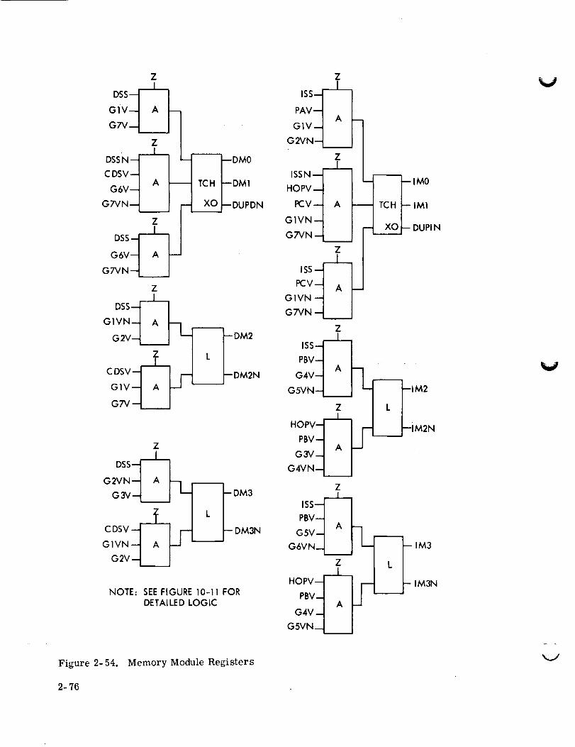
Z
DSS.--_
o,v__I A I-aTv---L.._._
Z
o_s._-__o_o_°_v-l_v-1_Lll '_.._I--°_'GTVN--I___..J_DUPDN
Z
DSS-.J'--L--J
°6v-I " I--G 7VN _....._
7"
DSS
GIVN d A ho_V_z_i, i-o_
Z
DSS--_
1_,w d _ t_ --
G2Y--J___
NOTE: SEE FIGURE 10-11 FORDETAILED LOGIC
Figure 2-54. Memory Module Registers
Z
ISS ---L-I
PAV --
GIV--
G2VN--
ISSN--
HOPV--
PCV-- A J--
GIVN--
G7VN --
Z
ISS --[_
N2V--
GIVN --
G7VN-
Z_A_
ISS--
PBV--
G4V-
G5VN--
IM0
IM!
DUPI N
A_IM2Z
G3V-
G4VN-
Z
ISS_
_v-i II r---n
HOPV'
PBv_|
G4v'-- A L_]
G5VN--L__ I
IM3
IM3N
V
V
2-76

2-178. The latch outputs are combined with the low order bit signal (DM or IM, 0 or 1)from the memory module registers to produce signals IMAVN and BN and DMAVN andBN. These signals are inversions of tratch outputs DM or IM, 0 and 1 at the timesselected by latches RED and REI.
2-179. Memory Module Select Gates. (See figure 2-55.) The two high order bits of themodule selection code are decoded by part of the memory module select gates to produceMZO (module zero or one), MTT (modules 2 or 3), MFF (modules four or five) and MSS(modules six or seven). The outputs of these gates are combined with the timed low-order bits DMAVN, BN and IMAVN, BN to enable the gate-inverters M0 SYN throughM7 SYNC. When these gate-inverters are enabled, they will pass and invert a synchro-nizing signal, SYNCN, to initiate memory module operation.
2-180. Assume that AZOVN is a "1" and that data is to be read in simplex mode. Atphases B and C (essentially), RED will be a "1" and will generate either DMAVN orDMBVN = "0". If DMAVN is a "0", SYNCN will be free to drive MOSYN. If DMBVN isa "0", SYNCN will be free to drive M1SYN.
2-181. In duplex mode, both DMAVN and DMBVN will both be "zeros" in the exampleillustrated; in this case, both MOSYN and M1SYNC will be driven by SYNCN.
2-182. MEMORY SELECT AND ERROR MONITOR. The Memory Select and ErrorMonitor circuit continuously checks the performance of the memory. During duplexoperation, the memory buffer selection is controlled to correct transient errors andprovide an uninterrupted flow of reliable information to the computer. Memory errorsare detected by parity checking the buffer registers after every read cycle and by mon-itoring the outputs of the error detector circuits in the memory modules.
2-183. In duplex operation the A and B memories are cycled simultaneously but onlyone buffer register is selected to provide information to the computer. If an error isdetected during a read cycle, the memory buffer containing good information is selectedto control restoring both memories; thus the error, if transient, is corrected. If anerror occurs in the memory selected to feed the computer, the selection is changed tothe correct buffer before the information is used. Thus the computer receives onlyreliable information unless both memories fail at the same storage location simulta-neously. Operation is not restored to the previously selected memory unless the goodmemory should develop an error. Monitor signals are provided at the computer inter-face which indicate the status of each memory and simultaneous failure of both mem-ories.
2-184. The memory select and error monitor circuit includes separate parity checkand error-detector sensing circuits for each memory; these circuits are called the"error monitors". The error detectors in the memory modules indicate three types ofaddressing failures; 1) multiple address selection; 2) loss of half-select current and3) spurious selection during non-cycle times. These failures are combined into twotypes, "on current failures" and "no current failures" by the error-detector sensingcircuits. Timing signals which enable the error monitors to sense the different typesof errors at the appropriate times are common to both error monitors. The TIMElatch gates outputs from the parity check circuits, and the Check On Current (COC) andCheck No Current (CNC) latches gate their respective typeg of failures, into the monitorcircuits. Outputs of the A and B monitors are combined in the TLC latch to indicatesimultaneous failure of both memories. Memory buffer selection is performed by theMAO-MBO, BRAO and BRBO latches under control of the monitor outputs.
2-77

RED-
DM3N -
DM2-
REI -
IM 3N -
IM2-
RED-
DM3--
DM2N --
REI --
IM3--
IM2N--
°"_1 _ )-I F-m_ m-1' i-"z°
I_ZN-_l '------'
[ A MTT
'_ A MTTNV
A____L_/VlFFVN
RED-- A_
DM3 "- MSS
DM 2
IM3 d /V_SVN
IM2--1
NOTE: SEE FIGURES 10-11, 10-13
AND 10-14 FOR DETAILEDLOGIC.
SYNCN--
DMAVN --
IMAVN--
MZ0VN --
DMBVN --
IMBVN
MZ0VN
DMA VN-
IMAVN--
MTTVN--
DMBVN-
IMBVN -
MTTVN--
DMAVN -
IMAVN --
MOSYN
M 1SYNC
M2SYNC
M_ YNC
_M4SYNC
MFFVN --
V
V
Figure 2-55. Memory Module Select Gates X.F
2-78

RED_
D_VN
DM_VN
A IJ
A
v
IMAVNT,,MBVNI_--T1i I_
X--
PAV
G6V-- A "---7
__7_
G1V
AVN __ REI
x----G5VN--
AVN-- _REI N
X
OP1V--
G4VN
G6V
AV_
_
PBV
G4VN
G6V--
AV--
A
A I--_
i
NOTE: SEE FIGURES 10-12 AND 10-14
FOR DETAILED LOGIC.
_
PAV
G7V--
G5VN--
AVN m
A H
m
G4Vm
AVN_
DMA
[_ DMB
IMB
Figure 2-56. Memory Module Select Control Circuit
2-79

2-185. Parity Check Circuits. Parity checking is implemented in a pair of exclusiveOR "trees", one for each memory buffer. The fourteen bits of each memory buffer areparity checked in parallel and an Error A or B Parity (EAP or EBP) signal generated ifthe fourteen bits contain an even _umber-of "I-'s w'. Figure 2-57 shows the two configura-tions of AND circuits and inverters used to develop the exclusive OR (XOR) function.The circuit shown at A is used when complementary pairs of inputs are available foreach bit. The circuit shown at B is used where only one signal is available for each bit.In either case, output C is a "1" when one and only one input (A or B) is a "1".
Figure 2-57. Exclusive OR (XOR) Circuits
2-186. Figure 2-58 depicts the exclusive OR tree which checks the parity of the A mem-ory buffer. Outputs from the memory buffer are combined into seven pairs, each pairfeeds an exclusive OR circuit at the input to the tree. The output of the exclusive ORrepresents the parity of its inputs. For example, if BRA1 is a "0" and BRA2 is a "1"(the pair has odd parity) then PAO1 is a "1" (also odd parity). The outputs of the ex-clusive OR circuits are then paired to feed the next stage of the exclusive OR tree andcontinue until only two outputs remain; each output representing the parity of half thememory buffed. If the parity of the memory buffer is correct (odd), one of the bits mustbe a "1" and the other bit a "0". The "0" bit disables the input to the PAE6N inverterwhich drives PAE6N to a "1". The bit which is a "1" then enables one of the input ANDsfor the EAP inverter, driving the error signal to a "0".
2-187. Memory Error Monitors. The Memory Error Monitors sense the outputs of theparity check circuits and the error detectors for the A and B memories to determinewhen a failure has occurred. The circuits which are separate for each memory areidentified by an A or B in the names of the output signals. Figure 2-59 shows the errormonitor circuit for the A memory including the circuits which are common for bothmemories. The error signals are developed in four stages. First, the outputs of theerror detectors are sensed and stored in the FSA latch. Second, the set and reset out-puts of the FSA latch are sensed at the appropriate times to detect on-current and no-current failures. A separate check is made for data and instruction modules by theEDAC and EIAC latches, respectively; this provides the timing discrimination necessaryto distinguish normal on-current in one module from a no-current failure in the other,etc. If an error is detected at this stage, it is passed on to the third stage of the mon-itor which senses parity errors. The EADM and EAIM latches are set immediately byan error sensed in the preceding stage or at the proper time if a parity error occurs.
2-80
z0
F
:7
E2F._
z.,o
o.
E_
0
OzQ
u.j "l-
_o
0z
0
_o
i-
d_
/
t
0 0


Z 0
0_o_
d_
Z
_ad4" _, _,,I:=:z
t !
z II._--
I


i_
The "0" outputs of the EADM and EAIM latches are combined in the fourth stage of themonitor (EAM) to indicate an error in either the data or instruction portion of the Amemory. A similar signal (EBM) is developed for the B memory; these signals permitmonitoring the status of each memory individually at the computer interface.
2-188. Another AND-7 inverter circuit combines the outputs of the two second stagelatches EDAC and EIAC, to form the_Error A Current (EAC) signal. A correspondingsignal is developed for the B memory. The TLC latch combines these signals with theoutputs of the two parity check circuits to detect simultaneous failures in both memories.The TLC latch is set by double parity or addressing errors or by the combination of aparity error in one memory and an addressing error in the other. The TLC latch is
reset at the beginning of each computer cycle so that multiple errors may be sensed bycontinuously monitoring the TLC output at the computer interface. A Test EquipmentReset (TER) signal is provided to reset the error monitors; this signaTis returned toU3 VDC when the test equipment is disconnected to provide a continuous "0" input to theRECN inverter. Timing for the COC and CNC latches is keyed to the SYNC signal whichstarts the memory modules to cycle, thereby establishing the time reference for check-ing on current.
2-189. Memory Buffer Select Latches. (Figure 2-60.) From the memory buffer reg-isters information flows in two directions, 1) through the inhibit drivers into the mem-ory and 2) into the computer to be used. The memory select latches provide separatecontrol over data flowing in each direction. The MAO-MBO latch selects the memorybuffer to provide information to the computer and theBRAO and BRBO latches selectthe memory buffer to control the inhibit drivers. Separate control is maintained so thaterrors occurring in the non-selected memory can be corrected from the selected with-out changing the selection of the memory buffer providing information to the computer.
2-190. Operation of the MAO-MBO latch is straightforward. When the error monitorsdetect an error in one memory, the error monitor outputs drive the MAO-MBO latchto select the opposite memory. The latch then remains unchanged until an error issensed from the newly selected memory.
2-191. The outputs of the A and B buffer registers are applied to the inhibit drivers inboth memories so that errors in the A memory can be corrected by inputs from the Bbuffer register and vice versa. The BRAO and BRBO latches gate the inputs from thebuffer registers into the inhibit drivers of the A and B memories, respectively. Assoon as a module in the A memory is selected (DMA or IMA) and cycled without error(EADMN or EAIMN), the BRAO latch is set and remains set until an error is detectedin the A memory. Immediately upon sensing the error the BRAO latch is reset and thecontents of the B buffer register are gated into the inhibit drivers of the A memory tocorrect the error. Operation of the BRBO latch is identical to that for BRAO.
2-83

v
TIME-_
DMB--L____J
TIME_-_
IMB____.J
EAC ._
z- 1TIME-'F_
D_-t_ J
TIME_--] J
NOTE: SEEFIGURES 10-13AND 10-14 FORDETAILED LOGIC
EADMN-_"_
°MA"t-----J J
EAIMN _ _
EAIM_
IMA--J___.J
EBDMN _'-'L_ _
°M_'-I-----JJ
EBIMNW--___4L
EBDM_ BRBO
DMB-I___J1
V
Figure 2-60. Memory Buffer Select Latches
2-84

2-192. DATA CONTROLELEMENT.
2-193. The DataControl Element consistsof the Transfer Register andthe ParityCounter. The transfer register is the central storage location in the computer whichprovides a two-way path for transfer of data or instructions between itself and the mem-ory or itself and other storage locations in the central computer. The p,'u'ity com]terassigns a parity bit to all syllables of data that are stored in the memory. When thesesyllables of data are subsequently read out of memory, their parity condition is checkedagainst the pa.rity bit.
2-194. TRANSFER REGISTER. The Transfer Register is a 13-bit shift register whichreceives from and sends inputs to the Memory Buffer Registers. the Arithmetic Element,
the Multiply-Divide Element, and the external equipment.
2-195. The transfer register consists of 19 latches as shown in figure 2-61. Associatedwith the register are three control latches: SRTN. TBR, and CLTR.
2-196. Serial inputs are applied to the TR1 latch which are shifted bit-by-bit into theregister. The serial inputs are DIN, MD2V, and AI1V. DIN is an input from theexternal equipment. When the external equipment is not supplying an input, DIN may bean open circuit; the input to gate A1 is held to a "0" by V3 (-3 volts). MD2 is an outputof the Automatic HOP Save Circuit which is transferred through gate A2 into the transferregister for storage in the memory. The Accumulator-Register latch, AI1, providestwo serial inputs: the 26-bit data word applied through gate A3, and the eight InstructionCounter bits, A1 through AS, applied through gates A4 and A5. The data word is shiftedinto the transfer register in order to be stored in the memory during ml STO operation(provided the memory address is not 776 or 777, as evidenced by STMDN = "1"). TheInstruction Counter bits are shifted into the register for eventual transfer to the AddressRegister.
2-197. Serial inputs are also applied to latches TRll and TR12 during SHF operationsfrom the AI2 latch of the accumulator-register. (Refer to Arithmetic Element for adescription of the SHF operation. )
2-198. Data is transferred into the transfer register in parallel from Buffer Register Aor Buffer Register B (BRA1 through BRA13 or BRB1 through BRB13) depending uponwhether an odd or even memory is selected. The data is transferred into the correspond-ing transfer register latches TR1 through TR13 at X time, except for those latches(TR2, TR4, TR7, and TRI0) which have data shifted into them at X time. Those latchesare loaded at Y time to avoid a double read-in.
2-199. Shi!ting Data. In a serial shift register, such as the transfer register, theobjective is for each latch to store a given bit for one bit time, then shift its contents tothe next latch in sequence. During the next bit time, the latch stores the bit from thepreceding latch, etc. The type of electronics used in this computer presents certainobstacles to such a register. Data cannot be transferred into a latch until the transferof its contents to the next latch in the sequence is complete. Gating sequential latchesin a shift register at the same time can result in a "rippling" action in which one bitruns the length of the register destroying its contents. To prevent rippling, successive
2-85


i
Z
Z
Z
I I I I t" I I I I I i i t I t
>_>_>_> m
>-
I-iE.-',
i


o
.i
@}


latches in a shift register are gated with a reversed clock sequence. (See figure 2-62.)If latch 2 is gated at X time and latch 3 is gated atWtime, and bit B1 enters latch 2 at2-Xtime. then B1 will not appear in latch3 until 3-W time.
NOTE
Only three clock times separate the gatingtimes between latches.
Subsequent bits will set or reset the latches in a similar manner. A problem occurs atL4. Since L3 is gated at W time, L4 is gated at Z time (the clock time previous to W).However, Z time occurs during the same bit time as W time. Thus. the same bit isgated into L3 and L4 during the same bit time. Since only three clock times separatethe gating of one latch from the other, it becomes apparent that the same data willeventually be available in two latches during the same bit time. The delay latches areinserted into the register to make up for the shortened gating time.
2-200. For timing convenience, the delay latches are gated at Ytime. (See figure 2-61.)Latches TR3DthroughTR12Dare gatedin the order described in the previous paragraph.TR1D cannot be gated at Y time because TR1 is gated at Y time.
2-201. Transfer Register Control Latches. The control latches determine when data isshifted into. through, or out of the register (SRTR). when the register is cleared of data(CLTR). and when data is loaded into the register in parallel (TBR).
2-202. When theSRTRlatch is set, data may be shifted into and through the register ordata in the register may be shifted out through the TRSlatch. GateA94 permits thestored data to be shifted out of the TRS latch starting at B-3-Y time except when TNZ,TMI, TRA, or CDS operations :u'e being performed (TTT = "0"). If a CDS operation isnot being performed (CDSN = "1") and a transfer operation is being performed (TTT = "0").gate A95 permits the stored data to be shifted out of the TRS latch starting at B-5-Y time.
(
NOTE
The operation of the register during an EXMoperation is described later.
During a STO operation, gate A96 permits data to be shifted into the TRS latch startingat B-1-Y time. During a CDS operation (TTT and CDSN ---"0"), gate A97 permits datato be shifted out of the TRSlatch starting at B-14-Ytime. The latch is set at A-7-Ytime of the following computer cycle. During the time the computer is under control ofexternal equipment, RUNVN ="1". WhenOP2 ="1". the latch is reset mad the contentsof the transfer register cannot be shifted out. This condition occurs duringMenmryLoad and Verify operations.
2-203. When the TBRlatch is set. gate A89 permits transfer of the instruction from thebuffer register to the transfer register at A-11-W time; gate A90 permits transfer ofsyllable 0 of the data word and gate A91 permits transfer of syllable 1 of the data wordat B-3-W and C-2-W respectively.
2-88


PHAS[ A
LDI _ II ......
LDI B ' B? 84 _
L5 -- £ B] --
v
BI',,Im
¥ X
¥ X
W
W
Z ¥
Z Y
X
__ .....
X
Figure 2-62. Transfer Register Simplified Block and Timing
2-89

2-204. When the CLTR latch is set, gate A85 controls clearing the transfer register atA-8-Y time prior to read-in of the instruction from the buffer register; at A-14-Y timeby gate A86 prior to data read-in provided a transfer or change data sector operation isnot being performed (TTT = "1"); and when under control of external equipment (RUNVN ="1"), at A-2-Y time by gate A87 in order to prevent stored data from being read intothe address register and an erroneous instruction being performed.
2-205. Operation During EXM. When an EXM operation is being performed, the SRTRlatch remains reset and inhibits shifting data out of the transfer register. The registercan be cleared, except for latches TR5, TR6, TRT, and TR8 the contents of which areretainedbecause EXMVN ="0". The contents of latches TR5 and TR6 are ORed with the
contents of buffer register latches 5 and 6 when the next instruction is transferred intothe register. The contents of latches TR7 and TR8 cannot be altered when the nextinstruction is transferred in the register because gates A41, A42, A46, and A47 areclosed when EXMVN = "0".
2-206. PARITY COUNTER. The Parity Counter assigns parity bits by making allsyllables have "odd" parity. Odd parity means that the total number of "l's" in a syl-lable is odd. The parity counter "counts" the number of "l's" in a syllable and adds a"1", as necessary, so that the total number of "l's" is an odd number. Thus, if thetotal number of "l's" is even, the parity counter adds a bit; if odd, no bit is added. Theparity counter operates during a Store operation when data is loaded into the memory.
2-207. The parity counter consists of three latches: POD, PDD, and PAR, and a con-trol latch, CKP. (See figure 2-63. ) At the beginning of a computer cycle, PAV intializesthe POD latch to the zero (even bit} condition. The PDD latch stores this condition thefollowing W time. During a STO operation, bits are read into the transfer register TR1latch during phase times B and C. (See figure 2-64. ) As syllable zero, bits 25 through13, are shifted out of the TR1 latch into the TR2 latch, the bits are also read into thePOD and PAR latches. The PAR latch is unaffected byinput gates are closed when SBRZ = "0". Since PDD =resets the latch indicating that the total number of bitsneeded. The PDD latch is reset the following W time."1" sets the POD latch indicating that an odd parity bitfifth, etc. "1" resets the POD latch (and the PDD latchfourth, sixth, etc. "1" sets the latch.
bits 25 through 14 because the"1", the first "1" out of TR1is odd and an odd parity bit is notNow PDDN = "1" and the next
is needed. Thus the first, third,subsequently}, while the second,
2-208. When the last bit in syllable zero is read into the TR1 latch, bit 13 at BG14 time,the entire syllable zero is stored in the transfer register. Syllable zero is now ready tobe transferred to the buffer register. This transfer occurs at B-14-Z time when SBRZ ="1" The parity of the low order half of the data must be assigned prior to the transfer.At B-14-W time the PDD latch contains the parity "state" of the first 12 bits of data readinto the POD latch. The TR1 latch contains bit 13 of the data word. These two pieces ofinformation are applied to the set gates of the PAR latch. Two conditions may existwhich necessitate a parity bit to be assigned to the syllable of data: if the number of "l's"in the first 12 bits is even (PDD = "1") and TR1 = "0", thus making the total even; or thenumber of "l's" in the first 12 bits is odd (PDD = "0") and TR1 = "1", also making thetotal even. When SBRZ = "1" both conditions will set the PAR latch and assign a "1" to
the parity bit of the data placed in the memory. At the same time SBRZ will initializethe POD latch to the zero, or even bit, condition. Note that parity is checked anytimedata is shifted into, or out of, the transfer register (SRTR = "1" sets CKP = "1"). How-ever, only a Store operation can set SBRZ = "1".
2-90

cKP
SBRZ-_
SBRZN_-__
cKP--1A I_°°--'1 i
TR1V _.__
SRTR X_
WN_
POD
PODN ___ PDDN
W -...-J
SBRZ_
TRIV--
YN--
NOTE: SEE FIGURE 10-7 FOR DETAILED LOGIC.
Figure 2-63. Parity Counter
2-209. PROGRAM CONTROL ELEMENT.
2-210. The Program Control Element steps the computer program through its instruc-tions to execute the commanded operations. To accomplish this task, the Program
Control Element performs the following functions:
• Starts or stops the program under external control.
• Conditions the memory address decoders to select programmed instructionsor data words.
• Selects data and instruction memory sectors under program control.
• Selects instruction addresses within a memory sector either automatically
or under program control by an instruction counter.
2-91

2-92
o
o
d>w
J
II
._q
. ,,.-I
o
,d
4_
v
V

• Store, decode, and initiate operation codes.
h_terrupt the program, under external control, to perform a selected sub-routine of the program.
Generate a word (HOP constant) which reinitiates the computer program atthe instruction where it was interrupted, after completion of an ex-ternallycorn manded subrout ine.
2-211. The Program Control Element consists of an address register; data and instruc-tion sector registers; operation code register and decoders; interrupt and start-stopcontrol circuits, ,'rod automatic HOP save circuit, and instruction counter. The follow-
ing l)aragraphs describe the operation of the circuits.
2-212. ADDRESS REGISTER. (See figure 2-65.) The Address Register stores instruc-tionor data word addresses while the selected word is read from memory. During aninstruction word time, the address register stores the instruction address (from theinstruction counter) to select the instruction word address; the operand address portionof the instruction word, stored during data word time, is used to select the data word
address.
2-213. The address register consists of nine latches, AI through A9, with associatedAND m_d INVERTER output circuits for added driving power. Latches A1 through A8select one of the 256 memory locations in a sector; latch A9 determines whether theaddressed data will come from a pre-selected sector, or from the residual memory.The addresses of selected memory locations are loaded into the address register from
the transfer register. The address register outputs condition the address decoders inthe Memory Control Element and provide control to the data adapter for PlO operations.The transfer address (TA) latch provides timing and control for the register.
2-214. The instruction address (from the instruction counter) is stored in the address
register from A-8-Wthrough A-13-Xtime. (See figure 2-66.) During this period, theaddressed instruction is read from memory and placed in the transfer register. Theoperand address portion of the instruction is then transferred to the address register atA-13-Ztime for storage while the data word is read from memory. The address registerstores the data word address from A-14-W through the foltowingA-7-Xtime. The ad-
dress register is reset at A-7-YandA-13-Ytimes. prior to stormgthe instruction anddata addresses.
2-215. The TA latch is set during two different periods. The TA latch is set fromA-7-X to A-8-W time, during this period the address register is reset at A-7-Y timem_d is loaded with the instruction address at the following Z clock time. The TA latch
is set again from A-13-X to A-14-W time; at this time the address register is reset atA-13-Y time and is loaded with the data word address at the following Z clock time.
Operation of the TA latch and address register differ slightly during an execute modified(EXM) instruction.
2-216. An EXM instruction executes,'md modifies theoperand address of one of theinstructions stored in residual memory locations 600, 640, 700, and 740. Theoperandaddress portion of the EXM instruction is transferred into the address register at A-13-Ztime. The data stored mlatches A1 throughA5 remains in the transfer register to
select the syllable of the instruction to be executed and modify its address, but this datamust be cleared from latches A1 through A5 to select the desired residual memorylocat ions.
2-93


Z Z
I
r_] _1 I_'1X
_, LI
7_ d--<Z@
_Z_
0Z
I
I I I I x I I I I I
.4[
I
1Z
E


ZO
O¢
O
xI.U
NORMAL
OPERATION
EXM
EXECUTE
INSTRUCTION
EXECUTE
WXYZ
ITflI
BIT
CLOCKS
PA
AVN
GI
G5N
G6
G7
TA
A(I -9)*
7
EXM
A(1-5)* i
TA
EXM
Aft -5)* iA(6-9)*
"I"LEVEL "O"LEVEL I_ AMBIGUOUS OR SWITCHING TIME
* SET WHEN TR (I -9) EQUALS "I" AT A-7-Z OR A-I 3-Z
Figure 2-66. Address Register Timing
2-217. Address register latches A1 through A5 are reset at B-1-Y time to selectaddress 600, 640, 700 or 740. Since the address register already contains the address
of the next instruction at A-7-Z time, TA equals "0" to prevent the instruction addressfrom the instruction counter from being loaded into the address register; the EXMNlevel equals "0" preventing the TA latch from being set. The address portion of the
instruction to be executed, already modified in the transfer register, is loaded into theaddress register at A-13-Z time. The address modifying bits A-1 through A-4 of the
EXM instruction had remained unchanged in the transfer register during phase B and Ctimes of the EXM instruction because memory operation was halted. After the address
portion of the instruction to be executed is loaded into the address register the computer
resumes normal operation.
2-218. DATA AND INSTRUCTION SECTOR REGISTERS. (See figure 2-67.) The Data
and Instruction Sector Registers store sector codes to select one of 16 mem_'y sectorsduring operation and instruction times, respectively. Sector codes are loaded into both
registers during a HOP instruction (HOP sets CDSV to load the data sector register);the data sector register is also loaded during a change data sector (CDS) instruction.The registers store the sector codes until the next HOP (or CDS) instruction commands
them to change. The sector register outputs condition the memory address decoders.
2-95

G3VN---_
°_--L--J I L I
G6VN -_ _
G_V--1_ M I-°s_o_s.--_I ,_I
C DSV_
G1VN--_
G2V--I. I r----1
pB,,_l_ r-I i--,_
GlVq II
HOPV _.,___J
HOPV ISS
TRSV'--L"___,_
G4VN --_
Gsvd A H I-°s_,:,ss-L._lI,-I
G3V,,,__I-_°s2"G4V--I" I-'
CDSV"_, J
G6V--_
P_V-1 I ,slISS_
_ISN
G_V_-IA U
HOPV--____]
G 2VN-_
°'v_-I II
P_V_ IHOPV_
GSVN-_
G6V--I_ I--I I-°s_°SS-L-_ I _ I
G1V-_
A
G_Vq II
PBV--I IHOPV_
v@h- 7_C DSV DSS
i IL._--DSS N
WN
BRA8-_ BRA7--_
Ex"'v---IA L. _xMv-I,,I__°v-I II '_°v-I II,.v___jI '"v--L_I
EXMV---I _ I I c----n EXMVM . I I r-----n
MBOV.---.I '_ _ F DS|M MBOV t _ F DS2M
_.v--_ i,i ,.v-L_j iLl
NOTE: REFER TO FIGURE 10-17 FOR
DETAILED LOGIC.
V
Figure 2-67. Sector Registers and Control Latches
2-96

2-219. The datasector (DS)andinstruction sector (IS) registers eachcontainfourlatches. The DSregister is loadedby the datasector serialized (DSS)latch; likewise,the IS register is loadedby the instruction sector serialized (ISS)latch. The datasectorselection is altered for onecomputercycle following an executemodify (EXM)command.During the executionof an instruction following anEXM command,the two datasectormodified latches (DS1MandDS2M)substitute for the DS1andDS2latches to conditionthememory addressdecoders. The HOPconstantappearsas a 26-bit serial outputof thetransfer register serializer latch (TRS)during phasetimes B andC. The datasectorcodeoccupiesbits 2 through5 andthe instruction sector codebits 20 through23of theHOPconstant. The DSregister canalso be loadedfrom operandaddressbits A5 throughA8 of a CDS instruction. The transfer register produces the data sector code at TRSduring the same bit times for both HOP and CDS.
2-220. The DSS latch is gated to duplicate the TRS output during phase C. The datasector code emerges from the DSS latch at bit times C-10 through C-13. (See figure 2-68. )The set gates of latches DS1 through DS4 bear the timing signals which sense DSS at theproper times to gate each bit of the data sector code into the appropriate latch. Eachlatch is reset one bit time before sensing DSS, clearing the previous code before the newcode is loaded.
2-221. The IS register is loaded in the same manner as the DS register with the follow-ing exceptions. The IS register is loaded only during a HOP command and therefore, itsreset gates are enabled by HOP rather than CDS. The instruction sector code occupies adifferent position in the HOP constant than the data sector code and consequently requiresdifferent timing signals to accept it. The IS register is loaded at bit times B-6-Z throughB-9-Z.
2-222. The data sector modified (DS1M & DS2M) latches are substituted for the DS1 andDS2 latches during the operation time of the instruction following an EXM command.From A-11-Y to the following A-6-Y time, the DSM latches store operand bits A1 and A2of the instruction to be executed; the MAOV or MBOV, TBRV, and EXMV signals permitloading the DSM latches at A-11-Y time. The A1 and A2 bits are loaded into the DSMlatches from the selected memory buffer.
2-223. During the execution of the operation following an EXM instruction, the datasector code substituted for the DS register outputs is as follows: The DSM latch outputssubstitute for DS1 and DS2 latch outputs; the EXMD latch output substitutes for the DS3latch output; and the A9 bit of the instruction to be executed substitutes for the DS4 latchoutput. See figure 2-6 for a brief account of EXM operation.
2-224. OPERATION CODE REGISTER. (See figure 2-69.) The four bit Operation (OP)Code Register stores the code of the commanded instruction while the instruction isexecuted. The OP code register outputs control the operation of the circuits whichexecute the instructions.
2-225. The OP code register, loaded by the transfer register, stores the operationcode from A-12-Y to A-5-Y time, nearly a full computer cycle. See figure 2-70 for theOP code register load and reset conditions. Operation of the register differs slightlyduring a multiply and hold (MPH) operation and during computer single step operation.
2-97

2-98
J
w
|
b_
-,-4
(D
0
C.)
o-r-I
od
!
g.,-..t

II
>" I I I Iz_o0 _-
Zl_. Q..
0 0
I I
I
I IIoz_
0
I ?
>- I i I I >-
0 0 u
Z
0 0
I I
I,u
I
I I I I I I I
0 0
d
0._1
r_iii._,1
Iii
0ii
iiii11
I
O0!
0
iii
011
0
i11ii
iii
0Z
Z
0 0I I
..J
II
I?I I I I I I I
0 _ 0
a.
0
l
Z
0
I
I
>- I I I I I I Ie_l it)
0 _- 0
0
0
0
I
0
,,-I
2-99

%d
PHASE A 8
I"'"LEVELnII"o"LEVEL I_AMBIGUOUS OR SWITCHING TIME
* SET WHEN TR(10-13) EQUALS "I" AT A-12-Y
Figure 2-70. Operation Code Register Timing
2-226. At the completion of an MPH operation, the force clear and add (FCD) signalenables transfer of tile contents of the PQ register into the accumulator. The FCD
signal forces a clear ,rind add (CLA) operation code into the OP code register and selectsthe PQ register as the data address. The MPH operation code is loaded into the OP code
register, as per normal operation, during the first computer cycle (MPH requires five
computer cycles). During the second computer cycle of an MPH operation, FCD equals"0" at A-1-Y time to set the OP code register to all "l's" (CLA). The product of tile
MPH operation, located in the PQ register, is not transferred into the accumulator
until the fifth computer cycle. The CLA code is cleared from the OP code register atA-5-Y time of the next instruction, six computer cycles after initiation of the MPH
operation.
2-227. Computer single step (CST) operation is used to step through selected instruc-tions, one at a time, on command. The externally controlled CST signal, enabled duringphase C time of the selected instruction, forces a transfer non-zero (TNZ) operation
code into the OP code register. The TNZ operation code disables memory because it
requires no operand. The OP code register is reset at A-5-Y time, as per normaloperation; then the OP3 latch is set at A-6-Y time (PA, G6, G7N, CST equal "1") forcingthe TNZ operation code (0100) into the OP code register. The TNZ code is loaded at
A-6-Y time to disable the memory prior to instruction read time, thus preventing a new
operation code from being loaded into the OD code register at A-12-Y time. The com-
puter then idles in this condition until the externally controlled CST gate is momentarilydisabled allowing the next operation code to be loaded into the OP code register at normalload time.
2-100

k__#
2-228. OPERATIONDECODERS. (Seefigure 2-71.) The OperationDecoderssupple-ment the OP coderegister in controlling the operation of circuits which executethecommandedoperations. Theoperation decodersdecodeprogrammedoperation codesandcomputer signal combinationsto generatecontrol signals. Theporgrammedopera-tion codeswhich conditionthe decodersare suppliedvia the transfer register, addressregister, or OP coderegister. Theoperation decodersare listed below in alphabeticalorder:
• ChangeDataSectorLatch
• ExecuteModifiedandExecuteModified DelayedLatches
• HOPLatch
• Process Input OutputGate
• Shift AndPIO Gate
• Shift Gate
• SSGate
• SSFGate
• Store AndStore Not Gates
• TTL Latch
• TTT Gate
2-229. Change Data Sector (CDS) Latch. During CDS and HOP operations, the CDS
latch permits the data sector register to store the data sector code. The CDS latch
also initiates shifting the contents of the transfer register out to the TRS latch during aHOP operation.
2-230. During a CDS operation, the CDS latch is set from A-14-W through B-5-Y time
and from B-13-W through A-5-Y time. The CDS latch is set by the CDS operation codestored in the transfer register. The shift right transfer register not (SRTRN) signalequals "0" during transfer register shift operation to prevent the CDS latch from beingset by a false CD6 code.
2-231. During a HOP operation, HOPV sets the CDS latch at C-1-Z time; the CDS latch
remains set from C-2-W through A-5-Y time.
2-232. Execute Modified (EXM) and Execute Modified Delayed (EXMD) Latches. TheEXM latch is set from B-14-W through A-13-Y during an EXM operation. The EXM
latch is set by the EXM operation code via the OP code and address registers. The EXMlatch enables the EXM operand address bit A5 to select the syllable of the instruction to
be executed and clears address register latches A1 through A5 to select one of fourresidual memory locations. During phase A time of the instruction following an EXM
command, the EXM latch enables loading of the data sector modified latches.
v
2-101

i
G5VN--
TR1V--
TR2V--
TR3V--
TR4V-- A
TRSV--
TR6V--
TR8V--
TR9V--
STOVN -- A
NOTE: REFER TO FIGURES 10-6, 10-7, 10-8 (SHEETS 1 AND 2),
10-15, 10-18, 10-20 (SHEET 1), 10-21 (SHEET 2), AND
10-35 (SHEET 3) FOR DETAILED LOGIC,
SSF
STO
OPI _ _ STON
72q4-r TOV.o_.- I I L__JOP4V_
V
¥Z3_G6V--
PAV-- A
SSF--
G5V--i •
G6VN--i A
PAV--
TTLV
OPIVN'--_
oP2v.-I A r-I
OP4V_----_ I
OPIVN--J-- 1 .
OP2VN--I A
oP_,_
TTT
Figure 2-71. Operation Decoders (Sheet 1 of 2)%.,'
2-102
_._J!
A
EXM
EXMV
SAPO

2-233. The EXMD latch is set by the EXM and transfer address (TA) signals at the end
of an EXM operation. The EXMD latch is set from A-13-Z through A-7-X time. The
EXMD latch conditions the memory address decoders to modify data sector selection
during execution time of the instruction following an EXM command.
2-234. Force Clear and Add (FCD) Gate. FCD forces a CLA operation code into theOP code register during phase A of the second through fifth computer cycles of a multiply
and hold (MPH) operation. (Signals HOYV and VOYVN equal "1" during an MPH opera-
tion. ) FCD also initiates transfer of the contents of the P-Q register to the accumulator
by setting the TTL latch.
2-235. HOP Latch. The HOP latch, set from A-13-W through A-6-Y time during an
HOP operation, initiates loading of the instruction and data sector codes into their respec-
tive registers, disables memory, and conditions module current error latches in theMemory Control Element. The HOP latch is set by the HOP operation code stored in the
OP code register.
2-236. Process Input Output (PIO) Gate. PIO equals "1" during the period that a PIOoperation code is stored in the OP code register. (Input signals OP3V and SAPO equal
"0". ) The PIO signal conditions the accumulator to accept external data when commanded
by the PIO instruction.
2-237. Shift And PIO (SAPO) Gate. SAPO equals "0" when CDS, EXM, PIO, and SHF
operation codes are stored in the OP code register. The SAPO signal conditions thePIO and SHF decoders.
2-238. Shift (SHF) Gate. SHF equals "0" when a SHF operation code is stored in the OPcode and address registers. The SHF signal is applied to the Arithmetic Element and
transfer register to control the shift operation.
2-239. SS Gate. SS equals "1" from A-8-Y through B-I-W time when the transfer
register stores an operand address of 776 or 777. Normally, during an interrupt opera-tion a programmed STO 776 or 777 instruction will be given to store the automatic HOPconstruct in one of these locations. SS initiates transfer of the automatic HOP constant
to the transfer register for storage in memory.
2-240. SSF Gate. When the transfer register contains operand address 775, SSF equals"1" from A-12-Y through B-I-W time. The operand address is cleared from the transfer
register at B-1-X time during non-transfer operations. SSF initiates transfer of theP-Q register to the accumulator or vice versa.
2-241. Store (STO) And Store Not (STON) Gates. The STO and STON gates are condi-
tioned when a store operation code is stored in the OP code register. The STO gateinverts the STOVN signal to generate a STO signal. The STO and STON signals initiatetransfer of the accumulator into the transfer register; then initiates parallel transfer of
the contents of the transfer register into the buffer register for storage in the memory
address specified by the operand address of the store instruction.
2-242. TTL Latch. The TTL latch is set by the SSF signal to initiate transfer of the
P-Q register to the accumuIator or vice versa. The TTL latch is set from A-12-Z
through A-5-X time.
V
%.J
2- 104

_J2-243. TTT Gate. TTT inhibits clearing and shifting of the transfer register during
transfer (TNZ, TMI, and TRA), CDS and HOP operations. The TTT signal equals "0"while transfer operation codes are stored in the OP code register or while the CDSlatch is set.
2-244. INTERRUPT CONTROL. (See figure 2-72.) The Interrupt Control, on external
command, stores the interrupt command (INTCV) until completion of the current instruc-tion under execution, then halts the computer program and initiates a HOP to memorylocation 400.
2-245. The interrupt control consists of three latches; the INTA, INTB, and INT. The
INTA latch delays initiation of the interrupt command if the computer is executing in-structions requiring multiple computer cycles. These instructions are multiply (MPY),
multiply and hold (MPH), divide (DIV), execute modified (EXM), and HOP. The INTBlatch insures initiation of only one interrupt operation per interrupt command. The
INT latch halts the computer program and initiates the HOP to 400.
2-246. At the first X clock time following the interrupt command (INTCV = "1") the
INTA latch is set providing HOYVN, VOYVN, HOPN, EXMN, and INTBN equal "1"The HOYVN and VOYVN signals equal "1" during non-execution periods of MPY, MPH,
or DIV operations. The condition when INTBN equals "1" indicates that the currentinterrupt has not yet been initiated. Once set, the INTA latch resets at the following Wclock time.
_...J
2-247. The INTA signal sets the INT latch at A-1-Y time; INT resets at the following
A-11-Y time. Excluding the exceptions already noted, instructions require approximatelyone computer cycle to execute; consequently the INT latch can be set at A-1-Y time
without interrupting the execution of an instruction. During its set period, the INT latchinitiates a HOP to 400. The INT signal also sets the INTB latch to prevent initiating
additional interrupts until completion of the interrupt operation. At the completion of aninterrupt operation the INTCV signal is reset. When INTCV resets, the INTB latch alsoresets.
2-248. START-STOP CONTROL. (See figure 2-73.) The computer program start-
stop operation is controlled by two externally provided signals; HALTV and CSTN. The
HALTV signal conditions the Run Latch to control the computer program start-stopoperation during normal operation. The CST signal conditions the CST gate to controlcomputer program start-stop operation during computer single step operation.
2- 249. Run Latch. The Run Latch is set each A-6-Y time and remains set until the
computer is externally commanded to halt; then HALTV equals "1" resetting the runlatch at A-6-Z time. During the periods that the run latch is set the computer is
permitted to operate as programmed. The computer program is initiated when the runlatch becomes set by a simulated HOP to 000 instruction since the syllable latch, module,
sector, OP code, and address registers contain "O's". A HOP constant will be storedin memory location 000 to start the computer program.
2-250. When the run latch is reset the computer program is halted in the followingmanner. The run latch disables memory during phase A, consequently instruction
words cannot be read from memory. The transfer register and in turn the OP code and
address registers will be loaded with "O's"; thus commanding a HOP to 000. When theHOP code is loaded into the OP code register the HOP latch becomes set. When bothHOP and RUNVN equal "1" memory operation is also disabled during phases B and C.
The reset run latch prevents the transfer of the instruction address into the transfer
register; consequently the HOP to 000 command is continuously recycled.
2-105

X2---jI NTCV--
EXMN--
HOPN-- A _ INTAHOYVN- ILlVOYVN- j
INTBN- _ [_ INTAN
WN
w6--1-INT-- A I--
INTCV
Figure 2-72.
G2VN --
PAV-- A
PBVN--INTA-- _ j--- I,_NT
- iv6Z___
G4VN-- A _ I--'- INTNG5Y--
NOTE: REFER TO FIGURE 10-8 (SHEET I) AND
10-21 (SHEET 2) FOR DETAILED LOGIC
Interrupt Control
2-106

¥-qG6V_
_AV-L--Jkn
RUN
RUNV
RUNVNG7VN-- 1 ,
PAV d
HALTV--.L_
CSTN-__ CSTV
NOTE: REFER TO FIGURES 10-13 (SHEET I) AND 10-30(SHEET 2) FOR DETAILED LOGIC.
Figure 2-73. Start-Stop Control
2-107
2-251. In addition to halting the computer program the reset run latch initializes themultiply or divide phase counter to the quiescent state and prevents the accumulator andautomatic HOP constant from being transferred into the transfer register. During theperiod that RUNVN and HOP equal "1" the module current error latches are reset forinitialization. The RUNVN signal also enables the transfer register to be loaded fromexternal sources via the DIN line. The DIN line is used during a memory load or verifyoperation.
_-2-252. During memory loading or verification, CLA and STO commands are loaded intothe transfer register during instruction time via the DIN line. During execution of theseinstructions memory operation is enabled during phases B and C but remains disabledduring phase A. During data word time of STO commands, data is loaded into the transferregister via the DIN line for storage in memory. The RUNVN signal clears the transferregister at the completion of these commanded operations.
2-253. CST Gate. The CST gate inverts the externally provided CSTN signal to halt thecomputer program during single step operation. The CST signal forces a transfer nonzero (TNZ) operation code into the OP code register, prevents the instruction counterfrom stepping, and prevents the operand address from transferring from the transferregister into the instruction counter if the accumulator contains a non-zero number.Since the instruction counter is unable to increase and transfer is inhibited, the TNZoperation is continuously repeated halting the computer program. When the CST gate isdisabled the next programmed instruction is performed.
2-254. AUTOMATIC HOP SAVE CIRCUIT. The Automatic HOP Save Circuit assemblesa HOP constant; stores the HOP constant for approximately one computer cycle (exceptduring multiply or divide operations); and when commanded by the computer programenables the transfer register to accept the HOP constant for storage in memory. Theautomatic HOP constant will not be stored in memory unless a store instruction is givenwith an address of 776 or 777. The automatic HOP save circuit consists of a HOP
constant serializer, delay circuits (located in the Multiply- Divide Element), and a con-trol circuit (STMD latch).
2-255. The HOP constant serializer assembles a partial HOP constant every computercycle. The instruction address (from the instruction counter) is merged into the HOPconstant during a transfer operation. The HOP constant is shifted through the delaycircuits (multiplicand-divisor register) for approximately one computer cycle duringoperations other than multiply or divide. The STMD latch, under program control,enables the HOP constant to be shifted into the transfer register for storage in memory.
2-256. HOP Constant Serializer. (See figure 2-74.) The HOP constant serializerassembles the portion of the HOP constant which contains the syllable code (SYLCIV),the instruction and data module codes (IM and DM), the instruction and data sector codes(IS and DS), and the simplex-duplex codes. The HOP constant serializer also assemblesthe data sector modified codes (DS1M and DS2M) to enable monitoring DS1M and DS2Moperation during testing. The DS1M and DS2M codes are circulated through the delaycircuits but are miss-timed for storage in memory. The HOP constant serializer outputis loaded into channel one of DL31. :
2- 257. The HOP constant serializer consists of three latches, OC, HPl, and HOPC1.The OC and HPl latches serialize data during even and odd bit times, respectively. TheHOPC1 latch merges the OC and HPl outputs.
V
V
2-108

G4VN
_Bv-I II'_'_ Io,v-_ I
G6v"-I A
_:vq_j-G1V'-_
G6v--1 ,_.v-1 I
iS3--_J
_Y'_'V-L.__JI
o,v- IG_YN--1 II
oMI--L__j J
G6v-1,_I-4
°__
°___v
1_3
INI0
AV_ HP! N
GSVN
PBv-I !IM3 _._J
GTVN
IS2
G7V
PIV
Is4--k___l J
G_N
DM1
oUeON--L__JI
G7V
DM3
:::L_J[
G6v-I A
°'v"-I . I1
ou_N--L_.J J NOTE:
O_VN--I _
AVN __- OCN
HP1
O_ I-K_PCIV
C__-- HOPC IN
XN
,REFERTO FIGURE 10-12FOR DETAILED LOGIC
Figure 2-74. HOP Constant Serializer
Changed 4 January 1965 2-109

2-258. The OClatch canbe set during selectedevenbit times; the selectedbit timesare A-14, B-4, B-6, B-8, C-6, C-8, C-10, C-12 andC-14. (Seefigure 2-75.) TheHP1 latch canbe set during selectedoddbit times; the selectedbit times are A-13, B-3,B-5, B-7, B-9, C-5, C-7, C-9, C-11 andC-13. The OCandHP1 latches reset duringodd-X andeven-X times, respectively. The HOPC1latch is alternately loadedwith theodd andevendataoutputsof the OCandHP1latches. The HOPC1latch resets at Xclock times prior to being loadedwith the nextbit. The HOPC1latch serialized outputis loadedinto channeloneof DL31.
2-259. Delay Circuits. The Delay Circuits circulate the HOP constant for approximatelyone computer cycle during non-multiply-divide operations. The delay circuits are loadedserially from both the HOP constant serializer and the instruction counter. The HOPserializer data is loaded unconditionally every computer cycle but the instruction portionof the HOP constant is only loaded during three operations; transfer, HOP, or interrupt.During an interrupt operation a HOP instruction is forced to enable the instruction ad-dress to be loaded into the delay circuits. The HOPCIV gate loads the HOP constantserializer into the delay circuit, whereas the instruction address is loaded into the delaycircuit from the ACC0 latch.
2-260. The delay circuits consist of channel one of two delay lines (DL31 and DL44),four latches, and associated AND gates. (See figure 2-76. ) The four latches are: NU,MD0, MD1, and MD2. The delay circuits are serially connected as shown in figure2-76.
2-261. The DL31 delay line stores the HOP constant for 15 bit times plus 2 clock times.DL31 is loaded at W clock time (channel one) by the HOPC1 and ACC0 latches. UTRequals "0" from B-10-Z through C-4-X time during transfer_operations to enable loadingthe instruction address via the ACC0 latch. The channel one output of DL31 is loadedinto the NU latch at Y clock times. See figure 2-75 for delay circuit timing.
2-262. The DL44 delay line stores the HOP constant for 22 bit times plus a clock time.DL44 is loaded by the NU latch at W clock times (channel one); HOYN and VOYN equal"1" during non-multiply - divide operations. The channel one output of DL44 is loadedinto the MD0 latch at X clock times.
2-263. The MD1 and MD2 latches provide a delay of two bit times from the time MD0 isloaded until the transfer register is loaded. The MD1 and MD2 latches sequentially loadthe HOP constant at Z and Y clock times, respectively, following the loading of MD0 atX clock time. When enabled, MD2 loads transfer register bit one (TR1) at X clock timesof bit times B-2 through C-13. STMD, SRTR, and RUNV all equal "1" from B-I-Zthrough C-13-Y time during a store 776 or 777 instruction.
2-264. STMD Latch. (See figure 2-77.) During a store 776 or 777 instruction, whichis normally commanded during an interrupt operation, the STMD latch is set to enablethe transfer register to store the automatic HOP constant. The STMD latch is set,when enabled by STO and SS, from B-I-W through C-13-Y time. See figure 2-75 forSTMD timing.
2-265. INSTRUCTION COUNTER. The instruction address is incremented in theArithmetic Element and stored in the unused portion of the accumulator register. Theinstruction address consists of nine bits but only eight bits are stored in the accumulatorregister. When the instruction address is transferred to the address register from theaccumulator register to select an instruction, a "0" is forced into address register bit
V
%J
2-110

z
---- T
C-
i
J
wJ
:o
D
|
b_
.,.=_
H.,.=#
.,.._
.,-4
O
0
_4
!
2-111

HOPCIV__ A DL31
×N
NU
NUN
To Other Gates
HOYN
VOYN--I_.__]ItI
To Other Gates
DL44
WN
To Other Gates
Z_ I Y_ FMD2
MDO _
MDON_MD2N
I¢
To Other Gates
X_
M°2vF-}STMD d To
SRTRd
RUNV--L_
NOTE: REFER TO FIGURES 10-3, 10-4
(SHEETS 1AND 2), 10-5
TR1
(SHEETS 1 AND 2), AND 10-28(SHEET 2) FOR DETAILED LOGIC.
Figure 2-76. Delay Circuitsk.)
2-112
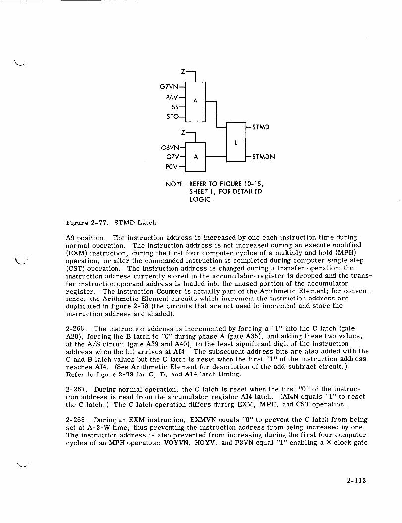
_
NOTE: REFER TO FIGURE 10-15,
SHEET 1, FOR DETAILEDLOGIC.
Figure 2-77. STMD Latch
A9 position. The instruction address is increased by one each instruction time during
normal operation. The instruction address is not increased during an execute modified(EXM) instruction, during the first four computer cycles of a multiply and hold (MPH)
operation, or after the commanded instruction is completed during computer single step(CST) operation. The instruction address is changed during a transfer operation; the
instruction address currently stored in the accumulator-register is dropped and the trans-fer instruction operand address is loaded into the unused portion of the accumulator
register. The Instruction Counter is actually part of the Arithmetic Element; for conven-ience, the Arithmetic Element circuits which increment the instruction address are
duplicated in figure 2-78 (the circuits that are not used to increment and store theinstruction address are shaded).
2-266. The instruction address is incremented by forcing a "1" into the C latch (gateA20), forcing the B latch to "0" during phase A (gate A35), and adding these two values,
at the A/S circuit (gate A39 and A40), to the least significant digit of the instructionaddress when the bit arrives at AI4. The subsequent address bits are also added with theC and B latch values but the C latch is reset when the first "1" of the instruction address
reaches AI4. (See Arithmetic Element for description of the add-subtract circuit. )
Refer to figure 2-79 for C, B, and A14 latch timing.
2-267. During normal operation, the C latch is reset when the first "0" of the instruc-tion address is read from the accumulator register AI4 latch. (AI4N equals "1" to resetthe C latch. ) The C latch operation differs during EXM, MPH, and CST operation.
2-268. During an EXM instruction, EXMVN equals "0" to prevent the C latch from being
set at A-2-W time, thus preventing the instruction address from being increased by one.The instruction address is also prevented from increasing during the first four computer
cycles of an MPH operation; VOYVN, HOYV, and P3VN equal "1" enabling a X clock gate
2-113

I
GIVN--i!!i!i!i!i!!!!!i!i!_!i!
:::::::::--::::::::
PCv _ !!!!!!!!!!!_!!!T!]!!!!!_ 16_
l SHFV_i!i!i#!!_!i!i!ii!i!i!i!i::::::::::::::::::::::
A1V--_ii!i!i!i!i!i!i!i!i!i!i!::::::::::::::::::::::
I AI3V--: ......................
X --
I --G5VN- i!i!!!i!i!i!iiii!i!i!=====================
G_- iliiiiiiiiiiiiiii!iliJ AVN-- iiiiiiiiiiiiiiiiiii!
_V -iiA 17_
I _H_V-iiiii!iiiiiiiiiiiiii:+:.:.:.:.:+:+:
i A2V- i_i_i;iiiiiiiiii_iiiiAI IV'- i!iiiii_i!i!!_i_i_i!il
IIIII ,oY_ A,8•l P3VN_ JI
G3VN
I
III
AISw.-- I
GIV_
G3VN I
PAV_ A20
Z--
O P3V _ ........................:::::::::::::::::::::::::
TE Vi ii::_A 21 :::
RA C N -- ...................:_i
..:......:.....
e N " ::::::::::::::::::::::::::::::::::::
z_
OP3VN --,-__
Z_
o,,,v_i!:!i_i_O P2V --,i :::::::::::::::::::::::::::::::::
| ::_'A23_::
Z_
o_,v-_OP2V--
' i_A24!AI4N _ ......
BN_
z__AVN--I:::::::::::::::::
I ::!::i:A25 ::i
z_o _ N_ i_,,ii!ii_,i!_iA_4N_ i::X;_61!i
z_
PAV I A27
AI4N-I__
NOTE:
X_
T_C-I;!;!;!;!;!_;!;!!!;!Tl"l.V-Iiiii_A28
::::::::::::
QBD - f!i!i!;!i_!;_!i!i!i!!
W--
PAVN --I;i_i_i_i_i_i_i_i_i_
SHFV-- !!_!_!_!!!!!_!!!!!_!i!!
A IV-- :::::::::::::::::::::::
AI2V-- i:_:_:!:!:!:!:!:_3!:!
w_TBCV -- i_!_i_ii_i_i_i!ii!_
_:_:!:!:!:!:_:!:!:!:i:iPIOV --_!_!_!_!_!_!_!_!_
A2V-iiiil;i;iliiiiiiii!iDATAv_iiiiiiiiii!;il;;ii!ill
TRSV _ _:_:_:_:_:;:_:_:j_,_
w_
z_
o_,v_x_
G2VN -- _;_:::::::::::::::::::::.:+:.:-:.:.:-:.:.:.
GTvN- !i!iiiiiiiiiiii)ilili!$!:!:!:!:!Si:i:i
P_VN-- ;i;i!iiiililililiiii.:.:.:.:.:.:.:.:.:.:.
Ev- IA:_IAVN-- i_!_!!!!
ililiiiiiiiiiiiii!iSHFV-- ..........:::::::::::::::::::::
AIV--
z,--__
REFER TO FIGURE 10-.5 SHEET I, FOR DETAILED LOGIC. ., ,
Figure 2-78. Instruction Counter (Sheet 1 of 2) L2
2-114

(3w
cE
:>
o=
oS-Z3:
Z
*_l--r
Ul_ ___ _ _ _ _ U
_11×1> > oov_ UUI_ _ uu
o__--]u
_ i
® ® °°°°
.@.@
_ _ Z
I_-_2LI....
o
9u
oz
0
u_
Ii


__i__........._!_I-
m _ ._ _._ .......
i._=__
• : i !
L L ......m
I J )
r
I
I _R= i
--_ ___-_ ........
[]
m
.,,..4
,,--4
q}
o
2-116


to repeatedlyreset the C latch. During the MPHfifth computer cycle P3VNequals "0"permitting the C latch to remain set after A-2-W time to increase the instruction addressby one. The instruction address is also preventedfrom increasing during a CST opera-tion while CST equals "1". The C latch is repeatedly reset at A-2-W time when CSTequals "1" to keep the instruction address from increasing. To select the next program-med instruction during CST operation the externally controlled CST level becomes a "0"momentarily to allow the instruction address to increase by one.
2-269. The accumulator register stores the instruction address after the results of thearithmetic computations. The accumulator circulates the instruction address in thesame manner that the arithmetic computations are circulated. The instruction addressis loaded into the accumulator automatically by the add circuit and also, during transferoperations, by the transfer register serializer (TRSV). The accumulator also suppliesthe transfer register with the instruction address to select programmed instructions.
2-270. During a transfer operation, the transfer instruction operand address is serializedthrough the transfer register and TRSV latch to load ACC1 of the accumulator register.During this period, UTRV equals "1" and UACCO equals "0" to enable TRSV to load thenew instruction address and inhibit the currently stored instruction address at ACCO.The UTRV and UACCO levels originate at the same latch so can never equal "1" simul-
taneously. UACCO equals "1" during non-transfer operations to enable the currentinstruction address to be circulated through the accumulator. The AI1 latch of theaccumulator register sequentially loads the TR1 latch of the transfer register with theinstruction address during bit times C-14 through A-7. The instruction address, whilestored in the transfer register, selects the next programmed instruction.
2-271. ARITHMETIC ELEMENT.
2-272. The Arithmetic Element performs the following general type of operations:
a. Arithmetic (addition, subtraction and shifting).
b. Logical extraction.
c. Stores new operand and a new instruction counter (previously described).
d. Modifies the stored instruction counter.
2-273. The Arithmetic Element consists of the following (figure 2-80):
a. Accumulator Control Circuits (Accum Control)
b. Add/Subtract Circuit (A/S)
c. Accumulator Register (Acc Reg)
The A/S Circuit and Acc Reg make up an accumulator which performs the arithmeticand logic operations and stores the results. The Acc Reg stores two pieces of data:results of the arithmetic operation, called the stored operand, and the instructioncounter.
the
2-274. The Accum Control Circuits provide timing and conditioning gates for the A/Sand Acc Reg circuits. (The conditioning gates are instruction oriented. )
2-117

I..U
Z
0L)Z0iI--
u
zi
Z
r_U_I
0
I.u
0I--
d
Ill
Z
0
Z0
- Iu
I--
Z
Z
_1_Zlo-
_zzU
r_
z
w I--
o z
zB
.Jn
nl
Z
0u
_ I_0 ZI • OI
_1o__1 -Z
"'UI n-
(I
Z
0
Z
A •V •
|
0
d__o
.U
Z_-
A
I ,I
L-m m
> I
o_1I.u
w
123 _
< 0.<
o_-
e)
i
. ..,..i
2-118

2-275. The A'SCircuit performs the following arithmetic and logical extraction operations:
Addit ion (ADD)_
Subtraction (SUB)_Reverse-Subtraction (RSU)[ Arithmetic
Clear- and-Add (C LA)_)And (AND)"[
Exclusive Or (XOR) ] Logical Extraction
In each of the preceding operations only the stored operand and the new operand areaffected. (The instruction counter is recirculated and updated automatically except duringPIO operations.) During a CLA operation the stored operand is inhibited and the newoperandenterstheAcc Regunaltered. Similarly, the product or quotient (from theMultiply-Divide Element) and input data (from the data adapter or test equipment) entersthrough the A/S circuit and replaces the storedoperand in the Acc Reg. DuringaSHFoperation, the stored operand leaves the Acc Reg andreturns early to the Acc Reg directlythrough the A/S circuit for a LSD shift 1 or 2; the stored operand leaves the Acc Reg andreturns from the Transfer Register late for aMSDshift 1 or 2. MSD-shifteddata frolnthe Transfer Register enters the A/S as a new operand.
2-276. TheAcc Reg is a circulating shift register which utilizes the A/S circuit tocomplete the loop. When no operations are called forth, the stored operand and instruc-tion counter are continually circulated; the stored operand is unaltered and the instruc-tion counter updated during each pass through the A/S circuit. A new instruction counter(required when performing one of the transfer operations) or a new instruction counterand HOP constant (which becomes the stored operand) may be entered directly into theAcc Reg when performing a HOP.
2-277. ARITHCONTROL. TheArith Control circuits consist of the following fourlatches (figure 2-81):
a. AND
b. RAC
c. ZER
d. UTR-UACCO
NOTE
Refer to figure 2-82 as necessary for generaltiming information on the Arithmetic Element.
2-278. AND Latch. During an AND operation (defined by the input OP code) the ANDlatch is set at B-4-W, the beginning of an operation cycle (defined by TBC). When ZNgoes to "0" (at Z time), the latch attempts to reset, but gate A1 overrides the zero drive.The latch is reset at A-2-W, the end of the AND operation cycle. ANDN is applied as acontrolling gate to the C latch and summing gate A39.
2-I19


f
z
! I I I I I I I I I I
_ _ o _ "_ _o
Zu u
NIIIIN_
_o oo- o- _
i ' I
N I I I I I I xl 1 I I I I ! I I I I I
o
0Z
Zo C_Z Z
Z
I I I I |
0
I I I I I I
0 O0 000
_D


_J
L
ii
iI °Ii1IIi
o_Z
E]
_z _.)
x x
i_,,:,,I_11111
oooo _ _
l ¢__ .-_: ._ _o _,_
1
I _°
oz
ao
I
]


¢.
w
|O0
!
%
2-122 Changed 4 January ]965


2-279. RAC Latch.
the indicated gates:
STO}DIV
TMI TM
TRA
PIOCDSEXM
SHFJ
Mpy"IMPH _TNZ(
HOP)
The RAC latch is set at A-i2-Y time of the following operations by
Gate A6
Gate A7
Gate A8
NOTE
k_i
The following statement is true except forthe MSD-shift operation.
When the RAC latch is set, the contents of the Acc Reg are recirculated because gates
A31 and A32 of the B latch are closed. During a shift MSD-1 or -2 operation (A5V orA6V = "1"), gate A10 or All resets the RAC latch at B-4-Z or B-5-Z. RACN opensgates A21 and A32 to permit the transfer register to return the shifted stored operand to
the Acc Reg as a new operand. During a shift LSD-2 operation (A2V = "1"), gate A12
resets the RAC latch at C-13-Z to close gate A36 and prevent the instruction counterfrom being LSD-shifted with the operand. Gate A9 is a housekeeping reset which assures
a reset condition prior to the next operation cycle.
2-280. ZER Latch. (See figures 2-81 and 2-83.) The ZER latch stores the results of acheck on the stored operand (ACCO). This check is necessary during TNZ and TMIoperations. If the contents is not equal to zero or is negative (a "1" is present in ACCO),
the latch is reset. Gate A13 sets the latch at C-6-Z time prior to each check of the dataword. During a TMI instruction (OP4 = "1"), the latch is reset by gate A15 if ACCOcontains a "1" and set by gate A14 from B-1-Z to B-14-Z.
NOTE
The reason that OP4 = "1" specifies TMI will
be explained in the next paragraph.
2-281.
following instructions are set in the Operation Code Register:
TNZ)TMI._ Gate A2
HOP]
TRAJ Gate A3
UTR-UACCO Latch. (See figure 2-81.) The latch may be set to UTR when the
2-123

V
, S_ W _r_ Oo3
[]
J
g
©_D_D
N
CO!
CD
2-124

NOTE
Gate A2 contains the code for all four in-
structions listed above. However since gateA3 contains the code for HOP and TRA alone,gate A2 only has to be considered in terms ofTNZ (OP4VN = "1") and TMI (OP4V = "1").All discussions concerning gate A2 will ignorethe HOP and TRA possibilities.
Timing inputs G3VN, G4V, and PBV enable gates A2 and A3 at B-10-Y. If the conditionsto set the latch to UTR = "1" are met, the latch cannot be reset until C-4-Y (gate A4).The period from B-10-Y to C-4-Y is the time when the instruction counter (A1 throughA8) is available at the ACCO latch. (See figure 2-82. )
2-282. Figure 2-83 illustrates that, if OP4 = "1", the ZER latch is set each Z timeafter ACCO resets the latch; ff OP4V = "0", the ZER latch is reset and stays reset thefirst time ACCO = "1". Since ZERN is an input to gate A2, OP4V has a bearing upon thestate of UTR. If OP4V = "1", in combination with OP1VN and OP2VN, TMI is beingperformed; if OP4V = "0", TNZ is being performed. If OP4V = "1" and ZERN = "1" atB-10-Y, the ZER latch was reset by the sign bit in ACCO. Thus, UTR = "1" when ACCOis negative, satisfying the conditions for TMI. If OP4V = "0" and ZERN = "1" at B-10-Y,the ZER latch was reset by any bit in ACCO. Thus, UTR = "1" when ACCO is not zero,satisfying the conditions for TNZ.
2-283. A/S CIRCUIT. (See figure 2-81.) The A/S circuit consists of the B latch, Clatch, and the A/S logic (gates A36 through A40). This circuit performs the arithmeticoperations and logical extractions previously mentioned.
2-284. B Latch. (See figure 2-81.) The B latch provides the one-bit storage needed toenter serial data from the transfer register (TRSV and TRSVN) from the data adapter ortest equipment (DATAV), or the contents of the P-Q register (QSD) from the multiply-divide element. The B latch also provides the entry point for the stored operand (AI2)when the stored operand is being LSD-shifted one place (A1 = "1"). Gate A32 is used toserialize the transfer register data. Gate A33 is used to serialize the inputs to gatesA28, A29, and A30. Gate A35 is a housekeeping reset to prepare the B latch for the nextoperation. In all cases the data output of the B latch occurs from B-4-W to A-I-W. GateA34 resets the latch at A-I-X if the input bit (the A1 bit of the instruction counter is a"1"). This gate prevents the A1 bit from being shifted with the stored operand.
2-285. C Latch. (See figure 2-81.) Gate A27 resets the C latch prior to each operationcycle. Gates A21 through A23 provide a carry-borrow capability during arithmeticoperations ADD, SUB, and RSU. (During CLA, no carry is required.) Gates 24 through26 remove the carry-borrow condition when a carry or borrow is not needed. The Clatch remains set (or reset) as long as a carry-borrow (or no carry-borrow) is needed.Note that the C latch is clocked at Z time; i.e. after the A/S gates (figure 2-81) havebeen clocked. Thus, the carry-borrow condition is always the result of the previous one-bit summation of AI4, B, and C.
2-125

2-286. During a XOR operation (described later) no condition exists to set the latch;
thus the CN input to gates A38 and A40 acts as a logic conditioning signal. During anAND operation (also described later), ANDN = "0" and the C latch is set; thus the C in-
put to gates A37 and A39 acts as a logic conditioning signal. (However, gate A39 is keptopen because ANDN = "0". )
2-287. Gate A20 sets the C latch at A-2-W time in order to add one to the instruction
counter A1 bit. This gate provides the instrumentation for updating the instructionaddress prior to each computer cycle.
2-288. A/S Logic. (See figure 2-81.) The A/S logic performs the arithmetic computa-
tions on inputs B, C, and AI4. These operations are performed by gates A37 throughA40. Gate A36 is part of the loop for LSD-shifting data.
NOTE
The following paragraphs describe how theA/S Circuit operates.
2-289. ADDITION, SUBTRACTION, REVERSE SUBTRACTION, ?2qD CLEAR AND ADD
LOGIC DESCRIPTION. The A/S Circuit (figure 2-84) serially adds or subtracts the
contents of the accumulator (AI4), the contents of the addressed memory location (B),and any carry (C) that develops from the previous bit summation. For each arithmetic
operation the following equation is solved:
: (ADD) A/s = AI4 + B + C (1)
(SUB) A/S = AI4 - (B + C)
(RSU) A/S = n - (AI4 + C)
(CLA) A/S B
(2)
(3)
(4)
V
AI4 _:Ii. LATC H
Z CLOCK J
Figure 2-84. A/S Circuit, Simplified
2-126

2-290. Figure 2-85 shows the truth table for all combinations of values of AI4, B, andC required to solve equations (1) through (4 }. (Carry means the present value of carrythat resulted from the last addition that will be used during this addition or subtraction; •Next Carry means the value of the carry that will be used during the next addition or sub-traction. The truth table shows that the values of A/S are the same for all addition andsubtraction conditions of equations (1) through (4).
NOTE
Clear and Add (CLA) is a special additionwhen AI4 and C are both forced to zero.Gate 57 forces AI4 to zero. No condition
exists to set the Carry latch once it isreset by gate 27.
AI4 B
Sum orADD SUB RSU
Remainder
Carry A/S Next Next NextCarry Carry Carry
0 0 0
1 0 0
0 1 0
1 1 0
0 0 1
1 0 1
0 1 1
1 1 1
0
0
1 0
0 1
1 0
0 1
0 1
1 1
0
1
0
0
1
1
0
1
Note: A/S values are inverted to become DL44 in figure 2-83.
, 1S R
D U S
e-----D B U
. J ]
Figure 2-85. A/S Circuit Truth Table
2-291. Refer to figures 2-81 and 2-85. AND gates A37 through A40 define when A/S isa "1". Since the truth table for A/S is the same for ADD, SUB, and RSU, these gatesare applicable for all three arithmetic operations. The gate which makes A/S = 1 whenB = 1 and AI4 and C = 0 also applies to CLA. Thus, gates A37 through A40 apply for allfour arithmetic operations.
2-292. The Carry latch is designed to change state according to the conditions establishedby the truth table (figure 2-85). The arrows indicate the values of B, AI4 and Carrywhich cause the Carry latch to change state for each arithmetic operation. The corres-ponding signals can be found on gates A21 through A26 (figure 2-81). For example: On
2-127

the secondline of the truth table, if the Carry latch is reset (Carry = 0) and a "1" (AI4)is subtracted (during RSU) from a "0" (B) a borrow shall be generated (Next Carry = 1).OP code OP2VN and OP3V defines four operations. However, the only operation that isperformed by the A/S Circuit is RSU. Since AI4 = 1 and B = 0 are possible conditionswhen the contents of the accumulator is recirculating, RACN is applied to prevent acarry from being generated during a recirculating condition. Gates A22 through A26 haveOP code inputs which define their respective add-subtract operating conditions plus therespective values of B and AI4. The Carry latch will remain set until the Carry conditionno longer exists. Gate A27 resets the Carry latch at the end of phase A to assure a zerocarry prior to any arithmetic operations.
2-293. XOR LOGIC DESCRIPTION. During an XOR operation the contents of the AccReg (AI4) and the contents of the addressed memory location (B) are ORed exclusivelybit-by-bit. The result is stored in the Acc Reg. The Add- Subtract Element is used toperform the operation. The following Boolean equation expresses the conditions requiredfor an exclusive OR:
A/S : AI4 • BN+ AI4N. B (5)
2-294. The conditions which satisfy equation (5) are met by gates A38 and A40 (figure2-81) provided the Carry latch is not set. Gates A21 and A22 have the AI4 and B condi-tions to set the Carry latch, but the input OP codes do not satisfy the XOR code. Thus,the Carry latch cannot be set during an XOR operation.
2-295. AND, LOGIC DESCRIPTION. During an AND operation the contents of the
Accumulator (AI4)and the contents of the addressed memory location (B) are ANDedbit-by-bit. The result is stored in the Acc Reg. The A/S Circuit is used to perform
the operation. The followingBoolean equation expresses the conditions required for anAND:
A/S = AI4 • B (6)
2-296. Gate A37 satisfies the condition for AND as long as the Carry latch is set. Dur-ing an AND operation ANDN = 0 (zero drive) and the Carry latch is set. Gate A39 isclosed when ANDN = 0 to prevent "ones" from being introduced when AI4N and BN are"ones".
2-297. ACCUMULATOR REGISTER. The Acc Reg is a 3-phase, circulating shift registerwhich stores the results of arithmetic and logical extraction operations and stores andupdates the value of the instruction address. (See figure 2-81. ) The Acc Reg, in conjunc-tion with the A,/S circuit and Accum Control, perform LSD shift operations. With thetransfer register and A/S circuit, the Acc Reg also performs MSD shifts.
2-298. When no arithmetic operation is being performed, circulation of data is controlledby the following gates: A40, A43, A46 and A47, and A48 through A58. When G5VN andG6VN are "0", the bits between the instruction address and the data are forced to "0"by gate A47. Gates A37 through A40 are used for the arithmetic and logical extractionoperations previously described. Gate A36 is used during a shift operation (describedlater). Gate A42 is used to enter the new instruction address during a transfer opera-tion. The bits arrive at the same time that the previous address bits would arrive.Gates A44 and A45 are part of the HOP Save Circuit described previously. Gates A55,A56, and A57 inhibit the recirculation of data in the register during SHF, PIO, and CLAoperations, respectively.
V
V
2-128

2-299. SHIFT LOGICDESCRIPTION.program:
LSD-1LSD-2MSD-1MSD-2
Four shift operations canbecommandedby the
NOTE
LSDstandsfor least significant digit.
A LSD-1 shift is a shift toward the LSD; i. e., multiplying by 2-1 A LSD-2 shift meansto multiply by 2-2. Similarly, a MSD-1anda MSD-2shift meansto multiply by 21and22, respectively. The contentsof the Acc Regis the datathat is shifted. The directionand amountof shift is determinedby the following control codes(in the operandaddress):
Address Bit Shift
A1 = 1 LSD1A2= 1 LSD2A5 = 1 MSD1A6 = 1 MSD2
2-300. LSD-1 Shift. When an LSD-1 shift is required by the program, the voted outputof the AI2 latch is applied to gate A29 of the B latch. (See figure 2-81. ) The AI4 latchis reset by gate A55 at B-3-Y time, thus forcing bit 25 to "0" and inhibiting the normalrecirculation of data. (See figure 2-86. ) Starting at B-4-W time and continuing throughC-14-W time (PAVN = 1), gate A29 sets the "l's" of the data word into the B latch. The
A/S logic (gate A38) then re-enters the shifted data into the Acc Reg. At C-14-W time,the sign bit enters the B latch and leaves the A/S logic at C-14-Y time. Since bit 25 wasdropped from the data word, the word is one bit short. This situation is corrected byadding the sign bit to the data word, an action which does not change the value of the data.At C-14-Y time the sign bit is stored in the AI3 latch. If the sign bit is a "1", AI3V setsthe C latch (gate A16) at C-14-Z and an additional sign bit is added to the data word atA-1-Y time by the A/S logic (gate A39). At A-1-Y time, gate A55 is closed and the AI4latch can start recirculating data again. The instruction count is therefore added to theshifted data immediately after the sign bit.
2-301. LSD-2 Shift. This shift is similar to the LSD-1 shift with three differences.(1) The AI1 latch output is applied directly to the A/S logic (gate A36); thus, data returnsto the Acc Reg two bits early and bits 25 and 24 must be forced to zero. Bits 25 and 24
are entered into the Acc Reg through gate A36, but are forced to "O's" by gate A47. Ineffect, bit 23 of the shifted data becomes bit 25 after it was shifted. (2) The RAC latchis reset at C-13-Z time to open gate A36 and inhibit the instruction count from beingshifted with the data. (3) Since the sign bit has been shifted two places and bits 25 and 24are forced to "O's", two sign bits must be added to make the total number of bits 26 (25bits plus sign). If the sign bit stored in the AI1 latch is a "1", the C latch is set at C-13-X time. The latch remains set until A-1-Y time when it is reset by gate A27. Thus,two additional sign bits are added to the data word during C-14 and A-1 times. Mean-while the RAC latch is reset at C-13-Z time to close gate A36.
2-129

J
D
_3
w
|
bfl
!
_'2
cO
2-130

2-302. MSD Shift. A data word is MSD shifted by circulating it through a longer thannormal path. The contents of the AI2 latch are circulated through the Transfer Registerand A/S circuit to make the path longer. (See figure 2-87. ) This path is one bit longerfor a MSD-1 shift and two bits longer for a MSD-2 shift. The most significant bit is lostwhen MSD-1 shifting and the two most significant bits are lost when MSD-2 shifting. (Seefigure 2-88. ) The RAC latch is set by gate A7 to close gates A31 and A32 and inhibit theentry of data until the shifted data arrives. Thus, the low order bits are forced to "O's".At B-4-Z time (MSD-1), or B-5-Z time (MSD-2), gates A10 or All reset the RAC latchand enable the shifted data to enter the A/S circuit through gates A31 and A32. The Blatch is reset at A-1-Y time to inhibit the partially shifted instruction count from theA/S circuit. The instruction count is recirculated by the AI4 latch in the normal manner.Inhibit-gate A55 is closed to permit recirculation of the instruction count.
2-303. MULTIPLY-DIVIDE ELEMENT.
2-304. The Multiply-Divide element contains the circuits which perform algebraic mul-tiplication and division operations. Because many of these circuits are used in both mul-tiplication and division, the two operations cannot be performed simultaneously. Con-sequently, this discussion treats the two operations separately.
2-305. MULTIPLICATION. The LVDC implements a "serial by four parallel" nmltiplica-tion technique in which the serial multiplicand is multiplied by four multiplier bits inparallel, each iteration. The multiplier bits are evaluated five at a time with a one-bitoverlap between iterations. The overlap in the multiplier bit evaluation sequence pro-vides automatic sign correction and facilitates the use of two's complement arithmetic.This multiplication technique is best described by deriving the fornmla instrumented inthe computer.
2-306. Derivation of Multiply Formula. Any fractional number, b, in the two's comple-ment numbering system is defined by the series
b -bsig n x 2 0 -1 2-2 x 2 -n + 0 x 2 -(n + i) (1)= +b 1 x 2 +b2x + . . . +b n
One of the values necessary for the derivation is b/2. One-haif b is shown by the productbx 2-1.
= +b2x2-l×b -bsignx 2-1 +b I x 2-2 2-3+... +b x 2-n +b x 2-(n + I)
n-i n
(2)
However, the number in equation (2) is no longer in the correct form for a two's comple-ment fraction. The proper form can be restored by adding equation (2) to the properexpression for zero.
0 -bsign× 20 2-i= + 2bsign x
2-1xb = _ bsign× 2-I +blX2-2 +b2x2 -3 +... +bn_ i× 2-n+bn
+blX +b2× +...+bn_ IX2 -n2-1Xb =-bsign x20+ bsign × 2-1 2-2 2-3 +b n
x 2 -(n + 1)
× 2-(n + 1)
(3)
2-131

V
I
00
I I
¢N
' j------N
° II--
u6
00I-- ._I
>-
._Jiii
!
bl)
00
m
cO
t_
V
2-132

k. 9z
a_
X
o_uu_
_o_
i oooo
._',4
r_!
r/l
_d!
&°_"1
2-133

2-307. Another methodof representing the number, b, is derived as follows.
b: 2 (b- 1/2b)
Substituting equations (1) and (3) for b and 1/2 b, respectively, gives the expression
(4)
V
b = 2 [ (bsignX 20) + (bI x 2-1)+ (b2
+ (0× 2)-(n + i) + (bsign × 20) _ (bsign
× 2-n) - (0× 2)-(n + 1)]-(bn_ I
x 2-2) + (b3× 2-3) +... + (bn× 2-n)
x 2-I) (bI x 2 2) __ - (b2 × 2-3) .. .
(5)
Combining terms gives
20 _ 21 -2b = (b 1 - bsig n) + (b 2 bl) + (b 3 - b2) 2 + . . . + (b n- b n- 1 ) 2 -n
+ (0- b n) 2-(n + 1) (6)
The expression in equation (6) is the key to instrumenting two's complement mathematicsfor multiplication. Looking back at equation (1), notice that the sign bit of the number brequires special consideration because it is negative and all the other bits are positive.Equation (6) gives a method of representing a two's complement fraction in which thesign bit is treated exactly the same as every other bit. A number represented in thisform can, therefore, be instrumented as an operand for an arithmetic operation withoutregard for its sign. Notice also the zero in the last term of equation (6); its significancewill be noted subsequently.
2-308. Ifthenumber, b, as represented in equation (6), is used as the multiplier informing the product P = b × M, then
20P = (bI - bsign) ×M + (b2 -bl) 2-I×M + (b3
+ (bn- bn- i) 2-nx M + (0- bn) 2-(n + I)× M
- b2) 2 -2×M +...
(7)
Factoring 1/2 from the second and each subsequent term and factoring 1/2 from eachgroup of terms that still contains a negative power of 2 gives the expression:
P: (b 1 - bsig n) M + 1/2 [(b 2- bl) M + 1/2 ((b 3 - b2) M
+1/2 [(b n- bn_ 1) M + 1/2 (0- b n) M]}]
_- ° ° •
2-134
(s)

If the product is formed by an iterative process which evaluates one term of the multiplierper iteration, then
Pl : (0 - bn) M (9)
P1
P2 ='2" + (bn- bn- 1) M (10)
P2P3 =-_ + (bn- 1 - bn- 2 )M' etc (11)
and it can be said that
1- 1P. = + (b n - b i) M (12)1 2 +2-i n+l-
where
P = productM = multiplicand
i = iteration number (1, 2, 3 ... n)b = multiplier bit
n = number of bits in multiplier
2-309. Equation (12)is the basic formula for multiplying two's complement numbers usingtwo's complement arithmetic. Note that the formula contains no terms whose purpose isdetermining the sign of the product; this is one of the most important characteristics ofthis formula.
2-310. This method of multiplication examines two bits each iteration, one new bit and
one bit from the previous iteration. Thus, each bit except the sign bit is examined
twice in the course of a complete multiply operation. During the first iteration, there isno bit from a previous iteration. To account for this condition, an extra bit is added tothe least significant digit (LSD) of the multiplier. This bit is the zero in the last term
of equation (6), noted previously.
2-311. Because each bit must be examined twice, this method of multiplication steps
through the multiplier only one bit per iteration. The multiply formula implemented inthe computer is an expansion of equation (12). The expanded formula steps throughfour multiplier bits per iteration. This formula is derived by expanding equation (12) for
product P4, as shown.
v
2-135

2-312. From theformula in_equation(12)
P0P1 =-2- + (bn + 1 - bn) M (13)
P0 ( bn+l-bn -b )M (14)P2 = "T + - 2 + bn n - 1
P0 ( bn+l-bn bn-bn- 1 )P3 = T + 4 + 2 +bn- 1 - bn- 2 M (15)
P0 (bn+l-bn b -b b -b )P4 16 + 8 + n n- 1 n- 1 n- 2= m 4 + 2 +bn- 2- bn- 3 M (16)
Multiplying by 16 (24 ) gives
24p 4 +4b - 4b +8b -8b= PO + (2b n+l - 2b n n n- 1 n- 1 n- 2
+16bn_ 2- 16b n- 3 )M (17)
Combining terms selectively, gives
24P4 = P0 + (2 b n + 1 +2b n- 4b n- 1 ) M + (Sb n- 1 +Sb n- 2- 16b n- 3 ) M (18)
The computer is instrumented to compute the product 24P 4 in the first iteration and, for
the computer, 24P 4 becomes 24P 1. The iteration number must, therefore, be redefined
and the subscripts of the multiplier bits must be modified to step four bits per iteration.This modification resul[s in the expression
24Pi= Pi- 1 + (2b n+5_ 4i +2b n+4_ 4i - 4 bn + 3 - 4i) M
+ (8b n +3- 4i +8b n + 2- 4i- 16 b n + 1 - 4i ) M (19)
where
i = iteration number (1, 2, 3, . . . n/4)
2-136

Jv
2-313. Equation (19) is the basic multiplication formula implemented in the computer.This expression can be simplified by using the following notation
24p i = 13. + A1. +A2.1-1 1 1 (20)
where
A1 i= (2b n +5- 4i +2b n +4- 4i- 4b n +3 - 4i ) M
A2 i= (8b n +3 - 4i +8b n + 2- 4i- 16b n + 1 - 4i ) M
2-314. Equation (20)is the general multiply formula that the computer has been instru-mented to solve.
2-315. Multiplication Process. The computer multiplies by an iterative process whichsamples five bits of the multiplier per iteration. The subscripts of the multiplier bitsin the expressions forA1 i andA2 i (20) specify which bits will be sampled during eachiteration. For example, during the first iteration i = 1 and bits 25, 24 and 23 determineAll and bits 23, 22 and 21 determineA21. Similarly, bits 21, 20 and 19 determineA12and bits 19, 18 and 17 determineA22 in the second iteration when i = 2.
2-316. The examples above point out the overlap features of the multiply formula. Thehigh-order bit of each five-bit group is the low-order bit of the next group. The high-order bit of the final group is the multiplier sign bit, which controls forming the finalproduct. An overlap is also apparent between the expressions forAli andA2i; the high-order bit used to determineAli is also the low-order bit used to determineA2i. Theseoverlaps permit the multiplication process to operate independent of sign.
2-317. It is also apparent that Ali is determined by the three low-order bits of each five-bit group sampled; similarly, A2 i is determined by the three high-order bits of eachgroup. By designating the bits in each group as MB1, MB2, MB3, MB4 and MB5 (withMB1 the lowest-order bit and MB5 the highest), the table in figure 2-89can be developed.Here, A1 i is determined by MB1, MB2 and MB3 whileA2i is determined by MB3, MB4and MB5.
2-318. Note that allthe values of All andA2i are the product of the multiplicand and apower of two. These values all can be formed by shifting the multiplicand. Formingthese values by shifting eliminates the sum and difference operations in the expressionsforAli andA2 i (20) leaving only two sums to be instrumented in the computer. This alsoexplains the selection used to form equation (18).
2-319. The following general steps outline the computer's multiplication process:
1) Determine the value of A1 i from MB1, MB2 and MB3.
2) Determine the value of A2 i from MB3, MB4 and MBS.
3) Compute the sum 13. +A2..1-1 1
2-137

4) Computethe sum (Pi - 1 +A2i) eAli to form 24pi.
5) Shift 24Pi four placestoward the LSDto form Pi-1 for the next iteration.
6) Shift the multiplier four placestoward the LSDto bring four newbits intosamplingposition for the next iteration.
7) Repeatsteps 1 thru 6 until product P6 is formed.
V
MB3 MB2 MB 1 A Ii
MB5 MB4 MB3 A2i
0 0 0
0 0 1
0 I 0
0 1 1
1 0 0
1 0 1
1 1 0
1 1 1
0
+2M
+2M
+4M
-4M
-2M
-2M
0
0
+8M
+8M
+16M
-16M
-8M
-8M
0
V
Figure 2-89. Table of Delta Values
2-32:0. Some insight tothe multiplication process can be gained by placing a single "1"in the multiplier at various positions, then evaluating its effect on the partial products.Figure 2-90 is an aid to such a study. The figures in the columns give the effectivevalue each bit has on every quantity formed in the course of a multiply operation.
2-321. For example, consider a multiplier with a "1" in magnitude-bit 23 only. If the
multiplier is assumed to be a fraction with its binary point after the sign, bit 23 shouldresult in the value 2-23M in the final product. Bit 23 is evaluated in the first iterationand therefore, any value it causes in the partial product will be shifted toward the LSDtwenty four places in the course of the complete multiply. 2M is the value which, whenshifted twenty four places toward the LSD, results in 2-23M. Figure 2-90 shows thatbit 23 is evaluated correctly in forming All and that this evaluation results in 2-23M in
the final product.
2-322. Consider also, a multiplier with a 'T' in magnitude-bit 20 only. Again when themultiplier is a fraction with its binary' point after the sign, bit 20 should cause the value2-20M in the final product. Bit 20 is evaluated during iteration one and, like bit 23, thevalue it causes will be shifted toward the LSD twenty four places in the course of the
complete multiplication. The value 16M, when thus shifted, gives the proper result(2-20M) in the final product. But bit 20 causesA21 to take the value -16M, obviouslyan error.
2-138
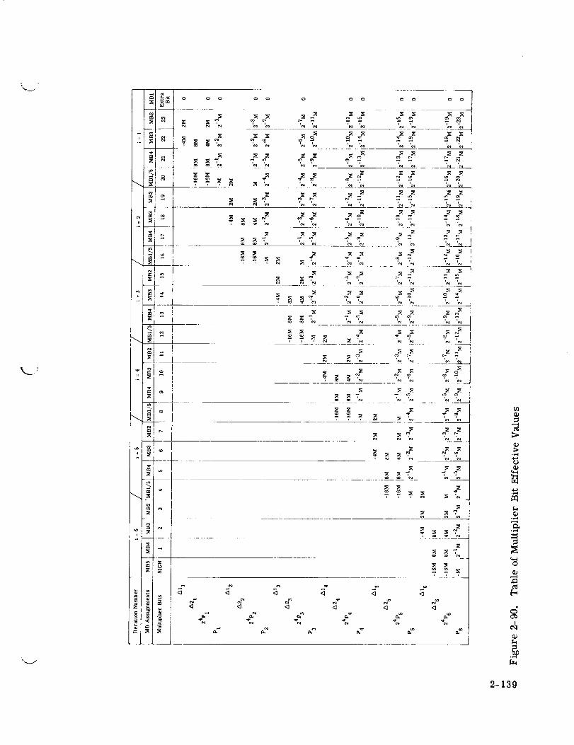
t_1-°
_J_lo-I_ _
i _r
J_F_
e_ t _" I
I_rol
e,i e,l .... e_ '_
_ 'c,l e.l _1
_ZN
1
......... ______ ___
2_
<3
0
I
2-139

2-323. However, bit 20 is evaluated again during iteration two. Values resulting fromthis evaluation will be shifted toward the LSD only twenty places in the final product.The correct value to shift in this iteration is +M. Bit 20 causes A12 to take the value+2M, butA21 has since been reduced from -16M to -M by the first LSD shift of fourplaces. Thus, when these two values are summed, the total effect of bit 20 is +M initeration two, the correct value. These operations are easily followed in figure 2-90.
2-324. As notedpreviously, the values of All andA2i are formed by shifting the mul-tiplicand toward the MSD from one to four places. The shift is relative to the partialproduct which offsets the delta values from the partial products, causing a problem inthe summations required by the multiply formula (20). Counting from the partial productsign, the delta values have fewer bits toward the LSD than the partial products and thepartial products have fewer bits toward the MSD than the delta values, thus
Delta Value = S 1 2 3 4 5 6 23 24Partial Product = S 1 2 19 20 21 22 23 24
4-----MSD _ LSD-----_
The delta values are easily corrected by forcing vacated bits to zeros as the number isshifted. Adding zeros to the LSD end of a number does not change its value.
Delta Value = S 1 2 3 4 5 6 23 24Partial Product = S 1 2 19 20 21 22 23 24
The same solution, however, is not valid for extending the MSD end of the partial products.In order to extend a two's complement number to include more significant digits, theadded bits must be filled with the sign of the number.
Delta Value = S 1 2 3 4 5 6 23 24 0 0 0 0Partial Product = S 1 2 19 20 21 22 23 24
If the partial product is positive, the blank positions are filled with zeros. If the partialproduct is negative, it is in two's complement form and, when extended, must remain inthe correct form for a two's complement number, equation (1). The reason for fillingpositions MSD of the sign with the sign is shown by evaluating a negative number contain-ing all ones before and after extension.
V
V
Before Extension
Form -bsig n× 20 +b 1 x 2-1 +b 2× 2 -2 _- . ° •
Value -1 + 1/2 + 1/4 +...
Mter Extension
Form -bsig n × 24 23 22+ bsig n × + bsig n × + bsig n
+b lx2 -1 +b 2x2 -2 +...
x 21 20+ bsig n ×
2- 140

Value 16 + 8 + 4 + 2 + 1 + 1/2 + 1/4 +...
Both numbers are expressed as "sign plus magnitude" and the sign in both numbers has
the same total value, -1. Thus, both numbers express the same value.
NOTE
k,_J
For delta values which are not shifted the
full four places, the unused places arefilled with the value of sign in the same
manner as the partial products.
2-325. MULTIPLICATION LOGIC CIRCUITS. The multiplication logic circuits are acti-
vated by three instructions; multiply (MPY), multiply and hold (MPH) and divide (DIV).
The use of two multiply instructions provides the option of concurrent operations in the
Add-Subtract Element; the instructions are described in detail in subsequent paragraphs.
2-326. Manyofthe circuits used in multiplication are also used for division. Where
circuit operation is common or the differences minor, the circuit is described here;where the difference is major, the circuit is described here for multiplication and again
for division. The shaded blocks in the illustrations are active only during division andare discussed later.
2-327. The multiply circuit, figure 2-91, consists of three parts; the Command Circuit,Timing Circuits and the Arithmetic Registers. These circuits multiply (and divide) by
an iterative process of two phase-times per cycle. Fifteen phase-times are required to
complete a multiply instruction. The command circuit stores the comnmnded instruc-
tion and provides enabling levels to the timing circuits and arithmetic registers. The
timing circuits define the two phase-time cycle and terminate the process when com-
plete. The arithmetic registers circulate the operands and implement the multiplication
formula described previously.
NOTE
Figure 2-101 is a timing diagram whichshows the detailed timing of the majormultiply circuits. Though the figure is
not referenced directly from the circuitdescriptions, its frequent use is very
helpful in correlating the various parts ofthe multiply logic.
2-328. Command Circuit. The command circuit, figure 2-92, consists of two latches,HOY and VOY which store the three instructions that activate the multiply circuits.
Figure 2-92 gives the states of the HOY and VOY latches for each of the instructions
they store.
2-141

COMMANDCIRCUIT
MULTIPLICAND '
MULTIPLICAND REGISTER
V
24pi
PARTIAL PRODUCT REGISTER
P6
MULTIPLIER
MULTIPLIER AND PRODUCT-QUOTIENT REGISTER
PRODUCT-QUOTIENT
ARITHMETIC
ELEMENT
Figure 2-91. Multiply Circuit, Block Diagram
2-329. The set-input gates for the HOY and VOY latches sense the outputs of the Opera-tion Code Register during bit-times 2 through 8 of every phase B time. Once set, theselatches must not be disturbed until the commanded operation is complete. Thus, their
resetting gates are controlled by the timing circuits which terminate the multiply anddivide processes. The HOY latch is reset at bit-time 2- Z, and the VOY latch at bit-
time 5-Y, of the first phase A following completion of the commanded operation.
2-330. Timing Circuits. The multiply and divide processes are divided into three
phases. During the first phase, the operands are loaded into their respective registersand computations are started; during the second phase, the remaining computations are
completed. The third phase is the period between operations during which the product(or quotient) is circulated for use elsewhere in the computer. The timing circuits con-
sist of two latches which define the two-phase cycle upon which the multiplication anddivision processes are based and a phase counter. The phase counter controls the
phase (or stage) of the processes and terminates them when complete.
MJ
2-142

G2V--
PBV--
OPIV-- A
OP2VN--OP4VN
PAV----t
P2VN--_ A
_TMVN ---]__
z_G2V _
PBV--
OPIV-- A
OP3VN -- _ VOYVOP4VN
G5V--! OYVN
PCVN-- APIVN_
P2VN u
INSTRUCTION
MULTIPLY
MULTIPLY AND HOLD
DIVIDE
ABBR.
MPY
MPH
DIViJ
OP4 OP3 OP2 OPI HOY VOY
0 0 0 1 1 1
0 1 0 1 1 0
0 0 1 1 0 1
NOTE: SEE FIGURE 10-4 (SHEET I)FOR DETAILED LOGIC
Figure 2- 92. Command Circuit
2-331. The TM and DTM latches define the basic two-phase cycle used in multiplicationand division. Figure 2-93 shows how these latches are connected. During a multiplica-
tion instruction, TM is a "I" from the 4-Z time near the start of the cycle until the 14-Ztime at the end of the cycle; during division, TM starts at 7- Z time. DTM is a "l" dur-
ing the last half of the cycle, from 2- Z time until 2- Z time, for both instructions.
2-332. Thephase counter, figure 2-94, is composed of an exclusive zero tratch, chan-nel three of the DL31 delay line and the "stop process" (STP) latch. The output of thetratch bearing the zero determines which phase of the process is underway. The tratch
is set to the phase one and phase two conditions by timing signals under control of thecommand circuit. Phase one starts at bit-time 2-Y of the first phase B of the multiplyinstruction. Phase two starts two phase times later at A-1-Z time.
2-333. The tratch is also set to the phase three, or "process complete" condition bytiming and the command circuit, but with the additional control of the STP latch. Phase
three starts at bit-time 5-Y of phase C; the STP latch determines which phase C.
2-334. During phase one of a multiplication, gate A7 clocks a "1" into channel 3 of theDL31 delay line at B-11-Y time. The "1" emerges from the delay line fifteen and one-half bit-times later at the STP latch.
2-143

G4v 7°TMVNt Ak
HOYV_
f ii::b A hDTMV
DTMVN
Figure 2-93. Multiply-Divide Timing LatchesNOTE: SEEFIGURE 10-4 (SHEET 1)
FOR DETAILED LOGIC
2-335. The ZN signal zero-drives the STP latch set every Z clock-time. The STP latchcorrects the inversion at the input to the delay line by complementing its output. If a"1" emerges at DL31SA at W clock-time, indicating a "0" was clocked into the delayline, the STP latch is reset and then corresponds to the delay line input. (Refer toDelay Lines paragraph. )
2-336. During phase two of the multiply, the "1" inserted in delay line DL31 in phase
one is recirculated through gate A9 every 16 bit-times. Since the period of circulationis two bit-times longer than a phase time, the "1" shifts two bit-times each circulationcycle. The "1" will appear at the STP latch during C-5 time only in the fifth phase Cafter the multiply was initiated. At that time the multiplication process is complete andis terminated by setting the phase counter to phase three, process complete.
2-337. Arithmetic Registers. The multiplication formula is instrumented by manipu-lating the contents of the- circulating shift registers shown in figure 2- 91.
v
2-338. The multiplicand and multiplier registers circulate the operands. The partialproduct register stores the partial products and its associated circuits sense the oper-ands and from them form a new partial product according to the multiply formula eachtwo phase-time cycle. When the final product has been formed, the multiplier registeris extended to form the product-quotient (PQ) register. The PQ register stores theresults of all multiply and divide operations for use elsewhere in the computer.
2-339. The multiplicand register consists of channel one of delay line DL44 and eightlatches, MD0 through MD7, as shown in figure 2-95. This register circulates its con-tents once every two phase-times, and thus does not shift. During the first phase of amultiplication, the contents of the addressed memory location enter the MD1 latch fromthe TRS line. The entire 26-bit data word is transferred, but the two low-order bitsare ignored throughout the multiplication process.
2-144 Changed 4 January 1965 _.J

Z
>
Z>
Z> 0 _ _
iii
ZN
Z
..J
> o-U 0
I
I>o-
l
I
_o
--7) !
Ill
V
'.iI_°°__u
IO
Z--'
_o
"'-0_'''_i
I......-
0Z
O
H
!
_2
2-145

(2 PHASE-TIMES)
Figure 2-95. Multiplicand Register, Block Diagram
2-340. The multiplicand is entered through gates A4 and A1, figure 2-98, beginning atB-4-X time. The MD1 latch is reset by the W clock at bit-time B-4 and all followingbit-times until the entire data word is entered. The latch is set a X clock-times, ifTRS is a "1. " At Y clock-times, the contents of the MD1 latch are transferred into theMD2 latch. The previous contents of the register enter the MD1 latch from the MD0latch at Z clock-times. This data is destroyed in the MD1 latch when it is reset at the
following W clock-time.
2-341. Whenthe sign of the multiplicand has entered the MD1 latch, the entry gates aredisabled and the register loop is closed. Gate A1 is disabled at bit-time 1-Y whenTBCV goes to a "0" and gate A4 is disabled by P2VN at bit-time 1-Z. The low-orderbit of the multiplicand returns to the MD1 latch at bit-time 3-Z. Thus, the previouscontents of the register which entered MD1 at bit-times 1-Z and 2-Z are allowed tocontinue circulating. The values of these bits cannot be determined.
2-342. The multiplicand register is also used as temporary storage for the automaticHOP-constant save circuit. The HOP constant enters the multiplicand register fromthe NU latch via gate Ag. Details of the HOP-constant save circuit are given in the de-scription of the Program Control Element.
2-343. The multplier register, figure 2-96, consists of channel two of delay line DL44and latches MR0, MR1, MR2 and Q1. Note that this register contains fewer latchesthan the multiplicand register; therefore it shifts its contents four places toward theleast significant digit (LSD) each two phase-time cycle. This shift brings four newmultiplier bits into sampling position each iteration. The Q1 latch is not included in theloop of the register, but provides a delayed output of the MR2 latch to the circuits whichsample the multiplier bits.
2-344. While the multiplicand is entering its register, the contents of the accumulatorregister are transferred into the multiplier register through the MR1 latch. This is adouble line transfer from the AI2 latch through gates A6 and A9, figure 2-99, beginningat B-5-Y time. Only the 24 high-order bits are transferred, but during bit-times 3 and4, "O's" are entered in the two low-order positions. At bit-time 3-X, the MR1 latch isreset by gate A10; it cannot be set again until bit-time 5 when TMV becomes a "1".
2-345. The "0" inserted at bit-time 3 has no significance, but the "0" from bit-time 4
is imperative for a valid multiplication. This "0" is the extra bit added to the multipliershown in the last term of equation (6) of the multiply formula derivation; it is discussed
in paragraph 2-310. X_]
2-146

2-346. Tile Partial Product Register, figure 2-97, consists of ehannel four of delay line
DL44 and latches PR, PRO. PR1 and PR2. Like the multil)lier register, its capacityis 24 bits which are LSD-shffted four places each two phase-time cycle. The shift di-vides 24p iby sixteen lu form Pi-1 for the next iteration. The output of the PR0 latch isPi-1.
MULTIPLIER (2 PHASE-TIMES LESS 4 BIT'TIMES)
(MULT,PL,ERINSERT,O
AI2(PROCESSl _ [_'_I"_----_
PRODUCT-QUOTIENT
(3 PHASE-TIMES)
AL PRODUCT INSERTION)
TAOITHMETIC
ELEMENT
Figure 2-96. MultiPlier and Product - Quotient Registers, Block Diagram
(2PHASE TIMES LESS 4 BIT-TIMES)
I ['----I F--'---I (Pi-1) (Pi-1 +l_2)
DL 44 _ - PR1
MO5 (8M) MD3 (2M) J
(24pF)
Figure 2-97. Partial Product Register, Block Diagram
2-147


zzoo_
Y
zzz
!
,,,,i


E
o
x • _ z
z
c_
c_
c_
lI'
i


2-347. Duringeach iteration, the product of the 24-bit multiplicand and four new bits oftile multiplier is formed at the output of the PR2 latch. The length of a binary product isthe sum of the number of bits in the operands; thus, a 28-bit product must enter channelfour of DL44 each cycle. Since the length of the product is equal to the length of thecycle, there are no gaps in the register, The sign bit of one product is followed im-mediately by the low-order bit of the next product.
2-348. Eecause the capacity of the partial product register is only twenty four bits. thefour low-order bits of each product are truncated as they enter the PRO latch. Thedouble line transfer gates, All and A12, figure 2-100, are disabled by TMV for four bittimes just after the sign bit is transferred into PRO. With the transfer gates disabled,bits 27 through 24 are ignored. The sign bit was the last bit transferred into the PROlatch and since it is not reset, PRO produces the value of sign for four extra bit times.These four bits account for the offset between the partial products and the delta valuesdiscussed previously.
2-349. Since the value of Pi-1 must be zero for the first iteration of each multil)lication,the partial product register is loaded with all zeros at the completion of each multiply
commaud. When the phase counter switches to phase three, gates A63 and A64, figure2-100, are disabled, forcing zeros into channel four of the DL44 delay line. The firstzero emerges from the PR0 latch at the next A-14-Z time, well before the computationof 24Pl could begin if the next instruction were another multiply command. Gates A63and A64 ,'emain disabled until another multiply or a divide command can restart thephase counter.
2-350. Circuits associated with the partial product register sense the MBbits in themultiplier register to determine the values of A1 iandA2 i. The delta values are thengated through selector latches into adder-subtracter circuits which combine them withPi-1 as it circulates in the partial product register.
2-351, TheAIitratch, figure 2-100, senses bitsMB1 through MB3and stores theabsolute value of Alp
.,
NOTE
The value of A1 i is stored in inverse formas a "0" on a "not-value" line. For ex-
ample: if the MB bits specify the value2M for All, the TMDN (Two times theMultiplicanD Not) output--of the A1 i tratchis switched to a "0" and the other twolines to "l's. "
At the beginning of every multiply cycle, gate A24 resets theA1 i tratch to ZDLN = 0in preparation for sensing the MB bits. At the following bit-time 6, gates A25 and A26sense bits MB1 from the SG2 latch and MB2 from the MR2 latch (nmltiplier register).Lf MB1 and MB2 are different, the A1 i tratch is set to TMDN = 0, indicating that thevalue oral i is either plus or minus 2M. See figure 2-89.
2-150


_.o
e_
!
P'I
III III _AIIIII
Z N
0 z
m,. r
-_mm ]
_._ _ _._Z_, _ +
_"7 _,.
o- .-


i
_-o•
- ,,.-:---
x
Z
0
_0
_Z _
oZ
-1
-_, " ,"-I-"I-,
z >z15
N I I I I
_o _
1
jjl.z zl
0
x I I I I I I
>_z> ,_z
::i:':':':'?':"'i:':':':i:":"
z_ z_ i _z__>o_o_ _o_
I
I x I I I I I I I
" I I I _ I I I I I I I I I I I I I I
> zz,_sz > z"r


..-:o =_-z_
,[.i........
,_"o I o -,o8_
II IIII
_. 7_ _,z_

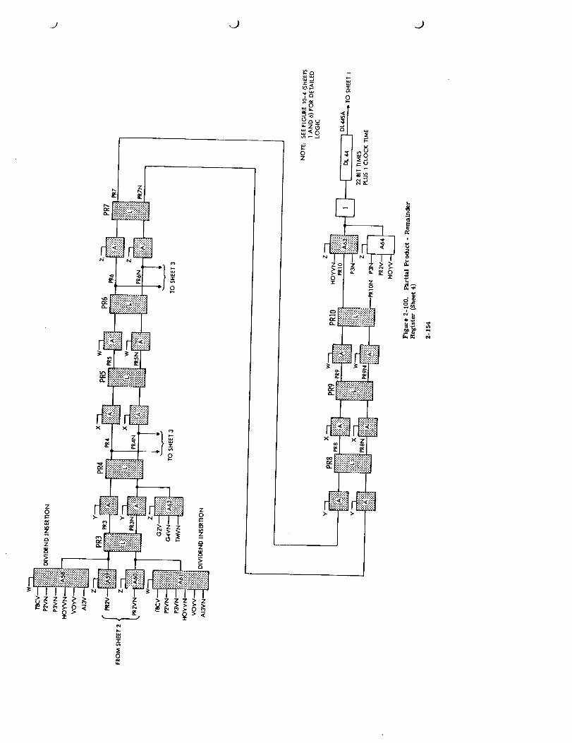
J ..J .j
g£
_"2,'-,u
(3Z
Zo
--- z
iI
!


N
N4
I
NI
EiS
4


2-352. Atbit-time 7, gatesA29andA30senseallthree MB-bits to determine if 4Mis
the A1 i value specified. Bit MB1 is again sensed from the SG2 latch, but bit MB2 hassince been shifted into the Q1 latch and the MR2 latch now contains bit MB3. If 4M isthe value specified, the A1 i tratch is set to FMDN = 0. Gate A27 is used in forcing thevalue of sign into vacant positions of the partial product; this operation is described indetail later. Gate A22 holds theA1 i tratch at ZDLN = 0 forcing the value of Ali to zero
when no multiply or divide instruction is being operated.
2-353. TheA2itratchsenses bits MB3 through MB5 and stores the absolute value ofA2i; its operation is similar to that for rheA1 i tratch except for timing and the pointswhere the MB bits are sampled. Gate A2 resets the tratch to ZDHN = 0 at bit-time 4-Zin preparation for sensing the MB bits. During bit-time 8, gates A4 and A5 sense bitsMB3 and MB4 at latches SG1 and MR2 for the value 8M. At bit-time 9, gates A7 and A8
sense bits MB3 (SG1), MB4 (Q1) and MB5 (MR2) for the value 16M. Gate A6 is thecounterpart of gate A27 for the A1 i tratch.
2-354. Thesignlatches, SG1 and SG2, store the values of multiplier bits MB3 and MB5,
respectively. Operation of the two latches is identical except for timing. Both latchesare reset near the beginning of each multiply cycle and set to the new value one bit-timelater. Since bits MB3 and MB5 determine the signs of the delta values (figure 2-89)the SG1 and SG2 latches provide sign control for the adder-subtractor circuits.
2-355. Thetimingofthe SG2 latch has special significance. Multiplier bit MB5 of oneiteration is also bit MB1 of the following iteration. The SG2 latch, which stores MB5,is not reset until bit-time 7-Z, two clock-times after its contents are sampled as MB1
at the A1 i tratch. Thus, the SG2 latch stores bit MB5 during one iteration and (effec-
tively) MB1 during the first part of the next.
2- 356. The TFD and ESD latches, figure 2-100, are the selector latches through whichthe delta values are gated. The TFD latch produces the A1 i value which can be eitherTwo or Four times the multiplicanD. The ESD latch produces the A2 i value of either
Eight or-Sixteen times the multiplic--anD. The delta tratches determine which of the twov--alues each latch will produce.
2-357. As noted previously, A 1 i andA2 i are formed by shifting the multiplicand relativeto the partial product. The shift is accomplished by allowing the multiplicand to cir-culate farther through its register (before it is sampled) than the partial product. Thecontents of the multiplicand register are sampled at four latches along its length andthe outputs applied to the TFD and ESD latches. The outputs of the sampled latches(MD2, MD3, MD4 and MD5) are the multiplicand shifted 0, 1, 2 and 3 places, and cor-respond to the values M, 2M, 4M and 8M, respectively. The TFD and ESD latches shiftthe values one more place to for,n the correct delta values.
2-358. The outputs from latches MD2 and MD3 are applied to the TFD latch; outputsfrom the MD4 and MD5 latches are fed to the ESD latch inputs. The A1 i andA2 i tratches
select which input is gated through each latch according to the delta values. For ex-ample: the MD5 (8M) inputs cause the ESD latch to produce 16M at its output. Thus,the MD5 inputs are enabled by A2 i tratch outputs ZDHN and EMDN both being "l's"which indicates that the SMDN (16M not) output is a "0" (delta values are stored in in-verse form).
\
(
2-156
(


2-359. Gate A18, figure2-100, resetsthe ESD latch at bit-times 5 through 7 before theA2 i value is stored in its tratch. The ESD latch cannot then be set until bit-time 8, justbefore the first bit of the multiplier can appear at its inputs. Gate A35 resets the TFDlatch at bit-time 5, which results in the same timing considerations for the A1 i circuits.Gate A37 resets the TFD latch when the multiply process is complete; gate A19 resetsthe ESD latch after completion.
2-360. The outputs of the TFD and ESD latches are fed to the adder-subtractor circuitswhich combine the delta values with the previous partial product. The K1 and PR1latches form one adder-subtractor which computes
Pi-1 +A2i
The K2 and PR2 latches form another adder-subtractor which computes
(Pi-1 +A2i) + Ali
The output of the PR2 latch is 24Pi .
2-361. The PR1 and PR2 latches are basic serial binary adders; their four input gates(figure 2-100)correspondtothe add-subtract logic in the Arithmetic Element. The K1and K2 latches store the carry or borrow from one bit to the next; the signs of the deltavalues determine which conditions K1 and K2 will store for each computation cycle. TheSG2 and SG1 latches store these signs and control K1 and K2 respectively.
2-362. The PR1 latch is reset at every Z clock-time by the ZN zero-drive signal. Atthe following W clock-time, PR1 is set if the sum (or difference) bit is a "1". At Xclock-time (after the sum has been stored) the K1 latch is set to the carry or borrowcondition for the next bit. The K1 latch is reset during bit-times 5 through 8 (gate A21)at the beginning of every cycle to assure that no carry or borrow is propagated from oneiteration to the next. Bit-times 5 through 8 coincide with the reset time for the ESDlatch. Thus, the K1 latch does not sense carry or borrow when one of the operands isnot available.
2-363. Operation of the PR1 and PR2 latches is identical except for timing and bothlatches add continuously. When no addition is required, the K1 and K2 latches are resetand the delta values are forced to zero. The K1 and K2 latches also operate alike ex-cept for reset timing. The K2 latch reset timing coincides with that for the TFD latch.For a discussion of the gates which determine the sum and the carry or borrow, referto the Arithmetic Element.
2-364. Whenthe multiply process is complete, the Product-Quotient (PQ) Register,figure 2-96, is formed by extending the multiplier register to include channel two ofdelay line DL31 and latches QS, QSD, Q9 and PQR. This register stores the final pro-duct and circulates it every three phase times for use elsewhere in the computer. Onceloaded, its contents can be changed only a store (STO) instruction addressing the PQregister, by a divide instruction (DIV) or by another multiply instruction. The PQ reg-ister is assigned memory address 775 and can be addressed with all the arithmeticinstructions except MPY, MPH and DIV.
2-365. Allpartialproducts enter the Q8 latch through gates A18 and A21, figure 2-99,from the PR latch in the partial product register. However, due to the timing of TBCVat gate A15 only partial products P3 and P6 ever reach the PQR latch intact. No datacan circulate beyond the PQR latch until phase three of the multiply process.
2-157

NOTE
Partial product P3 canbe usedby address-ing the PQregister with the secondin-struction following anMPY. The resultis theproduct of the multiplicand and thetwelve LSD bits of the multiplier. Sam-piing P3 does not affect the operation ofthe multiply circuit and the final productwill be computed as usual.
2-366. The phase counter switches to the phase three condition just as product P6, thefinal product, begins entering the PQR latch. Gates A2, A17 and A22 are enabled atthis time and the loop of the PQ register is closed. Simultaneously, gate A1 opens theloop of the multiplier register. Gates A18 and A21 continue entering product P6 intothe PQ register until the command circuit is reset, signaling the end of the multiplyoperation.
2-367. TheQ8Dlatchprovides a delayed output from the PQ register for use in theArithmetic Element. The input gates to the B latch (in the Arithmetic Element) syn-chronize the QSD output with the other data sources in the computer. Correspondingbits of data from Q8D, TRS and IOREG are available to the B latch during the same bittime.
2-368. As noted earlier, data can be loaded into the PQ register by addressing memorylocation 775 with an STO instruction. This operation transfers the accumulator contentsinto the Q9 latch. The transfer is affected by gates A23 and A24, figure 2-99. Theaccumulator contents enter the Q9 latch through gate A24 on the AI3 line. Gate A23blocks the previous contents of the register by holding the Q8 latch reset until thetransfer is complete. Both gates bear the operation codes for STO and DIV and theTTLV signal. The TTLV signal is a "1" when memory location 775 is selected.
2-369. Computation Cycle. The math flow of a multiply computation cycle is shown infigure 2---I02. TheAliandA2 i tratches are initialized to show delta values of zero inpreparation for sensing the MB bits. The SG1 latch is reset before sensing the sign of/kl i and the TFD latch is reset to assure a starting condition of "0".
2-370. TheAlitratchthen senses bits MB1 and MB2 to determine if the magnitude of
A1 i is 2M. If 2M is the specified value, the A1 i tratch is set to gate the MD2 outputthrough the TFD latch. The SG1 latch then senses MR1 for the sign of A1 i. If MR1 isa "1", the sign of A1 i is negative and the SG1 latch is set. The SG1 latch then conditionsthe K2 latch to borrow for the duration of the cycle. If MR1 is a "0", the SG1 latchremains reset, indicating a positive delta value, and the K2 latch is conditioned tocarry.
2-371. IfthevalueofA1 i had not been 2M, the sign ofA1 i would have been sensed im-
mediately. TheA1 i trafch then senses bits MB1, MB2 and MB3 to determine if the valueoral i is 4M. At this point in the flow, the value ofA1 i must be either 4M or 0. IfMB1, MB2 and MB3 are all alike, the value is zero and theAli tratch remains reset.The TFD latch also remains reset, producing a delta value of zero, and the multiplycircuit begins sensing the sign and magnitude of A2 i. If the MB3 bit is not the same asMB1 and MB2, the value oral i is 4M and theA1 i tratch is set to gate the MD3 outputthrough the TFD latch.
V
k#
2-158

IIU U
U
Z -
(_
ioI--.Z
I:Z,_.1 x
8


2-372. The ESD and SG2 latches are then reset to complete initialization of the A2 i cir-cuits. Note that the SG2 latch is not reset until after the A1 i magnitude control has beenset up. The MB1 bit used to determine the value of A1 i is actually the MB5 bit storedin SG2 during the previous iteration. This is the overlap between iterations which allowsthe multiply process to ignore the signs of the operands.
2-373. TheA2itratchthen senses whether multiplier bits MB3 and MB4 are alike. Ifthe bits are alike, the magnitude of A2 i is either 16M or 0. Bit MB5 is then sensed atthe MR1 latch and stored in SG2. Bit MB5 is the sign of A2 i and the SG2 latch conditionsthe K1 latch to carry or borrow depending on whether the sign is plus or minus.
2-374. Bits MB3 and MB4 are then sensed with bit MB5 to determine whether the mag-nitude of A2 i is 0 or 16M. If MB5 is different than MB3 and MB4, the magnitude ofA2 i is 16M and theA2 i tratch is set to gate the MD5 output through the ESD latch. Ifbits MB3 and MB4 had been different when sensed alone, the magnitude of A2 i would be8M. When 8M is the value specified, theA2 i tratch is set to gate MD4 through the ESDlatch before the SG2 latch determines the sign.
2-375. Itwas noted earlier thatA2 i is summed with the previous partial product beforeA1 i. An apparent paradox arises when this fact is considered with the fact that the
value of A1 i is sensed first and begins emerging from TFD beforeA2 i is availablefrom ESD. The solution to the paradox lies in the distances by which the delta valuesare offset from partial products.
2-376. TheAlivalue is offset by either 1 or 2 places; the/k2 i value is offset by either3 or 4 places. Translated into machine operation, the offset places become delays ofcorresponding numbers of bit times. Thus, though the partial product passes throughtheA2 i summing circuit first, meaningful data is available for A1 i before it is availablefor A2 i. Bit-for-bit, A2 i is summed with the partial product first though/kl i dataenters the summation earlier.
2-377. Once the magnitude and sign control has been set up, the adder-subtractor cir-cuits (KI° PR1 and K2-PR2) compute the sums indicated by the multiply formula auto-matically until near the end of the cycle. At the second bit-time 2-W, the magnitude
oral i is sensed for non-zero. If the value is not zero, theA1 i tratch is forced to 4M.
2°378. Ifthe specifiedvalue oral i was 2M, the tratch is forced just after the sign ofthe multiplicand is transferred from MD2 to TFD. Forcing the tratch switches the TFDinputs from MD2 to MD3 and at the next bit time, the sign is transferred to TFD again.At bit 3-Y time, the A1 i tratch is reset, deconditioning all the data gates to the TFDlatch. Since the TFD latch contains the sign and is not reset until the end of bit time 5,it stores the value of sign for an additional two bit times. Thus, the unused bit positions
more significant than sign are filled with the value of sign. At bit-time 3- Z, the A2 itratch is sensed for non-zero to force sign into any unused bit positions of A2 i.
2-379. DIVISION. The Multiply-Divide Element implements a modified form of non-restoring division in which two quotient bits are formed each two phase-time cycle. Theresulting 24-bit quotient is available to the eighth and subsequent instructions followingDIV by addressing the PQ register with an arithmetic instruction. Division is limited toproblems in which the divisor is larger than the dividend so that the quotient will not
(
2-160 Changed 4 January 1965


k._j
exceedthe capacityof its storage register. The description of the division processbegins with an introduction to both the restoring and the nonrestoring division techniques.A thorough understanding of basic nonrestoring division is an essential precept of thedivision process implemented in the computer.
2-380. _Restoring Division. Figure 2-103 illustrates a binary division problem and Rssolution by the restoring divide technique. The first operation is to subtract the divisor(D) from the dividend (denoted as remainder RI). This subtraction is unsuccessful sinceit changes the sign of the remainder (R 1 is positive, R2 is negative). Since the divisorcannot be subtracted from the remainder, the remainder is not divisible by the divisor;thus, the first quotient bit (QI) is a "0". Because the correct remainder was destroyedby the subtraction, it must be restored (hence the name of the process) by adding backthe divisor to form R 3 (R 3 = Rl). Remainder R3 is then shifted one place toward theMSD and another subtraction is performed. This subtraction is successful as evidencedby the positive remainder; thus the second quotient bit (Q2) is a "I".
2-381. Note that WHEN THE SIGN OF THE DIVISOR AND THE SIGN OF THE RE-MAINDER ARE ALIKE, THE QUOTIENT BIT IS A 'T'. This relation is true regardless
of the signs of the dividend and divisor.
2-382. Remainder R 4 need not be restored since the subtraction which formed it wassuccessful. Thus, it is merely shifted one place toward the MSD preparatory to thenext subtraction. The divisor is then subtracted from 2R4, but the subtraction is un-successful since the sign of the result is unlike the sign of the divisor. Thus, the third
quotient bit (Q3) is a "0".
2-383. Before another subtraction can be performed, the previous remainder must berestored by adding the divisor to the present remainder, forming R6. Remainder R6 isthen shifted one place toward the MSD and the divisor is subtracted from the result.The remainder formed by this subtraction (R7) is zero and since its sign and the sign ofthe divisor are alike, a "1" is placed in the fourth quotient bit.
2-384. The divide process can be continued to obtain as many quotient bits as are de-sired. In the sample problem, any additional quotient bits will all be "O's" because theremainder, having gone to zero, will remain unchanged. Subtraction from zero givesa negative remainder (and a "0" quotient bit) which must be restored, resulting in an-other zero remainder for the next subtraction, etc.
2-385. Nonrestoring Division. Nonrestoring division eliminates the need for an extraoperation to restore the remainder when an unsuccessful subtraction occurs. This fea-ture shortens the division process considerably, as shown by figure 2-104. Restoringand nonrestoring division are identical until an unsuccessful subtraction occurs, suchas the first subtraction in the sample problem. Restoring division performs the follow-ing steps after an unsuccessful subtraction to obtain the next remainder sensed to deter-mine a quotient bit:
1) Add the divisor R 2 + D = R 3
2) Shift the result MSD 2(R 2 + D) = 2R 3
3) Subtract the divisor 2(R 2+D)- D=R 4
\ Y
Changed 4 January 1965 2-161

Problem:
Solution:
25×2 -6 + 5x2 -3 =Q
Divisor (D)= 0 . I 0 1 (5x2 -3)
Dividend(Rl) = 0 0 1 1 0 0 1
Q1
0
D 0. 101/0
0
R 2 I
0
R 3 0
2R 3 0
0
R 4 0
2R 4 0
0
R 5 i
0
R 6 0
2R 6 0
0
R 7 0
Q2 Q3 Q4
• 1 0 1
0 1 1 00
• 1 0 1
• 1 1 0 0 0
1 0 1
0 1 1 001
1 1 0 010
1 0 1
0 0 1 0 1 0
0 1 0 100
1 0 1
1 0 1 100
1 0 1
0 1 0 100
1 0 1 0 0 0
1 0 1
0 0 0 0 0 0
(25 × 2-6)
Figure 2-103. Sample Restoring Divide Problem
Quotient (Q) = 5 x 2-3
R 1
Subtract D
Negative remainder, Q1 = 0
Add D to restore R 1
R 3 = R 1
Shift R 3 MSD
Subtract D
Positive remainder, Q2 = 1
Shift R 4 MSD
Subtract D
Negative remainder, Q3 = 0
Add D to restore 2R 4
R 6 = 2R 4
Shift R 6 MSD
Subtract D
Positive remainder, Q4 = l
%2
2-162 Changed 4 January 1965
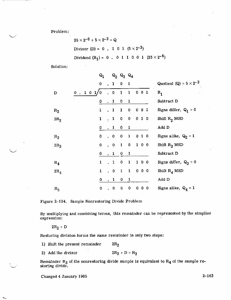
Problem:
Solution:
D 0
R2
2R2
R3
2R3
R4
2R4
R5
25x2 -6+ 5x2 -3 =Q
Divisor (D)= 0 . 1 0 1 (5x2 -3)
Dividend(R I) = 0 . 0 1 1 0 0 1
. 1
Q1 Q2 Q3 Q4
0 . 1 0 1
01/0 . 0 1 1 001
0 . 1 0 1
1 . 1 1 0 001
1 1 0 0 010
0 1 0 1
0 0 0 1 010
0 . 0 1 0 100
0 . 1 0 1
i 1 0 1 100
1 0 1 1 000
0 . 1 0 1
0 . 0 0 0 000
(25 x 2-6)
Quotient (Q) = 5 x 2-3
R I
Subtract D
Signs differ,Q1 = 0
ShiftR 2 MSD
Add D
Signs alike,Q2 = 1
ShiftR 3 MSD
Subtract D
Signs differ,Q3 = 0
ShiftR 4 MSD
Add D
Signs alike,Q4 = 1
Figure 2-104. Sample Nonrestoring Divide Problem
- /
By multiplying and combining terms, this remainder can be represented by the simplierexpression:
2R 2 + D
Restoring division forms the same remainder in only two steps:
1) Shift the present remainder 2R 2
2) Add the divisor 2R 2 + D = R 3
Remainder R 3 of the nonrestoring divide sample is equivalent to R 4 of the sample re-storing divide.
Changed 4 January 1965 2-163
2-386. Thusthe procedurefor nonrestoring division canbe statedas follows:
1) Subtract the divisor (D) from the dividend(R1).
2) Comparethe divisor sign with the remainder sign and makethe quotientbit a "1"for like signs, or a "0" if the signs are different.
3) Shift the remainder oneplacetoward the MSD.
4) If the previous quotientbit wasa "1", subtract the divisor from the shifted remainderor, if the quotientbit wasa "0", addthe divisor.
5) Repeatstep 2 to determine the next quotientbit andsteps3 and4 to form a newre-mainderuntil the desired numberof quotientbits is obtained.
2-387. Nonrestoring division canbe further condensedby shortcutting the determinationof the quotient sign. Sincethe sign of the quotient is dependentonly on the signs of thedivisor anddividend, it canbedeterminedby inspectionandno shift or subtraction isprerequisite. It is a curious fact that the rules for determiningthe sign of the quotientare the inverse of the rules for determiningthe valueof a magnitudebit. If the signs ofthe divisor anddividendare alike, a "0" shouldbeplaced in the quotientsign to indicatea positive result. If the divisor sign matchesthat of a remainder later in the process,a "1" is placedin the quotient. However, a divide circuit canuse the latter relation-ship to form all quotientbits, including sign, andthencomplementthe sign at a latertime to correct it. Correcting the sign creates nospecial problems in division becausethe sign is the first bit formed andis not altered by subsequentcomputationsas is thecasein multiplication. The problempresentedin previous samplesis solvedagaininfigure 2-105usingthe sign shortcut.
2-388. Note that the first subtractiongivenin the rules for nonrestoring division iseliminatedby the sign shortcut. Division thenbecomesessentially a two-step process:
1) Comparethe divisor andpresent remainder signsto determine the quotientbit.
2) Form the next remainder by shifting the present remainder andeither addingorsubtractingthe divisor.
This is the division techniqueuponwhichthe computer's division process is based.
2-389. Computer Division. In computer division two quotient bits are formed eachiteration. The first quotient bit is determined from the divisor and present remaindersigns, as in the shortcutted nonrestoring process. The second quotient bit is formedby predicting the sign of the next remainder in advance and comparing it, by a uniquemethod, with the divisor sign. The divide circuit then forms the next two remaindersalmost simultaneously. Although a quotient bit has already been based on the predictedvalue of the "next remainder" sign, that remainder is generated as an intermediate stepin the development of the "second remainder". The second remainder then becomes the"present remainder" for the following iteration during which two more quotient bits areformed.
2-164 Changed 4 January 1965

Problem:
Solution:
SignCorrection:
D
2R 1
R 2
2R 2
R 3
2R 3
R 4
25x2 -6+ 5x2 -3 =Q
Divisor (D) = 0 . 1 0
Dividend (RI) = 0 . 0
i (5 x 2-3)
1 1 0 0 I
0 . 1
Q1
• o010
0
0
0
0
0
1
1
0
0
_r
Q2 Q3 Q4
1 0 1
0 1 1
1 1 0
1 0 1
001
010
0 0 1 010
0 1 0 100
1 0 1
1 0 1 1 0 0
0 1 1 0 0 0
1 0 1
0 0 0 0 0 0
(25 x 2-6)
R1, signs alike, QI = 1
Shift R 1 MSD
Subtract D
Signs alike, Q2 = 1
Shift R 2 MSD
Subtract D
Signs differ, Q3 = 0
Shift R 3 MSD
Add D
Signs alike, Q4 = 1
Complement sign
J
Figure 2-105. Nonrestoring Divide with Sign Shortcut
2-390. As previously noted, the "next remainder" is formed by shifting the presentremainder one place toward the MSD and then either adding or subtracting the divisor.The sign of the next remainder is determined by the summation of the signs of the divisorand the shifted present remainder with the carry (or borrow if subtracting) into the signposition. The value of the sign bit can then be accurately predicted if the following in-formation is available:
I) Sign of divisor
2) Sign of shifted present remainder
3) Value of carry into sign position, if adding
4) Value of borrow into sign position, if subtracting
5) Whether divisor will be added or subtracted.
Changed 4 January 1965 2-165

Thetruth table for summationof the two signs with the carry or borrow is showninfigure 2-106, expandedto includethe secondquotientbit. The summationis the samefor boththe carry andborrow, thus onetruth table showsthe sign bit developedby eitheraddition or subtraction of the divisor.
Signof Shifted Signof Next SecondQuotientRemainder Signof Divisor Carry or Borrow Remainder Bit
0
0
0
0
1
1
1
1
0
0
1
1
0
0
1
1
0
1
0
1
0
1
0
1
0
1
1
0
1
0
0
1
1
0
1
0
0
1
0
1
Figure 2-106. Truth Table for SecondQuotientBit
2-391. As shownin the truth table, the secondquotientbit is a "1" wheneverthe signof the divisor matchesthe predicted sign of the next remainder. This agreeswith therules for nonrestoringdivision presentedearlier. Closer examinationof the truth tablereveals that in eachcasewherethe quotientbit is a "1", the sign of the shifted remain-der andthe carry or borrow conditionalso match. Thusthe secondquotientbit canbedeterminedfrom these factors andpredicting the sign of the next remainder neednot bedone. This is the "uniquemethod"by which the divisor sign is comparedwith the "pre-dicted next remainder sign". Althoughthe prediction is not actually made, it is in-herent in the information usedto form the secondquotientbit.
2-392. In terms of basic machineoperation, the computer divides in the following man-ner (seefigure 2-107). As the divisor andfirst remainder (dividend)enter their re-spective registers, they are monitoredby two latches (Carry- Borrow). Onelatch keepstrack of the carry function as thoughthe divisor were beingaddedto the shifted re-mainder. The other latch keepstrack of the borrow as thoughthe divisor were beingsubtractedfrom the shifted remainder. Sincethe remainder hasnot yet beenshifted,the 2-1 bit is monitoredby the carry andborrow latches to simulate the shift. As soonasthe signs of the divisor andremainder are loaded, the first quotientbit is formed,basedona comparisonof the two signs, andplacedin temporary storage (Qi). Thefirstquotientbit, in accordancewith the rules for nonrestoringdivision, determineswhetherthe divisor will be addedor subtractedto form the next remainder. This, in turndecideswhether the carry or the borrow conditionwill beusedto determine the secondquotientbit. Thusthe carry (or borrow) into the sign position is comparedwith the signof the shifted remainder to determinethe secondquotientbit which is placedin Qi+l.Becausethe remainder still hasnot beenshifted, the shifted remainder sign is sensedfrom the 2-1 bit whichwill, after the shift, becomethe sign. As soonas thetwo quotientbits havebeenformed, theyare loadedinto the QuotientRegister. During the first
2-166 Changed4 January1965

COMMAN D
Cl RCUl T
TIMI NG
CIRCUIT
,,---lid
PR &PRO
DIVISOR REGISTER
REMA! NDER REGISTER
DI
PR2 - PR10
CARRY-
BORROW
F
,J QUOTIENT REGISTER
I,q PRODUCT-QUOTIENT REGISTER
i
ARI THM ETI C
ELEMENT
v Figure 2-107. Divide Circuit, Block Dia4_ram
Changed 4 January 1965 2-167
iteration, the first quotient bit is complemented in the quotient register to correct thesign. Recall from the description of nonrestoring division that the sign bit must beformed incorrectly in order to select the correct operation (add or subtract) to computethe next remainder. Thus the original quotient bits are retained in temporary storageto control formation of the remainders.
2-393. As the present remainder circulates in its register, it is shifted two placestoward the MSD, one place for each of the two remainders which must be formed. Theshifted remainder then enters two adder-subtractor circuits in serial. The outputs ofthese adder-subtractors are the two remainders formed each iteration.
2-394. The first adder-subtractor forms twice the "next remainder" by adding or sub-tracting (depending on the value of the first quotient bit) twice the divisor from fourtimes (MSD shift of two) the "present remainder". Thus the output of the first adder-subtractor circuit is shown by the expression
4R i + 2D (1)
where i is the number of the "present remainder".
This expression can be simplified to
2(2R i + D) (2)
Since the "next remainder" (Ri+l) is formed by shifting the "present remainder" oneplace toward the MSD (2Ri) and adding or subtracting the divisor (+D), twice the "nextremainder" is shown by equation (2), which represents the output of the first adder-subtractor. Thus, the output of the first adder-subtractor is the "next remainder" pre-shifted in preparation for forming the "second remainder". The output of the secondadder-subtractor is the "second remainder" or the "present remainder" for the nextiteration. As the last bits of the new remainder are formed, the first bits approach thecarry and borrow latches. This begins the cycle for forming the next two quotient bits.
2-395. DIVISION LOGIC CIRCUITS. The division logic circuits perform the iterativedivide process previously described when activated by the DIV instruction. The DIVinstruction requires 27 phase times for completion during which the following operationsare performed:
1) The Divide (DIV) instruction is read from memory and decoded.
2) Two quotient bits are developed during each iteration until the final 26-bit quotientis determined. This quotient contains 24 significant bits, the two low-order bits arezeros.
3) The final quotient is stored in the Product-Quotient (PQ) register.
2-396. The division process begins when the DIV instruction is decoded. The operandaddress of the DIV instruction specifies the memory location of the data word to be usedas the divisor; the contents of the Accumulator Register are used as the dividend.
2-397. The divide circuit (figure 2-107) is composed of essentially the same three parts,Command Circuit, Timing Circuits and Arithmetic Registers, which make up the mul-tiply circuit. Indeed, these parts perform the same general functions for division thatthey did for multiplication. The command circuit stores the DIV instruction until thedivision is complete. Outputs of the command circuit condition the timing circuits to
V
2-168 Changed 4 January 1965

r
slightly alter the two-phase cycle and prolong the phase count to provide the extra timerequired for division. These outputs are also applied to the arithmetic registers, wherethey 1) condition circuits which were not used in multiplication; 2) decondition otherswhich are not used for division; and 3) alter the purpose of others which are common toboth, so that division is affected instead of multiplication. The arithmetic registerscirculate the operands, and the circuits associated with the registers implement the
division process.
2-398. Many of the division circuits are common to multiplication. For detailed de-scriptions of these circuits references are provided to the appropriate paragraphs of theMultiplication Logic Circuits description. These references will assist the reader incorrelating the roles played by common circuits in the two operations. However, if thereader is thoroughly familiar with circuit operation for multiplication, these referencesmay be overlooked to preserve continuity in the description of division.
2-399. Command Circuit. Operation of the command circuit is identical during multi-plication and division except for the instruction codes involved. When a DIV instructionis decoded, the VOY latch is set; the HOY latch remainds reset. See paragraph 2-328and figure 2-92 for details on the command circuit.
2-400. Timing Circuits. (See figure 2-93. ) As in multiplication, the TM and DTMlatches define the two phase-time cycle upon which the division process is based. Fordivision TMV is a "1" from the 7-Z time at the end of the cycle. The DTMV output isa "1" during the last half of the cycle, from 2-Z to 2-Z time. When neither a multiplyor divide operation is in progress, both TM and DTM are reset.
2-401. The phase counter also parallels for division the operations it performed duringmultiplication (see paragraphs 2-332 through 2-336). As shown by the shaded AND gatesin figure 2-94, separate inputs are used to start and stop the phase counter and to injectthe first stop pulse into the delay line during division. Timing for the stop pulse is se-lected so that coincidence between STP and the remaining inputs to gate A5 first occurs
23 phase times less 2 bit times after the stop pulse is injected into the delay line. Thisallows just the proper time for a full accuracy division to be completed before switchingthe phase counter to the process complete state.
2-402. Arithmetic Registers. Division is accomplished by manipulating the contents ofthe shift registers shown in figure 2-107. These are the circuits which actually imple-ment the computer division process described previously. Instrumenting the divisioninvolves some rather complex shifting and timed sampling operations. The reader willfind it beneficial to note the logical value being sought when a particular position of a
register is sampled at a given time. It may also help to quickly review the descriptionof Computer Division from time to time.
2-403. The Divisor Register, figure 2-108, is the register which during multiply opera-tions circulates the multiplicand (see paragraphs 2-339 through 2-342). The register isunchanged for use in division except for the divisor input gates and the input to the DL44delay line. The divisor is entered through gate AS, figure 2-108. Since the circulationperiod of the divisor register is exactly two phase times, it does not shift its contentsrelative to the two phase-time cycle. Thus a particular bit of the divisor, sensed fromthe MD6 latch during bit-time 1 can be sensed again from the same latch at bit-time 1two phase times later. For example, the sign of the divisor is available on the MD6output at alternate 1- Z times. This is the actual output and timing used for samplingthe divisor sign.
Changed 4 January 1965 2-169

(2 PHASE-TIMES)
Figure 2-108. Divisor Register, Block Diagram
2-404. The Quotient Register, figure 2-109, circulatesthe accumulated quotientbits
untilthe complete quotientis formed. When the lastbitsof the quotienthave been formedand inserted intothe quotientregister, itis extended to form the product-quotient (PQ)
register which circulatesthe finalquotientfor use elsewhere inthe computer. Thelatches and delay linechannel which compose the quotientregister form a loop of two
phase times plus two bittimes. Consequently the quotientregister shiftsits contentstwo places toward the MSD each iteration. The shiftvacates two storage locationsforthe quotientbitsto be formed in the next iterationand moves the previously formed
quotientbitstoward their ultimate positionsin the quotient. During the firstiteration
the quotientregister also complements the firstquotientbitto correct the sign ofthequotient.
2-405. As shown in figure 2-99 (upper center), the two quotient bits enter the quotientregister through the MR1 latch. Since the register circulates its contents toward theLSD, the second quotient bit formed is entered at 3-X time, ahead of the first quotientbit. The first quotient bit is entered at 4-X time; the entries are made near the end ofthe iteration which developed the bits. Latches SG1 and SG2 provide temporary storagefor the second and first quotient bits, respectively.
2-406. During the first iteration, the quotient bits are allowed to circulate through theregister into latches Q4 and Q5 before the sign is corrected. The sign bit enters theQ4 latch at Z clock time and at the following X clock time, gates All and A14 transferthe complement of the SG2 latch into Q4. Since the Q5 latch is not set until Y clocktime, it sees the corrected sign, not the original. Gates All and A14 are conditionedby the stop pulse (STP) and A-7, 8-X timing. The stop pulse appears at STP duringthis time period only during iteration one, thus the complement is not made on subse-quent cycles.
2-407. The Remainder Register includes the circuits diagrammed in figure 2-110.This register circulates and shifts the remainders generated by the division process.The circuits associated with the remainder register sense the remainders and thedivisor to form the quotient bits and new remainders. The circulation time of the re-mainder register is the same as that of the quotient register, thus the remainder reg-ister, thus the remainder register too, shifts its contents two places toward the MSDeach iteration. The current remainder is shifted one place for each of the two re-mainders which will be formed later in the iteration. Thus the input to the PR1 latch is
four times the present remainder (4Ri).
2-170 Changed 4 January 1965

QUOTIENT (2 PHASE-TIMES PLUS2 BIT-TIMES)
'I Jm-'J (QUOTIENT BIT INSERTION)
(PROCESSINCOMPLETE
PRODUCT-QUOTIENT
(PROCESSCOMPLETE)
(3 PHASE-TIMES)
TOARITHMETICELEMENT
Figure 2-109. Quotient and Product-Quotient Registers
2-408. The dividend constitutes the first remainder and is entered from the accumulator
register through the PR3 latch by double line transfer. Simultaneously, the divisor reg-ister is loaded from the transfer register. Loading the remainder register begins atB-4-W time of the first iteration.
2-409. The two adder-st!btractors depicted in the divide circuit block diagram (figure2-107) are those used to combine _1 i and A2 i with the previous partial products in multi-plication (see paragraphs 2-360 through 2-363). For division the PR1 adder-subtractorcomputes the value 4R i + 2D. The significance of this expression was explained inparagraph 2-394. During division the A2i tratch is controlled by timing signals. Thesetiming signals cause the A2 i tratch to gate twice the divisor (2D) through the ESD latchto the summing gates at the input to PR1. The remaining inputs to the summing gatesare the value 4R i from PRO and the carry or borrow of the summation developed by theK1 latch.
Changed 4 January 1965 2-171
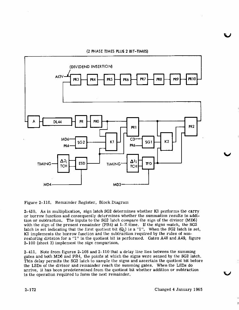
(2 PHASETIMES PLUS2 BIT-TIMES)
(DIVIDEND INSERTION) J
AI3
DL44
MD4
TIMING_
MD3
Figure 2-110. Remainder Register, Block Diagram
2-410. As in multiplication, sign latch SG2 determines whether K1 performs the carryor borrow function and consequently determines whether the summation results in addi-tion or subtraction. The inputs to the SG2 latch compare the sign of the divisor (MD6)with the sign of the present remainder (PR4) at 1-Z time. If the signs match, the SG2latch is set indicating that the first quotient bit (Qi) is a "1". When the SG2 latch is set,K1 implements the borrow function and the subtraction required by the rules of non-restoring division for a "1" in the quotient bit is performed. Gates A48 and A49, figure2-100 (sheet 3) implement the sign comparison.
2-411. Note from figures 2-108 and 2-110 that a delay line lies between the summinggates and both MD6 and PR4, the points at which the signs were sensed by the SG2 latch.This delay permits the SG2 latch to sample the signs and ascertain the quotient bit beforethe LSDs of the divisor and remainder reach the summing gates. When the LSDs doarrive, it has been predetermined from the quotient bit whether addition or subtractionis the operation required to form the next remainder.
2-172 Changed 4 January 1965
2-412. Operationof the PR2adder-subtractor is almost identical to that of the PR1circuit. TheA1 i tratch provides the timing signal for the TFD latch which gates thedivisor (D) to the PR2 summing gates. The SG1 latch forms and stores the secondquotient bit Qi+l (discussed later) in the bit time following formation of Qi. The secondquotient bit then conditions the K2 latch to borrow, if a "1", or carry if a "0". Thus theaddition or subtraction necessary to form the second remainder is predetermined beforethe LSD bits arrive.
2-413. The second quotient bit (Qi+l) is formed in the SG1 latch by comparing the signof the shifted remainder (2-1 bit before the shift) with the carry or borrow into the sign
position. If the shifted remainder sign, sensed at PR6, and the carry or borrow areboth "l's" or both "O's" the Qi+l bit is a "1", otherwise it is a "0". The comparison isaccomplished by gates A43 and A44, figure 2-100 (sheet 3). Both the carry and theborrow into the sign position are represented by one signal, CD.
2-414. As the present remainder is shifted through the remainder register, two latches(CD and BD) keep running accounts of both the carry and borrow conditions which wouldoccur if the divisor were being added to or subtracted from the shifted present remain-der. However, no actual sum or difference is computed at this point. The CD and BDlatches are shown at the lower right of figure 2-100 (sheet 3). As implied by the signalnames, the CD latch stores the carry and the BD latch the borrow. The conditions whichresult in carries andborrows are given in the add-subtract truth table, figure 2-85; tocorrelate these conditions to the divide circuits, substitute PR6 and MD7 for AI4 and B
respectively, in the truth table.
2-415. Notice that the CD and BD latches form all borrows and carries; the timing
signals which select the carry or borrow condition into the sign position as the one tobe compared are applied to gates A43 and A44 (upper left). The timing is such that thedesired carry or borrow is formed simultaneously with the first quotient bit in SG2.This bit determines whether the carry or borrow will be used. However, only the out-
puts of the CD (carry) latch are routed to gates A43 and A44. If the borrow is to be used(SG2 = 1) the content of the BD latch is transferred into the CD latch. Thus, when thesecond quotient bit is formed during the following bit time, the output of the CD latchrepresents the borrow instead of the carry. Consequently, the appropriate function isrepresented at the sensing gates.
2-416. When the complete quotient has been formed, the quotient register is altered toform the PQ register described in paragraph 2-364. This is the same three phase-timeregister used to circulate the results of multiplications and it will now be used to circu-late the result of the division.
2-417. During the last iteration of the division process, the two LSD quotient bits enterthe quotient register through the MR1 latch. As the last bit enters MR1, the phasecounter is set to the third phase condition. This substitutes the output of the Q1 latchfor Q7 at the input to the Q8 latch. Thus latches Q2 through Q7 are bypassed and thefinal quotient enters the Q8 latch with the same timing as final product insertion at theend of a multiplication. The two low-order bits of the quotient are both "O's" whichwere present in latches MR2 and Q1 when the register was altered. Switching the phasecounter to phase three also adds channel two of delay line DL31 and the PQR latch to theregister and switches the input to DL44 from Q9 to PQR. This completes the circulationpath of the PQ register. As in multiplication, the QSD latch provides an output to theArithmetic Element from which the quotient may be read.
"_._z /
Changed 4 January 1965 2-173

2- 418. DELAY LINES.
2-419. Two ultrasonic delay lines (DL31 and DL44) are utilized by the Arithmetic and
Multiply-Divide Elements of the computer. The operation of both delay lines is identical
except for the delay duration. A delay line with an associated driver, sense amplifier,and logic circuits which feed or retrieve delay line data is shown in figure 2-111.
DELAY LINE
30.207 USEC OR
43.390 USECSENSE
AMPLIFIER
*FAST-RISING AND GATE
NOTE - REFERTO FIGURES 10-3, 10-4 (SHEET 1), AND10-5 (SHEET 2) FOR DETAILED LOGIC
ZN
WN
XN
¥N
V
Figure 2-111. Delay Line, Simplified Diagram
2-420. A delayline has four channels corresponding to the four clock times at which
data is fed to the delay line. Channel 1 is fed at W clock time, and channels 2, 3, and4 are fed at X, Y, and Z clock times, respectively. As data bits are loaded into a DL31
channel they emerge 16 bit times plus 2 clock times later; channel 1, 2, 3, and 4 data
bits emerge at Y, Z, W, and X clock times, respectively (all 15 bit times later). Data
bits entered into channels 1, 2, 3, and 4 of DL44 emerge at X, Y, Z, and W clock times,respectively (22 bit times later).
2-174 Changed 4 January 1965

2-421. The output of the delay line is fed to four read latches. The read latches are setjust prior to the emergence of each bit "from the delay line and are either reset or notreset according to the nature of the bit from the delay line. The delay line output islogically inverted by the read latches to correspond to the inputs initially fed into thedelay line input gates; the delay line inputs are logically inverted prior to being suppliedto the delay line driver. A "1" fed into the delay line input gates is inverted to feed a"0" into the delay line. The "0" emerging from the delay line sense amplifier does notreset its associated read latch. Thus, the "0" initially read into the delay line is re-inverted. A "1" emerging from the delay line represents a "0" initially fed into thedelay line input gates. Consequently, a "1" from the delay line resets its associatedlatch.
2-422. The delay line driver is conditioned not only by the inverter but also by bufferoscillator not (BON); BON equals "1" during the second half of each clock time. Con-sequently, when the inverter output is a "1", the delay line is not actually pulsed untilthe second half of the conditioning clock time. Therefore, the delay line output is onlyone-half of a clock time in width; for this reason fast rising AND gates are used with theread latches.
2-423. VOTING ELEMENT.
2-424. In the breadboard model II computer, the Voting Element performs two functions:1) it serves as an interface circuit between the seven modules of the central computerand between the central computer, the memory and external equipment; and 2) it syn-chronizes the three Clock Generators. The ultimate function of the Voting Element,
resolving errors between TMR circuits, is obviated by the simplex nature of the bread-board computer. The Electrical Description of the computer in Section I includes a briefdescription of voter operation in the TMR configuration.
2-425. The Voting Element is composed of a number of voter circuits interspersedthrough the computer. Each voter senses three inputs and produces an output identicalto the majority of its inputs, hence the name "voter". The inputs to each voter areusually supplied by redundant circuits in channels 1, 2 and 3. Since these circuits arenot provided in channels 2 and 3 of the breadboard computer, the corresponding inputsare held to a tie vote, i.e., one "0" and one "1". The input from channel 1 then breaksthe tie and the voter effectively passes the channel 1 input straight through. Power gainand signal isolation are provided through the voter circuit.
2-426. As noted in the preceding paragraph, most of the redundant circuits are missingin the breadboard computer. However, where redundant circuits are provided, thevoters must also be redundant to prevent malfunction of a single voter from causing thecomputer to fail. If a single voter is used, a failure in the voter results in erroneoussignals being fed to all the circuits in the succeeding redundant set. This type of errorcannot be corrected because it appears as a simultaneous failure of all the redundantcircuits in one set. By using redundant voters, a separate voted signal is developed foreach circuit in the succeeding set. (See figure 1-8. ) A malfunction in one voter thenappears as the failure of an individual circuit and is corrected by the next stage ofvoters. The number of redundant voters to be used is determined by the redundancylevel of the circuits which use the voter outputs. If a stage of voters is to feed a tripleredundant circuit, then three voters must be used; only two voters are required to feeda duplex circuit, etc.
Changed 4 January 1965 2-175

2-427. Redundantvoters are usedin only two areas of the breadboardII modelcom-puter, the timing logic for the clock generatorsandat certain points betweenthe com-puter andthe memory. The voters in the clock generatorsare usedfor synchronizationpurposes rather than for error correction andare describedunder Timing Element.Duplexedvoters are usedto vote onsignalswhich are commonto bothduplexmemories.The logic pagesonwhich the voters are mountedare identical to thosefor the TMRcomputerexceptthat no circuits are provided for the voters whichfeed channels2 and3.
2-428. Typical examplesof the two types of voters usedin the computerare shownatA andB in figure 2-112with their equivalentcircuit, C. The operation of both typevoters is essentially the same except for driving capability which is given in the LogicSymbols appendix. Each voter includes a separate AND input for the signals from thethree redundant channels. The clock input of each AND circuit receives a separatelycontrolled "module switching voltage". In the TMR model computers, the moduleswitching voltages may be manipulated by the test equipment as an aid to trouble isola-tion. In the breadboard model II computer, one of the module switching voltages is heldat 0 VDC to simulate a "0" input from one of the missing channels. A "1" input is simu-lated for the other missing channel by providing the normal module switching voltage(+12 VDC) and leaving the signal input to the AND open circuited.
2-429. Each "1" input to the voter causes a current I to flow through the current sum-ruing circuit to the enabled AND circuit. A current of 2I is sufficient to switch the out-put of the summing circuit from a "1" to a "0". When two "l's" are present at the voterinput, the sum of the currents is sufficient to switch the summing circuit output; theinverter output then agrees with the majority input. The voter delays its input by ap-proximately one-third of a clock pulse. Thus a voted signal, unless clocked by a fast-rising AND, may not be sensed until the second clock after it is switched.
2-430. COMPUTER OPERATIONS.
2-431. Descriptions of the computer operations are not provided for the breadboardmodel II computer. This section of the manual will be included in the revisions for thesimplex prototype model computers.
V
2-176 Changed 4 January 1965

AIV5 MOD1
A2V5 MO D1
A3V5 MO D 1
A1PA--I
"I ".--ITI
,,o,,-.k_]
All
A1PAV
A1V5 MOD3_
A2V5 MOD3_
A3V5 MOD3__
A1ACC1---I
"1"-.-J T/_
.o.,-L. -
Be,
A1ACC1V
AIV5 MODI__I
A1PA ,--I._I-
A2V5 MOD lj_j_ 1
"l"'-'[_j I CURRENTSUM
Cg
I NVERTER'--=-- A1
PAV
Figure 2-112. Voter Circuits
Changed 4 January 1965 2-177/2-178

r_

MIB Symbols Volume I
SYMBOL
VOLTS OR CLOCK--I
A-
B-A
C-
O_
--Z
VOLTS
OR C LOCK ---._..__
A--
B--A --
C-- i
Om
E_
F_
AO u
H_
A_
B--A --
C--
D--VOLTS
OR CLOCK--_
E--
F-- A "-_
G--
A
NAME DESCRIPTION
Volts +Clock" A. B' C" D= Z
VOLTS
OR CLOCK
A--
B--
C--
D--A
E--
F--
VOLTS H-_
OR CLOCK
A ,_4
AND Gate
AND Gate, ANDExtenders
A_
B-
C-
D-
E-
F-
G--
._L_
-Z
Heavy line (shown heavy for dis-cussion purposes) indicates anAND extender. Gates connected
by this type line make circuit theequivalent of one large AND gate.
Symbols- 1

Volume I MIB Symbols
j ....
SYMBOL
CLOCK-]
___ICLOCK- I
- A _-_'Z
i
l
BFR I--
$HP
CIi
- C4 --
NAME
AND Gate, Fast-Rising
Buffer Power
Amplifier
Buffer Shaper
Capacitor
DESCRIPTION
Functions like previous AND gateexcept this type has parallel loadresistors to decrease rise time.
Thus, its output can be used oneclock time sooner.
Special circuit used in buffer am-plifier. Provides high power andspecial output levels for operatingdelay lines.
Special circuit used in buffer am-plifier converts sine wave inputto voltage square wave output.
0.22 ufd,
(Four) 25 VDC
Capacitor
Capacitor
Capacitor
2.2 ufd,20 VDC
5.6 ufd,10 VDC
8.2 ufd,6 VDC
v
%./
Symbols- 2

MIB Symbols Volume I
j
SYMBOL
CEF -
t
CGI --
j_
!CLN
CLOCK- IA--
B- DD --
C--
NAME
ULD Type CDR
ComplementaryEmitter- Follower
Clock Gate 1
Clock Gate 2
ULD Type CLN
Dis agree mentDetector
DESCRIPTION
°i°90O11
© - ®
Two emitter-followers connected
back-to-back so that "1" drives
output up and "0" drives outputdown.
Two-input clock gate. Special cir-cuit which AND's two inputs when
"1" and produces a "1" output.Provides special driving levelsfor NSI.
Produces a "1" output with a "1"input. Provides special drivinglevels for NSI.
<
I .8 K ii .8 K
--®
If inputs A, B, and C are at samelevel ("1" or "0") when clocked,
output is a "1". If one is dif-ferent, output is a "0".
Symbols- 3

Volume I MIB Symbols
SYMBOL NAME
C
A+ DD!
I --_
Lmumm
1III
FP I2412J
- II
--B
J DELAY LINE J
._T L_
' IVOLT_-. I
DLXX"I- DLD _' I- I
BON'I"-' II TEST II POINT-_ ' II(Tp) II I
BON_" |Fi2 ._ " "--R-- '1
SIO .I j 2412 i ,
rESTPOINT(TP)
J
DisagreementDetector Inverter
Delay Line
Delay Line Driver
Delay Line SenseAmplifier
DESCRIPTION
Circuit consists of a DDI type ULDand flat pack. Output B is inverseof input A. Input C is a moduleswitching control voltage.
Input "l's" appear at output as volt-age pulses after a specified delaytime. Delay time in usec specifiedby symbol "DL XX" at input toDLD. ("XX"= 31 or 44.)
Circuit consists of: DLD type ULD,resistor R, and half of a flat pack.Delay line driver circuit gatesdrive pulses (BON) into delay linewhen DL XX = "1". ("XX" = 31 or44.)
Amplifies voltage pulses from delayline and converts to "l's".
k.J
Symbols- 4

MIB Symbols Volume I
_,._j/
SYMBOL NAME DESCRIPTION
EDI0--
EDII--
EDI2--
EDI3--
EDI4--
EDI5 --
EDI6--
EDI7--
CR--
EDE--
ED -ED OUT
E CLOCK --'-I-EDE
E
I
I CLOCK _-TCV---s
CR--
- E OUT
-I OUT
-EDI
FP
2412
Error Detector
(Memory)
EI Driver (Memory)
Flat Pack
When memory is addressed, an
"up level" is supplied to the CRinput causing ED OUT = "1". A
loss of this "up level" forcesED OUT to "0". Inputs EDI 0
through EDI 7 forces ED OUT to"0" if more than one input is
selected. Threshold voltage on
EDE input rises when two or more
EI voltage sources are selected,thus forcing ED OUT to "0".
Consider EI driver as two separateunits. E is a voltage source and Ia constant current source. If in-
puts A and B are "l's" when Eclock is present, an output occursat E OUT and EDE. If inputs Aand B are "l's" when I clock is
present, an output occurs at I OUTand EDI. TCV controls amount of
current flow through I OUT. CR
is a current return path which isconnected to ground through an
externally provided resistor. Aand B are essentially ANDed to-
gether. When B is not connected,A is the controlling input.
A pair of transistors mounted in aULD location.
Symbols- 5

Volume I MIB Symbols
SYMBOL NAME DESCRIPTION
Dimm
"-t" Hc'_T--r
I CLNjIL____-:J
-- 1Al_-
._1 IA2 -
TESTPOINT (TP)--- IAm
B-ID --E
C-
D-
High CurrentInverter
m
n
CLOCK 2_
MCD-I
Inverter
Inverter AmplifierType 1 or Type 2
Inhibit DriverCircuit
Memory ClockDriver 1
Circuit consists of ULD types HCI
and CLN. Output isthe inverse
of inputand can drive twenty AND-
gate inputs.
The inverter performs logical andelectrical inversion. An open
input is interpreted as a "0".Where inverter outputs are ORedtogether, an inverter producinga "0" output takes precedence.
Special circuit used only in bufferamplifier. Performs electricalinversion and level shifting.
Produces current pulse at E coin-cident with clock 2 when one or
both signals of both signal pairs(A, B) and (C, D) are "O's". Usedto cancel Y selection current for
planes in which "O's" are to bestored when writing "l's" intomemory. If both signals in eitherpair (A, B) or (C, D) are "l's",output is inhibited allowing a "1"to be written into memory plane.Output current is varied withtemperature of memory array byTCV input. Clock 1 prevents thecircuit from drawing current whenmemory is not being operated.
When both inputs are "l's", theMCD-1 produces a 3.5 usec outputpulse coincident with the fall timeof the first input disabled.
v
Symbols- 6
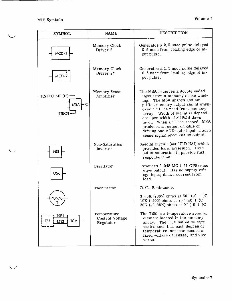
MIB Symbols Volume I
SYMBOL NAME DESCRIPTION
I- MCD-2 --
--MCD-2 -
TEST POINT (TP)'____
MSA -- C
- ISTROB _
i.,
OSC --
r.... _. TSE1
I TSE 1TSE2'II__ __.I
TCV ,-
Memory ClockDriver 2
Memory ClockDriver 2*
Memory Sense
Amplifier
Non- Satur at ingInverter
Oscillator
Thermistor
TemperatureControl Voltage
Regulator
Generates a 2.5 usec pulse delayed
0.5 usec from leading edge of in-
put pulse.
Generates a 1.5 usec pulse delayed
0.5 usec from leading edge of in-
put pulse.
The MSA receives a double ended
input from a memory sense wind-
ing. The MSA shapes and am-
plifies memory output signal when-
ever a "I" is read from memory
array. Width of signal is depend-
ent upon width of STROB downlevel. When a "i" is sensed, MSA
produces ml output capable of
driving one AND-gate input; a zero
sense signal produces no output.
Special circuit (not ULD NSI) whichprovides logic inversion. Heldout of saturation to provide fast
response time.
Produces 2.048 MC (+51 CPS) sine
wave output. Has no supply volt-
age input; draws current from
load.
D.C. Resistance:
3.85K (+385) ohms at 50 : (+0.1)C
10K (+200) ohms at 25 ° (+0.1 _:)C30K (±2.85K) ohms at 0 _ (±0.1)C
The TSE is a temperature sensing
element located in the memory
array. The TCV output voltage
varies such that each degree of
temperature increase causes a
fixed voltage decrease, and vice
versa.
Symbols- 7

Volume I MIB Symbols
SYMBO L NAME DESCRIPTIONm.
F_
E
A--
B - TMV - Z
C-
V_
A- VSG r--C
MCL
MCN
ULD Type TMV
ULD Type VI
Variable DelayStrobe Gate
Output Z is inverse of majority ofinputs A, B, and C, when D, E,and F are all at +12 VDC. Switch-
ing D, E, or F to zero voltseffectively forces a "0" at A, B,or C, respectively. This featureis used for module switching.
Output is inverse of input and iscapable of driving ten AND-gateinputs.
Input pulse at A is delayed in theVSG and provides a down-levelpulse at C. C is inhibited whenB is a "1". MCL and MCN are
used for marginal checkingmemory performance. Advancedstrobe is performed by groundingMCN, and delayed strobe byapplying +6 VDC to MCL; duringnormal operation these inputs areopen circuited.
Symbols-8

SecondLevel Logic Symbols VolumeI
SYMBOL NAME
DL X× I---
XX = DELAY LINE TIMEIN MICROSECONDS
A-
L
i
B--
Delay Line
--G
--H
Latch
DESCRIPTION
The delay line circuit consists of aglass delay line, a delay linedriver, and a delay line sense am-plifier.
A "1" at the input is delayed by theamount of time indicated on the
symbol.
A bistable storage device which canbe operated by "l's" (on input Aor B) or by "O's" (on inputs C, D,Eor F). Inputs A and B arenormally "0" and are called "1"drive inputs. Inputs C, D, E, andF are normally "1" and are called"0" drive inputs. A "1" at A willproduce a "1" at G. The "1" atG will remain irrespective ofconditions at A until one of theother inputs is driven. In similarfashion, a "1" at B produces a "1"at H. A"0"atCor Dproducesa"1" at G; a "0" at E or F producesa "1" at H.
C DI
r i_.--g .......... "=1
A=J '- I
I--_ A - I :: I
LATCHI
I 'I ;, 1
! ,B; IL_
G
H
E F
_,..J
Symbols- 9

Volume I Second Level Logic Symbols
SYMBOL
"0" (Zero Drive)
"I "-_"o" (A)
"O"fl TCH t"l"
,,o,,._L_,, 1,,
NAME
Tratch
(Exclusive 0)
Voter
DESCRIPTION
A tristable storage device whichwill assume one of three stable
states. The output will containonly one "0" at any time. A "1"on any input causes the outputdirectly opposite that input to bea "0". The zero drive going to"0" forces (A) to a "0".
mluml J
"I "-_
II
_(ZERO DRIVE)
I
I
II
Voter output represents majorityof three inputs, two of whichare not shown. This logic symbolrepresents either of two circuits:1) the TMR voter which is com-posed of one TMV and one VIunit logic device; and 2) the TMRpower voter which is composedof one TMV, one HCI and oneCLN unit logic device. The TMRvoter can drive ten 1.5K AND
gates, and the TMR power votercan drive twenty 1.5K AND gates.
V
V
k9
Symbols-10 Changed 4 January 1965

k.._/
GLOSSARY
SYMBOL
A
AB
Accumulator
ADD
AND
AXON thru AXTN
A1 thru A8
A9
AlAN thru A8AN
A9PADN
ACC0
ACC1
AI0
AI1 thru AI4
AX00N thru AXTON
AYON thru AY7N
AY00N thru AY70N
B
Volume I
DEFINITION
Bit Gate Generator Latch A, used to decode even num-bered bit gates during W and X clock times
Bit Gate Generator Latch AB, used to control the ALatch
Circuit which consists of an adder and a register; theoutput of the adder is stored in the register
Programmed Add operation
Latch which decodes logical AND operation
Inverse low order X axis decoded memory addresses,octal 0 thru 7
Address Register Latches 1 thru 8
Address Register Latch 9, used to select the ResidualMemory Sector
Zero output of Address Register Latches 1 thru 8
Inverse signal generated to select the Residual Memory
Latch in the Accumulator-Register which stores serialoutput of 44.5 microsecond delay line
Delay latch in Accumulator- Register
Latch in Accumulator-Register which stores serial out-put of 31 microsecond delay line
Delay latches in Accumulator Register
Eight inverse high order X axis decoded memory ad-dresses, octal 0 thru 7
Inverse low order Y axis decoded memory addresses,octal 0 thru 7
Eight inverse high order Y axis decoded memory ad-dresses, octal 0 thru 7
Accumulator latch which controls one of the data entriesto Accumulator
Glossary-i

Volume I
SYMBOL
b
BD
BFR DVR
BFR SHP
BO
BRAO
BRBO
BO1 thru BO3
BOT1 thru BOT3
BRA1 thru BRA14
BRA14P
BRB1 thru BRB14
BRB14P
C
CBRN
CD
CDS
CEF
Channel
CKP
CLA
C LTR
DEFINITION
Multiplier
Latch used during divide to generate the borrow of twicethe remainder minus the divisor
Buffer Driver
Buffer Shaper
Buffered Oscillator Signal
Latch which gates Buffer Register A outputs into mem-ory inhibit drivers
Latch which gates Buffer Register B outputs into Mem-ory Inhibit Drivers
Outputs of Buffer and Oscillator circuit for clock timingin channels 1 thru 3
Intermediate outputs of Buffer and Oscillator circuit forclock timing in channels 1 thru 3
Buffer Register A Latches 1 thru 14
Special output of memory parity bit for test equipment
Buffer Register B Latches 1 thru 14
Special output of memory parity bit for test equipment
Arithmetic Element Carry Latch
Inverse signal generated to clear the Buffer Registers
Latch used during divide to generate the carry of twicethe remainder plus the divisor
Change Data Sector Register Latch- used during a HOPor Change Data Sector instruction
Complementary Emitter Follower
Group of pages which contain logic circuits. Computerconsists of three TMR channels and two simplex chan-nels
Check Parity Latch
Programmed Clear and Add operation
Clear Transfer Register Latch
V
%.2
Glossary-2

SYMBOL
CNC
COC
Computer Cycle
CST
CSTN
DATAV
Data word
DIN
DIV
DLD31B, DLD44B
DL31
DL44
DL31SA
DL44SA
DMA
DMB
DM0
DM1
DM2
DM3
DSS
DS1 thru DS4
Volume I
DE FINITION
Check No Current Latch
Check On Current Latch
A-1-Y time to C-14-Y time
Signal which permits single step operation of the com-
puter
Inverse signal from external equipment used to control
computer single step operation
Normal data input from external equipment
28 bits including two parity bits
Special data input from LTE used to control memoryload and verify operations
Programmed divide operation
Outputs of delay line driver circuits to delay lines
Input to the 31 microsecond Delay Line Driver
Input to the 44.5 microsecond Delay Line Driver
Output of the 31 microsecond Delay Line Sense Amplifier
Output of the 44 microsecond Delay Line Sense Amplifier
An inverter output indicating that the data is from an
even numbered memory module
An inverter output indicating that the data is from anodd numbered memory module
Tratch output indicating that the low order position ofthe Data Module Register is a zero
Tratch output indicating that the low order position of
the Data Module Register is a one
Second position of the Data Module Register
Third position of the Data Module Register
Data Sector Serialized Latch - gates data sector bitsinto the Data Sector Register for HOP or ChangeData Sector instruction
Data Sector Latches 1 thru 4
Glossary-3

Volume I
DSlM
DS2M
DTM
DUPDN
DUPIN
EAC
EADM
EAIM
EAM
EAP
EBC
EBDM
E BIM
EBM
EBP
EDAC
EDBC
SYMBOL DE FINITION
First Data Sector Register Modified Latch used duringan EXM instruction
Second Data Sector Register Modified Latch used duringan EXM instruction
Timing latchin the Multiply-Divide Element
Tratch output indicating that the memory is in the sim-plex mode of operation for data
Tratch output indicating that the memory is in the sim-plex mode of operation for instructions
An inverter output indicating a failure in an even num-bered module due to a half-select error in either a
data or instruction cycle
Latch indicating a failure in one of the even numberedmemory modules during an operation cycle
Latch indicating a failure in one of the even numberedmemory modules during an instruction cycle
Latch which indicates an error in even memories
Output from Buffer Register A parity check logic,error signal
An inverter output indicating a failure in an odd num-bered module due to a half-select error in either an
operation or instruction cycle
Latch indicating a failure in one of the odd numberedmemory modules during an operation cycle
Latch indicating a failure in one of the odd numberedmemory modules during an instruction cycle
Latch which indicates error in odd memories
Buffer Register B parity check logic, error signal
Latch indicating a failure of one of the even numberedmemory modules as detected by the half-select cur-rent monitors during an operation cycle
Latch indicating a failure of one of the odd numberedmemory modules as detected by the half-select cur-rent monitors during an operation cycle
%g
Glossary- 4

k._/SYMBOL
EDmX, EDmY
EIAC
EIBC
EMDN
ESD
EXM
EXMD
FCD
FMDN
FSA
FSB
G1 thru G7
HALTV
HOP
HOY
HOPCI
HPI
IMA
IMB
Volume I
DE FINITION
Output of half-select current Error Detector circuit inmemory
Latch indicating a failure of one of the even numberedmemory modules as detected by the half-select cur-rent monitors during an instruction cycle
Latch indicating a failure of one of the odd numberedmemory modules as detected by the half-select cur-rent monitors during an instruction cycle
Zero during a Multiply operation if delta 2 equals eight,zero during Divide
Latch used as delta 2 during either Multiply operation,or as twice the divisor during Divide
Latch which decodes the Execute Modified instruction
Execute Modified Instruction Delayed Latch
Signal which forces a Clear And Add operation into theOperation Code Register
Zero during a Multiply iteration if delta 1 equals four,zero during Divide
Latch indicating that a failure has been sensed by thehalf-select current monitor in an even numberedmodule
Latch indicating that a failure has been sensed by thehalf-select current monitor in odd numbered module
Bit Gate Generator Latches 1 thru 7
External signal used to control program initiation
Latch which decodes HOP instruction
Latch set by Multiply And Hold or Multiply
Latch which generates the HOP constant for storageduring an Interrupt operation
Latch which generates the HOP constant during odd bittimes
An inverter output indicating that the instruction is froman even numbered memory module
An inverter output indicating that the instruction is froman odd numbered memory module
Glossary- 5
VolumeI
SYMBOL
INHBS
Instruction Cycle
Instruction Word
INT
INTA
INTB
INTCV
INV
ISS
IM0
IMI
IM2
IM3
IS1 thru IS4
JBN
K1
K2
M
MAO
MB
MBO
MFF
DEFINITION
Signal which inhibits strobing of the Memory Sense Am-plifiers
A-1-Y time to B-1-Y time
13 instruction bits + I parity bit
Latch indicating an Interrupt
First Interrupt Interlock Control Latch
Second Interrupt Interlock Control Latch
External signal which indicates that program should beinterrupted
Inverter
Instruction Sector Serialized Latch - gates instructionsector bits into the Instruction Sector Register for aHOP instruction
Tratch output indicating that the low order position ofthe Instruction Module Register is a zero
Tratch output indicating that the low order position ofthe Instruction Module Register is a one
Second position of the Instruction Module Register
Third position of the Instruction Module Register
Instruction Sector Latches 1 thru 4
Partial decode of Shift instruction
Latch used as carry or borrow by PR1
Latch used as carry or borrow by PR2
Multiplicand
Latch output which gates Buffer Register A output intothe Transfer Register
Multiplier Bit
Latch output which gates Buffer Register B output intothe Transfer Register
An inverter output indicating computer operation ineither Memory Module four or five
Glossary-6

Volume I
SYMBOL
MmCRX
MmCRY
MmEDEX, MmEDEY
MmTCV
MmTSE
Module
MOP
MPH
MPY
MSS
MTT
MZO
MOSYNC
M1SYNC thru M7SYNC
MD0 thru MD7
MmEDI 0 thru
MmEDI 7
MmEDIY 0 thruMmEDIY 7
MmHEY0 thruMmHEY7
MmHIY0 thru
MmHIY7
MmINH1 thruMmINH14
DEFINITION
Memory Module m X Address Driver current return
Memory Module m Y Address Driver current return
Voltage monitor output from memory address drivers to
half-select current Error Detector circuit in memory
Memory Module m Temperature Controlled Voltage
Memory Module m Temperature Sense Element
Group of circuits on a page(s) performing the same orrelated functions. Seven modules in each of the threeredundant channels
Signal indicates a read or store Memory operation
Programmed Multiply and Hold operation
Programmed Multiply operation
An inverter output indicating computer operation ineither Memory Module Six or Seven
An inverter output indicating computer operation ineither Memory Module Two or Three
An inverter output indicating computer operation ineither Memory Module Zero or One
Start signal to Memory Module 0 which initiates a mem-ory cycle
Start signal to Memory Module 1 thru Memory Module7 which initiates a memory cycle
One output of latches in the Multiplicand-Divisor Register
Voltage monitor output from memory address drivers to
half-select current Error Detector circuit in memory
Special outputs of Y memory address drivers for currentmonitoring by Error Detector circuits
Memory Module m High Y Address Driver voltagesources, octal 0 thru 7
Memory Module m High Y Address Driver currentsources, octal 0 thru 7
Memory Module m Inhibit Drive 1 thru 14
Glossary-7

Volume I
SYMBOL
MmLEX0 thruMmLEX7
MmLEY0 thruMmLEY7
MmLIX0 thruMmUX7
MmLIY0 thruMmLIY7
MmRDP1 thruMmRDP3
MmS1E0 thruMmS1E7
MmSlI0 thru MmSII7
MmSA1 thru MmSA14
MmSL1A thru MmSA14A
MmSL1B thru MmSL14B
MmSOE0 thru MmSOE7
MmS010 thru MmS017
MmSTROB
MmSTRP1 thruMmSTRP3
MR0 thru MR2
N
NSI
NU
OC
Operand
Glossary-8
Memory Modulesources, octal
Memory Modulesources, octal
Memory Modulesources, octal
Memory Modulesources, octal
Memory Module
DE FINITION
m Low X Address Driver voltage0 thru 7
m Low Y Address Driver voltage0 thru 7
m Low X Address Driver current0 thru 7
m Low Y Address Driver current0 thru 7
m Read Pulse 1 thru 3
Memory Modulesources, octal
Memory Modulesources, octal
Memory Module
Memory Module
Memory Module
Memory Modulesources, octal
Memory Modulesources, octal
Memory Module
Memory Module
m Syllable 1 Address Driver voltage0 thru 7
m Syllable 1 Address Driver current0 thru 7
m Sense Amplifier, outputs 1 thru 14
m Sense Lines 1 thru 14, A end
m Sense Lines 1 thru 14, B end
m Syllable 0 Address Driver voltage0 thru 7
m Syllable 0 Address Driver current0 thru 7
m Sense Amplifier Strobe pulse
m Store Pulses 1 thru 3
Latches in the Multiplier, Quotient, Product-QuotientRegisters
Letter symbol suffix, when added to signal name, indi-cates a NOT condition
Non- Saturating Inverter
Latch in Automatic HOP Save Circuit
Latch which generates the HOP constant during evenbit times
Data used in arithmetic operation

SYMBOL
Operation Cycle
OP1 thru OP4
P
P
P
PA
PAD
PAR
Parity bit (odd)
PB
PC
PDD
PIO
Plane
POD
PQR
PR
PW_R RET
PIN
P2N
P3N
PAE1 thru PAE5
PAE6N
Volume I
DEFINITION
B- 1- Z time to C- 14- Y time
Operation Code Register Latches 1 thru 4
Letter symbol suffix, when added to signal name, indi-cates power amplification
Latch in clock generator timing logic
Product of a multiply operation
Phase Generator Latch A
Phase A Delayed Latch
Latch which generates the final parity bit for transferto the Memory Buffer Register
A bit, when added to computer word or syllable, makestotal number of bits an odd number
Phase Generator Latch B
Phase Generator Latch C
Parity Generator Latch Delayed
Decoded Process Input Output operation
All cores in a memory module which store the same bitposition in a syllable
Parity Generator Latch
Latch in the Product-Quotient Register
Latch in the Partial Product-Remainder Register
Power return
Zero during first iteration of Multiply, Multiply andHold, and Divide
Zero during second and remaining iterations of Multiply,Multiply and Hold, and Divide
Set to zero after final iteration of Multiply, Multiplyand Hold, and Divide
Buffer Register A parity check logic, even inverters1 thru 5
Buffer Register A parity check logic, even inverter 6
Glossary- 9

VolumeI
SYMBOL
PAO1 thru PAO12
PBE1 thru PBE5
PBE6N
PBO1 thru PBO12
PRO thru PRI0
Q
Q1 thru Q9
Q8D
R
RAC
RD
RDM
RECN
RED
REI
RUN
S
SAPO
SBRX
SBRY
SBRZ
Sector
DEFINITION
Buffer Register A parity check logic, odd inverters 1thru 12
Buffer Register B parity check logic, even inverters 1thru 5
Buffer register B parity check logic, even inverter 6
Buffer register B parity check logic, odd inverters 1thru 12
Latches In Product-Remainder Register
Latch in clock generator tinting logic
Latches in the Quotient, Product-Quotient Register
Q8 Delayed Latch
Latch in clock generator timing logic
Latch which controls recirculation of contents of theAccumulator- Register
Signal indicates a Read Memory operation
Signal from latch which controls reading from the mem-ory
Manual reset for error detect logic
Read Data Latch
Read Instruction Latch
Latch which is externally controlled and starts the com-puter operating
Latch in clock generator timing logic
Partially decoded SHF and PIO operations
Signal generated to transfer the contents of the TransferRegister into the Buffer Registers at X time
Signal generated to transfer the contents of the TransferRegister into the Buffer Registers at Y time
Signal generated to transfer the contents of the TransferRegister into the Buffer Registers at Z time
Preselected area of memory module for memory
addressing
V
Glossary- i0

SHF
SINK
SLD
SMDN
SRTR
SS
SSF
SSFSN
STMD
STO
STP
SUB
Syllable
SYNC
$4
SG1
SG2
SYLON
SYLC1
TA
TBC
SYMBOL
Volume I
DEFINITION
Programmed shift operation; output of the SHF Opera-tion Decoder circuit
Latch which generates the initial start memory signal
Syllable Delayed Latch
Zero during a Multiply operation if delta 2 equals sixteen
Shift Right Transfer Register Latch
Decoded octal address 776 or 777
Decoded operand address 775
Decoded operand address 775 or 777, used to developSSF
Latch causing data from the Multiplicand Register to bestored
Programmed Store operation, output of STO OperationDecoder circuit
Latch in the Multiply- Divide Timing Circuit
Programmed Subtract operation
Half of a computer word; half of a memory module
Latch which develops the memory start signal whengated with the Memory Module Register outputs
Latch which controls selection of the Memory Sector
Latch which stores the sign of delta 1 during eitherMultiply operation, or the lower order quotient bitduring Divide
Latch which stores the sign of delta 2 during eitherMultiply operation, or the higher order quotient bitduring Divide
Inverse outputs of latch which controls reading or writingof syllable zero or syllable one in the memory
Instruction Syllable Control Latch
Latch which transfers the address in the Transfer
Register to the Address Register
Timing latch which gives output from B-3-Y to A-1-Y
Glossary- 11
Volume I
SYMBOL
TBR
TFD
TIME
TLC
TM
TMDM
TMI
TNZ
TILE
TRS
TTL
TTT
TRI thru TRI3
TRID
TR3D
TR6D
TR9D
TRI2D
UACC0
UTR
V
VIN
DEFINITION
Latch which causes a transfer of data from the Buffer
Register to the Transfer Register
Latch used as delta 1 during either Multiply operation,or as the Divisor during divide
Latch which indicates when the parity check logic shouldbe sampled for an error condition
Latch indicating two simultaneous memory errors, anabort condition
Timing Latch in the Multiply-Divide Element
Zero during a Multiply iteration if delta 1 equals two
Programmed Transfer Minus operation
Programmed Transfer Non-Zero operation
Programmed Transfer operation
Transfer Register Serial Output Latch
Latch used to gate data transfers between PQ Registerand Accunmlator- Register
Signal indicating no transfer operation
Transfer Register Latches 1 thru 13
Transfer Register Latch 1 Delayed
Transfer Register Latch 3 Delayed
Transfer Register Latch 6 Delayed
Transfer Register Latch 9 Delayed
Transfer Register Latch 12 Delayed
Signal from latch which specifies use of the InstructionCounter contents for the next instruction address
Signal from latch which specifies use of operand addressto replace instruction address in Instruction Counterduring any Transfer operation or HOP operation
Letter symbol suffix, when added to signal name, indi-cates a voted output
Voter Inverter
Glossary-12

VolumeI
SYMBOL
Voter
VOY
V1
V3
V4MOD1 thru V4MOD7
V20
WDA
WF
WN
Wl thru W8
XDA
XF
XN
XOR
Xl thru X8
YDA
YF
YN
Y1 thru Y8
ZDA
ZF
ZDHN
ZDLN
ZER
ZN
Z1 thru Z8
DE FINITION
Circuit with three 2-state inputs; output is the same asmajority of inputs
Latch which decodes Divide or Multiply instructions
+6 VDC
-3 VDC
+6 VDC, module switching
+20 VDC
W Clock Pulse Driver to Data Adapter
W Clock feedback signal to other Clock Drivers
Inverse signal of Wl thru W8
W Clock Pulse Drivers 1 thru 8
X Clock Pulse Driver to Data Adapter
X Clock feedback signal to other Clock Drivers
Inverse signal of Xl thru X8
Programmed Exclusive OR operation
X Clock Pulse Drivers 1 thru 8
Y Clock Pulse Driver to Data Adapter
Y Clock feedback signal to other Clock Drivers
Inverse signal of Y1 thru Y8
Y Clock Pulse Drivers 1 thru 8
Z Clock Pulse Driver to Data Adapter
Z Clock feedback signal to other Clock Drivers
Zero during a Multiply iteration if delta 2 equals zero
Zero during a Multiply iteration if delta 1 equals zero
Latch which checks for non-zero condition of theAccumulator contents
Inverse signal of Z1 thru Z8
Z Clock Pulse Drivers 1 thru 8
Glossary-13/14

V
4,j
V

Volume I
LJ
INDEX
A
Accumulator register ..... 2-6, 2-128Address register ......... 2- 4, 2- 93Add- subtract (A/S) circuit ...... 2-125Add- subtract logic ........ 2- 8, 2-126And latch .................. 2-17Arith control ............... 2-119
Arithmetic element ........ 2-4, 2-117
B
B latch ................... 2-125Bit time, identification ......... 2-29Buffer- amplifier ............. 2- 23Buffer registers ............. 2-59
C
Carry (C) latch ............. 2-125Change data sector (CDS) latch... 2-101Clock drivers ............... 2-26Clock generator ............. 2-13Command circuit ....... 2-141, 2-169Computer assemblies ........... 1- 2Computer, general handling ....... 5-5Computer operations .......... 2-176Computer organization .......... 2-1Computer single step (CST)-
gate ................... 2-108operation ............... 2-100
Control circuit ............... 2-29Core array 2-38, 2-40
D
Data control element ...... 2-4, 2-85Data module register .......... 2-4Data sector register ....... 2-4, 2-95Delay circuits .............. 2-110Delay lines ............... 2-174Description-
electrical ................ 1-6structural ............... 1-2
Detectors, disagreement ........ 1-6Division-
arithmetic registers ........ 2-169command circuit .......... 2-169computer method .......... 2-164logic circuits ............ 2-168
D (cont)
nonrestoring method ....... 2-161restoring method .......... 2-161timing circuits ........... 2-169
E
E-I drivers ................. 2-45Equipment, purpose of ......... 1-1Error detectors .............. 2-54Execute modify (EXM) latch ..... 2-101Execute modify delay (EXMD)
latch ................... 2-101
F
Forced clear and add (FCD)gate .................... 2-104
Ferrite core, toroidal .......... 2-32
H
Hi X decoder ................ 2-62Hi Y decoder ................ 2-63HOP-
constant serializer .......... 2-16latch .................. 2-104
save circuit, automatic ...... 2-108
IInhibit driver ................ 2- 51Instructions-
ADD .................... 2-17AND .................... 2-17CDS .................... 2-18CLA .................... 2-20DIV .................... 2-16EXM ................... 2-19HOP .................... 2- 16MPH ................... 2-17MPY ................... 2-16PIO .................... 2-17RSU .................... 2-18SHF .................... 2-18STO .................... 2-17SUB .................... 2-16TMI .................... 2-18TNZ .................... 2-17TRA .................... 2-17XOR .................... 2-17
Changed 4January 1965 Index-1

VolumeI
INDEX (Cont)
I (cont)
Instruction counter ....... 2-4, 2-110Instruction module register ....... 2-4Instruction organization ......... 2-13Instruction sector register .... 2-4, 2-95Interconnection-
Computer - ATOM ........... 3-12Computer- data adapter ....... 3-10Computer --LVDC- ME ........ 3-11
Interface .................... 3-1
Interface listing ............... 3- 2Interrupt control ......... 2-5, 2-105
L
Logic-MIB diagrams ............. 10-1section ................... 1- 2
Logic description-addition (ADD) ............ 2-126and (AND) ............... 2-128clear and add (CLA) ........ 2-126exclusive or (XOR) ......... 2-128reverse subtraction (RSU) .... 2-126subtraction (SUB) .......... 2-126shift (SHF) .............. 2-129
Lo X and Lo Y decoders ........ 2-62
M
Manual, purpose of ............. 1-1Memory-
address decoders ........... 2- 60address drivers ............ 2- 45
buffer register ......... 2-4, 2-59buffer select latches ......... 2-83clock drivers .......... 2-2, 2-44control element ........ 2-2, 2-140element .............. 2- 2, 2- 32error monitors ............. 2- 80
mode and module select .. 2-2, 2-70module registers ........... 2- 74module select control
circuit ................. 2- 74
module select gates ......... 2-77section ................... 1- 2
select and error monitor . . 2-2, 2-77sense amplifier ............ 2- 53sync timing ........... 2-2, 2-69timing and sync select ........ 2-2
Index- 2
M (cont)
Multiplication-arithmetic registers ........ 2-144command circuit .......... 2-143
computation cycle .......... 2-158logic circuits ............. 2-141multiplicand register ....... 2-144multiplier register ......... 2-146partial product register ...... 2- 147phase counter ............ 2-143process ................ 2-137product- quotient register.. 2- 8, 2-144timing circuits ............ 2-142
Multiply-divide element ..... 2- 4, 2-131Multiply formula, derivation .... 2-131
O
Operation code ............... 2-11Operation code register ..... 2- 4, 2- 97Operation decoders ........ 2- 8, 2-101Oscillator .................. 2-15
P
Page assembly ................ 1- 2Parity check circuits ........... 2-80Parity counter ........... 2- 4, 2- 90Phase generator ......... 2-11, 2-29Printed circuit cables ........... 1-2
Program control element .... 2- 4, 2- 91Process input-output (PIO)
gate .................... 2-104
R
Recirculate accumulator
(RAC) latch ............... 2-123Reference designators ........... 1- 2Repair ..................... 9- 1Replacement-
page assembly .............. 9-1memory assembly ............ 9- 5
Run latch .................. 2-105
S
Seven, seven, seven, or seven,seven, six (SS)gate ......... 2-I04

Volume I
INDEX (Cont)
S (cont)
Seven, seven, five (SSF)gate .................... 2-104
Shift and process input- output(SAPO) gate ............... 2-104
Shift (SHF)-gate ................... 2-104LSD-1 ................. 2-129LSD-2 ................. 2-129MSD- 1 ................. 2-131MSD-2 ................. 2-131
Shipment, preparation for ........ 5-3Signal tracing ............... 10- 2Start- stop control ......... 2- 5, 2-105Store multiplicand (STMD)
latch ................... 2-110
Store (STO) gate ............. 2-104Store not (STON) gate ......... 2-104Storage, preparation for ......... 5-1Syllable select ........... 2-4, 2-67
T
Temperature control voltage(TCV) regulator ............. 2-55
Test equipment, special ......... 4-1Test equipment, standard ........ 4-1Time B and C (TBC) latch ....... 2-31Timing element .......... 2-2, 2-13Timing gate generator .......... 2-26Timing logic ................ 2- 24Timing organization ........... 2-11Tools, special ................ 4-1Transfer register .......... 2-4, 2-85Transfer register control
latches ................... 2-88Triple modular redundancy ....... 1-6TTL latch ................. 2-104
Time to transfer (TTT) gate ..... 2-105
U
Use, preparation for ............ 5-1
V
Voters ................ 1-6, 2-175Voting element ........... 2-6, 2-175
W
Word organization ............ 2-10
Changed 4 January 1965 Index-3/4
