a single-cycle mips processor - university of...
TRANSCRIPT

1
Lecture 7
You should all have a lab partner by now
Lab #1 due Jan 30th
HW2 will be released later today, due Feb 2nd.
— We are sure you will like it
Come to section tomorrow, we will review Verilog, which you will be
using in the labs
2
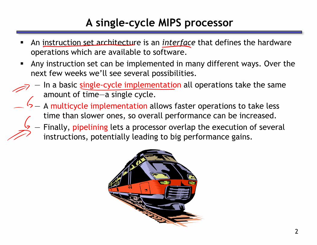
A single-cycle MIPS processor
An instruction set architecture is an interface that defines the hardware
operations which are available to software.
Any instruction set can be implemented in many different ways. Over the
next few weeks we’ll see several possibilities.
— In a basic single-cycle implementation all operations take the same
amount of time—a single cycle.
— A multicycle implementation allows faster operations to take less
time than slower ones, so overall performance can be increased.
— Finally, pipelining lets a processor overlap the execution of several
instructions, potentially leading to big performance gains.

3
Single-cycle implementation
We will describe the implementation a simple MIPS-based instruction set
supporting just the following operations.
Today we’ll build a single-cycle implementation of this instruction set.
— All instructions will execute in the same amount of time; this will
determine the clock cycle time for our performance equations.
— We’ll explain the datapath first, and then make the control unit.
Arithmetic: add sub and or slt
Data Transfer: lw sw
Control: beq

4
Computers are state machines
A computer is just a big fancy state machine.
— Registers, memory, hard disks and other storage form the state.
— The processor keeps reading and updating the state, according to the
instructions in some program.
State
CPU
5
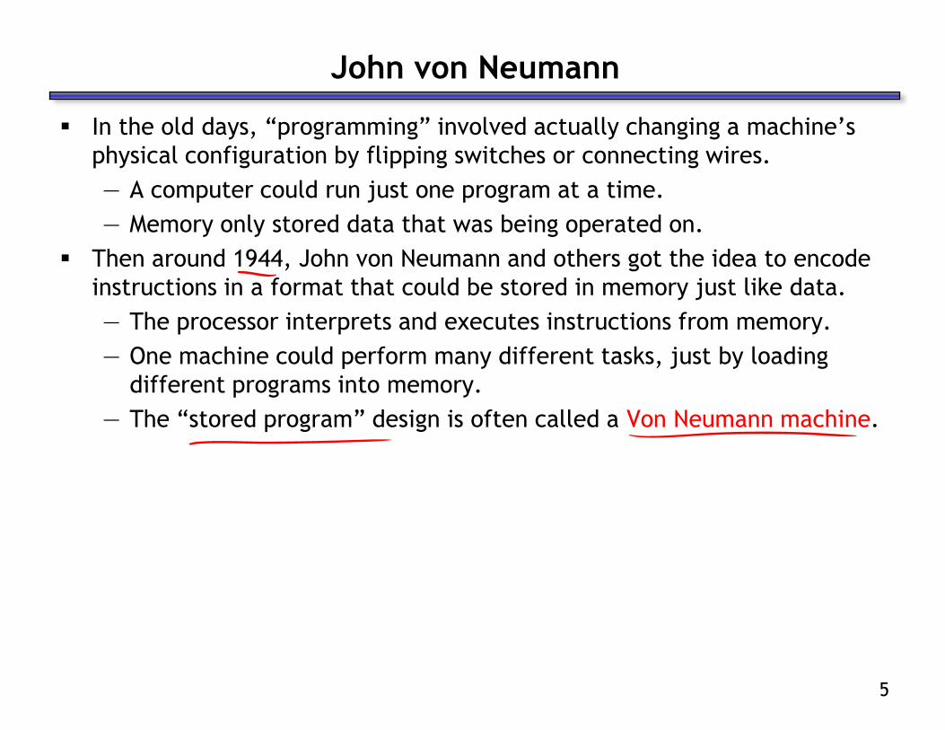
John von Neumann
In the old days, ―programming‖ involved actually changing a machine’s
physical configuration by flipping switches or connecting wires.
— A computer could run just one program at a time.
— Memory only stored data that was being operated on.
Then around 1944, John von Neumann and others got the idea to encode
instructions in a format that could be stored in memory just like data.
— The processor interprets and executes instructions from memory.
— One machine could perform many different tasks, just by loading
different programs into memory.
— The ―stored program‖ design is often called a Von Neumann machine.
6
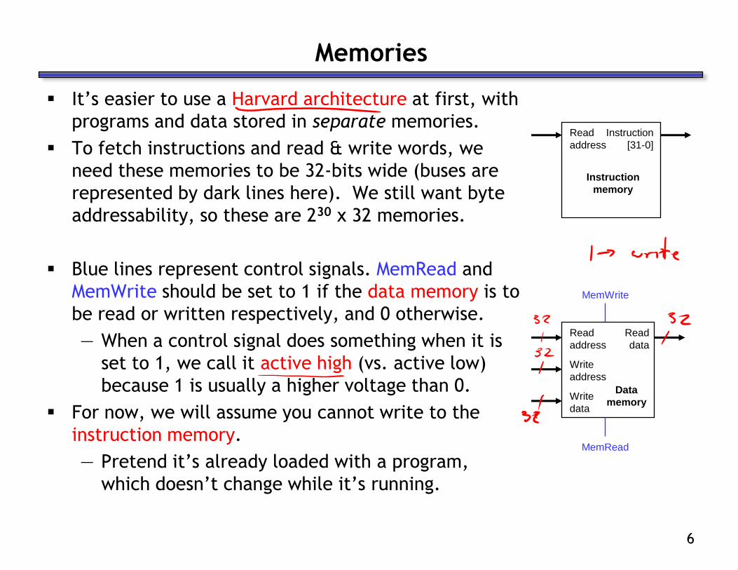
Memories
It’s easier to use a Harvard architecture at first, with
programs and data stored in separate memories.
To fetch instructions and read & write words, we
need these memories to be 32-bits wide (buses are
represented by dark lines here). We still want byte
addressability, so these are 230 x 32 memories.
Blue lines represent control signals. MemRead and
MemWrite should be set to 1 if the data memory is to
be read or written respectively, and 0 otherwise.
— When a control signal does something when it is
set to 1, we call it active high (vs. active low)
because 1 is usually a higher voltage than 0.
For now, we will assume you cannot write to the
instruction memory.
— Pretend it’s already loaded with a program,
which doesn’t change while it’s running.
Read
address
Instruction
memory
Instruction
[31-0]
Read
address
Write
address
Write
data
Data
memory
Read
data
MemWrite
MemRead
7
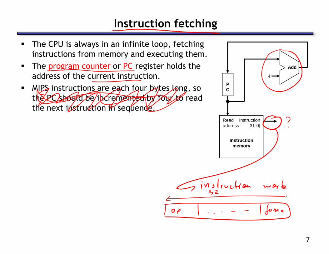
Instruction fetching
The CPU is always in an infinite loop, fetching
instructions from memory and executing them.
The program counter or PC register holds the
address of the current instruction.
MIPS instructions are each four bytes long, so
the PC should be incremented by four to read
the next instruction in sequence.
Read
address
Instruction
memory
Instruction
[31-0]
P
C
Add
4

8
Encoding R-type instructions
Last lecture, we saw encodings of MIPS instructions as 32-bit values.
Register-to-register arithmetic instructions use the R-type format.
— op is the instruction opcode, and func specifies a particular arithmetic
operation (see textbook).
— rs, rt and rd are source and destination registers.
An example instruction and its encoding:
add $s4, $t1, $t2
op rs rt rd shamt func
6 bits 5 bits 5 bits 5 bits 5 bits 6 bits
000000 01001 01010 10100 00000 1000000

9
Registers and ALUs
R-type instructions must access registers and an ALU.
Our register file stores thirty-two 32-bit values.
— Each register specifier is 5 bits long.
— You can read from two registers at a time.
— RegWrite is 1 if a register should be written.
Here’s a simple ALU with five operations, selected by
a 3-bit control signal ALUOp.ALU
ALUOp
Read
register 1
Read
register 2
Write
register
Write
data
Read
data 2
Read
data 1
Registers
RegWrite
ALUOp Function
000 and
001 or
010 add
110 subtract
111 slt

10
Executing an R-type instruction
1. Read an instruction from the instruction memory.
2. The source registers, specified by instruction fields rs and rt, should be
read from the register file.
3. The ALU performs the desired operation.
4. Its result is stored in the destination register, which is specified by field
rd of the instruction word.
Read
address
Instruction
memory
Instruction
[31-0]
Read
register 1
Read
register 2
Write
register
Write
data
Read
data 2
Read
data 1
Registers
RegWrite
I [25 - 21]
I [20 - 16]
I [15 - 11]
Result
Zero
ALU
ALUOp
op rs rt rd shamt func
31 26 25 21 20 16 15 11 10 6 5 0
11
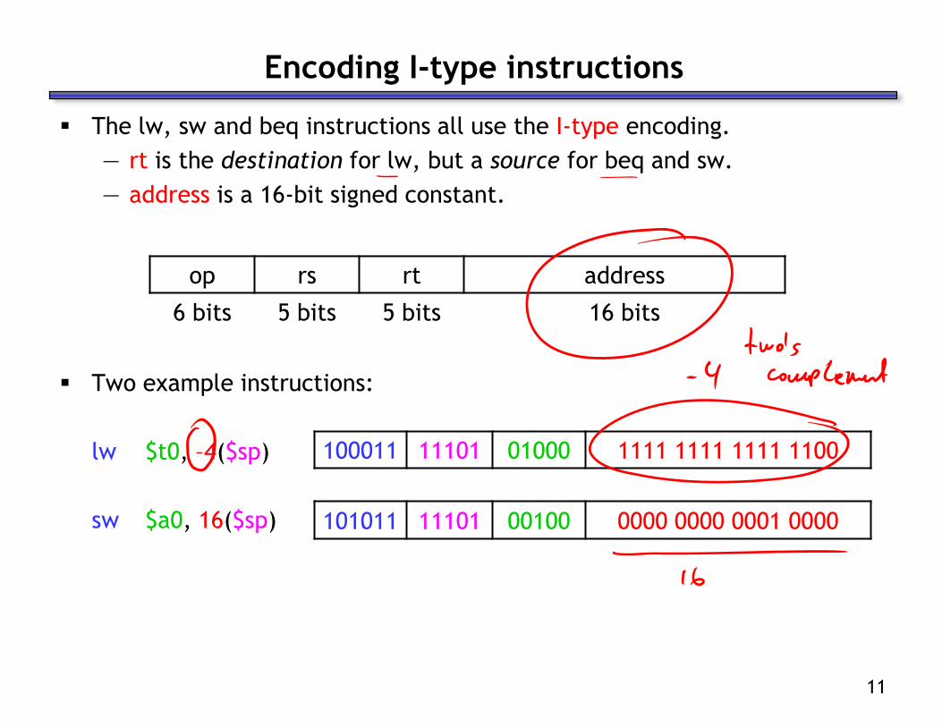
Encoding I-type instructions
The lw, sw and beq instructions all use the I-type encoding.
— rt is the destination for lw, but a source for beq and sw.
— address is a 16-bit signed constant.
Two example instructions:
lw $t0, –4($sp)
sw $a0, 16($sp)
op rs rt address
6 bits 5 bits 5 bits 16 bits
100011 11101 01000 1111 1111 1111 1100
101011 11101 00100 0000 0000 0001 0000

12
Accessing data memory
For an instruction like lw $t0, –4($sp), the base register $sp is added to
the sign-extended constant to get a data memory address.
This means the ALU must accept either a register operand for arithmetic
instructions, or a sign-extended immediate operand for lw and sw.
We’ll add a multiplexer, controlled by ALUSrc, to select either a register
operand (0) or a constant operand (1).
Read
address
Write
address
Write
data
Data
memory
Read
data
MemWrite
MemRead
1
Mux
0
MemToRegRead
address
Instruction
memory
Instruction
[31-0]
I [15 - 0]
I [25 - 21]
I [20 - 16]
I [15 - 11]
0
Mux
1
RegDst
Read
register 1
Read
register 2
Write
register
Write
data
Read
data 2
Read
data 1
Registers
RegWrite
Sign
extend
0
Mux
1
ALUSrc
Result
Zero
ALU
ALUOp
13
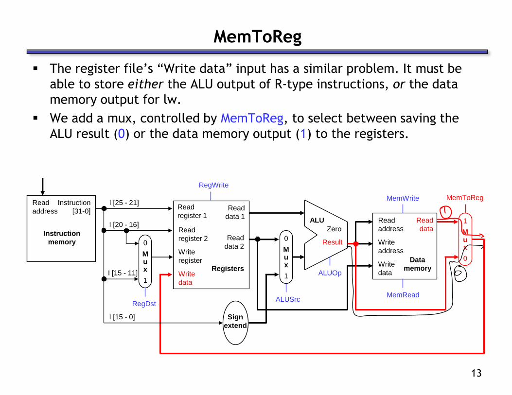
MemToReg
The register file’s ―Write data‖ input has a similar problem. It must be
able to store either the ALU output of R-type instructions, or the data
memory output for lw.
We add a mux, controlled by MemToReg, to select between saving the
ALU result (0) or the data memory output (1) to the registers.
Read
address
Write
address
Write
data
Data
memory
Read
data
MemWrite
MemRead
1
Mux
0
MemToRegRead
address
Instruction
memory
Instruction
[31-0]
I [15 - 0]
I [25 - 21]
I [20 - 16]
I [15 - 11]
0
Mux
1
RegDst
Read
register 1
Read
register 2
Write
register
Write
data
Read
data 2
Read
data 1
Registers
RegWrite
Sign
extend
0
Mux
1
ALUSrc
Result
Zero
ALU
ALUOp
14
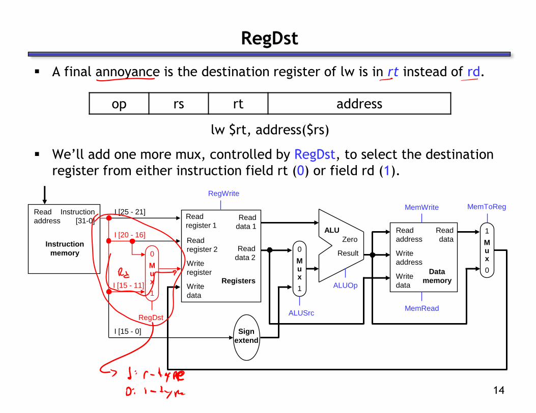
RegDst
A final annoyance is the destination register of lw is in rt instead of rd.
We’ll add one more mux, controlled by RegDst, to select the destination
register from either instruction field rt (0) or field rd (1).
op rs rt address
lw $rt, address($rs)
Read
address
Write
address
Write
data
Data
memory
Read
data
MemWrite
MemRead
1
Mux
0
MemToRegRead
address
Instruction
memory
Instruction
[31-0]
I [15 - 0]
I [25 - 21]
I [20 - 16]
I [15 - 11]
0
Mux
1
RegDst
Read
register 1
Read
register 2
Write
register
Write
data
Read
data 2
Read
data 1
Registers
RegWrite
Sign
extend
0
Mux
1
ALUSrc
Result
Zero
ALU
ALUOp

15
For branch instructions, the constant is not an address but an instruction
offset from the current program counter to the desired address.
beq $at, $0, Ladd $v1, $v0, $0add $v1, $v1, $v1j Somewhere
L: add $v1, $v0, $v0
The target address L is three instructions past the beq, so the encoding of
the branch instruction has 0000 0000 0000 0011 for the address field.
Instructions are four bytes long, so the actual memory offset is 12 bytes.
Branches
000100 00001 00000 0000 0000 0000 0011
op rs rt address

16
The steps in executing a beq
1. Fetch the instruction, like beq $at, $0, offset, from memory.
2. Read the source registers, $at and $0, from the register file.
3. Compare the values by subtracting them in the ALU.
4. If the subtraction result is 0, the source operands were equal and the PC
should be loaded with the target address, PC + 4 + (offset x 4).
5. Otherwise the branch should not be taken, and the PC should just be
incremented to PC + 4 to fetch the next instruction sequentially.

17
Branching hardware
We need a second adder, since the ALU
is already doing subtraction for the beq.
Multiply constant
by 4 to get offset.
PCSrc=1 branches
to PC+4+(offset 4).
PCSrc=0 continues
to PC+4.4
Shift
left 2
PCAdd
Add
0
Mux
1
PCSrc
Read
address
Write
address
Write
data
Data
memory
Read
data
MemWrite
MemRead
1
Mux
0
MemToRegRead
address
Instruction
memory
Instruction
[31-0]
I [15 - 0]
I [25 - 21]
I [20 - 16]
I [15 - 11]
0
Mux
1
RegDst
Read
register 1
Read
register 2
Write
register
Write
data
Read
data 2
Read
data 1
Registers
RegWrite
Sign
extend
0
Mux
1
ALUSrc
Result
Zero
ALU
ALUOp
18
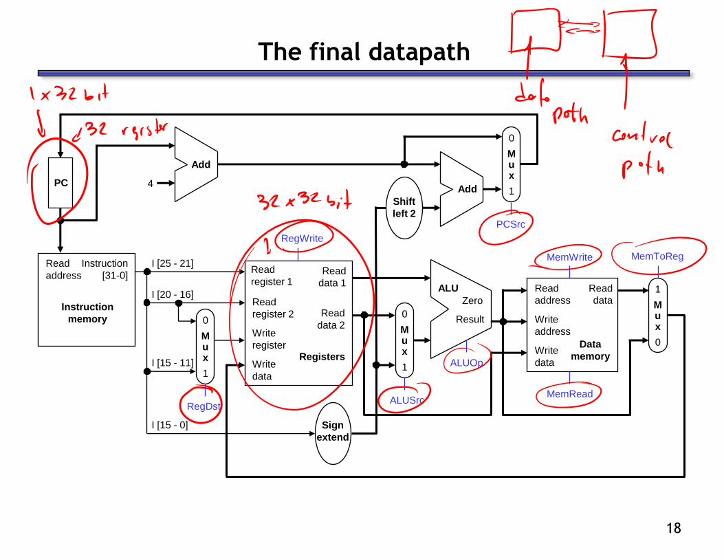
The final datapath
4
Shift
left 2
PCAdd
Add
0
Mux
1
PCSrc
Read
address
Write
address
Write
data
Data
memory
Read
data
MemWrite
MemRead
1
Mux
0
MemToRegRead
address
Instruction
memory
Instruction
[31-0]
I [15 - 0]
I [25 - 21]
I [20 - 16]
I [15 - 11]
0
Mux
1
RegDst
Read
register 1
Read
register 2
Write
register
Write
data
Read
data 2
Read
data 1
Registers
RegWrite
Sign
extend
0
Mux
1
ALUSrc
Result
Zero
ALU
ALUOp
19
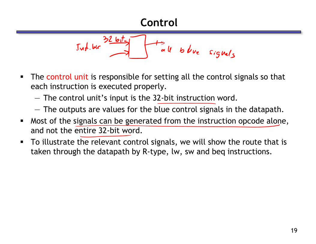
Control
The control unit is responsible for setting all the control signals so that
each instruction is executed properly.
— The control unit’s input is the 32-bit instruction word.
— The outputs are values for the blue control signals in the datapath.
Most of the signals can be generated from the instruction opcode alone,
and not the entire 32-bit word.
To illustrate the relevant control signals, we will show the route that is
taken through the datapath by R-type, lw, sw and beq instructions.
20
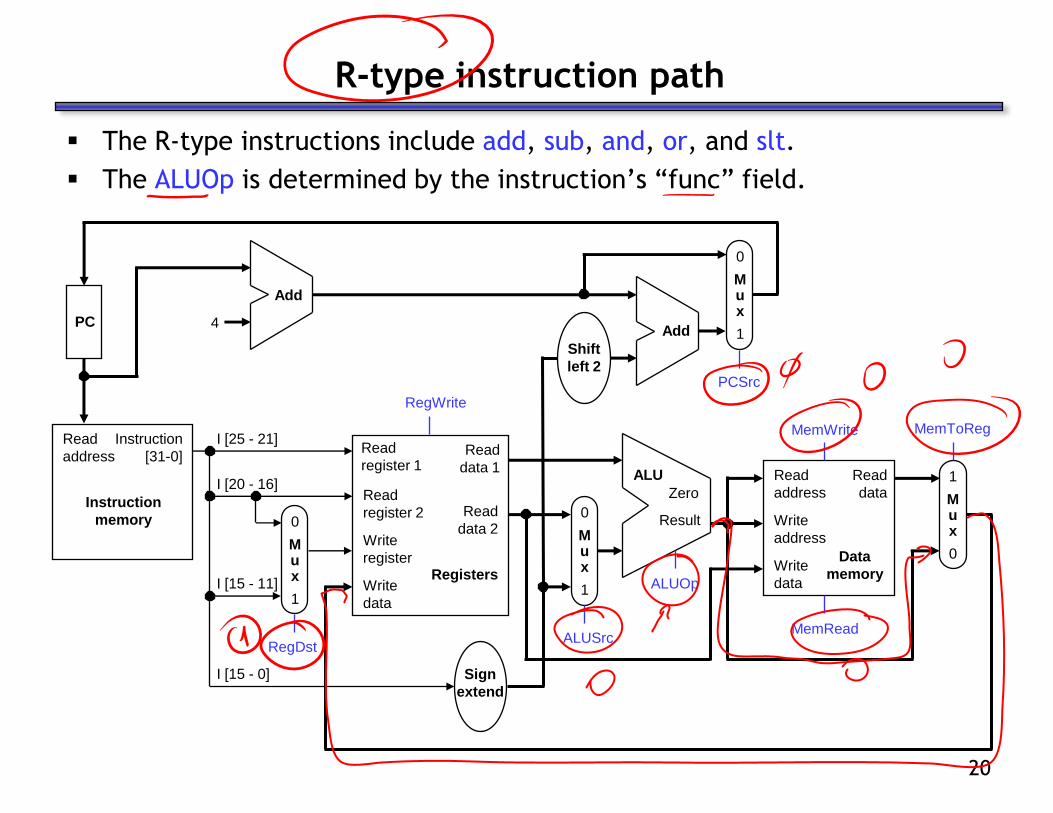
R-type instruction path
The R-type instructions include add, sub, and, or, and slt.
The ALUOp is determined by the instruction’s ―func‖ field.
4
Shift
left 2
PCAdd
Add
0
Mux
1
PCSrc
Read
address
Write
address
Write
data
Data
memory
Read
data
MemWrite
MemRead
1
Mux
0
MemToRegRead
address
Instruction
memory
Instruction
[31-0]
I [15 - 0]
I [25 - 21]
I [20 - 16]
I [15 - 11]
0
Mux
1
RegDst
Read
register 1
Read
register 2
Write
register
Write
data
Read
data 2
Read
data 1
Registers
RegWrite
Sign
extend
0
Mux
1
ALUSrc
Result
Zero
ALU
ALUOp
21
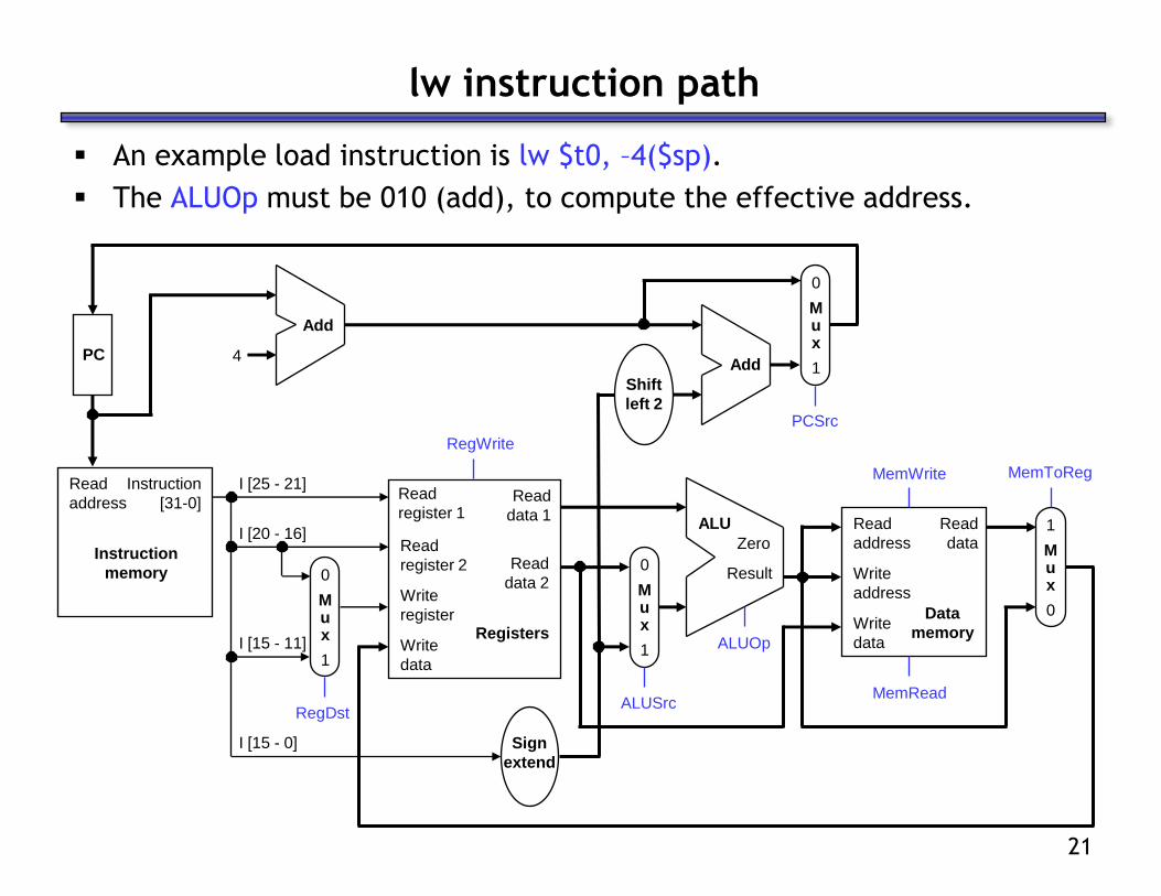
lw instruction path
An example load instruction is lw $t0, –4($sp).
The ALUOp must be 010 (add), to compute the effective address.
4
Shift
left 2
PCAdd
Add
0
Mux
1
PCSrc
Read
address
Write
address
Write
data
Data
memory
Read
data
MemWrite
MemRead
1
Mux
0
MemToRegRead
address
Instruction
memory
Instruction
[31-0]
I [15 - 0]
I [25 - 21]
I [20 - 16]
I [15 - 11]
0
Mux
1
RegDst
Read
register 1
Read
register 2
Write
register
Write
data
Read
data 2
Read
data 1
Registers
RegWrite
Sign
extend
0
Mux
1
ALUSrc
Result
Zero
ALU
ALUOp
22
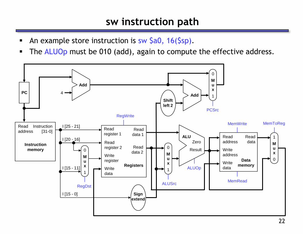
sw instruction path
An example store instruction is sw $a0, 16($sp).
The ALUOp must be 010 (add), again to compute the effective address.
4
Shift
left 2
PCAdd
Add
0
Mux
1
PCSrc
Read
address
Write
address
Write
data
Data
memory
Read
data
MemWrite
MemRead
1
Mux
0
MemToRegRead
address
Instruction
memory
Instruction
[31-0]
I [15 - 0]
I [25 - 21]
I [20 - 16]
I [15 - 11]
0
Mux
1
RegDst
Read
register 1
Read
register 2
Write
register
Write
data
Read
data 2
Read
data 1
Registers
RegWrite
Sign
extend
0
Mux
1
ALUSrc
Result
Zero
ALU
ALUOp
23
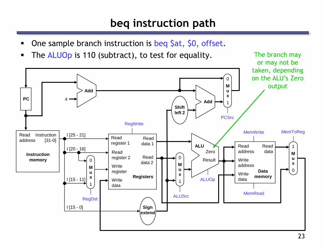
beq instruction path
One sample branch instruction is beq $at, $0, offset.
The ALUOp is 110 (subtract), to test for equality. The branch may
or may not be
taken, depending
on the ALU’s Zero
output
4
Shift
left 2
PCAdd
Add
0
Mux
1
PCSrc
Read
address
Write
address
Write
data
Data
memory
Read
data
MemWrite
MemRead
1
Mux
0
MemToRegRead
address
Instruction
memory
Instruction
[31-0]
I [15 - 0]
I [25 - 21]
I [20 - 16]
I [15 - 11]
0
Mux
1
RegDst
Read
register 1
Read
register 2
Write
register
Write
data
Read
data 2
Read
data 1
Registers
RegWrite
Sign
extend
0
Mux
1
ALUSrc
Result
Zero
ALU
ALUOp

24
Control signal table
sw and beq are the only instructions that do not write any registers.
lw and sw are the only instructions that use the constant field. They also
depend on the ALU to compute the effective memory address.
ALUOp for R-type instructions depends on the instructions’ func field.
The PCSrc control signal (not listed) should be set if the instruction is beq
and the ALU’s Zero output is true.
Operation RegDst RegWrite ALUSrc ALUOp MemWrite MemRead MemToReg
add 1 1 0 010 0 0 0
sub 1 1 0 110 0 0 0
and 1 1 0 000 0 0 0
or 1 1 0 001 0 0 0
slt 1 1 0 111 0 0 0
lw 0 1 1 010 0 1 1
sw X 0 1 010 1 0 X
beq X 0 0 110 0 0 X

25
Generating control signals
The control unit needs 13 bits of inputs.
— Six bits make up the instruction’s opcode.
— Six bits come from the instruction’s func field.
— It also needs the Zero output of the ALU.
The control unit generates 10 bits of output, corresponding to the signals
mentioned on the previous page.
You can build the actual circuit by using big K-maps, big Boolean algebra,
or big circuit design programs.
The textbook presents a slightly different control unit.
Read
address
Instruction
memory
Instruction
[31-0]
Control
I [31 - 26]
I [5 - 0]
RegWrite
ALUSrc
ALUOp
MemWrite
MemRead
MemToReg
RegDst
PCSrc
Zero
26
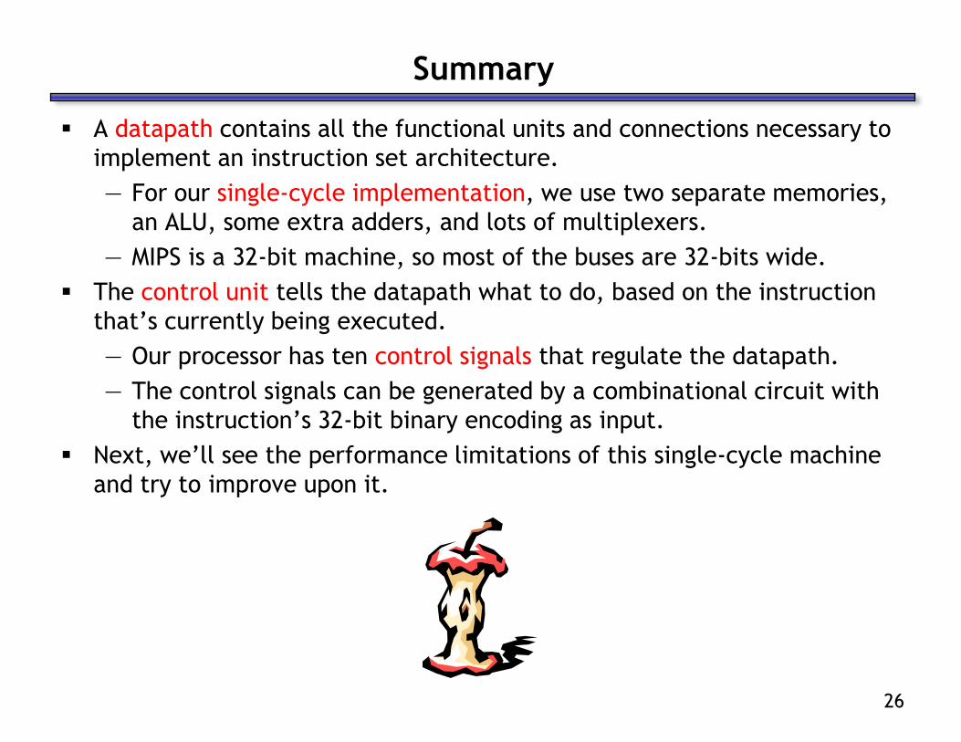
Summary
A datapath contains all the functional units and connections necessary to
implement an instruction set architecture.
— For our single-cycle implementation, we use two separate memories,
an ALU, some extra adders, and lots of multiplexers.
— MIPS is a 32-bit machine, so most of the buses are 32-bits wide.
The control unit tells the datapath what to do, based on the instruction
that’s currently being executed.
— Our processor has ten control signals that regulate the datapath.
— The control signals can be generated by a combinational circuit with
the instruction’s 32-bit binary encoding as input.
Next, we’ll see the performance limitations of this single-cycle machine
and try to improve upon it.