a role of hno3 on transparent conducting film with single...
TRANSCRIPT

A role of HNO3 on transparent conducting film with single-walled carbon nanotubes
This article has been downloaded from IOPscience. Please scroll down to see the full text article.
2009 Nanotechnology 20 475703
(http://iopscience.iop.org/0957-4484/20/47/475703)
Download details:
IP Address: 115.145.200.154
The article was downloaded on 28/10/2009 at 08:43
Please note that terms and conditions apply.
The Table of Contents and more related content is available
HOME | SEARCH | PACS & MSC | JOURNALS | ABOUT | CONTACT US

IOP PUBLISHING NANOTECHNOLOGY
Nanotechnology 20 (2009) 475703 (6pp) doi:10.1088/0957-4484/20/47/475703
A role of HNO3 on transparent conductingfilm with single-walled carbon nanotubesDong-Wook Shin1, Jong Hak Lee1, Yu-Hee Kim2, Seong Man Yu1,Seong-Yong Park3 and Ji-Beom Yoo1,2
1 SKKU Advanced Institute of Nanotechnology (SAINT), Sungkyunkwan University,300 Chunchun-dong, Jangan-gu, Suwon 440746, Republic of Korea2 Advanced Materials Science and Engineering, Sungkyunkwan University,300 Chunchun-dong, Jangan-gu, Suwon 440746, Republic of Korea3 R&D Center, Changsung Corporation, 11-9 Namdong Industrial Area, Namdong-gu,Incheon 405846, Republic of Korea
E-mail: [email protected]
Received 27 July 2009, in final form 29 September 2009Published 26 October 2009Online at stacks.iop.org/Nano/20/475703
AbstractThere is some controversy regarding the effects of HNO3 on films of single-walled carbonnanotubes (SWCNTs). In this study we examined the change in sheet resistance of anHNO3-modified SWCNT film after different drying times at 85 ◦C using various analyticaltechniques. The shift and suppression in the Raman spectra, bleaching of the transition peaksrelated to van Hove singularities and a shift in the original peak in the C 1s XPS spectraprovided evidence for p-type doping. A decrease in sheet resistance was also observed in theSWCNTs films due to the removal of residual N-methylpyrrolidone solvent on the surface andbundle of SWCNTs. These results suggest that p-type doping has a larger effect on the sheetresistance than the removal of residual N-methylpyrrolidone by an HNO3 treatment.
S Supplementary data are available from stacks.iop.org/Nano/20/475703
(Some figures in this article are in colour only in the electronic version)
1. Introduction
Single-walled carbon nanotubes have attracted considerableinterest on account of their exceptional electrical, physical andmechanical properties. In particular, transparent conductingflexible films containing single-walled carbon nanotubeswith low sheet resistance and high transmittance has beenexploited for the wide range of applications, including next-generation displays, stretchable electronic devices, opticaldevices, sensors [1] and solar cells [2]. However, furtherimprovement in the sheet resistance of SWCNT films is neededto make them an attractive alternative to indium tin oxide(ITO). The sheet resistance of transparent conducting filmswith SWCNTs is dependent on the percolation effect [3] andthe heterogeneous contact resistance of the random networks.Chemical doping and the removal of the solvent-wrappedcarbon nanotubes have been used to decrease the contactresistance between the heterogeneous junctions and enhancethe percolation effect.
There are a range of methods for doping SWCNT filmswith n-type and p-type dopants to decrease the contactresistance between the heterogeneous junctions. Chemicaldoping of SWCNT films with several alkali metals, such asLi, K and Cs, and alkaline-earth metals, such as Sr, hasresulted in n-type doping behavior [4–8]. In contrast, animprovement in the conductivity of SWCNTs films due to thespontaneous reduction of Au ions on the sidewalls of SWCNTshas been used for p-type doping [9, 10]. Similarly, I2 andBr2 intercalation of SWCNT bundles and the influence of aBrønsted acid, e.g. H2SO4, HNO3, and HCl, on the electronicproperties of SWCNTs have been used as the dopant for p-typedoping [11–13].
HNO3 can be used to remove carbon black, metal catalystsand some impurities adsorbed on the SWCNT surface duringthe purification processes. It is also used to chemicallydope SWCNTs with electron acceptors by immersing theSWCNT film in an HNO3 solution [14] and the reflux ofSWCNT powders in HNO3 [15, 16]. Recently, it wasreported that a decrease in the thickness of the SWCNT film
0957-4484/09/475703+06$30.00 © 2009 IOP Publishing Ltd Printed in the UK1

Nanotechnology 20 (2009) 475703 D-W Shin et al
through the removal of adsorbates, such as organic solventsand surfactants, can increase the conductivity of the HNO3-modified SWCNT film [17–19]. This discordant opinion aboutthe effects of HNO3 on SWCNT films has been expressedin previous papers [14–19]. (1) The improvement in theconductivity of transparent conducting films with SWCNTsdue to a decrease in the thickness of the SWCNT film throughthe removal of adsorbates was considered without the effectof chemical doping. (2) In addition, the decrease in sheetresistance with SWCNT films due to chemical doping wasconsidered without the effect of the removal of adsorbates.In the present study, the effects of the HNO3 modification ofSWCNT films were related to both chemical p-type dopingand the removal of the N-methylpyrrolidone solvent. In orderto identify the main factors for decreasing the sheet resistanceof SWCNT films immersed in HNO3, this study examined thechange in the sheet resistance of the HNO3-modified SWCNTfilm at different drying times at 85 ◦C.
2. Experiment details
The SWCNTs with a mean diameter of 1.2–1.6 nm and apurity of 90 vol%, which were synthesized by an arc dischargeprocess, were purchased from Hanwha Nanotech. In order toobtain a well-dispersed SWCNTs solution, 1 mg of an SWCNTpowder was dispersed in 100 ml of N-methylpyrrolidone(NMP, Burdick & Jackson). The mixture was sonicated in ahorn-type sonicator (VC 505, Sonics & Materials Inc.), andall sonication processes were performed in ambient conditionsfor 10 min. The SWCNT film used in this experimentwas fabricated on various substrates using a filtration-wet-transfer method [20, 21], then dried to remove the residualNMP solvent in ambient conditions at 130 ◦C for 30 min.This reference sample was compared with the SWCNT filmimmersed in HNO3 for 10 min. The HNO3-modified SWCNTfilm was dried in an oven at 85 ◦C for various times in orderto confirm the reversible reaction between the HNO3/NO2
molecules and bundles of SWCNTs.UV–vis–NIR absorption spectroscopy (Shimadzu UV-
3600) was used to characterize the change in intensity inthe van Hove singularity-related transition peaks, ES
11, ES22
and EM11 through the doping or de-doping of SWCNT films.
Raman spectroscopy (Kaiser Optical System Model RXN 1)was also used to characterize the optical properties of thedoped or de-doped SWCNTs. Several excitation energiesof 1.96 eV (632.8 nm, helium–neon gas laser) and 1.58 eV(785 nm, invictus NIR diode laser) were used. The SWCNTfilm used for the Raman measurement was fabricated on SiO2
using a filtration-wet-transfer (FWT) method and the datawas collected on numerous spots (five spots) on the sample.All Raman spectra were normalized to the intensity of theG-band to allow a visual comparison between the samples.X-ray photoelectron spectroscopy (XPS) of the as-preparedSWCNT film and HNO3-modified SWCNT film indicatedthe doping agent and removal of the residual NMP solvent.The change in the thickness and sheet resistance of the as-prepared SWCNT film and HNO3-modified SWCNT film were
measured by atomic force microscopy (AFM, Veeco, 840-012-711) and a four-point probe resist meter (AIT CMT-SR1000N), respectively.
3. Results and discussion
The transparent conducting films (TCFs) with SWC-NTs were fabricated using a filtration-wet-transfer (FWT)method [20, 21]. In order to transfer the SWCNT filmfrom the filter to a polyethylene terephthalate (PET) substrate,conformal contact was first made between the filter and PET.Lateral transfer of the SWCNT film occurred as a result ofwater flowing through the filter channels in the deionized waterbath. After complete wetting, the filter was separated fromthe set and an SWCNT film was formed on the PET substrate.The film thickness could be controlled simply by varying thefiltration volume of the suspensions. Homogeneous SWCNTfilms on the PET substrate could be made in just a few secondswithout any chemical treatments. The SWCNT solution usedin the experiments was obtained by dispersing an SWCNTpowder in an NMP solvent. Monodisperse SWCNTs in theNMP solvent have been reported [22]. The mixed solutionof the SWCNTs and the NMP solvent was sonicated withoutcentrifugation to obtain a well-dispersed SWCNT solution.After immersion in HNO3 for 10 min, TCF with SWCNTsfabricated using a well-dispersed SWCNT solution had a sheetresistance of ∼100 �/sq and 48.5 �/sq at a transmittance of90% and 83%, respectively (see supporting information figureS1 available at stacks.iop.org/Nano/20/475703).
In order to identify the main factor for the decrease insheet resistance of the SWCNT film immersed in HNO3,this study examined the change in sheet resistance of theHNO3-modified SWCNT film with drying time at 85 ◦C.Figure 1 shows a sheet resistance of the as-prepared SWCNTfilm, HNO3-treated SWCNT film and a dried sample as afunction of the transmittance. The sheet resistance of theSWCNT film decreased by a factor of 10–12 (solid circleline) after immersing the as-prepared SWCNTs film in HNO3
for 10 min, whereas the changes in transmittance at 550 nmwere negligible. The sheet resistance of the HNO3-modifiedSWCNT film increased with increasing drying time from10 min to 89 h at 85 ◦C but there was no further increasein the sheet resistance of TCF with SWCNTs dried for 89 hor above. In the case of 89 h, the sheet resistance of thedried SWCNT film was lower than that of the as-preparedSWCNT film (a double-headed arrow, (1)). This suggests thata decrease in the sheet resistance of a dried SWCNT film wasdue to the enhancement of contact between tubes because ofthe removal of residual NMP on the tube–tube junction andthe surface of SWCNT networks (see supporting informationfigure S2 available at stacks.iop.org/Nano/20/475703). Theinset in figure 1 shows that the sheet resistance of the SWCNTfilm dried for 120 min was double that of the HNO3-modifiedSWCNT film. The lack of a further increase in the sheetresistance of the SWCNT film dried for 89 h suggests that theHNO3-modified SWCNT film had been completely de-doped(a double-headed arrow, (2)). This indicates that the increasein sheet resistance was due to the removal of dopants, such
2

Nanotechnology 20 (2009) 475703 D-W Shin et al
Figure 1. Transmittance versus sheet resistance for transparentconducting film generated from as-prepared, HNO3-modified anddried SWCNTs at 550 nm wavelength. A double-headed arrow (1)and (2) is related to removal of NMP and p-doping, respectively.Inset shows the change in sheet resistance of HNO3-modifiedSWCNTs at different drying times at 85 ◦C.
as HNO3/NO2 molecules physisorbed on the surface and thebundle of the SWCNTs. This study suggests that a decreasein the sheet resistance of the HNO3-modified SWCNT filmis related to both chemical doping and removal of the NMPsolvent.
Figure 2 shows the UV–vis–NIR absorption spectra ofthe as-prepared SWCNT film, doped SWCNT film afterimmersion in HNO3 for 10 min and de-doped SWCNT filmafter drying at 85 ◦C for different times. The van Hovesingularities-related transition peaks correspond to the intrinsicexcitonic transitions of semiconducting (ES
11, ES22 and ES
33)and metallic (EM
11 and EM22) SWNTs from the valence band
to the conduction band can be observed in these absorptionspectra. These peaks were fully bleached after the HNO3
treatment for 10 min. Interestingly, a new peak appearedat approximately 1.09 eV. Kim et al examined SWCNTsdoped with various concentrations of AuCl3 and reported thatthe van Hove singularity transitions disappeared graduallyin the UV–vis–NIR absorption spectra with increasing p-doping concentration and the work function of the SWCNTsincreased [9]. In particular, the disappearance of the vanHove singularities, such as the ES
11, ES22 and EM
11 bands, inthe spectra of HNO3-modified SWCNT films suggest that theFermi level was shifted further down below the second and firstvan Hove singularity in the valence band of the semiconductorand metallic nanotube, respectively. A new transition peak nearES
22 might appear because a newly empty valence band canoccur from a deeper energy level in the valence band. However,a further study will be needed to analyze the new transition.After drying for 5 min at 85 ◦C, the ES
22 peak intensity wasrestored primarily at the higher energy side, and the ES
22 peak
Figure 2. UV–vis–NIR optical absorption spectra with increasingdrying time after immersion in HNO3 for 10 min. The star indicatethe appearance of van Hove singularity transitions of p-dopedSWCNTs and the new peak induced at HNO3-modified SWCNTs.ES
ii and EMii indicate the van Hove singularity transitions between the
i th energy levels of the semiconducting and metallic SWCNT.
began to be shifted toward a lower energy side and the intensityof the ES
22 peak increased with increasing drying time. The ES11
peak and EM11 peak intensities were restored after drying for
10 min and 1 min, respectively. Similarly, the intensity of thetwo van Hove singularities-related transition peaks, ES
11 andEM
11, have also begun to increase with increasing drying timeuntil the intensity was restored completely. This indicates thatthe dopant physisorbed on the surface and bundles of SWCNTswas readily detached and the Fermi level located below thesecond and first van Hove singularity of the semiconductor andmetallic nanotube in the valence band was shifted graduallytoward the first van Hove singularity position or above withincreasing drying time, resulting in an increase in the sheetresistance of the SWCNT film.
The strong and non-monotonic dependence of theSWCNT Raman spectra on the laser excitation energy Elaser
demonstrated Raman scattering associated with a resonanceprocess for the excitation laser energy Elaser with the opticaltransition energy Eii between the van Hove singularities inthe valence band and the conduction band [23]. Ramanspectroscopy (figure 3) provided further evidence for thechemical modification of the SWCNTs with electron acceptors.At an excitation energy of 1.96 eV, the metallic andsemiconducting SWCNTs were excited in the as-preparedSWCNT film, as shown in figure 3(a). In particular, theRaman spectra of the as-prepared SWCNTs film exhibitedasymmetry on the lower Raman shift of the G-band atapprox. 1550 cm−1 (G−). This asymmetry was attributed tothe metallic SWCNTs, which is known as a Breit–Wigner–Fano (BWF) lineshape originating from an interaction of
3

Nanotechnology 20 (2009) 475703 D-W Shin et al
Figure 3. Raman spectra of as-prepared, HNO3-modified and dried SWCNT films at an excitation energy of (a) 1.96 eV and (b) 1.58 eV. Insetof (a) and (b) shows blueshift and redshift in the G band. All Raman spectra were normalized by the G-band intensity. The arrow shows thedecrease and increase of G′-band intensity after immersion in HNO3 and drying, respectively.
the phonons with continuum electronic excitations [24]. Adecrease in the BWF line was observed in the Raman spectra ofHNO3-modified SWCNT films. It was previously reported thatthe suppression of BWF in the Raman spectra of the SOCl2-treated SWCNTs was attributed to the loss of continuum statesdue to chemical modification [25]. Similarly, in the HNO3
treatment, the suppression of BWF was also assigned to theloss of continuum states. However, Geng et al reported thatthe development of the Fano line at the lower energy sideof the G band due to the HNO3 treatment is evidence of theenhancement of the metallicity in a film, and the enhancementof metallicity clearly reduced the resistance of the SWCNTsthemselves [17]. It should be noted that a decrease in theresistance of the SWCNTs is irrelevant to the enhancementof metallicity because the data showed a decrease in sheetresistance with SWCNT films notwithstanding the suppressionof BWF. A blueshift of 14.1 cm−1 (inset in figure 3(a)) anda downward shift of 9.9 cm−1 (downward arrow in the rightside of figure 3(a)) was observed in the G band and G′ band,respectively, due to the transfer of the electrons from theSWCNTs to the dopants. This phenomenon occurred in the Gband of the heavily doped p-type SWCNTs by intercalating I2
and Br2 [26], and a SOCl2 [25] treatment. In addition Corioet al [27] used the blueshift in the G′ band as a gauge of
charge transfer when SWCNTs were treated electrochemicallywith H2SO4. As the drying time was increased from 10 to120 min at 85 ◦C, the position of the G band and G′ band of theHNO3-modified SWCNT film showed a gradual redshift (insetin figure 3(a)) and an upward shift (upward arrow in the rightside of figure 3(a)) due to a gradual decrease in electron transferfrom the SWCNTs to the dopants by the HNO3 treatment. Thiswas related to the detachment of the dopants. The non-covalentinteraction between the SWCNTs and dopants was attributed tothe negligible change in the intensity of the D band. Similarly,for the 1.58 eV Elaser, a blue shift of 4.8 cm−1 (inset infigure 3(b)) and a downward shift of 21.6 cm−1 (downwardarrow on the right side of figure 3(b)) in the G band and G′band, respectively, was observed in the Raman spectra of theHNO3-treated SWCNT film. As drying time was increasedfrom 10 to 120 min, the shift in the G band and G′ band ofthe HNO3-modified SWCNT film showed a gradual redshift(inset in figure 3(b)) and an upward shift (upward arrow on theright side of figure 3(b)).
Dopants and the removal of the NMP solvent wereobserved from the XPS spectra of SWCNT films treated withHNO3 for 10 min. The inset in figure 4(a) shows that thepeak position in C 1s of the HNO3-treated SWCNT film was
4
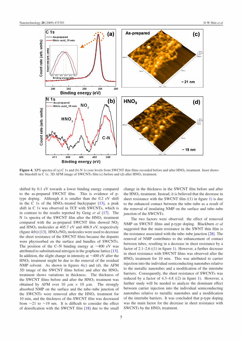
Nanotechnology 20 (2009) 475703 D-W Shin et al
Figure 4. XPS spectra of (a) C 1s and (b) N 1s core levels from SWCNT thin films recorded before and after HNO3 treatment. Inset showsthe blueshift in C 1s. 3D AFM image of SWCNTs film (c) before and (d) after HNO3 treatment.
shifted by 0.1 eV towards a lower binding energy comparedto the as-prepared SWCNT film. This is evidence of p-type doping. Although it is smaller than the 0.2 eV shiftin the C 1s of the HNO3-treated buckypaper [13], a peakshift in C 1s was observed in TCF with SWCNTs, which isin contrast to the results reported by Geng et al [17]. TheN 1s spectra of the SWCNT film after the HNO3 treatmentcompared with the as-prepared SWCNT film showed NO2
and HNO3 molecules at 405.7 eV and 406.9 eV, respectively(figure 4(b)) [13]. HNO3/NO2 molecules were used to decreasethe sheet resistance of the SWCNT films because the dopantswere physisorbed on the surface and bundles of SWCNTs.The position of the C–N binding energy at ∼400 eV wasattributed to substitutional nitrogen in the graphene lattice [13].In addition, the slight change in intensity at ∼400 eV after theHNO3 treatment might be due to the removal of the residualNMP solvent. As shown in figures 4(c) and (d), the AFM3D image of the SWCNT films before and after the HNO3
treatment shows variations in thickness. The thickness ofthe SWCNT films before and after the HNO3 treatment wasobtained by AFM over 10 μm × 10 μm. The stronglyabsorbed NMP on the surface and the tube–tube junction ofthe SWCNTs were removed after the HNO3 treatment for10 min, and the thickness of the SWCNT film was decreasedfrom ∼21 to ∼19 nm. It is difficult to consider the effectof densification with the SWCNT film [18] due to the small
change in the thickness in the SWCNT film before and afterthe HNO3 treatment. Instead, it is believed that the decrease insheet resistance with the SWCNT film ((1) in figure 1) is dueto the enhanced contact between the tube–tube as a result ofthe removal of insulating NMP on the surface and tube–tubejunction of the SWCNTs.
The two factors were observed: the effect of removedNMP on SWCNT films and p-type doping. Blackburn et alsuggested that the main resistance in the SWNT thin film isthe resistance associated with the tube–tube junction [28]. Theremoval of NMP contributes to the enhancement of contactbetween tubes, resulting in a decrease in sheet resistance by afactor of 2.1–2.6 ((1) in figure 1). However, a further decreasein sheet resistance with SWCNT films was observed after theHNO3 treatment for 10 min. This was attributed to carrierinjection into the individual semiconducting nanotubes relativeto the metallic nanotubes and a modification of the intertubebarriers. Consequently, the sheet resistance of SWCNTs wasreduced by a factor of 4.3–4.8 ((2) in figure 1). However, afurther study will be needed to analyze the dominant effectbetween carrier injection into the individual semiconductingnanotubes relative to metallic nanotubes and a modificationof the intertube barriers. It was concluded that p-type dopingwas the main factor for the decrease in sheet resistance withSWCNTs by the HNO3 treatment.
5

Nanotechnology 20 (2009) 475703 D-W Shin et al
4. Conclusions
Transparent conducting films containing SWCNTs werefabricated on various substrates using the filtration-wet-transfer method. The sheet resistance and correspondingtransmittance of the transparent conducting film with SWCNTsafter immersion in HNO3 for 10 min ranged from ∼100 �/sqto 48.5 �/sq and from 90% to 83%, respectively. TheHNO3-treated SWCNT film chemically doped with an electronacceptor showed bleaching of the van Hove singularity in theUV–vis–NIR absorption spectra, a blueshift and a downwardshift in the G band and G′ band, respectively, a decrease in theBWF line in the Raman spectra and a blueshift of 0.1 eV inthe C 1s peak in the XPS spectra. After thermal treatment at85 ◦C, the Fermi level located below the second and first vanHove singularity of the semiconducting and metallic nanotubesin the valence band was shifted toward the original position onthe electronic structure with the as-prepared SWCNTs. Theenhanced contact between tubes due to the removal of the NMPsolvent was attributed to a decrease in the sheet resistance ofthe SWCNT film dried for 89 h compared to the as-preparedSWCNT film. These results suggest that p-type doping is themain factor for the decrease in the sheet resistance of the filmscontaining SWCNTs by the HNO3 treatment.
Acknowledgments
This study was funded by the BK21 Project of ChangsungCorporation and Seoul Fellowship to J H Lee.
References
[1] Cattanach K, Kulkarni R D, Kozlov M and Manohar S K 2006Nanotechnology 17 4123–8
[2] Contreras M A, Barnes T, Lagemaat J, Rumbles G, Coutts T J,Weeks C, Glatkowski P, Levitsky I, Peltola J and Britz D A2007 J. Phys. Chem. Lett. C 111 14045–8
[3] Hu L, Hecht D S and Gruner G 2004 Nano Lett. 4 2513–7[4] Lee R S, Kim H J, Fischer J E, Thess A and Smalley R E 1997
Nature 388 255–7
[5] Grigorian L, Sumanasekera G U, Loper A L, Fang S, Allen J Land Eklund P C 1998 Phys. Rev. B 58 R4195–8
[6] Kong J, Zhou C, Yenilmez E and Dai H 2000 Appl. Phys. Lett.77 3977–9
[7] Chen B, Li B and Chen L 2008 Appl. Phys. Lett. 93 043104[8] Kim B H, Park T H, Baek T H, Lee D S, Park S J, Kim J S and
Park Y W 2008 J. Appl. Phys. 103 096103[9] Kim K K et al 2008 J. Am. Chem. Soc. 130 12757–61
[10] Kong B-S, Jung D-H, Oh S-K, Han C-S and Jung H-T 2007J. Phys. Chem. C 111 8377–82
[11] Sankapal B R, Setyowati K and Chen J 2007 Appl. Phys. Lett.91 173103
[12] Nascimento G M, Hou T, Kim Y A, Muramatsu H, Hayashi T,Endo M, Akuzawa N and Dresselhaus M S 2008 Nano Lett.8 4168–72
[13] Graupner R, Abraham J, Vencelova A, Seyller T, Hennrich F,Kappes M M, Hirsch A and Ley L 2003 Phys. Chem. Chem.Phys. 5 5472–6
[14] Jackson R, Domercq B, Jain R, Kippelen B and Graham S 2008Adv. Funct. Mater. 18 2548–54
[15] Hennrich F, Wllmann R, Malik S, Lebedkin S and Kappes M M2003 Phys. Chem. Chem. Phys. 5 178–83
[16] Wu M-C, Lin Y-Y, Chen S, Liao H-C, Wu Y-J, Chen C-W,Chen Y-F and Su W-F 2009 Chem. Phys. Lett. 468 64–8
[17] Geng H Z, Kim K K, So K P, Lee Y S, Chang Y and Lee Y H2007 J. Am. Chem. Soc. 129 7758–9
[18] Geng H-Z, Lee D S, Kim K K, Han G H, Park H K and Lee Y H2008 Chem. Phys. Lett. 455 275–8
[19] Geng H-Z et al 2008 J. Mater. Chem. 18 1261–6[20] Shin J-H, Shin D W, Patole S P, Lee J H, Park S M and Yoo J B
2009 J. Phys. D: Appl. Phys. 42 045305[21] Lee J H, Shin D W, Makotchenko V G, Nazarov A S,
Fedorov V E, Kim Y H, Choi J-Y, Kim J M and Yoo J B2009 Adv. Mater. 21 doi:10.1002/adma.200900726
[22] Bergin S D et al 2008 Adv. Mater. 20 1876–81[23] Rao A M, Richter E, Bandow S, Chase B and Eklund P C 1997
Science 275 187–91[24] Brown S D M, Jorio A, Corio P, Dresselhaus M S,
Dresselhaus G, Saito R and Kneipp K 2001 Phys. Rev. B63 155414
[25] Weglikowska U D et al 2005 J. Am. Chem. Soc. 127 5125–31[26] Rao A M, Bandow S, Richter E and Eklund P C 1998 Thin
Solid Films 331 141–7[27] Corio P, Santos P S, Brar V W, Samsonidze G G, Chou S G
and Dresselhaus M S 2003 Chem. Phys. Lett. 370 675–82[28] Blackburn J L, Barnes T M, Beard M C, Kim Y H, Tenent R C,
McDonald T J, To B, Coutts T J and Heben M J 2008 ACSNano 2 1266–74
6