a-pdf split demo : purchase from to remove ... · on is 2-3 v in a 1000v device). similar to the...
TRANSCRIPT

100 ECN-C--00-019
loss standpoint, 300-400-Y MOSFETs compete with bipolar transistors only if the switchingfrequency is in excess of 30-100 kHz. However, no definite statement can he made about thecrossover frequency because it depends on the operating voltages, with low voltages favouringthe MOSFET.
MOSFETs are available in voltage ratings in excess of 1000 V but with small current ratingsand with up to 100 A at small voltage ratings. The maximum gate-source voltage is ±20 V,although MOSFETs are available, which can be controlled by 5V signals. Because their on-state resistance has a positive temperature coefficient, MOSFETs are easily paralleled. Thiscauses the device conducting the higher current to heat up and thus forces it to share its currentequally with the other MOSFETs in parallel.
INSULATED GATE BIPOLAR TRANSISTORS (IGBT)
The circuit symbol for an IGBT is shown in Fig. 5.16a and its i-v characteristics are shown inFig. 5.16b. The IGBTs have some of the advantages of the MOSFET, the BJT, and the GTOcombined. Similar to the MOSFET, the IGBT has a high impedance gate, which requires only asmall amount of energy to switch the device. Like the BJT, the IGBT has a small on-statevoltage even in devices with large blocking voltage ratings (for example, Von is 2-3 V in a1000V device). Similar to the GTO, IGBTs can be designed to block negative voltages, as theiridealised switch characteristics shown in Fig. 5.16c indicate.
Fig. 5.16 IGBT characteristics
Insulated gate bipolar transistors have turn-on and turn-off times of the order of 1 µs and areavailable in module ratings as large as 1700 V and 1200 A. Voltage ratings of up to 2- 3 kV areprojected.
5.8.2 Gate and base drive circuits
A-PDF Split DEMO : Purchase from www.A-PDF.com to remove the watermark

ECN-C--00-019 101
PRELIMINARY DESIGN CONSIDERATIONS
The primary function of a drive circuit is to switch a power semiconductor device from the offstate to the on state and vice versa. In most situations the designer seeks a low cost drive circuitthat minimises the turn-on and turn-off times so that the power device spends little time intraversing the active region where the instantaneous power dissipation is large. In the on statethe drive circuit must provide adequate drive power (e.g., base current to a BJT or gate-sourcevoltage to a MOSFET) to keep the power switch in the on state where the conduction losses arelow. Very often the drive circuit must provide reverse bias to the power switch control terminalsto minimise turn-off times and to ensure that the device remains in the off-state and is nottriggered on by stray transient signals generated by the switching of other power devices.
The signal processing and control circuits that generate the logic-level control signals used toturn the power switch on and off are not considered part of the drive circuit. The drive circuit isthe interface between the control circuit and the power switch. The drive circuit amplifies thecontrol signals to levels required to drive the power switch and provides electrical isolationwhen required between the power switch and the logic-level signal processing control circuits. Often the drive circuit has significant power capabilities compared to the logic-level controlsignal processing circuits. For example, power BJTs have low values of beta, typically 5 - 10, sothat the base current supplied by the drive circuit is often a significant fraction of the total loadcurrent.
The basic topology of the drive circuit is dictated by three functional considerations. Firstly, isthe output signal, provided by the drive circuit, unipolar or bipolar? Unipolar signals lead tosimpler drive circuits, but bipolar signals are needed for rapid turn-on and turn-off of the powerswitch. Secondly, can the drive signals be directly coupled to the power switch, or is electricalisolation required between the logic-level control circuits and the power device? Mostelectrically isolated drive circuits will require isolated de power supplies. Thirdly, is the outputof the drive circuit connected in parallel with the power switch (the usual situation) or in serieswith the switch (cascode connection)?
Additional functionality may be required of the drive circuit, which will further influence thetopological details of the circuit. Provisions may be included in the drive circuit design forprotection of the power switch from overcurrents. Then communication between the drivecircuit and the control circuit is needed. In bridge circuits, the drive circuit must often provideblanking times for the power switch. Incorporation of these types of functionality requiresdesign inputs to both the drive circuit and the logic-level control circuit. Waveshaping of thedrive circuit output may also he included to improve the power switch performance.
The specific details of component values to be used in a drive circuit will vary depending on thecharacteristics of the power switch being driven. For example, MOSFET drive circuits needonly provide an initial large current as the device turns on and for the rest of the on-state timeinterval merely provide a large gate-source voltage at low current levels.
It is a good idea to consider how the drive circuit will be configured on a circuit board even atthe earliest stages in the design process. The placement of components to minimise strayinductance and to minimise susceptibility to switching noise may affect the choice of topologyfor the drive circuit.
DC-coupled drive circuits
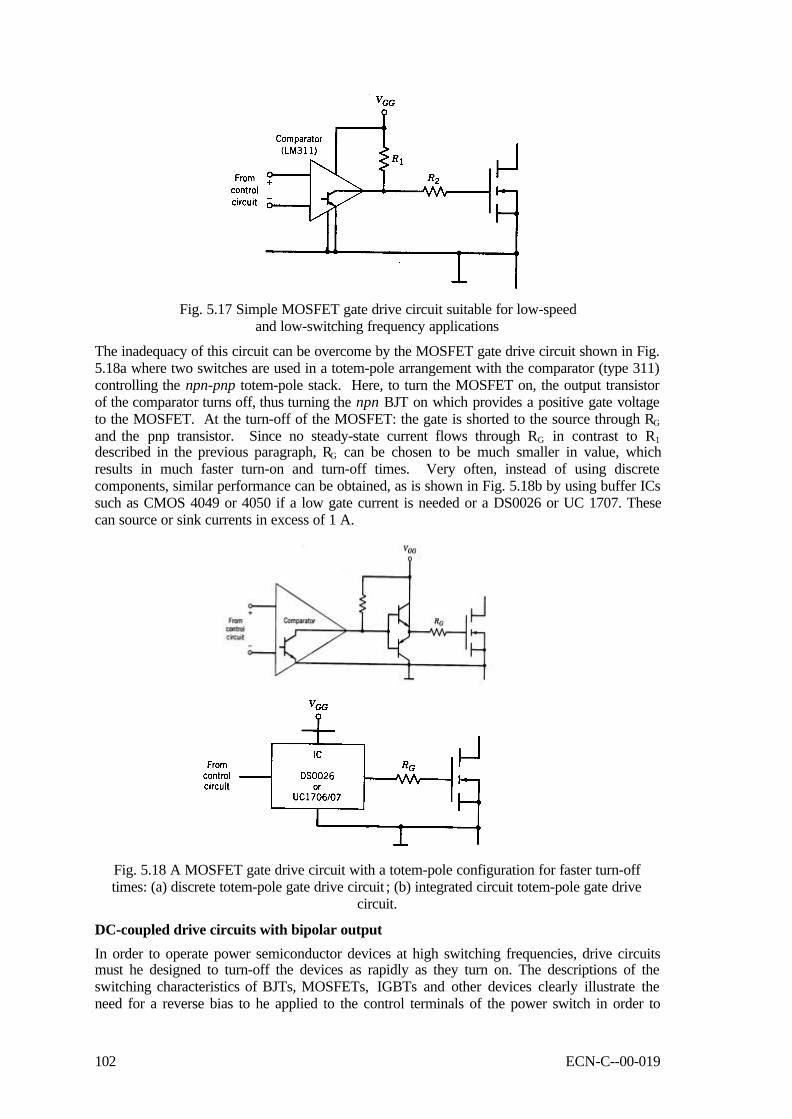
A simple MOSFET gate drive circuit with only one switch to control the gate current is shownin Fig. 5.17, where the output transistor of a comparator (e.g. LM31 1) controls the MOSFET. When the output transistor is off, the MOSFET is on and vice versa. When the comparator ison, it must sink a current VGG/IR1, and to avoid large losses in the drive circuit, RI should belarge. This will slow down the MOSFET turn-on time. This means that the drive circuit is onlysuitable for low switching speed applications.
102 ECN-C--00-019
Fig. 5.17 Simple MOSFET gate drive circuit suitable for low-speedand low-switching frequency applications
The inadequacy of this circuit can be overcome by the MOSFET gate drive circuit shown in Fig.5.18a where two switches are used in a totem-pole arrangement with the comparator (type 311)controlling the npn-pnp totem-pole stack. Here, to turn the MOSFET on, the output transistorof the comparator turns off, thus turning the npn BJT on which provides a positive gate voltageto the MOSFET. At the turn-off of the MOSFET: the gate is shorted to the source through RG
and the pnp transistor. Since no steady-state current flows through RG in contrast to R1
described in the previous paragraph, RG can be chosen to be much smaller in value, whichresults in much faster turn-on and turn-off times. Very often, instead of using discretecomponents, similar performance can be obtained, as is shown in Fig. 5.18b by using buffer ICssuch as CMOS 4049 or 4050 if a low gate current is needed or a DS0026 or UC 1707. Thesecan source or sink currents in excess of 1 A.
Fig. 5.18 A MOSFET gate drive circuit with a totem-pole configuration for faster turn-offtimes: (a) discrete totem-pole gate drive circuit ; (b) integrated circuit totem-pole gate drive
circuit.
DC-coupled drive circuits with bipolar output
In order to operate power semiconductor devices at high switching frequencies, drive circuitsmust he designed to turn-off the devices as rapidly as they turn on. The descriptions of theswitching characteristics of BJTs, MOSFETs, IGBTs and other devices clearly illustrate theneed for a reverse bias to he applied to the control terminals of the power switch in order to

ECN-C--00-019 103
affect a rapid turn-off. Drive circuits with unipolar outputs are unable to provide the reversebias required and are thus incapable of providing fast turn-off of power devices. In order toprovide a reverse bias to the control terminals of the power device, the drive circuit must have abipolar output (an output that can be either positive or negative). This in turn requires that thedrive circuit is biased by a negative power supply as well as a positive power supply.
Fig. 5.19 Various gate-drive circuits using split DC power supplies for providing an n-channelMOSFET with positive gate-source voltages at turn-on and negative gate-drive at turn-off
A drive circuit for MOSFETs that provides positive gate voltages at turn on and negative gatevoltages at turn off by means of a split power supply with respect to the MOSFET source isshown in Figs. 5.19a to 5.19c. If the control signal is supplied by the logic circuit, which isconnected between VGG, and the source of the MOSFET, then the reference input to thecomparator should he shifted to be at the mid-potential between VGG, and the MOSFET sourceusing a pre-converter circuit.
ELECTRICALLY ISOLATED DRIVE CIRCUITS
Very often, there is a need for electrical isolation between the logic-level control signals and thedrive circuits. The basic ways to provide electrical isolation are either by optocouplers, fiberoptics or by transformers.
OPTOCOUPLER ISOLATED DRIVE CIRCUITS
The optocoupler consists of a light-emitting diode (LED), the output transistor, and a built-inSchmitt trigger. A positive signal from the control logic causes the LED to emit light that isfocused on the optically sensitive base region of a phototransistor. In optocoupler-isolated drivecircuits, the optocoupler itself is the interface between the output of the control circuit and theinput of the isolated drive circuit. The input side of the optocoupler is directly coupled to thecontrol circuit and the output side of the optocoupler is directly connected to the isolated drivecircuit. The topology of the isolated drive circuit between the output of the optocoupler and thecontrol terminal of the power switch can take many different forms.
Optocoupler-isolated drive circuits can also be used with power MOSFETs and IGBTs. Thecircuit shown in Fig. 5.20 uses a high common-anode noise immunity optocoupler (HPCL-4503) and a high-speed driver (IXLD4425) with a 3A output capability. The drive circuit uses asingle-ended floating IS-V supply and provides a ±15V output voltage for high noise immunity

104 ECN-C--00-019
and fast switching to drive the gate of a power MOSFET or IGBT. The integrated high-speeddriver circuit connects the gate of the power device to the 15-V bus bar while it simultaneouslyconnects the source to the negative side of the bias supply in order to turn the power device on. To turn the power device off, the drive circuit connects the gate to the negative side of thesingle-ended supply while it connects the source to the +15-V bus bar.
Fig. 5.20 Optocoupler isolation of base drive circuits
TRANSFORMER-ISOLATED DRIVE CIRCUITS PROVIDING BOTH SIGNAL ANDPOWER
The use of transformers for electrically isolating the drive circuit from the control circuitintroduces a great deal of flexibility into the design of the drive circuit. The same transformerused to transfer the control signal from the control circuits to the isolated drive circuit can alsobe used to provide the isolated bias power and to replace a separate transformer for the isolatedsupplies.
Fig. 5.21 Transformer-isolated MOSFET gate drive circuit using a high-frequency carriers sothat the MOSFET can be held on for long periods. No auxiliary DC power supplies are needed
since both the control signal and bias power come through the transformer.
If in a given application, the MOSFET to be controlled is to be on for a long time, the circuitshown in Fig. 5.21 can be used. In this circuit a high-frequency oscillator output modulates thecontrol voltage before being applied to the buffer circuits. Now a high-frequency ac signal

ECN-C--00-019 105
appears across the transformer primary when the control voltage is high. Thus charging theenergy storage capacitance C1 and the capacitance C2 at the input to the 7555 IC, which is usedhere as a buffer and a Schmitt trigger because of its low power consumption. With the input tothe 7555 low, it provides a positive voltage to the MOSFET gate, thus turning it on as is shownin Fig. 5.21. At turn off, the control voltage goes low and the voltage across the transformerprimary goes to zero. Now C2 discharges through R2 and the input voltage to the 7555 goeshigh, which causes its output voltage to go low, thus turning the MOSFET off. The diode DB isused to prevent the energy stored in the capacitance C1 from discharging into the resistance R2.
POWER DEVICE PROTECTION IN DRIVE CIRCUITS
OVERCURRENT PROTECTION
In some applications the potential may exist for currents to flow through a power device thatexceed the capability of the device. If the device is not somehow protected against theseovercurrents, it may be destroyed. Power devices cannot be protected against the overcurrentsby fuses because they can not act fast enough. Overcurrents can be detected by measuring thedevice current and comparing it against a limit. At currents above this limit, a protectionnetwork in the drive circuit turns off the power device.
A cheaper and normally better way of providing overcurrent protection is to monitor theinstantaneous output voltage of the device, for example, the collector-emitter on-state voltage ofa BJT or the drain-source voltage of a MOSFET. Fig. 5.22a shows a simple circuit to provideovercurrent protection to a BJT based on this principle. The voltage during the on state at pointC will be one forward-bias diode drop above VCEsat. This voltage signal is one of the inputs tothe overcurrent protection block that requires the control signal as another input. When thetransistor is supposed to be on, if the voltage at point C with some delay is above somepredetermined threshold, the overcurrent is detected, and the protection block causes the basedrive to turn the BJT off. Depending on the design philosophy, the overall system may be shutdown after such an overcurrent detection and may have to be manually reset. The overcurrentdetection network can be combined with the anti-saturation network as is shown in the sub-circuit of Fig. 5.22b.

106 ECN-C--00-019
Fig 5.22 (a) overcurrent protection by measuring the instantaneous on-state collector-emittervoltage of the power transistors (b) this protection circuit can be used with an anti-saturation
network.
The overcurrent protection should he combined with design measures that limit the maximuminstantaneous current through the device. The overcurrent protection circuit must act within afew microseconds to turn off the MOSFET, otherwise it will be destroyed.
BLANKING TIMES FOR BRIDGE CIRCUITS
In the half-bridge and full-bridge circuits, where two transistors are connected in series in oneconverter leg, it is important to provide a blanking time. In this way the turn-on control input toone transistor is delayed with respect to the turn-off control input of the other transistor in theinverter leg. This blanking time should be chosen conservatively to be greater than the worst-case maximum storage time of the transistors being used to avoid cross conduction. Undernormal operation, such a conservatively chosen blanking time will cause a dead time equal tothe blanking time minus the actual delay time to occur in which both the transistors in theinverter leg are off. This dead time introduces an unwanted non-linearity in the convertertransfer characteristic. This dead time can be minimised by the use of design enhancements todrive circuits, which minimise turn-on and turn-off delay times in power semiconductor devicesbeing used as the power switches. These design enhancements include the use of anti-saturationdiodes with BJTs, drive circuits with bipolar outputs, speed-up capacitors, and so forth.
This blanking time in the control inputs can be introduced by means of the circuit shown in Fig.5.23a where the control signal is common to both BJTs of the converter leg. When the controlsignal is high, the upper transistor T, should be on and vice versa. The polarised RC networkand the Schmitt trigger introduce a significant time delay in the turn-on of the BJT and almostno time delay in the turn-off of the transistor. The difference between these two time delays isthe blanking time needed. The waveforms are shown in Fig. 5.23b where, when the bridgecontrol input goes low, a significant time delay occurs in the control signal to turn on the bottom

ECN-C--00-019 107
transistor T- and almost no time delay occurs in turning off the upper transistor T,. Theblanking time and the dead time are also shown in Fig. 5.23b.
Fig. 5.23 (a) Circuit for providing blanking time to the base drives of BJTs in a bridgeconfiguration so as to avoid cross conduction of BJTs. The dead times are the result of the BJT
storage times, which are shown on (b) the collector current waveform.
CIRCUIT LAYOUT CONSIDERATIONS
MINIMISING STRAY INDUCTANCE IN DRIVE CIRCUITS
There are several practical considerations, in the design and fabrication of drive circuits, whichare crucial to the successful operation of the circuits. The schematic shown in Fig. 5.24a servesas the focus of these considerations, and although it features a BJT the discussion based on thisfigure applies equally well to all power semiconductor devices. Firstly, the length of theconductor that connects the base drive circuit to the emitter of the power BJT should be as shortas possible to minimise the stray inductance illustrated in Fig. 5.24b. Otherwise the turn-offwill be slowed down and possibly unwanted oscillations may occur. Consider a positive basecurrent iB that turns the BJT on, which in turn causes the collector current iC to increase rapidly.The stray inductance illustrated in Fig. 5.24b will induce a voltage that will tend to reduce thebase current. If this then causes a reduction in the collector current, there will be a subsequentnegative dicldt and the induced voltage will cause an increase in iB. This then represents the startof unwanted oscillations.
In minimising the stray inductance, all power devices including BJTs, MOSFETs, thyristors,GT0s, IGBTs, and so forth, should be treated as four terminal devices having two controlterminals and two power terminals (as is illustrated for the BJT in Fig. 5.24c). To facilitate the

108 ECN-C--00-019
reduction of this stray inductance in high-power transistor modules, manufacturers provide aseparate emitter terminal for the connection of the drive circuit as is shown in Fig. 5.24c. Suchseparate additional terminals are also found on thyristors, GTOs, and IGBTs.
Fig. 5.24 (a) circuit lay-out and the interconnection considerations in connecting base drivecircuits to power BJTs in order to minimise stray inductance (b) and other potential problems.
Some BJTs have extra emitter connections as shown in (c) to help minimise such potentialproblems
SHIELDING AND PARTITIONING OF DRIVE CIRCUITS
Stray inductance must also be minimised in the high current power loop to which the outputterminals of the power device are connected. If the stray inductance is not minimised, even withcareful layout, it may be necessary to reduce further the overvoltages at turn-off by means ofsnubber circuits or control of the turn-off times. It should be kept in mind that one centimetre ofunshielded lead has about 5 nH of series inductance. Thus the lengths of all unshielded leadsshould be kept to an absolute minimum.
In many designs, the basic drive circuit may be on a printed circuit board at some distance awayfrom the power transistor, which is mounted on a heat sink. A twisted pair of wires or even ashielded cable where the shield is connected to the emitter terminal should be used to minimisethe stray inductance and the inductive pick up of noise in the base drive circuit. A small filtercapacitor Cf and damping resistor RD can he added across the base and emitter terminals asshown in Fig. 5.24a to avoid oscillations and the problem of retriggering at the turn-off of theBJT.
If more than one base drive circuit is put on the same printed circuit board, they must he put onseparately dedicated areas of the board with a minimum distance of at least 1 cm between theareas. This is especially important on double-sided or multiple-layer circuit boards. There mustnever be an intermixing of the printed wires of the different isolated base drive circuits on anyarea of the card.

ECN-C--00-019 109
5.9 Component temperature control and heat sinks
This section discusses the need to control the internal temperature of power electroniccomponents and the factors to be considered in selecting passive components includingresistors, capacitors, and heat sinks. Excessive internal temperatures are detrimental to allpower electronic components, especially power semiconductor devices. A fundamentalunderstanding of heat transfer is needed not only for the design and specification of heat sinksbut also in the design of inductors and transformers where thermal considerations are a majorpart of the design.
5.9.1 Control of semiconductor device temperatures
The theoretical upper limit on the internal temperature of a semiconductor device is the so-called intrinsic temperature, Ti, which is the temperature at which the intrinsic carrier density inthe most lightly doped region of the semiconductor device equals the majority carrier dopingdensity in that region. However, the maximum internal temperatures specified on data sheetsare much less than this limit. The power dissipation in power semiconductors normallyincreases with the internal temperature, and the losses become excessively high even attemperatures of 200°C. Device manufacturers will typically guarantee the maximum values ofdevice parameters such as on-state conduction voltages, switching times and switching losses ata specified maximum temperature, which vary from one type of device to another and is often at125°C.
In a design process, one of the design inputs is the worst-case junction temperature. A systemintended to have, high reliability would be designed for a worst-case junction temperature in thesemiconductor devices of 20-40°C below 125°C. Otherwise a value of 125°C is commonlyused in the worst-case design input. Some power semiconductor devices and signal leveltransistors and ICs can operate at temperatures even slightly above 200°C. However theirreliability (expected operating lifetime) is low, and the performance characteristics may be poorcompared to operation at 125°C, for example. Moreover, the manufacturer will not guaranteethe parameters above the maximum temperature specified on the data sheet.
In designing power electronic equipment, especially for high ambient temperatures, the thermallayout must be considered at an early stage. The heat sink size and weight, its location in theequipment cabinet and surrounding temperature should be considered at the beginning of thedesign process. It is important to be able to mount the heat sinks with their fins in a verticalposition with ample room for natural convection of the air without a fan. The possibility ofheating by the sun must be considered as part of a worst-case set of design inputs.
A bad thermal design will make the equipment much less reliable than intended. A rule-of-thumb to keep in mind is that the failure rate for semiconductor devices doubles for each 10-15°C temperature rise above 50°C. The choice of the correct (most economical or cheapest inproduction) heat sink is only a part of the thermal design processes for a power electronicsystem. At an early stage of the design, the designer should be free to consider a large or smallheat sink that may be cooled by natural convection, or by a fan (ac motor fans controlled by asmall power electronic inverter are much more reliable than a dc motor fan).
5.9.2 Heat transfer by conductionTHERMAL RESISTANCE
When a section of material such as is shown in Fig. 5.25 has a temperature difference across it,there is a net flow of energy from the higher temperature end to the lower temperature end. Theenergy flow per unit time, that is, power, is given by
Pcond = λ A ∆t / d

110 ECN-C--00-019
where ∆T = T2 - T1 in °C, A is cross-sectional area in m2, d is the length in m, and λ is thethermal conductivity in W-m-1 °C-1. For 90% pure aluminium, which is typically used for heatsinks, the thermal conductivity is 220 W-m-1 °C-1 . Values of λ for other materials can be foundin the literature.
Fig. 5.25 An isolated rectangular rod that conducts P watts of heat energy per unit time
Example: A transistor module is mounted on an aluminium plate having dimensions h = 3 cm,b = 4 cm, and d = 2 mm (refer to Fig. 5.25). A temperature drop of 3°C is allowed from onesurface of 3 * 4 cm2 to the other.
Fig. 5.26 Steady-state heat flow and thermal resistance in a multiple layer structureincluding a (a) heat sink and (b) equivalent circuit based on thermal resistors
Find the maximum power that can be generated in the module. Ignore any heat losses to thesurrounding air.

ECN-C--00-019 111
P = λ A (T2-T1) / d = (220) (0.03) (0.04) (3) / (0.002)= 396 W
The thermal resistance is defined as
Rθ,cond = ∆T / Pcond or Rθ,cond = d / λ A
The thermal resistance has units of degrees centigrade per watt.
Often the heat must flow through several different materials, each having different thermalconductivity and perhaps different areas and thickness. A multilayer example, which modelsthe heat conduction path from a region in the silicon device to the ambient, is shown in Fig.5.26. The total thermal resistance from the junction to the ambient (ja) is given by
Rθ,ja = Rθ,jc + Rθ,cs + Rθ,sa
Each contribution to the total thermal resistance is computed using the proper values of λ, A,and d. The resulting junction temperature, assuming a power dissipation of Pd, is
Tj = Pd (Rθ,jc + Rθ,cs + Rθ,sa.) + Ta.
in analogy with electric circuits. If there are parallel paths for heat flow, then the thermalresistances are combined in exactly the same manner as electrical resistors in parallel.
Manufacturers of power devices put great emphasis on keeping the thermal resistance aseconomically low as possible. This means keeping the length d, of all heat flow paths as shortas possible, consistent with the requirements of breakdown voltage, mechanical ruggedness, andother requirements. It also means that the cross-sectional area A should be as large as possibleconsistent with other design requirements such as minimising parasitic capacitance. Thepackage should be made of material with a high thermal conductivity.

112 ECN-C--00-019
5.10 Examples
Two designs will be discussed in this section:
• A HF full bridge square-wave-inverter with novel safety- and warning-functions
• A HF full-bridge inverter with a special function PWM-IC
5.10.1 150VA HF inverter
Figure 5.27 150Watt DC/AC converter from ELV GmbH
This inverter is small, light, has an efficiency of 90% and has many safety functions. Its blockdiagram is shown in figure 5.28. Appendix 9 shows the electronic circuit. IC1a and IC1b guardthe battery voltage. Whenever the voltage falls below 11V the buzzer is activated. If the voltagefalls below 10.5V the complete inverter is switched off. The chopper circuit, based on IC2 andtransformer T1, form the first step to 230Vac. After transformer T1, 340Vdc is being generated.This is the peak-voltage of a 230Vac sinewave. The full-bridge Q12-Q15 creates the AC output-voltage. The steering for these FETs, IC3 and IC5, keep the effective output voltage Veff at230V. IC4a to d form the security of this output-circuit. This security guards the temperature ofthe full-bridge, the peak- and continuous-current and the power-on delay of the output power.

ECN-C--00-019 113
Figure 5.28 Block diagram of a HF-DC/AC-converter
As soon as the device is switched on, there will be an inrush current. The charge regulator, usedin the SHS has to be able to accept this current. Furthermore, the wires to the charge regulatormust be as short as possible, in order to minimise the energy losses.
IC2 generates the HF-steering at the primary side of the transformer. In this design this PWM-IC is ‘abused’ for the steering of Q1 to Q4, so that there is a ‘blanking-time’ generated in thispart of the push-pull driver. At the frequency used (45kHz), the blanking-time becomeimportant. Otherwise there would be considerable energy-loss via T1 when two of the fourFETs are not totally closed during the off cycle in this push-pull configuration.
At the secondary side of the transformer two windings are made. This creates 340Vdc for thefull-bridge output circuit. The other winding creates the 12Vdc power supply for the steering ofthe secondary full-bridge. In this way the SHS input has total galvanic separation from theoutput circuit. At the primary side of the transformer, IC1a and IC1b form a low-voltagewarning and security system. The disadvantage of a warning at 11V is, that when the usualcharge regulator switches off at 11.5V there is no warning. The warning voltage within SHSshould be set at approximately 11.8V. Whenever there is a low-voltage cut-off from IC1, IC2 issimply disabled, so that there is no AC generation at the primary side of the transformer.
At the secondary side of the transformer, the output full-bridge, Q7…Q10 are the drivers for theoutput FETs Q12…Q15. The gate-source voltage of Q13 and Q15 is floating towards thesteering voltage of the full-bridge. In order to get it in conduction, you have to add D9/C24 andD8/C48. These capacitors are floating, just like Vgs of Q12 and Q14. Whenever Q12 and Q14are conducting, C24 and C48 are connected to Vss of the secondary 12Vdc power-supply. Theycan now be charged upto 12V via the diode D9/D8, so that it can form a ‘floating power-supply’for the FETs during the on-time.
One half of IC3 creates needle-pulses at a frequency of 100Hz. The other half of IC3 createspulses with a duty-cycle dependent on the voltage at C26, which is the output DC-voltage of thetransformer. In this way there is some sort of ‘Pulse-Width’ steering on the output, in order tostabilise the output voltage over the total output power range. IC5 is a flip-flop that creates the50Hz steering from this ‘PW’ signal, in order to steer the FETs. This flip-flop configuration,steered by the PW-signal, also shuts down the full-bridge for a short period during the zero-crossings. This ‘blanking-time’ is steered in such a way that the effective output voltage isconstant.

114 ECN-C--00-019
Finally, IC4 takes care of the safety function at the secondary side of the transformer. IC4d hastwo functions. Firstly it takes care of the power-on delay, based on the voltage on C21. IC4ddisables IC5 during this delay, so that there is no output voltage during this time. The othercomparators monitor other safety functions. As soon as it is necessary to switch off the outputsignal, these comparators discharge C21, so that IC4d can disable IC5 again. IC4a and IC4bcheck the peak-current and the continuous-current delivered to the load. C22 is larger than C23,so that peak-current-detection responds sooner than the continuous-current protection. Andfinally IC4c checks the FET temperature.
This is a very efficient DC/AC-converter with many safety features. In spite of the 150Wattdesign this is a good example for use in SHS. With some adaptations it could also be madesuitable for larger power systems.
5.10.2 DC/AC Isolated Battery inverter using the integrated circuit HIP4082
This is a more advanced example of an inverter from Intersil. Appendix 10 shows the electroniccircuit
The topology chosen uses the W4082 to provide a 60kHz, low voltage, square-wave to drive asmall isolation power transformer. The output of this transformer is rectified, filtered, and thehigh voltage inverted again to produce the low frequency (55Hz) output waveform required.(55Hz was chosen as a compromise between the 50Hz and 60Hz power standards.) A variableduty-cycle quasi-square-wave output waveform was chosen over a sinusoidal waveform forsimplicity and cost-effectiveness. The 60kHz frequency of the primary-side inverter minimisesthe cost and size of the transformer, while the square-wave output waveform minimises the sizeof the secondary side rectifier filter.
This DC-AC Inverter design presents one approach to regulating the output voltage, protectingthe inverter from overcurrents and reducing output voltage when benign over-currents wouldtend to cause the system to overheat. A neon light is used to warn of high voltage when the unitis energised.
The primary inverter uses the HIP4082 to convert the 12V battery potential to approximately160Vdc through transformer isolation. The second inverter converts the 160Vdc voltage into aquasi- square-wave representation of a sine-wave having a frequency of 55Hz with a peakvoltage matching the high voltage DC-bus potential. A simple feed forward technique regulatesthe AC secondary voltage to 115Vac, while the battery varies over a range of approximately11V to 15V. (Through component modification, 230Vac is possible.)
Primary Inverter Design
Input Filter
The primary-side inverter is comprised of a simple R-C input filter. Capacitors, C5 and C6provide a stiff, sag-free source for the inverter-bridge comprised of Q1 to Q4 as shown in theschematic (see Appendix 10). To aid this process, resistor R37 and ceramic, non-inductivecapacitor C7, parallel C5 and C6. Automotive applications can be fraught with voltagetransients across the battery terminals. To prevent these transients from exceeding the Vccvoltage ratings of the HIP4082 and other ICs on the primary inverter section, R7, C4 and D3clamp the Vcc voltage to 16V or less.

ECN-C--00-019 115
Primary Inverter Waveform Generation
To minimise the size of the secondary filter, a 50% duty cycle square-wave was chosen forprimary excitation. With a nearly constant, low-ripple voltage, secondary filtering can beminimised and ripple nearly eliminated. An inexpensive ICM7555 timer was chosen. Thistimer, an improved 555 timer, reduces Vcc to ground cross conduction current spikes, therebyminimising bias current requirements.
The timer, U1, operates in the a-stable mode, accomplished by tying pins 2 and 6 of the timertogether. The a-stable mode requires only one resistor R1, and one capacitor C3. A 50% duty-cycle square-wave is available at the "OUT" (pin 3) terminal of timer U1.
The timer 'out' pin drives the clock input, pin 3, of a CA4013 D-flip-flop connected as a divide-by-two circuit. To accomplish the divide-by-two function, the QNOT output of the flip-flop isfed back to its own datainput, D. The Q and QNOT outputs of the CA4013 provide an exact50% duty-cycle square-wave at half the timer's output frequency and are applied to the ALI-BHI and the AHI-BLI gate control inputs of the HIP4082. The ICM7555 clock frequency waschosen to be 120kHz so that the primary inverter frequency would be 60kHz.
Choosing proper Dead-Time
The dead-time chosen for eliminating shoot-through currents in the QI-Q4 and Q2-Q3MOSFET pairs is determined by the value of R2 connected between the DEL and Vss pins ofthe HIP4082. The 15K value chosen provides approximately 0.5s of dead-time, sufficient toavoid shoot-through when using RFP7ON06 MOSFETs.
Controlling di/dt and switching losses
Choice of gate resistor values for R3-R5, and R8 is based upon several factors. The gateresistors tailor the turn-on and turn-off rise times of the power MOSFETs and the commutationdi/dt. The di/dt affects commutation losses and body diode recovery losses. As di/dt increases,recovery losses increase, but the commutation losses decrease. As di/dt decreases, recoverylosses decrease, and commutation losses increase. Generally there is an ideal commutation di/dtwhich minimises the sum of these switching losses. Inductances which are in series with eachpower MOSFET, also control di/dt. Stray inductance between the filter capacitor and thepositive and negative bus rails help reduce the switching di/dt. Gate-source capacitors helpreduce the ringing at the inverter bridge terminals associated with the output choke employedto reduce EMI.
Transformer Specification
Current Product-to-Market needs often require having a magnetics supplier design the magneticdevices in your design. The electronics designer provides a detailed specification to thetransformer supplier.
The specification should include the minimum frequency of operation, the maximum appliedvoltage and waveform, the continuous and overload current profiles and the operating ambienttemperature. The required transformer regulation must also be specified. Transformer designersneed to know this, in order to size the transformer wire and leakage inductance. The powerhandling capability and operating frequency influence the choice of core, size and geometryand ultimately the cost and size of the transformer.
It is important that the transformer designers know the transformer excitation waveform. Thisis important because the current waveshape dictates the form factor or the value of RMS (root-mean-square) current which will result for a given required average current. The size of thefilter capacitor, the equivalent series impedance of the secondary, and the output voltage

116 ECN-C--00-019
waveshape will determine the current waveform and form factor. The RMS current determinesthe power losses in the transformer and temperature rise. The leakage inductance of thetransformer will be minimised if the ringing on the inverter bridge of the primary inverter isminimised.In order to minimise transformer size and maximise winding fill, the primary was formed of 3separate windings which were paralleled to supply the approximately 30ARMS required at ratedoutput power. The DC resistance of each primary winding is less than 1OmΩ. There are twoequal, but separate, secondary power output windings. When series-connected, these secondarypower output windings provide 230Vac load power. Series connection via soldered jumperwires allows for 230Vac operation, but this should not be attempted without changing thepower MOSFETs and the voltage ratings of several capacitors. A 500V MOSFET with anRds(ON) of 1.5Ω such as the IRF83OR would be a suitable device for 230Vac operation.Besides having to double the capacitor voltage ratings of C23, C27 and C13, the capacity ofC23and C27 will have to be dropped by a factor of 4. This maintains the power dissipation inresistors, R34 and R38 to remain as they are for the 115Vac design.
A third secondary winding provides a low voltage control power to all of the secondary-sideinverter logic and gate drivers. This voltage is nominally 20.5V (peak of the square-wave)when there is a nominal 13.6Vdc, applied to the battery input terminals. This winding mustoutput at least 14V at the minimum battery voltage in order to keep the series regulator out ofsaturation. This winding carries less than 10OmA, so the winding gauge will be determinedmore for strength than for current carrying capacity.
Secondary-Side InverterThe secondary-side inverter functions include the power MOSFETs Q6 to Q9, their associatedgate resistors and capacitors, the snubber, the current-sensing resistor, the output choke, theindicator lamp and the filter. The inverter topology is a full-wave H-bridge and synthesises apseudo sine-wave by alternately switching on Q6 and Q9 for positive half sine-waves and Q7and QS for negative half sine-waves. Since the inverter requires the ability to regulate the RMSoutput voltage over a wide ranging DC battery input voltage, some means of varying theconduction period of the Q6-Q9 and Q7-Q8 pairs must be implemented.
The choice of square-wave output over sinewave output simplified the pulse-width-modulator(PWM) and minimised the MOSFET power dissipation. Varying the width of the positive andnegative conduction periods inversely with the voltage level of the high voltage bus maintainsthe RMS value of the output wave-form relatively constant.
The left half-bridge includes MOSFETs Q6 and QS and the right half-bridge includesMOSFETs Q7 and Q9. The required phase-shift function is implemented by a simple controlcircuit. The technique can be expanded to create sinusoidal or other output waveform typeswith added complexity, of course.
The high voltage output waveform can exhibit a severe voltage transient, with the potential toupset the output voltage across the connected load and possibly to destroy the high voltagegate driver, HIP2500, or the secondary-side inverter MOSFETs. Therefore phase-to-phase andDC bus snubbers were added. Resistor, R34 and capacitor, C23, form the bus snubber andresistor, R38 and capacitor, C27, comprise the phase-to-phase snubber. Phase- to-phase or"AC" snubbers allow their capacitors to completely charge and discharge each cycle of theswitching waveform and at high switching frequencies will dissipate a considerable amount ofpower. R38 and C27 were not used, but space for them was provided.
The energy required to charge a capacitor to a certain voltage and discharge it to its originalvoltage level is the product of the capacitance and the voltage attained across the capacitorduring the charging cycle. The AC snubber dissipation is therefore: V2bus * Csnubber * fPWM ,where fPWM= 55HZ. The fact that the snubber power would have been quite substantial is onereason why a high frequency PWM modulation technique was avoided. The charge transferral

ECN-C--00-019 117
in the DC bus snubber is almost negligible, because the capacitor voltage does not appreciablychange or switch polarities like that of the AC snubber. The power rating of the serier resistorof the DC snubber can therefore be minimum (1/4W in this design).
A bifilar-wound choke was placed between the output banana jacks BJ3 and BJ4 and the highvoltage inverter in order to reduce conducted EMI at the load. Capacitor C13 aids in this regard.
6. ADVISORY SERVICES BODY FOR IMPROVING BOS-COMPONENTS
6.1 Establishing an advisory services body
The normal method for companies to have their solar PV-products approved is to have themtested first. No internationally accepted standards yet exist, but some countries have (draft)national standards. The World Bank requires PV-products that are provided with their assistanceto meet certain requirements. These have to be tested by an independent testing laboratory.
Some products, however, do not meet the requirements completely, mostly on one or two points. The result of the test-laboratory is a test report that describes the weak points of theproduct. Those problems will have to be solved in order to get the product officially accepted.
Larger or modern companies have the knowledge about electronics in house, so they will beable to improve their products themselves. Especially in the field of DC/AC-conversion, therewill often be good technicians available within the company. There are many small companieshowever, which lack that knowledge. Some companies producing Solar Home Systemcomponents work with older designs and do not have technicians who can further improve theproduct. They are dependent on external organisations which they can consul for technicaladvice. They will bring the test-report of the independent testing laboratory and ask how toimprove the product.
An independent testing laboratory is not allowed to recommend improvements to the testedequipment. This should be done by an advisory services body which should be independentfrom the testing laboratory. The testing laboratory will only give a test report, but will not workdirectly on technical detailed improvements of the design.
An advisory services body can be a private company, a university department or a research anddevelopment organisation. It is important that the body is not directly related to any of thecompanies producing or importing solar PV-equipment in the country. Otherwise, conflicts ofinterest might arise.
6.2 Procedures of an advisory services body
The advisory services body can be approached by the PV-equipment manufacturer if productsdo not pass the tests of the independent testing laboratory. The report of the testing laboratorywill provide some guidance on where to locate the problems and where to start furtherinvestigation.
Sometimes the manufacturer wishes to have their product optimised before having it tested bythe testing laboratory. In that case the staff of the advisory services body need to run the tests

118 ECN-C--00-019
completely. Often it will help to have a checklist, according to the local (national) requirements.Therefore this will be the starting point of the practical work in this training course.
After the complete tests have been conducted by either the testing laboratory or the advisorybody, the actual design has to be analysed. When a certain factor has been improved and thecircuit diagram has been changed, the product has to be tested completely. One change for aparticular problem can influence other settings in the device. Especially fluorescent lampinverters are very sensitive to this.
While making the changes in a design there is another aspect requiring attention:The modifications in an existing design should not ‘triple the costs of the product.’ Acompany is usually reluctant to adopt a completely new design. The starting point is always toimprove the existing design in some small details, so that the official requirements are met.
In practice it can occur that there are some very poor designs in production. Some of thesedesigns are so poor, that they really cannot be improved by simple means. In that case you willhave to develop a whole new set-up. In the end the manufacturer must take the mainresponsibility for this decision.

ECN-C--00-019 119
7. PRACTICAL PART OF THE TRAINING COURSE
In this part of the workshop an attempt will be made to test and modify one or more existing,local designs of fluorescent lamp inverters, charge regulators and DC/AC-converters. Mostcountries have several manufacturers so it should not be difficult to find samples for testing. It isrecommended to obtain three samples from every type of a certain device in order to ensure thatthere are always spare devices in the event that one fails.
For all three subjects the following order will be maintained:
• First a checklist will be made, based on the local requirements and test procedures. Thesetest procedures will be discussed, so that the execution of the tests is clear before starting.Examples of checklists are given in appendix 8.
• In this workshop the samples will first have to be fully tested. When a device has somecharacteristics that do not meet the requirements, these will have to be improved aftercompleting all the tests. Never assume that a certain requirement will be met. Alwaysexecute all tests , even when a test seems unnecessary.
• An attempt will then be made to improve the weak spots. It can be very worthwhile just toexperiment with some component values, in order to see what happens when some smallchanges are made. This increases the understanding in the set-up and the behaviour of thedevice.
• The aim is to have a short report on all three subjects at the end of the workshop, whichdescribes the identified modifications and their effects on performance and safety of thedevice.
Each subject will take approximately one week to carry out.
7.1 Fluorescent lamp inverters
First Practical week
7.1.1 Measuring fluorescent lamp inverters
In this stage all functional tests can be carried out. When a calibrated digital oscilloscope isused, the electrical efficiency and the crest factor can be measured. A good electrical efficiencymeasurement can raise some problems. Input power can easily be measured. The difficulty isthe output power measurement. Because true RMS metres are quite expensive, they are notalways available in developing countries. A good solution is to store the file from theoscilloscope in an Excel-file, and multiply output voltage and -current from every measuringpoint. Excel can then calculate the output power to the lamp. Measuring with an external shuntresistor and adding this voltage to the scope is not a good solution (figure 7.1). This shuntresistor can add parasitic capacity or inductance to the secondary circuit. Especially when theresistor is metal wound. Furthermore, this resistor cannot be calibrated, and its signal has to beamplified so much, that the signal/noise ratio from the signal is too large. The result is notreliable. When measuring with the scope, a calibrated current-probe has to be used.

120 ECN-C--00-019
Figure 7.1 Wrong output-power measurement.
An important measurement, defined in most standards, is the luminous efficacy (Lumen/Wattdc).Details and description of this measurement can be found in section 3.1.5. When some changeshave been made in the design, a relative Lumen/Watt measurement will give the percentageincrease in the luminous efficacy.
Within the time of this workshop it is not possible to make a long-term lifetime and switchingdurability test. One other possible test is the ability of the inverter to function without the lamp.This test normally takes one or two hours.
7.1.2 Modifications
Modifications are made with the knowledge already acquired and common sense. When themodifications are being tested, it often appears that the new design does not respond asexpected. Inverters are balanced and sensitive devices. When one factor is changed, others willalso be affected. In most cases some experimenting is required, in order to find the right balanceand the right result.
In some cases the design is so poor, that optimisation of the circuit is not possible. For example,we can take a look at inverter set-up 1 in chapter 3.2.5. The basic set-up is clearly not ideal. Thewaveshape can never be made symmetrical, because of the use of only one transistor. Thecrestfactor might be reduced a little but so many components will have to be added to make thedesign reliable under different circumstances that a whole new set-up could be better.
7.2 Charge regulators
Second practical week
7.2.1 General
Within the last decade numerous different types of charge regulators have been developed.From very basic charge regulators, sometimes combined with a DC/AC-inverter or a solarlantern, to sophisticated digital devices with complex state of charge algorithms. This latterfamily of charge regulators will be manufacture by companies which have their own R&Ddepartment. When improvements are needed, they will rather improve it themselves than go toanother institute and reveal all the details about their product. The companies that do need help,

ECN-C--00-019 121
are those making the cheaper and simpler type of charge regulators. This type of device ismostly used in inexpensive Solar Home Systems for large-scale implementation in rural areas.Those manufacturers do not always have the knowledge themselves, so technical support can bevery useful.
The keywords for the charge regulator are:
• safety• reliability• energy-saving
Solar Home Systems are often used under extreme conditions, in remote areas, or in fragilehouses. Hence safety and reliability will be very important factors. New customers are notalways used to living with electrical energy. Under these circumstances it is not surprising thatproblems can arise in the field. And when something can go wrong, it will go wrong sometimes.Because spare-parts are hard to get in remote areas, BOS-components have to be as reliable aspossible.
Solar energy is relatively expensive, so unnecessary energy-loss should be reduced to aminimum. Once again, it can be stressed that over the lifetime of the system, a quiescent currentreduction of 1 mA gives the customer 1.6 kWh of energy extra over the lifetime of the chargeregulator. This has to be taken into account when modifications are made.
7.2.2 Measurements
Normally the features of the charge regulator are defined at first. Mostly the manufacturer doesnot send the complete documentation when he sends only a few test-samples. Before the testingstarts it is best to know how the device will respond.
Normally in a laboratory, the battery and PV-module are simulated by power-supplies. Specialattention has to be paid to the current limiters. They should not exceed 125% of the rated powerof the charge regulator.
There are a few items of particular importance:
• Charge regulators can respond differently to power-supplies than they would do to a realbattery and a real PV-module. Especially PWM-regulators could show a different behaviour.When some abnormal behaviour occurs, this has to be kept in mind.
• The overcurrent-protection test should be done on one sample. If the device fails, you stillhave the other samples to work with.
• The most destructive tests have to be saved for last. For this test the current limiter of thepower-supply can be increased to 150% of the rated power of the charge regulator. Normallyit should take action at 125%, so when the protection malfunctions there is a good chancethat the regulator will not survive the test.
7.2.3 Modifications
When a charge regulator is functioning correctly according to the Standards, but only thequiescent current is too high, modifications need to be made for that aspect without influencingother functions.

122 ECN-C--00-019
However, a modification can sometimes be made for a whole part of the diagram. For example:a certain charge regulator has an ‘electronic fuse’ that makes use of many components. Whenanother set-up of this ‘fuse’ can be created with far less components, it is worthwhile to try itout. Then you are making changes in the diagram with the objective of component reduction.The other features should, of course, not be influenced. These modifications might not alwaysbe necessary for passing the official tests. The manufacturer can be advised and decide whetherthe modification will be implemented or not.
7.3 DC/AC-converters
Third practical week
7.3.1 General
As described in section 5, there are many ways in which a DC/AC-converter can be arranged,not only in the way the power bridge is designed, but especially the steering principle. If it is ananalogue design, improvements can be made easily. If the steering is based on a processor,using PWM techniques, it will not be possible to investigate the design within this one week ofthe workshop. The two reasons for this are:
• The processor technique itself is too complicated to be able to gain sufficient insight in itsprogram, within the period of this training course.
• These types of devices are made by manufacturers, who do have good technicians availablewithin the company. As indicated earlier, they are not likely to provide of their information,especially processor programs, to third parties.
This workshop focuses on the small, inexpensive inverters, most commonly used in the powerrange up to 500Watt.
7.3.2 Measurements at DC/AC-converters
When measuring at DC/AC-inverters, some important points have to be kept in mind. First ofall:
1:
High Voltage alert !!
Whatever the measurement may be, use cables which are safe to touch! So no open endings orstripped wire endings. A mistake is easy made.
2: Never begin with the most destructive test. Just as for charge regulators, the short circuit test/overload test at the output should be executed last.
3: Use short wires between the power source and the inverter which is being measured. Energylosses should be brought to a minimum. The connection wires have to be thick enough to handle1.5 times the maximum rated current. It is preferable to use wires which are too thick rather than

ECN-C--00-019 123
too thin. Not only because of the heat production, but also to ensure that a proper measurementis made. When the input voltage is being measured and the cables not suitable, voltage-dropmay occur between the voltage metre and the inverter. When the efficiency is calculated, theinput power (VA=Watt) will not be correctly measured.
7.3.3 Modifications
Testing a DC/AC-inverter can take place with a closed box. When modifications are beingmade, the box will have to be open. Before starting on any modifications, think very carefully tobe sure that you have assessed all the implications. Think again very carefully before switchingon the power. That also counts for FLI and Charge Regulators, but the consequences withDC/AC-inverters can be more severe.
The modifications to the electronics should be based on the same principle as set down forFluorescent Lamps and Charge Regulators.

124 ECN-C--00-019
Bibliography:
Petrus Tri Bakti, “Perancangan DC Ballast Inverter” - 1997, PT Len, Indonesia
Guy Seguier and Francis Labrique, “Power Electronic Converters, DC-AC-conversion” - 1989
“Erstes Fachforum Wiederaufladbare Batteriesysteme” - Mai 1999, OTTI Technologie-Kolleg,Germany
Anil Cabraal, Mac Cosgrove-Davies, and Loretta Schaeffer, “Best Practices for PhotovoltaicHousehold Electrification Programs, Lessons form Experiences in Selected Countries”, TheWorld Bank, Technical Paper No. 324, 1996.
F.D.J. Nieuwenhout, P.J.N.M. van de Rijt, E.J. Wiggelinkhhuizen, “Rural Lighting Services, AComparison of Lamps for Domestic Lighting in Developing Countries”, Netherlands EnergyResearch Foundation ECN, July 1998.
Hasna J. Kahn, Rezwan Khan, and Salma Khatun, “Optimal Design of DC Luminaires for SolarPV Applications (Final Draft)”, prepared for The World Bank, November 20th, 1998.
K. Gerken, and D. Welsch, “A Pulse-Width Modulated High Reliability Charge Controller forSmall Photovoltaic Systems”, Sandia, Report SAND97-0329, February 1997.
Jean-Paul Louineau, Mobido Dicko, Peter Fraenkel, Roy Barlow and Varis Bokalders, “RuralLighting, a guide for development workers”, IT Publications in association with SEI, 1994.
OTTI Technologie-Kolleg, ”Erstes Fachforum Wiederaufladbare Batteriesysteme”, Mai 1999
"Power Electronic Converters: DC-AC conversion", Guy Séguier and Francis Labrique,Springer Verlag Berlin Heidelberg 1993
"Power Electronics: Converters, applications and design". Ned Mohan, Tore M. Undeland,William P. Robbins, John Wiley & Sons, 1995
“200Watt Power inverter” by ELV GmbH, 1993
“A DC/AC Isolated Battery Inverter using HIP4082”, application note Intersil, May 1996
“Battery guide for small stand alone photovoltaic systems”, IEA PVPS Task III, by BoAndersson, Catella Generics and Staffan Ulvonas

ECN-C--00-019 125
APPENDIX 1: POSITIVE SWITCHING CHARGE REGULATOR

126 ECN-C--00-019
10-1
998
ECN
Hol
land
Dra
wn
by: M
.R.V
erva
art
123
R9
1K
R10
10K
P2 20K
LED
red
'LVD
'
V+
T1
T2 0V.
Z3 8V0
R4
100K
C1
10uF
50V.
P1 20K
R6
100K
R5
1K
D2
1N41
48
R11
10K
R8
1M
+-+ -
IC1a
IC1b
76 5
R1
10K R
21K
LED
gre
en'H
VD'
R3
320K
R7
10K
MO
V
Bat
IRF9
Z34N
gsd
gs d
V+
+ -lo
ad
T2
T1
0V
D1
MBR
1045
FUSE
28A
Posi
tive
switc
hing
ser
ies
regu
lato
r
IRF9
Z34N
MBR
104
5
k a
g d
s
gsd
1LM
324
++
++
_
__
_
+ Gnd
C2
100u
F50
V.+
+
P3 200K
P4 2M
IRF9
Z34N
11
4
++
Mod
.
D3.
..D5
= 1N
4148
C3.
.C5
= 10
0nF

ECN-C--00-019 127
APPENDIX 2: BLOCK DIAGRAM MODIFIED CHARGEREGULATOR

128 ECN-C--00-019

ECN-C--00-019 129
APPENDIX 3: DATA-SHEET IRFZ40

130 ECN-C--00-019

ECN-C--00-019 131

132 ECN-C--00-019
APPENDIX 4: NEGATIVE SWITCHING SHUNT REGULATOR
ECN-C--00-019 133
ECN
Hol
land
Dra
wn
by: M
.R.V
erva
art
12 3
R9
1K
R8
1K
R12 1K
P2 20K
'LVD
'
LED
red
'LVD
'
V+
T2T1 0V
.
D3
8V 1W
R2
100K
C1
10uF
50V.
P1 20K
'HVD
'
R1
100K
R3 1k
D4
1N41
48
R4
1K
R5
1M
+ -+-IC
1a
IC1b
765
R6
1K
R7
1K
LED
gre
en'H
VD'
R10
320K
R11
27K
R13
12K
T3BC
547B
MO
V
mod
.ba
tIR
F540
g sd
V+
+ -lo
ad
T1T2
0V
IRF5
40
D1
MBR
745
FUSE
18A
Neg
ativ
e sw
itchi
ng s
hunt
regu
lato
rQ
uies
cent
cur
rent
at 1
2,00
V.: 5
mA
IRF
540
MBR
745
k a
BC54
7
g d
s
gsd
1LM
324
++
++
_
__
_
+ Gnd
e b
c
ec
b
P4 200K
P3 2M
++
g
sd

134 ECN-C--00-019
APPENDIX 5: NEGATIVE SWITCHING SHUNT REGULATORWITH E-FUSE

ECN-C--00-019 135
9-19
98EC
N H
olla
nd
Dra
wn
by: M
.R.V
erva
art
12 3
R9
1K
R8
1K
R12 1K
P2 20K
LED
red
'LVD
'
V+
T2T1 0V
.
D3
8V 1W
R2
100K
C1
10uF
50V.
P1 20K
R1
100K
R3
1K
D4
1N41
48
R4 10
R5
1M
+ -+-
IC1a
IC1b
765
R6
1K
R7
1K
LED
gre
en'H
VD'
R10
320K
R11
27K
R13
24K
T4BC
547B
MO
V
mod
.ba
t
IRF5
40gsd
g
sd
V+
+ -lo
ad
T1
T2
0V
Rsh
unt
IRF5
40V1
D1
MBR
745
FUSE
28A
Neg
ativ
e sw
itchi
ng s
hunt
regu
lato
r with
E-fu
seQ
uies
cent
cur
rent
at 1
2,00
V.:
4mA
.
IRFZ
540
MBR
745
k a
BC54
7
g d
s
gsd
1LM
324
++
++
_
__
_
+ Gnd
e bc
C2
100u
F50
V.+
+
++
LED
yel
low
'Cur
rent
-lim
it'R
1510
K
R14
100k
C3
10uF
50V.C4
47uF
/50V
.
R19
320K
P5 1
0K'A
-lim
it' 0.
..10A
.
R17
2M
R18 1K
D6
1N41
48+-
+-
IC1d
IC1c
V1
R20
47K
D7
1N41
48
R16
24K
T3BC
547B
141213
8109
P4 200K
P3 2M
++

136 ECN-C--00-019
APPENDIX 6: POSITIVE SWITCHING CHARGE REGULATORWITH E-FUSE

ECN-C--00-019 137
10-1
998
ECN
Hol
land
Dra
wn
by: M
.R.V
erva
art
123
R9
1K
R10
10K
P2 20K
LED
red
'LVD
'
V+
Z1 8V0
R4
120K
C1
10uF
50V.
P1 20K
R6
120K
R5
1K
D5
1N41
48
R11
10K
R8
1M
+-+ -
IC1a
IC1b
76 5
R1
10K R
21K
LED
gre
en'H
VD'
R3
200K
R7
10K
Posi
tive
switc
hing
regu
lato
rw
ith c
urre
nt li
mm
iter (
5A s
yste
m,q
uies
cent
cur
rent
5m
A)
IRF9
Z34N
MBR
104
5
k a
g d
s
gsd
1LM
324
++
++
_
__
_
+ Gnd
C2
100u
F50
V.+
+
P3 100K
P4 2M
11
4T2
0V.
++
LED
yel
low
'Cur
rent
-lim
it'
R13
120K
R17
100k
C3
10uF
50V.
C4
10uF
/50V
.
R21
320K
P5 1
0K'A
-lim
it' 0.
..10A
.
R19
2M
R20 1K
D2
1N41
48
+ -
+-
IC1d
IC1c
V1
R18
47K
D3
1N41
48
T3,T
4BC
547B
1412 13
8109
R22
10k
R14
190K
R15
120K
R16
120K
R23
10K
MO
V
Bat
IRF9
Z34N
gsd
gs d
V+
+ -lo
ad
T2
T1
0V
D1
MBR
1045
FUSE
28A
IRF9
Z34N
++
Mod
.
T1
R24
10K
Rsh
unt
V1

138 ECN-C--00-019
APPENDIX 7: INTRODUCTION TO LIGHT AND LIGHTING
Colour and wavelengthVisible light is electromagnetic radiation in wavelengths for which the human eye is sensitive,
i.e. in the range of 400 to 800 nanometer1. Sensitivity is low for deep-blue coloured shortwavelengths. It peaks in the green at about 555 nm, and is low in the deep red at around 800 nm.An approximation of the sensitivity curve of the human eye is presented in figure A1.1. It shows
the relative sensitivity as a function of wavelength. The maximum of 100% is reached at awavelength of 555 nm.
Figure A7.1 Normalised sensitivity curve of the human eye
Light output of a lamp: luminous fluxSince light is a form of energy, it is possible to express the light output of a lamp in units of
power: Watt. However, this would give very little information about the visual impression ofthe light. To quantify the amount of visible light, the spectral intensity of the light (see figureA2.5)is multiplied with the eye sensitivity curve (see figure A1.1) and summed to obtain the
luminous flux (Lu) in lumen (lm).
Efficiency of lamp or luminaire: Luminous efficacyThe efficiency with which a lamp produces light in the visible spectrum is defined as the
luminous flux per unit of power: lumen per Watt.
Luminous intensityThe amount of light emitted in a certain direction is the luminous intensity (Li). It is defined asthe luminous flux per steradian, with the unit candela (cd). Since there are 4 pi steradians in a
1 One nanometer is one-billionth (10-9) of a meter.
Relative sensitivity of the human eye compared to maximum at 555 nm
0
0.1
0.2
0.3
0.4
0.5
0.6
0.7
0.8
0.9
1
400
500
600
700
800
wavelength (nm)
rela
tive
sens
itivi
ty [%
]

ECN-C--00-019 139
sphere, the relation between the average luminous intensity Liav and the luminous flux of lightsource is as follows:
Lu = 4 * pi * Liav
IlluminanceA measure of how well a surface is lit is presented by the illuminance. It is defined as the
luminous flux per unit of surface area. The unit is lux. 1 lux = 1 lumen per square meter. Theilluminance E at a point with a distance d from the light source can be expressed as a function of
the angle a between the beam of light and the surface:
E = (Li/d2)*sine(a)
Illuminous efficacyAnalogous to the luminous efficacy, the illuminous efficacy is a measure of the efficiency with
which a light source illuminates a surface. It is presented in lux per Watt.
Correlated Colour TemperatureThe colour appearances of the light source is expressed in the correlated colour temperature
(CCT). When the CCT is below 3300 Kelvin, appearance of the light is reddish. This is calledwarm white. With a CCT higher than 5300 Kelvin the appearance of the light is bluish. An
intermediate appearance occurs with a CCT between 3300 and 5300 Kelvin.
Colour renderingThe colour of an object appears to differ when illuminated by different light sources. Colourrendering is the degree to which the colours of surfaces illuminated by a given light source
conform to those of the same surfaces under a reference2. It is presented as a percentage. Goodcolour rendering (80-90%) is achieved with incandescent lamps or fluorescent tubes with
triphosphor coating. Moderate colour rendering (60-80%) is achieved with standard fluorescenttubes.
2 Definition from: Rural Lighting, A guide for development workers, op. cit.

140 ECN-C--00-019
APPENDIX 8: EXAMPLE CHECKLIST

ECN-C--00-019 141
Test Report for Low Voltage DC Lights for Solar Home Systems Project No.:
Manufacturer: Client: Name of unit:
Type of Unit:Type Number :Serial number:
Tested by: M van Leeuwen Test Batch Number:Date:Sheet of
Description of testOkay/Fail/ Value Comments
1.General Inspection
(C-G 8) Visual InspectionC-G 9.1) Funtional Test DC range 10 Vdc -16Vdc
or Manufacturers Spec.2.4 Visual Inspection Terminals, Safety Earth2.5 Visual Inspection Creepage2.9 Visual Inspection Accidental Contact to live parts
2.Safety2.1C-G 9.) Insulation resistance 48hr @ 91%-95% RH, 20-30 Celsius > 2 M Ohm2.2 Dielectric Strenght 50 Hz @ 500Vac No Flashover2.3 Pulse Voltage 16Vdc + 3 x 16Vpeak,10ms2.7 Fault condition test
Abnormal Conditions 2.8.1 Lamp removal 1 Hour @ 16Vdc2.8.2 Lamp Failure Filament resistor for 1 hr ( IEC 0081)2.8.3 Reverse Polarity Blocking Diode
3.Performance Tests3.1 Cold Start 12Vdc +/- 10% @ 10 up to 35 degrees Celsius
Operation 12Vdc +/- 10% @ 10 up to 50 degrees Celsius3.2 Open circuit lamp Voltage @ 16Vdc Vpk3.3 Lamp Current @ 12Vdc mA3.4 Inom. @ 12Vdc mA3.5 Max. Curent Electrode Supply. @ 12Vdc mA3.6 Lamp waveform @ I nom @ 12Vdc3.7 see functional test
Vdc input A WattInput power P @ 10Vdc 10
3.8 Input power P @ 16Vdc 163.9 Luminous Efficacy @ 2000 hr burnning period
4.Endurance Test4.1 100 hr. burn-in Luminous Flux
4.2 10,000 Switching Test 60 sec On,120 sec. Off
5.EMC See Separate test report
Comments

142 ECN-C--00-019
Test Report for Low Voltage DC PV Charger Controllers for Solar Home Systems Project No.:
Manufacturer: Client: Name of unit:
Type of Unit:Type Number :Serial number: Number of samples:
Tested by: Test Batch Number: Date:Sheet
Documentation Comments4.1.1, 4.1.2, 4.1.3 Yes No
* Installation, Operating and trouble shooting instructions* Waranty* Conditions of surroundings* Physical properties of the charge regulator* Electrical properties of the charge regulator
6. Marking* Maximum Module & Load Current* Nominal voltage* Polarity display* Labeling displays* Fuse values
8.Electrical Parameters 12V. 24V.8.1 Nominal Voltage
8.2 (PWM, Shunt or series)Working principle Voltage control
SOC algorithm+ -
Switching polarity
Cenelec Y N 8.3 Switching thresholds Imod=25% HVD 2.30 V/cell
HVR 2.25 V/cellIload=25% LVD 1.90 V/cell
LVR 2.10 V/cell
8.5 Status Indicator Display
Visual Inspection9. O.K. Comments
Damage to the case, on terminals or displaysQuality of caseQuality of Electronic systemQuality of wiring
10.1 Function testEnd of charge voltagesHVD Imod. 6A VHVR V
Iload: 0A 3A 4,0 ALVDLVR
Gassing voltage (NP = Not present) np
Performance test V at: Quiescent current mA.Voltage drop Module-Battery Imod. 6A V. Voltage drop Battery-Load Iload 4.08 A V.
Y NVoltage drop compensationIf yes, dV Battery terminal / Treshold controller < 100mV

ECN-C--00-019 143
APPENDIX 9: 200VA HF FULL-BRIDGE INVERTER

144 ECN-C--00-019

ECN-C--00-019 145
APPENDIX 10: HF FULL-BRIDGE INVERTER USINGINTEGRATED CIRCUIT HIP4082

146 ECN-C--00-019

ECN-C--00-019 147

148 ECN-C--00-019