a novel lab-on-tip nanomechanical platform for single molecule dna sequencing
TRANSCRIPT

A NOVEL LAB-ON-TIP NANOMECHANICAL PLATFORM FOR SINGLE MOLECULE DNA SEQUENCING
by
ZHUO WANG
THESIS
Submitted to the Graduate School
of Wayne State University,
Detroit, Michigan
in partial fulfillment of the requirements
for the degree of
MASTER OF SCIENCE
2006
Major: ELECTRICAL AND COMPUTER
ENGINEERING
Approved by:
___________________________________
Advisor Date

© COPYRIGHT BY
ZHUO WANG
2006
All Rights Reserved

ii
ACKNOWLEDGMENTS Thanks for Dr. Yong Xu’s inspiring advising. Without your passion and talent
ideas, the success of the project is impossible. Thanks for Waqas Khalid’s help in the
fabrication. Thank SSIM personnel for the fabrication environment and simulation
software. I dedicate this whole work to my father who was always looking forward to this
moment but is unable to share my delight anymore.

iii
Table of Contents
Acknowledgement…………………………...……………………………………………….……ii
List of tables………………………………….…………………………………………………….v
List of figures……………………………….……………………………………………………..vi
1. Introduction ................................................................................................................................. 1
1.1 The fluorescence based method......................................................................................... 2
1.2 The AFM based method .................................................................................................... 2
1.3 The method based on the ion current detection through nanopores .................................. 3
1.4 Single molecule DNA sequencing based on a Lab-on-Tip nanomechanical platform ...... 5
2. Structure analyses for composite beams...................................................................................... 8
2.1 Analytical model for composite beams ............................................................................. 9
2.2 FEM model and validation of analytical solution ........................................................... 13
2.2.1 Theoretical validation ........................................................................................... 14
2.2.2 FEM models ......................................................................................................... 17
3. Fabrication................................................................................................................................. 24
3.1 Fabrication process 1....................................................................................................... 25
3.2 Fabrication process 2....................................................................................................... 29
4. Testing configuration................................................................................................................. 32
4.1 tunable Pico-Newton force generation ............................................................................ 32
4.1.1 Hall effect and Lorenz force ................................................................................. 32
4.1.2 Momentum of electromagnetic field and photonic pressure ................................ 34
4.2 Optical Lever ................................................................................................................... 35
4.2.1 Criteria of reflective layer’s thickness.................................................................. 35
4.2.2 Optical lever configuration................................................................................... 36
4.2.3 Focusing lens selection and Gaussian beam......................................................... 37
4.3 A complete ray-tracing model of optical lever ................................................................ 41

iv
4.4 FEM model of Lab-on-Tip devices ................................................................................. 42
4.5 Instrumentation and analysis platform ............................................................................ 46
4.6 PSD and CCD.................................................................................................................. 49
5. Testing results and analyses....................................................................................................... 53
5.1 First batch testing results ................................................................................................. 53
5.2 Second batch testing results: ........................................................................................... 57
5.3 Step response analyses .................................................................................................... 59
5.4 Thickness inspection based on SEM pictures.................................................................. 62
6. Conclusion................................................................................................................................. 64
Appendix A.................................................................................................................................... 65
Appendix B Material properties .................................................................................................... 68
Appendix C Ansys command stream files..................................................................................... 69
Appendix D LabVIEW power spectrum details............................................................................ 74
Appendix E Matlab source codes .................................................................................................. 77
References ..................................................................................................................................... 86
Autobiographical Statement……………………………………………………………...……….87

v
List of tables
TABLE 1 CANTILEVER LENGTH=500, ELEMENT SIZE 5. DATA SET 1-4 USE THE SAME POISSON RATIO; DATA
SET 5 AND 6 USE DIFFERENT POISSON RATIO. DATA SET 1-3 USE FORCE 1E-6N; DATA SET4-6 USE FORCE
1E-7N (W=WIDTH, T= THICKNESS) ..................................................................................................... 20
TABLE 2 TEST RESULT OF FIRST FABRICATED BATCH...................................................................................... 53

vi
List of figures
FIGURE 1.1 SINGLE Α-HEMOLYSIN CHANNEL EMBEDDED IN A LIPID BILAYER. A SINGLE STRAND OF POLY(DC)
DNA IS BEING DRIVEN THROUGH THE PORE BY THE ELECTRICAL FIELD APPLIED [18]............................. 4
FIGURE 1.2 (A) THE SCHEMATIC DRAWING OF THE LAB-ON-TIP DEVICE. NANOFLUIDIC COMPONENTS ARE
INTEGRATED ON THE TIP. LATERAL PN FORCE CAN BE TRANSLATED TO THE BOTTOM CANTILEVER AND BE
DETECTED BY OPTICAL LEVER METHOD; (B) BLOWUP OF THE NANOFLUIDIC COMPONENT (TWO
RESERVOIRS AND ONE LATERAL NANOPORE) ON THE TIP; (C) SCHEMATIC ILLUSTRATION OF ONE SSDNA
PASSING THE NANOPORE AND INTERACTING WITH PROBE MOLECULES IMMOBILIZED ON THE OUTLET
SURFACE OF THE NANOPORE ................................................................................................................... 5
FIGURE 2.1 SCHEMATIC BEAM MODEL FOR NORMAL STRESS ANALYSIS WITH RESULTANT MOMENTUM AND
FORCE IN ONE CROSS SECTION .............................................................................................................. 10
FIGURE 2.2 SCHEMATIC PLOT OF GEOMETRY USED TO DERIVE COMPATIBILITY EQUATION ..............................11
FIGURE 2.3 SCHEMATIC PLOT FOR VALIDATION OF PLANE ASSUMPTION OF A BEAM UNDER PURE BENDING.... 15
FIGURE 2.4 GEOMETRY USED FOR COMPARISONS OF SHEARING FORCE AND NORMAL FORCE IN A BEAM........ 15
FIGURE 2.5 STRUCTURE MANIFESTS LOADING EFFECTS. A) SOLID STRUCTURE; B) THIN SHELL..................... 16
FIGURE 2.6 GEOMETRY OF FEM ELEMENTS USED IN ANSYS MODEL [39] A) SHELL99 B) SOLID46 C)
SOLID45 ............................................................................................................................................. 18
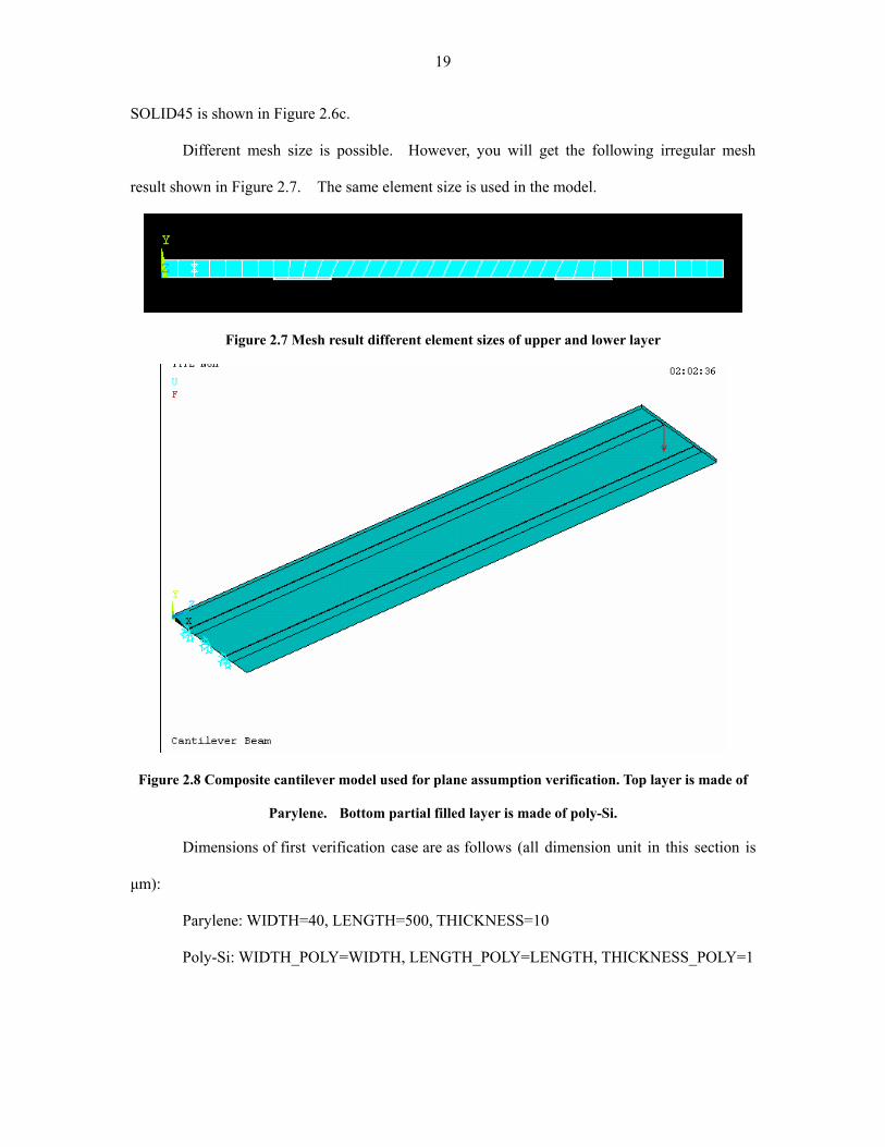
FIGURE 2.7 MESH RESULT DIFFERENT ELEMENT SIZES OF UPPER AND LOWER LAYER..................................... 19
FIGURE 2.8 COMPOSITE CANTILEVER MODEL USED FOR PLANE ASSUMPTION VERIFICATION. TOP LAYER IS
MADE OF PARYLENE. BOTTOM PARTIAL FILLED LAYER IS MADE OF POLY-SI. ....................................... 19
FIGURE 2.9 ELEMENTS PLOT FOR VERIFICATION CASE 1 (ELEMENT SIZE 5). TOP LAYER IS MADE OF PARYLENE.
BOTTOM THIN LAYER IS MADE OF POLY-SI. LEFT SIDE IS THE FIXING END. STRAINS AT THE TOP OF THE
PARYLENE LAYER (NODE 1134) AND AT THE BOTTOM OF POLY-SI LAYER (NODE 2837) ARE OF INTEREST.
............................................................................................................................................................. 20
FIGURE 2.10 STRAIN RESULTS OF DIFFERENT NODES FROM THE FIXING END. THE CONTINUOUS LINE IS FROM
ANALYTICAL RESULT. A) STRAIN AT THE TOP OF THE CANTILEVER (PARYLENE); B) STRAIN AT THE
BOTTOM OF THE CANTILEVER (POLY-SI)................................................................................................ 22
FIGURE 2.11 DIRECT VISUALIZATION OF THE DISPLACEMENT OF A CROSS SECTION. A) THE CROSS SECTION IS

1
1 Introduction
DNA sequencing is the process of determining the nucleotide order of a given DNA
fragment. For thirty years most of the DNA sequencing has been done using the chain
termination method that was developed by Frederick Sanger [1]. However, Sanger method has
inherent speed and cost limitations [2]. Trying to overcome limitations, many alternative
methods have been conceived and investigated such as pyrosequencing [3, 4], sequencing by
hybridization [5-7], by time-of-flight mass spectrometry [8], and by single molecule methods.
The DNA sequencing based on single molecule methods has attracted considerable attentions due
to several highly desirable advantages. First, single molecule DNA sequencing enables the
determination of nucleotide sequence using a single or a few DNA molecules. Therefore, it
eliminates the time-consuming and laborious cloning and amplification steps. Second, the Sanger
method has an upper read-length limit of ~1000 bases whereas the single molecule methods do
not have such a limit. Third, the sequencing rate can reach hundreds of bases per second or even
higher. Up to now, single molecule DNA sequencing approaches include methods based on
fluorescence labeling, atomic force microscopy (AFM), and ion current detection through
nanopores. Despite some progresses, these methods still have several challenging obstacles to
overcome before achieving the final goal of practical single molecule DNA sequencing.
In an attempt to circumvent the limitations of current approaches, an innovative
Lab-on-Tip nanomechanical platform, with several unique advantages, is proposed for single
molecule DNA sequencing. This novel approach is based on the fact that the unbinding forces
between DNA nucleotides are different, with G-C pair of ~20 pN (pico-Newton) and A-T pair of
~10 pN. This new Lab-on-Tip approach combines the advantages of existing single molecule
DNA sequencing methods but decreases the difficulty of technical challenges of each method
when they are employed individually.
The main achievement of the thesis is the successful development of a prototype of the

2
Lab-on-Tip testing platform with pico-Newton force resolution, which is good enough for
aforementioned DNA sequencing and other applications as nanotribology, biomechanics and so
on. The mechanics model of the composite cantilever, fabrication process, testing platform
configuration and testing result analysis are elaborated in Chapters two to five. In the
introduction chapter, three different catalog sequencing methods are explained and compared first,
following by a detailed explanation of the new Lab-on-Tip method.
1.1 The fluorescence based method
The fluorescence method is based on the detection of individual fluorescent dyes attached
to nucleotides in a flowing sample stream [9, 10]. A typical protocol consists of following steps:
(1) the DNA to be sequenced is copied using nucleotide triphosphates (dNTPs) that are labeled
with two or more different fluorescent dyes; (2) the 5’-end of DNA is immobilized on a
microsphere or tip of a fiber, and then suspended in a flowing buffer stream; (3) an exonuclease is
added in the flow stream to start the sequential cleavage of fluorescent monophosphate molecules
(dNMPs) from the 3’- to the 5’-end of the DNA; (4) the cleaved dNMPs are transported to the
detection area downstream sequentially. The DNA sequence can be obtained by identifying each
individual fluorescent dNMP molecule using single-molecule fluorescence spectroscopy.
However, complete substitution of natural dNTPs by dye labeled dNTPs has not yet been
achieved. This is because the steric hindrance at the polymerase active site prevents full
replacement of natural dNTPs by the modified analogues [11].
1.2 The AFM based method
The second single molecule DNA sequencing method is based on different binding forces
between complementary DNA nucleotides: adenine (A), cytosine (C), guanine (G), and thymine
(T). In most cases, atomic force microscopy (AFM) [12] is employed to measure the pN level
unbinding forces of A-T and G-C pairs. A typical AFM system consists of a micromachined

3
cantilever with a sharp tip, a laser source, and a position sensitive detector (PSD) to sense the
reflected laser beam from the end-point of the cantilever.
Boland et al. coated purines and pyrimidines on both planar gold surface and AFM tip
and then directly measured the intermolecular hydrogen bonding in DNA nucleotide bases by
probing the gold surface with AFM tip [13]. The different binding forces between A-T and G-C
pairs were measured. They also found out that hydrogen bonding between the tip molecules and
surface molecules can only be measured between complementary bases, i.e., A-T and G-C.
However, it is difficult to use nucleotide coated AFM to sequence DNA because of the limited
spatial resolution.
The binding forces of G-C and A-T pairs can also be measured by unzipping
double-stranded DNA [14, 15]. For example, Rief et al. [15] unzipped the hairpins formed by
poly (dG-dC) and poly (dA-dT) DNA with AFM and directly revealed the unbinding forces of
G-C pairs and A-T pairs, which are 20 pN and 10 pN respectively. It has been proposed that this
unbinding force could be useful in single molecule sequencing [14-16]. To date, the best
resolution achieved by this method (mechanical unzipping) is ~500 bases [14]. The major
limitation of this unzipping approach is the longitudinal elasticity of the already sequenced single
strand sections, which soften the displacement-force function and facilitate spontaneous thermal
opening of the base pairs [16].
1.3 The method based on the ion current detection through
nanopores
It was observed that when a DNA strand traversed a nanoscale pore under an electrical
field, the ion current through the nanopore is modulated by the nucleotides. A single molecule
DNA sequencing method has been proposed based on this phenomenon [17]. This approach
requires a pore that ensures single-file, unidirectional transport of DNA strands across a defined
aperture at nanometer precision. To date, the best candidate is the pore formed by α-hemolysin,

4
a 33 kD protein isolated from Staphylococcus aureus, which self-assembles in lipid bilayers to
form a channel with a nanoscale pore, as shown in Figure 1.1[18]. The mouth of the channel is
about 2.6 nm in diameter. The pore then widens into a vestibule that abruptly narrows to a
limiting aperture of 1.5 nm, which is just larger in diameter than an extended single strand of
DNA, at about the membrane-solution interface. It has been demonstrated that single stranded
DNA or RNA molecules can be detected when they traversed the α-hemolysin nanopore by
monitoring the ionic current through the nanopore [17, 19-28]. Several novel fabrication
processes have also been conceived to fabricate solid-state nanopores with diameters of a few
nanometers for DNA sequencing [29-31].
Figure 1.1 Single α-hemolysin channel embedded in a lipid bilayer. A single strand of poly(dC) DNA
is being driven through the pore by the electrical field applied [18].
However, as explained in [18] and [32], detection of ion current through the α-hemolysin
pore or solid-state nanopores probably is not able to yield DNA sequence at single-nucleotide
resolution for two reasons. First, the narrowest portion of the α-hemolysin pore is 5 nm long
(solid-state nanopores are much longer), meaning that at a given instant there are approximately
seven nucleotides block the nanopore. Each of those seven nucleotides would contribute to
resistance against ionic current, thus obscuring the influence of any single nucleotide. Second, the
number of monovalent ions flowing through the narrowest segment of the pore during ssDNA
translocation is very small. It has been estimated that the current difference between single
cytosine (C) and adenine (A) nucleotide is at most 100 monovalent ions, a level that cannot be

5
discerned [18].
1.4 Single molecule DNA sequencing based on a Lab-on-Tip
nanomechanical platform
Figure 1.2 (a) The schematic drawing of the Lab-on-Tip device. Nanofluidic components are
integrated on the tip. Lateral pN force can be translated to the bottom cantilever and be detected by
optical lever method; (b) blowup of the nanofluidic component (two reservoirs and one lateral
nanopore) on the tip; (c) schematic illustration of one ssDNA passing the nanopore and interacting
with probe molecules immobilized on the outlet surface of the nanopore
Here, in an attempt to circumvent limitations of current methods, a novel Lab-on-Tip
nanomechanical platform, as shown in Figure 1.2, is proposed for DNA sequencing at single
molecule level. This novel approach is based on the fact that the unbinding forces between
complementary DNA bases are different, i.e. 20pN for G-C and 10pN for A-T [13, 15]. The

6
Lab-on-Tip device is constructed by forming a vertical pole on a lateral cantilever beam. On the
tip of this vertical pole, a lateral nanopore and two solution reservoirs will be integrated as shown
in Figure 1.2(b). Probe molecules (e.g., DNA nucleotides) are immobilized on the outlet surface
of the nanopore (Figure 1.2(c)).
One of the reservoirs is filled with the diluted target ssDNA solution and the other is
filled with buffer solution. The ssDNA molecule can be threaded into the nanopore by applying
an electrical voltage between the two reservoirs. The established electrical field will
automatically drive the charged ssDNA molecule into the nanopore. This simple self-threading
process has been demonstrated by many researchers. Since the unbinding forces between DNA
nucleotides and probe molecules are different, when the target ssDNA traverses the nanopore,
different lateral forces will be generated. The force is amplified and translated to a
nanomechanical deflection of the bottom cantilever via the vertical pole. The deflection of the
bottom cantilever is then detected by optical lever method or by piezoresistor, just like AFM, with
a pN resolution. Therefore the DNA could be sequenced by monitoring the lateral forces as the
DNA strand passes the nanopore. This is equivalent to using a nano-ring to “scan” the DNA
molecule. Figure 1.2(c) schematically illustrates the scenario in which a target ssDNA is
passing the nanopore and interacting with the probe molecules immobilized on the outlet surface
of the nanopore.
In addition to the advantages common to single molecule DNA sequencing, the approach
possesses several unique features. This new Lab-on-Tip approach combines the advantages of
the nanopore (based on ion detection) and AFM methods but decreases the difficulty of technical
challenges of each method when they are employed individually. For example, since force
sensing is employed, the nanopore of the Lab-on-Tip device does not have to be so small to just
allow the traverse of DNA while blocking the ion current. Therefore solid state nanopores,
rather than biological ones, with diameters greater that 20nm can be used. Such solid state
nanopores are less challenging to fabricate. In this new scheme, the ultimate spatial resolution is

7
determined by the thickness of the probe molecule layer, not the length of the nanopore. Thus a
much better resolution, eventually single nucleotide resolution, can be realized. In addition, this
new approach solves the tracking or alignment problem of AFM based method since the ssDNA
molecule is threaded into a nanopore. Compared with the fluorescent method, this new
approach eliminates the labeling step.

8
2 Structure analyses for composite beams
In order to maximum the sensitivity, a soft material (i.e. small Young’s modulus) is
preferred for cantilever fabrication. Parylene, whose Young’s modulus is only ~3Gpa, is proved
to be a practical MEMS material and is used for our cantilever For such one layer MEMS
cantilever beam, analytical solution is accessible [33]. If the optical lever is used to detect the
cantilever deflection, the other metal layer needs to be coated to reflect light. If the piezoresistor
is used, a piezoresistive layer (e.g. poly-Si) is required besides cantilever itself. For both cases,
the beam is made of at least two different materials with large Young’s modulus and Poisson ratio
variation. For such laminated cantilever, extension of analytical solution is possible [34, 35, 36].
But, all above papers actually suggest one layer is covered 100% by another layer. Their
equation is also not validated in the case for such large Young’s modulus variation (Young’s
modulus for Parylene: ~3Gpa; for Si: 168Gpa). Thus it is necessary for us to develop step by
step the analytical model and validate the model by FEM results.
This chapter deals with so called structure analysis, which incorporates the fields of
mechanics, dynamics, and the many failure theories required to study and predict the behavior of
structures. The primary goal of structural analysis is the computation of deformations, internal
forces and stresses. To perform an accurate analysis one must determine such information as
structural loads, geometry, support conditions, and materials properties. Advanced structural
analysis may examine dynamic response, stability and non-linear behavior.
There are three approaches to the analysis: the mechanics of materials approach (also
known as strength of materials), the elasticity theory approach (in fact a special case of the more
general field of continuum mechanics), and the finite element approach [37]. The first approach
leads to second order ordinary differential equations and thus closed-form analytical solutions.
Though its structural elements and loading conditions are relatively simple, the result appears
accurate enough for most practical MEMS cases and is most widely used. The elasticity

9
approach leads to second order PDE (Partial Differential Equation). Though this approach
allows the solution of structural elements of general geometry under general loading conditions,
the analytical solution is limited to relatively simple cases as one may expect from previous
knowledge of PDE. The last one is actually a numerical method for solving differential
equations that are generated by the first two methods.
Regardless of approach, the formulation is based on the same three fundamental relations:
equilibrium, constitutive, and compatibility. Solutions are approximate when any of these
relations are only approximately satisfied. Based on the mechanics of materials approach, a
closed-form analytical solution is derived with several assumptions in Chapter2.1. These
assumptions (e.g. plane assumption that result in the compatibility equation) and the analytical
solution are verified by a finite element model in Chapter 2.2.
2.1 Analytical model for composite beams
Research objects of mechanics of materials approach are all kinds of beams[37].
Fabrication processes of MEMS cantilevers belong to surface micromachining, which implies
MEMS cantilevers more likely belong to shell elements not beam elements [38]. However, the
beam model is still used here for its simplicity comparing with shell and plate models in elastic
mechanics. Further, various real applications show that simple beam model is already good
enough for most cases. This analytical model will be verified later by an FEM model.
For a composite beam shown in Figure 2.1, the resultant momentum and force in one
cross section can be decomposed to Mx, My, Mz, FNx, FQy and FQz. For our application, only
normal stress is of concern. Thus no Mz, FQy and FQz components will appear in later analyses.

10
Figure 2.1 Schematic beam model for normal stress analysis with resultant momentum and force in
one cross section
In general, the effect of resultant force and momentum is the superposition of their
coordinate components’. If transverse sections of the beam which are plane before bending will
remain plane during bending as shown in Figure 2.2, the compatibility equation of deformation is
written as:
0 ( ) ( )z ydu du y d z dθ θ= − + 2.1)
In derivation of Eq.2.1, we also suggest that transverse sections will be perpendicular to
circular arcs with a common centre of curvature and the radius of curvature is large compared
with the transverse dimensions. The corresponding normal strain is:
0xz y
du y zdx
ε ερ ρ
= = − + 2.2)
Where, by definition, 00
dudx
ε = , yy
dxd
ρθ
= , zz
dxd
ρθ
= . 0ε , yρ and zρ need to be
decided later.

11
Figure 2.2 Schematic plot of geometry used to derive compatibility equation
If linear constitution law (Hooker’s law) is suggested, we have
0( , ) ( , )( , )x
z y
E y z E y zE y z y zσ ερ ρ
= − + 2.3)
Here symbol ( , )E y z is used as the Young’s modulus of the composite beam is the
function of position y and z. Now we put this constitution law in the force equilibrium equation.
x NAdA Fσ =∫ , ( )x yA
dA z Mσ =∫ , ( )x zAdA y Mσ = −∫ ,
01
N i i i zii i z
F E A E Sερ
= −∑ ∑ 2.4)
0
0
( )( )
1 1
zz yA
i zi i zi i yzii i iz y
y zM E y dA
E S E I E I
ερ ρ
ερ ρ
= − − +
= − + −
∫
∑ ∑ ∑ 2.5)
where by definition zi AiS ydA= ∫ , 2
zi AiI y dA= ∫ and yzi Ai
I yzdA= ∫ . If the
structure is symmetry with y axis (for most applications it is), we have 0i yzii
E I =∑ because for

12
every layer we have 0yziI = .
If 0i zii
E S =∑ , which means y=0 should be the neutral layer, we get
0N i ii
F E Aε=∑ 2.4’)
1z i zi
i z
M E Iρ
=∑ 2.5’)
All first moments of an area and moments of inertia of an area are calculated about the
neutral center. We may start with an arbitrary Y coordinate (of course origin of Z should be the
symmetry center), and write explicitly the equation for neutral plane as
i i cii
ci i
i
E A yy
E A=∑∑
, where i zi i i cii i
E S E A y=∑ ∑ 2.6)
We calculate the moment of inertia with respect to the layer’s own geometry center and
then move to the neutral plane as
20 ( )zi zi c ci iI I y y A= + − 2.7)
where yc is the position of neutral plane calculate from Eq.2.6, and yci is geometry center
of the ith layer.
The normal stress for composite materials now is obtained:
( ) ( ) ( )N zx c
i i i zi
F ME y E y y yE A E I
σ = − −∑ ∑
2.8)
Here the selection of the origin of y coordinate is arbitrary. We only need to calculate
the moment of inertia by Eq.2.7.
Mathematically for a smooth curve, if the deflection is w, its curvature can be expressed
as:

13
2
2
3/ 22
1
1z
d wdx
dwdx
ρ=⎛ ⎞⎛ ⎞+⎜ ⎟⎜ ⎟⎜ ⎟⎝ ⎠⎝ ⎠
2.9)
For small deflection, i.e. 2
2 1d wdx
<< , we have:
2
2
1
z
d wdxρ
= 2.9’)
Recall Eq.2.5’, we get 2
2z
i zii
Md wdx E I
= −∑
. 2.10)
Here the minus sign comes from the sign convention as described in [37].
Thus the tip deflection angle is
z
i zii
M Ldwdx E I
θ = = −∑
2.11)
where L is the beam length.
2.2 FEM model and validation of analytical solution
Eq.2.8 connects external forces with internal forces, and thus the external equilibrium
analysis with internal equilibrium analysis at large. Several assumptions are made before we get
here:
1. Supposition: the effect of resultant force and momentum is the superposition of their
coordinate components’;
2. No lateral stress: longitudinal elements of the beam are subjected only to simple
tension or compression;
3. Plane assumption: transverse section of the beam which is plane before bending will
remain plane during bending;

14
4. Small deformation: transverse sections will be perpendicular to circular arcs having a
common centre of curvature and radius of curvature is large compared with the transverse
dimensions;
5. Linear constitutional law.
We do not challenge small deformation at this time. Actually it is a reasonable
assumption in most MEMS structures. In many cases the material itself is unable to experience
large deformation. Linear constitutional law can be relaxed either in the derivation we consider
this non-linear relationship or we use energy analysis (e.g. virtual force, Moire integration, etc.).
For small deformation, linear constitutional law fits experimental results well. Thus we do not
need to worry about it for aforementioned two reasons.
Usually item2 is not satisfied if the bending momentum is generated from a force. Also,
different Poisson ratio of different layer will also generate in-layer shearing force.
As for the plane assumption, we need more discussions. This method was proposed for
the analysis of normal stress in beam. Beam itself is an ambiguous definition in mechanics of
materials. If we call something beam, probably we mean it experiences bending momentum.
As an analogy, if we call something axis, it must experience torque. Another criteria make plane
assumption questionable are too much difference in Young’s modulus (range from 3GPa to
168GPa) and Poisson ratio (from 0.4 to 0.22) (see Appendix B) of our materials. In this section,
we shall first study from a theoretical viewpoint the validity of our model, and then present
several FEM models for final verification.
2.2.1 Theoretical validation
According to symmetry analyses, we can prove that after deformation, the cross section
remains plane after deformation. Take an example of a beam experiences pure bending in Figure
2.3. As the requirement of symmetry, any point in the cross section A-A should not have
displacement along X axis. Thus cross section A-A remain plane after deformation.

15
Figure 2.3 Schematic plot for validation of plane assumption of a beam under pure bending
If we cut the beam along A-A, the left two beams experience the same external
momentum as that of the original beam. The conclusion holds. Keep on this process and we
can prove under pure bending Mz, all the plane after deformation will remain plane. Same
conclusion holds for beam under My and FNx.
Without shearing force, key equation is in good agreement with experiment results. In
the case of shearing force exists (FQ), plane assumption is not valid and key equation’s prediction
may vary from experimental result. But, if the length dimension is much larger than beam height
and width, experimental results show such difference is minor and generally can be ignored.
Thus our equation is also applicable when shearing force exists.
Figure 2.4 Geometry used for comparisons of shearing force and normal force in a beam

16
For rectangular beam, we have 2
max
max
6
432
P
P
F llbh
F hbh
στ
= = .
For round beam, we have 3
max
max2
32
6443
P
P
F lld
F dd
σ πτ
π
= =
How the load is applied may play a role here. Sainte-Venant principle predicts: for sold
beam structure, if two loads is equivalent in sense of static, the stress different in the realm a little
bit far from loading point should have only minors difference. However, it is not true for thin
shell beam as shown in Figure 2.5. Experimental results show now the effect of loading will
affect the whole beam. For such kind of thin-shell structure, limited analytical results are
available.
Figure 2.5 Structure manifests loading effects. a) Solid structure; b) Thin shell
All the previous discussions are in the realm of mechanics of materials. It features easy
of use and accurate enough for most engineering applications. Another discipline called
“elasticity” features application of uniformed methods to handle any form of problems. It is
based on the solution of PDE (partial differential equation) with certain boundary conditions.
With this method, one may discard the aforementioned plane assumptions. However, the

17
problem for this method is you can not have analytical result. You may only get numerical
results using FEM or FDTD or material points and etc. We developed an FEM model in next
section and use the solution of elasticity for validation of our previous analytical results.
Experimental results have the final word. If we have question concerning one structure,
we should do experiments to validate our analytical and numerical results. For our micro
structure, we may scale it to do some experimental analysis if possible.
2.2.2 FEM models
As for the layered structure, if the covering ratio is 100% or large enough, intuitively
plane assumption should be valid. If the covering ratio decreases, how do we apply load plays a
role here. An FEM model is built to verify our analytical model.
One key question in FEM model is what kind of elements to choose from. To verify
plane assumption, we must have several nodes in the cross section. In theory the cantilever
belongs to shell as the thickness is much smaller compare to width and length [38]. Ansys did
supply shell elements, even including layered shell elements such as SHELL91 and SHELL99.
However, as Figure 2.6a shows, one shell element only has only one center node output in the
thickness direction, which is incapable to validate plane assumption. Further, such structure
actually suggest the covering ratio to be one for all the different layers, thought different layers
may contain different material properties. Situation for solid layered elements such as SOLID46
is similar as shown in Figure 2.6b, where we have only corner elements output thought we may
have different layers. What’s more, SOLID46 did suggest all covering ratio to be 100%.

18
a)
b)
c)
Figure 2.6 Geometry of FEM elements used in ANSYS model [39] a) SHELL99 b) SOLID46 c)
SOLID45
As all the layered elements in Ansys suggest 100% covering ratio, we can not use such
layered structure for our analysis. The elements I used were SOLID45 and SOLID95.
19
SOLID45 is shown in Figure 2.6c.
Different mesh size is possible. However, you will get the following irregular mesh
result shown in Figure 2.7. The same element size is used in the model.
Figure 2.7 Mesh result different element sizes of upper and lower layer
Figure 2.8 Composite cantilever model used for plane assumption verification. Top layer is made of
Parylene. Bottom partial filled layer is made of poly-Si.
Dimensions of first verification case are as follows (all dimension unit in this section is
µm):
Parylene: WIDTH=40, LENGTH=500, THICKNESS=10
Poly-Si: WIDTH_POLY=WIDTH, LENGTH_POLY=LENGTH, THICKNESS_POLY=1

20
Figure 2.9 Elements plot for verification case 1 (element size 5). Top layer is made of Parylene.
Bottom thin layer is made of poly-Si. Left side is the fixing end. Strains at the top of the Parylene
layer (node 1134) and at the bottom of poly-Si layer (node 2837) are of interest.
Nodes used for verification locate 50µm far from the fixing end (left end in Figure 2.8
and Figure 2.9). Theoretical strain results are (according to Eq.2.6): Strain_top = 1.0517e-004;
Strain_bottom = -1.4507e-005. FEM results are 0.31540E-06/0.003 = 1.0513e-004 and
0.24395E-05/0.168 = 1.4521e-005. The relative error is less than 0.1%.
As known, when the meshing size becomes smaller and smaller, FEM result itself should
convergent. However, we must compromise the computation time with the precision. To make
sure the mesh is dense enough, one simple way is shrink the mesh by factor of 2 and see if there
is acceptable output difference. For data set 2 in Table 1, if we change the mesh size from 5 to
2.5, the maximum displacement at the tip will go from 30.919 to 30.951, which means our mesh
size is already good enough.
We did several other verifications and the results are shown in the following table:
Table 1 Cantilever Length=500, element size 5. Data set 1-4 use the same Poisson ratio; data set 5

21
and 6 use different Poisson ratio. Data set 1-3 use force 1e-6N; data set4-6 use force 1e-7N
(W=Width, T= Thickness)
Parylene poly-Si Strain at point 1 Strain at point 2 Data
Set W T W T Theory FEM Theory FEM
1 40 10 40 1 1.0517e-004 1.0513e-004 -1.4507e-005 -1.4521e-005
2 40 3 40 0.5 0.0010 0.0010 -1.4127e-004 -1.4210e-004
3 40 5 40 0.5 4.2070e-004 4.2137e-004 -5.8164e-005 -5.8226e-005
4 100 3 20 0.5 4.7421e-005 4.8507e-005 -1.5459e-005 -1.5691e-005
5 100 3 20 0.5 4.7421e-005 4.8707e-005 -1.5459e-005 -1.5518e-005
6 310 3 10 0.5 2.0974e-005 2.3964e-005 -1.7561e-005 -1.8485e-005
As one may see from Table 1, when covering ratio is large (e.g. 0.2), our analytical
results agree very well with FEM model. When the covering ratio decreases further, relative
error may reach 15% (corresponding covering ratio 0.03). The analytical model did not count in
the effect of Poisson ratio. FEM results show actually for the nodes a little far from the fixing
end, the effect of Poisson ratio is not pronounced. However, this is not true for the nodes near to
the fixing end. Now we study different position points from the fixing end. Geometry and
loading is the same as in data set 4. The results are shown in Figure 2.10.

22
a)
b)
Figure 2.10 Strain results of different nodes from the fixing end. The continuous line is from
analytical result. a) Strain at the top of the cantilever (Parylene); b) Strain at the bottom of the
cantilever (poly-Si)

23
As shown in Figure 2.10, FEM result shows well agreement with our analytical model
except at the point very near to the fixing end. It is because the fixing end also confines the
transverse displacements due to Poisson ratio. For this area, analysis shows we should use
Young’s modulus 2/(1 )E v− instead [36] to get better analytical results. For this marginal effect
to be pronounced, we found 0.3*Width is a criteria, which means if width=100µm, 30µm is the
break point.
From Figure 2.10b, we see the real strain of poly-Si is smaller than theoretical estimation
when a little far from the fixing end. This is accordant with our intuition.
The strain and displacement results agree well with the analytical model we derived
before. This partially validates the assumptions we made before. Actually we may directly
visualize plane assumption. As shown in Figure 2.11, when the cross section is a little far from
the fixing end, plane assumption is validate. This is not true when the cross section is very near
to the fixing end (e.g. 5µm in Figure 2.11b). It also explains why there are large errors of
analytical results in these areas.
a)

24
b)
Figure 2.11 Direct visualization of the displacement of a cross section. a) The cross section is 50µm
from the fixing end. b) The cross section is 5µm from the fixing end
3 Fabrication
Our devices’ dimensions are schematically shown in Figure 3.1. Central pole and tip
reflector are both squares with edge length ranging from 200µm to 400µm. The cantilever length
is 300µm for all cantilevers.

25
Figure 3.1 Dimensions of cantilevers (unit: µm), square central pole height: 500µm
Several fabrication processes for the device were developed. Two processes will be
discussed separately later. For both process backside alignment is required.
3.1 Fabrication process 1
The initial fabrication process is shown in Figure 3.2. Two batches of devices were
fabricated with the first process.
a)
b)
Figure 3.2 a) Simplified fabrication process; b) Three masks used for the process (from left to right:
mask1, mask2 and mask3)
First 0.1µm Aluminum was evaporated on the backside of a 5-inch Silicon wafer
3. Etch through from the frontside using DRIE, freeing the cantilever. Remove parylene layer.
1. Deposit and pattern 0.1µm aluminum layer (mask2) and parylene C layer on the backside of the wafer.
2. Deposit and pattern 0.1µm aluminum layer (mask1 and 3) on the frontside of the wafer.

26
followed by 2.2µm Chemical Vapor Deposition (CVD) of Parylene C. Adhesion promoter
(A-174 Silane) was applied to the wafer before the Parylene deposition. 10µm photo resist (AZ
4620) layer was spin coated on the backside of the wafer and soft baked for 1 minute at 110°C on
a hot plate. The wafer was exposed using a dark field mask for 28 seconds under the UV light.
Later the wafer was developed using AZ 400K developer. The wafer was then hard baked for 5
minutes at 120°C on a hot plate. Oxygen plasma was used for 18 minutes at 100 Watts (oxygen
flow rate 35 sccm) in the Dry Tek RIE system to etch away Parylene C. Parylene C was
removed form the front side completely using RIE. Later the underneath Aluminum layer was
etched using wet etching. Finally the photo resist was removed using acetone, alcohol and water.
0.1µm Aluminum was evaporated on the front side of the wafer. Using photo resist as the mask
(Shiply’s S1811 spin coated at 4000 rpm for 30 sec, 1µm thick) the aluminum was patterned by
wet etching. Finally the wafer was etched through using Deep Reactive Ion Etching (DRIE) to
form freestanding cantilevers with micro pole. The process was repeated with 2 masks to form a
50µm thick rectangular wall.
AutoCAD is used to draw the masks. To get the filled pattern output as post script (PS)
file, one must fill the isolated pattern (e.g. the small square in Figure 3.2) in AutoCAD manually,
which is an extremely tedious job. Some third party software such as LinkCAD can do this
automatically. However, it is possible to stick with AutoCAD and do some advanced
development to solve the problem. The DXF output file of AutoCAD was studied and a C
program was drafted to do the job automatically. Basically the program will fill all the closed
polyline on a specific layer. With this framework, one may even fill any area or any shape of the
object specified, which offers much more flexibility than commercial software such as LinkCAD.
Parylene polymers are deposited from the vapor phase by a process, which in some
respects is similar to vacuum metallization Unlike vacuum metallization, however, which is
conducted at pressures of 10-5 torr or below, the Parylenes are formed at around 0.1 torr. Also,
Parylene deposition is a conformal coating process.
27
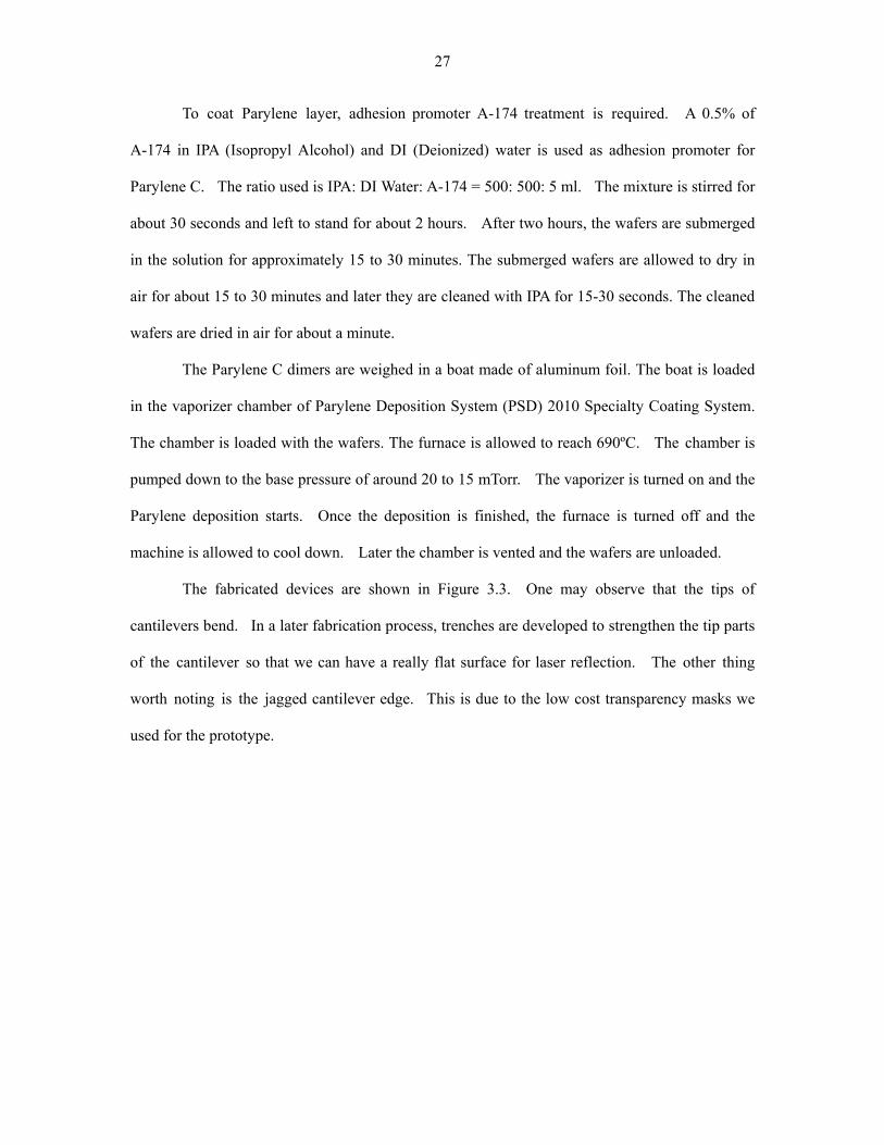
To coat Parylene layer, adhesion promoter A-174 treatment is required. A 0.5% of
A-174 in IPA (Isopropyl Alcohol) and DI (Deionized) water is used as adhesion promoter for
Parylene C. The ratio used is IPA: DI Water: A-174 = 500: 500: 5 ml. The mixture is stirred for
about 30 seconds and left to stand for about 2 hours. After two hours, the wafers are submerged
in the solution for approximately 15 to 30 minutes. The submerged wafers are allowed to dry in
air for about 15 to 30 minutes and later they are cleaned with IPA for 15-30 seconds. The cleaned
wafers are dried in air for about a minute.
The Parylene C dimers are weighed in a boat made of aluminum foil. The boat is loaded
in the vaporizer chamber of Parylene Deposition System (PSD) 2010 Specialty Coating System.
The chamber is loaded with the wafers. The furnace is allowed to reach 690ºC. The chamber is
pumped down to the base pressure of around 20 to 15 mTorr. The vaporizer is turned on and the
Parylene deposition starts. Once the deposition is finished, the furnace is turned off and the
machine is allowed to cool down. Later the chamber is vented and the wafers are unloaded.
The fabricated devices are shown in Figure 3.3. One may observe that the tips of
cantilevers bend. In a later fabrication process, trenches are developed to strengthen the tip parts
of the cantilever so that we can have a really flat surface for laser reflection. The other thing
worth noting is the jagged cantilever edge. This is due to the low cost transparency masks we
used for the prototype.

28
a)
b)
Figure 3.3 Micrograph of two Lab-on-Tip devices a) Topside pole b) backside cantilever

29
3.2 Fabrication process 2
After the fabrication of the first batch of the lab on tip devices, we decided to alter the
fabrication process to reduce the mass of the pole, which was made of silicon in the first round
device. Also, trenches were added to form flat cantilever for laser beam reflection. Thus the
fabrication process was altered in to the following manner shown in Figure 3.4:
1. Wet thermal oxide was grown on a double side polished wafer for one hour,
forming a half-micron thick silicon oxide layer.
2. Using Photo resist, 1811, as the mask, the oxide layer was patterned using a
buffer oxide etch solution (BOE). Mask one was used in this process to make trenches on one
side of the wafer. A layer of Photo resist is coated on the other side of the wafer to protect the
oxide layer on that side. The trenches were introduced in the design as an attempt to form a flat
end on the lower cantilever structures by introducing strong mechanical structures provided by
the trances, which will later be coated by Parylene C, deposited using CVD technique.
3. Cavities are formed on the other side of the wafer by using mask 2, photo resist
as the mask layer and BOE as the etching solution for the oxide layer. A layer of Photo resist is
coated on the other side of the wafer to protect the oxide layer on that side.
4. Once the oxide on both sides of the wafer was patterned, the Photo resist layer
was stripped and the wafer was dipped in the TMAH solution for one hour to etch trenches in
silicon, which were approximately 10 microns deep.
5. Steps 1 through 4 are replaced by using photoresist as a mask layer and just using
DRIE 10 loops to etch trenches 7 – 8 microns deep on silicon wafers.
6. After the trenches were formed, thin film of Aluminum (30 nm) was evaporated
on both sides of the wafer.
7. Aluminum at the side of the wafer with the trenches is patterned with the
cantilevers using mask 3, photo resist 1811 as the mask layer and etched using the aluminum

30
etching solution. A layer of photo resist is coated on the other side of the wafer to protect the
aluminum layer on that side.
8. On the other hand, Aluminum on the other side of the wafer is patterned using
masks 4. A layer of photo resist is coated on the other side of the wafer to protect the aluminum
layer on that side. Mask 4 is the pattern, which will be used to etch a long perpendicular pole on
the cantilevers.
9. A thick layer of Parylene C (10 microns) is deposited on the wafer using the
Parylene Deposition System (PDS).
10. Parylene is removed from, the front side of the wafer using oxygen plasma
(Oxygen flow rate 35 sccm, power 200 W).
11. The wafer is etched through using Deep Trench Etcher ( DRIE ).
12. A thin layer of Parylene C (2 microns) is deposited to cover the top side of the
wafer wehre silicon poles are made by DRIE.
13. Aluminum is sputtered on the topside of the wafer s a mask layer to etch
Parylene off from the backside.
14. Parylene is etched from the back side using Oxygen plasma in RIE.
15. Finally, silicon is removed from the poles using XeF2 dry etching technique for
silicon.

31
a)
b)
Figure 3.4 a) Alternative fabrication process; b)Four masks used for this process

32
4 Testing configuration
In order to test the sensor, we need a force generator, an optical lever and a testing
platform for data acquisition and processing. Chapter4.1 discusses how to generate tunable
pico-Newton force. Chapter4.2 and 4.3 deal with optical lever. An FEM model of Lab-on-Tip
device is constructed in Chapter4.4 to cross verify the testing results. Chapter4.5 and 4.6 focus
on the data acquisition and process based on virtual instruments.
4.1 tunable Pico-Newton force generation
The device is supposed to be able to resolve for pica-Newton lateral forces. To character
the device, we need to generate tunable pica-Newton forces at the tip of the pole (very small area,
e.g. several 100µm2).
4.1.1 Hall effect and Lorenz force
Hall effect was discovered in 1897. As the advance of semiconductor material and
technique, many new materials with high Hall coefficient appeared, such as N type Ge, InAsP,
and etc. Traditionally, Hall effect sensor is applied to measure the magnetic field strength. Its
measurement ranges from 10-9T [40] to 10T and its sensitive area can be less than 10µm2. Since
many semiconductors have high Hall coefficient, Hall effect is also widely used to measure their
carrier concentrations [41]. Here we suggest using Hall effect as a tunable force generator in
testing of Lab-on-Tip device, which is sensitive to pico-Newton force.
If an electric current flows through a conductor (or semiconductor) in a magnetic field,
the magnetic field exerts a transverse force on the moving charge carriers which tends to push
them to one side of the conductor.

33
Figure 4.1 Schematic illustration of Hall effect
If Hall sensor size is 10µm*5µm*1µm, the section area is 25 mA µ= . BnqvF dm = ,
dv is the drift velocity of the charges, n is the density of charge carriers and q is the charge of
one carrier (1.6*10-19). The density of charge carriers may be different from the impurity
concentration. However, as rough estimation, we may ignore their difference. The drift
velocity Id Ev µ= , whereµ is defined as mobility. Mobility is measure of ease of carrier drift.
Mobility in Si at room temperature depends on doping:
Figure 4.2 Mobility of electrons and holes versus doping concentration [41]

34
If doping concentration is 1013, then sVcm ⋅= /500 2µ (p-type). In the case voltage is
0.01mV, then smvd /05.0= .
If Fm=1pN, then B~10-5, corresponding to the magnetic strength of earth (5•10-5T).
In such doping concentration, the resistivity is around 103ohm•cm [41]. The resistance
is 2MΩ. nqdIBvH = , which is around 0.05mV. Thus the Hall voltage can be monitored easily.
We rewrite the force as HHdm EqnIdVvqnF µρ2222 / == ., where ρ is the resistivity.
Changing current I (thus the outer voltage) will change the force, which can be monitored by the
Hall voltage. The detailed parameters for such a device may be optimized to increase its
sensitivity and SNR (Signal to Noise Ratio).
It is not hard to fabricate Hall sensor. However, it is hard to connect the wires to the
Hall plate which resides in the pole tip. A more easy and direct method is wanted for our device.
4.1.2 Momentum of electromagnetic field and photonic pressure
From the wave viewpoint of light, if we suppose plane wave incident, the radiation
pressure on a perfect conductor is 22 cosiP w θ= , where iw is the average incident power and
θ is the incident angle [e.g. 42, 43].
From the viewpoint that light is ensemble of photon, it is possible to get the force
relationship using classical mechanics. Momentum of one photon is p0=E0/c, where E0 is the
photon energy and c is the light speed. If the laser power is P (mW) and illumination time is t,
Number of photon is n=Pt/E0. From Newton’s second law, we have Ft=2np0 (perfect reflection,
no heat). Thus F=2P/c, i.e. F=6.7P (pN), unit of P: mW.
In case of perfect absorption: F=3.3P (pN), unit of P: mW.
The real case is somewhere between 3.3P and 6.7P.
It is worth noting that the force is not related to the wavelength of the laser. In a more

35
accurate calculation, the absorption and the incident angle (around 15 degree) should be
considered.
4.2 Optical Lever
4.2.1 Criteria of reflective layer’s thickness
Electromagnetic wave decays exponentially in metals [44]. When conductor is present,
the propagation of electromagnetic wave is considered as a boundary problem, i.e. the
electromagnetic wave interact with the free charge in the conductor, which results surface current
and thus reflects incident wave. Surface current consumes energy and becomes Joule heat later.
For the thin layer conductor, the physics picture is somewhat like: part of the light is
reflected by the metal surface and the others are refracted in the metal. The refracted light
decays exponentially with respect to the penetration depth (the lost light becomes Joule heat). If
the metal layer is very thin, the refracted light will meet the other metal surface and experience
another reflection and refraction. The reflected wave may interfere with the reflect light from
the first surface, functioning as the Fabry-Pollet interferometer. The penetration depth and the
reflection coefficient of good conductor are calculate later, which give us a good insight of above
phenomena and the criteria of reflective layer’s selection at large.
Supposing 1) plane wave input, metal is large enough; 2) good conductor (the real part of
wave vector can be ignored); 3) perpendicular incidence, we have penetration depth as [44]:
0
1 2
r
δα ωσµ µ
= = , where ω is the light frequency, σ is the conductivity and rµ is
the relative permeability. In case of gold and aluminum, rµ is 1 and σ is 74.50 10× and
73.54 10× respectively. Thus for He-Ne laser (633µm), A 35u Aδ = and 39Al Aδ = . This
proves 300 A of Al is good enough to be considered as infinite thick layer. The corresponding

36
reflectance is [44]:
01 2 2 /R ωε σ≈ − , which is 93.2% for gold and 92.3% for Al. It proves we may
consider gold and aluminum as fairly good reflector in case of 633µm light incidence.
If the incident light is not perpendicular to metal surface, analysis shows the above
equation for penetration depth is still valid. As for the reflectivity, the calculation is somewhat
complex. We have to consider TE and TM mode in this case to calculate the reflectivity
separately. Please refer to [45, 46] for details.
4.2.2 Optical lever configuration
The real test platform and the schematic device are plotted in Figure 4.3a and Figure 4.3b
respectively. The laser beam is split into a sensing arm and a driving arm. Two beams are
separately focused on cantilevers by two focusing lens. An attenuator is added in the light path
of driving beam to control the driving power of the laser (thus tune the driving force). How to
choose the focal length and element spacing to achieve moderate spot size on Lab-on-Tip device
and PSD is the topic of next section.

37
Figure 4.3 (a) Picture of the testing setup of the Lab-on-Tip device; (b) schematic of the driving and
sensing scheme. Note one laser beam is used to drive the central pole. The other is used to sense the
deflection of the bottom cantilever.
4.2.3 Focusing lens selection and Gaussian beam
We have two different laser sources. For He-Ne laser, as its beam width and divergence
angle is quite small, any kind of lens that correct spherical and coma aberrations should be fine to
focus it. We may still use a zoom lens to bring us more flexibility in adjustments.
For He-Ne laser (model 1137 by Edmund optics), the beam divergence is 1.0mrad (full
angle) and the beam diameter is 0.81mm. Since such gas laser always offer very good beam
quality, we may suppose its M2 factor to be 1. Thus 3
0
0.5 10 radwλθ
π−= × = , 0 403w mµ= ,
which indicate the beam waist locate at the exit window of the He-Ne laser. If we suppose the
beam waist on cantilever is 50µm, i.e. 01 403w mµ= , 02 50w mµ= , we have [47-50]:
201
1 806Rwz mmπλ
= = ,201
2 12.4Rwz mmπλ
= = , resulting 0 1 2 100.0R Rf z z mm= = .
Thus the distance from first beam waist to the transform lens is
[47] 2 2011 0
02
' ' 125 8 75 725wz f f f mmw
= + − = + × = ; the distance from transform lens to the
second beam waist will be 2 2022 0
01
' ' 125 0.125*75 134wz f f f mmw
= − − − = − − = − .

38
Negative sign here means the other beam waist lay on different side of the lens.
For fiber pigtailed laser diode, however, we need to consider right optics to focus it.
First, zoom lens is still desired as the element spacing of our system can not be adjusted easily
due to the limitation of our optical table. To select a zoom lens, two important optical properties
must be specified: focal length range and F/#. F/# is decided by the aperture of the fiber we used.
For our SM600 fiber, average NA=0.12 (maximum value 0.14). Thus F/#=1/(2NA)=4.17 (min
value 3.57). In other word, the zoom lens’s F/# should be at least 3.5 to ensure all the light come
out of fiber can enter our system, i.e. no apodization.
Figure 4.4 Specifications of SM600 fiber (from Thorlab’s catalog)
The focal length range is decided by how large we want the focused spot to be and the
conjugate distance: i.e. the distance from fiber head to the focus point. For a perfect imaging
system (even without consideration of diffraction), if we want the spot size to be 50µm, the
magnification will be about 10. For our configuration, in case the conjugation distance ranges
from 300mm to 700mm, the focal lengths will be about 30mm to 70mm. Considering the
diffraction, the final size of the spot should be the convolution of airy spot (the diameter of airy
spot is 2.44*λ*F/#=60µm, F/# now is 10 times larger) with the 50µm disk, i.e. 170µm.
Actually even 170µm is hard to get for such lenses because we have to consider
aberrations, especially such photography lenses which usually are far away from diffraction limits
comparing with microscope and telescope objectives. Spherical aberration and coma should be
well corrected. However, aberration curves usually are not provided by manufacture. For a
rough estimation, if a CCD pixel size is 4µm, the requirement of MTF cutoff frequency is
1/(2*4µm)=125lp/mm, which is already beyond the industry standard for zooming lenses.
In all, optical requirements are F/#<3.5 and f ranges from 30mm to 70mm. A lot of

39
commercially available zooming lens fall the bin of focal length 30mm to 70mm. But, only
some high end zooming lenses satisfy F/#<3.5. We need select one from the high-end pool with
reasonable cost and really good imaging quality in the center area. Figure 4.5 shows such a
typical zoom lens design with zooming range from 28mm to 85mm and a constant F/# 4.
Figure 4.5 A typical zoom lens we used for ray-tracing verification. Focal length 28-85mm, F/# 4.
Green: 0.588(d), Blue: 0.486(F), Red: 0.656(C)
In our application, we need to invert the lens, i.e. our light source goes from film plane.
The flange focal distance (also known as the flange-to-film distance, flange focal depth, or
register, depending on the usage and source) of a lens mount is a very important parameter. This
is the distance from the mounting flange—the metal ring on the camera and the rear of the
lens—to the film plane. For Canon EF mount, flange focal distance is 42mm. The lens now
looks more like a zooming projection lens as shown in Figure 4.6.

40
Figure 4.6 Inverted zooming photographic lens for laser focusing. The conjugate distance is about
500mm, focal length 28mm. Wavelength is now specified as 633nm
It is obvious the lens is now far from diffraction limit. The corresponding spot diagram
is shown in Figure 4.7.
Figure 4.7 Spot diagram of the zooming lens. The black circle shows Airy spot size. Defocusing
from -25mm to 25mm.
From the spot diagram, the best spot size we can expect is about 200µm for this lens,

41
which is about the right size of our cantilever. The large aberration, especially the spherical
aberration results a large deviation of the spot size from Airy spot.
4.3 A complete ray-tracing model of optical lever
The calculation of the spot size on cantilever and the spot size on detector can be done
automatically with ray-tracing software such as OSLO, ZEMAX or CodeV. Ray-tracing
software can also help us to layout our optical system. The layout of our constructed model is
shown in Figure 4.8.
Figure 4.8 Layout of optical lever system
One may input the real size of the cantilever to observe diffraction effect. We draw the
spot-diagram as follows. The spot is not round because I artificially put the curvature of
cantilever as toric surface, which means it has two different curvature in X and Y direction as
shown in Figure 3.3b. The bottom of the spot is partially blocked by the cantilever reflector.

42
Figure 4.9 Spot diagram on detector
Gaussian beam analysis can be carried out with the same model. Every black straight
line means an optical surface defined in the spreadsheet. Figure 4.10 shows how the Gaussian
beam has been focused by the first imaging lens. From this interactive design, we may easily
find the precise position and size of the beam waist.
Figure 4.10 Interactive Gaussian beam analyses
4.4 FEM model of Lab-on-Tip devices
In this chapter, static, mode and harmonic analyses are performed using FEM model. It
seems that the resonant frequency can not be very high since the pillar is very heavy. But a

43
heavy pillar will not affect DC response.
A simple composite cantilever model is built for method verification. The dimensions
we used are as follows (all in µm): WIDTH=5, LENGTH=50, THICKNESS=2.3,
THICKNESS_Al=0.5. FEM modal shows the resonant frequency should be 40684. In
comparison, analytical result is 40547. If we change the geometry to LENGTH=300,
WIDTH=350, THICKNESS=2.3, THICKNESS_Al=0.5, FEM resonant frequency is 11989Hz.
Analytical result is 11263Hz. If we use Young’s modulus 2/(1 )E v− , analytical result is
11807Hz. Thus FEM model gives good enough results for mode analysis.
a)
b)

44
c)
Figure 4.11 FEM model for our Lab-on-Tip device. We use solid45 element for the pole and shell99
element for the cantilever beam. Dimensions: LENGTH=300, WIDTH=350, THICKNESS=0.9,
THICKNESS_Al=0.07; a) Elements plot; b) Nodal equivalent strain plot, Load: gravity in y direction;
c) Slope plot, Load: 1pN lateral force on top of the pole
An FEM model of one specific design is shown in Figure 4.11a. Figure 4.12 shows the
equivalent strain plot. The strains at corner point are smaller, as expected. As usual, the static
analysis results agree well with those from analytical model.
We use the same model to perform mode analyses. The first four modes are calculated.
The corresponding resonant shapes are shown in Figure 4.12.
For cross verification, a harmonic resonant analysis of our Lab-on-Tip device was
conducted. The amplitude result is shown in Figure 4.13. It is obvious the first resonant mode
frequency is about 31.4Hz. It is also worth noting that the slope is order’s larger than DC input
case, which indicates a cantilever working around the range of resonant frequency will have
much higher sensitivity. This phenomena inspired people to design the cantilever working in
certain frequency range (e.g. the range where the noise can be controlled to an acceptable level)
to achieve maximum sensitivity and relatively high signal to noise ratio. This method can even
sense the present of a single virus (about 1.5 femtograms) [51]. However, in the real case air

45
damping will decrease the sensitivity a lot. The system must be put in vacuum to achieve such
high sensitivity.
Figure 4.12 First four resonant modes of our Lab-on-Tip device, a) 31.4Hz; b) 80.7Hz; c) 266.4Hz; d)
3302.6Hz
a) b)
c)

46
Figure 4.13 Harmonic analysis results of Lab-on-Tip device. The load and geometry is the same as
those in Figure 4.11b. Y axis is the slope of the cantilever tip and X axis is the frequency of the input
sinusoidal load.
4.5 Instrumentation and analysis platform
The spot displacement is transduced to electronic signal by PSD. The basic
requirements for our instrumentation and analysis are as follows:
1. Long term stability data need to be recorded, i.e. data in several hours;
2. It also need to response fast enough to get enough data point in a second for testing
short term dynamic response of the device;
3. Several channels (e.g. 4 in differential sensing) should be monitored simultaneously;
4. Acquired data need to be saved in a file for later processing.
In order to fulfill all the requirements and even supply more flexibility for future testing
requirement, an instrumentation and analysis platform based on LabVIEW and NI-DAQ were
constructed. LabVIEW simplifies data acquisition, instrument control, scientific computation,
and test and measurement application.

47
Figure 4.14 a) The front panel of virtual instrument for Lab-on-Tip device testing, b) The block
diagram of the virtual instruments
The VI showed in Figure 4.14 fulfilled out requirements. “Average Display” plots four

48
channels’ average outputs. The channels are defined in the control “DAQmx Physical Channel”.
Channel numbers can be easily changed if necessary. The VI acquires “# of scans to read” data
at a rate specified by “Scan Rate” when the time interval specified by the “Scan Interval
(Second)” lapses. One channel can be specified to be displayed real time. The power spectrum
of the corresponding channel will be plotted in “Power Spectrum” graph. Figure 4.14a shows a
20Hz square wave input at channel 0. We find as expected 20Hz, 60Hz and 100Hz peaks at
power spectrum.
The power spectrum is calculated with “FFT Power Spectrum VI” as shown in Figure
4.14b. It completes the following steps to compute power spectrum:
1. Computes the FFT of time signal;
2. Forms the power spectrum of time signal;
3. Averages the current power spectrum with the power spectra computed in previous
calls to the VI since the last time the averaging process was restarted;
4. Returns the averaged power spectrum in power spectrum
The “averaging parameters” is a cluster that defines how the averaging is computed.
Averaging mode specifies the averaging mode: 0 No averaging (default); 1 Vector averaging; 2
RMS averaging; 3 Peak hold. The weighting mode specifies the weighting mode for RMS and
Vector averaging: 0 Linear; 1 Exponential (default). Number of averages specifies the number of
averages that is used for RMS and Vector averaging. If weighting mode is Exponential, the
averaging process is continuous. If weighting mode is Linear, the averaging process stops after
the selected number of averages have been computed. The average process can be restarted from
the front panel. Number of average completed is displayed real time in “Completed” indicator.
The LED will light up when average is done.
The “window” is the time-domain window to use: 0 Uniform; 1 Hanning (default); 2
Hamming; 3 Blackman-Harris; 4 Exact Blackman; 5 Blackman; 6 Flat Top; 7 Four Term
Blackman-Harris; 8 Seven Term Blackman-Harris; 9 Low Sidelobe; 11 Blackman Nutall; 30

49
Triangle 60 Kaiser; 61 Dolph-Chebyshev; 62 Gaussian. A window with non-negative spectral
component and small side-lobe is desired [52]. The default window is good for most
applications.
Time domain data (four channels averaged data and four channels real time data) are
saved in two files follow the following format:
Averaged data:
-0.045 1.001 3.005 5.026
-0.037 1.001 3.005 5.027
-0.027 1.001 3.005 5.027
……
Real time data:
11:34:55 PM 1000.000000
0.943 1.000 3.004 5.029
0.943 1.001 3.005 5.048
……
0.942 1.001 3.004 5.026
0.943 1.001 3.004 5.029
11:35:05 PM 1000.000000
-1.023 1.000 3.004 5.025
-1.024 1.001 3.004 5.053
….
In the logger file, we also record the start time and sampling frequency of the real time
data.
4.6 PSD and CCD
When we shine no light on the PSD (PSM2-4 by On-Trak with amplifier OT-301), the

50
corresponding readout is shown in Figure 4.15. As one may immediately notice the readout
signal is corrupted with 60Hz noise. I did spent a lot of time to locate the origin of this noise in
vain. Different laser sources were used: He-Ne laser and fiber pigtailed laser diode. I also
replaced everything’s AC converter to battery: the amplifier of PSD and the power supply for
laser. My conclusion is that this noise should be from the amplifier of our PSD. It is hard to
get rid of this noise as the internal mechanism of the amplifier is not known to the end user. It
finally turns out no big deal as we more focus on the DC response of our device, which means we
may always filter this high frequency part by averaging our results or even by designing a notch
filter.
Figure 4.15 Captured PSD readout when no light input. The amplification is adjusted to maximum.
If the amplification decreases, the amplitude of the noise wave decreases.
CCD is another candidate in our scope. Comparing to PSD, the frequency response of
CCD is a major drawback. But, as CCD generates image (or video), post image processing is
possible, which may decrease noise and thus increase the sensitivity of our device. One acquired
image is shown in Figure 4.16a, where large background noise exists. For PSD, there is no way
to get rid of such background and thus the readout will be the weighted average of the spot of

51
interested and the background.
Figure 4.16 One sample acquired image on CCD. a) The spot is corrupted by noise, b) The spot
after denoising
For CCD, we may take advantage of all accessible image processing tools to do some
post-processing, e.g. subtracting the background, wavelet denoising and more [53]. In general,
the noise grayscale should be less than the signal. An easy algorism is subtracting the original
picture with a uniform background. For an instance, we may regard all pixels with grayscale
level less than 100 to be noise.
Figure 4.16b shows the post-processed image. As expected, background noise deceases
a lot. Some isolated high intensity peaks may even be eliminated manually. Since we only care
the movement of the spot, the absolute geometry center is not of concern. Thus the change of
original spot’s grayscale is acceptable.
Figure 4.17 shows one testing results. The displacements in Y and X direction are
13.14pixel and -35.53pixel separately. The CCD we use is SONY XC-ES50, which has 768*494
pixels and pixel size are 8.4*9.8µm. Thus the movement should be 13.14*8.4=110.376µm in Y
direction and -35.53*9.8=-348.194µm in X direction. Please refer to appendix for Matlab source
code and details of the program.

52
Original Image #1 Denoised Image #1
Original Image #2 Denoised Image #2
Figure 4.17 Spots captured by CCD for verification of our program

53
5 Testing results and analyses
We tested two batches of devices. Cahpter5.1 analyzes the testing results of first batch
devices. The rest part of this chapter is based on the testing results of second batch devices.
5.1 First batch testing results
We used 13 different power levels to drive the cantilever. For every power levels of the
excitation laser, we recorded 3 to 5 acquisition points (readout of the PSD recorded using the
Agilent oscilloscope connected with the computer). Each acquisition point was calculated by
averaging 100 samples recorded in 0.05 seconds (sampling frequency is 2000Hz). The Standard
Deviation of the 100 samples was also calculated. The sequence of the data acquired is as
follows:
1. Data is recorded in when excitation laser is hitting the Pole of the cantilever
2. Excitation laser is blocked
3. Data is recorded again when no excitation laser is hitting the pole of the cantilever
4. Laser is unblocked again
5. Step one is repeated
This cycle is repeated 3 to 5 times for each power lever of the excitation laser. The
following table was obtained:
Table 2 Test result of first fabricated batch
Power of Excitation laser/ mWatts Avg Output of PSD / V Avg of left column
3.946563
4.044063
2.83
3.873751
3.95479
1.79 2.446875 2.52625

54
2.84156
2.290315
1.446565
1.421247
1.43031
1.01
1.446567
1.43617
0.99781
1.06343
0.69
1.07937
1.04687
0.6325
0.5575
0.41
0.60032
0.59677
0.38975
0.445
0.27
0.42156
0.41877
0.28531
0.35718
0.2
0.30656
0.316
0.20437
0.24188
0.132
0.21312
0.21979
0.1425
0.12656
0.11937
0.0761
0.09687
0.12133

55
0.11656
0.15219
0.075
0.0387
0.07344
0.1043
0.051875
0.09469
0.07719
0.02
0.07719
0.07523
0.04812
0.07593
0.01782
0.011
0.04687
0.04719
0.09218
0.02844
0.04375
-0.00316
0.0066
0.03875
0.03999

56
Std Dev Of the above Average Points
0
0.05
0.1
0.15
0.2
0.25
0.3
0 0.5 1 1.5 2 2.5 3
Power of Excitation laser mWatts
Std
DEV
of th
e P
SD o
utpu
tVo
ltage
V
Figure 5.1 Sensitivity calibration. Data set is from Table 1. The geometry of the cantilever is the
second largest one shown in Figure 3.1
It is obvious that the standard deviation is less than 0.05 except for the 2 points
corresponding large excitation laser power. If the standard deviation is 0.05V, the power of
excitation laser is standard deviation/slope=0.05/1.3869=0.036mW. The corresponding force is
about 0.21pN.
For 1pN excitation, from Figure 5.1, the voltage output should be 0.2V. 20V change in
PSD voltage equals 4 mm. Thus the spot moved 0.2 4 0.0420
mm× = . If the distance of PSD

57
and cantilever is 130mm, corresponding slope angle should be 40.04 0.5 1.5 10130
−× = × .
5.2 Second batch testing results:
Figure 5.2 Sensitivity calibration of second largest cantilever (second batch, Geometry shows in
Figure 3.1); Distance from cantilever to PSD = 130mm, Readout power 159 µW
According to line of best fit, the slope is 0.0487. From the data we have average STD is
0.0033. The corresponding power is excitation laser is 0.0033/0.0487=0.068, i.e. the minimum
detectable force is about 0.4pN.
For 1pN excitation, from Figure 5.2, the voltage output should be 0.0073V. Thus the
spot moved 0.0073 4 0.00146
20mm× = . If the distance of PSD and cantilever is 130mm,
corresponding slope angle should be 60.00146 0.5 5.6 10130
−× = × . For this specific design with
W1=W2=350µm, t1=0.9µm, t2=0.07µm L=300µm and D=500µm, 1pN force will cause 8.52×10⁻⁷
rad angle change at the bottom cantilever tip according to Eq.2.11.
Note that the measured sensitivity is much larger than the theoretical value. This is

58
because the incident driving laser increased the temperature of the device. This temperature
increase resulted in an additional deflection of the bottom cantilever because parylene and
aluminum have different thermal expansion coefficients (bimetallic effect). To avoid this
thermal effect, we plan to use pure aluminum cantilevers instead of composite ones. The
sensitivity is inversely proportional to the cube of cantilever thickness. 0.1µm to 0.2µm thick
aluminum cantilever will be chosen for the new design. One issue needs to be considered here
is the deflection of the cantilever due to the weight of the central pole. This displacement is
proportional to L3, while the sensitivity to lateral force is only proportional to L. Therefore,
shorter length is preferred. The following parameters are chosen for the new design: W=350µm,
t=0.2µm, L=100µm. 1pN will cause 4.3×10⁻⁶rad angle change at the cantilever tip. If the
distance from cantilever to PSD is still 100mm, the expected sensitivity now is 4.3mV/pN.
Assuming the outer boundary of the central pole is 350µm by 150µm with a wall thickness of
50µm, the tip slope due to gravity is 0.47rad based on FEM simulation.
Figure 5.3 Sensitivity calibration of third largest cantilever (second batch, Geometry shows in Figure
3.1)
According to line of best fit, the slope is 0.0419. From the data we have average STD is

59
0.0037. The corresponding power is excitation laser is 0.088, i.e. the minimum detectable force is
about 0.5pN.
5.3 Step response analyses
This section is based on the testing result of second batch devices. The purpose is to get
the resonant frequency of our device. The excitation laser beam is blocked first. Later we
unblock it quickly to see the step response of our system. Supposing the beam diameter is 1mm
and our unblocking speed is 3m/s, it takes about 0.3ms to finish the process. From Figure 5.4,
the rising time is about 100ms, which is much larger than 0.3ms. Thus the excitation can be
regarded as a good step excitation.

60
Figure 5.4 Step response and its corresponding power spectrum
As expected, signal is corrupted by 60Hz noise. I designed a filter to decease the noise
in range 40-70Hz and 110-130Hz. The signal after filtering is shown in Figure 5.5.

61
Figure 5.5 Step response and its corresponding power spectrum after filtering 40-70Hz, 110-130Hz
As expected, the time domain signal now looked more stationary. The power spectrum
proved the filter did finish its job.
Now we study how to get resonant frequency data from step response. Cantilever can
be regarded as a typical second-order system. The system function of a second order system is:
2
2 2( )2
n
n n
H ss s
ωζω ω
=+ +
5.1)
The corresponding step response will be
1 1( ) ( )y t L H ss
− ⎡ ⎤= ⋅⎢ ⎥⎣ ⎦ 5.2)
If 21 0ζ− > ,2
2
2
11( ) ( ) sin 1 arctan ( )1
ntny t u t e t u tζω ζ
ζ ωζζ
−⎛ ⎞−⎜ ⎟= − − +⎜ ⎟− ⎝ ⎠
5.3)
If 21 0ζ− < , we have
( )
( )
2
2 2
2
2 2
1( ) 1 exp 12 1 2( 1)
1 exp 12 1 2( 1)
n n
n n
y t t
t
ζω ζ ωζ ζ ζ
ζω ζ ωζ ζ ζ
= + − + −− + −
+ − − −− − + −
5.3’)
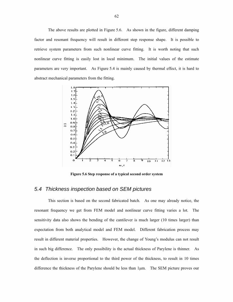
62
The above results are plotted in Figure 5.6. As shown in the figure, different damping
factor and resonant frequency will result in different step response shape. It is possible to
retrieve system parameters from such nonlinear curve fitting. It is worth noting that such
nonlinear curve fitting is easily lost in local minimum. The initial values of the estimate
parameters are very important. As Figure 5.4 is mainly caused by thermal effect, it is hard to
abstract mechanical parameters from the fitting.
Figure 5.6 Step response of a typical second order system
5.4 Thickness inspection based on SEM pictures
This section is based on the second fabricated batch. As one may already notice, the
resonant frequency we get from FEM model and nonlinear curve fitting varies a lot. The
sensitivity data also shows the bending of the cantilever is much larger (10 times larger) than
expectation from both analytical model and FEM model. Different fabrication process may
result in different material properties. However, the change of Young’s modulus can not result
in such big difference. The only possibility is the actual thickness of Parylene is thinner. As
the deflection is inverse proportional to the third power of the thickness, to result in 10 times
difference the thickness of the Parylene should be less than 1µm. The SEM picture proves our

63
conjection. From Figure 5.7d, the thickness of Parylene is actually less than 1µm. Possible
explanation is that Parylene layer is actually attacked during the DeepRIE process.
Figure 5.7 SEM pictures of tested second batch
devices. Cantilever is made of two layers: thin
aluminum layer and Parylene layer. Aluminum
layer peel off a little bit. Designed thickness of
Parylene layer and aluminum layer are 2µm and
30nm separately. The pictured device is on the
same die of the device we used for testing
e)
a) b)
c) d)

64
6 Conclusion
Testing results of fabricated devices show the transverse sensitivity of Lab-on-Tip device
is in pica Newton range, which is good enough for aforementioned single molecular DNA
sequencing purpose. Unlike force microscopy (AFM), our device is more sensitive to transverse
force. Thus Lab-on-Tip device actually provides a capability complementary to AFM, namely,
measurement of lateral forces with pico-Newton resolution. Since the “Lab” is on the “Tip”, this
non-blocking or open-space nature allows the combination of fluorescence microscopy and
various manipulation methods (laser tweezers, microneedles, nanotubes, fluid, etc.) with pN force
sensing capability. Therefore, the Lab-on-Tip device offers a new level of functionality and will
also be a useful tool for various studies such as nanotribology, biomechanics and so on.

65
Appendix A
//File Name mask.c 2005 05 28 //Description: Fill the closed polyline on certain layer. Source file //is in DXF format. A new file with name (source)_f.dxf is produced. //The polylines to be filled can be a part of internal blocks. //No need to explode it to fill such polylines. //Parameters: Source file name, grayscale, layer name //Further functions can be expected: the handling of line color, vertex, //shape, and size. //Author: Zhuo Wang, Wayne State University //Email: [email protected] #include <stdlib.h> #include <string.h> #include <stdio.h> #include <process.h> #define nChar 255 void fillpline(void); FILE *dxf,*ndxf; int npoly=0; // Number of closed polylines char value[nChar],Layer[nChar],chcode[nChar]; int grayscale; int code; int oddeven=0; void main() char fname[nChar],fname_new[nChar]; printf("\nEnter DXF file name:"); scanf("%s",fname); strcpy(fname_new,fname); strcat(fname_new,"_f"); strcat(fname,".dxf"); strcat(fname_new,".dxf"); printf("\ninput the Layer:"); scanf("%s",Layer); // strcat(Layer,"\n"); printf("input the grayscale:"); scanf("%d",&grayscale); if((dxf=fopen(fname,"r"))== NULL) printf( "The origin file was not opened\n" );exit(0); if((ndxf=fopen(fname_new,"w"))== NULL) printf( "The writing file was not opened\n" );exit(1);;

66
do do fgets(chcode, nChar, dxf); code=atoi(chcode); fgets(value,nChar,dxf); fputs(chcode,ndxf); fputs(value,ndxf); while((code != 0) || strcmp(value,"SECTION\n")); fgets(chcode, nChar, dxf); code=atoi(chcode); fgets(value,nChar,dxf); fputs(chcode,ndxf); fputs(value,ndxf); while((code != 2) || strcmp(value,"BLOCKS\n"));//ENTITIES\n while(!feof(dxf)) if(code == 0 && strcmp(value,"LWPOLYLINE\n") == 0) fillpline(); else fgets(chcode, nChar, dxf); code=atoi(chcode); fputs(chcode,ndxf); fgets(value,nChar,dxf); fputs(value,ndxf); fclose(dxf); fclose(ndxf); //----------- fill polyline() ------------ void fillpline(void) int banner; int ihelp; char buffer[nChar],*tmp1,*tmp2; banner=0; do fgets(chcode, nChar, dxf); code=atoi(chcode); fgets(value,nChar,dxf); tmp1=buffer; tmp2=value; ihelp=0; while (*tmp2!='\n')

67
if (ihelp==0&&*tmp2==' ') tmp2++; else *tmp1++=*tmp2++; ihelp=1; *tmp1='\0'; if (code==8&&strcmp(buffer,Layer)==0) banner=1; if (code!=0) fputs(chcode,ndxf); fputs(value,ndxf); while(code!=0); if (banner==1) fprintf(ndxf,"1001\nAUTOCAD_POSTSCRIPT_FIGURE\n"); fprintf(ndxf,"1002\n\n1000\nPSFILL\n"); fprintf(ndxf,"1000\nGrayscale\n1000\nGrayscale\n"); fprintf(ndxf,"%d\n%d\n",1070,grayscale); fprintf(ndxf,"1002\n\n"); npoly++; fputs(chcode,ndxf); fputs(value,ndxf);

68
Appendix B Material properties
Properties Parylene C
Young’s Molulus (psi) 400,000
Tensile Strength (psi) 10,000
Yield Strength 9,000
Elongation to Break (%) 200
Yield Elongation (%) 2.9
Density (g/cm3 ) 1.289
Refractive Index (nD23) 1.639
Thermal Conductivity, (10-4
cal./sec./cm2-°C/cm.)
~2
Linear Coefficient of Expansion,
(10-5/°C)
3.01
Specific Heat (cal/g- oC) 0.17
Melting Point (oC) 290
Glass Transition T (oC) 80-100

69
Appendix C Ansys command stream files
!This ANSYS command stream file perform general purpose FEM analysis !of a composite beam with varying covering ratio. !Auther: Zhuo Wang, Wayne State University, [email protected] !Last modified: 08/05/2006 /Title, Cantilever Beam ! All dims in um /PREP7 !DEFINE GEOMETRY WIDTH=100 LENGTH=500 THICKNESS=3 WIDTH_POLY=20 !WIDTH_POLY=width THICKNESS_POLY=0.5 LENGTH_POLY=LENGTH BLC4,0,0,WIDTH,THICKNESS,LENGTH BLC4,WIDTH/4-WIDTH_POLY/4,-THICKNESS_POLY,WIDTH_POLY/2,THICKNESS_POLY,LENGTH_POLY BLC4,3*WIDTH/4-WIDTH_POLY/4,-THICKNESS_POLY,WIDTH_POLY/2,THICKNESS_POLY,LENGTH_POLY !GLUE TWO LAYERS VGLUE,1,2,3 !DEFINE ELEMENTS ET,1,SOLID45 ! Change element type here !DEFINE MATERIALS MP,EX,1,0.003 !PARYLENE C MP,PRXY,1,0.4 MP,EX,2,0.168 !poly-Si MP,PRXY,2,0.22 ESIZE,5 ! Change the element size for Parylene here VSWEEP,4 TYPE, 1 MAT, 2 VSWEEP,2 VSWEEP,3 CPINTF,ALL,0.0001, !coicident node /SOLU ANTYPE,0 !APPLY LOAD !DEFINE DISPLANCEMENT CONSGTRAINTS ON AREAS ASEL,S,LOC,Z,0 DA,ALL,ALL,0

70
ASEL,ALL FK,14,FY,-0.0000001 !Define concentrated load SOLVE !Solve FINISH /POST1 !Enter post processor PLNSOL, U, SUM, 0,1 !Plot deflection

71
!This ANSYS command stream file perform harmonic analysis !of a composite beam with pole on tip. /SOLU ANTYPE,3 ! Harmonic analysis !APPLY LOAD !DEFINE DISPLANCEMENT CONSGTRAINTS ON AREAS ASEL,S,LOC,Z,0 DA,ALL,ALL,0 ASEL,ALL FK,24,FZ,1E-3 ! Apply force HARFRQ,430,435, ! Frequency range NSUBST,20, ! Number of frequency steps KBC,1 ! Stepped loads SOLVE FINISH /POST26 NSOL,2,1970,U,Y, UY_2 ! Get y-deflection data STORE,MERGE PRVAR,2 ! Print data PLVAR,2 ! Plot data !This ANSYS command stream file perform mode analysis !of a composite beam with a pole tip. !Auther: Zhuo Wang, Wayne State University, [email protected] !Last modified: 08/05/2006 /SOLU ANTYPE,2 ! Modal analysis MODOPT,SUBSP,5 ! Subspace, 5 modes EQSLV,FRONT ! Frontal solver MXPAND,5 ! Expand 5 modes !APPLY LOAD !DEFINE DISPLANCEMENT CONSGTRAINTS ON AREAS ASEL,S,LOC,Z,0 DA,ALL,ALL,0 ASEL,ALL SOLVE

72
!This ANSYS command stream file perform general purpose FEM analysis !of a composite beam with varying covering ratio. !Auther: Zhuo Wang, Wayne State University, [email protected] !Last modified: 08/05/2006 FINISH /CLEAR /Title, Cantilever Beam ! All dims in um /PREP7 !DEFINE GEOMETRY LENGTH=300 WIDTH=350 THICKNESS=2 THICKNESS_Al=0.03 OUTER_W=WIDTH !pole outer width INNER_W=WIDTH-50 !pole inner width LENGTH_POLE=500 !Length of the pole, most likely thickness of wafer WPROTA,0,90,0 BLC4,0,0,WIDTH,LENGTH+WIDTH+WIDTH WPROTA,0,-90,0 WPOFF,0,0,LENGTH BLC4,0,0,OUTER_W,LENGTH_POLE,OUTER_W WPOFF,0,0,25 BLC4,25,480,INNER_W,LENGTH_POLE,INNER_W VSBV,1,2 AOVLAP,1,4 !DEFINE ELEMENTS ET,1,SHELL99 ! 8 NODE LAYERED SHELL ELEMENT KEYOPT,1,8,1 R,1,2 ! 2 LAYERS PER ELEMENT RMORE RMORE,1,0,THICKNESS,2,0,THICKNESS_Al ! LAYER 1: Parylene; LAYER 2: Al MP,EX,1,0.003e6 !PARYLENE C MP,PRXY,1,0.4 MP,DENS,1,1289e-18 ! Density MP,EX,2,0.05e6 !Al MP,PRXY,2,0.33 MP,DENS,2,2700E-18 ESIZE,25 ! Change element size for Parylene here AMESH,4 AMESH,8 AMESH,5 ET,2,SOLID45 ! Change element type here

73
MP,EX,3,0.168e6 !Si MP,PRXY,3,0.17 MP,DENS,3,2330E-18 TYPE,2 MAT,3 MSHKEY,0 MSHAPE,1,3D ESIZE,50 !Change element size for pole here VMESH,3 /SOLU ANTYPE,static !APPLY LOAD !DEFINE DISPLANCEMENT CONSGTRAINTS ON A DL,1,,ALL,0 !acel,0,9.8e6,0 fk,16,fz,1e-6 SOLVE

74
Appendix D LabVIEW power spectrum details
The Power Spectrum Sxx(f) of a function x(t) is defined as Sxx(f) = X*(f)X(f) = |X(f)|2,
where X(f) = Fx(t), and X* (f) is the complex conjugate of X(f).
The Power Spectrum VI uses the FFT and DFT routines to compute the power spectrum,
which is given by Sxx(f)= | Fx(t)|2/n2, where Sxx represents the output sequence Power
Spectrum, and n is the number of samples in the input sequence X.
When the number of samples, n, in the input sequence X is a valid power of 2: n = 2m for
m = 1, 2, 3, …, 23, the Power Spectrum VI computes the Fast Fourier Transform of a real-valued
sequence using the a fast radix-2 FFT algorithm and efficiently scales the magnitude square. The
largest Power Spectrum the VI can compute using the FFT is 223 (8,388,608 or 8M).
When the number of samples in the input sequence X is not a valid power of 2 but is
factorable as the product of small prime numbers, the Power Spectrum VI computes the Discrete
Fourier Transform of a real-valued sequence using an efficient DFT algorithm and scales the
magnitude square. The largest Power Spectrum the VI can compute using the fast DFT is 222 -
1(4,194,303 or 4M - 1).
Let Y be the Fourier transform of the input sequence X and n be the number of samples in
it. You can show that |Yn - i|2 = |Y-i2|.
You can interpret the power in the (n - 1)th element of Y as the power in the -ith element
of the sequence, which represents the power in the -ith harmonic. You can find the total power for
the ith harmonic (DC and Nyquist component not included) using Power in the ith harmonic =
2|Yi|2 = |Yi|2 + |Yn - 1|2 0 < i < n/2. The total power in the DC and Nyquist components are
|Y0|2 and |Yn/2|2 respectively.
If n is even, let k=n/2. The following table shows the format of the output sequence Sxx
corresponding to the Power Spectrum.
Array Element Interpretation

75
Sxx0 Power in DC component Sxx1 = Sxx(n - 1) Power at frequency ∆f Sxx2 = Sxx(n - 2) Power at frequency 2∆f Sxx3 = Sxx(n - 3) Power at frequency 3∆f … … Sxx(k - 2) = Sxxn - (k - 2)
Power at frequency (k - 2) ∆ f
Sxx(k - 1) = Sxxn - (k - 1)
Power at frequency (k - 1) ∆ f
Sxxk Power in Nyquist harmonic The following illustration represents the preceding table information.
Notice that the power spectrum is symmetric about the Nyquist frequency as the
following illustration shows.
If n is odd, let k=(n-1)/2. The following table shows the format of the output sequence
Sxx corresponding to the Power Spectrum.
Array Element Interpretation

76
Sxx0 Power in DC component Sxx1 = Sxx(n - 1) Power at frequency ∆f Sxx2 = Sxx(n - 2) Power at frequency 2∆f Sxx3 = Sxx(n - 3) Power at frequency 3∆f … … Sxx(k - 2) = Sxxn - (k - 2)
Power at frequency (k - 2) ∆ f
Sxx(k - 1) = Sxxn - (k - 1)
Power at frequency (k - 1) ∆ f
Sxxk = Sxxn - k Power at frequency k∆f The following illustration shows that when n is odd, the power spectrum is symmetric
about the Nyquist frequency, but the Nyquist frequency does not fall on a frequency bin.
The format described in the preceding tables is an accepted standard in digital signal
processing applications.

77
Appendix E Matlab source codes
%The program calculate the strain and stress of a multilayer cantilever %All dimension related unit is in meter clear; x=[3e-6, 0.5e-6, 100e-6, 495e-6]; E=[3e9/(1-0.4^2),1.68e11/(1-0.22^2)]; % E is Young's modulus, unit: N/m^2; E(1) for Parylene, E(2) for Si %E=[3e9/(1-0.3^2),1.68e11/(1-0.3^2)] %E=[3e9,1.68e11]; Ep=E(2); % Young's modulus for piezoresistor t=[x(1:2)]; % t is thickness, unit: m; t(1) Parylene, t(2) Si c_w=0.2; w=[x(3), c_w*x(3)]; % w is width, unit: m l=x(4); % l is length, unit: m pi_l=-12.5e-11; %piezoresistive coefficients, unit m^2/N N=2; %how many turns we have <--- need to be changed n=1e20*1e6; % dopping concentration, unit: cm^-3->m^-3 rho_r=4e-3*1e-2; %resistivity for n=1e20, p type Si (Boron), from Sze p32; unit: Ohm*m; sigma=1e-4; %Surface stress, unit: N/m rho_m=[1289,2330]; % specific mass, unit: kg/m^3; f=[0.1,20]; Vin=1; %bias voltage, Unit: Volt <-------need to be changed %%%%%%%%%%%%%% The following are derived parameters %%%%%%%%%%%%% w_p=w(2); l_p=0.9*l; A=t.*w; % area of crosssection yci=[0,-(t(1)+t(2))/2]; % geometric center of each layer, in old coordinates y_p=yci(2); %geo center for piezo y_top=t(1)/2; y_c=sum(E.*A.*yci)/sum(E.*A); % coordinate of neutral plane Iz=w.*t.^3/12+(yci-y_c).^2.*A; % bending momentum around z axis m=rho_m.*A; fn=1/2/pi*1.875^2/l^2*sqrt(sum(E.*Iz)/sum(m)); t_p=t(2); Ap=A(2)/N; %area of piezoresistor, one strand R=N*rho_r*l_p/Ap; % resistance Sens_s=Vin/4*pi_l*Ep*w(1)*(y_p-y_c)*(y_top-y_c)/sum(E.*Iz); kB=1.38e-23; T=300; %Boltzmann constant, unit: J/K V_Johnson=4*kB*T*R*(f(2)-f(1));

78
alpha=0.0067; V_Hooge=alpha*(0.7*Vin)^2/(n*l_p*t_p*w_p)*log(f(2)/f(1)); Q=3; V_ThermalMech=Sens_s^2*8*pi*kB*T*l^3*sum(m)*fn/w(1)^2/(y_top-y_c)^2*(f(2)-f(1)); sigma_min=sqrt(V_Johnson+V_Hooge+V_ThermalMech)/Sens_s; strain_top=1e-7*l*(t(1)/2-y_c)/sum(E.*Iz) strain_bottom=1e-7*l*(-t(2)-t(1)/2-y_c)/sum(E.*Iz) %stress_top=E(1)*1e-6*l*(t(1)/2-y_c)/sum(E.*Iz) %stress_bottom=E(2)*1e-6*l*(-t(2)-t(1)/2-y_c)/sum(E.*Iz)

79
%The following program calculate the spot movement in two pictures. %Please put the .m file the same directory with the image files. %Change the image file name as necessary clear, close all %Processing of the first image Im1=imread('4.bmp'); %change file name here. Support bmp, jpg, png and etc. Im1=rgb2gray(Im1); %Change color image to grayscale image for easy handling subplot(2,2,1) imshow(Im1,[0,255]) %plot original image xlabel('Original Image #1') level=200; % change the threashold grayscale value here Im1=imsubtract(Im1,level); %substract background subplot(2,2,2) imshow(Im1,[0,255-level]) xlabel('Denoised Image #1') %Im=double(Im)+1; rou_y1=sum(Im1); % y is horizontal direction rou_x1=sum(Im1'); % x is vertical direction (characterizes rows) [x_d,y_d]=size(Im1); x=1:x_d; y=1:y_d; y_center1=y*rou_y1'/sum(rou_y1) x_center1=x*rou_x1'/sum(rou_x1) %Processing of the scond image Im2=imread('1.bmp'); %change file name here Im2=rgb2gray(Im2); subplot(2,2,3) imshow(Im2,[0,255]); xlabel('Original Image #2') Im2=imsubtract(Im2,level); %substract background subplot(2,2,4) imshow(Im2,[0,255-level]) xlabel('Denoised Image #2') rou_y2=sum(Im2); rou_x2=sum(Im2'); y_center2=y*rou_y2'/sum(rou_y2) x_center2=x*rou_x2'/sum(rou_x2) disp_y=y_center2-y_center1 %displacement in y direction disp_x=x_center2-x_center1 %displacement in x direction

80
%Main file of nonlinear curve fitting %Step response y=[1.732725 1.7296 ……. ]'; y=y-sum(y(1:557))/557; yy=y(557:2000); plot(yy) t=0:0.0005:0.0005*1443; !plot(t,yy) x0=[0.1,60,0.14]; [x,resnorm] = lsqcurvefit(@fun,x0,t,yy) yyy=fun(x,t); plot(t,yy,t,yyy) xlabel('time(second)') ylabel('PSD output(Volt)') %function file: fun.m %fitting of second order system %x(1) is kesi, x(2) is omega, x(3) is step amplitude function f=fun(x,t) del=(x(1)^2-1); f=x(3)+x(3)/(2*x(1)*del^0.5+2*del)*exp(-(x(1)*x(2)+del^0.5*x(2))*t)+x(3)/(-2*x(1)*del^0.5+2*del)*exp(-(x(1)*x(2)-del^0.5*x(2))*t);
81
References
1. F. Sanger, S. Nicklen, and A. R. Coulson, “DNA sequencing with chain-terminating
inhibitors”, Proc Natl Acad Sci, vol.74, pp.5463-5467, 1977
2. E. P. Kartalov and S. R. Quake, "Microfluidic device reads up to four consecutive base pairs
in DNA sequencing-by-synthesis," Nucleic Acids Research, vol. 32, pp. 2873-2879, 2004.
3. M. Ronaghi, M. Uhlen, and P. Nyren, "A sequencing method based on real-time
pyrophosphate," Science, vol. 281, pp. 363-+, 1998.
4. M. Ronaghi, S. Karamohamed, B. Pettersson, M. Uhlen, and P. Nyren, "Real-time DNA
sequencing using detection of pyrophosphate release," Analytical Biochemistry, vol. 242, pp.
84-89, 1996.
5. R. Drmanac, I. Labat, I. Brukner, and R. Crkvenjakov, "Sequencing of megabase plus DNA
by hybridization - theory of the method," Genomics, vol. 4, pp. 114-128, 1989.
6. S. Brenner, M. Johnson, J. Bridgham, G. Golda, D. H. Lloyd, D. Johnson, S. J. Luo, S.
McCurdy, M. Foy, M. Ewan, R. Roth, D. George, S. Eletr, G. Albrecht, E. Vermaas, S. R.
Williams, K. Moon, T. Burcham, M. Pallas, R. B. DuBridge, J. Kirchner, K. Fearon, J. Mao,
and K. Corcoran, "Gene expression analysis by massively parallel signature sequencing
(MPSS) on microbead arrays," Nature Biotechnology, vol. 18, pp. 630-634, 2000.
7. S. Brenner, S. R. Williams, E. H. Vermaas, T. Storck, K. Moon, C. McCollum, J. I. Mao, S. J.
Luo, J. J. Kirchner, S. Eletr, R. B. DuBridge, T. Burcham, and G. Albrecht, "In vitro cloning
of complex mixtures of DNA on microbeads: Physical separation of differentially expressed
cDNAs," Proceedings of the National Academy of Sciences of the United States of America,
vol. 97, pp. 1665-1670, 2000.
8. L. M. Smith, "Sequence from spectrometry: A realistic prospect?," Nature Biotechnology, vol.
14, pp. 1084-&, 1996.

82
9. E. B. Shera, N. K. Seitzinger, L. M. Davis, R. A. Keller, and S. A. Soper, "Detection of single
fluorescent molecules," Chemical Physics Letters, vol. 174, pp. 553-557, 1990.
10. J. D. Harding and R. A. Keller, "Single-molecule detection as an approach to rapid DNA
sequencing," Trends in Biotechnology, vol. 10, pp. 55-57, 1992.
11. H. Yu, J. Chao, D. Patek, R. Mujumdar, S. Mujumdar, and A. S. Waggoner, "Cyanine dye
dUTP analogs for enzymatic labeling of DNA probes," Nucleic Acids Research, vol. 22, pp.
3226-3232, 1994.
12. G. Binnig, C. F. Quate, and C. Gerber, "Atomic force microscope," Physical Review Letters,
vol. 56, pp. 930-933, 1986.
13. T. Boland and B. D. Ratner, "Direct measurement of hydrogen-bonding in DNA nucleotide
bases by atomic-force microscopy," Proceedings of the National Academy of Sciences of the
United States of America, vol. 92, pp. 5297-5301, 1995.
14. B. Essevaz-Roulet, U. Bockelmann, and F. Heslot, "Mechanical separation of the
complementary strands of DNA," Proceedings of the National Academy of Sciences of the
United States of America, vol. 94, pp. 11935-11940, 1997.
15. M. Rief, H. Clausen-Schaumann, and H. E. Gaub, "Sequence-dependent mechanics of single
DNA molecules," Nature Structural Biology, vol. 6, pp. 346-349, 1999.
16. J. L. Viovy, C. Heller, F. Caron, P. Cluzel, and D. Chatenay, "Ultrafast sequencing of DNA
by mechanical opening of the double helix - a theoretical investigation," Comptes Rendus De
L Academie Des Sciences Serie Iii-Sciences De La Vie-Life Sciences, vol. 317, pp. 795-800,
1994.
17. J. J. Kasianowicz, E. Brandin, D. Branton, and D. W. Deamer, "Characterization of
individual polynucleotide molecules using a membrane channel," Proceedings of the National
Academy of Sciences of the United States of America, vol. 93, pp. 13770-13773, 1996.
18. D. W. Deamer and M. Akeson, "Nanopores and nucleic acids: prospects for ultrarapid
sequencing," Trends in Biotechnology, vol. 18, pp. 147-151, 2000.

83
19. A. Meller, L. Nivon, E. Brandin, J. Golovchenko, and D. Branton, "Rapid nanopore
discrimination between single polynucleotide molecules," Proceedings of the National
Academy of Sciences of the United States of America, vol. 97, pp. 1079-1084, 2000.
20. A. Meller, L. Nivon, and D. Branton, "Voltage-driven DNA translocations through a
nanopore," Physical Review Letters, vol. 86, pp. 3435-3438, 2001.
21. D. W. Deamer and D. Branton, "Characterization of nucleic acids by nanopore analysis,"
Accounts of Chemical Research, vol. 35, pp. 817-825, 2002.
22. A. Meller and D. Branton, "Single molecule measurements of DNA transport through a
nanopore," Electrophoresis, vol. 23, pp. 2583-2591, 2002.
23. D. Branton and P. Leroy, "Nanopore analysis of nucleic acids," Biofutur, pp. A1-+, 2002.
24. H. Wang and D. Branton, "Nanopores with a spark for single-molecule detection," Nature
Biotechnology, vol. 19, pp. 622-623, 2001.
25. M. Akeson, D. Branton, J. J. Kasianowicz, E. Brandin, and D. W. Deamer, "Microsecond
time-scale discrimination among polycytidylic acid, polyadenylic acid, and polyuridylic acid
as homopolymers or as segments within single RNA molecules," Biophysical Journal, vol. 77,
pp. 3227-3233, 1999.
26. J. J. Nakane, M. Akeson, and A. Marziali, "Nanopore sensors for nucleic acid analysis,"
Journal of Physics-Condensed Matter, vol. 15, pp. R1365-R1393, 2003.
27. W. A. Vercoutere, S. Winters-Hilt, V. S. DeGuzman, D. Deamer, S. E. Ridino, J. T. Rodgers,
H. E. Olsen, A. Marziali, and M. Akeson, "Discrimination among individual Watson-Crick
base pairs at the termini of single DNA hairpin molecules," Nucl. Acids Res., vol. 31, pp.
1311-1318, 2003.
28. N. Ashkenasy, J. Sanchez-Quesada, H. Bayley, and M. Ghadiri, "Recognizing a single base
in an individual DNA strand: a step toward DNA sequencing in nanopores," Angewandte
Chemie International Edition, vol. 44, pp. 2-5, 2005.

84
29. A. J. Storm, D. van den Broek, S. Lemay, and C. Dekker, "Solid-state nanopores for
single-molecule DNA studies," Biophysical Journal, vol. 82, pp. 52a-52a, 2002.
30. A. J. Storm, J. H. Chen, X. S. Ling, H. W. Zandbergen, and C. Dekker, "Fabrication of
solid-state nanopores with single-nanometre precision," Nature Materials, vol. 2, pp. 537-540,
2003.
31. J. L. Li, D. Stein, C. Qun, E. Brandin, A. Huang, H. Wang, D. Branton, and J. Golovchenko,
"Solid state nanopore as a single DNA molecule detector," Biophysical Journal, vol. 84, pp.
134a-135a, 2003.
32. A. Marziali and M. Akeson, "New DNA sequencing methods", Annual Review of
Biomedical Engineering, vol. 3, pp. 195-223, 2001.
33. R. J. Roark, W. C. Young, “Formulas for Stress and Strain”, McGraw-Hill Book Co., Inc.,
New York, NY, 1975
34. C.A. Klein, “How accurate are Stoney’s equation and recent modifications”, Journal of
Applied Physics, vol.88, pp.5487-5489, 2000
35. L.B. Freund, J.A. Floro, E. Chason, “Extensions of the Stoney formula for substrate curvature
to configurations with thin substrates or large deformations”, Applied Physics Letters, vol.74,
pp.1987-1989, 1999
36. M.S. Weinberg, “Working equations for piezoelectric actuators and sensors”, Journal of
Microelectromechanical Systems, vol.8, pp529-533, 1999
37. P.P. Benham, R.J. Crawford, and C.G. Armstrong “Mechanics of Engineering Materials 2nd
ed”, 1996.
38. S. Timoshenko and W.W. Krieger, “Theory of plates and shells”, McGraw-Hill, 1959
39. Ansys8.1 help system, “Modeling and meshing guide”, 2003
40. Y.Sugiyama et.al. High sensitive magnetic sensor made of AlGaAs/GaAs heterojunction
semiconductor. Proceeding of the 6th sensors symposium, pp. 55-60, 1986
41. S.M. Sze, “Physics of semiconductor devices”, John Wiley and Sons, 1981

85
42. J.D. Jackson, “Classical electrodynamics (3rd ed)”, New York Wiley, 1999
43. J. Schwinger, “Classical electrodynamics”, Perseus Books, 1998
44. P. Lorrain, D.R. Corson, “Electromagnetic fields and waves : including electric circuits 3rd
ed”, New York : Freeman, 1988
45. K.Q. Zhang, D.J. Li, “Electromagnetic Theory for Microwaves and Optoelectronics”,
Springer-Verlag, 1999
46. M. Born, E. Wolf, “Principles of optics: Electromagnetic Theory of Propagation, Interference
and Diffraction of Light”, Cambridge University Press, 1999
47. H. Kogelnik and T. Li, “Laser beams and Resonators”, Applied Optics, Vol. 5, pp. 1550-1567,
1966
48. A. Yariv, “Optical Electronics in Modern Communication”, Oxford, 1997
49. R.E. Fischer, B.T. Galeb, “Optical system design”, McGraw-Hill, 2000
50. OSLO Optical Reference (release 6.1)
51. B. Ilic, S. Krylov, K. Aubin, R. Reichenbach, and H. G. Craighead, “Optical excitation of
nanoelectromechanical oscillators”, Applied Physics Letters, Vol.86, pp. 193114-193116
(2005)
52. G.S. Hu, “Digital Signal Processing, theory, algorism and implementation”, Tsinghua
University Press, 2003 (in Chinese)
53. K.R. Castleman, “Digital Image Processing”, Prentice Hall, 1996

86
Abstract
A NOVEL LAB-ON-TIP NANOMECHANICAL PLATFORM FOR SINGLE MOLECULE DNA SEQUENCING
by
ZHUO WANG
August 2006
Advisor: Dr. Yong Xu
Major: Electrical Engineering
Degree: Master of Science
As we are entering the post-genomic era, low cost and fast DNA sequencing is highly
desired. The thesis reports the successful prototype development of a novel Lab-on-Tip device that
provides a lateral force measurement with pN (pico-Newton) resolution. Corresponding finite
element model of the device and analytical model for composite beam are developed to supply design
guideline. A complete ray-tracing model and a testing platform based on virtual instrument are also
developed to ease the testing configuration. This Lab-on-Tip device is constructed by fabricating a
vertical pole on a lateral cantilever beam. Micro/nanofluidic components can be incorporated on the
tip to perform various biological analyses, e.g. single molecular DNA sequencing through a nanopore.
The lateral force on the tip can be amplified and translated to the bottom cantilever beam via the
vertical pole. The deflection of the bottom cantilever is then detected by optical lever method or
piezoresistor, just like AFM, with a pN resolution. Since the “Lab” is on the “Tip”, this non-blocking
or open-space nature allows the combination of fluorescence microscopy and various manipulation
methods (laser tweezers, microneedles, nanotubes, fluid, etc.) with pN force sensing capability.
Besides the single molecular DNA sequencing, the Lab-on-Tip device also offers a new level of
functionality and will be a useful tool for various studies such as nanotribology, biomechanics and so
on.

87
Autobiographical Statement
My interest in science dates back to my personal experience. In the
elementary school, for the first time, I made a radio by myself. I still remember
the joy of hearing the music flow out of the speaker, though I did not know the
theory behind the radio at that time. In senior high school, I made a telescope
to observe comets. My buddies and I rode to environs in a cold spring night for
the attractive Hale-Bopp Comet.
I chose Tsinghua University for my four years of undergraduate study. It
is the best university in China. I got well-rounded training in my major and
gained better and deeper understanding of it. After that, I worked as an
engineer in Tsinghua-Foxconn Nanotechnology Research Center for two years.
Later I entered Wayne State University, Detroit, MI to pursue my master
degree. Wayne State has a fairly good MEMS foundry, where I learned a lot of
fabrication and testing techniques. Sadly, the most important person in my
life-my father happened passed away in Feb.,2006. I am still in great sorrow
and can not believe this truth. I would rather believe there is another world
called heaven now and hope he can have a peaceful life there.