a novel high conversion ratio bi-directional dc-dc converter · thebi-directional converter can...
TRANSCRIPT

International Journal of Science and Research (IJSR) ISSN (Online): 2319-7064
Index Copernicus Value (2013): 6.14 | Impact Factor (2015): 6.391
Volume 5 Issue 9, September 2016 www.ijsr.net
Licensed Under Creative Commons Attribution CC BY
A Novel High Conversion Ratio Bi-Directional DC-DC ConverterSarun S S1, Anil J Thomas2
1PG Student [PEPS], Department of EEE, FISAT, Angamaly, Kerala, India
2Assistant professor, Department of EEE, FISAT, Angamaly, Kerala, India
Abstract: This paper presents a high-conversion ratio bi-directional dc-dc converter with coupled inductor. In the boost mode, twocapacitors are parallel charged and series discharged by the coupled inductor. Thus, high step-up voltage gain can be achieved with anappropriate duty ratio. The voltage stress on the main switches reduced by a passive clamp circuit. Therefore, the low resistanceRDS(ON) of the main switch can be adopted to reduce conduction loss. In the buck mode, two capacitors are series charged and paralleldischarged by the coupled inductor. The bi-directional converter can have high step-down gain. Aside from that, all of the switchesachieve zero voltage-switching turn-on, and the switching loss can be reduced. Due to two active clamp circuits, the energy of theleakage inductor of the coupled inductor is recycled. The efficiency can be further improved. Simulation of open loop and closed loopcontrol of novel high-conversion-ratio bi-directional dc-dc converter with coupled inductor is done in MATLAB and output is obtained.Hardware implementation of the open loop is being done and the output is obtained.
Keywords: DC-DC Converter, Boost Mode, BuckMode ,Zero Voltage Switching, MATLAB/SIMULINK
1. Introduction
Renewable energy sources such as wind and solar are widely used nowadays. The output voltage of these sources is very low. Also sudden load changes cannot met by these sources. Therefore battery with bi-directional DC-DC converter isneeded [1] - [3]. Isolated bidirectional dc-dc converters such as half and full bridge types, can provide high step-up and step-down voltage gains by adjusting the turns ratio of the transformer. The high step-up gain and the high step-down voltage gain can be achieved. The leakage inductor of the transformer leads to the HV spike on the main switch during switching transition. A novel soft commutating isolated boost full-bridge zero-voltage-switching (ZVS) pulse width modulation dc-dc converter is introduced [4]. The energy ofthe leakage inductor is recycled and not dissipated. However, the number of switches is increased. To achieve a high conversion ratio, two inductors charged in parallel and discharged in series are proposed [5].Based on above topologies, the novel bidirectional converter combines all advantages such as high conversion ratio, recycling of the inductor energy, soft switching and high efficiency etc.in this converter a mutually coupled inductor and twocapacitors are used to achieve the high conversion ratio. The inductor energy is also recycled by using another capacitor. Soft switching is also obtainedin the converter. So thatswitching losses are minimized. Therefore converter has gothigh efficiency.
2. Operating Principle of the Novel High Conversion Ratio Bi-Directional DC-DC Converter
The switched-capacitor technique in [5] and [6] has proposed that parallel-chargedand series-discharged capacitors can achieve high step-up gain. Also, series charged and parallel-discharged capacitors can achieve high step-down gain.Thecharacter of the coupled inductor is that the secondary side can have oppositepolarity when the
switch is on and off. In the boost-state operation, this character is combined with the switched capacitor technique. Two capacitors C2 andC3 are parallel charged when the switch is on and series discharged when theswitch is off. Inthe buck-state operation, the coupled inductor is used asatransformer. Thus, two capacitors C2 and C3 can be series charged by HV sideand parallel discharged through thesecondary side. In addition, the problem ofthe energy of the leakage inductor is also solved. In the boost-state operation,S1 is the main switch, and capacitor C1 recycles the energy. The voltage acrossswitch S1 can be clamped. Since switch S1 has an LV level, the low conductingresistance RDS(ON) of the switch is used toreduce the conduction loss. In thebuck-state operation, themain switches are S2 and S5. Two capacitors C2 andC3 with switches S3 and S4 are used as active clamp circuits, recycling the energyof the leakage inductor on the secondary side of the coupled inductor. CapacitorC1 with switch S2 isanother active clamp circuit that recycled the energy ofthe leakage inductor on the primary side.
Figure 1: Circuit configuration of the bidirectionalconverter
Thus, four switches are ZVS turned on. The switching loss isimproved; the efficiency can be increased. It is because that the high step-up converter needs a large input current, which results that the conduction loss is larger than the switching loss. Thus, reducing the switch voltage stress for alleviating the conduction loss and the elimination of reverse-recovery
Paper ID: ART20161833 1438
International Journal of Science and Research (IJSR) ISSN (Online): 2319-7064
Index Copernicus Value (2013): 6.14 | Impact Factor (2015): 6.391
Volume 5 Issue 9, September 2016 www.ijsr.net
Licensed Under Creative Commons Attribution CC BY
current is the key point to improve efficiency. Similarly, the main switch of the high step-up and step-down converters suffers HV stress and low conducting current. The switching loss should be reduced to improve efficiency.
A. Boost Mode Operation
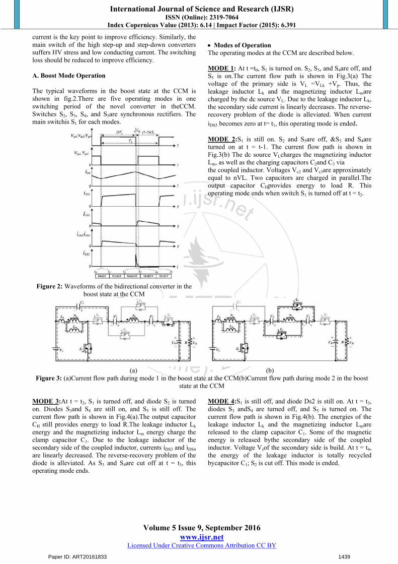
The typical waveforms in the boost state at the CCM isshown in fig.2.There are five operating modes in oneswitching period of the novel converter in theCCM.Switches S2, S3, S4, and S5are synchronous rectifiers. Themain switchis S1 for each modes.
Figure 2: Waveforms of the bidirectional converter in theboost state at the CCM
Modes of OperationThe operating modes at the CCM are described below.
MODE 1: At t =t0, S1 is turned on. S2, S3, and S4are off, and S5 is on.The current flow path is shown in Fig.3(a) The voltage of the primary side is VL =VLk +Vp. Thus, theleakage inductor Lk and the magnetizing inductor Lmare charged by the dc source VL. Due to the leakage inductor Lk, the secondary side current is linearly decreases. The reverse-recovery problem of the diode is alleviated. When current iDS5 becomes zero at t= t1, this operating mode is ended.
MODE 2:S1 is still on. S2 and S5are off, &S3 and S4are turned on at t = t-1. The current flow path is shown inFig.3(b) The dc source VLcharges the magnetizing inductor Lm, as well as the charging capacitors C2and C3 via the coupled inductor. Voltages Vc2 and Vc3are approximately equal to nVL. Two capacitors are charged in parallel.The output capacitor CHprovides energy to load R. This operating mode ends when switch S1 is turned off at t = t2.
(a) (b) Figure 3: (a)Current flow path during mode 1 in the boost state at the CCM(b)Current flow path during mode 2 in the boost
state at the CCM
MODE 3:At t = t2, S1 is turned off, and diode S2 is turnedon. Diodes S3and S4 are still on, and S5 is still off. Thecurrent flow path is shown in Fig.4(a).The output capacitorCH still provides energy to load R.The leakage inductor Lkenergy and the magnetizing inductor Lm energy charge theclamp capacitor C1. Due to the leakage inductor of thesecondary side of the coupled inductor, currents iDS3 and iDS4are linearly decreased. The reverse-recovery problem of thediode is alleviated. As S3 and S4are cut off at t = t3, thisoperating mode ends.
MODE 4:S1 is still off, and diode Ds2 is still on. At t = t3, diodes S3 andS4 are turned off, and S5 is turned on. The current flow path is shown in Fig.4(b). The energies of the leakage inductor Lk and the magnetizing inductor Lmare released to the clamp capacitor C1. Some of the magnetic energy is released bythe secondary side of the coupled inductor. Voltage Vsof the secondary side is build. At t = t4, the energy of the leakage inductor is totally recycled bycapacitor C1; S2 is cut off. This mode is ended.
Paper ID: ART20161833 1439

International Journal of Science and Research (IJSR) ISSN (Online): 2319-7064
Index Copernicus Value (2013): 6.14 | Impact Factor (2015): 6.391
Volume 5 Issue 9, September 2016 www.ijsr.net
Licensed Under Creative Commons Attribution CC BY
(a) (b) Figure 4: (a)Current flow path during mode 3 in the boost state at the CCM (b) Current flow path during mode 4 in the boost
state at the CCM
MODE 5:S1 is still off and S2 is on, diodes S3 and S4are stilloff, and S5is still on. The current flow path is shown in Fig.The coupled inductor, dc source VL, and capacitors C2 andC3 are connected in series to charge the output capacitor CHand load R. The HV gain is achieved. This operating modeendsat t = t5 when switch S2 is turned off and S1 is turned onat the beginning of the next switching period.
Figure 5: Current flow path during mode 5 in the boost stateat the CCM
B. Buck Mode OperationIn buck mode, there are six operating modes in oneswitching period. The main switch is S5. Switches S2,S3 andS4 are auxiliary switches for achieving ZVS turn-on. Thetypical waveforms in the boost state at the CCM is shown inFig.6.
Figure 6: Waveforms of the bidirectional converter in thebuck state at the CCM
Modes of Operation
MODE 1:The switch S2 is turned on at t = t0. The current flow path is shownin Fig.7(a). Due to the leakage inductor Lk, the current of the secondary side of the coupled inductor flows through diode Ds5. Capacitors C1, C2, and C3are also discharged to VH. Then, switch S5 is turned on, and ZVS isachieved. Because of the HV side VH, current iDS1 and iDS5linearly decrease. Meanwhile, the output capacitor CL ischarged by the magnetizing energy. At t=t1, this mode isended. iDS5 become zero.
MODE 2:The switch S5 is turned on. The output capacitor CL provides energy to load R. Capacitors C1, C2, and C3, and the secondary side coil Ns are charged in series by HV side VH. Thus, the induced voltage Vp on the primary-side coil Np makes current iDS1 decrease and charge the magnetizing inductor Lm. The magnetizing current iLm is increased. At t = t2,this mode is ended. the current iDS1 become equal to zero.
Paper ID: ART20161833 1440

International Journal of Science and Research (IJSR) ISSN (Online): 2319-7064
Index Copernicus Value (2013): 6.14 | Impact Factor (2015): 6.391
Volume 5 Issue 9, September 2016 www.ijsr.net
Licensed Under Creative Commons Attribution CC BY
Figure 7: (a) Currentflow path during mode 1 in the buck state at the CCM(b)Current flow path during mode 2 in the buckstate at the CCM
MODE 3: The switch S5 is on. The leakage inductor Lk ischarged by the primary-side coil Np. The charge currentflows through the antiparallel diode Ds2 of switch S2. Then,S2 is turned on, and ZVS is achieved. Capacitors C1, C2, andC3 , and the secondary side coil Ns are still charged in seriesby HV side VH, and the magnetizing inductor Lm is alsocharged. The output capacitor CL provides the energy to loadR.At t = t3, iDS2 is equal to zero. This mode is ended.
MODE 4: The switches S2 and S5 are on. At t = t3, capacitor C1 starts to charge the magnetizing inductor Lm. The output capacitor CL discharges to load R. Because two capacitors C2 and C3, and the coupled inductor are charged in series bythe HV side VH, the high step-down voltage gain can beachieved. At t = t4, switches S2 and S5are turned off. This mode is ended.
Figure 8: (a) Current flow path during mode 3 in the buck state at the CCM (b)Current flow path during mode 4 in the buckstate at the CCM
MODE 5:The switches S2 and S5 are turned off at t=t4. The current ofthe leakage inductor flows through the antiparallel diodes Ds1, Ds3, and Ds4of switches. Then, switches S3 and S4are turned on, and ZVS turn on is achieved. The energy ofthe magnetizing inductor Lm discharges to capacitor CL and loadR. At t = t5, currents iDS3 and iDS4 are zero. This mode isended.
MODE 6:The switches S3 and S4 are on. At t = t5, the energy of capacitorsC2 and C3 discharges to the output capacitor CLand load R through the coupled inductor. The magnetizing inductor Lm also discharges to the output. This mode is ended at t = t6 when S3 and S4 are off.
Figure 9: (a) Currentflow path during mode 5 in the buckstate at the CCM (b)Current flow path during mode 6 in the
buck state at the CCM
3. Steady State Analysis of the Novel Converter
According to the assumptions before the steady stateanalysis, the equations of the turn ratio and the couplingcoeffcients k of the coupled inductor are defined as,
𝑛 =𝑁𝑠
𝑁𝑝
𝑘 =𝐿𝑚
𝐿𝑚 + 𝐿𝑘
The voltage gain of the boost-state operation is obtained as,
𝑀𝑏𝑜𝑜𝑠𝑡 =𝑉𝐻
𝑉𝐿
=1 + 𝑛
1 − 𝐷+ 𝑛
The voltage gain of the buck-state operation is obtained as,
𝑀𝑏𝑢𝑐𝑘 =𝑉𝐿
𝑉𝐻=
𝐷
1 + 𝑛 + 𝐷𝑛
The value of the magnetic inductor can be decided by,
𝐿𝑚 =𝐷(1 − 𝐷)2 𝑅𝐻
2(1 + 𝑛)(1 + 2𝑛 − 𝑛𝐷)𝑓𝑠where RH is the load, D is the duty ratio and fs is theswitching frequency. HereLm is 60µH and Lk is 0.16 µH.Thecapacitor C1 is 47 µF and C2 and C3 are of23.5 µF. Thevalue of capacitors C2 and C3 are obtained as,
𝐶2 = 𝐶3 >( 1 − 𝐷 𝑇2
𝜋2𝑛2𝐿𝑘
Paper ID: ART20161833 1441

International Journal of Science and Research (IJSR) ISSN (Online): 2319-7064
Index Copernicus Value (2013): 6.14 | Impact Factor (2015): 6.391
Volume 5 Issue 9, September 2016 www.ijsr.net
Licensed Under Creative Commons Attribution CC BY
4. Simulink Model and Results
A. Open Loop Control of Boost Mode Operation
The simulation diagram of bi-directional dc-dc boost converter is shown below.
Figure 10: Simulation diagram of bi-directional dc-dc boost converter in MATLAB
The input voltage and output voltage waveforms obtained inMATLAB Simulink are shown in the Fig.11 and Fig .12.
Figure 11: Input voltage (6V) waveform of bi-directional dc-dc boost converter
Figure 12: Output voltage (52V) waveform of bi-directional dc-dc boost converter
The input voltage is 6V. The output voltage obtained aftersimulation is 52V.
B. Open Loop Control of Buck Mode Operation The simulation diagram of bi-directional dc-dc buck converter is shown below.
Paper ID: ART20161833 1442

International Journal of Science and Research (IJSR) ISSN (Online): 2319-7064
Index Copernicus Value (2013): 6.14 | Impact Factor (2015): 6.391
Volume 5 Issue 9, September 2016 www.ijsr.net
Licensed Under Creative Commons Attribution CC BY
Figure 13: Simulation diagram of bi-directional dc-dc buck converter in MATLAB
The input voltage and output voltage waveforms obtained inMATLAB Simulink are shown in the Fig.14 and Fig .15
Figure 14: Input Voltage (24V) waveform of bi-directional dc-dc buck converter
Figure 15: Input Voltage (3V) waveform of bi-directional dc-dc buck converter
The input voltage is 24 V. The output voltage obtained aftersimulation is 3V.
C. Closed Loop Control of Boost Mode Operation
The simulation of the closed loop bi-directional converter isdone and the resultis obtained. The reference output voltage is set to 35 V. The initial input voltage is set as 5 V and finalinput voltage is set as 10 V. Closed loop is obtained usingpi controller. The simulation results are shown below.
Paper ID: ART20161833 1443

International Journal of Science and Research (IJSR) ISSN (Online): 2319-7064
Index Copernicus Value (2013): 6.14 | Impact Factor (2015): 6.391
Volume 5 Issue 9, September 2016 www.ijsr.net
Licensed Under Creative Commons Attribution CC BY
Figure 16: Closed loop simulation diagram of bi-directional dc-dc boost converter
Figure 17: Closed loop input and output voltage of bi-directional dc-dc boost converter
5. Hardware Implementation
The simulation is done by using MATLAB software and practical prototypeis made in the experimental environment. Hardware implementation of the bi-directional dc-dc boost converter with coupled inductor is done. Figure below shows the experimental set up. The switching pulses are generated using Arduino .And TLP250 is used asoptocoupler and IRF350 is used as the switch. For an inputvoltage of 6V, an output voltage of 24 V is obtained here.
Figure 18: Hardware Setup
Figure 19: Gating Signal generated from Arduino
Input and output voltage waveform is shown below.
Paper ID: ART20161833 1444

International Journal of Science and Research (IJSR) ISSN (Online): 2319-7064
Index Copernicus Value (2013): 6.14 | Impact Factor (2015): 6.391
Volume 5 Issue 9, September 2016 www.ijsr.net
Licensed Under Creative Commons Attribution CC BY
Figure 20: Input and output voltage waveform
6. Conclusion
A novel, high efficiency, and high step-up/step-down bidirectional dc-dc converter has been introduced here. Byusing the capacitor charged in parallel and discharged inseries by the coupled inductor, proposed converter have been discussed. The voltage gain and the utility rate of the magnetic core have been increased by using a coupled inductor with a low turn ratio. The energy of the leakage inductor has been recycled with the clamp circuit. The simulation of the converter for open loop and closed loop isdone in MATLAB and results are obtained. And also the hardware implementation of the bi-directional boost converter is done and boost output is regulated using the picontroller.
References
[1] Yi-Ping Hsieh, Jiann-Fuh Chen, Lung-Sheng Yang, Chang-Ying Wu, andWei-Shih Liu, “High ConversionRatio Bidirectional DC-DC Converter WithCoupledInductor",IEEE Trans. in Power Electronics, vol. 61,NO.1, Jan.2014.
[2] Roger Gules, Juliano De Pellegrin Pacheco, Hlio LeesHey and JohninsonImho,“A Maximum Power PointTracking System With Parallel Connectionfor PV Stand-Alone Applications",IEEE Trans. Ind. Electron.,vol. 55,NO.7, July. 2008.
[3] Rong-Wai and Rou-Yong Duan,“High-EfficiencyBidirectional Converter forPower Sources With GreatVoltage Diversity",,IEEE Trans. Ind. Electron.,vol. 22,NO. 5, Sept. 2007.
[4] [4] T. F. Wu, Y. C. Chen, J. G. Yang, and C. L. kuo,“Isolated bidirectional full bridge dc-dc converter with aybacksnubber", IEEE Trans. Power Electron.,vol. 25, no.7, pp. 1915-1922, Jul. 2010.
[5] L. S. Yang and T. J. Liang, “Analysis andimplementation of a novel bidirectional dc-dc converter",IEEE Trans. Ind. Electron., vol. 59, no. 1, pp.422-434,Jan. 2012.
[6] Fanghua Zhang and Yangguang Yan, “Novel ForwardFlyback Hybrid Bidirectional DC-DC Converter,"IEEETrans. Ind. Electron.,vol.56, NO. 5, May2009.
[7] Mohammad Reza Mohammadi and HoseinFarzanehfard,“New Family of Zero-Voltage-Transition PWM Bidirectional Converters With Coupled
Inductors,”IEEE Trans. Ind. Electron.,vol.59, NO. 2,Feb. 2012.
[8] Pritam Das, S. Ahmad Mousavi, and GerryMoschopoulos, “Analysis and Design of a NonisolatedBidirectional ZVS-PWM DC-DC Converter WithCoupled Inductors,"IEEE Trans. in PowerElectronics,vol.25,NO.10,Oct.2010..
Paper ID: ART20161833 1445